US7130216B2 - One-device non-volatile random access memory cell - Google Patents
One-device non-volatile random access memory cellDownload PDFInfo
- Publication number
- US7130216B2 US7130216B2US10/788,230US78823004AUS7130216B2US 7130216 B2US7130216 B2US 7130216B2US 78823004 AUS78823004 AUS 78823004AUS 7130216 B2US7130216 B2US 7130216B2
- Authority
- US
- United States
- Prior art keywords
- diode
- floating plate
- diffusion region
- region
- forming
- Prior art date
- Legal status (The legal status is an assumption and is not a legal conclusion. Google has not performed a legal analysis and makes no representation as to the accuracy of the status listed.)
- Expired - Lifetime, expires
Links
- 238000007667floatingMethods0.000claimsabstractdescription104
- 238000009792diffusion processMethods0.000claimsabstractdescription102
- 239000012212insulatorSubstances0.000claimsabstractdescription62
- 210000000746body regionAnatomy0.000claimsabstractdescription54
- 239000000758substrateSubstances0.000claimsdescription58
- 229910021332silicideInorganic materials0.000claimsdescription52
- 229910052751metalInorganic materials0.000claimsdescription37
- 239000002184metalSubstances0.000claimsdescription37
- 238000000034methodMethods0.000claimsdescription36
- FVBUAEGBCNSCDD-UHFFFAOYSA-Nsilicide(4-)Chemical compound[Si-4]FVBUAEGBCNSCDD-UHFFFAOYSA-N0.000claimsdescription36
- 239000004065semiconductorSubstances0.000claimsdescription21
- 238000003860storageMethods0.000claimsdescription21
- 230000002441reversible effectEffects0.000claimsdescription19
- 150000004706metal oxidesChemical class0.000claimsdescription16
- 229910044991metal oxideInorganic materials0.000claimsdescription14
- 229910000314transition metal oxideInorganic materials0.000claimsdescription13
- 229910021350transition metal silicideInorganic materials0.000claimsdescription10
- 238000007599dischargingMethods0.000claimsdescription6
- 230000006870functionEffects0.000claimsdescription5
- 230000015556catabolic processEffects0.000claimsdescription4
- 238000004519manufacturing processMethods0.000claimsdescription4
- 230000005641tunnelingEffects0.000claimsdescription4
- 239000000969carrierSubstances0.000claimsdescription2
- 238000005513bias potentialMethods0.000claims2
- VYPSYNLAJGMNEJ-UHFFFAOYSA-NSilicium dioxideChemical compoundO=[Si]=OVYPSYNLAJGMNEJ-UHFFFAOYSA-N0.000description26
- 230000004888barrier functionEffects0.000description16
- 239000000377silicon dioxideSubstances0.000description13
- 229910021420polycrystalline siliconInorganic materials0.000description9
- 229920005591polysiliconPolymers0.000description8
- 238000010586diagramMethods0.000description7
- 230000008569processEffects0.000description7
- 238000000231atomic layer depositionMethods0.000description6
- 230000014759maintenance of locationEffects0.000description6
- 229910052710siliconInorganic materials0.000description6
- 239000010703siliconSubstances0.000description6
- 230000008859changeEffects0.000description5
- XUIMIQQOPSSXEZ-UHFFFAOYSA-NSiliconChemical compound[Si]XUIMIQQOPSSXEZ-UHFFFAOYSA-N0.000description4
- 230000015572biosynthetic processEffects0.000description4
- 239000003990capacitorSubstances0.000description4
- 238000002955isolationMethods0.000description4
- MCMNRKCIXSYSNV-UHFFFAOYSA-NZrO2Inorganic materialsO=[Zr]=OMCMNRKCIXSYSNV-UHFFFAOYSA-N0.000description3
- PNEYBMLMFCGWSK-UHFFFAOYSA-Naluminium oxideInorganic materials[O-2].[O-2].[O-2].[Al+3].[Al+3]PNEYBMLMFCGWSK-UHFFFAOYSA-N0.000description3
- 229910052593corundumInorganic materials0.000description3
- 239000000463materialSubstances0.000description3
- 229910001845yogo sapphireInorganic materials0.000description3
- 229910021354zirconium(IV) silicideInorganic materials0.000description3
- 229910052581Si3N4Inorganic materials0.000description2
- 238000004891communicationMethods0.000description2
- 238000013461designMethods0.000description2
- 238000005516engineering processMethods0.000description2
- 239000007943implantSubstances0.000description2
- 239000012535impuritySubstances0.000description2
- 239000011159matrix materialSubstances0.000description2
- 239000002105nanoparticleSubstances0.000description2
- 239000002245particleSubstances0.000description2
- 238000012545processingMethods0.000description2
- 235000012239silicon dioxideNutrition0.000description2
- HQVNEWCFYHHQES-UHFFFAOYSA-Nsilicon nitrideChemical compoundN12[Si]34N5[Si]62N3[Si]51N64HQVNEWCFYHHQES-UHFFFAOYSA-N0.000description2
- 238000012546transferMethods0.000description2
- 229910018999CoSi2Inorganic materials0.000description1
- 229910005883NiSiInorganic materials0.000description1
- 230000006978adaptationEffects0.000description1
- 238000003491arrayMethods0.000description1
- 229910017052cobaltInorganic materials0.000description1
- 239000010941cobaltSubstances0.000description1
- GUTLYIVDDKVIGB-UHFFFAOYSA-Ncobalt atomChemical compound[Co]GUTLYIVDDKVIGB-UHFFFAOYSA-N0.000description1
- 230000001351cycling effectEffects0.000description1
- 238000006731degradation reactionMethods0.000description1
- 230000001419dependent effectEffects0.000description1
- PCHJSUWPFVWCPO-UHFFFAOYSA-NgoldChemical compound[Au]PCHJSUWPFVWCPO-UHFFFAOYSA-N0.000description1
- 239000010931goldSubstances0.000description1
- 229910052737goldInorganic materials0.000description1
- CJNBYAVZURUTKZ-UHFFFAOYSA-Nhafnium(IV) oxideInorganic materialsO=[Hf]=OCJNBYAVZURUTKZ-UHFFFAOYSA-N0.000description1
- 230000003993interactionEffects0.000description1
- 230000007246mechanismEffects0.000description1
- 150000002739metalsChemical class0.000description1
- 229910021334nickel silicideInorganic materials0.000description1
- RUFLMLWJRZAWLJ-UHFFFAOYSA-Nnickel silicideChemical compound[Ni]=[Si]=[Ni]RUFLMLWJRZAWLJ-UHFFFAOYSA-N0.000description1
- QGLKJKCYBOYXKC-UHFFFAOYSA-NnonaoxidotritungstenChemical compoundO=[W]1(=O)O[W](=O)(=O)O[W](=O)(=O)O1QGLKJKCYBOYXKC-UHFFFAOYSA-N0.000description1
- 230000002093peripheral effectEffects0.000description1
- 238000004886process controlMethods0.000description1
- 230000000717retained effectEffects0.000description1
- 125000006850spacer groupChemical group0.000description1
- GWEVSGVZZGPLCZ-UHFFFAOYSA-Ntitanium dioxideInorganic materialsO=[Ti]=OGWEVSGVZZGPLCZ-UHFFFAOYSA-N0.000description1
- 150000003624transition metalsChemical class0.000description1
- WFKWXMTUELFFGS-UHFFFAOYSA-NtungstenChemical compound[W]WFKWXMTUELFFGS-UHFFFAOYSA-N0.000description1
- 229910052721tungstenInorganic materials0.000description1
- 239000010937tungstenSubstances0.000description1
- 229910001930tungsten oxideInorganic materials0.000description1
Images


Classifications
- H—ELECTRICITY
- H10—SEMICONDUCTOR DEVICES; ELECTRIC SOLID-STATE DEVICES NOT OTHERWISE PROVIDED FOR
- H10D—INORGANIC ELECTRIC SEMICONDUCTOR DEVICES
- H10D8/00—Diodes
- H10D8/60—Schottky-barrier diodes
- G—PHYSICS
- G11—INFORMATION STORAGE
- G11C—STATIC STORES
- G11C16/00—Erasable programmable read-only memories
- G11C16/02—Erasable programmable read-only memories electrically programmable
- G11C16/04—Erasable programmable read-only memories electrically programmable using variable threshold transistors, e.g. FAMOS
- G11C16/0408—Erasable programmable read-only memories electrically programmable using variable threshold transistors, e.g. FAMOS comprising cells containing floating gate transistors
- G11C16/0416—Erasable programmable read-only memories electrically programmable using variable threshold transistors, e.g. FAMOS comprising cells containing floating gate transistors comprising cells containing a single floating gate transistor and no select transistor, e.g. UV EPROM
- H—ELECTRICITY
- H10—SEMICONDUCTOR DEVICES; ELECTRIC SOLID-STATE DEVICES NOT OTHERWISE PROVIDED FOR
- H10B—ELECTRONIC MEMORY DEVICES
- H10B12/00—Dynamic random access memory [DRAM] devices
- H—ELECTRICITY
- H10—SEMICONDUCTOR DEVICES; ELECTRIC SOLID-STATE DEVICES NOT OTHERWISE PROVIDED FOR
- H10B—ELECTRONIC MEMORY DEVICES
- H10B69/00—Erasable-and-programmable ROM [EPROM] devices not provided for in groups H10B41/00 - H10B63/00, e.g. ultraviolet erasable-and-programmable ROM [UVEPROM] devices
- H—ELECTRICITY
- H10—SEMICONDUCTOR DEVICES; ELECTRIC SOLID-STATE DEVICES NOT OTHERWISE PROVIDED FOR
- H10D—INORGANIC ELECTRIC SEMICONDUCTOR DEVICES
- H10D30/00—Field-effect transistors [FET]
- H10D30/01—Manufacture or treatment
- H10D30/021—Manufacture or treatment of FETs having insulated gates [IGFET]
- H10D30/0411—Manufacture or treatment of FETs having insulated gates [IGFET] of FETs having floating gates
- H—ELECTRICITY
- H10—SEMICONDUCTOR DEVICES; ELECTRIC SOLID-STATE DEVICES NOT OTHERWISE PROVIDED FOR
- H10D—INORGANIC ELECTRIC SEMICONDUCTOR DEVICES
- H10D30/00—Field-effect transistors [FET]
- H10D30/60—Insulated-gate field-effect transistors [IGFET]
- H10D30/68—Floating-gate IGFETs
- H10D30/681—Floating-gate IGFETs having only two programming levels
- H10D30/684—Floating-gate IGFETs having only two programming levels programmed by hot carrier injection
- H10D30/686—Floating-gate IGFETs having only two programming levels programmed by hot carrier injection using hot carriers produced by avalanche breakdown of PN junctions, e.g. floating gate avalanche injection MOS [FAMOS]
- H—ELECTRICITY
- H10—SEMICONDUCTOR DEVICES; ELECTRIC SOLID-STATE DEVICES NOT OTHERWISE PROVIDED FOR
- H10D—INORGANIC ELECTRIC SEMICONDUCTOR DEVICES
- H10D30/00—Field-effect transistors [FET]
- H10D30/60—Insulated-gate field-effect transistors [IGFET]
- H10D30/68—Floating-gate IGFETs
- H10D30/6891—Floating-gate IGFETs characterised by the shapes, relative sizes or dispositions of the floating gate electrode
- H—ELECTRICITY
- H10—SEMICONDUCTOR DEVICES; ELECTRIC SOLID-STATE DEVICES NOT OTHERWISE PROVIDED FOR
- H10D—INORGANIC ELECTRIC SEMICONDUCTOR DEVICES
- H10D64/00—Electrodes of devices having potential barriers
- H10D64/01—Manufacture or treatment
- H10D64/031—Manufacture or treatment of data-storage electrodes
- H10D64/035—Manufacture or treatment of data-storage electrodes comprising conductor-insulator-conductor-insulator-semiconductor structures
- H—ELECTRICITY
- H10—SEMICONDUCTOR DEVICES; ELECTRIC SOLID-STATE DEVICES NOT OTHERWISE PROVIDED FOR
- H10D—INORGANIC ELECTRIC SEMICONDUCTOR DEVICES
- H10D8/00—Diodes
- H10D8/411—PN diodes having planar bodies
Definitions
- This disclosurerelates generally to integrated circuits, and more particularly, to non-volatile memory.
- DRAM devicesinclude a switching transistor and an integrated storage capacitor tied to the storage node of the transistor. Incorporating a stacked capacitor or a trench capacitor in parallel with the depletion capacitance of the floating storage node enhances charge storage. Due to a finite charge leakage across the depletion layer, the capacitor is frequently recharged or refreshed to ensure data integrity in the DRAM device. Thus, such a DRAM device is volatile. A power failure causes permanent data loss in a DRAM device. DRAM devices are relatively inexpensive, power efficient, and fast compared to non-volatile random access memory (NVRAM) devices.
- NVRAMnon-volatile random access memory
- NVRAM devicessuch as Flash, EPROM, EEPROM, etc. store charge using a floating gate or a floating plate.
- Charge trapping centers and associated potential wellsare created by forming nano-particles of metals or semiconductors in a large band gap insulating matrix, or by forming nano-layers of metal, semiconductor or a small band gap insulator that interface with one or more large band gap insulating layers.
- the floating plate or gatecan be formed as an integral part of the gate insulator stack of the switching transistor.
- Floating plate non-volatile memory deviceshave been formed using a gate insulator stack with silicon-rich insulators. In these devices, injected charges (electrons or holes) are trapped and retained in local quantum wells provided by nano-particles of silicon embedded in a matrix of a high band gap insulator such as silicon dioxide (SiO 2 ) or silicon nitride (Si 3 N 4 ). In addition to silicon trapping centers, other trapping centers include tungsten particles embedded in SiO 2 , gold particles embedded in SiO 2 , and a tungsten oxide layer embedded in SiO 2 .
- the writing processalso referred to as “write-erase programming,” for non-volatile memory is slow and energy inefficient, and requires complex high voltage circuitry for generating and routing high voltage.
- the write-erase programming for non-volatile memoryinvolves high-field phenomena (hot carrier or field emission) that degrades the surrounding insulator. The degradation of the insulator eventually causes significant leakage of the stored charge.
- the high-field phenomenanegatively affects the endurance (the number of write/erase cycles) of the NVRAM devices.
- the number of cycles of writing and erasingis typically limited to 1E6 cycles. Therefore, the available applications for these known NVRAM devices is limited.
- the present subject materprovides a dense one-device memory cell with DRAM-like reading and writing capabilities and with non-volatile data retention that eliminates the need to refresh data over the life of the device.
- a switching transistoris fabricated with a built-in floating plate in the gate insulator stack and with a built-in diode. The built-in diode charges the floating plate when the cell is written. Programming the cell is fast, and does not require high programming voltage.
- the memory cellincludes a body region, a first diffusion region and a second diffusion region. A channel region is formed in the body region between the first diffusion region and the second diffusion region.
- the memory cellincludes a gate insulator stack formed above the channel region, and a gate formed above the gate insulator stack. The gate insulator stack includes a floating plate to selectively hold a charge.
- the floating plateis connected to the second diffusion region.
- the memory cellincludes a diode that connects the body region to the second diffusion region such that the floating plate is charged when the diode is reversed biased.
- the layer of metal silicideextends to contact the second diffusion region such that the second diffusion region is electrically connected to the floating plate.
- a semiconductor junction diodeis formed between the substrate and a diffusion region associated with a storage node, such that when the diode is reversed biased, the diode charges the floating plate.
- a Schottky diodeis formed between the layer of metal silicide and the substrate such that the floating plate is discharged when the Schottky diode conducts.
- FIG. 1Ais a schematic illustration of the non-volatile dynamic random access memory (NVDRAM) according to various embodiments of the present subject matter.
- NBDRAMnon-volatile dynamic random access memory
- FIG. 1Bis a schematic illustration of the NVDRAM according to various embodiments of the present subject matter.
- FIG. 1Cis a schematic illustration of the NVDRAM according to various embodiments of the present subject matter.
- FIG. 2Aillustrates an NVDRAM transistor according to various embodiments of the present subject matter.
- FIG. 2Billustrates an NVDRAM transistor according to various embodiments of the present subject matter.
- FIG. 3is a partial top view of an NVDRAM array illustrating the formation of four adjacent NVDRAM cells having NFET transistors, and further illustrating bit line and word line representations superimposed on the array, according to various embodiments of the present subject matter.
- FIGS. 4A–4Dillustrate processes for fabricating the NVDRAM array of FIG. 3 , according to various embodiments of the present subject matter.
- FIG. 4Eis a schematic illustration of the NVDRAM array illustrated in FIGS. 3 and 4D according to various embodiments of the present subject matter.
- FIG. 4Fillustrates a cross-sectional view taken along line 4 F— 4 F of FIG. 4D .
- FIG. 4Gillustrates a cross-sectional view taken along line 4 G— 4 G of FIG. 4D .
- FIG. 4Hillustrates a cross-sectional view taken along line 4 H— 4 H of FIG. 4D .
- FIG. 5Aillustrates a partial top view of an NVDRAM array illustrating the formation of four adjacent NVDRAM cell having PFET transistors according to various aspects of the present subject matter.
- FIG. 5Bis a schematic illustration of the NVDRAM array illustrated in FIG. 5A according to various embodiments of the present subject matter.
- FIG. 5Cillustrates a cross-sectional view taken along line 5 C— 5 C of FIG. 5A .
- FIG. 5Dillustrates a cross-sectional view taken along line 5 D— 5 D of FIG. 5A .
- FIG. 5Eillustrates a cross-sectional view taken along line 5 E— 5 E of FIG. 5A .
- FIG. 6illustrates forward and reverse characteristics for the Schottky diode and the lateral semiconductor junction diode individually, and further illustrates the forward and reverse characteristics for the combination of the Schottky diode and the lateral semiconductor junction diode.
- FIG. 7is a high-level block diagram of an electronic system according to various embodiments of the present subject matter.
- FIG. 8is a simplified block diagram of a memory device according to various embodiments of the present subject matter.
- the present subject matterrelates to non-volatile DRAM cells.
- the memory cellincludes a transistor with a floating plate and at least one built-in diode.
- Charge trapping centersare created in the gate insulator stack by interfacing conducting metal-silicides with appropriate metal-oxides (and in various embodiments, by interfacing transition-metal silicides with transition-metal oxides) to achieve desired charge trapping and retention characteristics.
- the built-in lateral n+/n ⁇ /p diode of the source-substrate part of the FETcan be characterized to have relatively low reverse breakdown voltage and relatively high reverse leakage (approximately 1E-8 to 1E-6 A/cm 2 ) with respect to a Schottky diode with negligible forward current up to a forward bias of 0.6 volt.
- Schottky barrier heights for metal or metal silicide-siliconp-type or n-type
- the Schottky diodeis a majority carrier device, and as such has very fast time constant.
- the Schottky diodecan be fabricated to have very low reverse leakage ( ⁇ 1E-8 A/cm 2 ) and to conduct a large forward current at negligible forward voltage drop (e.g. approximately 0.6–0.7 volts).
- Various embodiments of the present subject matteruse these characteristic differences of the Schottky and lateral diodes to write and erase the cell. Additionally, nano-layers of metal/metal-oxides (and in various embodiments, transition metal/metal-oxides) are capable of being readily fabricated by recently developed ALD techniques. The present subject matter uses these ALD techniques to create the gate insulator stack.
- FIG. 1Ais a schematic illustration of the non-volatile dynamic random access memory (NVDRAM) according to various embodiments of the present subject matter.
- the illustrated NVDRAM cell 100includes an NFET transistor 102 .
- the present subjectis not limited to NFET transistors, however.
- the transistor 102includes a first diffusion region (e.g. a drain) 104 connected to a bit line (BL) of the cell 100 , a second diffusion region (e.g. a source) 106 that functions as a storage node, a body region 108 formed by a substrate or well, a gate 110 connected to a word line (WL), and a floating plate 112 .
- the body region 108is connected to a reference voltage such as, for example, ground.
- the body region 108is a p-type semiconductor and the second diffusion region 106 is an n+ semiconductor.
- the body region 108 and the second diffusion region 106are designed to provide a built-in lateral p-n+ semiconductor junction diode 114 .
- the second diffusion region 106is electrically connected to the floating plate 112 of the gate insulator stack.
- a layer of conducting metal-silicideforms the floating plate 112 in the gate insulator stack and contacts the second diffusion region 106 .
- the memory cell 100is erased by injecting hot hole carriers by avalanche breakdown to neutralize the trapped electrons. In various embodiments, the memory cell 100 is erased by appropriately imposing a potential across the gate dielectric to remove the trapped electrons by tunneling from the floating plate either to the top electrode or to the substrate. In various embodiments, the memory cell 100 is erased by forward biasing a Schottky diode, which is generally illustrated in FIG. 1C . As is described in more detail later in this disclosure, the Schottky diode is capable of being fabricated as a low forward voltage drop and a high current device to provide the cell with desired erase characteristics.
- FIG. 1Bis a schematic illustration of the NVDRAM according to various embodiments of the present subject matter.
- This schematicillustrates a lateral semiconductor junction (p-n+) diode 114 extending from the body region 108 to the second diffusion region 106 .
- the ohmic connection associated with the metal-silicide between the second diffusion region 106 and the floating plate 112is illustrated as a resistor 116 .
- FIG. 1Cis a schematic illustration of the NVDRAM according to various embodiments of the present subject matter.
- This schematicillustrate a Schottky diode 118 formed in parallel with the lateral semiconductor junction (p-n+) diode 114 .
- the Schottky diodeis formed by a junction between the metal-silicide and the body region 108 .
- Resistor 120illustrates the contact resistance associated with the junction between the second diffusion region 106 and the metal-silicide.
- Resistor 122illustrates the ohmic connection to the floating plate 112 associated with the metal-silicide.
- the NVDRAMincorporates a floating plate gate insulator stack for the transfer gate and provides a unique means of trapping (also referred to herein as charging or writing) and de-trapping (also referred to herein as discharging or erasing) the floating plate 112 via a combination of built-in lateral and Schottky diodes 114 and 118 at a storage node 106 which is electrically tied to the floating plate 112 .
- the trapping and de-trapping of the floating platealso is referred to herein as programming.
- the entire memory cell 100is integrated within a single transistor (one device) configuration.
- the parallel diodes 114 and 118are respectively reverse and forward biased.
- the reverse-biased n+-p lateral diode 114is active and supplies electrons that are trapped at the floating plate 112 , which raises the threshold of the cell transistor 102 . That is, the reverse biased, lateral semiconductor junction diode 114 charges the floating plate 112 .
- the forward-biased silicide Schottky diode 118is active and supplies holes to neutralize the traps in the floating plate 112 , thereby lowering the threshold of the cell transistor 102 .
- charge retentiondepends on the band gap of the materials selected for the floating plate insulator stack. Charge retention is improved by many orders of magnitude over the leakage mechanisms associated with the reverse biased p-n junctions of DRAM devices. Charge transport to and from the charge centers during writing and erasing is by direct tunneling and is exponentially dependent to the potential across charge centers and the conducting plate. However, the field across the gate insulator stack during such operation is significantly lower than those of conventional non-volatile devices and as a result endurance (number of write/erase operations) is expected to be comparable to conventional DRAM devices. Memory arrays using such devices are expected to have speed/power equal or better than the conventional DRAM while storing data permanently into the memory cell and providing data non-volatility.
- FIG. 2Aillustrates an NVDRAM transistor according to various embodiments of the present subject matter.
- the illustrated transistor 202is fabricated in a substrate or well which forms a body region 208 of the transistor.
- the transistor 202includes a first diffusion region 204 , a second diffusion region 206 , a gate insulator stack 224 , and a gate 210 .
- a channel region 226is defined between the first diffusion region 204 and the second diffusion region 206 .
- Oxide-nitride-oxide (ONO) spacers 228are formed.
- the body region 208is a p-type semiconductor material
- the first and second diffusion regions 204 and 206are an n-type semiconductor material as illustrated in the figure.
- the gate insulator stack 224includes a first tunnel barrier layer 230 formed over the channel region 226 , a metal-silicide layer 232 that functions as a floating plate formed over the tunnel barrier layer 230 , and a second tunnel barrier 234 formed over the floating plate 232 .
- the metal-silicide layer 232includes a transition-metal silicide layer.
- a polysilicon gate 210is formed on the gate insulator stack 224 .
- a silicide 236such as a cobalt or nickel silicide, is formed in the polysilicon gate as illustrated in the figure. It is noted that a diode such as diode 114 in FIG. 1A will hold a charge on the floating gate for a time that may be sufficiently long for some applications. However, the diode has a leakage current.
- the floating plateis formed with relatively shallow traps to hold the charge.
- the charge trapping centersare created by interfacing conducting metal-silicides with appropriate metal-oxides (and in various embodiments, transition-metal oxides) to achieve desired charge trapping and retention characteristics.
- FIG. 2Billustrates an NVDRAM transistor according to various embodiments of the present subject matter.
- the illustrated gate stack 224includes a first tunnel barrier 230 , floating plate-charge center layers 232 , and a second tunnel barrier layer 234 .
- the first tunnel barrier 230includes a 3 nm to 5 nm layer of SiO 2 .
- the second tunnel barrier 234includes a 3 nm to 5 nm layer of SiO 2 .
- the second tunnel barrier 234includes a layer of Al 2 O 3 with an equivalent oxide thickness (T EQ.OX ) of 3 nm to 5 nm.
- the tunnel-blocking layers 230 and 234are trap-free high band gap insulators to prevent charge loss to substrate or to gate.
- the tunnel-blocking layerscan be other insulators besides SiO 2 and Al 2 O 3 depending on the leakage specification an tolerance of the cell and the operational specifications such as Vdd and the like.
- the floating plate-charge center layers 232include compatible combinations of metal-silicides 237 and metal oxides 238 .
- the floating plate-charge center layersinclude a transition metal-silicide layer 237 (typically 10 nm to 30 nm thick) with a transition metal-oxide layer 238 of 1 nm to 2 nm thick.
- the transition metal-oxidesare deposited using atomic layer deposition (ALD) techniques.
- ALDatomic layer deposition
- the present subject matteris not limited to a particular combination, as other combinations are also viable that meet the diode characteristics of the transition-metal silicide and the band gap characteristics of the transition-metal oxide.
- the transition-metal silicideshave lower Schottky barrier heights, and have large forward current and low reverse leakage characteristics.
- the transition-metal oxidesare characterized by approximately 3 ev to 5 ev of band gap with nearly 1 ev of electron barrier height from the silicide to the dielectric conduction band. This provides a good balance of charge retention as well as the ease of charge transport to and from the charge centers of the transition metal oxides.
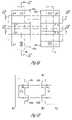
- FIG. 3is a partial top view of an NVDRAM array illustrating the formation of four adjacent NVDRAM cells having NFET transistors, and further illustrating bit line and word line representations superimposed on the array, according to various embodiments of the present subject matter.
- Active regions 340 and 342 for the switching transistorsare defined in a substrate.
- Four transistors 344 A, 344 B, 344 C, and 344 Dare capable of being formed in the illustrated active regions 340 and 342 .
- NFET transistorsare formed on a p-type substrate or well region.
- a gate insulator stack and a gateare formed at 344 A for transistor 302 A, at 344 B for transistor 302 B, at 344 C for transistor 302 C, and at 344 D for transistor 302 D.
- a metal silicide layeris formed to contact the substrate at 346 for transistors 302 A and 302 B, and at 348 for transistors 302 C and 302 D.
- the substrateis heavily doped with n-type impurities to form a first n+ diffusion region (or drain region) at 304 A for transistor 302 A, at 304 B for transistor 302 B, at 304 C for transistor 302 C, and at 304 D for transistor 302 D, and to form a second n+ diffusion region (or source or floating node region) at 306 A for transistor 302 A, at 306 B for transistor 302 B, at 306 C for transistor 302 C, and at 306 D for transistor 302 D.
- n-type impuritiesto form a first n+ diffusion region (or drain region) at 304 A for transistor 302 A, at 304 B for transistor 302 B, at 304 C for transistor 302 C, and at 304 D for transistor 302 D.
- Bit line contactsare shown at 354 A, 354 B, 354 C and 354 D for the bit lines (BL).
- Word lines (WL)contacts the gates.
- the metal-silicide layercontacts the p-type substrate, and thus forms Schottky diodes at 350 and 352 .
- Lateral semiconductor junction diodesare formed at the p-n+ junctions at 356 and 358 . In the illustrated array, adjacent memory cells share Schottky diodes and lateral junction diodes, and thus save space.
- the bit line contactscan be shared by adjacent memory cells as well.
- FIGS. 4A–4Dillustrate processes for fabricating the NVDRAM array of FIG. 3 , according to various embodiments of the present subject matter.
- transistor active regions 440 and 442are defined in a p-type substrate.
- a first layer of tunnel oxidee.g. SiO 2
- the first tunnel oxide layeris selectively removed at 446 for a desired storage node region.
- One of ordinary skill in the artwill understand, upon reading and comprehending this disclosure, that the Schottky diode and lateral junction diode will be formed at the desired storage node region 446 .
- a layer of metal-silicide(or transition-metal silicide) is deposited using the mask 460 .
- the metal silicidecontacts the substrate at 446 , and extends into the gate insulator stack region. However, an appropriate tolerance margin is used to prevent the metal silicide from extending beyond the gate insulator stack region into the area where the first diffusion region will be formed.
- a layer of metal oxide(or transition metal oxide) is deposited on the layer of metal silicide. This metal oxide functions as shallow charge traps to hold charge in the gate insulator stack.
- a second layer of tunnel oxideis formed on the metal oxide layer.
- a polysilicon layeris formed on the second layer of tunnel oxide, and a polysilicon gate is defined therein as represented by 462 and 464 in FIG. 4B .
- FIG. 4Balso illustrates the area 446 where the metal-silicide layer contacts the substrate.
- FIG. 4Cillustrates the outline of the block-mask 466 to define the asymmetric n+ diffusion at the source side of the device.
- the block mask 466defines the built-in Schottky diode, generally represented at region 418 , also defines the built-in lateral n+-p diode, generally represented at region 414 .
- Both the poly-silicon gate and diffusion channel regionsare silicided after the gate definition and n+ source/drain implant.
- the over-layer of the second silicideoverlaps the buried silicide and also connects the gate insulator stack.
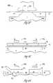
- FIG. 4Dillustrates a top view of the fabricated memory array. This top view serves as a point of reference for the cross-sectional views of FIGS. 4F–H .
- the NVDRAM of the present subject matteris capable of being formed using standard silicon gate FET device processes along with the following unique processes.
- One processrelates to forming the metal-silicide layer to form a Schottky body contact which provides the built-in Schottky diode.
- the first layer of gate oxidee.g. SiO 2
- a body contact maskremoves the oxide over the selected “source” region of p-substrate for the Schottky metal-silicide layer (e.g. ZrSi 2 ).
- the ZrSi 2 layeris formed or deposited.
- a metal oxidee.g. ZrO 2
- ALDatomic layer deposition
- the metal oxideis selectively defined to ensure appropriate overlap into the FET gate region. This definition of the metal oxide and underlayer ZrSi 2 plate requires a second additional mask.
- a layer of stoichiometric SiO 2 or Al 2 O 3is then deposited.
- the polysilicon gateis deposited and defined.
- a unique block maskdefines the source-drain n+ implant region while also implanting the polysilicon gate.
- all processing stepscould be those of standard CMOS or SOI-CMOS FET technology including those used for NiSi or CoSi 2 for forming a second silicide layer in the gate and channel regions.
- the second silicide layeroverlaps the first silicide layer in selected regions of the channel.
- FIG. 4Eis a schematic illustration of the NVDRAM array illustrated in FIGS. 3 and 4D according to various embodiments of the present subject matter.
- both diode 468 and diode 470represent a combination of a Schottky diode and a lateral p-n+ junction diode, such as is generally illustrated by diode 114 in FIG. 1C .
- transistors 402 A and 402 Bshare a Schottky diode and lateral junction diode represented by diode 468
- transistors 402 C and 402 Dshare a Schottky diode and lateral junction diode represented by diode 470 .
- FIG. 4Fillustrates a cross-sectional view taken along line 4 F— 4 F of FIG. 4D .
- the illustrated transistor 402 Aincludes a first diffusion region or drain region 404 A and a second diffusion region or source region 406 A formed in a substrate.
- a transistor gate 410 Ais separated from the substrate by a gate insulator stack.
- the illustrated gate insulator stackincludes a floating plate 412 , which includes a layer of metal silicide as represented by the dotted line.
- the floating plateis sandwiched between a first tunnel oxide and a second tunnel oxide in the gate insulator stack.
- a windowis formed in the first tunnel oxide such that, when the metal silicide layer 412 is deposited, it contacts the second diffusion region 406 A.
- This junction between the metal silicide layer and the second diffusion regionprovides the Schottky diode.
- Schottky barrier heights for metal or metal silicide-siliconp-type or n-type is capable of being varied by selecting an appropriate metal or metal-silicide to be a low barrier Schottky or a high barrier Schottky.
- the Schottky diodeis a majority carrier device, and thus has a very fast time constant. Additionally, the Schottky diode can be fabricated to have a very low reverse leakage ( ⁇ 1E-8 A/cm 2 ) while conducting a large forward current at a negligible voltage drop.
- FIG. 4Gillustrates a cross-sectional view taken along line 4 G— 4 G of FIG. 4D .
- the transistor active regions 440 and 442formed in a p-type substrate, and are separated by isolation regions.
- a first tunnel oxide layeris formed above the p-type substrate, a floating plate, including a metal silicide layer 412 , is formed above the first tunnel oxide layer, and a second tunnel oxide layer is formed above the floating plate.
- the word line (WL)includes a n+ doped polysilicon region 472 , which corresponds to the asymmetric n+ source/drain mask.
- Bit lines (BL)are formed above the word line (WL) as illustrated.
- FIG. 4Hillustrates a cross-sectional view taken along line 4 H— 4 H of FIG. 4D .
- the transistor active regions 440 and 442formed in a p-type substrate, and are separated by isolation regions.
- the asymmetric n+ source/drain maskprovides the illustrated doping profile in which both a p substrate and an n+ diffusion region share a top surface of the transistor active regions.
- the first tunnel oxideis selectively removed from the top surface at source or storage node region of the cell so that the metal silicide layer directly contacts both the p substrate and the n+ second diffusion region or source.
- a lateral semiconductor junction diodeis formed by the p-n+ junction as illustrated by diode 414 .
- junction between the n+ diffusion region and the metal silicideis an ohmic contact.
- a Schottky diodeis formed by the junction between the p substrate and the metal silicide as illustrated by diode 418 .
- Bit linesare formed above the transistor active regions as illustrated.
- FIG. 5Aillustrates a partial top view of an NVDRAM array illustrating the formation of four adjacent NVDRAM cell having PFET transistors according to various aspects of the present subject matter.
- charge polaritiesare reversed.
- the PFET cellis inherently slower than the NFET cell because holes are less mobile than electrons.
- the NFET cellhas advantages over the PFET cell.
- the basic concepts of the present subjectare valid for both NFET and PFET cells.
- One of ordinary skill in the artwill understand, upon reading and comprehending this disclosure, how to design both NFET and PFET cell embodiments.
- FIG. 5Bis a schematic illustration of the NVDRAM array illustrated in FIG. 5A according to various embodiments of the present subject matter.
- both diode 568 and diode 570represent a combination of a Schottky diode and a lateral p+-n junction diode.
- diode 568represents a Schottky diode and a lateral p+-n junction diode.
- adjacent transistors 502 A and 502 Bshare a Schottky diode and lateral junction diode represented by diode 568
- adjacent transistors 502 C and 502 Dshare a Schottky diode and lateral junction diode represented by diode 570 .
- FIG. 5Cillustrates a cross-sectional view taken along line 5 C— 5 C of FIG. 5A .
- the illustrated transistor 502 Aincludes a first diffusion region or drain region 504 A and a second diffusion region or source region 506 A formed in a substrate.
- a transistor gate 510 Ais separated from the substrate by a gate insulator stack.
- the illustrated gate insulator stackincludes a floating plate 512 , which includes a layer of metal silicide as represented by the dotted line.
- the floating plate 512is sandwiched between a first tunnel oxide and a second tunnel oxide in the gate insulator stack.
- a windowis formed in the first tunnel oxide such that, when the metal silicide layer is deposited, it contacts the second diffusion region. This junction between the metal silicide layer and the second diffusion region provides the Schottky diode
- FIG. 5Dillustrates a cross-sectional view taken along line 5 D— 5 D of FIG. 5A .
- the transistor active regionsare formed in an n-type substrate, and are separated by isolation regions.
- a first tunnel oxide layeris formed above the n-type substrate, a floating plate, including a metal silicide layer 512 , is formed above the first tunnel oxide layer, and a second tunnel oxide layer is formed above the floating plate.
- the word lineincludes a p+ doped polysilicon region 572 , which corresponds to the asymmetric p+ source/drain mask. Bit lines are formed above the word line as illustrated.
- FIG. 5Eillustrates a cross-sectional view taken along line 5 E— 5 E of FIG. 5A .
- the transistor active regionsare formed in an n-type substrate, and are separated by isolation regions.
- the asymmetric p+ source/drain maskprovides the illustrated doping profile in which both an n substrate and a p+ diffusion region share a top surface of the transistor active regions.
- the first tunnel oxideis selectively removed from the top surface at source or storage node region of the cell so that the metal silicide layer 512 directly contacts both the n substrate and the p+ second diffusion region or source.
- a lateral semiconductor junction diodeis formed by the p+-n junction as illustrated by diode 514 .
- the junction between the n+diffusion region and the metal silicideis an ohmic contact.
- a Schottky diodeis formed by the junction between the metal silicide and the n substrate as illustrated by diode 518 .
- Bit linesare formed above the transistor active regions as illustrated.
- Table 1illustrates cell operations in various embodiments for an NFET NVDRAM for which Vdd is approximately equal to 2.5 V.
- FIG. 6illustrates forward and reverse characteristics for the Schottky diode 618 and the lateral semiconductor junction diode 614 individually, and further illustrates the forward and reverse characteristics for the combination 619 of the Schottky diode and the lateral semiconductor junction diode.
- the difference in the characteristics of the parallel diodesare significant.
- the illustrated combined characteristics of the two diodesdefine the write/erase conditions and characteristics of the cell.
- FIG. 7is a high-level block diagram of an electronic system according to various embodiments of the present subject matter.
- the system 700is a computer system, a process control system or other system that employs a processor and associated memory.
- the electronic system 700has functional elements, including a processor or arithmetic/logic unit (ALU) 702 , a control unit 704 , a memory device unit 706 and an input/output (I/O) device 708 .
- ALUarithmetic/logic unit
- the control unit 704coordinates all operations of the processor 702 , the memory device 706 and the I/O devices 708 by continuously cycling through a set of operations that cause instructions to be fetched from the memory device 706 and executed.
- the memory device 706includes, but is not limited to, random access memory (RAM) devices, read-only memory (ROM) devices, and peripheral devices such as a floppy disk drive and a compact disk CD-ROM drive.
- RAMrandom access memory
- ROMread-only memory
- peripheral devicessuch as a floppy disk drive and a compact disk CD-ROM drive.
- FIG. 7The illustration of system, as shown in FIG. 7 , is intended to provide a general understanding of one application for the structure and circuitry of the present subject matter, and is not intended to serve as a complete description of all the elements and features of an electronic system using NVDRAM cells according to the present subject matter.
- an electronic systemcan be fabricated in single-package processing units, or even on a single semiconductor chip, in order to reduce the communication time between the processor and the memory device.
- Applications containing NVDRAM cellsinclude electronic systems for use in memory modules, device drivers, power modules, communication modems, processor modules, and application-specific modules, and may include multilayer, multichip modules.
- Such circuitrycan further be a subcomponent of a variety of electronic systems, such as a clock, a television, a cell phone, a personal computer, an automobile, an industrial control system, an aircraft, and others.
- FIG. 8is a simplified block diagram of a memory device according to various embodiments of the present subject matter.
- the illustrated memory device 806includes read/write control circuitry 880 to communicate with a memory array 882 of NVDRAM cells 884 A–D.
- the read/write control circuitry 880includes a word line select and power circuitry 886 to provide a pulse on a selected word line.
- the read/write control circuitry 880includes a bit line select and power circuitry 888 to provide a pulse on a selected bit line.
- the read/write control circuitry 880includes a body potential control circuitry 890 .
- the body control circuitryincludes selection circuitry to provide a pulse to a selected well.
- the read/write control circuitry 880includes read circuitry 892 to sense the state of the cell by detecting potential changes on the bit lines.
- the present subject matterrelates to a non-volatile memory cell.
- the memory cellincludes a switching transistor that is fabricated with a built-in floating plate in the gate insulator stack and at least one built-in diode.
- the floating plateis charged using a built-in lateral semiconductor junction diode when the cell is written.
- a forward biased Schottky diodeis used to discharge the floating plate. Programming the cell is fast, and does not require high voltage programming.
Landscapes
- Engineering & Computer Science (AREA)
- Microelectronics & Electronic Packaging (AREA)
- Semiconductor Memories (AREA)
Abstract
Description
| TABLE 1 | |||
| Node | |||
| potentials: | |||
| Bit | Word | Subst | Storage | ||
| Operation | Line | Line | rate | Node (S) | |
| Write | |||||
| 1 | +5 V | 2.5 V | 0 V | Float | Reverse biased diode. |
| (High) | Floating plate of the | ||||
| addressed bit is charged: | |||||
| VTChange: | |||||
| VT(0) −> VT(1) = 2.5 V | |||||
| Write 0 | 0 V | 0 V | 2.5 V | Float | Forward biased diode. |
| (Low) | Current (holes) neutralize | ||||
| charges of the addressed | |||||
| Bit: | |||||
| VTChange: | |||||
| VT(1) −> VT(0) = 1.0 V | |||||
| Half- | 0 V | 2.5 V | 0 V | Float | No change in state. |
| select | |||||
| cells | |||||
| Read 1 | Float | 2.5 V | 0 V | Float (1) | Device Off: No change in |
| Bit Line potential. | |||||
| Read 0 | Float | 2.5 V | 0 V | Float (0) | Device On: Change in Bit |
| Line potential sensed. | |||||
One of ordinary skill in the art will understand, upon reading and comprehending this disclosure, that other NVDRAM cell designs may require other cell operations.
Claims (35)
Priority Applications (2)
| Application Number | Priority Date | Filing Date | Title |
|---|---|---|---|
| US10/788,230US7130216B2 (en) | 2002-08-30 | 2004-02-26 | One-device non-volatile random access memory cell |
| US11/475,312US7485513B2 (en) | 2002-08-30 | 2006-06-27 | One-device non-volatile random access memory cell |
Applications Claiming Priority (2)
| Application Number | Priority Date | Filing Date | Title |
|---|---|---|---|
| US10/232,848US6903969B2 (en) | 2002-08-30 | 2002-08-30 | One-device non-volatile random access memory cell |
| US10/788,230US7130216B2 (en) | 2002-08-30 | 2004-02-26 | One-device non-volatile random access memory cell |
Related Parent Applications (1)
| Application Number | Title | Priority Date | Filing Date |
|---|---|---|---|
| US10/232,848DivisionUS6903969B2 (en) | 2002-08-30 | 2002-08-30 | One-device non-volatile random access memory cell |
Related Child Applications (1)
| Application Number | Title | Priority Date | Filing Date |
|---|---|---|---|
| US11/475,312DivisionUS7485513B2 (en) | 2002-08-30 | 2006-06-27 | One-device non-volatile random access memory cell |
Publications (2)
| Publication Number | Publication Date |
|---|---|
| US20040160825A1 US20040160825A1 (en) | 2004-08-19 |
| US7130216B2true US7130216B2 (en) | 2006-10-31 |
Family
ID=31977091
Family Applications (3)
| Application Number | Title | Priority Date | Filing Date |
|---|---|---|---|
| US10/232,848Expired - LifetimeUS6903969B2 (en) | 2002-08-30 | 2002-08-30 | One-device non-volatile random access memory cell |
| US10/788,230Expired - LifetimeUS7130216B2 (en) | 2002-08-30 | 2004-02-26 | One-device non-volatile random access memory cell |
| US11/475,312Expired - LifetimeUS7485513B2 (en) | 2002-08-30 | 2006-06-27 | One-device non-volatile random access memory cell |
Family Applications Before (1)
| Application Number | Title | Priority Date | Filing Date |
|---|---|---|---|
| US10/232,848Expired - LifetimeUS6903969B2 (en) | 2002-08-30 | 2002-08-30 | One-device non-volatile random access memory cell |
Family Applications After (1)
| Application Number | Title | Priority Date | Filing Date |
|---|---|---|---|
| US11/475,312Expired - LifetimeUS7485513B2 (en) | 2002-08-30 | 2006-06-27 | One-device non-volatile random access memory cell |
Country Status (1)
| Country | Link |
|---|---|
| US (3) | US6903969B2 (en) |
Cited By (15)
| Publication number | Priority date | Publication date | Assignee | Title |
|---|---|---|---|---|
| US7485513B2 (en) | 2002-08-30 | 2009-02-03 | Micron Technology, Inc. | One-device non-volatile random access memory cell |
| US20090168529A1 (en)* | 2007-12-26 | 2009-07-02 | Sanyo Electric Co., Ltd. | Nonvolatile semiconductor memory device, method for manufacturing the same, and nonvolatile memory array |
| US20090302369A1 (en)* | 2008-06-05 | 2009-12-10 | Supratik Guha | Method and apparatus for flatband voltage tuning of high-k field effect transistors |
| US7728626B2 (en) | 2002-07-08 | 2010-06-01 | Micron Technology, Inc. | Memory utilizing oxide nanolaminates |
| US8576607B1 (en)* | 2010-07-02 | 2013-11-05 | Farid Nemati | Hybrid memory cell array and operations thereof |
| US10153039B1 (en) | 2017-07-05 | 2018-12-11 | Micron Technology, Inc. | Memory cells programmed via multi-mechanism charge transports |
| US10153381B1 (en) | 2017-07-05 | 2018-12-11 | Micron Technology, Inc. | Memory cells having an access gate and a control gate and dielectric stacks above and below the access gate |
| US10153348B1 (en) | 2017-07-05 | 2018-12-11 | Micron Technology, Inc. | Memory configurations |
| US10176870B1 (en) | 2017-07-05 | 2019-01-08 | Micron Technology, Inc. | Multifunctional memory cells |
| US10262736B2 (en) | 2017-07-05 | 2019-04-16 | Micron Technology, Inc. | Multifunctional memory cells |
| US10276576B2 (en) | 2017-07-05 | 2019-04-30 | Micron Technology, Inc. | Gated diode memory cells |
| US10297493B2 (en) | 2017-07-05 | 2019-05-21 | Micron Technology, Inc. | Trench isolation interfaces |
| US10374101B2 (en) | 2017-07-05 | 2019-08-06 | Micron Technology, Inc. | Memory arrays |
| US10411026B2 (en) | 2017-07-05 | 2019-09-10 | Micron Technology, Inc. | Integrated computing structures formed on silicon |
| US10892340B2 (en) | 2017-07-05 | 2021-01-12 | Micron Technology, Inc. | Memory cell structures |
Families Citing this family (45)
| Publication number | Priority date | Publication date | Assignee | Title |
|---|---|---|---|---|
| US6759257B2 (en)* | 2001-11-13 | 2004-07-06 | Fujitsu Limited | Structure and method for embedding capacitors in z-connected multi-chip modules |
| US6784480B2 (en)* | 2002-02-12 | 2004-08-31 | Micron Technology, Inc. | Asymmetric band-gap engineered nonvolatile memory device |
| EP1357603A3 (en)* | 2002-04-18 | 2004-01-14 | Innovative Silicon SA | Semiconductor device |
| EP1355316B1 (en)* | 2002-04-18 | 2007-02-21 | Innovative Silicon SA | Data storage device and refreshing method for use with such device |
| US6917078B2 (en)* | 2002-08-30 | 2005-07-12 | Micron Technology Inc. | One transistor SOI non-volatile random access memory cell |
| US6888200B2 (en)* | 2002-08-30 | 2005-05-03 | Micron Technology Inc. | One transistor SOI non-volatile random access memory cell |
| US7042027B2 (en)* | 2002-08-30 | 2006-05-09 | Micron Technology, Inc. | Gated lateral thyristor-based random access memory cell (GLTRAM) |
| JP4385834B2 (en)* | 2003-04-15 | 2009-12-16 | パナソニック株式会社 | Routing control method and router apparatus |
| US7085153B2 (en)* | 2003-05-13 | 2006-08-01 | Innovative Silicon S.A. | Semiconductor memory cell, array, architecture and device, and method of operating same |
| US6912150B2 (en)* | 2003-05-13 | 2005-06-28 | Lionel Portman | Reference current generator, and method of programming, adjusting and/or operating same |
| US20040228168A1 (en)* | 2003-05-13 | 2004-11-18 | Richard Ferrant | Semiconductor memory device and method of operating same |
| US8125003B2 (en)* | 2003-07-02 | 2012-02-28 | Micron Technology, Inc. | High-performance one-transistor memory cell |
| US7184298B2 (en)* | 2003-09-24 | 2007-02-27 | Innovative Silicon S.A. | Low power programming technique for a floating body memory transistor, memory cell, and memory array |
| US6984862B2 (en)* | 2003-10-20 | 2006-01-10 | Hewlett-Packard Development Company, L.P. | Storage device with charge trapping structure and methods |
| KR100591254B1 (en)* | 2004-04-29 | 2006-06-19 | 엘지.필립스 엘시디 주식회사 | Organic EL device and method of manufacturing the same |
| US20050275106A1 (en)* | 2004-06-14 | 2005-12-15 | Fricke Peter J | Electronic isolation device |
| US7279740B2 (en) | 2005-05-12 | 2007-10-09 | Micron Technology, Inc. | Band-engineered multi-gated non-volatile memory device with enhanced attributes |
| US7402850B2 (en)* | 2005-06-21 | 2008-07-22 | Micron Technology, Inc. | Back-side trapped non-volatile memory device |
| US7829938B2 (en)* | 2005-07-14 | 2010-11-09 | Micron Technology, Inc. | High density NAND non-volatile memory device |
| US7429767B2 (en)* | 2005-09-01 | 2008-09-30 | Micron Technology, Inc. | High performance multi-level non-volatile memory device |
| KR100695164B1 (en)* | 2005-11-09 | 2007-03-14 | 삼성전자주식회사 | Hybrid type nonvolatile memory device including transistor and diode as switching device |
| US7855414B2 (en)* | 2006-07-28 | 2010-12-21 | Broadcom Corporation | Semiconductor device with increased breakdown voltage |
| JP4364227B2 (en)* | 2006-09-29 | 2009-11-11 | 株式会社東芝 | Semiconductor memory device |
| US7608898B2 (en)* | 2006-10-31 | 2009-10-27 | Freescale Semiconductor, Inc. | One transistor DRAM cell structure |
| US8547756B2 (en) | 2010-10-04 | 2013-10-01 | Zeno Semiconductor, Inc. | Semiconductor memory device having an electrically floating body transistor |
| US7760548B2 (en) | 2006-11-29 | 2010-07-20 | Yuniarto Widjaja | Semiconductor memory having both volatile and non-volatile functionality and method of operating |
| KR20090011886A (en)* | 2007-07-27 | 2009-02-02 | 삼성전자주식회사 | Capacitorless DRAM and its manufacture and operation method |
| US20100027355A1 (en)* | 2007-07-31 | 2010-02-04 | Dao Thuy B | Planar double gate transistor storage cell |
| US8320191B2 (en) | 2007-08-30 | 2012-11-27 | Infineon Technologies Ag | Memory cell arrangement, method for controlling a memory cell, memory array and electronic device |
| US8207582B2 (en)* | 2009-01-05 | 2012-06-26 | Micron Technology, Inc. | Semiconductor devices including dual gate structures |
| US8193062B2 (en)* | 2009-09-25 | 2012-06-05 | International Business Machines Corporation | Asymmetric silicon-on-insulator SRAM cell |
| CN101777586B (en)* | 2010-01-21 | 2012-11-21 | 复旦大学 | Hybrid junction source/drain field effect transistor and preparation method thereof |
| US8283722B2 (en) | 2010-06-14 | 2012-10-09 | Broadcom Corporation | Semiconductor device having an enhanced well region |
| US8228730B2 (en) | 2010-08-31 | 2012-07-24 | Micron Technology, Inc. | Memory cell structures and methods |
| US9123807B2 (en)* | 2010-12-28 | 2015-09-01 | Broadcom Corporation | Reduction of parasitic capacitance in a semiconductor device |
| US9492678B2 (en)* | 2011-07-14 | 2016-11-15 | Cyberonics, Inc. | Far field radiative powering of implantable medical therapy delivery devices |
| US8989867B2 (en) | 2011-07-14 | 2015-03-24 | Cyberonics, Inc. | Implantable nerve wrap for nerve stimulation configured for far field radiative powering |
| US8514626B2 (en) | 2011-07-26 | 2013-08-20 | Micron Technology, Inc. | Memory cells and methods of storing information |
| KR101982141B1 (en)* | 2013-01-04 | 2019-05-27 | 한국전자통신연구원 | Eeprom cell and eeprom apparatus |
| TWI570738B (en) | 2013-03-29 | 2017-02-11 | 萬國商業機器公司 | A primary memory module with a record of usage history and applications of the primary memory module to a computer system |
| CN105336622B (en)* | 2014-07-30 | 2018-09-07 | 中芯国际集成电路制造(上海)有限公司 | Half floating-gate device and forming method thereof |
| CN104183594B (en)* | 2014-08-17 | 2017-01-25 | 复旦大学 | Gallium nitride power device with semi-floating-gate structure |
| KR102324627B1 (en) | 2014-10-31 | 2021-11-10 | 삼성전자주식회사 | Semiconductor device having magneto-resistive device |
| US11069742B2 (en) | 2019-11-23 | 2021-07-20 | Tetramem Inc. | Crossbar array circuit with parallel grounding lines |
| CN111540740B (en)* | 2020-05-13 | 2022-06-21 | 复旦大学 | Semi-floating gate memory based on pn junction and Schottky diode and method of making the same |
Citations (31)
| Publication number | Priority date | Publication date | Assignee | Title |
|---|---|---|---|---|
| US3918033A (en) | 1974-11-11 | 1975-11-04 | Ibm | SCR memory cell |
| US3964085A (en) | 1975-08-18 | 1976-06-15 | Bell Telephone Laboratories, Incorporated | Method for fabricating multilayer insulator-semiconductor memory apparatus |
| US3978577A (en) | 1975-06-30 | 1976-09-07 | International Business Machines Corporation | Fixed and variable threshold N-channel MNOSFET integration technique |
| US4488262A (en) | 1981-06-25 | 1984-12-11 | International Business Machines Corporation | Electronically programmable read only memory |
| JPS61166078A (en) | 1985-01-17 | 1986-07-26 | Matsushita Electronics Corp | Floating gate type non-volatile memory device |
| US4791604A (en) | 1984-02-15 | 1988-12-13 | Joseph J. Bednarz | Sheet random access memory |
| US4829482A (en) | 1985-10-18 | 1989-05-09 | Xicor, Inc. | Current metering apparatus for optimally inducing field emission of electrons in tunneling devices and the like |
| US4870470A (en) | 1987-10-16 | 1989-09-26 | International Business Machines Corporation | Non-volatile memory cell having Si rich silicon nitride charge trapping layer |
| US5043946A (en) | 1988-02-09 | 1991-08-27 | Sharp Kabushiki Kaisha | Semiconductor memory device |
| US5557569A (en) | 1993-10-12 | 1996-09-17 | Texas Instruments Incorporated | Low voltage flash EEPROM C-cell using fowler-nordheim tunneling |
| US5621683A (en) | 1994-12-06 | 1997-04-15 | U.S. Philips Corporation | Semiconductor memory with non-volatile memory transistor |
| US5801993A (en) | 1996-10-01 | 1998-09-01 | Lg Semicon Co., Ltd. | Nonvolatile memory device |
| US5825064A (en)* | 1919-03-10 | 1998-10-20 | Agency Of Industrial Science And Technology And Seiko Instruments Inc. | Semiconductor volatile/nonvolatile memory |
| US5963476A (en) | 1996-09-05 | 1999-10-05 | Macronix International Co., Ltd. | Fowler-Nordheim (F-N) tunneling for pre-programming in a floating gate memory device |
| US5981335A (en) | 1997-11-20 | 1999-11-09 | Vanguard International Semiconductor Corporation | Method of making stacked gate memory cell structure |
| US6104045A (en) | 1998-05-13 | 2000-08-15 | Micron Technology, Inc. | High density planar SRAM cell using bipolar latch-up and gated diode breakdown |
| US6172397B1 (en) | 1995-06-15 | 2001-01-09 | Mitsubishi Denki Kabushiki Kaisha | Non-volatile semiconductor memory device |
| US6201734B1 (en) | 1998-09-25 | 2001-03-13 | Sandisk Corporation | Programmable impedance device |
| US6462359B1 (en) | 2001-03-22 | 2002-10-08 | T-Ram, Inc. | Stability in thyristor-based memory device |
| US20030042534A1 (en) | 2001-08-30 | 2003-03-06 | Micron Technology, Inc. | Scalable flash/NV structures and devices with extended endurance |
| US6545297B1 (en) | 1998-05-13 | 2003-04-08 | Micron Technology, Inc. | High density vertical SRAM cell using bipolar latchup induced by gated diode breakdown |
| US20030072126A1 (en) | 2001-08-30 | 2003-04-17 | Micron Technology, Inc. | Decoupling capacitor for high frequency noise immunity |
| US20030089942A1 (en) | 2001-11-09 | 2003-05-15 | Micron Technology, Inc. | Scalable gate and storage dielectric |
| US6600188B1 (en) | 2001-06-25 | 2003-07-29 | Lattice Semiconductor Corporation | EEPROM with a neutralized doping at tunnel window edge |
| US20030151948A1 (en) | 2002-02-12 | 2003-08-14 | Micron Technology, Inc. | Asymmetric band-gap engineered nonvolatile memory device |
| US6653174B1 (en) | 1998-06-05 | 2003-11-25 | T-Ram, Inc. | Thyristor-based device over substrate surface |
| US6674138B1 (en) | 2001-12-31 | 2004-01-06 | Advanced Micro Devices, Inc. | Use of high-k dielectric materials in modified ONO structure for semiconductor devices |
| US20040014304A1 (en) | 2002-07-18 | 2004-01-22 | Micron Technology, Inc. | Stable PD-SOI devices and methods |
| US6740928B2 (en) | 1999-06-04 | 2004-05-25 | Matsushita Electric Industrial Co., Ltd. | Semiconductor device |
| US6778441B2 (en) | 2001-08-30 | 2004-08-17 | Micron Technology, Inc. | Integrated circuit memory device and method |
| US6903969B2 (en)* | 2002-08-30 | 2005-06-07 | Micron Technology Inc. | One-device non-volatile random access memory cell |
Family Cites Families (16)
| Publication number | Priority date | Publication date | Assignee | Title |
|---|---|---|---|---|
| US981335A (en)* | 1908-09-21 | 1911-01-10 | Calvin W Vaughn | Safety device for die-holders. |
| US4670470A (en)* | 1979-08-15 | 1987-06-02 | Merck & Co., Inc. | Allylsulfoxide enzyme inhibitors |
| US5017977A (en) | 1985-03-26 | 1991-05-21 | Texas Instruments Incorporated | Dual EPROM cells on trench walls with virtual ground buried bit lines |
| US4828482A (en)* | 1985-08-06 | 1989-05-09 | The Babcock & Wilcox Company | A method of operating a fluid bed combustor |
| JP3321899B2 (en) | 1992-12-04 | 2002-09-09 | 株式会社デンソー | Semiconductor device |
| US5856943A (en)* | 1996-03-18 | 1999-01-05 | Integrated Memory Technologies, Inc. | Scalable flash EEPROM memory cell and array |
| US6768165B1 (en)* | 1997-08-01 | 2004-07-27 | Saifun Semiconductors Ltd. | Two bit non-volatile electrically erasable and programmable semiconductor memory cell utilizing asymmetrical charge trapping |
| US6445032B1 (en) | 1998-05-04 | 2002-09-03 | International Business Machines Corporation | Floating back gate electrically erasable programmable read-only memory(EEPROM) |
| TW480736B (en)* | 1999-06-24 | 2002-03-21 | Taiwan Semiconductor Mfg | Program and erase method of flash memory |
| US6754104B2 (en) | 2000-06-22 | 2004-06-22 | Progressant Technologies, Inc. | Insulated-gate field-effect transistor integrated with negative differential resistance (NDR) FET |
| AU2002251690A1 (en) | 2000-12-13 | 2002-08-12 | Rochester Institute Of Technology | A method and system for electrostatic bonding |
| CN1187839C (en)* | 2001-01-19 | 2005-02-02 | 三菱电机株式会社 | Semiconductor device |
| TW476144B (en) | 2001-02-02 | 2002-02-11 | Macronix Int Co Ltd | Non-volatile memory |
| US20030121948A1 (en)* | 2001-12-31 | 2003-07-03 | Hsien Chen Ming | Device for disabling shooting when nails runs out in a pneumatic nailer |
| JP2004039965A (en) | 2002-07-05 | 2004-02-05 | Renesas Technology Corp | Nonvolatile semiconductor memory device |
| US7221586B2 (en) | 2002-07-08 | 2007-05-22 | Micron Technology, Inc. | Memory utilizing oxide nanolaminates |
- 2002
- 2002-08-30USUS10/232,848patent/US6903969B2/ennot_activeExpired - Lifetime
- 2004
- 2004-02-26USUS10/788,230patent/US7130216B2/ennot_activeExpired - Lifetime
- 2006
- 2006-06-27USUS11/475,312patent/US7485513B2/ennot_activeExpired - Lifetime
Patent Citations (33)
| Publication number | Priority date | Publication date | Assignee | Title |
|---|---|---|---|---|
| US5825064A (en)* | 1919-03-10 | 1998-10-20 | Agency Of Industrial Science And Technology And Seiko Instruments Inc. | Semiconductor volatile/nonvolatile memory |
| US3918033A (en) | 1974-11-11 | 1975-11-04 | Ibm | SCR memory cell |
| US3978577A (en) | 1975-06-30 | 1976-09-07 | International Business Machines Corporation | Fixed and variable threshold N-channel MNOSFET integration technique |
| US3964085A (en) | 1975-08-18 | 1976-06-15 | Bell Telephone Laboratories, Incorporated | Method for fabricating multilayer insulator-semiconductor memory apparatus |
| US4488262A (en) | 1981-06-25 | 1984-12-11 | International Business Machines Corporation | Electronically programmable read only memory |
| US4791604A (en) | 1984-02-15 | 1988-12-13 | Joseph J. Bednarz | Sheet random access memory |
| JPS61166078A (en) | 1985-01-17 | 1986-07-26 | Matsushita Electronics Corp | Floating gate type non-volatile memory device |
| US4829482A (en) | 1985-10-18 | 1989-05-09 | Xicor, Inc. | Current metering apparatus for optimally inducing field emission of electrons in tunneling devices and the like |
| US4870470A (en) | 1987-10-16 | 1989-09-26 | International Business Machines Corporation | Non-volatile memory cell having Si rich silicon nitride charge trapping layer |
| US5043946A (en) | 1988-02-09 | 1991-08-27 | Sharp Kabushiki Kaisha | Semiconductor memory device |
| US5557569A (en) | 1993-10-12 | 1996-09-17 | Texas Instruments Incorporated | Low voltage flash EEPROM C-cell using fowler-nordheim tunneling |
| US5621683A (en) | 1994-12-06 | 1997-04-15 | U.S. Philips Corporation | Semiconductor memory with non-volatile memory transistor |
| US6172397B1 (en) | 1995-06-15 | 2001-01-09 | Mitsubishi Denki Kabushiki Kaisha | Non-volatile semiconductor memory device |
| US5963476A (en) | 1996-09-05 | 1999-10-05 | Macronix International Co., Ltd. | Fowler-Nordheim (F-N) tunneling for pre-programming in a floating gate memory device |
| US5801993A (en) | 1996-10-01 | 1998-09-01 | Lg Semicon Co., Ltd. | Nonvolatile memory device |
| US5981335A (en) | 1997-11-20 | 1999-11-09 | Vanguard International Semiconductor Corporation | Method of making stacked gate memory cell structure |
| US6104045A (en) | 1998-05-13 | 2000-08-15 | Micron Technology, Inc. | High density planar SRAM cell using bipolar latch-up and gated diode breakdown |
| US6545297B1 (en) | 1998-05-13 | 2003-04-08 | Micron Technology, Inc. | High density vertical SRAM cell using bipolar latchup induced by gated diode breakdown |
| US6653174B1 (en) | 1998-06-05 | 2003-11-25 | T-Ram, Inc. | Thyristor-based device over substrate surface |
| US6201734B1 (en) | 1998-09-25 | 2001-03-13 | Sandisk Corporation | Programmable impedance device |
| US6740928B2 (en) | 1999-06-04 | 2004-05-25 | Matsushita Electric Industrial Co., Ltd. | Semiconductor device |
| US6462359B1 (en) | 2001-03-22 | 2002-10-08 | T-Ram, Inc. | Stability in thyristor-based memory device |
| US6653175B1 (en) | 2001-03-22 | 2003-11-25 | T-Ram, Inc. | Stability in thyristor-based memory device |
| US6600188B1 (en) | 2001-06-25 | 2003-07-29 | Lattice Semiconductor Corporation | EEPROM with a neutralized doping at tunnel window edge |
| US20030072126A1 (en) | 2001-08-30 | 2003-04-17 | Micron Technology, Inc. | Decoupling capacitor for high frequency noise immunity |
| US20030042534A1 (en) | 2001-08-30 | 2003-03-06 | Micron Technology, Inc. | Scalable flash/NV structures and devices with extended endurance |
| US6778441B2 (en) | 2001-08-30 | 2004-08-17 | Micron Technology, Inc. | Integrated circuit memory device and method |
| US20030160277A1 (en) | 2001-11-09 | 2003-08-28 | Micron Technology, Inc. | Scalable gate and storage dielectric |
| US20030089942A1 (en) | 2001-11-09 | 2003-05-15 | Micron Technology, Inc. | Scalable gate and storage dielectric |
| US6674138B1 (en) | 2001-12-31 | 2004-01-06 | Advanced Micro Devices, Inc. | Use of high-k dielectric materials in modified ONO structure for semiconductor devices |
| US20030151948A1 (en) | 2002-02-12 | 2003-08-14 | Micron Technology, Inc. | Asymmetric band-gap engineered nonvolatile memory device |
| US20040014304A1 (en) | 2002-07-18 | 2004-01-22 | Micron Technology, Inc. | Stable PD-SOI devices and methods |
| US6903969B2 (en)* | 2002-08-30 | 2005-06-07 | Micron Technology Inc. | One-device non-volatile random access memory cell |
Non-Patent Citations (19)
| Title |
|---|
| Bauer, F , et al., "Design aspects of MOS controlled thyristor elements", International Electron Devices Meeting 1989. Technical Digest, (1989),297-300. |
| Bhattacharyya, A. , "Physical & Electrical Characteristics of LPCVD Silicon Rich Nitride", ECS Technical Digest, J. Electrochem. Soc., 131(11), 691 RDP, New Orleans,(1984),469C. |
| Carter, R J., "Electrical Characterization of High-k Materials Prepared By Atomic Layer CVD", IWGI, (2001),94-99. |
| Chang, H R., et al., "MOS trench gate field-controlled thyristor", Technical Digest-International Electron Devices Meeting, (1989),293-296. |
| Choi, J D., et al., "A0.15 um NAND Flash Technology with ).11 um2 cell Size for 1 Gbit Flash Memory", IEDM Technical Digest, (2000),767-770. |
| Frohman-Bentchkowsky, D , "An Integrated metal-nitride-oxide-silicon (MNOS) memory", Proceedings of the IEEE, 57(6), (Jun. 1969),1190-1192. |
| Han, Kwangseok , "Characteristics of P-Channel Si Nano-Crystal Memory", IEDM Technical Digest, International Electron Devices Meeting, (Dec. 10-13, 2000),309-312. |
| Jagar, S , "Single grain thin-film transistor (TFT) with SOI CMOS performance formed by metal-induced-lateral-crystallization", International Electron Devices Meeting 1999. Technical Digest, (1999),293-6. |
| Kumar, M. J., "Lateral Schottky Rectifiers for Power Integrated Circuits", International Workshop on the Physics of Semiconductor Devices, 11th, 4746, Allied Publishers Ltd., New Delhi, India,(2002),414-421. |
| Lai, S K., et al., "Comparison and trends in Today's dominant E2 Technologies", IEDM Technical Digest, (1986),580-583. |
| Nemati, F , et al., "A novel high density, low voltage SRAM cell with a vertical NDR device", 1998 Symposium on VLSI Technology Digest of Technical Papers, (1998),66-7. |
| Nemati, F , et al., "A Novel thyristor-based SRAM cell (T-RAM) for high-speed, low-voltage, giga-scale memories", International Electron Devices Meeting 1999. Technical Digest, (1999),283-6. |
| Ohsawa, T , "Memory design using one-transistor gain cell on SOI", IEEE International Solid-State Circuits Conference. Digest of Technical Papers, vol. 1, (2002),152-455. |
| Okhonin, S , "A SOI capacitor-less 1T-DRAM concept", 2001 IEEE International SOI Conference Proceedings, IEEE. 2001, (2000),153-4. |
| Shinohe, T , et al., "Ultra-high di/dt 2500 V MOS assisted gate-triggered thyristors (MAGTs) for high repetition excimer laser system", International Electron Devices Meeting 1989. Technical Digest, (1989),301-4. |
| Sze, S. M., "Table 3: Measured Schottky Barrier Heights", In: Physics of Semiconductor Devices, John Wiley & Sons, Inc.,(1981),p. 291. |
| Tiwari, Sandip , "Volatile and Non-Volatile Memories in Silicon with Nano-Crystal Storage", Int'l Electron Devices Meeting: Technical Digest, Washington, DC,(Dec. 1995),521-524. |
| Van Meer, H , "Ultra-thin film fully-depleted SOI CMOS with raised G/S/D device architecture for sub-100 nm applications", 2001 IEEE International SOI Conference, (2001),45-6. |
| Zhang, H. , "Atomic Layer Deposition of High Dielectric Constant Nanolaminates", Journal of The Electrochemical Society, 148(4), (Apr. 2001),F63-F66. |
Cited By (33)
| Publication number | Priority date | Publication date | Assignee | Title |
|---|---|---|---|---|
| US7728626B2 (en) | 2002-07-08 | 2010-06-01 | Micron Technology, Inc. | Memory utilizing oxide nanolaminates |
| US8228725B2 (en) | 2002-07-08 | 2012-07-24 | Micron Technology, Inc. | Memory utilizing oxide nanolaminates |
| US7485513B2 (en) | 2002-08-30 | 2009-02-03 | Micron Technology, Inc. | One-device non-volatile random access memory cell |
| US20090168529A1 (en)* | 2007-12-26 | 2009-07-02 | Sanyo Electric Co., Ltd. | Nonvolatile semiconductor memory device, method for manufacturing the same, and nonvolatile memory array |
| US8189385B2 (en)* | 2007-12-26 | 2012-05-29 | Semiconductor Components Industries, Llc | Nonvolatile semiconductor memory device, method for manufacturing the same, and nonvolatile memory array |
| US20090302369A1 (en)* | 2008-06-05 | 2009-12-10 | Supratik Guha | Method and apparatus for flatband voltage tuning of high-k field effect transistors |
| US7821081B2 (en)* | 2008-06-05 | 2010-10-26 | International Business Machines Corporation | Method and apparatus for flatband voltage tuning of high-k field effect transistors |
| US8658501B2 (en) | 2008-06-05 | 2014-02-25 | International Business Machines Corporation | Method and apparatus for flatband voltage tuning of high-k field effect transistors |
| US8576607B1 (en)* | 2010-07-02 | 2013-11-05 | Farid Nemati | Hybrid memory cell array and operations thereof |
| US10374101B2 (en) | 2017-07-05 | 2019-08-06 | Micron Technology, Inc. | Memory arrays |
| US10546639B2 (en) | 2017-07-05 | 2020-01-28 | Micron Technology, Inc. | Multifunctional memory cells |
| US10153348B1 (en) | 2017-07-05 | 2018-12-11 | Micron Technology, Inc. | Memory configurations |
| US10176870B1 (en) | 2017-07-05 | 2019-01-08 | Micron Technology, Inc. | Multifunctional memory cells |
| US10262736B2 (en) | 2017-07-05 | 2019-04-16 | Micron Technology, Inc. | Multifunctional memory cells |
| US10276576B2 (en) | 2017-07-05 | 2019-04-30 | Micron Technology, Inc. | Gated diode memory cells |
| US10297493B2 (en) | 2017-07-05 | 2019-05-21 | Micron Technology, Inc. | Trench isolation interfaces |
| US10153039B1 (en) | 2017-07-05 | 2018-12-11 | Micron Technology, Inc. | Memory cells programmed via multi-mechanism charge transports |
| US10411026B2 (en) | 2017-07-05 | 2019-09-10 | Micron Technology, Inc. | Integrated computing structures formed on silicon |
| US10483155B2 (en) | 2017-07-05 | 2019-11-19 | Micron Technology, Inc. | Trench isolation interfaces |
| US10541027B2 (en) | 2017-07-05 | 2020-01-21 | Micron Technology, Inc. | Multifunctional memory cells |
| US10153381B1 (en) | 2017-07-05 | 2018-12-11 | Micron Technology, Inc. | Memory cells having an access gate and a control gate and dielectric stacks above and below the access gate |
| US10566053B2 (en) | 2017-07-05 | 2020-02-18 | Micron Technology, Inc. | Memory cells programmed via multi-mechanism charge transports |
| US10741658B2 (en) | 2017-07-05 | 2020-08-11 | Micron Technology, Inc. | Memory configurations |
| US10797053B2 (en) | 2017-07-05 | 2020-10-06 | Micron Technology, Inc. | Gated diode memory cells |
| US10811424B2 (en) | 2017-07-05 | 2020-10-20 | Micron Technology, Inc. | Integrated computing structures formed on silicon |
| US10892340B2 (en) | 2017-07-05 | 2021-01-12 | Micron Technology, Inc. | Memory cell structures |
| US10957389B2 (en) | 2017-07-05 | 2021-03-23 | Micron Technology, Inc. | Multifunctional memory cells |
| US10998042B2 (en) | 2017-07-05 | 2021-05-04 | Micron Technology, Inc. | Memory cells with tunneling materials including lanthanum oxide |
| US11031283B2 (en) | 2017-07-05 | 2021-06-08 | Micron Technology, Inc. | Trench isolation interfaces |
| US11087842B2 (en) | 2017-07-05 | 2021-08-10 | Micron Technology, Inc. | Multifunctional memory cells |
| US11211503B2 (en) | 2017-07-05 | 2021-12-28 | Micron Technology, Inc. | Memory arrays |
| US11211124B2 (en) | 2017-07-05 | 2021-12-28 | Micron Technology, Inc. | Multifunctional memory cells |
| US11264472B2 (en) | 2017-07-05 | 2022-03-01 | Micron Technology, Inc. | Memory configurations |
Also Published As
| Publication number | Publication date |
|---|---|
| US20060240653A1 (en) | 2006-10-26 |
| US20040042268A1 (en) | 2004-03-04 |
| US7485513B2 (en) | 2009-02-03 |
| US20040160825A1 (en) | 2004-08-19 |
| US6903969B2 (en) | 2005-06-07 |
Similar Documents
| Publication | Publication Date | Title |
|---|---|---|
| US7130216B2 (en) | One-device non-volatile random access memory cell | |
| US7566601B2 (en) | Method of making a one transistor SOI non-volatile random access memory cell | |
| KR100254006B1 (en) | Semiconductor memory device | |
| US7312499B2 (en) | Semiconductor storage device and manufacturing method therefor, semiconductor device, portable electronic equipment and IC card | |
| US6388293B1 (en) | Nonvolatile memory cell, operating method of the same and nonvolatile memory array | |
| US7157773B2 (en) | Nonvolatile semiconductor memory device | |
| US20090101961A1 (en) | Memory devices with split gate and blocking layer | |
| US20040041206A1 (en) | One transistor SOI non-volatile random access memory cell | |
| US20020149061A1 (en) | Nonvolatile memory cell, operating method of the same and nonvolatile memory array | |
| US20060131642A1 (en) | Semiconductor storage | |
| US6801456B1 (en) | Method for programming, erasing and reading a flash memory cell | |
| US7544993B2 (en) | Semiconductor storage device and portable electronic equipment | |
| CN101221987A (en) | Non-volatile memory cell with polysilicon multi-layer insulation structure | |
| US7315060B2 (en) | Semiconductor storage device, manufacturing method therefor and portable electronic equipment | |
| US20090184359A1 (en) | Split-gate non-volatile memory devices having nitride tunneling layers | |
| EP1408511A1 (en) | Single bit nonvolatile memory cell and methods for programming and erasing thereof | |
| EP0443515B1 (en) | Nonvolatile semiconductor device | |
| US7816725B2 (en) | Semiconductor devices and methods of fabricating the same | |
| JP2004342889A (en) | Semiconductor storage device, semiconductor device, method of manufacturing semiconductor storage device, and portable electronic device | |
| US5589700A (en) | Semiconductor nonvolatile memory | |
| US7123518B2 (en) | Memory device | |
| US20060220096A1 (en) | Tunneling-enhanced floating gate semiconductor device | |
| JP3186209B2 (en) | How to use semiconductor devices | |
| JP2000349172A (en) | Semiconductor memory cell | |
| JPH0555600A (en) | Semiconductor nonvolatile memory device |
Legal Events
| Date | Code | Title | Description |
|---|---|---|---|
| FEPP | Fee payment procedure | Free format text:PAYOR NUMBER ASSIGNED (ORIGINAL EVENT CODE: ASPN); ENTITY STATUS OF PATENT OWNER: LARGE ENTITY | |
| STCF | Information on status: patent grant | Free format text:PATENTED CASE | |
| CC | Certificate of correction | ||
| FPAY | Fee payment | Year of fee payment:4 | |
| FPAY | Fee payment | Year of fee payment:8 | |
| AS | Assignment | Owner name:U.S. BANK NATIONAL ASSOCIATION, AS COLLATERAL AGENT, CALIFORNIA Free format text:SECURITY INTEREST;ASSIGNOR:MICRON TECHNOLOGY, INC.;REEL/FRAME:038669/0001 Effective date:20160426 Owner name:U.S. BANK NATIONAL ASSOCIATION, AS COLLATERAL AGEN Free format text:SECURITY INTEREST;ASSIGNOR:MICRON TECHNOLOGY, INC.;REEL/FRAME:038669/0001 Effective date:20160426 | |
| AS | Assignment | Owner name:MORGAN STANLEY SENIOR FUNDING, INC., AS COLLATERAL AGENT, MARYLAND Free format text:PATENT SECURITY AGREEMENT;ASSIGNOR:MICRON TECHNOLOGY, INC.;REEL/FRAME:038954/0001 Effective date:20160426 Owner name:MORGAN STANLEY SENIOR FUNDING, INC., AS COLLATERAL Free format text:PATENT SECURITY AGREEMENT;ASSIGNOR:MICRON TECHNOLOGY, INC.;REEL/FRAME:038954/0001 Effective date:20160426 | |
| AS | Assignment | Owner name:U.S. BANK NATIONAL ASSOCIATION, AS COLLATERAL AGENT, CALIFORNIA Free format text:CORRECTIVE ASSIGNMENT TO CORRECT THE REPLACE ERRONEOUSLY FILED PATENT #7358718 WITH THE CORRECT PATENT #7358178 PREVIOUSLY RECORDED ON REEL 038669 FRAME 0001. ASSIGNOR(S) HEREBY CONFIRMS THE SECURITY INTEREST;ASSIGNOR:MICRON TECHNOLOGY, INC.;REEL/FRAME:043079/0001 Effective date:20160426 Owner name:U.S. BANK NATIONAL ASSOCIATION, AS COLLATERAL AGEN Free format text:CORRECTIVE ASSIGNMENT TO CORRECT THE REPLACE ERRONEOUSLY FILED PATENT #7358718 WITH THE CORRECT PATENT #7358178 PREVIOUSLY RECORDED ON REEL 038669 FRAME 0001. ASSIGNOR(S) HEREBY CONFIRMS THE SECURITY INTEREST;ASSIGNOR:MICRON TECHNOLOGY, INC.;REEL/FRAME:043079/0001 Effective date:20160426 | |
| MAFP | Maintenance fee payment | Free format text:PAYMENT OF MAINTENANCE FEE, 12TH YEAR, LARGE ENTITY (ORIGINAL EVENT CODE: M1553) Year of fee payment:12 | |
| AS | Assignment | Owner name:JPMORGAN CHASE BANK, N.A., AS COLLATERAL AGENT, ILLINOIS Free format text:SECURITY INTEREST;ASSIGNORS:MICRON TECHNOLOGY, INC.;MICRON SEMICONDUCTOR PRODUCTS, INC.;REEL/FRAME:047540/0001 Effective date:20180703 Owner name:JPMORGAN CHASE BANK, N.A., AS COLLATERAL AGENT, IL Free format text:SECURITY INTEREST;ASSIGNORS:MICRON TECHNOLOGY, INC.;MICRON SEMICONDUCTOR PRODUCTS, INC.;REEL/FRAME:047540/0001 Effective date:20180703 | |
| AS | Assignment | Owner name:MICRON TECHNOLOGY, INC., IDAHO Free format text:RELEASE BY SECURED PARTY;ASSIGNOR:U.S. BANK NATIONAL ASSOCIATION, AS COLLATERAL AGENT;REEL/FRAME:047243/0001 Effective date:20180629 | |
| AS | Assignment | Owner name:MICRON TECHNOLOGY, INC., IDAHO Free format text:RELEASE BY SECURED PARTY;ASSIGNOR:MORGAN STANLEY SENIOR FUNDING, INC., AS COLLATERAL AGENT;REEL/FRAME:050937/0001 Effective date:20190731 | |
| AS | Assignment | Owner name:MICRON SEMICONDUCTOR PRODUCTS, INC., IDAHO Free format text:RELEASE BY SECURED PARTY;ASSIGNOR:JPMORGAN CHASE BANK, N.A., AS COLLATERAL AGENT;REEL/FRAME:051028/0001 Effective date:20190731 Owner name:MICRON TECHNOLOGY, INC., IDAHO Free format text:RELEASE BY SECURED PARTY;ASSIGNOR:JPMORGAN CHASE BANK, N.A., AS COLLATERAL AGENT;REEL/FRAME:051028/0001 Effective date:20190731 |