US7129763B1 - Adjusting power consumption of digital circuitry by generating frequency error representing error in propagation delay - Google Patents
Adjusting power consumption of digital circuitry by generating frequency error representing error in propagation delayDownload PDFInfo
- Publication number
- US7129763B1 US7129763B1US10/983,382US98338204AUS7129763B1US 7129763 B1US7129763 B1US 7129763B1US 98338204 AUS98338204 AUS 98338204AUS 7129763 B1US7129763 B1US 7129763B1
- Authority
- US
- United States
- Prior art keywords
- frequency
- error signal
- recited
- propagation delay
- frequency error
- Prior art date
- Legal status (The legal status is an assumption and is not a legal conclusion. Google has not performed a legal analysis and makes no representation as to the accuracy of the status listed.)
- Expired - Lifetime
Links
Images


Classifications
- H—ELECTRICITY
- H03—ELECTRONIC CIRCUITRY
- H03L—AUTOMATIC CONTROL, STARTING, SYNCHRONISATION OR STABILISATION OF GENERATORS OF ELECTRONIC OSCILLATIONS OR PULSES
- H03L7/00—Automatic control of frequency or phase; Synchronisation
- H03L7/06—Automatic control of frequency or phase; Synchronisation using a reference signal applied to a frequency- or phase-locked loop
- H03L7/08—Details of the phase-locked loop
- H03L7/085—Details of the phase-locked loop concerning mainly the frequency- or phase-detection arrangement including the filtering or amplification of its output signal
- G—PHYSICS
- G06—COMPUTING OR CALCULATING; COUNTING
- G06F—ELECTRIC DIGITAL DATA PROCESSING
- G06F1/00—Details not covered by groups G06F3/00 - G06F13/00 and G06F21/00
- G06F1/26—Power supply means, e.g. regulation thereof
- G06F1/32—Means for saving power
- G06F1/3203—Power management, i.e. event-based initiation of a power-saving mode
- G06F1/3234—Power saving characterised by the action undertaken
- G06F1/324—Power saving characterised by the action undertaken by lowering clock frequency
- G—PHYSICS
- G06—COMPUTING OR CALCULATING; COUNTING
- G06F—ELECTRIC DIGITAL DATA PROCESSING
- G06F1/00—Details not covered by groups G06F3/00 - G06F13/00 and G06F21/00
- G06F1/26—Power supply means, e.g. regulation thereof
- G06F1/32—Means for saving power
- G06F1/3203—Power management, i.e. event-based initiation of a power-saving mode
- G06F1/3234—Power saving characterised by the action undertaken
- G06F1/3296—Power saving characterised by the action undertaken by lowering the supply or operating voltage
- H—ELECTRICITY
- H03—ELECTRONIC CIRCUITRY
- H03L—AUTOMATIC CONTROL, STARTING, SYNCHRONISATION OR STABILISATION OF GENERATORS OF ELECTRONIC OSCILLATIONS OR PULSES
- H03L7/00—Automatic control of frequency or phase; Synchronisation
- H03L7/06—Automatic control of frequency or phase; Synchronisation using a reference signal applied to a frequency- or phase-locked loop
- H03L7/08—Details of the phase-locked loop
- H03L7/0805—Details of the phase-locked loop the loop being adapted to provide an additional control signal for use outside the loop
- H—ELECTRICITY
- H03—ELECTRONIC CIRCUITRY
- H03L—AUTOMATIC CONTROL, STARTING, SYNCHRONISATION OR STABILISATION OF GENERATORS OF ELECTRONIC OSCILLATIONS OR PULSES
- H03L7/00—Automatic control of frequency or phase; Synchronisation
- H03L7/06—Automatic control of frequency or phase; Synchronisation using a reference signal applied to a frequency- or phase-locked loop
- H03L7/08—Details of the phase-locked loop
- H03L7/099—Details of the phase-locked loop concerning mainly the controlled oscillator of the loop
- H03L7/0995—Details of the phase-locked loop concerning mainly the controlled oscillator of the loop the oscillator comprising a ring oscillator
- Y—GENERAL TAGGING OF NEW TECHNOLOGICAL DEVELOPMENTS; GENERAL TAGGING OF CROSS-SECTIONAL TECHNOLOGIES SPANNING OVER SEVERAL SECTIONS OF THE IPC; TECHNICAL SUBJECTS COVERED BY FORMER USPC CROSS-REFERENCE ART COLLECTIONS [XRACs] AND DIGESTS
- Y02—TECHNOLOGIES OR APPLICATIONS FOR MITIGATION OR ADAPTATION AGAINST CLIMATE CHANGE
- Y02D—CLIMATE CHANGE MITIGATION TECHNOLOGIES IN INFORMATION AND COMMUNICATION TECHNOLOGIES [ICT], I.E. INFORMATION AND COMMUNICATION TECHNOLOGIES AIMING AT THE REDUCTION OF THEIR OWN ENERGY USE
- Y02D10/00—Energy efficient computing, e.g. low power processors, power management or thermal management
Definitions
- the present inventionrelates to digital circuitry for computing devices.
- the present inventionrelates to adjusting power consumption of digital circuitry by generating a frequency error representing error in propagation delay.
- Reducing power consumption of digital circuitry in computing devicesincreases battery life in portable applications (such as cellular telephones, portable computers, digital cameras, and the like) in addition to increasing the overall reliability/longevity since reducing power consumption reduces the operating temperature and associated stress on the device.
- the propagation delays through certain critical paths of the digital circuitry that must remain within prescribed thresholds for proper operationaffect the power consumption of the device.
- manufactureshave imposed certain restrictions on process tolerances and supply voltages to ensure the propagation delays remain within an acceptable operating range under worst case operating conditions, such as worst-case process deviation and highest ambient temperature.
- worst-case process deviation and highest ambient temperaturesuch as worst-case process deviation and highest ambient temperature.
- operating all of the computing devices at a predetermined supply voltage to account for worst case conditionsleads to inefficient power consumption for the majority of the devices that could operate with acceptable performance using a lower supply voltage.
- An alternative approach to achieving acceptable propagation delaysis to limit the clocking frequency of the digital circuitry to ensure reliable performance under all operating conditions, such as process deviations and ambient temperature. Reducing the clocking frequency also reduces power consumption, which is directly related to the switching frequency of the digital circuitry. However, for applications where limiting the clocking frequency leads to unacceptably slow performance, acceptable propagation delay is achieved by increasing the supply voltage.
- FIG. 1shows an overview of a typical prior art implementation for measuring the propagation delay of a critical path circuit 2 and adjusting the supply voltage and/or clock frequency 4 (see, for example, U.S. Pat. Nos. 6,157,247 and 6,535,735).
- Matched delay circuit 6is included in the device, which matches the operating characteristics of the critical path circuit 2 .
- a periodic input signal 8is applied to the matched delay circuit 6 , wherein the output 10 of the matched delay circuit 6 is the periodic input signal 8 shifted by a phase proportional to the propagation delay of the critical path circuit 2 .
- a phase comparator 12measures the phase difference between the periodic input signal 8 and the output 10 of the matched delay circuit 6 , wherein the phase difference generates a pulse width modulated (PWM) signal 14 having a duty cycle proportional to the propagation delay of the matched delay circuit 6 .
- PWMpulse width modulated
- the output of filter 20is a DC control signal 22 applied to an adjustable supply voltage/clock circuit 24 which outputs the adjusted supply voltage and/or clock frequency 4 applied to both the critical path circuit 2 and the matched delay circuit 2 .
- the supply voltage and/or clock frequency 4is adjusted to maintain a target propagation delay through the critical path circuit 2 thereby adapting the power consumption and/or operating speed of the device.
- the target propagation delayis set equal to the period of the input signal 8 so that the supply voltage is adjusted until the output of the phase comparator is zero (i.e., the supply voltage is adjusted until the output 10 of the matched delay circuit 6 is delayed by one period of the input signal 8 ).
- This techniquerequires the input signal 8 be generated with a period equal to the target propagation delay resulting in design limitations, for example, if the critical path changes relative to the mode of operation or if there are two critical paths with different propagation delays operating simultaneously.
- Additional margin(in the form of higher supply voltage or lower clocking frequency) is also required to compensate for tolerances in converting 16 the PWM signal 14 into the analog signal 18 . That is, a zero phase error in the PWM signal 14 will not convert 16 exactly to a zero analog signal 18 , and vise versa, leading to an offset in the propagation delay error.
- the DC control signal 22is proportional to the input frequency 8 , as well as proportional to the voltage supplying the conversion circuitry 16 , and since the PWM signal frequency is comparable to the delays through the digital circuit, the proportionality of voltage to frequency is not precise.
- the propagation delay erroris measured as the difference between the DC control signal 22 and a reference signal (e.g., a reference voltage).
- a reference signale.g., a reference voltage
- the conversion circuitry 16 for converting the PWM signal 14 into the analog signal 18exhibits unavoidable tolerances requiring additional margin.
- the reference signal for comparing against the DC control signal 22has tolerances, as does the comparison circuitry.
- the clocking frequency of the digital circuitryis adjusted (e.g., to facilitate different operating modes or to optimize power consumption), non-linearities between the frequency of the input signal 8 and the target reference signal leads to additional voltage errors. Since power and speed are proportional to the square of the supply voltage of a digital circuit, these introduced voltage errors multiply the power and speed error significantly.
- a control loop implemented with the prior art phase comparison techniqueexhibits poor transient response requiring additional margin to ensure proper operation of the device under all operating conditions.
- the voltage control loopis typically tuned for the highest possible gain within stability limits to achieve the best transient response.
- Lower frequency responseis required to allow for the performance differences that will occur due to the above-mentioned proportionality differences (which translate into a gain change in the control loop).
- This lower frequency responsemeans the loop must be tuned for slower transient response, which in turn requires either larger energy storage elements to limit the voltage droop, or larger margins to allow for a larger supply voltage transient drop. More importantly, the loop response will vary with each part produced.
- the present inventionmay be regarded as a computing device comprising digital circuitry including a critical path circuit, and a propagation delay circuit for generating a propagation delay frequency representing a propagation delay of the critical path circuit.
- the computing devicefurther comprises a reference frequency and a frequency comparator for generating a frequency error signal representing a difference between the reference frequency and the propagation delay frequency.
- An adjustable circuitresponsive to the frequency error signal, adjusts at least one of a supply voltage and a clocking frequency applied to the critical path circuit.
- the propagation delay circuitcomprises a matched delay oscillator.
- the matched delay oscillatorcomprises a plurality of matched delay circuits connected in series in order to scale the propagation delay frequency, wherein each matched delay circuit substantially matches the critical path circuit.
- the computing devicefurther comprises an integrator for generating an integrated frequency error signal, wherein the adjustable circuit is responsive to the integrated frequency error signal.
- the integratorcomprises discrete-time circuitry such that the integrated frequency error signal is a discrete-time signal.
- the computing devicecomprises a conversion circuit for converting the integrated frequency error signal into a continuous-time signal, wherein the adjustable circuit is responsive to the continuous-time signal.
- a scalaris used to generate a proportional frequency error signal which is added to the integrated frequency error signal to generate a proportional/integral frequency error signal, wherein the adjustable circuit is responsive to the proportional/integral frequency error signal.
- the frequency comparatorcomprises an up/down counter clocked by the reference frequency for a first interval and clocked by the propagation delay frequency for a second interval. In one embodiment, at least one of the first and second intervals is programmable. In another embodiment, the up/down counter outputs a pulse width modulated (PWM) signal having a duty cycle proportional to a difference in frequency between the reference frequency and the propagation delay frequency. In one embodiment, a filter filters the PWM signal.
- PWMpulse width modulated
- the frequency error signalis a digital signal applied serially to a serial input pin of the adjustable circuit.
- the reference frequencyis generated in response to the clocking frequency applied to the critical path circuit.
- the present inventionmay also be regarded as a method of adjusting at least one of a supply voltage and a clocking frequency applied to digital circuitry of a computing device, wherein the digital circuitry comprises a critical path circuit.
- a propagation delay frequency representing a propagation delay of the critical path circuitis generated, and a frequency error signal is generated representing a difference between a reference frequency and the propagation delay frequency.
- At least one of the supply voltage and the clocking frequencyis adjusted in response to the frequency error signal.
- FIG. 1shows a prior art phase comparison technique for adjusting at least one of a supply voltage and a clocking frequency to adapt the power consumption of a computing device.
- FIG. 2shows an embodiment of the present invention for adapting at least one of a supply voltage and a clocking frequency in response to a frequency error signal representing a difference in frequency between a reference frequency and a propagation delay frequency.
- FIG. 3Ashows an embodiment of the present invention wherein an integrated frequency error signal is generated for adjusting at least one of the supply voltage and the clocking frequency.
- FIG. 3Bshows an embodiment of the present invention wherein a proportional/integral frequency error signal is generated for adjusting at least one of the supply voltage and the clocking frequency.
- FIG. 4Ashows an embodiment of the present invention wherein an up/down counter is used to compute the difference in frequency between the reference frequency and the propagation delay frequency.
- FIG. 4Bshows an embodiment of the present invention wherein the integrated frequency error signal is generated by summing an output of the up/down counter.
- FIG. 4Cshows an embodiment of the present invention wherein the up/down counter generates a PWM signal representing the difference between the reference frequency and the propagation delay frequency.
- FIG. 4Dshows an embodiment of the present invention wherein a first up/down counter and scalar generate a proportional frequency error signal which is added to an integrated frequency error signal generated by a second up/down counter to form a proportional/integral control loop.
- FIG. 4Eshows an embodiment of the present invention wherein the output of the up/down counter is transmitted serially to the adjustable circuit for adjusting at least one of the supply voltage and the clocking frequency.
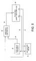
- FIG. 5shows an embodiment of the present invention wherein the reference frequency is generated in response to the clocking frequency.
- FIG. 6shows an embodiment of the present invention wherein the propagation delay circuit comprises a matched delay oscillator comprising matched delay circuitry substantially matched to the critical path circuit.
- FIG. 7shows an embodiment of the present invention wherein the propagation delay circuit comprises a plurality of matched delay circuits connected in series in order to scale the propagation delay frequency.
- FIG. 2shows a computing device according to an embodiment of the present invention comprising digital circuitry including a critical path circuit 26 , and a propagation delay circuit 28 for generating a propagation delay frequency 30 representing a propagation delay of the critical path circuit 26 .
- the computing devicefurther comprises a frequency generator 32 for generating a reference frequency 34 and a frequency comparator 36 for generating a frequency error signal 38 representing a difference between the reference frequency 34 and the propagation delay frequency 30 .
- An adjustable circuit 40responsive to the frequency error signal 38 , adjusts at least one of a supply voltage and a clocking frequency 42 applied to the critical path circuit 26 .
- Adjusting the supply voltage and/or clocking frequency in response to a frequency error signal representing the error in propagation delayovercomes many of the drawbacks associated with the prior art phase comparison techniques described above with reference to FIG. 1 .
- the frequency comparator 36generates the frequency error signal 38 in discrete-time (using, for example, digital circuitry) over multiple periods of the reference frequency thereby reducing the measurement error as compared to the prior art phase comparator 12 of FIG. 1 which generates a continuous-time PWM signal 14 for each period of the reference frequency.
- the tolerances in rise/fall times of the prior art phase comparator 12are not present with the frequency comparison technique shown in FIG. 2 .
- the frequency comparison technique of the present inventionprovides more flexibility, for example, if the critical path circuit changes relative to the mode of operation or if multiple critical paths are operating simultaneously.
- the frequency error signal 38is integrated 44 to generate an integrated frequency error signal 46 , wherein the adjustable circuit 40 is responsive to the integrated frequency error signal 46 . Adjusting the supply voltage and/or clocking frequency 42 in response to the integrated frequency error signal 46 forms a control loop which drives the frequency error signal 38 toward zero.
- the adjustable circuit 40is configured to output a high supply voltage and/or or low clocking frequency 42 when the computing device is initially turned on or when it switches between different critical path circuits corresponding to different operating modes. This allows the integrated frequency error signal 46 to settle to an acceptable value before enabling adaptive power consumption.
- FIG. 3Bshows another embodiment of the present invention comprising a scalar 45 for generating a proportional frequency error signal 47 which is added 49 to the integrated frequency error signal 46 to generate a proportional/integral frequency error signal 51 to thereby implement a proportional/integral (PI) control loop.
- the PI frequency error signal 51improves the transient response of the control loop as compared to the prior art phase comparison technique shown in FIG. 1 .
- the frequency error signal 38is integrated in discrete-time and the discrete-time signal 46 converted to a continuous-time signal applied to the adjustable circuit 40 .
- Thisovercomes the conversion tolerance of the prior art phase comparison technique described above with reference to FIG. 1 since the propagation delay error is driven to zero independent of any conversion errors associated with converting the discrete-time signal to a continuous-time signal applied to the adjustable circuit 40 . In other words, any conversion errors that would otherwise be present are integrated out.
- FIG. 4Ashows an embodiment of the present invention wherein the frequency comparator 36 comprises an up/down counter 48 .
- a multiplexer 50selects between the propagation delay frequency 30 and the reference frequency 34 as the clock signal 52 to the up/down counter 48 .
- a counter select circuit 54configures the multiplexer 50 to select the reference frequency 34 as the clock signal 52 and configures the up/down counter 48 to count up for a first interval.
- the counter select circuit 54then configures the multiplexer 50 to select the propagation delay frequency 30 as the clock signal 52 and configures the up/down counter 48 to count down for a second interval.
- the content of the up/down counter 48 after the up/down counting intervalsrepresents the difference in frequency between the propagation delay frequency 30 and the reference frequency 34 .
- a latch 55latches the digital output 56 of the up/down counter 48 , and the output 57 of the latch 55 is converted by conversion circuitry 58 into an analog signal 60 .
- the analog signal 60is filtered 62 , and the filtered signal 64 applied to the adjustable circuit 40 for adjusting the supply voltage and/or the clocking frequency 42 .
- the propagation delay frequency 30matches the reference frequency 34 when the supply voltage and/or clocking frequency 42 reaches a value corresponding to the target propagation delay for the critical path circuit 26 . That is, the output 56 of the up/down counter 48 will be zero after the up/down counting intervals if the adjustable circuit 40 is set to the target value. If the propagation delay frequency 30 falls below the reference frequency 34 , the up/down counter 48 will output 56 a positive value after the down counting interval thereby increasing the control signal 64 applied to the adjustable circuit 40 . Conversion errors in the conversion circuitry 58 cause a voltage/clock error in 42 , which is accounted for and substantially canceled by counter 48 .
- the up/down counter 48will underflow after the down counting interval and output 56 a negative value which will decrease the control signal 64 applied to the adjustable circuit 40 .
- the precision of this circuitis proportional to the length of the counter, allowing the precision of the measurement to be traded off against the response speed and freeing the design from dependence on the conversion method 58 and filter 62 .
- the target propagation delay frequency 30is substantially different than the reference frequency 34 .
- This embodimentincreases design flexibility, for example, if the critical path changes relative to the operating mode of the computing device or if two critical paths having significantly different propagation delays are operating simultaneously.
- the frequency comparator 36is configured appropriately to account for the offset between the target propagation delay frequency 30 and the reference frequency 34 .
- the up/down counter 48may be initialized with an offset value (positive or negative) at each reset to account for the offset between frequencies.
- the up counting intervalmay be different than the down counting interval to account for the offset between frequencies.
- the conversion circuitry 58comprises a digital-to-analog converter, and the up/down counter 48 is reset after each up/down counting cycle resulting in a proportional control loop.
- the output 56 of the up/down counter 48is integrated using a digital accumulator 66 which accumulates the output 56 of the up/down counter 48 at the end of each up/down counting interval.
- the digital accumulator 66outputs a digital value 68 that is converted into an analog signal 60 by conversion circuitry 58 , thereby implementing an integral control loop.
- integrating the propagation delay errorovercomes the conversion tolerance of the conversion circuitry 58 since the propagation delay error is driven to zero independent of any conversion errors associated with converting the discrete-time signal 68 to a continuous-time signal 60 applied to the adjustable circuit 40 .
- the integrating aspectis implemented by not resetting the up/down counter 48 at the end of each up/down counting cycle.
- FIG. 4Cshows an embodiment of the present invention wherein the up/down counter 48 is initialized with an offset value, and an OR gate 70 prevents the up/down counter from overflowing or underflowing. Also in this embodiment, the up/down counter 48 generates a PWM signal 72 from the most significant bit (MSBIT) of the counter value.
- the up/down counter 48is initialized with an offset value such that the duty cycle of the PWM signal 72 is 50% when the propagation delay error is zero. The duty cycle increases when the propagation delay error produces a lower propagation delay frequency 30 relative to the reference frequency 34 , and the duty cycle decreases when the propagation delay error produces a higher propagation delay frequency 30 relative to the reference frequency 34 .
- the digital PWM signal 72is converted into a suitable analog signal 60 by a conversion circuit 58 such as a suitable buffer circuit.
- FIG. 4Dshows an embodiment of the present invention wherein a first and second up/down counters 48 A and 48 B implement a proportional/integral control loop.
- the first up/down counter 48 Aoperates as described above with reference to FIG. 4A wherein the output 56 of the up/down counter 48 A is latched 69 and the up/down counter 48 A reset after the up/down counting interval.
- the output 71 of the latch 69is scaled by scalar 73 , and the resulting proportional frequency error signal 75 is applied to a first input of adder 77 .
- the second up/down counter 48 Boperates similar to the up/down counter described above with reference to FIG.
- the complete counter valueis output 79 continuously (at each clock cycle) to the second input of the adder 77 .
- the second up/down counter 48 Bis not reset at the end of the down counting interval such that the output 79 is an integrated frequency error signal.
- the most significant bit of the adder 77is output as a PWM signal 81 representing the proportional/integral frequency error signal applied to the conversion circuit 58 .
- the accuracy of the frequency error measurementis determined (or adjusted) by the length of the up/down counting intervals; however, increasing the up/down counting intervals increases the phase lag of the control loop.
- the scalar 73is adjusted to compensate for the increased phase lag and thereby achieve the desired frequency response.
- the frequency error signal 38is transmitted serially as a digital signal to the adjustable circuit 40 .
- the adjustable circuit 40is a conventional power driver integrated circuit that accepts other control signals over a serial input pin.
- FIG. 4EAn example of this embodiment is shown in FIG. 4E wherein a multiplexer 83 selects between the output 57 of the latch 55 and other control signals 85 as the input to a serial register 87 .
- the contents of the serial register 87are shifted out serially over line 89 and applied to a serial input pin of the adjustable circuit 40 .
- a control signal 91controls operation of the multiplexer 83 , serial register 87 , and adjustable circuit 40 in order to apply the appropriate control signals to the adjustable circuit 40 at the appropriate time.
- the frequency comparison technique of the present inventionfacilitates using a serial interface since the current frequency error signal can be transferred serially to the adjustable circuit 40 while computing the next frequency error signal (e.g., using the up/down counter 48 ). If the control loop comprises an integrator (e.g., by not resetting the up/down counter 48 ), the latch 55 may be omitted since any error in sampling the output 56 of the up/down counter 48 will be integrated out.
- the reference frequency 34is generated in response to the clocking frequency, and in an embodiment shown in FIG. 5 , the reference frequency 34 is the clocking frequency for clocking the digital circuitry including the critical path circuit 26 .
- This embodimentallows the clocking frequency to be adjusted, for example, to optimize power consumption or to change the operating frequency of the digital circuitry on-the-fly to facilitate different operating modes of the computing device.
- the target propagation delay of the critical path circuit 26scales inversely with a change in the clocking frequency (reference frequency 34 ). For example, if the clocking frequency (reference frequency 34 ) is decreased to reduce power consumption, the target propagation delay increases and the target propagation delay frequency 30 decreases proportionally.
- both the clocking frequency and the supply voltageare decreased.
- both the clocking frequency and the supply voltageare increased to meet the increased demand and the associated decrease in propagation delay of the critical path circuit 26 .
- the propagation delay circuit 28 of FIG. 2may be implemented using any suitable circuitry that generates a frequency representing the propagation delay of the critical path circuit 26 .
- the propagation delay circuit 28is implemented as a matched delay oscillator for generating the propagation delay frequency 30 .
- the matched delay oscillatorcomprises circuitry matching the critical path circuit 26 in both components and routing topology.
- the critical path circuit 26 and corresponding matched delay oscillatorcomprise a NAND gate 92 , a NOR gate 94 , an inverter 96 , an XOR gate 98 , and a multiplexer 100 .
- the output of the last component in the pathwraps around to the input of the first component in the path (the NAND gate 92 ) such that the propagation delay through the path results in an corresponding oscillation that is output as the propagation delay frequency 30 .
- the matched delay oscillatoralso comprises an enable buffer 102 for enabling/disabling the circuit, for example, relative to a mode of operation of the computing device.
- the propagation delay circuit 28does not exactly match the critical path circuit 26 but rather comprises circuitry and topology that emulates the critical path circuit 26 .
- the critical path circuit 26itself is configured into the propagation delay circuit 28 during a calibration mode. Once the optimal supply voltage and/or clocking frequency are determined during the calibration mode, the critical path circuit 26 is reconfigured for normal operation.
- FIG. 7shows yet another embodiment of the present invention wherein the propagation delay circuit 28 comprises a plurality of matched delay circuits 104 1 – 104 N connected in series in order to scale the propagation delay frequency 30 , wherein each matched delay circuit 104 i substantially matches the critical path circuit 26 .
- the propagation delay frequency 34decreases as more matched delay circuits 104 are added which may simplify certain implementation details, such as decreasing the reference frequency 34 or simplifying the frequency comparator 36 .
Landscapes
- Engineering & Computer Science (AREA)
- Theoretical Computer Science (AREA)
- Physics & Mathematics (AREA)
- General Engineering & Computer Science (AREA)
- General Physics & Mathematics (AREA)
- Stabilization Of Oscillater, Synchronisation, Frequency Synthesizers (AREA)
Abstract
Description
Claims (27)
Priority Applications (1)
| Application Number | Priority Date | Filing Date | Title |
|---|---|---|---|
| US10/983,382US7129763B1 (en) | 2004-11-08 | 2004-11-08 | Adjusting power consumption of digital circuitry by generating frequency error representing error in propagation delay |
Applications Claiming Priority (1)
| Application Number | Priority Date | Filing Date | Title |
|---|---|---|---|
| US10/983,382US7129763B1 (en) | 2004-11-08 | 2004-11-08 | Adjusting power consumption of digital circuitry by generating frequency error representing error in propagation delay |
Publications (1)
| Publication Number | Publication Date |
|---|---|
| US7129763B1true US7129763B1 (en) | 2006-10-31 |
Family
ID=37189223
Family Applications (1)
| Application Number | Title | Priority Date | Filing Date |
|---|---|---|---|
| US10/983,382Expired - LifetimeUS7129763B1 (en) | 2004-11-08 | 2004-11-08 | Adjusting power consumption of digital circuitry by generating frequency error representing error in propagation delay |
Country Status (1)
| Country | Link |
|---|---|
| US (1) | US7129763B1 (en) |
Cited By (152)
| Publication number | Priority date | Publication date | Assignee | Title |
|---|---|---|---|---|
| US20070096775A1 (en)* | 2005-10-31 | 2007-05-03 | Mohamed Elgebaly | Adaptive voltage scaling for an electronics device |
| US7330019B1 (en) | 2006-10-31 | 2008-02-12 | Western Digital Technologies, Inc. | Adjusting on-time for a discontinuous switching voltage regulator |
| US20080116964A1 (en)* | 2006-11-22 | 2008-05-22 | Kent Kernahan | Apparatus and method for controlling the propagation delay of a circuit by controlling the voltage applied to the circuit |
| US7486060B1 (en) | 2006-03-30 | 2009-02-03 | Western Digital Technologies, Inc. | Switching voltage regulator comprising a cycle comparator for dynamic voltage scaling |
| US7551383B1 (en)* | 2006-06-28 | 2009-06-23 | Western Digital Technologies, Inc. | Adjusting voltage delivered to disk drive circuitry based on a selected zone |
| US7733189B1 (en) | 2007-09-14 | 2010-06-08 | Western Digital Technologies, Inc. | Oscillator comprising foldover detection |
| WO2008079188A3 (en)* | 2006-11-22 | 2011-01-13 | Fyrestorm, Inc | Apparatus and method for controlling the propagation delay of a circuit by controlling the voltage applied to the circuit |
| WO2011085179A1 (en)* | 2010-01-08 | 2011-07-14 | Analog Devices, Inc. | Systems and methods for minimizing power consumption |
| US8085020B1 (en) | 2008-06-13 | 2011-12-27 | Western Digital Technologies, Inc. | Switching voltage regulator employing dynamic voltage scaling with hysteretic comparator |
| US8090902B1 (en) | 2009-05-22 | 2012-01-03 | Western Digital Technologies, Inc. | Disk drive adjusting command execution in response to control circuitry die temperature |
| US8324974B1 (en) | 2010-12-17 | 2012-12-04 | Western Digital Technologies, Inc. | Regulating power consumption of digital circuitry using a multi-layer ring oscillator |
| US8350628B1 (en) | 2011-02-15 | 2013-01-08 | Western Digital Technologies, Inc. | Gate speed regulator dithering ring oscillator to match critical path circuit |
| WO2013026040A1 (en)* | 2011-08-17 | 2013-02-21 | Broadcom Corporation | System for clocking an integrated circuit |
| US8390367B1 (en)* | 2011-02-15 | 2013-03-05 | Western Digital Technologies, Inc. | Ensuring minimum gate speed during startup of gate speed regulator |
| EP2239849A3 (en)* | 2009-04-06 | 2013-12-18 | Honeywell International Inc. | Apparatus and method for compensating for process, voltage, and temperature variation of the time delay of a digital delay line |
| WO2013174377A3 (en)* | 2012-05-23 | 2014-01-30 | Silicon Line Gmbh | Circuit arrangement and method for calibrating activation signals for voltage-controlled oscillators |
| US8879188B1 (en) | 2010-08-23 | 2014-11-04 | Western Digital Technologies, Inc. | Disk drive employing fly height calibration tracks to account for magnetic entropy and thermal decay |
| US8891193B1 (en) | 2013-05-09 | 2014-11-18 | Western Digital Technologies, Inc. | Disk drive calibrating threshold and gain of touchdown sensor |
| US8891341B1 (en) | 2013-03-11 | 2014-11-18 | Western Digital Technologies, Inc. | Energy assisted magnetic recording disk drive using modulated laser light |
| US8902529B1 (en) | 2012-11-20 | 2014-12-02 | Western Digital Technologies, Inc. | Dual frequency crystal oscillator |
| US8902527B1 (en) | 2010-03-22 | 2014-12-02 | Western Digital Technologies, Inc. | Systems and methods for improving sequential data rate performance using sorted data zones |
| US8909889B1 (en) | 2011-10-10 | 2014-12-09 | Western Digital Technologies, Inc. | Method and apparatus for servicing host commands by a disk drive |
| US8908311B1 (en) | 2014-01-27 | 2014-12-09 | Western Digital Technologies, Inc. | Data storage device writing a multi-sector codeword in segments over multiple disk revolutions |
| US8914625B1 (en) | 2009-07-31 | 2014-12-16 | Western Digital Technologies, Inc. | Automatically configuring a web browser file when booting an operating system from a data storage device |
| US8922939B1 (en) | 2013-04-02 | 2014-12-30 | Western Digital Technologies, Inc. | Disk drive generating feed-forward fly height control based on temperature sensitive fly height sensor |
| US8937404B1 (en) | 2010-08-23 | 2015-01-20 | Western Digital Technologies, Inc. | Data storage device comprising dual mode independent/parallel voltage regulators |
| US8937782B1 (en) | 2012-05-07 | 2015-01-20 | Western Digital Technologies, Inc. | Hard disk drive assembly including a NVSM to store configuration data for controlling disk drive operations |
| US20150022272A1 (en)* | 2013-07-22 | 2015-01-22 | Nvidia Corporation | Closed loop dynamic voltage and frequency scaling |
| US8941941B1 (en) | 2013-02-28 | 2015-01-27 | Western Digital Technologies, Inc. | Disk drive calibrating touchdown sensor |
| US8949521B1 (en) | 2013-04-10 | 2015-02-03 | Western Digital Technologies, Inc. | Actuator prepositioning for disk drive |
| US8947812B1 (en) | 2014-03-27 | 2015-02-03 | Western Digital Technologies, Inc. | Data storage device comprising equalizer filter and inter-track interference filter |
| US8953269B1 (en) | 2014-07-18 | 2015-02-10 | Western Digital Technologies, Inc. | Management of data objects in a data object zone |
| US8953277B1 (en) | 2014-06-16 | 2015-02-10 | Western Digital Technologies, Inc. | Data storage device writing tracks on a disk with equal spacing |
| US8954664B1 (en) | 2010-10-01 | 2015-02-10 | Western Digital Technologies, Inc. | Writing metadata files on a disk |
| US8958167B1 (en) | 2013-12-23 | 2015-02-17 | Western Digital Technologies, Inc. | Detection of disk surface irregularities in data storage devices |
| US8959281B1 (en) | 2012-11-09 | 2015-02-17 | Western Digital Technologies, Inc. | Data management for a storage device |
| US8970978B1 (en) | 2012-10-22 | 2015-03-03 | Western Digital Technologies, Inc. | Disk drive detecting head touchdown by applying DC+AC control signal to fly height actuator |
| US8976633B1 (en) | 2014-04-15 | 2015-03-10 | Western Digital Technologies, Inc. | Data storage device calibrating fly height actuator based on laser power for heat assisted magnetic recording |
| US8988809B1 (en) | 2014-02-18 | 2015-03-24 | Western Digital (Fremont), Llc | Disk recording device for writing a radially coherent reference band by measuring relative timing offsets of reference bursts |
| US8990493B1 (en) | 2011-06-30 | 2015-03-24 | Western Digital Technologies, Inc. | Method and apparatus for performing force unit access writes on a disk |
| US8988810B1 (en) | 2014-04-16 | 2015-03-24 | Western Digital Technologies, Inc. | Track measurement for data storage device |
| US8996839B1 (en) | 2012-01-23 | 2015-03-31 | Western Digital Technologies, Inc. | Data storage device aligning partition to boundary of sector when partition offset correlates with offset of write commands |
| US9001453B1 (en) | 2014-07-18 | 2015-04-07 | Western Digital Technologies, Inc. | Data storage device calibrating fly height actuator based on read mode touchdown resistance of touchdown sensor |
| US9009358B1 (en) | 2008-09-23 | 2015-04-14 | Western Digital Technologies, Inc. | Configuring a data storage device with a parameter file interlocked with configuration code |
| US9013818B1 (en) | 2013-12-06 | 2015-04-21 | Western Digital Technologies, Inc. | Disk drive measuring reader/writer gap by measuring fractional clock cycle over disk radius |
| US9013821B1 (en) | 2014-06-10 | 2015-04-21 | Western Digital Technologies, Inc. | Data storage device employing one-dimensional and two-dimensional channels |
| US9021410B1 (en) | 2013-12-10 | 2015-04-28 | Western Technologies, Inc. | Electronic system with multi-cycle simulation coverage mechanism and method of operation thereof |
| US9025267B1 (en) | 2014-06-09 | 2015-05-05 | Western Digital Technologies, Inc. | Data storage device using branch metric from adjacent track to compensate for inter-track interference |
| US9025421B1 (en) | 2014-10-08 | 2015-05-05 | Western Digital Technologies, Inc. | Data storage device adjusting laser input power to compensate for temperature variations |
| US9025270B1 (en) | 2013-09-17 | 2015-05-05 | Western Digital Technologies, Inc. | Electronic system with current conservation mechanism and method of operation thereof |
| US9047917B1 (en) | 2013-11-26 | 2015-06-02 | Western Digital Technologies, Inc. | Disk drive slider with sense amplifier for coupling to a preamp through a supply/bias line and a read signal line |
| US9049471B2 (en) | 2001-10-17 | 2015-06-02 | Keen Personal Media, Inc. | Personal video recorder for inserting a stored advertisement into a displayed broadcast stream |
| US9053730B1 (en) | 2012-05-11 | 2015-06-09 | Western Digital Technologies, Inc. | Disk drive comprising extended range head proximity sensor |
| US9053749B1 (en) | 2013-03-15 | 2015-06-09 | Western Digital Technologies, Inc. | Disk drive comprising a per-drive and per-head fly height filter |
| US9060420B2 (en) | 2007-11-01 | 2015-06-16 | Western Digitial Technologies, Inc. | Method of manufacturing a double sided flex circuit for a disk drive wherein a first side lead provides an etching mask for a second side lead |
| US9064542B1 (en) | 2013-04-08 | 2015-06-23 | Western Digital Technologies, Inc. | Scheduled load of heads to reduce lubricant migration on pole tip and decrease time to ready |
| US9064504B1 (en) | 2014-01-29 | 2015-06-23 | Western Digital Technologies, Inc. | Electronic system with media recovery mechanism and method of operation thereof |
| US9064525B2 (en) | 2013-11-26 | 2015-06-23 | Western Digital Technologies, Inc. | Disk drive comprising laser transmission line optimized for heat assisted magnetic recording |
| US9063838B1 (en) | 2012-01-23 | 2015-06-23 | Western Digital Technologies, Inc. | Data storage device shifting data chunks of alignment zone relative to sector boundaries |
| US20150180482A1 (en)* | 2013-12-23 | 2015-06-25 | Marvell Israel (M.I.S.L) Ltd. | Apparatus and method for reacting to a change in supply voltage |
| US9070406B1 (en) | 2014-03-10 | 2015-06-30 | Western Digital Technologies, Inc. | Disk drive configuring one-dimensional and two-dimensional recording areas based on read element spacing |
| US9076474B1 (en) | 2014-12-23 | 2015-07-07 | Western Digital Technologies, Inc. | Data storage device attenuating thermal decay effect on fly height measurement |
| US9074941B1 (en) | 2013-03-14 | 2015-07-07 | Western Digital Technologies, Inc. | Systems and methods for measuring ambient and laser temperature in heat assisted magnetic recording |
| US9075714B1 (en) | 2014-05-13 | 2015-07-07 | Western Digital Technologies, Inc. | Electronic system with data management mechanism and method of operation thereof |
| US9082458B1 (en) | 2014-03-10 | 2015-07-14 | Western Digital Technologies, Inc. | Data storage device balancing and maximizing quality metric when configuring arial density of each disk surface |
| US9099134B1 (en) | 2015-01-27 | 2015-08-04 | Western Digital Technologies, Inc. | Data storage device employing multiple jog profiles for a butterfly written disk surface |
| US9099103B1 (en) | 2014-10-21 | 2015-08-04 | Western Digital Technologies, Inc. | Heat assisted magnetic recording withinterlaced high-power heated and low-power heated tracks |
| US9099144B1 (en) | 2013-10-11 | 2015-08-04 | Western Digital Technologies, Inc. | Disk drive evaluating laser performance for heat assisted magnetic recording |
| US9117463B1 (en) | 2014-06-23 | 2015-08-25 | Western Digital Technologies, Inc. | Data storage device erasing multiple adjacent data tracks to recover from inter-track interference |
| US9117489B1 (en) | 2014-02-18 | 2015-08-25 | Western Digital Technologies, Inc. | Data storage device screening heads by verifying defects after defect scan |
| US9117479B1 (en) | 2014-09-24 | 2015-08-25 | Western Digital Technologies, Inc. | Data storage device calibrating laser write power for heat assisted magnetic recording |
| US9123382B1 (en) | 2014-10-28 | 2015-09-01 | Western Digital Technologies, Inc. | Non-volatile caching for sequence of data |
| US9123370B1 (en) | 2014-04-15 | 2015-09-01 | Western Digital Technologies, Inc. | Data storage device calibrating fly height actuator based on laser power for heat assisted magnetic recording |
| US9128820B1 (en) | 2012-06-18 | 2015-09-08 | Western Digital Technologies, Inc. | File management among different zones of storage media |
| US9129628B1 (en) | 2014-10-23 | 2015-09-08 | Western Digital Technologies, Inc. | Data management for data storage device with different track density regions |
| US9135205B1 (en) | 2013-05-01 | 2015-09-15 | Western Digital Technologies, Inc. | Data storage assembly for archive cold storage |
| US9134782B2 (en) | 2007-05-07 | 2015-09-15 | Nvidia Corporation | Maintaining optimum voltage supply to match performance of an integrated circuit |
| US9153266B1 (en) | 2014-09-11 | 2015-10-06 | Western Digital Technologies, Inc. | Data storage device measuring laser protrusion fly height profile |
| US9153287B1 (en) | 2013-05-13 | 2015-10-06 | Western Digital Technologies, Inc. | Data access for shingled magnetic recording media |
| US9158722B1 (en) | 2011-11-02 | 2015-10-13 | Western Digital Technologies, Inc. | Data storage device to communicate with a host in a SATA or a USB mode |
| US9164694B1 (en) | 2013-06-19 | 2015-10-20 | Western Digital Technologies, Inc. | Data storage device detecting read-before-write conditions and returning configurable return data |
| US9171575B1 (en) | 2014-06-23 | 2015-10-27 | Western Digital Technologies, Inc. | Data storage device detecting media defects by writing opposite polarity test pattern |
| US9183864B1 (en) | 2013-06-13 | 2015-11-10 | Western Digital Technologies, Inc. | Disk drive adjusting closed-loop fly height target based on change in open-loop fly height control signal |
| US9183877B1 (en) | 2015-03-20 | 2015-11-10 | Western Digital Technologies, Inc. | Data storage device comprising two-dimensional data dependent noise whitening filters for two-dimensional recording |
| US9189392B1 (en) | 2011-06-30 | 2015-11-17 | Western Digital Technologies, Inc. | Opportunistic defragmentation during garbage collection |
| US20150331433A1 (en)* | 2014-05-14 | 2015-11-19 | Advanced Micro Devices, Inc. | Hybrid system and method for determining performance levels based on thermal conditions within a processor |
| US9196302B1 (en) | 2015-03-18 | 2015-11-24 | Western Digital Technologies, Inc. | Electronic system with media maintenance mechanism and method of operation thereof |
| US9214186B1 (en) | 2015-03-23 | 2015-12-15 | Western Digital Technologies, Inc. | Data storage device measuring radial offset between read element and write element |
| US9213493B1 (en) | 2011-12-16 | 2015-12-15 | Western Digital Technologies, Inc. | Sorted serpentine mapping for storage drives |
| US9230605B1 (en) | 2014-12-01 | 2016-01-05 | Western Digital Technologies, Inc. | Data storage device maximizing areal density based on a target quality metric |
| US9230585B1 (en) | 2014-01-31 | 2016-01-05 | Western Digital Technologies, Inc. | Per wedge preheat DFH to improve data storage device performance |
| US9236086B1 (en) | 2014-10-15 | 2016-01-12 | Western Digital Technologies, Inc. | Methods for reducing operational latency of data storage systems |
| US9245558B1 (en) | 2014-05-09 | 2016-01-26 | Western Digital Technologies, Inc. | Electronic system with data management mechanism and method of operation thereof |
| US9245556B2 (en) | 2014-03-10 | 2016-01-26 | Western Digital Technologies, Inc. | Disk drive employing multiple read elements to increase radial band for two-dimensional magnetic recording |
| US9251844B1 (en) | 2014-06-02 | 2016-02-02 | Western Digital Technologies, Inc. | Waterfall method and apparatus for a data storage device read system |
| US9251856B1 (en) | 2014-05-30 | 2016-02-02 | Western Digial Technologies, Inc. | Read failover method and apparatus for a data storage system |
| US9257145B1 (en) | 2013-11-27 | 2016-02-09 | Western Digital Technologies, Inc. | Disk drive measuring down-track spacing of read sensors |
| US9257143B1 (en) | 2014-12-23 | 2016-02-09 | Western Digital Technologies, Inc. | Precautionary measures for data storage device environmental conditions |
| US9257146B1 (en) | 2014-02-11 | 2016-02-09 | Western Digital Technologies, Inc. | Data storage device comprising sequence detector compensating for inter-track interference |
| US9263088B2 (en) | 2014-03-21 | 2016-02-16 | Western Digital Technologies, Inc. | Data management for a data storage device using a last resort zone |
| US9268649B1 (en) | 2011-06-23 | 2016-02-23 | Western Digital Technologies, Inc. | Disk drive with recent write streams list for data refresh determination |
| US9268499B1 (en) | 2010-08-13 | 2016-02-23 | Western Digital Technologies, Inc. | Hybrid drive migrating high workload data from disk to non-volatile semiconductor memory |
| US9269393B1 (en) | 2014-12-08 | 2016-02-23 | Western Digital Technologies, Inc. | Electronic system with data refresh mechanism and method of operation thereof |
| US9281009B1 (en) | 2014-12-18 | 2016-03-08 | Western Digital Technologies, Inc. | Data storage device employing variable size interleave written track segments |
| US9311939B1 (en) | 2014-12-23 | 2016-04-12 | Western Digital Technologies, Inc. | Write-through media caching |
| US9318137B1 (en) | 2015-03-13 | 2016-04-19 | Western Digital Technologies, Inc. | Data storage device executing retry operation by buffering signal samples at different radial offsets |
| US9330715B1 (en) | 2010-03-22 | 2016-05-03 | Western Digital Technologies, Inc. | Mapping of shingled magnetic recording media |
| US9355666B1 (en) | 2013-09-30 | 2016-05-31 | Western Digital Technologies, Inc. | Disk drive measuring stroke difference between heads by detecting a difference between ramp contact |
| US9361938B1 (en) | 2015-04-16 | 2016-06-07 | Western Digital Technologies, Inc. | Disk defect management for a data storage device |
| US9368131B1 (en) | 2015-04-03 | 2016-06-14 | Western Digital (Fremont), Llc | Data storage device employing mirrored cross-track profiles for top and bottom disk surfaces |
| US9368132B1 (en) | 2015-09-04 | 2016-06-14 | Western Digital Technologies, Inc. | Data storage device employing differential write data signal and differential write pattern signal |
| US9383923B1 (en) | 2012-10-18 | 2016-07-05 | Western Digital Technologies, Inc. | Write pointer management for a disk drive |
| US9401165B1 (en) | 2014-05-05 | 2016-07-26 | Western Digital Technologies, Inc. | Method and system to monitor magnetic head loading and unloading stability for a data storage system |
| US9417628B2 (en) | 2013-03-13 | 2016-08-16 | Western Digital Technologies, Inc. | Production failure analysis system |
| US9424864B2 (en) | 2014-07-02 | 2016-08-23 | Western Digital Technologies, Inc. | Data management for a data storage device with zone relocation |
| US9437242B1 (en) | 2015-09-14 | 2016-09-06 | Western Digital Technologies, Inc. | Data storage device employing different frequency preambles in adjacent data tracks |
| US9466318B2 (en) | 2014-12-24 | 2016-10-11 | Western Digital Technologies, Inc. | Allowing fast data zone switches on data storage devices |
| US9466321B1 (en) | 2015-06-05 | 2016-10-11 | Western Digital Technologies, Inc. | Angular position tracking of data accesses to mitigate risk of data loss |
| US9472219B1 (en) | 2015-05-01 | 2016-10-18 | Western Digital Technologies, Inc. | Data storage device calibrating parameter for heat assisted magnetic recording |
| US9502068B1 (en) | 2015-04-08 | 2016-11-22 | Western Digital Technologies, Inc. | Data storage device updating laser power during non-write mode for heat assisted magnetic recording |
| US9501393B2 (en) | 2014-01-27 | 2016-11-22 | Western Digital Technologies, Inc. | Data storage system garbage collection based on at least one attribute |
| TWI560986B (en)* | 2011-11-02 | 2016-12-01 | Marvell World Trade Ltd | Integrated circuit |
| US9553537B1 (en)* | 2015-07-16 | 2017-01-24 | Actron Technology Corporation | De-glitch circuit and de-glitch method and short circuit protection device |
| US9588898B1 (en) | 2015-06-02 | 2017-03-07 | Western Digital Technologies, Inc. | Fullness control for media-based cache operating in a steady state |
| US9600205B1 (en) | 2014-09-22 | 2017-03-21 | Western Digital Technologies, Inc. | Power aware power safe write buffer |
| US9602083B2 (en) | 2013-07-03 | 2017-03-21 | Nvidia Corporation | Clock generation circuit that tracks critical path across process, voltage and temperature variation |
| US9632711B1 (en) | 2014-04-07 | 2017-04-25 | Western Digital Technologies, Inc. | Processing flush requests by utilizing storage system write notifications |
| US9639287B1 (en) | 2015-06-29 | 2017-05-02 | Western Digital Technologies, Inc. | Write command reporting |
| US9645752B1 (en) | 2014-04-07 | 2017-05-09 | Western Digital Technologies, Inc. | Identification of data committed to non-volatile memory by use of notification commands |
| US9652019B2 (en) | 2014-06-02 | 2017-05-16 | Advanced Micro Devices, Inc. | System and method for adjusting processor performance based on platform and ambient thermal conditions |
| US9672107B1 (en) | 2015-02-11 | 2017-06-06 | Western Digital Technologies, Inc. | Data protection for a data storage device |
| US9747928B1 (en) | 2014-09-25 | 2017-08-29 | Western Digital Technologies, Inc. | Data storage device modifying write operation when a laser mode hop is detected |
| US9761273B1 (en) | 2015-11-03 | 2017-09-12 | Western Digital Technologies, Inc. | Data storage device encoding and interleaving codewords to improve trellis sequence detection |
| US9842617B1 (en) | 2015-06-29 | 2017-12-12 | Western Digital Technologies, Inc. | Electronic system with head management mechanism and method of operation thereof |
| US9842622B1 (en) | 2014-12-23 | 2017-12-12 | Western Digital Technologies, Inc. | Data storage device having improved read failure tolerance |
| US9864529B1 (en) | 2014-01-27 | 2018-01-09 | Western Digital Technologies, Inc. | Host compatibility for host managed storage media |
| US9870281B1 (en) | 2015-03-20 | 2018-01-16 | Western Digital Technologies, Inc. | Power loss mitigation for data storage device |
| US9875055B1 (en) | 2014-08-04 | 2018-01-23 | Western Digital Technologies, Inc. | Check-pointing of metadata |
| US9916616B2 (en) | 2014-03-31 | 2018-03-13 | Western Digital Technologies, Inc. | Inventory management system using incremental capacity formats |
| US9933955B1 (en) | 2015-03-05 | 2018-04-03 | Western Digital Technologies, Inc. | Power safe write buffer for data storage device |
| US9939883B2 (en) | 2012-12-27 | 2018-04-10 | Nvidia Corporation | Supply-voltage control for device power management |
| US9952950B1 (en) | 2014-09-08 | 2018-04-24 | Western Digital Technologies, Inc. | Data management in RAID environment |
| US9959052B1 (en) | 2015-09-17 | 2018-05-01 | Western Digital Technologies, Inc. | Media based cache for data storage device |
| US10056920B1 (en) | 2015-11-03 | 2018-08-21 | Western Digital Technologies, Inc. | Data storage device encoding and interleaving codewords to improve trellis sequence detection |
| US10063257B1 (en) | 2015-11-03 | 2018-08-28 | Western Digital Technologies, Inc. | Data storage device encoding and interleaving codewords to improve trellis sequence detection |
| US10103719B2 (en) | 2013-07-22 | 2018-10-16 | Nvidia Corporation | Integrated voltage regulator with in-built process, temperature and aging compensation |
| US10282371B1 (en) | 2014-12-02 | 2019-05-07 | Western Digital Technologies, Inc. | Object storage device with probabilistic data structure |
| US10282096B1 (en) | 2014-12-17 | 2019-05-07 | Western Digital Technologies, Inc. | Identification of data with predetermined data pattern |
| US10365836B1 (en) | 2015-01-27 | 2019-07-30 | Western Digital Technologies, Inc. | Electronic system with declustered data protection by parity based on reliability and method of operation thereof |
| US10466763B2 (en) | 2013-12-02 | 2019-11-05 | Nvidia Corporation | Dynamic voltage-frequency scaling to limit power transients |
| US10469090B1 (en)* | 2017-02-23 | 2019-11-05 | Xilinx, Inc. | Inverter-based filter biasing with ring oscillator-based supply regulation |
| US10587253B1 (en) | 2018-11-29 | 2020-03-10 | Qualcomm Incorporated | Ring oscillator-based programmable delay line |
Citations (27)
| Publication number | Priority date | Publication date | Assignee | Title |
|---|---|---|---|---|
| US4675617A (en)* | 1986-02-03 | 1987-06-23 | Martin Kenneth W | Stable voltage controlled oscillator |
| US4737670A (en) | 1984-11-09 | 1988-04-12 | Lsi Logic Corporation | Delay control circuit |
| US4822144A (en)* | 1986-12-24 | 1989-04-18 | U.S. Philips Corporation | Electro-optic color display including luminescent layer and interference filter |
| US4922141A (en)* | 1986-10-07 | 1990-05-01 | Western Digital Corporation | Phase-locked loop delay line |
| US5146121A (en)* | 1991-10-24 | 1992-09-08 | Northern Telecom Limited | Signal delay apparatus employing a phase locked loop |
| US5440250A (en) | 1993-06-26 | 1995-08-08 | Deutsche Itt Industries Gmbh | Clock-generating circuit for clock-controlled logic circuits |
| US5440520A (en) | 1994-09-16 | 1995-08-08 | Intel Corporation | Integrated circuit device that selects its own supply voltage by controlling a power supply |
| US5638019A (en)* | 1995-11-17 | 1997-06-10 | International Business Machines Corporation | Accurately generating precisely skewed clock signals |
| US5777567A (en)* | 1996-06-14 | 1998-07-07 | Sun Microsystems, Inc. | System and method for serial to parallel data conversion using delay line |
| US6055287A (en)* | 1998-05-26 | 2000-04-25 | Mcewan; Thomas E. | Phase-comparator-less delay locked loop |
| US6125157A (en) | 1997-02-06 | 2000-09-26 | Rambus, Inc. | Delay-locked loop circuitry for clock delay adjustment |
| US6157247A (en) | 1996-08-07 | 2000-12-05 | Motorola, Inc. | Methods and circuits for dynamically adjusting a supply voltage and/or a frequency of a clock signal in a digital circuit |
| US6259293B1 (en)* | 1999-06-15 | 2001-07-10 | Mitsubishi Denki Kabushiki Kaisha | Delay circuitry, clock generating circuitry, and phase synchronization circuitry |
| US6333652B1 (en)* | 1999-05-27 | 2001-12-25 | Rohm Co. Ltd. | Delay circuit |
| US6356062B1 (en) | 2000-09-27 | 2002-03-12 | Intel Corporation | Degenerative load temperature correction for charge pumps |
| US6424184B1 (en) | 1996-09-25 | 2002-07-23 | Matsushita Electric Industrial Co., Ltd. | Frequency-voltage conversion circuit, delay amount judgement circuit, system having frequency-voltage conversion circuit, method of adjusting input/output characteristics of frequency-voltage conversion circuit, and apparatus for automatically adjusting input |
| US6425086B1 (en) | 1999-04-30 | 2002-07-23 | Intel Corporation | Method and apparatus for dynamic power control of a low power processor |
| US6449575B2 (en) | 1999-04-21 | 2002-09-10 | Hewlett-Packard Company | Voltage control of integrated circuits |
| US6525585B1 (en)* | 2000-11-21 | 2003-02-25 | Nec Corporation | Fixed-length delay generation circuit |
| US6535735B2 (en) | 2001-03-22 | 2003-03-18 | Skyworks Solutions, Inc. | Critical path adaptive power control |
| US20030093160A1 (en) | 2001-11-09 | 2003-05-15 | The Regents Of The University Of Colorado, A Body Corporate | Adaptive voltage regulator for powered digital devices |
| US6577535B2 (en) | 2001-02-16 | 2003-06-10 | Sandisk Corporation | Method and system for distributed power generation in multi-chip memory systems |
| US6617936B2 (en)* | 2001-02-20 | 2003-09-09 | Velio Communications, Inc. | Phase controlled oscillator |
| US6693473B2 (en) | 2002-03-19 | 2004-02-17 | Infineon Technologies Ag | Delay lock loop having a variable voltage regulator |
| US6868503B1 (en) | 2002-01-19 | 2005-03-15 | National Semiconductor Corporation | Adaptive voltage scaling digital processing component and method of operating the same |
| US6870410B1 (en) | 2002-10-15 | 2005-03-22 | National Semiconductor Corporation | All digital power supply system and method that provides a substantially constant supply voltage over changes in PVT without a band gap reference voltage |
| US20050218871A1 (en) | 2003-04-11 | 2005-10-06 | Inyup Kang | Dynamic voltage scaling for portable devices |
- 2004
- 2004-11-08USUS10/983,382patent/US7129763B1/ennot_activeExpired - Lifetime
Patent Citations (27)
| Publication number | Priority date | Publication date | Assignee | Title |
|---|---|---|---|---|
| US4737670A (en) | 1984-11-09 | 1988-04-12 | Lsi Logic Corporation | Delay control circuit |
| US4675617A (en)* | 1986-02-03 | 1987-06-23 | Martin Kenneth W | Stable voltage controlled oscillator |
| US4922141A (en)* | 1986-10-07 | 1990-05-01 | Western Digital Corporation | Phase-locked loop delay line |
| US4822144A (en)* | 1986-12-24 | 1989-04-18 | U.S. Philips Corporation | Electro-optic color display including luminescent layer and interference filter |
| US5146121A (en)* | 1991-10-24 | 1992-09-08 | Northern Telecom Limited | Signal delay apparatus employing a phase locked loop |
| US5440250A (en) | 1993-06-26 | 1995-08-08 | Deutsche Itt Industries Gmbh | Clock-generating circuit for clock-controlled logic circuits |
| US5440520A (en) | 1994-09-16 | 1995-08-08 | Intel Corporation | Integrated circuit device that selects its own supply voltage by controlling a power supply |
| US5638019A (en)* | 1995-11-17 | 1997-06-10 | International Business Machines Corporation | Accurately generating precisely skewed clock signals |
| US5777567A (en)* | 1996-06-14 | 1998-07-07 | Sun Microsystems, Inc. | System and method for serial to parallel data conversion using delay line |
| US6157247A (en) | 1996-08-07 | 2000-12-05 | Motorola, Inc. | Methods and circuits for dynamically adjusting a supply voltage and/or a frequency of a clock signal in a digital circuit |
| US6424184B1 (en) | 1996-09-25 | 2002-07-23 | Matsushita Electric Industrial Co., Ltd. | Frequency-voltage conversion circuit, delay amount judgement circuit, system having frequency-voltage conversion circuit, method of adjusting input/output characteristics of frequency-voltage conversion circuit, and apparatus for automatically adjusting input |
| US6125157A (en) | 1997-02-06 | 2000-09-26 | Rambus, Inc. | Delay-locked loop circuitry for clock delay adjustment |
| US6055287A (en)* | 1998-05-26 | 2000-04-25 | Mcewan; Thomas E. | Phase-comparator-less delay locked loop |
| US6449575B2 (en) | 1999-04-21 | 2002-09-10 | Hewlett-Packard Company | Voltage control of integrated circuits |
| US6425086B1 (en) | 1999-04-30 | 2002-07-23 | Intel Corporation | Method and apparatus for dynamic power control of a low power processor |
| US6333652B1 (en)* | 1999-05-27 | 2001-12-25 | Rohm Co. Ltd. | Delay circuit |
| US6259293B1 (en)* | 1999-06-15 | 2001-07-10 | Mitsubishi Denki Kabushiki Kaisha | Delay circuitry, clock generating circuitry, and phase synchronization circuitry |
| US6356062B1 (en) | 2000-09-27 | 2002-03-12 | Intel Corporation | Degenerative load temperature correction for charge pumps |
| US6525585B1 (en)* | 2000-11-21 | 2003-02-25 | Nec Corporation | Fixed-length delay generation circuit |
| US6577535B2 (en) | 2001-02-16 | 2003-06-10 | Sandisk Corporation | Method and system for distributed power generation in multi-chip memory systems |
| US6617936B2 (en)* | 2001-02-20 | 2003-09-09 | Velio Communications, Inc. | Phase controlled oscillator |
| US6535735B2 (en) | 2001-03-22 | 2003-03-18 | Skyworks Solutions, Inc. | Critical path adaptive power control |
| US20030093160A1 (en) | 2001-11-09 | 2003-05-15 | The Regents Of The University Of Colorado, A Body Corporate | Adaptive voltage regulator for powered digital devices |
| US6868503B1 (en) | 2002-01-19 | 2005-03-15 | National Semiconductor Corporation | Adaptive voltage scaling digital processing component and method of operating the same |
| US6693473B2 (en) | 2002-03-19 | 2004-02-17 | Infineon Technologies Ag | Delay lock loop having a variable voltage regulator |
| US6870410B1 (en) | 2002-10-15 | 2005-03-22 | National Semiconductor Corporation | All digital power supply system and method that provides a substantially constant supply voltage over changes in PVT without a band gap reference voltage |
| US20050218871A1 (en) | 2003-04-11 | 2005-10-06 | Inyup Kang | Dynamic voltage scaling for portable devices |
Non-Patent Citations (2)
| Title |
|---|
| G. Y. Wei, M. Horowitz, "A Fully Digital, Energy-Efficient, Adaptive Power-Supply Regulator" IEEE Journal of Solid State Circuits, vol. 34, No. 4, Apr. 1999. |
| T. D. Burd, T. A. Pering, R. W. Brodersen, "A Dynamic Voltage Scaled Microprocessor System" IEEE Journal of Solid State Circuits, vol. 35, No. 11, Nov. 2000. |
Cited By (177)
| Publication number | Priority date | Publication date | Assignee | Title |
|---|---|---|---|---|
| US9049471B2 (en) | 2001-10-17 | 2015-06-02 | Keen Personal Media, Inc. | Personal video recorder for inserting a stored advertisement into a displayed broadcast stream |
| US20070096775A1 (en)* | 2005-10-31 | 2007-05-03 | Mohamed Elgebaly | Adaptive voltage scaling for an electronics device |
| US7417482B2 (en)* | 2005-10-31 | 2008-08-26 | Qualcomm Incorporated | Adaptive voltage scaling for an electronics device |
| US7486060B1 (en) | 2006-03-30 | 2009-02-03 | Western Digital Technologies, Inc. | Switching voltage regulator comprising a cycle comparator for dynamic voltage scaling |
| US8912778B1 (en) | 2006-03-30 | 2014-12-16 | Western Digital Technologies, Inc. | Switching voltage regulator employing current pre-adjust based on power mode |
| US7551383B1 (en)* | 2006-06-28 | 2009-06-23 | Western Digital Technologies, Inc. | Adjusting voltage delivered to disk drive circuitry based on a selected zone |
| US7330019B1 (en) | 2006-10-31 | 2008-02-12 | Western Digital Technologies, Inc. | Adjusting on-time for a discontinuous switching voltage regulator |
| US20080116964A1 (en)* | 2006-11-22 | 2008-05-22 | Kent Kernahan | Apparatus and method for controlling the propagation delay of a circuit by controlling the voltage applied to the circuit |
| WO2008079188A3 (en)* | 2006-11-22 | 2011-01-13 | Fyrestorm, Inc | Apparatus and method for controlling the propagation delay of a circuit by controlling the voltage applied to the circuit |
| US9134782B2 (en) | 2007-05-07 | 2015-09-15 | Nvidia Corporation | Maintaining optimum voltage supply to match performance of an integrated circuit |
| US7733189B1 (en) | 2007-09-14 | 2010-06-08 | Western Digital Technologies, Inc. | Oscillator comprising foldover detection |
| US9060420B2 (en) | 2007-11-01 | 2015-06-16 | Western Digitial Technologies, Inc. | Method of manufacturing a double sided flex circuit for a disk drive wherein a first side lead provides an etching mask for a second side lead |
| US8085020B1 (en) | 2008-06-13 | 2011-12-27 | Western Digital Technologies, Inc. | Switching voltage regulator employing dynamic voltage scaling with hysteretic comparator |
| US9009358B1 (en) | 2008-09-23 | 2015-04-14 | Western Digital Technologies, Inc. | Configuring a data storage device with a parameter file interlocked with configuration code |
| EP2239849A3 (en)* | 2009-04-06 | 2013-12-18 | Honeywell International Inc. | Apparatus and method for compensating for process, voltage, and temperature variation of the time delay of a digital delay line |
| US8090902B1 (en) | 2009-05-22 | 2012-01-03 | Western Digital Technologies, Inc. | Disk drive adjusting command execution in response to control circuitry die temperature |
| US8914625B1 (en) | 2009-07-31 | 2014-12-16 | Western Digital Technologies, Inc. | Automatically configuring a web browser file when booting an operating system from a data storage device |
| US8258861B2 (en) | 2010-01-08 | 2012-09-04 | Analog Devices, Inc. | Systems and methods for minimizing power consumption |
| US20110169563A1 (en)* | 2010-01-08 | 2011-07-14 | Wreeju Bhaumik | Systems and methods for minimizing power consumption |
| WO2011085179A1 (en)* | 2010-01-08 | 2011-07-14 | Analog Devices, Inc. | Systems and methods for minimizing power consumption |
| US9330715B1 (en) | 2010-03-22 | 2016-05-03 | Western Digital Technologies, Inc. | Mapping of shingled magnetic recording media |
| US8902527B1 (en) | 2010-03-22 | 2014-12-02 | Western Digital Technologies, Inc. | Systems and methods for improving sequential data rate performance using sorted data zones |
| US9268499B1 (en) | 2010-08-13 | 2016-02-23 | Western Digital Technologies, Inc. | Hybrid drive migrating high workload data from disk to non-volatile semiconductor memory |
| US8879188B1 (en) | 2010-08-23 | 2014-11-04 | Western Digital Technologies, Inc. | Disk drive employing fly height calibration tracks to account for magnetic entropy and thermal decay |
| US8937404B1 (en) | 2010-08-23 | 2015-01-20 | Western Digital Technologies, Inc. | Data storage device comprising dual mode independent/parallel voltage regulators |
| US8954664B1 (en) | 2010-10-01 | 2015-02-10 | Western Digital Technologies, Inc. | Writing metadata files on a disk |
| US8324974B1 (en) | 2010-12-17 | 2012-12-04 | Western Digital Technologies, Inc. | Regulating power consumption of digital circuitry using a multi-layer ring oscillator |
| US8350628B1 (en) | 2011-02-15 | 2013-01-08 | Western Digital Technologies, Inc. | Gate speed regulator dithering ring oscillator to match critical path circuit |
| US8390367B1 (en)* | 2011-02-15 | 2013-03-05 | Western Digital Technologies, Inc. | Ensuring minimum gate speed during startup of gate speed regulator |
| US9268649B1 (en) | 2011-06-23 | 2016-02-23 | Western Digital Technologies, Inc. | Disk drive with recent write streams list for data refresh determination |
| US8990493B1 (en) | 2011-06-30 | 2015-03-24 | Western Digital Technologies, Inc. | Method and apparatus for performing force unit access writes on a disk |
| US9189392B1 (en) | 2011-06-30 | 2015-11-17 | Western Digital Technologies, Inc. | Opportunistic defragmentation during garbage collection |
| WO2013026032A1 (en)* | 2011-08-17 | 2013-02-21 | Broadcom Corporation | Adaptive clocking scheme to accommodate supply voltage transients |
| US10033391B2 (en) | 2011-08-17 | 2018-07-24 | Avago Technologies General Ip (Singapore) Pte. Ltd. | Adaptive clocking scheme |
| WO2013026040A1 (en)* | 2011-08-17 | 2013-02-21 | Broadcom Corporation | System for clocking an integrated circuit |
| US9312862B2 (en) | 2011-08-17 | 2016-04-12 | Broadcom Corporation | Adaptive clocking scheme to accommodate supply voltage transients |
| US10804906B2 (en) | 2011-08-17 | 2020-10-13 | Avago Technologies International Sales Pte. Limited | Adaptive clocking scheme |
| US9312863B2 (en) | 2011-08-17 | 2016-04-12 | Broadcom Corporation | Wave clocking |
| US8810300B2 (en) | 2011-08-17 | 2014-08-19 | Broadcom Corporation | Wave clocking |
| US8909889B1 (en) | 2011-10-10 | 2014-12-09 | Western Digital Technologies, Inc. | Method and apparatus for servicing host commands by a disk drive |
| TWI560986B (en)* | 2011-11-02 | 2016-12-01 | Marvell World Trade Ltd | Integrated circuit |
| US9158722B1 (en) | 2011-11-02 | 2015-10-13 | Western Digital Technologies, Inc. | Data storage device to communicate with a host in a SATA or a USB mode |
| US9213493B1 (en) | 2011-12-16 | 2015-12-15 | Western Digital Technologies, Inc. | Sorted serpentine mapping for storage drives |
| US8996839B1 (en) | 2012-01-23 | 2015-03-31 | Western Digital Technologies, Inc. | Data storage device aligning partition to boundary of sector when partition offset correlates with offset of write commands |
| US9063838B1 (en) | 2012-01-23 | 2015-06-23 | Western Digital Technologies, Inc. | Data storage device shifting data chunks of alignment zone relative to sector boundaries |
| US8937782B1 (en) | 2012-05-07 | 2015-01-20 | Western Digital Technologies, Inc. | Hard disk drive assembly including a NVSM to store configuration data for controlling disk drive operations |
| US9053730B1 (en) | 2012-05-11 | 2015-06-09 | Western Digital Technologies, Inc. | Disk drive comprising extended range head proximity sensor |
| WO2013174377A3 (en)* | 2012-05-23 | 2014-01-30 | Silicon Line Gmbh | Circuit arrangement and method for calibrating activation signals for voltage-controlled oscillators |
| US9484929B2 (en) | 2012-05-23 | 2016-11-01 | Silicon Line Gmbh | Circuit arrangement and method for calibrating activation signals for voltage-controlled oscillators |
| US9128820B1 (en) | 2012-06-18 | 2015-09-08 | Western Digital Technologies, Inc. | File management among different zones of storage media |
| US9477681B2 (en) | 2012-06-18 | 2016-10-25 | Western Digital Technologies, Inc. | File management among different zones of storage media |
| US9383923B1 (en) | 2012-10-18 | 2016-07-05 | Western Digital Technologies, Inc. | Write pointer management for a disk drive |
| US8970978B1 (en) | 2012-10-22 | 2015-03-03 | Western Digital Technologies, Inc. | Disk drive detecting head touchdown by applying DC+AC control signal to fly height actuator |
| US8959281B1 (en) | 2012-11-09 | 2015-02-17 | Western Digital Technologies, Inc. | Data management for a storage device |
| US8902529B1 (en) | 2012-11-20 | 2014-12-02 | Western Digital Technologies, Inc. | Dual frequency crystal oscillator |
| US10386916B2 (en) | 2012-12-27 | 2019-08-20 | Nvidia Corporation | Supply-voltage control for device power management |
| US9939883B2 (en) | 2012-12-27 | 2018-04-10 | Nvidia Corporation | Supply-voltage control for device power management |
| US8941941B1 (en) | 2013-02-28 | 2015-01-27 | Western Digital Technologies, Inc. | Disk drive calibrating touchdown sensor |
| US8891341B1 (en) | 2013-03-11 | 2014-11-18 | Western Digital Technologies, Inc. | Energy assisted magnetic recording disk drive using modulated laser light |
| US9417628B2 (en) | 2013-03-13 | 2016-08-16 | Western Digital Technologies, Inc. | Production failure analysis system |
| US9074941B1 (en) | 2013-03-14 | 2015-07-07 | Western Digital Technologies, Inc. | Systems and methods for measuring ambient and laser temperature in heat assisted magnetic recording |
| US9053749B1 (en) | 2013-03-15 | 2015-06-09 | Western Digital Technologies, Inc. | Disk drive comprising a per-drive and per-head fly height filter |
| US8922939B1 (en) | 2013-04-02 | 2014-12-30 | Western Digital Technologies, Inc. | Disk drive generating feed-forward fly height control based on temperature sensitive fly height sensor |
| US9064542B1 (en) | 2013-04-08 | 2015-06-23 | Western Digital Technologies, Inc. | Scheduled load of heads to reduce lubricant migration on pole tip and decrease time to ready |
| US8949521B1 (en) | 2013-04-10 | 2015-02-03 | Western Digital Technologies, Inc. | Actuator prepositioning for disk drive |
| US9135205B1 (en) | 2013-05-01 | 2015-09-15 | Western Digital Technologies, Inc. | Data storage assembly for archive cold storage |
| US8891193B1 (en) | 2013-05-09 | 2014-11-18 | Western Digital Technologies, Inc. | Disk drive calibrating threshold and gain of touchdown sensor |
| US9153287B1 (en) | 2013-05-13 | 2015-10-06 | Western Digital Technologies, Inc. | Data access for shingled magnetic recording media |
| US9183864B1 (en) | 2013-06-13 | 2015-11-10 | Western Digital Technologies, Inc. | Disk drive adjusting closed-loop fly height target based on change in open-loop fly height control signal |
| US9164694B1 (en) | 2013-06-19 | 2015-10-20 | Western Digital Technologies, Inc. | Data storage device detecting read-before-write conditions and returning configurable return data |
| US9912322B2 (en) | 2013-07-03 | 2018-03-06 | Nvidia Corporation | Clock generation circuit that tracks critical path across process, voltage and temperature variation |
| US9602083B2 (en) | 2013-07-03 | 2017-03-21 | Nvidia Corporation | Clock generation circuit that tracks critical path across process, voltage and temperature variation |
| US9766649B2 (en)* | 2013-07-22 | 2017-09-19 | Nvidia Corporation | Closed loop dynamic voltage and frequency scaling |
| US20150022272A1 (en)* | 2013-07-22 | 2015-01-22 | Nvidia Corporation | Closed loop dynamic voltage and frequency scaling |
| US10103719B2 (en) | 2013-07-22 | 2018-10-16 | Nvidia Corporation | Integrated voltage regulator with in-built process, temperature and aging compensation |
| US10200022B2 (en) | 2013-07-22 | 2019-02-05 | Nvidia Corporation | Integrated voltage regulator with in-built process, temperature and aging compensation |
| US9025270B1 (en) | 2013-09-17 | 2015-05-05 | Western Digital Technologies, Inc. | Electronic system with current conservation mechanism and method of operation thereof |
| US9355666B1 (en) | 2013-09-30 | 2016-05-31 | Western Digital Technologies, Inc. | Disk drive measuring stroke difference between heads by detecting a difference between ramp contact |
| US9099144B1 (en) | 2013-10-11 | 2015-08-04 | Western Digital Technologies, Inc. | Disk drive evaluating laser performance for heat assisted magnetic recording |
| US9064525B2 (en) | 2013-11-26 | 2015-06-23 | Western Digital Technologies, Inc. | Disk drive comprising laser transmission line optimized for heat assisted magnetic recording |
| US9047917B1 (en) | 2013-11-26 | 2015-06-02 | Western Digital Technologies, Inc. | Disk drive slider with sense amplifier for coupling to a preamp through a supply/bias line and a read signal line |
| US9299371B1 (en) | 2013-11-26 | 2016-03-29 | Western Digital Technologies, Inc. | Disk drive slider with sense amplifier for coupling to a preamp through a supply/bias line and a read signal line |
| US9257145B1 (en) | 2013-11-27 | 2016-02-09 | Western Digital Technologies, Inc. | Disk drive measuring down-track spacing of read sensors |
| US10466763B2 (en) | 2013-12-02 | 2019-11-05 | Nvidia Corporation | Dynamic voltage-frequency scaling to limit power transients |
| US9013818B1 (en) | 2013-12-06 | 2015-04-21 | Western Digital Technologies, Inc. | Disk drive measuring reader/writer gap by measuring fractional clock cycle over disk radius |
| US9021410B1 (en) | 2013-12-10 | 2015-04-28 | Western Technologies, Inc. | Electronic system with multi-cycle simulation coverage mechanism and method of operation thereof |
| US8958167B1 (en) | 2013-12-23 | 2015-02-17 | Western Digital Technologies, Inc. | Detection of disk surface irregularities in data storage devices |
| US20150180482A1 (en)* | 2013-12-23 | 2015-06-25 | Marvell Israel (M.I.S.L) Ltd. | Apparatus and method for reacting to a change in supply voltage |
| US9864529B1 (en) | 2014-01-27 | 2018-01-09 | Western Digital Technologies, Inc. | Host compatibility for host managed storage media |
| US8908311B1 (en) | 2014-01-27 | 2014-12-09 | Western Digital Technologies, Inc. | Data storage device writing a multi-sector codeword in segments over multiple disk revolutions |
| US9501393B2 (en) | 2014-01-27 | 2016-11-22 | Western Digital Technologies, Inc. | Data storage system garbage collection based on at least one attribute |
| US10282130B2 (en) | 2014-01-27 | 2019-05-07 | Western Digital Technologies, Inc. | Coherency of data in data relocation |
| US9064504B1 (en) | 2014-01-29 | 2015-06-23 | Western Digital Technologies, Inc. | Electronic system with media recovery mechanism and method of operation thereof |
| US9230585B1 (en) | 2014-01-31 | 2016-01-05 | Western Digital Technologies, Inc. | Per wedge preheat DFH to improve data storage device performance |
| US9257146B1 (en) | 2014-02-11 | 2016-02-09 | Western Digital Technologies, Inc. | Data storage device comprising sequence detector compensating for inter-track interference |
| US8988809B1 (en) | 2014-02-18 | 2015-03-24 | Western Digital (Fremont), Llc | Disk recording device for writing a radially coherent reference band by measuring relative timing offsets of reference bursts |
| US9117489B1 (en) | 2014-02-18 | 2015-08-25 | Western Digital Technologies, Inc. | Data storage device screening heads by verifying defects after defect scan |
| US9245556B2 (en) | 2014-03-10 | 2016-01-26 | Western Digital Technologies, Inc. | Disk drive employing multiple read elements to increase radial band for two-dimensional magnetic recording |
| US9070406B1 (en) | 2014-03-10 | 2015-06-30 | Western Digital Technologies, Inc. | Disk drive configuring one-dimensional and two-dimensional recording areas based on read element spacing |
| US9082458B1 (en) | 2014-03-10 | 2015-07-14 | Western Digital Technologies, Inc. | Data storage device balancing and maximizing quality metric when configuring arial density of each disk surface |
| US9263088B2 (en) | 2014-03-21 | 2016-02-16 | Western Digital Technologies, Inc. | Data management for a data storage device using a last resort zone |
| US8947812B1 (en) | 2014-03-27 | 2015-02-03 | Western Digital Technologies, Inc. | Data storage device comprising equalizer filter and inter-track interference filter |
| US9916616B2 (en) | 2014-03-31 | 2018-03-13 | Western Digital Technologies, Inc. | Inventory management system using incremental capacity formats |
| US9632711B1 (en) | 2014-04-07 | 2017-04-25 | Western Digital Technologies, Inc. | Processing flush requests by utilizing storage system write notifications |
| US10162534B1 (en) | 2014-04-07 | 2018-12-25 | Western Digital Technologies, Inc. | Ordering commitment of data from a data cache to nonvolatile memory using ordering commands |
| US9645752B1 (en) | 2014-04-07 | 2017-05-09 | Western Digital Technologies, Inc. | Identification of data committed to non-volatile memory by use of notification commands |
| US9123370B1 (en) | 2014-04-15 | 2015-09-01 | Western Digital Technologies, Inc. | Data storage device calibrating fly height actuator based on laser power for heat assisted magnetic recording |
| US8976633B1 (en) | 2014-04-15 | 2015-03-10 | Western Digital Technologies, Inc. | Data storage device calibrating fly height actuator based on laser power for heat assisted magnetic recording |
| US8988810B1 (en) | 2014-04-16 | 2015-03-24 | Western Digital Technologies, Inc. | Track measurement for data storage device |
| US9401165B1 (en) | 2014-05-05 | 2016-07-26 | Western Digital Technologies, Inc. | Method and system to monitor magnetic head loading and unloading stability for a data storage system |
| US9245558B1 (en) | 2014-05-09 | 2016-01-26 | Western Digital Technologies, Inc. | Electronic system with data management mechanism and method of operation thereof |
| US9075714B1 (en) | 2014-05-13 | 2015-07-07 | Western Digital Technologies, Inc. | Electronic system with data management mechanism and method of operation thereof |
| US20150331433A1 (en)* | 2014-05-14 | 2015-11-19 | Advanced Micro Devices, Inc. | Hybrid system and method for determining performance levels based on thermal conditions within a processor |
| US9671767B2 (en)* | 2014-05-14 | 2017-06-06 | Advanced Micro Devices, Inc. | Hybrid system and method for determining performance levels based on thermal conditions within a processor |
| US9251856B1 (en) | 2014-05-30 | 2016-02-02 | Western Digial Technologies, Inc. | Read failover method and apparatus for a data storage system |
| US9652019B2 (en) | 2014-06-02 | 2017-05-16 | Advanced Micro Devices, Inc. | System and method for adjusting processor performance based on platform and ambient thermal conditions |
| US9251844B1 (en) | 2014-06-02 | 2016-02-02 | Western Digital Technologies, Inc. | Waterfall method and apparatus for a data storage device read system |
| US9025267B1 (en) | 2014-06-09 | 2015-05-05 | Western Digital Technologies, Inc. | Data storage device using branch metric from adjacent track to compensate for inter-track interference |
| US9013821B1 (en) | 2014-06-10 | 2015-04-21 | Western Digital Technologies, Inc. | Data storage device employing one-dimensional and two-dimensional channels |
| US8953277B1 (en) | 2014-06-16 | 2015-02-10 | Western Digital Technologies, Inc. | Data storage device writing tracks on a disk with equal spacing |
| US9171575B1 (en) | 2014-06-23 | 2015-10-27 | Western Digital Technologies, Inc. | Data storage device detecting media defects by writing opposite polarity test pattern |
| US9117463B1 (en) | 2014-06-23 | 2015-08-25 | Western Digital Technologies, Inc. | Data storage device erasing multiple adjacent data tracks to recover from inter-track interference |
| US9424864B2 (en) | 2014-07-02 | 2016-08-23 | Western Digital Technologies, Inc. | Data management for a data storage device with zone relocation |
| US9001453B1 (en) | 2014-07-18 | 2015-04-07 | Western Digital Technologies, Inc. | Data storage device calibrating fly height actuator based on read mode touchdown resistance of touchdown sensor |
| US8953269B1 (en) | 2014-07-18 | 2015-02-10 | Western Digital Technologies, Inc. | Management of data objects in a data object zone |
| US9875055B1 (en) | 2014-08-04 | 2018-01-23 | Western Digital Technologies, Inc. | Check-pointing of metadata |
| US9952950B1 (en) | 2014-09-08 | 2018-04-24 | Western Digital Technologies, Inc. | Data management in RAID environment |
| US10572358B1 (en) | 2014-09-08 | 2020-02-25 | Western Digital Technologies, Inc. | Data management in RAID environment |
| US9153266B1 (en) | 2014-09-11 | 2015-10-06 | Western Digital Technologies, Inc. | Data storage device measuring laser protrusion fly height profile |
| US9600205B1 (en) | 2014-09-22 | 2017-03-21 | Western Digital Technologies, Inc. | Power aware power safe write buffer |
| US9117479B1 (en) | 2014-09-24 | 2015-08-25 | Western Digital Technologies, Inc. | Data storage device calibrating laser write power for heat assisted magnetic recording |
| US9972344B2 (en) | 2014-09-25 | 2018-05-15 | Western Digital Technologies, Inc. | Data storage device modifying write operation when a laser mode hop is detected |
| US9747928B1 (en) | 2014-09-25 | 2017-08-29 | Western Digital Technologies, Inc. | Data storage device modifying write operation when a laser mode hop is detected |
| US9025421B1 (en) | 2014-10-08 | 2015-05-05 | Western Digital Technologies, Inc. | Data storage device adjusting laser input power to compensate for temperature variations |
| US9236086B1 (en) | 2014-10-15 | 2016-01-12 | Western Digital Technologies, Inc. | Methods for reducing operational latency of data storage systems |
| US9099103B1 (en) | 2014-10-21 | 2015-08-04 | Western Digital Technologies, Inc. | Heat assisted magnetic recording withinterlaced high-power heated and low-power heated tracks |
| US9129628B1 (en) | 2014-10-23 | 2015-09-08 | Western Digital Technologies, Inc. | Data management for data storage device with different track density regions |
| US9123382B1 (en) | 2014-10-28 | 2015-09-01 | Western Digital Technologies, Inc. | Non-volatile caching for sequence of data |
| US9230605B1 (en) | 2014-12-01 | 2016-01-05 | Western Digital Technologies, Inc. | Data storage device maximizing areal density based on a target quality metric |
| US10282371B1 (en) | 2014-12-02 | 2019-05-07 | Western Digital Technologies, Inc. | Object storage device with probabilistic data structure |
| US9269393B1 (en) | 2014-12-08 | 2016-02-23 | Western Digital Technologies, Inc. | Electronic system with data refresh mechanism and method of operation thereof |
| US10282096B1 (en) | 2014-12-17 | 2019-05-07 | Western Digital Technologies, Inc. | Identification of data with predetermined data pattern |
| US9281009B1 (en) | 2014-12-18 | 2016-03-08 | Western Digital Technologies, Inc. | Data storage device employing variable size interleave written track segments |
| US9257143B1 (en) | 2014-12-23 | 2016-02-09 | Western Digital Technologies, Inc. | Precautionary measures for data storage device environmental conditions |
| US9311939B1 (en) | 2014-12-23 | 2016-04-12 | Western Digital Technologies, Inc. | Write-through media caching |
| US9076474B1 (en) | 2014-12-23 | 2015-07-07 | Western Digital Technologies, Inc. | Data storage device attenuating thermal decay effect on fly height measurement |
| US9842622B1 (en) | 2014-12-23 | 2017-12-12 | Western Digital Technologies, Inc. | Data storage device having improved read failure tolerance |
| US9466318B2 (en) | 2014-12-24 | 2016-10-11 | Western Digital Technologies, Inc. | Allowing fast data zone switches on data storage devices |
| US9099134B1 (en) | 2015-01-27 | 2015-08-04 | Western Digital Technologies, Inc. | Data storage device employing multiple jog profiles for a butterfly written disk surface |
| US10365836B1 (en) | 2015-01-27 | 2019-07-30 | Western Digital Technologies, Inc. | Electronic system with declustered data protection by parity based on reliability and method of operation thereof |
| US9672107B1 (en) | 2015-02-11 | 2017-06-06 | Western Digital Technologies, Inc. | Data protection for a data storage device |
| US9933955B1 (en) | 2015-03-05 | 2018-04-03 | Western Digital Technologies, Inc. | Power safe write buffer for data storage device |
| US9318137B1 (en) | 2015-03-13 | 2016-04-19 | Western Digital Technologies, Inc. | Data storage device executing retry operation by buffering signal samples at different radial offsets |
| US9196302B1 (en) | 2015-03-18 | 2015-11-24 | Western Digital Technologies, Inc. | Electronic system with media maintenance mechanism and method of operation thereof |
| US9183877B1 (en) | 2015-03-20 | 2015-11-10 | Western Digital Technologies, Inc. | Data storage device comprising two-dimensional data dependent noise whitening filters for two-dimensional recording |
| US9870281B1 (en) | 2015-03-20 | 2018-01-16 | Western Digital Technologies, Inc. | Power loss mitigation for data storage device |
| US9214186B1 (en) | 2015-03-23 | 2015-12-15 | Western Digital Technologies, Inc. | Data storage device measuring radial offset between read element and write element |
| US9384774B1 (en) | 2015-03-23 | 2016-07-05 | Western Digital Technologies, Inc. | Data storage device calibrating a laser power for heat assisted magnetic recording based on slope of quality metric |
| US9368131B1 (en) | 2015-04-03 | 2016-06-14 | Western Digital (Fremont), Llc | Data storage device employing mirrored cross-track profiles for top and bottom disk surfaces |
| US9502068B1 (en) | 2015-04-08 | 2016-11-22 | Western Digital Technologies, Inc. | Data storage device updating laser power during non-write mode for heat assisted magnetic recording |
| US9361938B1 (en) | 2015-04-16 | 2016-06-07 | Western Digital Technologies, Inc. | Disk defect management for a data storage device |
| US9472219B1 (en) | 2015-05-01 | 2016-10-18 | Western Digital Technologies, Inc. | Data storage device calibrating parameter for heat assisted magnetic recording |
| US9588898B1 (en) | 2015-06-02 | 2017-03-07 | Western Digital Technologies, Inc. | Fullness control for media-based cache operating in a steady state |
| US9466321B1 (en) | 2015-06-05 | 2016-10-11 | Western Digital Technologies, Inc. | Angular position tracking of data accesses to mitigate risk of data loss |
| US9842617B1 (en) | 2015-06-29 | 2017-12-12 | Western Digital Technologies, Inc. | Electronic system with head management mechanism and method of operation thereof |
| US9639287B1 (en) | 2015-06-29 | 2017-05-02 | Western Digital Technologies, Inc. | Write command reporting |
| US9553537B1 (en)* | 2015-07-16 | 2017-01-24 | Actron Technology Corporation | De-glitch circuit and de-glitch method and short circuit protection device |
| US9368132B1 (en) | 2015-09-04 | 2016-06-14 | Western Digital Technologies, Inc. | Data storage device employing differential write data signal and differential write pattern signal |
| US9437242B1 (en) | 2015-09-14 | 2016-09-06 | Western Digital Technologies, Inc. | Data storage device employing different frequency preambles in adjacent data tracks |
| US9959052B1 (en) | 2015-09-17 | 2018-05-01 | Western Digital Technologies, Inc. | Media based cache for data storage device |
| US9761273B1 (en) | 2015-11-03 | 2017-09-12 | Western Digital Technologies, Inc. | Data storage device encoding and interleaving codewords to improve trellis sequence detection |
| US10063257B1 (en) | 2015-11-03 | 2018-08-28 | Western Digital Technologies, Inc. | Data storage device encoding and interleaving codewords to improve trellis sequence detection |
| US10554225B2 (en) | 2015-11-03 | 2020-02-04 | Western Digital Technologies, Inc. | Data storage device encoding and interleaving codewords to improve trellis sequence detection |
| US10554221B2 (en) | 2015-11-03 | 2020-02-04 | Western Digital Technologies, Inc. | Data storage device encoding and interleaving codewords to improve trellis sequence detection |
| US10056920B1 (en) | 2015-11-03 | 2018-08-21 | Western Digital Technologies, Inc. | Data storage device encoding and interleaving codewords to improve trellis sequence detection |
| US10469090B1 (en)* | 2017-02-23 | 2019-11-05 | Xilinx, Inc. | Inverter-based filter biasing with ring oscillator-based supply regulation |
| US10587253B1 (en) | 2018-11-29 | 2020-03-10 | Qualcomm Incorporated | Ring oscillator-based programmable delay line |
Similar Documents
| Publication | Publication Date | Title |
|---|---|---|
| US7129763B1 (en) | Adjusting power consumption of digital circuitry by generating frequency error representing error in propagation delay | |
| US7205805B1 (en) | Adjusting power consumption of digital circuitry relative to critical path circuit having the largest propagation delay error | |
| US7667625B2 (en) | Universal and fault-tolerant multiphase digital PWM controller for high-frequency DC-DC converters | |
| US7106040B1 (en) | Adaptive voltage scaling power supply for use in a digital processing component and method of operating the same | |
| US7459951B2 (en) | Self-calibrating digital pulse-width modulator (DPWM) | |
| US7117378B1 (en) | Adaptive voltage scaling digital processing component and method of operating the same | |
| US8912778B1 (en) | Switching voltage regulator employing current pre-adjust based on power mode | |
| JP5864507B2 (en) | Techniques for generating non-overlapping clocks | |
| JP4825291B2 (en) | Adaptive voltage scaling clock generator for use in digital processing components and method of operation thereof | |
| CN102025276B (en) | Clock domain crossing controller of digital control switch power supply and control method thereof | |
| US8044690B2 (en) | System and method for clock-synchronized triangular waveform generation | |
| CN105743463A (en) | Clock duty cycle correction and frequency multiplication circuit | |
| US8723571B2 (en) | Digital frequency locked loop | |
| WO1998013742A1 (en) | Frequency-voltage conversion circuit, delay amount judgement circuit, system having frequency-voltage conversion circuit, method of adjusting input/output characterictics of frequency-voltage conversion circuit, and apparatus for automatically adjusting input/output characteristics of frequency-voltage conversion circuit | |
| US20230114027A1 (en) | Method and Apparatus for Controlling Clock Cycle Time | |
| US6985025B1 (en) | System for adjusting a power supply level of a digital processing component and method of operating the same | |
| CN114710154A (en) | Open-loop fractional frequency divider and clock system based on time division multiplexing gain calibration | |
| CN111884631A (en) | A Digital Pulse Width Modulation Module Using Hybrid Structure | |
| US20110121880A1 (en) | Dc offset cancellation circuit | |
| KR102644945B1 (en) | Method and device to supply clock frequency | |
| US7834794B2 (en) | A/D converter | |
| CN108304019B (en) | voltage regulator | |
| EP3675361A1 (en) | Phase difference generator error compensation method of digital frequency generator | |
| CN116155205A (en) | Frequency doubling circuit | |
| US20080007313A1 (en) | Digital clock generator |
Legal Events
| Date | Code | Title | Description |
|---|---|---|---|
| AS | Assignment | Owner name:WESTERN DIGITAL TECHNOLOGIES, INC., CALIFORNIA Free format text:ASSIGNMENT OF ASSIGNORS INTEREST;ASSIGNORS:BENNETT, GEORGE J.;VASQUEZ, STEVEN R.;REEL/FRAME:015978/0105;SIGNING DATES FROM 20041004 TO 20041007 | |
| STCF | Information on status: patent grant | Free format text:PATENTED CASE | |
| FPAY | Fee payment | Year of fee payment:4 | |
| FPAY | Fee payment | Year of fee payment:8 | |
| AS | Assignment | Owner name:JPMORGAN CHASE BANK, N.A., AS COLLATERAL AGENT, ILLINOIS Free format text:SECURITY AGREEMENT;ASSIGNOR:WESTERN DIGITAL TECHNOLOGIES, INC.;REEL/FRAME:038722/0229 Effective date:20160512 Owner name:JPMORGAN CHASE BANK, N.A., AS COLLATERAL AGENT, ILLINOIS Free format text:SECURITY AGREEMENT;ASSIGNOR:WESTERN DIGITAL TECHNOLOGIES, INC.;REEL/FRAME:038744/0481 Effective date:20160512 Owner name:U.S. BANK NATIONAL ASSOCIATION, AS COLLATERAL AGENT, CALIFORNIA Free format text:SECURITY AGREEMENT;ASSIGNOR:WESTERN DIGITAL TECHNOLOGIES, INC.;REEL/FRAME:038744/0281 Effective date:20160512 Owner name:JPMORGAN CHASE BANK, N.A., AS COLLATERAL AGENT, IL Free format text:SECURITY AGREEMENT;ASSIGNOR:WESTERN DIGITAL TECHNOLOGIES, INC.;REEL/FRAME:038722/0229 Effective date:20160512 Owner name:JPMORGAN CHASE BANK, N.A., AS COLLATERAL AGENT, IL Free format text:SECURITY AGREEMENT;ASSIGNOR:WESTERN DIGITAL TECHNOLOGIES, INC.;REEL/FRAME:038744/0481 Effective date:20160512 Owner name:U.S. BANK NATIONAL ASSOCIATION, AS COLLATERAL AGEN Free format text:SECURITY AGREEMENT;ASSIGNOR:WESTERN DIGITAL TECHNOLOGIES, INC.;REEL/FRAME:038744/0281 Effective date:20160512 | |
| AS | Assignment | Owner name:WESTERN DIGITAL TECHNOLOGIES, INC., CALIFORNIA Free format text:RELEASE BY SECURED PARTY;ASSIGNOR:U.S. BANK NATIONAL ASSOCIATION, AS COLLATERAL AGENT;REEL/FRAME:045501/0714 Effective date:20180227 | |
| MAFP | Maintenance fee payment | Free format text:PAYMENT OF MAINTENANCE FEE, 12TH YEAR, LARGE ENTITY (ORIGINAL EVENT CODE: M1553) Year of fee payment:12 | |
| AS | Assignment | Owner name:WESTERN DIGITAL TECHNOLOGIES, INC., CALIFORNIA Free format text:RELEASE OF SECURITY INTEREST AT REEL 038744 FRAME 0481;ASSIGNOR:JPMORGAN CHASE BANK, N.A.;REEL/FRAME:058982/0556 Effective date:20220203 | |
| AS | Assignment | Owner name:JPMORGAN CHASE BANK, N.A., ILLINOIS Free format text:PATENT COLLATERAL AGREEMENT - A&R LOAN AGREEMENT;ASSIGNOR:WESTERN DIGITAL TECHNOLOGIES, INC.;REEL/FRAME:064715/0001 Effective date:20230818 Owner name:JPMORGAN CHASE BANK, N.A., ILLINOIS Free format text:PATENT COLLATERAL AGREEMENT - DDTL LOAN AGREEMENT;ASSIGNOR:WESTERN DIGITAL TECHNOLOGIES, INC.;REEL/FRAME:067045/0156 Effective date:20230818 |