US7129108B2 - CMOS image sensor and manufacturing method thereof - Google Patents
CMOS image sensor and manufacturing method thereofDownload PDFInfo
- Publication number
- US7129108B2 US7129108B2US10/956,202US95620204AUS7129108B2US 7129108 B2US7129108 B2US 7129108B2US 95620204 AUS95620204 AUS 95620204AUS 7129108 B2US7129108 B2US 7129108B2
- Authority
- US
- United States
- Prior art keywords
- color filter
- layer
- forming
- isolation
- isolation layer
- Prior art date
- Legal status (The legal status is an assumption and is not a legal conclusion. Google has not performed a legal analysis and makes no representation as to the accuracy of the status listed.)
- Expired - Fee Related
Links
- 238000004519manufacturing processMethods0.000titleclaimsdescription14
- 239000010410layerSubstances0.000claimsabstractdescription150
- 238000002955isolationMethods0.000claimsabstractdescription82
- 229910052751metalInorganic materials0.000claimsabstractdescription31
- 239000002184metalSubstances0.000claimsabstractdescription31
- 239000000758substrateSubstances0.000claimsabstractdescription22
- 239000011229interlayerSubstances0.000claimsabstractdescription17
- 238000000034methodMethods0.000claimsdescription49
- 229910052814silicon oxideInorganic materials0.000claimsdescription16
- 239000004065semiconductorSubstances0.000claimsdescription12
- VYPSYNLAJGMNEJ-UHFFFAOYSA-NSilicium dioxideChemical compoundO=[Si]=OVYPSYNLAJGMNEJ-UHFFFAOYSA-N0.000claimsdescription9
- 229910052581Si3N4Inorganic materials0.000claimsdescription7
- BOTDANWDWHJENH-UHFFFAOYSA-NTetraethyl orthosilicateChemical compoundCCO[Si](OCC)(OCC)OCCBOTDANWDWHJENH-UHFFFAOYSA-N0.000claimsdescription7
- HQVNEWCFYHHQES-UHFFFAOYSA-Nsilicon nitrideChemical compoundN12[Si]34N5[Si]62N3[Si]51N64HQVNEWCFYHHQES-UHFFFAOYSA-N0.000claimsdescription7
- -1silicon oxide nitrideChemical class0.000claimsdescription7
- 238000005229chemical vapour depositionMethods0.000claimsdescription6
- 238000004528spin coatingMethods0.000claimsdescription6
- 229920002120photoresistant polymerPolymers0.000description19
- 230000015572biosynthetic processEffects0.000description9
- 238000000151depositionMethods0.000description8
- 239000003086colorantSubstances0.000description4
- 230000008021depositionEffects0.000description3
- 238000004380ashingMethods0.000description2
- 239000003990capacitorSubstances0.000description2
- 150000002500ionsChemical class0.000description2
- 229910021420polycrystalline siliconInorganic materials0.000description2
- 229920005591polysiliconPolymers0.000description2
- 238000012545processingMethods0.000description2
- WQJQOUPTWCFRMM-UHFFFAOYSA-Ntungsten disilicideChemical compound[Si]#[W]#[Si]WQJQOUPTWCFRMM-UHFFFAOYSA-N0.000description2
- 229910021342tungsten silicideInorganic materials0.000description2
- 230000015556catabolic processEffects0.000description1
- 230000000295complement effectEffects0.000description1
- 238000007796conventional methodMethods0.000description1
- 230000007547defectEffects0.000description1
- 238000006731degradation reactionMethods0.000description1
- 230000003628erosive effectEffects0.000description1
- 238000005530etchingMethods0.000description1
- 239000007943implantSubstances0.000description1
- 239000012535impuritySubstances0.000description1
- 238000005468ion implantationMethods0.000description1
- 229910044991metal oxideInorganic materials0.000description1
- 150000004706metal oxidesChemical class0.000description1
- 238000012986modificationMethods0.000description1
- 230000004048modificationEffects0.000description1
- 230000003287optical effectEffects0.000description1
- 230000002093peripheral effectEffects0.000description1
- 239000000523sampleSubstances0.000description1
- 238000012360testing methodMethods0.000description1
Images


Classifications
- H—ELECTRICITY
- H10—SEMICONDUCTOR DEVICES; ELECTRIC SOLID-STATE DEVICES NOT OTHERWISE PROVIDED FOR
- H10F—INORGANIC SEMICONDUCTOR DEVICES SENSITIVE TO INFRARED RADIATION, LIGHT, ELECTROMAGNETIC RADIATION OF SHORTER WAVELENGTH OR CORPUSCULAR RADIATION
- H10F39/00—Integrated devices, or assemblies of multiple devices, comprising at least one element covered by group H10F30/00, e.g. radiation detectors comprising photodiode arrays
- H10F39/10—Integrated devices
- H10F39/12—Image sensors
- H—ELECTRICITY
- H10—SEMICONDUCTOR DEVICES; ELECTRIC SOLID-STATE DEVICES NOT OTHERWISE PROVIDED FOR
- H10F—INORGANIC SEMICONDUCTOR DEVICES SENSITIVE TO INFRARED RADIATION, LIGHT, ELECTROMAGNETIC RADIATION OF SHORTER WAVELENGTH OR CORPUSCULAR RADIATION
- H10F39/00—Integrated devices, or assemblies of multiple devices, comprising at least one element covered by group H10F30/00, e.g. radiation detectors comprising photodiode arrays
- H10F39/80—Constructional details of image sensors
- H10F39/811—Interconnections
- H—ELECTRICITY
- H10—SEMICONDUCTOR DEVICES; ELECTRIC SOLID-STATE DEVICES NOT OTHERWISE PROVIDED FOR
- H10F—INORGANIC SEMICONDUCTOR DEVICES SENSITIVE TO INFRARED RADIATION, LIGHT, ELECTROMAGNETIC RADIATION OF SHORTER WAVELENGTH OR CORPUSCULAR RADIATION
- H10F39/00—Integrated devices, or assemblies of multiple devices, comprising at least one element covered by group H10F30/00, e.g. radiation detectors comprising photodiode arrays
- H10F39/011—Manufacture or treatment of image sensors covered by group H10F39/12
- H10F39/024—Manufacture or treatment of image sensors covered by group H10F39/12 of coatings or optical elements
- H—ELECTRICITY
- H10—SEMICONDUCTOR DEVICES; ELECTRIC SOLID-STATE DEVICES NOT OTHERWISE PROVIDED FOR
- H10F—INORGANIC SEMICONDUCTOR DEVICES SENSITIVE TO INFRARED RADIATION, LIGHT, ELECTROMAGNETIC RADIATION OF SHORTER WAVELENGTH OR CORPUSCULAR RADIATION
- H10F39/00—Integrated devices, or assemblies of multiple devices, comprising at least one element covered by group H10F30/00, e.g. radiation detectors comprising photodiode arrays
- H10F39/80—Constructional details of image sensors
- H10F39/805—Coatings
- H10F39/8053—Colour filters
Definitions
- the present inventionrelates to a CMOS image sensor and a manufacturing method thereof.
- An image sensoris a semiconductor device converting optical images into electrical signals and, typically manufactured in a type of a charge coupled device (CCD) or a complementary metal oxide semiconductor (CMOS) image sensor.
- CCDcharge coupled device
- CMOScomplementary metal oxide semiconductor
- the charge coupled deviceis an integrated circuit containing an array coupled capacitors. Each capacitor stores and transfers electric charge to on or other of its neighbors.
- the CMOS image sensoris a device adopted a switching mechanism sequentially detecting output using MOS transistors as many as the number of pixels with the CMOS technology which uses the control circuit and signal processing circuit as peripheral devices.
- the CMOS image sensoris comprised of a photo-sensing region for detecting the light, a logic circuit area for processing to convert the light into electric signals, and color filters arranged over the photo-sensing region.
- the photo-sensing regiongenerates photoelectric charges using the light from outside and accumulates the charges.
- the color filter arrayincludes the three filter elements of red, green, and blue colors or yellow, magenta, and cyan colors.
- the red, green, and blue colors filtersare formed by exposing and developing the red, green, and blue photo resists formed on the photosensing region.
- the photo resist patternbecomes the color filter by itself through the process for forming the color filters, such that when the three photo resist patterns should be formed it is required to rework for forming any of three colors filters, the previously formed photo resist pattern(s) as well as the current photo resist must be removed.
- the color filter-forming processesshould be carried out three times or more while the metal on the pad part is exposed such that the metal is likely to be eroded by the developer solution.
- the damage of the metal padcauses various problems in wire bonding and probe test processes.
- the present inventionhas been made in an effort to solve the above problems, and it is an object of the present invention to provide a CMOS image sensor which is capable of protecting the previously formed color filter during the color filter formation rework, by forming isolation layer(s) between the color filters.
- the CMOS image sensor according to the present inventionincludes a substrate, an interlayer insulating film formed on the substrate, a plurality of metal wirings formed on the interlayer insulating film so as to exposed the light receiving region, a protection layer covering the metal wirings and the interlayer insulating film, a plurality of color filters formed on the protection layer, and at least one isolation layer formed, respectively, on the color filters.
- the isolation layeris any of silicon oxide layer, silicon nitride layer, TEOS, silicon oxide layer, and silicon oxide nitride layer.
- the isolation layeris preferably formed at a thickness in the range from 50 to 3000 ⁇ .
- the method for manufacturing the CMOS image sensorincludes forming an interlayer insulating film on a substrate having a light receiving region, forming a plurality of metal wirings so as to expose the light receiving region on the interlayer insulating film between the metal wirings, forming a protection layer on the metal wirings and the interlayer insulating film, and forming a plurality of color filters on the protection layer, wherein at least one isolation layer being formed at least one of the color filters.
- the step of forming the color filters and the isolation layerincludes forming a first color filter on the protection layer, forming a first isolation layer on the first color filter and the protection layer, forming a second color filter on the first isolation layer, forming a second isolation layer on the second color filter and the first isolation layer, forming a third color filter on the second isolation layer, and forming a third isolation layer on the third color filter.
- pad parts of the metal wiringsare formed after forming the third isolation layer.
- the first to third isolation layersare formed by a chemical vapor deposition technique or spin coating technique.
- the step of forming the color filters and the isolation layersincludes forming a first color filter on the protection layer, forming a first isolation layer on the first color filter and the protection layer, forming a second color filter on the first isolation layer, forming a third color filter on the first isolation layer, and forming a second isolation layer on the second color filter, third color filter, and the first isolation layer.
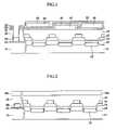
- FIG. 1is a cross-sectional view illustrating a CMOS image sensor according to a first embodiment of the present invention
- FIG. 2 to FIG. 8are cross-sectional view illustrating manufacturing steps of the CMOS image sensor according to the first embodiment of the present invention
- FIG. 9is a cross-sectional view illustrating a manufacturing step of a conventional CMOS image sensor in which a green filter is formed by depositing a green photo resist after blue and red color filters are formed;
- FIG. 10is a cross-sectional view illustrating a CMOS image sensor according to a second embodiment of the present invention.
- CMOS image sensor and a manufacturing method thereofaccording to a preferred embodiment of the present invention will be described hereinafter with reference to the accompanying drawings in detail.
- FIG. 1is a cross-section view illustrating a CMOS image sensor according to a first embodiment of the present invention
- the CMOS image sensor according to the first embodiment of the present inventionincludes a field oxide layer 12 formed on a semiconductor substrate 11 for electrically isolating the devices from each other.
- a gate electrode (not shown) of a transistormade by depositing polysilicon and tungsten silicide, is formed.
- a light receiving area comprised of photodiodes 13is formed in the semiconductor substrate 11 and a source and a drain of the transistor and a sensing node (not shown) are formed by ion implanting.
- an interlayer insulating film 14 and metal wiring 15are sequentially formed, and a pad part 50 is formed with the metal wiring from the same layer, the metal wiring being connected to an exterior circuit.
- a protection layer 16is formed on the metal wiring 15 and the pad part 50 .
- three color filtersi.e. red filter 18 , green filter 19 , and blue filter 20 , for implementing color image are formed on the protection layer 16 .
- the three color filtersare 18 , 19 , and 20 are typically formed using dyed photo resists.
- the blue color filter 18is formed on the protection layer 16 , and a first isolation layer 21 is formed on the blue color filter 18 and the protection layer 16 .
- the red color filter 19is formed on the first isolation layer 21 on which the blue color filter 18 is not formed, and the second isolation layer 22 is formed on the red color filter 19 and the first isolation layer 21 .
- the green color filter 20is formed on the second isolation layer 22 on which the blue color filter 18 and the red color filter are not formed.
- a third isolation layer 23is formed on the green color filter 20 and the second dielectric filter 22 .
- Each of the first to third isolation layersis any of thermal silicon oxide, silicon nitride, TEOS, silicon oxide layer, silicon oxide nitride layer.
- the blue color filter 18 , the red color filter 19 , and the green color filter 20are deposited in sequential order, however, the color filters can be deposited in different orders.
- a field oxide layer 12is formed on the semiconductor substrate for isolating devices from each other and then a gate electrode (not shown) of a transistor is formed by depositing polysilicon and tungsten silicide on the semiconductor substrate.
- the interlayer insulating film 14 and the metal wiring 15are formed in sequential order on the semiconductor substrate, and the pad part 50 is preferably formed so as to connect to the exterior circuit. And then the protection layer 16 is formed on the metal wiring 15 .
- inter metaldielectricIMD is formed between the metal wiring and the first protection layer is formed on the final metal wiring even though a single metal wiring is illustrated in FIG. 2 .
- a blue photo resist 18 ais formed on the protection layer 16 .
- the blue photo resist 18 ais exposed and developed so as to be formed as the blue color filter, and then the first transparent isolation layer 21 is formed on the blue color filter and the protection layer 16 .
- the first isolation layer 21is one of thermal oxide layer, silicon nitride layer, TEOS, silicon oxide layer and silicon oxide nitride layer.
- the first isolation layer 21is formed at a thickness in the range of 50 ⁇ 3000 ⁇ , particularly at 1000 ⁇ using the chemical vapor deposition or the spin coating technique.
- the red photo resist 19 ais formed on the first isolation layer 21 .
- the red photo resist 19 ais exposed and developed so as to be formed as the red color filter 19 , and the second transparent isolation layer 22 is formed on the red color filter 19 and the first isolation layer 21 .
- the second isolation layer 22is one of thermal oxide layer, silicon nitride layer, TEOS, silicon oxide layer and silicon oxide nitride layer.
- the green photo resist 20 ais formed on the second isolation layer 22 .
- the green photo resist 20 ais exposed and developed so as to be formed as the green color filter 20 , and the third transparent isolation layer 23 is formed on the green color filter 20 and the second isolation layer 22 .
- the previously formed blue and red filters 18 and 19should be removed together with the green photo resist since there is no isolation layer which is applied to the first embodiment of the present invention. Accordingly, the rework should be performed from the initial blue color filter formation process. That is, in order to forming a single color filter in rework process, the previously formed color filters should be removed.
- the isolation layers 21 , 22 , and 23are formed between the respective color filters such that it is possible to perform the green color filter formation rework without removing the blue and red color filters 18 and 19 since the blue and red color filters 18 and 19 are protected by the second isolation layer 22 .
- the isolation layers 21 , 22 , and 23 and the protection layer 16are etched using the pad pattern 24 as a mask so as to expose the pad part 50 . And then the pad pattern 24 is removed by ashing technique.
- the color filteris formed after the pad part 50 is formed such that the pad part 50 is likely to be eroded by the developer solution and the erosion damage can be deteriorated when the rework is required.
- the pad part 50is protected by the first to third isolation layers 21 , 22 , and 23 and the pad part 50 is exposed after the color filters are completely formed such that the pad part 50 and the color filters 18 , 19 , and 20 can be protected during the etching process for exposing the pad part 50 and the ashing process for removing the pad photo resist.
- FIG. 10is a cross-sectional view illustrating a CMOS image sensor according two a second embodiment of the present invention.
- the identical reference numeralsrefer to the similar functions and members in the previous drawings.
- the blue filter 18is formed on the protection layer 16
- the first isolation layer 21is formed on the blue color filter 18 and the protection layer 16
- the red filter 19 and the green filter 20are formed on the first isolation layer 21 so as not to be overlapped with the blue color filter 18 and from each other.
- the processcan be simplified by skipping the second isolation layer formation process. Also, by canceling the formation of the second isolation layer which is formed by depositing the thermal oxide layer, it is possible to minimize the performance degradation of the image sensor caused by the heat generated during the thermal oxide layer formation process.
- the third isolation layer 23is formed on the red and green color filters 19 and 20 and the first isolation layer 21 .
- the isolation layers 21 and 23are formed between the color filters such that even when the rework for any of color filters formation processes, for example the red filter formation process, is required, there is no need to remove the blue color filter 18 which is protected by the first isolation layer 21 .
- the blue color filter 18 , the red color filter 19 , and the green color filter 20are deposited in sequential order, however, the deposition order can be changed.
- the isolation layersare provided between the color filters such that it is possible to protect the previously formed color filter(s) during the rework process.
- the pad part metalis exposed after forming the color filters, it is possible to prevent the pad part from being damaged.
Landscapes
- Solid State Image Pick-Up Elements (AREA)
Abstract
Description
Claims (20)
Applications Claiming Priority (2)
| Application Number | Priority Date | Filing Date | Title |
|---|---|---|---|
| KR1020030068493AKR20050032438A (en) | 2003-10-01 | 2003-10-01 | Cmos image sensor and manufacturing method thereof |
| KR10-2003-0068493 | 2003-10-01 |
Publications (2)
| Publication Number | Publication Date |
|---|---|
| US20050082627A1 US20050082627A1 (en) | 2005-04-21 |
| US7129108B2true US7129108B2 (en) | 2006-10-31 |
Family
ID=34510849
Family Applications (1)
| Application Number | Title | Priority Date | Filing Date |
|---|---|---|---|
| US10/956,202Expired - Fee RelatedUS7129108B2 (en) | 2003-10-01 | 2004-09-30 | CMOS image sensor and manufacturing method thereof |
Country Status (2)
| Country | Link |
|---|---|
| US (1) | US7129108B2 (en) |
| KR (1) | KR20050032438A (en) |
Cited By (11)
| Publication number | Priority date | Publication date | Assignee | Title |
|---|---|---|---|---|
| US20070065972A1 (en)* | 2005-09-22 | 2007-03-22 | Samsung Electronics Co., Ltd. | Image sensor and method of making same |
| US20090072285A1 (en)* | 2007-09-19 | 2009-03-19 | Jong-Taek Hwang | Cmos image sensor and method for fabricating the same |
| US20120077300A1 (en)* | 2004-12-08 | 2012-03-29 | Canon Kabushiki Kaisha | Photoelectric conversion device and method for producing photoelectric conversion device |
| US8466000B2 (en) | 2011-04-14 | 2013-06-18 | United Microelectronics Corp. | Backside-illuminated image sensor and fabricating method thereof |
| US20130180949A1 (en)* | 2012-01-13 | 2013-07-18 | Fu-Tien Weng | Color filter structure and method for fabricating the same |
| US9343489B2 (en) | 2011-05-12 | 2016-05-17 | DePuy Synthes Products, Inc. | Image sensor for endoscopic use |
| US9462234B2 (en) | 2012-07-26 | 2016-10-04 | DePuy Synthes Products, Inc. | Camera system with minimal area monolithic CMOS image sensor |
| US9509917B2 (en) | 2012-07-26 | 2016-11-29 | DePuy Synthes Products, Inc. | Wide dynamic range using monochromatic sensor |
| US10206561B2 (en) | 2013-02-28 | 2019-02-19 | DePuy Synthes Products, Inc. | Videostroboscopy of vocal cords with CMOS sensors |
| US10517469B2 (en) | 2013-03-15 | 2019-12-31 | DePuy Synthes Products, Inc. | Image sensor synchronization without input clock and data transmission clock |
| US10750933B2 (en) | 2013-03-15 | 2020-08-25 | DePuy Synthes Products, Inc. | Minimize image sensor I/O and conductor counts in endoscope applications |
Families Citing this family (2)
| Publication number | Priority date | Publication date | Assignee | Title |
|---|---|---|---|---|
| US7453109B2 (en)* | 2004-09-03 | 2008-11-18 | Canon Kabushiki Kaisha | Solid-state image sensor and imaging system |
| US8921905B2 (en) | 2012-10-16 | 2014-12-30 | Unisantis Electronics Singapore Pte. Ltd. | Solid-state imaging device |
Citations (10)
| Publication number | Priority date | Publication date | Assignee | Title |
|---|---|---|---|---|
| US4600833A (en) | 1982-03-29 | 1986-07-15 | Mitsubishi Denki Kabushiki Kaisha | Solid state image sensing device with a color filter |
| JPH023968A (en) | 1988-06-20 | 1990-01-09 | Nec Corp | Manufacture of solid-state colored image sensing element |
| US5719074A (en) | 1995-11-07 | 1998-02-17 | Eastman Kodak Company | Method of making a planar color filter array for CCDS from dyed and mordant layers |
| US5841126A (en) | 1994-01-28 | 1998-11-24 | California Institute Of Technology | CMOS active pixel sensor type imaging system on a chip |
| US5886659A (en) | 1996-08-21 | 1999-03-23 | California Institute Of Technology | On-focal-plane analog-to-digital conversion for current-mode imaging devices |
| US5990506A (en) | 1996-03-20 | 1999-11-23 | California Institute Of Technology | Active pixel sensors with substantially planarized color filtering elements |
| US6005619A (en) | 1997-10-06 | 1999-12-21 | Photobit Corporation | Quantum efficiency improvements in active pixel sensors |
| US6021172A (en) | 1994-01-28 | 2000-02-01 | California Institute Of Technology | Active pixel sensor having intra-pixel charge transfer with analog-to-digital converter |
| US20030071271A1 (en)* | 1999-12-02 | 2003-04-17 | Satoshi Suzuki | Solid-state image sensor, production method of the same, and digital camera |
| US6852565B1 (en)* | 2003-07-10 | 2005-02-08 | Galaxcore, Inc. | CMOS image sensor with substrate noise barrier |
- 2003
- 2003-10-01KRKR1020030068493Apatent/KR20050032438A/ennot_activeCeased
- 2004
- 2004-09-30USUS10/956,202patent/US7129108B2/ennot_activeExpired - Fee Related
Patent Citations (10)
| Publication number | Priority date | Publication date | Assignee | Title |
|---|---|---|---|---|
| US4600833A (en) | 1982-03-29 | 1986-07-15 | Mitsubishi Denki Kabushiki Kaisha | Solid state image sensing device with a color filter |
| JPH023968A (en) | 1988-06-20 | 1990-01-09 | Nec Corp | Manufacture of solid-state colored image sensing element |
| US5841126A (en) | 1994-01-28 | 1998-11-24 | California Institute Of Technology | CMOS active pixel sensor type imaging system on a chip |
| US6021172A (en) | 1994-01-28 | 2000-02-01 | California Institute Of Technology | Active pixel sensor having intra-pixel charge transfer with analog-to-digital converter |
| US5719074A (en) | 1995-11-07 | 1998-02-17 | Eastman Kodak Company | Method of making a planar color filter array for CCDS from dyed and mordant layers |
| US5990506A (en) | 1996-03-20 | 1999-11-23 | California Institute Of Technology | Active pixel sensors with substantially planarized color filtering elements |
| US5886659A (en) | 1996-08-21 | 1999-03-23 | California Institute Of Technology | On-focal-plane analog-to-digital conversion for current-mode imaging devices |
| US6005619A (en) | 1997-10-06 | 1999-12-21 | Photobit Corporation | Quantum efficiency improvements in active pixel sensors |
| US20030071271A1 (en)* | 1999-12-02 | 2003-04-17 | Satoshi Suzuki | Solid-state image sensor, production method of the same, and digital camera |
| US6852565B1 (en)* | 2003-07-10 | 2005-02-08 | Galaxcore, Inc. | CMOS image sensor with substrate noise barrier |
Non-Patent Citations (1)
| Title |
|---|
| Satoshi Uchiya; Manufacture of Solid-State Colored Image Sensing Element; Patent Abstracts of Japan; Publication No. 02-003968; Publication Date Jan. 9, 1990; 1 Pg.; Japan Patent Office; 1998, 2003. |
Cited By (50)
| Publication number | Priority date | Publication date | Assignee | Title |
|---|---|---|---|---|
| US9490286B2 (en) | 2004-12-08 | 2016-11-08 | Canon Kabushiki Kaisha | Photoelectric conversion device and method for producing photoelectric conversion device |
| US20120077300A1 (en)* | 2004-12-08 | 2012-03-29 | Canon Kabushiki Kaisha | Photoelectric conversion device and method for producing photoelectric conversion device |
| US10367030B2 (en) | 2004-12-08 | 2019-07-30 | Canon Kabushiki Kaisha | Photoelectric conversion device and method for producing photoelectric conversion device |
| US8790952B2 (en)* | 2004-12-08 | 2014-07-29 | Canon Kabushiki Kaisha | Photoelectric conversion device and method for producing photoelectric conversion device |
| US9818793B2 (en) | 2004-12-08 | 2017-11-14 | Canon Kabushiki Kaisha | Photoelectric conversion device and method for producing photoelectric conversion device |
| US7919350B2 (en)* | 2005-09-22 | 2011-04-05 | Samsung Electronics Co., Ltd. | Image sensor and method of making same |
| US20070065972A1 (en)* | 2005-09-22 | 2007-03-22 | Samsung Electronics Co., Ltd. | Image sensor and method of making same |
| US20090072285A1 (en)* | 2007-09-19 | 2009-03-19 | Jong-Taek Hwang | Cmos image sensor and method for fabricating the same |
| US7919351B2 (en)* | 2007-09-19 | 2011-04-05 | Dongbu Hitek Co., Ltd. | CMOS image sensor with multi-layered planarization layer and method for fabricating the same |
| US8466000B2 (en) | 2011-04-14 | 2013-06-18 | United Microelectronics Corp. | Backside-illuminated image sensor and fabricating method thereof |
| US11179029B2 (en) | 2011-05-12 | 2021-11-23 | DePuy Synthes Products, Inc. | Image sensor with tolerance optimizing interconnects |
| US10537234B2 (en) | 2011-05-12 | 2020-01-21 | DePuy Synthes Products, Inc. | Image sensor with tolerance optimizing interconnects |
| US11432715B2 (en) | 2011-05-12 | 2022-09-06 | DePuy Synthes Products, Inc. | System and method for sub-column parallel digitizers for hybrid stacked image sensor using vertical interconnects |
| US11109750B2 (en) | 2011-05-12 | 2021-09-07 | DePuy Synthes Products, Inc. | Pixel array area optimization using stacking scheme for hybrid image sensor with minimal vertical interconnects |
| US9622650B2 (en) | 2011-05-12 | 2017-04-18 | DePuy Synthes Products, Inc. | System and method for sub-column parallel digitizers for hybrid stacked image sensor using vertical interconnects |
| US9763566B2 (en) | 2011-05-12 | 2017-09-19 | DePuy Synthes Products, Inc. | Pixel array area optimization using stacking scheme for hybrid image sensor with minimal vertical interconnects |
| US9343489B2 (en) | 2011-05-12 | 2016-05-17 | DePuy Synthes Products, Inc. | Image sensor for endoscopic use |
| US9907459B2 (en) | 2011-05-12 | 2018-03-06 | DePuy Synthes Products, Inc. | Image sensor with tolerance optimizing interconnects |
| US9980633B2 (en) | 2011-05-12 | 2018-05-29 | DePuy Synthes Products, Inc. | Image sensor for endoscopic use |
| US11026565B2 (en) | 2011-05-12 | 2021-06-08 | DePuy Synthes Products, Inc. | Image sensor for endoscopic use |
| US11848337B2 (en) | 2011-05-12 | 2023-12-19 | DePuy Synthes Products, Inc. | Image sensor |
| US10863894B2 (en) | 2011-05-12 | 2020-12-15 | DePuy Synthes Products, Inc. | System and method for sub-column parallel digitizers for hybrid stacked image sensor using vertical interconnects |
| US10709319B2 (en) | 2011-05-12 | 2020-07-14 | DePuy Synthes Products, Inc. | System and method for sub-column parallel digitizers for hybrid stacked image sensor using vertical interconnects |
| US12100716B2 (en) | 2011-05-12 | 2024-09-24 | DePuy Synthes Products, Inc. | Image sensor with tolerance optimizing interconnects |
| US10517471B2 (en) | 2011-05-12 | 2019-12-31 | DePuy Synthes Products, Inc. | Pixel array area optimization using stacking scheme for hybrid image sensor with minimal vertical interconnects |
| US11682682B2 (en) | 2011-05-12 | 2023-06-20 | DePuy Synthes Products, Inc. | Pixel array area optimization using stacking scheme for hybrid image sensor with minimal vertical interconnects |
| US20130180949A1 (en)* | 2012-01-13 | 2013-07-18 | Fu-Tien Weng | Color filter structure and method for fabricating the same |
| US8664680B2 (en)* | 2012-01-13 | 2014-03-04 | Visera Technologies Company Limited | Color filter structure and method for fabricating the same |
| US11766175B2 (en) | 2012-07-26 | 2023-09-26 | DePuy Synthes Products, Inc. | Camera system with minimal area monolithic CMOS image sensor |
| US11089192B2 (en) | 2012-07-26 | 2021-08-10 | DePuy Synthes Products, Inc. | Camera system with minimal area monolithic CMOS image sensor |
| US9509917B2 (en) | 2012-07-26 | 2016-11-29 | DePuy Synthes Products, Inc. | Wide dynamic range using monochromatic sensor |
| US11751757B2 (en) | 2012-07-26 | 2023-09-12 | DePuy Synthes Products, Inc. | Wide dynamic range using monochromatic sensor |
| US10165195B2 (en) | 2012-07-26 | 2018-12-25 | DePuy Synthes Products, Inc. | Wide dynamic range using monochromatic sensor |
| US10075626B2 (en) | 2012-07-26 | 2018-09-11 | DePuy Synthes Products, Inc. | Camera system with minimal area monolithic CMOS image sensor |
| US11082627B2 (en) | 2012-07-26 | 2021-08-03 | DePuy Synthes Products, Inc. | Wide dynamic range using monochromatic sensor |
| US9462234B2 (en) | 2012-07-26 | 2016-10-04 | DePuy Synthes Products, Inc. | Camera system with minimal area monolithic CMOS image sensor |
| US9621817B2 (en) | 2012-07-26 | 2017-04-11 | DePuy Synthes Products, Inc. | Wide dynamic range using monochromatic sensor |
| US10742895B2 (en) | 2012-07-26 | 2020-08-11 | DePuy Synthes Products, Inc. | Wide dynamic range using monochromatic sensor |
| US10701254B2 (en) | 2012-07-26 | 2020-06-30 | DePuy Synthes Products, Inc. | Camera system with minimal area monolithic CMOS image sensor |
| US11266305B2 (en) | 2013-02-28 | 2022-03-08 | DePuy Synthes Products, Inc. | Videostroboscopy of vocal cords with CMOS sensors |
| US11998166B2 (en) | 2013-02-28 | 2024-06-04 | DePuy Synthes Products, Inc. | Videostroboscopy of vocal cords with CMOS sensors |
| US10206561B2 (en) | 2013-02-28 | 2019-02-19 | DePuy Synthes Products, Inc. | Videostroboscopy of vocal cords with CMOS sensors |
| US10750933B2 (en) | 2013-03-15 | 2020-08-25 | DePuy Synthes Products, Inc. | Minimize image sensor I/O and conductor counts in endoscope applications |
| US11344189B2 (en) | 2013-03-15 | 2022-05-31 | DePuy Synthes Products, Inc. | Image sensor synchronization without input clock and data transmission clock |
| US11253139B2 (en) | 2013-03-15 | 2022-02-22 | DePuy Synthes Products, Inc. | Minimize image sensor I/O and conductor counts in endoscope applications |
| US10980406B2 (en) | 2013-03-15 | 2021-04-20 | DePuy Synthes Products, Inc. | Image sensor synchronization without input clock and data transmission clock |
| US11903564B2 (en) | 2013-03-15 | 2024-02-20 | DePuy Synthes Products, Inc. | Image sensor synchronization without input clock and data transmission clock |
| US10881272B2 (en) | 2013-03-15 | 2021-01-05 | DePuy Synthes Products, Inc. | Minimize image sensor I/O and conductor counts in endoscope applications |
| US10517469B2 (en) | 2013-03-15 | 2019-12-31 | DePuy Synthes Products, Inc. | Image sensor synchronization without input clock and data transmission clock |
| US12150620B2 (en) | 2013-03-15 | 2024-11-26 | DePuy Synthes Products, Inc. | Minimize image sensor I/O and conductor counts in endoscope applications |
Also Published As
| Publication number | Publication date |
|---|---|
| US20050082627A1 (en) | 2005-04-21 |
| KR20050032438A (en) | 2005-04-07 |
Similar Documents
| Publication | Publication Date | Title |
|---|---|---|
| US7232698B2 (en) | Method for fabricating CMOS image sensor protecting low temperature oxide delamination | |
| US7498190B2 (en) | Method for fabricating a CMOS image sensor | |
| US6379992B2 (en) | Method for fabricating an image sensor | |
| US7268009B2 (en) | Method for fabricating a CMOS image sensor | |
| US7859072B2 (en) | Image sensor and method for manufacturing the same | |
| US7129108B2 (en) | CMOS image sensor and manufacturing method thereof | |
| KR20010061308A (en) | Method for fabricating thin film image sensor | |
| US7879640B2 (en) | CMOS image sensor and method for fabricating the same | |
| KR100461977B1 (en) | CMOS image sensor and fabricating method of the same | |
| KR100449951B1 (en) | Image sensor and method of fabricating the same | |
| KR100595601B1 (en) | CMOS image sensor manufacturing method | |
| KR20010061343A (en) | Method for fabricating image sensor | |
| KR100660323B1 (en) | Manufacturing Method of CMOS Image Sensor | |
| KR20050011955A (en) | Fabricating method of cmos image sensor with protecting microlense capping layer lifting | |
| KR100440774B1 (en) | Image sensor with Light shield layer | |
| US6846705B2 (en) | Method for fabricating complementary metal oxide semiconductor image sensor having redundancy module | |
| KR20050011951A (en) | Fabricating method of cmos image sensor with protecting microlense capping layer lifting | |
| KR20030001066A (en) | Method for fabricating light detecting device | |
| KR100800757B1 (en) | How to prevent metal pad oxidation in the image sensor | |
| KR100989987B1 (en) | Manufacturing method of CMOS image sensor preventing the peeling phenomenon of overcoating layer | |
| KR20030042305A (en) | The method of fabrication for CMOS image sensor | |
| KR100880529B1 (en) | Color filter of CMOS image sensor and its manufacturing method | |
| KR100707072B1 (en) | Color filter formation method of image sensor | |
| KR101024739B1 (en) | Image sensor and manufacturing method of image sensor | |
| KR100720463B1 (en) | Manufacturing Method of CMOS Image Sensor |
Legal Events
| Date | Code | Title | Description |
|---|---|---|---|
| AS | Assignment | Owner name:DONGBU ELECTRONICS CO., LTD., KOREA, REPUBLIC OF Free format text:ASSIGNMENT OF ASSIGNORS INTEREST;ASSIGNOR:JANG, HOON;REEL/FRAME:015871/0372 Effective date:20040910 | |
| AS | Assignment | Owner name:DONGBUANAM SEMICONDUCTOR INC., KOREA, REPUBLIC OF Free format text:MERGER;ASSIGNOR:DONGBU ELECTRONICS CO., LTD;REEL/FRAME:016292/0146 Effective date:20041221 | |
| AS | Assignment | Owner name:DONGBU ELECTRONICS CO., LTD.,KOREA, REPUBLIC OF Free format text:CHANGE OF NAME;ASSIGNOR:DONGANAM SEMICONDUCTOR INC.;REEL/FRAME:017749/0335 Effective date:20060328 Owner name:DONGBU ELECTRONICS CO., LTD., KOREA, REPUBLIC OF Free format text:CHANGE OF NAME;ASSIGNOR:DONGANAM SEMICONDUCTOR INC.;REEL/FRAME:017749/0335 Effective date:20060328 | |
| AS | Assignment | Owner name:DONGBU ELECTRONICS CO., LTD., KOREA, REPUBLIC OF Free format text:CORRECTIVE ASSIGNMENT TO CORRECT THE ASSIGNOR PREVIOUSLY RECORDED ON REEL 017749 FRAME 0335;ASSIGNOR:DONGBUANAM SEMICONDUCTOR INC.;REEL/FRAME:017821/0670 Effective date:20060328 Owner name:DONGBU ELECTRONICS CO., LTD.,KOREA, REPUBLIC OF Free format text:CORRECTIVE ASSIGNMENT TO CORRECT THE ASSIGNOR PREVIOUSLY RECORDED ON REEL 017749 FRAME 0335. ASSIGNOR(S) HEREBY CONFIRMS THE ASSIGNOR SHOULD BE "DONGBUANAM SEMICONDUCTOR INC.";ASSIGNOR:DONGBUANAM SEMICONDUCTOR INC.;REEL/FRAME:017821/0670 Effective date:20060328 Owner name:DONGBU ELECTRONICS CO., LTD., KOREA, REPUBLIC OF Free format text:CORRECTIVE ASSIGNMENT TO CORRECT THE ASSIGNOR PREVIOUSLY RECORDED ON REEL 017749 FRAME 0335. ASSIGNOR(S) HEREBY CONFIRMS THE ASSIGNOR SHOULD BE "DONGBUANAM SEMICONDUCTOR INC.";ASSIGNOR:DONGBUANAM SEMICONDUCTOR INC.;REEL/FRAME:017821/0670 Effective date:20060328 | |
| FEPP | Fee payment procedure | Free format text:PAYOR NUMBER ASSIGNED (ORIGINAL EVENT CODE: ASPN); ENTITY STATUS OF PATENT OWNER: LARGE ENTITY | |
| FPAY | Fee payment | Year of fee payment:4 | |
| FPAY | Fee payment | Year of fee payment:8 | |
| AS | Assignment | Owner name:DONGBU HITEK CO., LTD., KOREA, REPUBLIC OF Free format text:MERGER AND CHANGE OF NAME;ASSIGNORS:DONGBU ELECTRONICS CO., LTD.;DONGBU HITEK CO., LTD.;REEL/FRAME:044533/0523 Effective date:20070503 | |
| AS | Assignment | Owner name:DB HITEK CO., LTD, KOREA, REPUBLIC OF Free format text:CHANGE OF NAME;ASSIGNOR:DONGBU HITEK CO., LTD.;REEL/FRAME:044555/0913 Effective date:20171101 | |
| FEPP | Fee payment procedure | Free format text:MAINTENANCE FEE REMINDER MAILED (ORIGINAL EVENT CODE: REM.) | |
| LAPS | Lapse for failure to pay maintenance fees | Free format text:PATENT EXPIRED FOR FAILURE TO PAY MAINTENANCE FEES (ORIGINAL EVENT CODE: EXP.); ENTITY STATUS OF PATENT OWNER: LARGE ENTITY | |
| STCH | Information on status: patent discontinuation | Free format text:PATENT EXPIRED DUE TO NONPAYMENT OF MAINTENANCE FEES UNDER 37 CFR 1.362 | |
| FP | Lapsed due to failure to pay maintenance fee | Effective date:20181031 | |
| AS | Assignment | Owner name:COLUMBA TECHNOLOGIES INC., CANADA Free format text:ASSIGNMENT OF ASSIGNORS INTEREST;ASSIGNOR:DB HITEK CO., LTD.;REEL/FRAME:049709/0857 Effective date:20190125 |