US7126738B2 - Visible spectrum modulator arrays - Google Patents
Visible spectrum modulator arraysDownload PDFInfo
- Publication number
- US7126738B2 US7126738B2US10/082,397US8239702AUS7126738B2US 7126738 B2US7126738 B2US 7126738B2US 8239702 AUS8239702 AUS 8239702AUS 7126738 B2US7126738 B2US 7126738B2
- Authority
- US
- United States
- Prior art keywords
- cavity
- mirror
- layer
- light
- modulation
- Prior art date
- Legal status (The legal status is an assumption and is not a legal conclusion. Google has not performed a legal analysis and makes no representation as to the accuracy of the status listed.)
- Expired - Fee Related
Links
Images


Classifications
- G—PHYSICS
- G02—OPTICS
- G02B—OPTICAL ELEMENTS, SYSTEMS OR APPARATUS
- G02B26/00—Optical devices or arrangements for the control of light using movable or deformable optical elements
- G02B26/001—Optical devices or arrangements for the control of light using movable or deformable optical elements based on interference in an adjustable optical cavity
- B—PERFORMING OPERATIONS; TRANSPORTING
- B82—NANOTECHNOLOGY
- B82Y—SPECIFIC USES OR APPLICATIONS OF NANOSTRUCTURES; MEASUREMENT OR ANALYSIS OF NANOSTRUCTURES; MANUFACTURE OR TREATMENT OF NANOSTRUCTURES
- B82Y20/00—Nanooptics, e.g. quantum optics or photonic crystals
- G—PHYSICS
- G02—OPTICS
- G02B—OPTICAL ELEMENTS, SYSTEMS OR APPARATUS
- G02B26/00—Optical devices or arrangements for the control of light using movable or deformable optical elements
- G02B26/08—Optical devices or arrangements for the control of light using movable or deformable optical elements for controlling the direction of light
- G—PHYSICS
- G02—OPTICS
- G02F—OPTICAL DEVICES OR ARRANGEMENTS FOR THE CONTROL OF LIGHT BY MODIFICATION OF THE OPTICAL PROPERTIES OF THE MEDIA OF THE ELEMENTS INVOLVED THEREIN; NON-LINEAR OPTICS; FREQUENCY-CHANGING OF LIGHT; OPTICAL LOGIC ELEMENTS; OPTICAL ANALOGUE/DIGITAL CONVERTERS
- G02F1/00—Devices or arrangements for the control of the intensity, colour, phase, polarisation or direction of light arriving from an independent light source, e.g. switching, gating or modulating; Non-linear optics
- G02F1/01—Devices or arrangements for the control of the intensity, colour, phase, polarisation or direction of light arriving from an independent light source, e.g. switching, gating or modulating; Non-linear optics for the control of the intensity, phase, polarisation or colour
- G02F1/19—Devices or arrangements for the control of the intensity, colour, phase, polarisation or direction of light arriving from an independent light source, e.g. switching, gating or modulating; Non-linear optics for the control of the intensity, phase, polarisation or colour based on variable-reflection or variable-refraction elements not provided for in groups G02F1/015 - G02F1/169
- G—PHYSICS
- G09—EDUCATION; CRYPTOGRAPHY; DISPLAY; ADVERTISING; SEALS
- G09G—ARRANGEMENTS OR CIRCUITS FOR CONTROL OF INDICATING DEVICES USING STATIC MEANS TO PRESENT VARIABLE INFORMATION
- G09G3/00—Control arrangements or circuits, of interest only in connection with visual indicators other than cathode-ray tubes
- G09G3/20—Control arrangements or circuits, of interest only in connection with visual indicators other than cathode-ray tubes for presentation of an assembly of a number of characters, e.g. a page, by composing the assembly by combination of individual elements arranged in a matrix no fixed position being assigned to or needed to be assigned to the individual characters or partial characters
- G09G3/22—Control arrangements or circuits, of interest only in connection with visual indicators other than cathode-ray tubes for presentation of an assembly of a number of characters, e.g. a page, by composing the assembly by combination of individual elements arranged in a matrix no fixed position being assigned to or needed to be assigned to the individual characters or partial characters using controlled light sources
- G—PHYSICS
- G09—EDUCATION; CRYPTOGRAPHY; DISPLAY; ADVERTISING; SEALS
- G09G—ARRANGEMENTS OR CIRCUITS FOR CONTROL OF INDICATING DEVICES USING STATIC MEANS TO PRESENT VARIABLE INFORMATION
- G09G3/00—Control arrangements or circuits, of interest only in connection with visual indicators other than cathode-ray tubes
- G09G3/20—Control arrangements or circuits, of interest only in connection with visual indicators other than cathode-ray tubes for presentation of an assembly of a number of characters, e.g. a page, by composing the assembly by combination of individual elements arranged in a matrix no fixed position being assigned to or needed to be assigned to the individual characters or partial characters
- G09G3/34—Control arrangements or circuits, of interest only in connection with visual indicators other than cathode-ray tubes for presentation of an assembly of a number of characters, e.g. a page, by composing the assembly by combination of individual elements arranged in a matrix no fixed position being assigned to or needed to be assigned to the individual characters or partial characters by control of light from an independent source
- G09G3/3433—Control arrangements or circuits, of interest only in connection with visual indicators other than cathode-ray tubes for presentation of an assembly of a number of characters, e.g. a page, by composing the assembly by combination of individual elements arranged in a matrix no fixed position being assigned to or needed to be assigned to the individual characters or partial characters by control of light from an independent source using light modulating elements actuated by an electric field and being other than liquid crystal devices and electrochromic devices
- G09G3/3466—Control arrangements or circuits, of interest only in connection with visual indicators other than cathode-ray tubes for presentation of an assembly of a number of characters, e.g. a page, by composing the assembly by combination of individual elements arranged in a matrix no fixed position being assigned to or needed to be assigned to the individual characters or partial characters by control of light from an independent source using light modulating elements actuated by an electric field and being other than liquid crystal devices and electrochromic devices based on interferometric effect
- G—PHYSICS
- G09—EDUCATION; CRYPTOGRAPHY; DISPLAY; ADVERTISING; SEALS
- G09G—ARRANGEMENTS OR CIRCUITS FOR CONTROL OF INDICATING DEVICES USING STATIC MEANS TO PRESENT VARIABLE INFORMATION
- G09G2300/00—Aspects of the constitution of display devices
- G09G2300/04—Structural and physical details of display devices
- G09G2300/0439—Pixel structures
- G09G2300/0456—Pixel structures with a reflective area and a transmissive area combined in one pixel, such as in transflectance pixels
- G—PHYSICS
- G09—EDUCATION; CRYPTOGRAPHY; DISPLAY; ADVERTISING; SEALS
- G09G—ARRANGEMENTS OR CIRCUITS FOR CONTROL OF INDICATING DEVICES USING STATIC MEANS TO PRESENT VARIABLE INFORMATION
- G09G2330/00—Aspects of power supply; Aspects of display protection and defect management
- G09G2330/02—Details of power systems and of start or stop of display operation
- G09G2330/021—Power management, e.g. power saving
- G—PHYSICS
- G09—EDUCATION; CRYPTOGRAPHY; DISPLAY; ADVERTISING; SEALS
- G09G—ARRANGEMENTS OR CIRCUITS FOR CONTROL OF INDICATING DEVICES USING STATIC MEANS TO PRESENT VARIABLE INFORMATION
- G09G3/00—Control arrangements or circuits, of interest only in connection with visual indicators other than cathode-ray tubes
- G09G3/20—Control arrangements or circuits, of interest only in connection with visual indicators other than cathode-ray tubes for presentation of an assembly of a number of characters, e.g. a page, by composing the assembly by combination of individual elements arranged in a matrix no fixed position being assigned to or needed to be assigned to the individual characters or partial characters
- G09G3/2007—Display of intermediate tones
- G09G3/2014—Display of intermediate tones by modulation of the duration of a single pulse during which the logic level remains constant
Definitions
- This inventionrelates to visible spectrum (including ultra-violet and infrared) modulator arrays.
- Visible spectrum modulator arrayssuch as backlit LCD computer screens, have arrays of electro-optical elements corresponding to pixels. Each element may be electronically controlled to alter light which is aimed to pass through the element. By controlling all of the elements of the array, black and white or, using appropriate elements, color images may be displayed. Non-backlit LCD arrays have similar properties but work on reflected light. These and other types of visible spectrum modulator arrays have a wide variety of other uses.
- the inventionfeatures modulation of light in the visible spectrum using an array of modulation elements, and control circuitry connected to the array for controlling each of the modulation elements independently, each of the modulation elements having a surface which is caused to exhibit a predetermined impedance characteristic to particular frequencies of light.
- the surfacemay include antennas configured to interact with selected frequencies of light, or the surface may be a surface of an interference cavity.
- the impedance characteristicmay be reflection of particular frequencies of light, or transmission of particular frequencies of light.
- Each of the modulation elementsmay be an interference cavity that is deformable to alter the cavity dimension.
- the interference cavitymay include a pair of cavity walls (e.g., mirrors) separated by a cavity dimension.
- One of the mirrorsmay be a broadband mirror and the other of the mirrors may be a narrow band mirror. Or both of the mirrors may be narrow band mirrors, or both of the mirrors may be broad band, non-metallic mirrors.
- the cavitymay have a cavity dimension that renders the cavity resonant with respect to light of the frequency defined by the spectral characteristics of the mirrors and intrinsic cavity spacing in an undeformed state.
- One of the mirrorsmay be a hybrid filter.
- One (or both) of the wallsmay be a dielectric material, a metallic material, or a composite dielectric/metallic material.
- the cavitymay be deformable by virtue of a wall that is under tensile stress.
- the control circuitrymay be connected for analog control of the impedance to light of each element. The analog control may be control of the degree of deformity of the deformable wall of the cavity.
- the predetermined impedance characteristicmay include reflection of incident electromagnetic radiation in the visible spectrum, e.g., the proportion of incident electromagnetic radiation of a given frequency band that is, on average, reflected by each of the modulation elements.
- the modulation elementmay be responsive to a particular electrical condition to occupy either a state of higher reflectivity or a state of lower reflectivity, and the control circuitry may generate a stream of pulses having a duty cycle corresponding to the proportion of incident radiation that is reflected and places the modulation element in the higher state of reflectivity during each the pulse and in the lower state of reflectivity in the intervals between the pulses.
- the characteristicmay include emission of electromagnetic radiation in the visible spectrum.
- the characteristicmay include the amount of electromagnetic radiation in the visible spectrum that is emitted, on average, by the antennas.
- the characteristicmay be incident electromagnetic radiation in the visible spectrum.
- the modulation elementsmay include three sub-elements each associated with one of three colors of the visible spectrum.
- the modulation elementmay be responsive to a particular electrical condition to occupy either a state of higher transmissivity or a state of lower transmissivity, and the control circuitry may generate a stream of pulses having a duty cycle corresponding to the proportion of incident radiation that is transmitted and places the modulation element in the higher state of transmissivity during each the pulse and in the lower state of transmissivity in the intervals between the pulses.
- the characteristicmay include the proportion of incident electromagnetic radiation of a given frequency band that is, on average, transmitted by each of the modulation elements.
- the visible spectrummay include ultraviolet frequencies, or infrared frequencies.
- control circuitrymay be connected to the array for controlling the amplitude of light delivered by each of the modulation elements independently by pulse code modulation.
- the inventionfeatures a modulation element having a deformable portion held under tensile stress, and control circuitry connected to control the deformation of the deformable portion.
- Implementations of the inventionmay include the following features.
- the modulation elementmay be self-supporting or held on separate supports.
- the deformable portionmay be a rectangular membrane supported along two opposite edges by supports which are orthogonal to the membrane.
- the deformable portionunder one mode of control by the control circuitry, may be collapsed onto a wall of the cavity.
- the control circuitrycontrols the deformable portion by signals applied to the modulation element, and the deformation of the control portion may be subject to hysteresis with respect to signals applied by the control circuitry.
- the inventionfeatures modulating light in the visible spectrum using a deformable modulation element having a deformation mechanism and an optical portion, the deformation mechanism and the optical portion independently imparting to the element respectively a controlled deformation characteristic and a controlled modulation characteristic.
- the deformation mechanismmay be a flexible membrane held in tensile stress, and the optical portion may be formed on the flexible membrane.
- the optical portionmay be a mirror.
- the mirrormay have a narrow band, or a broad band, or include a hybrid filter.
- the inventionbroadly features a non-metal deformable modulation element.
- the inventionfeatures a process for making cavity-type modulation elements by forming a sandwich of two layers and a sacrificial layer between them, the sacrificial layer having a thickness related to the final cavity dimension, and using chemical (e.g., water) or a plasma based etch process to remove the sacrificial layer.
- chemicale.g., water
- plasma based etch processto remove the sacrificial layer.
- Very high-resolution, full-color imagesare produced using relatively little power.
- the embodiment which senses the image incident on the arrayhas relatively low noise. Their color response characteristics are tunable by selection of the dimensions of the antennas.
- the antenna or cavity embodimentsare useful in portable, low power, full color displays, especially under high ambient light conditions.
- Phase controlled reflective embodimentsare useful in passive light scanning such as optical disk readers without moving parts.
- the emissive embodimentsalso could be used as display devices especially in low-ambient-light conditions.
- the deviceshave the advantage of being extremely light efficient, making them especially appropriate for high intensity projection displays, and reducing or eliminating the need for backlighting in low ambient light applications.
- more accurate color representationsare possible, as well as designs optimized for the IR and UV.
- Mechanical hysteresisprecludes the need for active drivers, and this coupled with their geometric simplicity and monolithic nature brings defect losses down significantly.
- the devicesare also exceptionally fast, low power, and non-polarizing. The fact that they can be reflective and/or transmissive enhances their flexibility.
- the process for fabrication as represented in some embodimentsrelies on benign chemicals, minimizing waste disposal problems, and facilitating the fabrication of devices on a variety of substrates (e.g., plastics or integrated circuits) using a larger variety of materials.
- substratese.g., plastics or integrated circuits
- Devices on plastic substrateshave the potential of being extremely inexpensive. All of the manufacturing technologies used are mature, further reducing manufacturing costs.
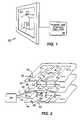
- FIG. 1is a perspective view of a display device.
- FIG. 2is a perspective schematic exploded view of a representative portion of the screen of FIG. 1 .
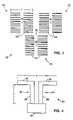
- FIG. 3is an enlarged top view of a tri-dipole of FIG. 2 .
- FIG. 4is a schematic view of a single dipole antenna of FIG. 3 .
- FIG. 5is a schematic perspective view, broken away, of a portion of the screen of FIG. 1 .
- FIG. 6is an enlarged top view of an individual tri-bus of FIG. 2 .
- FIG. 7is an enlarged perspective view of a representative portion of the screen of FIG. 1 .
- FIG. 8is a cross-sectional view along 8 — 8 of FIG. 7 .
- FIG. 9is a diagram of a portion of a control circuit of FIG. 2 , and a corresponding dipole antenna of FIG. 3 .
- FIGS. 10A , 10 B, 10 Care representative graphs of the input voltage to the bias source of FIG. 9 .
- FIG. 11is a diagram of portions of the control modules for a row of pixels
- FIG. 12is a circuit diagram of an oscillator.
- FIG. 13is a schematic diagram of a circuit module of FIG. 2 , a corresponding dipole antenna of FIG. 3 , and a graphical representation of the output of a binary counter.
- FIG. 14is a circuit diagram of the pulse counter of FIG. 13 .
- FIGS. 15 , 16 , 17 , 18 , and 19are top views of alternative dipole arrangements.
- FIGS. 20A through 20Fare perspective views of a cavity devices.
- FIGS. 21A and 21Bare side views of the cavity device.
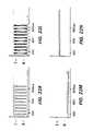
- FIGS. 22A through 22Fare graphs of useful pairs of frequency responses which can be achieved by the cavity device when it is in one of two states.
- FIGS. 22 G through 22 AFare a larger list of graphs of individual frequency responses which in some combinations prove useful in the cavity device.
- FIGS. 23A and 23Bare top and cutaway side views respectively, of a display.
- FIGS. 23C and 23Dare top and cutaway side views, respectively, of another display.
- FIG. 24Ais a graph of an electromechanical response of the cavity device.
- FIGS. 24B and 24Care graphs of addressing and modulation schemes for a display.
- FIG. 24Dis a graph of a hysteresis curve.
- FIGS. 25A through 25N and FIGS. 26A through 26Kare perspective views of the device during assembly.
- FIGS. 27A through 27Care side views of dielectric mirrors.
- FIG. 27Dis a top view of a dielectric mirror.
- FIGS. 28A , 28 Bare perspective and top views of a linear tunable filter.
- FIGS. 29A , 29 Bare perspective and top views of a deformable mirror.
- device 20includes a screen 22 for displaying or sensing a high resolution color image (or a succession of color images) under control of power and control circuitry 26 .
- the imageis made up of a densely packed rectangular array of tiny individual picture elements (pixels) each having a specific hue and brightness corresponding to the part of the image represented by the pixel.
- the pixel density of the imagedepends on the fabrication process used but could be on the order of 100,000 pixels per square centimeter.
- each pixelis generated by one so-called tri-dipole 30 .
- the boundary of each tri-dipoleis T-shaped.
- the tri-dipolesare arranged in rows 32 in an interlocking fashion with the “Ts” of alternating tri-dipoles oriented in one direction and the “Ts” of intervening tri-dipoles along the same row oriented in the opposite direction.
- the rowstogether form a two-dimensional rectangular array of tri-dipoles (corresponding to the array of pixels) that are arranged on a first, external layer 34 of screen 22 .
- the arraymay be called an electrically alterable optical planar array, or a visible spectrum modulator array.
- tri-busses 38are arranged in an interlocking two-dimensional array 40 corresponding to the layout of the tri-dipoles on layer 34 above.
- Each tri-dipole 30is connected to its corresponding tri-bus 38 by a multi-conductor link 42 running from layer 34 to layer 36 in a manner described below.
- a set of circuit modules 46are arranged in a two-dimensional rectangular array corresponding to the layouts of the tri-dipoles and tri-busses.
- Each circuit module 46is connected to its corresponding tri-bus 38 by a six-conductor link 48 running from layer 36 to layer 44 in a manner described below.
- Each circuit module 46electronically controls the optical characteristics of all of the antennas of its corresponding tri-dipole 30 to generate the corresponding pixel of the image on screen 22 .
- Circuit modules 46are connected, via conductors 50 running along layer 44 , to an edge of layer 44 .
- Wires 52connect the conductors 50 to control and power circuitry 26 which coordinates all of the circuit modules 46 to 25 generate the entire image.
- each tri-dipole 30has three dipole sections 60 , 62 , 64 .
- the center points 59 , 61 , 63 of the three sectionsare arranged at 120 degree intervals about a point 65 at the center of tri-dipole 30 .
- Each section 60 , 62 , 64consists of a column of dipole antennas 66 , 68 , 70 , respectively, only ten dipole antennas are shown in each section in FIG.
- each dipole antennaOnly the two arms of each dipole antenna are exposed on layer 34 , as shown in FIG. 3 .
- the dipole antennas of a given sectionall have the same dimensions corresponding to a particular resonant wavelength (color) assigned to that section.
- the resonant wavelengths for the three sections 60 , 62 , 64are respectively 0.45 microns (blue), 0.53 microns (green), and 0.6 microns (red).
- each dipole antenna 80schematically includes two Ls 82 , 84 respectively made up of bases 86 , 88 , and arms 90 , 92 .
- the bases of each antenna 80are electrically connected to the corresponding circuit module 46 .
- the span (X) of arms 90 , 92is determined by the desired resonant wavelength of dipole antenna 80 ; for example, for a resonant wavelength of lambda, X would be lambda/2.
- Dipole antennas 66 , 68 , 70have X dimensions of 0.225 microns (lambda 1 ,/2), 0.265 microns (lambda 2 ,/2), and 0.3 microns (lambda 3 ,/2), respectively.
- the effective length (Y) of bases 86 , 88 from arms 90 , 92 to circuit module 46is also a function of the dipole antenna's resonant wavelength; for a resonant wavelength of lambda, Y is a multiple of lambda.
- each of the bases 86 , 88physically is made up of four segments; (1) one of the conductors 96 of link 42 , (2) a portion 112 of tri-bus 38 , (3) a short connecting portion 124 of tri-bus 38 , and (4) one of the conductors 94 of link 48 , which together define a path (e.g., the path shown as dashed line 97 ) with an effective length of Y from the arm (e.g., 92 ) to the circuit module 46 .
- a pathe.g., the path shown as dashed line 97
- Spacing Zmay be chosen based on the bandwidth/gain tradeoff, and for example may be one quarter of the resonant wavelength for the dipole antennas of a given section (i.e., lambda/4, or 0.1125 microns (lambda 1 /4), 0.1325 microns (lambda 2 /4) and 0.15 microns (lambda 3 /4) for antennas 66 , 68 , 70 , respectively).
- each tri-bus 38is formed of aluminum on layer 36 and has three zigzag shaped bus pairs 100 , 102 , 104 for respectively connecting dipole antennas of the corresponding sections 60 , 62 , 64 of tri-dipole 30 .
- Bus pairs 100 , 102 , 104are connected to individual dipole antennas 66 , 68 , 70 via conductors of link 42 ( FIG. 2 ) that are joined to the bus pairs at points, e.g., 106 .
- Each bus pair 100 , 102 , 104has two parallel buses 108 , 110 .
- Bus 108electrically connects together the arms of the dipole antenna 5 of the corresponding section and, independently, the related bus 110 electrically connects together the arms 92 of the dipole antennas of that same section.
- Points 106delineate a series of fragments 112 , 114 , 116 on each of the three bus pairs 100 , 102 , 104 , respectively. Each fragment forms part of one or more of the bases 86 , or 88 and therefore contributes to the effective Y dimension.
- the lengths (Q) of fragments 112 , 114 , 116are one-half of the resonant wavelengths (i.e. lambda/2) of the sections 60 , 62 , 64 , or 0 . 225 microns (lambda 1 ,/2), 0.265 microns (lambda 2 ,/2), and 0.3 microns (lambda 3 ,/2), respectively.
- the conductors of link 48( FIG. 2 ) are attached to tri-bus 38 at points 118 , 120 , 122 at the ends of buses 108 , 110 .
- fragments 124 , 126 , 128are included between points 118 , 120 , 122 and the first points 106 on along buses 108 , 110 .
- the lengths of the three fragments 124 , 126 , 128are 0.1125 microns, 0.1525 microns, and 0.1875 microns, respectively.
- each dipole antenna 80is physically formed (of aluminum) on an insulating semiconductor (e.g. silicon dioxide of silicon nitride) substrate 130 (part of layer 34 ) by x-ray or electron beam lithography or other technique suitable for forming submicron-sized structures.
- an insulating semiconductore.g. silicon dioxide of silicon nitride
- Tri-busses 38are formed on the upper-side of a second insulating semiconductor substrate 132 (part of layer 36 ).
- Circuit modules 46(not seen in FIG. 7 ) are part of a third insulating semiconductor substrate 134 (part of layer 44 ) and are connected by conductors 50 to gold contact pads 136 (only one shown, not to scale) formed on the edge of substrate layer 134 .
- circuit module 46is formed in and on substrate 134 by any one of several monolithic processes.
- a section 138 of the substrate 134which has been previously coated with an insulating semiconductor oxide layer 140 , is repeatedly masked (whereby small windows are opened in the oxide layer, exposing the semiconductor beneath) and exposed to n and p dopants to form the desired circuit elements (not shown in detail in FIG. 8 ).
- the individual circuit elementsare connected to each other and to external contact pad 136 ( FIG. 7 ) by aluminum conductors 142 , 50 , respectively.
- aluminum conductors 142 , 50are connected to each other and to external contact pad 136 ( FIG. 7 ) by aluminum conductors 142 , 50 , respectively.
- holes 144are opened in oxide layer 140 and a sheet of aluminum is deposited, filling holes 144 .
- the unwanted aluminumis removed, leaving only conductors 142 , 50 .
- Semiconductor substrate layer 132is deposited directly on top of the remaining exposed oxide layer 140 and conductors 142 , 50 .
- Holes 146(one shown) (opened using a suitable lithographic technique) are channels for the electrical conductors 147 of links 48 , which connect tri-bus 38 and circuit module 46 .
- Tri-bus 38is etched from a sheet of aluminum deposited onto the surface of layer 132 . The deposition process fills holes 146 , thereby forming the conductors of links 48 .
- Substrate layer 130is deposited onto the surface of substrate layer 132 and tri-bus 38 .
- the arms of dipole antennas 80are formed by depositing a sheet of aluminum onto the surface of layer 130 and etching away the unwanted metal. During the deposition process holes 148 are filled thereby forming the conductors 149 of links 42 between the arms of dipole antenna 80 and tri-bus 38 .
- the conductors 149are the uppermost parts of bases 86 , 88 ( FIG. 4 ) of dipole antennas 66 , 68 , 70 ; the lengths of conductors 149 together with the lengths of fragments 112 , 114 , 116 ( FIG. 6 ), the lengths of fragments 124 , 126 , 128 , and the lengths of the conductors 147 determine the effective Y dimension of bases 86 , 88 .
- the length of the conductors 149is determined by the thickness of the substrate 130 through which links 42 pass.
- Substrate 130 and links 42are 0.05625 microns (i.e. lambda 1 ,/8) thick. This thickness is achieved by controlling the deposition rate of the semiconductor material as layer 130 is formed.
- the length of the conductors 149is determined by the thickness of the substrate layer 132 through which they pass. This, layer and links 48 are therefore also 0.05625 microns 20 thick.
- the Y dimensions for the dipole antennas 66 , 68 , 70 of sections 60 , 62 , 64therefore are as follows:
- Yequals the sum of 0,05625 microns (length of conductor in link 42 , lambda 1 /8)+n*0.3 microns (where 0.3 microns ⁇ lambda 3 /2, the length of a fragment 116 , and n equals the number of fragments 116 in each base 86 , 88 of the nth dipole antenna 70 n )+0.1875 microns (the length of fragment 128 , (lambda 3 /2) ⁇ (lambda 1 /4))+0.05625 microns (length of conductor in link 48 ), and that sum equals (n+1)*(lambda 3 /2).
- the displayed imageis not emitted from device 20 but is comprised of ambient light (or light from a source, not 25 shown) selectively reflected by the tri-dipoles 30 of screen 22 .
- each tri-dipole 30receives ambient light having a broad spectrum of wavelengths and is controlled by the corresponding circuit module to reflect only that portion of the ambient light manifesting the hue and brightness of the desired corresponding pixel.
- the hue generated by tri-dipole 30depends on the relative intensities of the light reflected by sections 60 , 62 , 64 .
- the overall brightness of that hue of lightin turn depends on the absolute intensities of the light radiation reflected by sections 60 , 62 , 64 .
- both the hue and brightness of the light generated by tri-dipole 30can be controlled by regulating the intensity of the light reflected by the dipole antennas in each section of the tri-dipole; this is done by controlling the reflectivity of each dipole antenna, i.e. the percentage of the light of the relevant wavelength for that dipole antenna which is reflected.
- the desired percentageis attained not by regulating the amount of light reflected at any given instant but by arranging for the antenna to be fully reflective in each of a series of spaced apart time slots, and otherwise non-reflective.
- Each dipole antennain conjunction with its circuit module, has only two possible states: either it reflects all of the light (at the antenna's resonant frequency), or it reflects none of that light.
- the intensityis regulated by controlling the percentage of total time occupied by the time slots in which the dipole antenna occupies the first state.
- Each dipole antennais controlled to be reflective or not by controlling the impedance of the dipole antenna relative to the impedance of the medium (e.g., air) through which the light travels.
- the mediume.g., air
- E _ _x ⁇ ⁇ E _ 0 ⁇ e - j ⁇ ⁇ kz + x ⁇ ⁇ E _ r ⁇ e + j ⁇ ⁇ kz ( 1 )
- E (overbar)is the complex amplitude of the electric field of the sum of the transmitted wave and the reflected wave
- E 0is the complex amplitude of the electric field of the transmitted 20 wave
- E ris the complex amplitude of the electric field of the reflective wave
- x(hat)is the orientation of the electric field of the wave
- His the amplitude of the magnetic field
- E _ _x ⁇ ⁇ E _ t ⁇ e - j ⁇ ⁇ k t ⁇ z ( 3 )
- H _ _y ⁇ ⁇ 1 ⁇ t ⁇ E _ t ⁇ e - j ⁇ ⁇ k t ⁇ z ( 4 )
- ⁇ _E _ R
- T _ - 1⁇ N - 1 ⁇ n + 1 ( 10 )
- the impedance Z L , of dipole antenna 80is controlled by a variable resistance PIN diode 160 connected across bases 86 , 88 .
- PIN line 162to the output of a bias high voltage or a low voltage based on a line 168 from power and the output of bias source 164 is a high voltage
- the resistance R of PIN diode 160 (and hence the impedance (E,) of the dipole antennais zero causing full reflection
- resistance Ris set to a value such that the resulting impedance z@ is matched to z. (the impedance of the air surrounding the antenna), causing zero reflection.
- power and control circuitry 26receives a video signal (e.g. a digitized standard RGB television signal) and uses conventional techniques to deliver corresponding signals to modules 46 which indicate the relative desired intensities of light reflected from all sections 60 , 62 , 64 of all of the tri-dipoles in the array at a given time.
- Circuit modules 46use conventional techniques to deliver an appropriate stream of input control signal pulses to each bias source 164 on line 168 .
- pulse stream 170has a period T and a 50% duty cycle.
- the input to bias source 164is high and the Corresponding output of source 164 is a high voltage.
- dipole antenna 80will reflect all received light having the dipole antenna's resonant wavelength.
- the output of source 164will be low and dipole antennas 80 will absorb the received light.
- pulse streams 172 , 174represent a 30% duty cycle and a 100% duty cycle respectively; with a 30% duty cycle the effective intensity of the light radiation of the dipole antennas of the section will be 30%; for a duty cycle of 100%, the effective intensity is 100%.
- the relative intensities required of the three red, 25 green, and blue sections 60 , 62 , 64may be, respectively, 30 , 40 , and 10 .
- the input signals to the bias sources 164 , carried on lines 168would then have duty cycles, respectively, of 30%, 40%, and 10%.
- An adjacent pixel which is to be a brown of the same hue but greater brightnessmight require duty cycles of 45%, 60%, and 15%.
- each circuit module 46 in the rowincludes storage 180 , 182 for two bits.
- the bit 1 storage elements 180 of the modules 46 in the roware connected together to create one long shift register with the pulse width modulated signals being passed along the row data line 184 from pixel to pixel. If, for example, the period of the modulated signals is 1 millisecond and there are ten different intensity levels, then an entire string of bits (representing the on or off state of the respective pixels in the row during the succeeding 1/10 millisecond) is shifted down the row every 1/10 millisecond.
- each element 182is the input to the driver 188 for the appropriate one of the three colors of that pixel, which in turn drives the corresponding section 60 , 62 , 64 of the tri-dipole.
- the rate at which data is shifted along the shift registersis determined by the number of elements on a given row, the number of rows, the number of intensity levels, and the refresh rate of the entire array.
- the light comprising the imageis emitted by tri-dipoles 30 rather than being produced by reflected ambient light.
- each tri-dipolegenerates the light for a single pixel with a hue and brightness governed by the intensities of the light emitted by each of the three sections 60 , 62 , 64 .
- Each dipole antenna within a tri-dipoleis caused to emit light at the resonant wavelength of that antenna by stimulating it using a signal whose frequency corresponds to the resonant wavelength.
- the sections 60 , 62 , 64will emit blue (lambda 1 ), green (lambda 2 ), and red (lambda 3 ) light respectively when provided with signals whose frequencies equal, respectively, lambda 1 , lambda 2 and lambda 3 .
- I ′j ⁇ q (11)
- ⁇ overscore (J) ⁇ ( ⁇ overscore (r) ⁇ ′ )⁇ circumflex over (z) ⁇ I d ⁇ ( ⁇ overscore (r) ⁇ ′) (12)
- qis the charge density
- z(hat)indicates the direction of the current (along the z-axis)
- ⁇is angular frequency
- dis the distance between ideal point charges representing the dipole.
- the vector potential A(overbar) in polar coordinatesis given by
- ⁇represents the angle relative to the dipole
- ⁇ (hat)is the angular orientation of the wave
- ⁇ 0is the permeability of free space
- ris radius from the dipole
- r(hat)is radial orientation of the wave
- a ris the radial component of the vector potential
- a ⁇is the angular component of the vector potential
- kis a factor which is used to represent sinusoidally varying waves.
- the H fieldis given by
- ⁇elevation, with respect to the dipole.
- the E fieldis given by,
- the far-field equationis given by
- Equation (16)describes the radiation pattern away from a dipole antenna at distances significantly greater than the wavelength of the emitted electromagnetic wave. It is a very broad radiation pattern providing a wide field of view at relevant distances.
- the dipole antennas 66 , 68 , 70 of each section 60 , 62 , 64are driven by signals (e.g., sinusoidal) with frequencies of 5 ⁇ 10 14 Hz, 5.6 ⁇ 10 14 Hz, and 6.6 ⁇ 10 14 Hz for red, green, and blue, respectively.
- signalse.g., sinusoidal
- These signalsare supplied by three monolithic oscillators 200 (one shown) within circuit module 46 , each tuned to one of the three required frequencies.
- circuit 200an a stable multivibrator
- the center pair of coupled transistors 202 , 204are the primary active elements and will oscillate if the circuit admittance's are set appropriately.
- Diodes 206 , 208 , 210 , 212provide coupling capacitance's between the transistors and the inductors 214 , 216 are used to tune the operating frequency.
- an image of the objectis focused by a conventional lens (not shown in FIG. 1 ) onto screen 22 , which then acts as an image sensor.
- the tri-dipoles of screen 22controlled by power and control circuitry 26 , generate electrical signals corresponding to pixels of the received image.
- the signalsare then processed by a processor which, in conventional fashion, delivers a derived RGB video signal which can then be transmitted or stored.
- the signals generated for each tri-dipoleare generated by the corresponding circuit module 46 and represent the hue and brightness of the light radiation received at that tri-dipole.
- circuit module 46can, by independently measuring the intensity of the light radiation received at each section 60 , 62 , 64 , derive a signal which specifies the hue and intensity of the received pixel.
- dipole antenna 80will absorb incident light radiation at its resonant wavelength when its reflection coefficient ( ⁇ L ) is zero, which occurs when its controlled impedance (z L ) matches the impedance of the medium (z 0 ). In those circumstances, a voltage pulse is produced across the ends 308 , 310 of dipole 80 for each incident photon. The relative magnitude of the light radiation received by each dipole antenna can thus be measured by counting the average number of pulses across ends 308 , 310 over a given time period.
- circuit module 46includes a terminating load resistor 315 connected across ends 308 , 310 .
- the controlled impedance of the combination of dipole antenna 80 and resistor 315is equal to z 0 .
- a pulse detector 318amplifies and sharpens the resulting pulse to a square wave form as shown, which is then used as the clock (CLK) input 319 to a binary counter 320 .
- the output of the binary counteris sampled at a regular rate; collectively the samples form a digital signal representing the intensity of received light radiation over time.
- Each time counter 320is sampled, it is reset to zero by a pulse on control line 322 ,
- Counter 320thus serves as a digital integrator that indicates how much light arrived in each one of a succession of equal length time periods.
- the pair of transistors 322 , 324serve as a high impedance differential stage whose output (representing the voltage difference between points 308 , 310 ) is delivered to an amplifier 326 .
- Amplifier 326serves as a high-bandwidth gain stage and delivers a single sided output pulse to a conditioning circuit 328 that converts slow rising pulses to square pulses 330 for driving counter 320 .
- the array of tri-dipolesis operated as a phased array.
- phased arraysThe operation of phased arrays is discussed more fully in Amitay, et al., Theory and Analysis of Phased Array Antennas, 1972, incorporated herein by reference.
- wave cancellation or reinforcementcan be used to control the direction in three dimensions and orientation of the radiation. Beams can thus be generated or scanned.
- the arraycan be made more sensitive to radiation received from selected directions.
- each section of tri-dipole 400 arraybe a single dipole antenna 406 , 407 , 408 .
- the tri-dipole antennasare then arranged about a center Point 410 at 120 degree intervals in a radial pattern.
- Bases 411 , 412 , as well as arms 414 , 415 , of the dipole antennas,are all formed on the same surface.
- each sectionmay consist of multiple dipole antennas 406 , 407 , 408 connected by attaching the bases 411 , 412 of each succeeding dipole antenna to the inner ends of arms 414 , 415 of the preceding dipole antenna.
- Circuit modules 416are formed on the surface of layer 413 .
- a multi-dipole 430could have five sections 432 , 434 , 436 , 438 , 440 composed of dipole antennas 442 , 444 , 446 , 448 , 450 , respectively.
- the dipole antennas of the different sectionswould have different resonant wavelengths.
- Other multi-dipolesmight have any number of sections.
- the scanning of pixelscould be done other than by pulse width modulation, for example, using charge coupled devices to shift packets of charge along the rows of pixels.
- FIGS. 18 , 19other arrangements of dipole antennas may be used in order to match the area required for the control circuit modules.
- each section 470 of a tri-dipole in the reflective modecould be formed of a number of subsections (e.g., 472 ) arranged in two rows 474 and a number of columns 47 .
- the antennas 478 in each subsection 472are all served by a single PIN diode circuit 480 located at the peripheral edge of section 470 at the end of the subsection on the layer below the antenna layer. All circuits 480 for the entire Section 470 are in turn served by a single bias source 164 ( FIG. 9 ). This arrangement reduces the number of bias sources required for the entire array of tri-dipoles.
- FIG. 19shows an alternate arrangement in which there is but one row of subsections each served by a single PIN diode circuit at the end of the row.
- selected tri-dipolescould be used to receive control signals transmitted directly by light and to pass those control signals to the control circuits of nearby active tri-dipoles.
- the dipolescould be mono-dipoles comprised of only a single dipole antenna, all with the same resonant wavelength.
- Dipole antennas 470could be randomly arranged on the surface of layer 472 of screen 22 .
- RGBRed, Green, Blue
- the arraycould be three-dimensional.
- the successive tri-dipoles in the arraycan be oriented so that their respective antennas are orthogonal to each other to enable the array to interact with radiation of any arbitrary polarization.
- the PIN diodescould be replaced by other impedance controlling elements. Such elements might include quantum well transistors, superconducting junctions, or transistors based on vacuum microelectronics. Further improvement could be achieved by reducing the complexity of the third layer containing control circuitry. The electronics required to get control signals to the circuitry could be eliminated by the use of laser or electron beams to provide such signals. This would have the advantage of allowing for arrays of even higher density.
- the arraycould be fabricated on a transparent substrate, thus facilitating transmissive operation.
- the antenna arraysalone (without control circuitry or connection buses) may be fabricated on one-half of a microfabricated interferometric cavity.
- the antenna arraycan be considered a frequency selective mirror whose spectral characteristics are controlled by the dimensions of the antennas.
- Such a cavitywill transmit and reflect certain portions of incident electromagnetic radiation depending on (a) the dimensions of the cavity itself and (b) the frequency response of the mirrors.
- the behavior of interferometric cavities and dielectric mirrorsis discussed more fully in Macleod, H. A., Thin Film Optical Filters, 1969, incorporated by reference.
- two example adjacent elements of a larger array of this kindinclude two cavities 498 , 499 fabricated on a transparent substrate 500 .
- a layer 502the primary mirror/conductor, is comprised of a transparent conductive coating upon which a dielectric or metallic mirror has been fabricated.
- Insulating supports 504hold up a second transparent conducting membrane 506 .
- Each array elementhas an antenna array 508 formed on the membrane 506 .
- the two structures, 506 and 508together comprise the secondary mirror/conductor.
- the antenna arraymay be fabricated as part of the primary mirror/conductor.
- Secondary mirror/conductor 506 / 508forms a flexible membrane, fabricated such that it is under tensile stress and thus parallel to the substrate, in the undriven state.
- the interferencewill determine its effective impedance, and thus its reflective and/or transmissive characteristics.
- the cavity heighti.e., the spacing between the inner walls of layers 502 , 506
- the change in heightis achieved by applying a voltage across the two layers at the cavity, which, due to electrostatic forces, causes layer 506 to collapse.
- Cavity 498is shown collapsed (7 volts applied), while cavity 499 is shown uncollapsed (0 volts applied).
- each cavitymay be formed by a combination of dielectric or metallic mirrors on the two layers, and without the antennas formed on either layer.
- the spectral characteristics of the mirrorare determined by the nature and thickness(es) of the materials comprising it.
- each cavityis fabricated using a simpler process which precludes the need for separately defined support pillars.
- each secondary mirror/conductor, 506is formed in a U-shape with the legs attached to the primary layer; each secondary mirror/conductor thus is self-supporting.
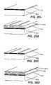
- FIG. 20 dthe cavity has been modified to alter it's mechanical behavior.
- a stiffening layer, 510has been added to limit deformation of the membrane while in the driven state. This assures that the two mirrors will remain parallel as a driving voltage is gradually increased.
- the resulting devicecan be driven in analog mode (e.g., cavity 511 may be driven by 5 volts to achieve partial deformation of the cavity) so that continuous variation of its spectral characteristics may be achieved.
- FIG. 20Eillustrates an additional configuration.
- a stop layer 512has been added so that the position of the membrane 506 in the driven state may be a fixed offset from the wall 502 .
- Alternative optical, electrical, or mechanical responsesmay be accommodated in this fashion.
- the stop layermay act as an insulator between walls 506 and 502 , or its thickness may be set to achieve a certain center frequency when the device is driven.
- FIG. 20Fshows an encapsulated version of the device of the cavity.
- Encapsulation membrane 514is fabricated in the same fashion and using similar materials as the original cavity, 502 and 506 by use of the described processes. In this case, the process is used to build structures on top of an array of cavities which have already been fabricated.
- Encapsulation membrane 514is a continuous structure designed to be rigid and inflexible. The function of this encapsulation is multifold. First it acts as a hermetic seal so that the entire array can be purged with an inert gas and maintained at an appropriate pressure. Second, the electrical and optical properties may also be useful in the overall operation of the array.
- a voltagemay be applied to encapsulation membrane 514 , and the resulting electrostatic forces between membranes 514 and 506 can alter the hysteresis of the underlying cavity in a useful fashion.
- the collapse and release thresholdscan be modified beyond what is dictated by the structure of the cavity itself.
- the electrostatic forcesmay also aid in releasing the membrane 502 from the collapsed state should it become stuck during the normal course of operation.
- the encapsulation membrane 514may also be incorporated into the overall optical design of the cavity, providing another element with which to achieve the desired optical responses.
- the exposed side of the encapsulation membrane 514can provide a surface upon which drive circuitry may be fabricated or mounted.
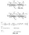
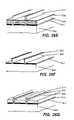
- the binary modulation modeis shown in FIG. 21A .
- incident light 512(the delta lambda represents a range of incident frequencies, e.g., the range of visible light) contains a spectral component which is at the resonant frequency of the device in the undriven state. Consequently this component (delta lambda n) is transmitted, 516 , and the remaining components (at nonresonant frequencies, delta lambda minus delta lambda n) are reflected, 514 .
- This operationis in the nature of the operation of a fabry-perot interference cavity.
- the resonant frequency of the deviceWhen the device is driven and the geometry altered to collapse (right side of figure), the resonant frequency of the device also changes. With the correct cavity dimensions, all of the incident light (delta lambda) is reflected.
- FIG. 21Ashows a binary mode of operation while FIG. 21B shows an analog mode, where a continuously variable voltage may be used to cause a continuously variable degree of translation of secondary mirror/conductor 506 .
- Thisprovides a mechanism for continuous frequency selection within an operational range because the resonant frequency of the cavity can be varied continuously.
- the transmitted wavelengthsare delta lambda n zero, while in the right hand side they are delta lambda n one.
- Equation 1defines the transmission T through a fabry-perot cavity.
- Ta, Tb, Ra, Rbare the transmittances and reflectances of the primary (a) and secondary (b) mirrors.
- Phi a and Phi bare the phase changes upon reflectance at the primary and secondary mirrors, respectively.
- Deltais the phase thickness.
- Equation 2defines the phase thickness in terms of the cavity spacing ds, the index of refraction of the spacer ns, and the angle of incidence, theta s.
- Equation 3shows that the transmission T becomes the transmission of the second mirror when the transmission of the first mirror approaches 0.
- FIGS. 22A through 22Fillustrate some of the possibilities and relate to the equations of FIG. 21B .
- T/Rtransmission and reflectivity
- the different modesare achieved by using different combinations of mirrors and cavity spacings. They are idealized in the sense that only approximations to these responses can be achieved in actual designs, with differences ranging from extraneous sidelobes to higher losses. Differences can be tolerated as long as the overall spectral response results in the perception of the desired color.
- the spectral characteristics of the mirrors usedcan be referred to as broad-band and narrow-band.
- the mirrorsare optimized for the visible range with a broad band mirror operating across the entire visible range (i.e., reflecting over a minimum range of 400 nm to 700 nm).
- a broad band mirroroperating across the entire visible range (i.e., reflecting over a minimum range of 400 nm to 700 nm).
- Such a mirroris denoted in the stack formula 1.671
- a narrow-band filter optimized for the color greenwould reflect only over the range of 500 nm to 570 nm, and transmit everywhere else.
- Such a filteris described by the stack formula 1
- the cavity spacing(i.e., cavity height) in both driven and undriven states can be set to a predetermined value by the film thicknesses used in its construction. These two values determine whether a cavity is resonant or non-resonant. For a resonant cavity, the spacing is determined such that the undriven state coincides with the resonant peak of the narrower of the two mirrors. When a device is non-resonant, it must be driven in order for the device to become resonant.
- FIG. 22Ashows a T/R plot of a cavity having broad band mirrors on both layers of the cavity.
- thisresults in transmission/reflection peaks which occur at wavelengths which are approximately integral multiples of the cavity spacing.
- the notation m delta lambda n in FIG. 21Adenotes the fact that there may be a series of peaks.
- Thisis classic fabry-perot behavior.
- the driven stateshown to the right in FIG. 22A
- the cavity resonanceis shifted out of the visible range causing the device to act like a broadband mirror.
- FIG. 22Bshows a T/R plot for a cavity having one broad band and one narrow band mirror.
- This devicehas a resonant cavity, causing a transmission peak at the center of the narrow-band mirror's passband when the device is in the undriven state.
- Driving the device(right hand side of FIG. 22B ) shifts the cavity resonance away from that of the narrow band mirror, and the device acts like a broadband mirror.
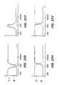
- the cavityis like that of FIG. 22B , except the cavity is non-resonant which results in broadband mirror cavity behavior in the undriven state.
- the cavity spacingshifts into resonance, causing a transmission peak centered on the narrow-band mirror.
- FIG. 22Dshows the performance of a resonant cavity with two narrow-band mirrors. When undriven, there is a transmission peak centered on the mirrors' response. Since the mirrors are narrow-band, the overall cavity response is that of a broad-band transmitter.
- Driving the device out of resonanceresults in a reflective peak at the narrow-band center frequency.
- the cavity of FIG. 22Ehas two narrow band mirrors, but it is a non-resonant cavity. Consequently its behavior is opposite that of the cavity portrayed in FIG. 22D .
- the transmissionapproaches zero for frequencies outside its range. This is essentially the transmission of mirror b.
- the transmissionbecomes a maximum outside the frequency range. In either case, the spurious peaks typical of a fabry-perot are avoided. The result is a device which can be described as a single mode resonant cavity.
- both of the mirrorsare narrow banded, then fabry-perot type behavior occurs only when the cavity spacing is correct. Making the mirrors narrow enough allows only a single peak to occur. Then it is unnecessary to be concerned about spurious peaks that might occur within the visible range.
- FIG. 22Fis for a cavity with a simpler design involving only a metallic mirror on one wall and a hybrid filter on the other wall.
- the hybrid filteris a combination of a narrow bandpass filter (outer surface) and an induced absorber (inner surface).
- the induced absorberis a simple structure which can consist of one or more dielectric or dielectric and metallic films. The function of the absorber is to cause incident light of a specified frequency range to be absorbed by a reflective surface (i.e. mirror).
- the induced absorberonly functions when it is in contact with the mirror, otherwise it is inconsequential.
- the hybrid filter(a green centered narrow bandpass/induced absorber) reflects everything but the green light, which is unaffected by the induced absorber and subsequently reflected by the metallic mirror.
- the overall cavity responseis like that of a broad-band mirror.
- the hybrid filtercomes into contact with the metallic mirror.
- the absorbercouples the green light into the mirror, and the result is an absorption peak at that wavelength.
- FIGS. 22G through 22 AFillustrate additional idealized optical responses useful in fabricating a full color or monochrome display. Specifically, FIGS. 22G through 22N portray broadband responses covering the entire visible range. These would be useful in creating a black and white display or a color display if they were used in conjunction with an external color filter mechanism.
- the responses shown in FIGS. 220 through 22Tact on 1 ⁇ 3 of the visible spectrum.
- FIGS. 22 U through 22 AFare representative of responses which act on 2 ⁇ 3 of the visible spectrum. For example, FIGS.
- FIGS. 22 AC and 22 ADillustrate a response where the crossover has blue on one side and green/red on the other while FIGS. 22W and 22X have red on one side and green/blue on the other.
- the responses illustrated in FIGS. 22 G through 22 AFcould be combined in pairs to produce two state modulators, some of which are shown in FIGS. 22B through 22F .
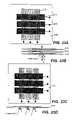
- a red 3 ⁇ 3 pixel (i.e., 9 cavities) subtractive mode display array based on the cavity device using the N-N (narrow band-narrow band) configuration of FIG. 22Dis shown.
- the cavity pixelsare formed at the intersections of primary mirror/conductors 602 and secondary mirror/conductors 604 .
- the displayis fabricated on substrate 608 and driven via contact pads 606 connected to each conductor/mirror 604 .
- a full nine-pixel displaycomprises three replications of the array of FIG. 23A arranged on top of one another and fabricated on separate substrates or color planes 610 , 612 , 614 , as shown in FIG. 23B .
- Each of the individual color planesinteracts only with and reflects one color (e.g., red, green, or blue), while passing all other colors. This is done by selecting the mirror spectral characteristic and cavity spacing in each color plane appropriately.
- the color planesare physically aligned and electrically driven through the contact pads to produce full color images. The image would be viewed from below in FIG. 23B .
- a display configurationutilizes both binary and analog versions of the cavity.
- this schemethere is a binary array which has been designed to modulate across the entire visible spectrum; it is either black or white.
- Using the binary array to perform brightness control and the analog array to perform color selectionallows for the generation of images which have a color gamut that is infinitely variable. This approach would make possible more accurate representations of imagery than are currently possible with fixed color filters such as phosphors or dyes.
- Pixel size and overall display sizecan be altered to make the displays useful in many different display and spatial light modulator applications. These include direct view and projection displays, optical computing, holographic memory, and any other situation where a one or two dimensional modulator of light can be used.
- the secondary mirror/conductorexperiences a displacement towards the substrate until the force of restoration balances the electrical attraction.
- the force of restorationis completely overcome and the membrane is pressed tightly against the substrate.
- the voltagecan then be lowered again to some degree without affecting the position of the membrane. Only if the voltage is then lowered significantly or eliminated will the membrane be released. Because the membrane is under tensile stress, it will then pull itself away from the substrate when the voltage is released. This hysteresis can be used to achieve matrix addressing of a two-dimensional array, as explained with reference to FIG. 24B .
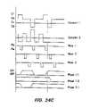
- the displaycan be addressed and brightness controlled using control pulse sequences in the driving voltage. Shown is a timing diagram for a 3 ⁇ 3 pixel array analogous to that shown in FIG. 23A .
- a continuous series of ⁇ 5 volts scanning pulsesis applied to the rows (rows 1–3) of the pixel array in a sequential fashion, as seen in the charts labelled “Row”.
- the pulsesappear at the same frequency on each of the rows but the pulses for different rows are staggered. These pulses are insufficient in their own right to cause the membrane to collapse.
- the columns (cols. 1–3) of the pixel arrayare maintained at a bias voltage of 5 volts so that the nominal voltage across each unactivated pixel is 5 volts.
- the nominal row and column potentialsare 5 and ⁇ 5 volts respectively, resulting in a cavity voltage of 10 volts.
- the total voltage across the cavitybecomes 15 volts which is sufficient to drive the secondary mirror/conductor into the collapsed state, where it will remain until the end of the scan when all of the column voltages are pulsed to zero.
- the three charts at the bottom of FIG. 24Bshow the on and off states of the three pixels identified there by row and column numbers.
- the intensity or brightness of a pixelmay be varied by changing the fraction of the scan during which the pixel is activated.
- the scan cyclebegins at 198 and ends at 199 .
- the frequency of the scan pulsesis such that six pulses of a given row fall within the scan cycle, providing an opportunity to activate a pixel at any one of six times during each cycle. Once the pixel is activated it stays on until the end of the cycle. Therefore six different intensities are possible for each pixel.
- pixel C 1 R 1is at full brightness
- pixel C 2 R 2is at 4/6 brightness
- pixel C 3 R 2is at 1 ⁇ 6 brightness. All pixels are cleared at the end of the scan and the cycle begins again. Since these structures can be driven at frequencies as high as 50 kHz, this method of brightness control is practical. Assuming six brightness levels, there would be a possibility of more than 8 thousand row scans per second.
- FIG. 24CShown in FIG. 24C is an addressing scheme based on voltages derived from the hysteresis curve illustrated in FIG. 24D . Like the previous scheme a series of scanning pulses is applied sequentially to the rows. When the column is sitting at the bias voltage of
- C bV 1
- the total row/column voltage when the scanning pulse is appliedis C b ⁇ R s ⁇ V 1 +1 ⁇ 2(V 2 ⁇ V 1 ).
- the diagram of FIG. 24Dshows that this is insufficient to move a pixel from the on state to the off state or from the off state to the on state.
- Addressingcan be accomplished by breaking the maximum on time (i.e., maximum brightness) into eight different segments. Each segment represents a bit ranging from most significant to least significant in an 8 bit word. The least significant bit is the smallest in length, equal to 1/256 of the maximum time, while the next most significant is twice that length. Each subsequent bit is doubled in length until the most significant bit. In this fashion, a single row only has to be addressed a total of eight times (for eight bits of gray scale) to create arbitrary values of brightness for a given pixel, thus significantly reducing the required number of row scans.
- substrate 700is first cleaned using standard procedures.
- the substratemay be of many different materials including silicon, plastic, mylar, or quartz.
- the primary requirementis that the material be able to support an optically smooth, though not necessarily flat, finish.
- a preferred materialwould likely be glass, which would permit both transmissive and reflective operation in the visible range.
- a photoresist 704has been patterned on the primary conductor/mirror.
- the photoresistmay be of a positive or negative type.
- the standard procedure for this stepinvolves spinning of the resist, softbaking at 90 C, exposing through an appropriate mask, developing to produce the pattern, and hardbaking at 130 C.
- the photoresist patternis defined in the primary conductor/mirror by an etching process.
- This stepcan be achieved either by wet chemical means or by plasma or reactive ion etching (RIE).
- RIEreactive ion etching
- the choice of etching techniquedepends on the nature of the conductor/mirror. In the case of an aluminum conductor/mirror, chlorine gas may be used to perform the etch, with a standard chamber power of 100 watts producing an etch rate of 100 angstroms/min. Some mirror materials may resist RIE and in such cases a technique such as ion milling may be used. All RIE steps are performed at a pressure of 30 mtorr unless otherwise noted. All plasma etch steps are performed at a pressure of 100 mtorr unless otherwise noted. The photoresist is removed using standard solvents.
- the conductor/mirrormay be defined using the well-known procedure called lift-off. This procedure is used to define a layer in a subsequent step and is described below.
- support rail material 706has been deposited using one of the methods mentioned previously.
- This materialshould be an insulator, for example silicon dioxide or silicon nitride.
- the materialshould be deposited uniformly, and at a thickness equal to thickness of the spacer layer, which will be deposited later. This thickness should in general be at least a multiple of the wavelength of light of interest. A thickness of 0.5 microns would place such a device near the middle of the visible spectrum.
- photoresist layer 708is spun on and hardbaked. Since this layer will not be photolithographically defined, other polymeric materials may be used instead. The only requirement is that they dissolve in solvents such as acetone or methanol, and be able to withstand a vacuum. This is the first step in defining a lift-off stencil.
- template layer 710has been deposited using one of the methods of PVD.
- the layeris of silicon dioxide though other materials are possible. Ideally the material should be etched using a process which does not affect the underlying resist.
- Buffered Oxide Etch (BOE)which consists of Hydrofluoric acid diluted 7:1 with water can perform this step in 15 seconds.
- the layerneed only be a thousand angstroms thick.
- photoresist layer 712has been spun-on and patterned in a manner already discussed.
- the pattern of resist layer 711has been transferred to layers 710 and 708 .
- the BOEis used to etch through the silicon dioxide layer 710 .
- An oxygen plasmais used to etch through resist layer 708 , and to remove resist layer 711 .
- Plasma etchingdiffers from RIE in that it tends to be less anisotropic, yielding profiles that are not purely vertical.
- resist layer 708has been slightly underetched in order to facilitate removal of the lift-off stencil.
- RIEusing a carbon tetrafluoride chemistry (CF4/O2 6:4) is then applied to etching through layer 706 .
- spacer layer 712is deposited using PVD techniques.
- This materialcan be any number of different compounds which can be deposited using this technique. There are two key requirements for such a material. The first is that the material be soluble in water or chemically removed by a liquid etchant other than solvents such as acetone or methanol which will be required to remove the lift-off stencil.
- a liquid etchantother than solvents such as acetone or methanol which will be required to remove the lift-off stencil.
- An example of such an etchantwould be water and appropriate materials include lithium fluoride, aluminum fluoride, and sodium chloride.
- the secondis that it be deposited with extreme uniformity and thickness control.
- the formerallows resulting structures to be underetched without damage by using water as the final etchant.
- Wateris an extremely benign solvent, and makes possible the incorporation of many different mirror, conductor, and structural materials in the final device.
- the spacermay also be composed of a polymeric material such as hardbaked photoresist or polyimide.
- a technique other than spinningmust be used to deposit the polymer. Two such techniques include extrusion and capillary coating. The consequence of using such a spacer is that all subsequent process steps must be low temperature in nature to prevent outgassing and shrinkage of this layer. In this case, the spacer is ultimately removed using an oxygen plasma.
- diamineis one example of such a material.
- the required uniformitycould be obtained and the spacer layer again removed using an oxygen based plasma.
- the use of different plasma chemistrieswould also permit etching of inorganic spacers as well. Chlorinated plasmas for example could be used to remove an aluminum spacer.
- the stencilis subsequently removed using an ultrasonic acetone bath and methanol rinse or other polymer dissolving solvent. This also removes or lifts off excess deposited spacer material and is what constitutes the final step of the lift-off process.
- An oxygen plasmamay also be used to accomplish this step though the material which has been lifted off must be removed. This can be done using a high pressure gas jet.
- a natural overhangmay be produced via overexposure.
- positive photoresistusing a technique known as image-reversal. This would preclude the need to put down a sacrificial photoresist layer and a subsequent SiO2 layer.
- secondary conductor/mirror layer(s) and support membrane ( 714 )are deposited.
- the nature of the conductor/mirroris dependent on the application.
- the support membranemust have a tensile residual stress. Tensile stress is required for two reasons. First so that the resulting membranes will be flat and therefore parallel to the substrate in the quiescent state. Secondly, such structures have a tendency to stick when the membranes come in contact with the substrate. Sufficient tensile stress is required pull the membrane away when the drive voltage is reduced.
- the membranemust have the appropriate optical characteristics as well. For visible light this would mean transparency in the visible region. Silicon nitride is one candidate for this role for it can be deposited using plasma enhanced chemical vapor deposition (PECVD) with controlled stress. Other candidates include titanium dioxide, magnesium fluoride and calcium fluoride, all of which can be deposited using e-beam evaporation with a resulting tensile stress.
- PECVDplasma enhanced chemical vapor deposition
- photoresist layer 716has been spun-on and patterned in a manner discussed above.
- layer(s) 714have been etched according to the pattern of resist layer 716 .
- the final etchis accomplished by placing the device in water for a period of time.
- the wateris agitated, and when the devices are fully etched they are dried.
- One variation on this stepinvolves the use of t-butyl alcohol to displace the water when the etch is finished.
- the devicesare then placed in a chamber at approximately 32 degrees centigrade to cause the alcohol to freeze. After this step the devices are placed into a vacuum chamber where the air is then evacuated. This causes the alcohol to sublime and can reduce membrane sticking during the drying phase.
- FIGS. 26A through 26CAnother alternative process has initial steps of assembly shown in FIGS. 26A through 26C , analogous to those shown in FIGS. 25A through 25C .
- photoresist or polymer layer 806is spun on and a stencil layer, 208 , of silicon dioxide is deposited using PVD. This layer must be thicker than the spacer layer to be deposited.
- resist layer 810has been spun-on and patterned using standard procedures.
- this stepuses BOE and an oxygen plasma etch to define a lift-off stencil.
- the spacer materialis chosen and deposited as described in FIG. 25J .
- the stencilis subsequently removed using an ultrasonic acetone bath and methanol rinse.
- the step shown in FIG. 26Iis analogous to that shown in FIG. 25K .
- photoresist layer 814has been spun-on and patterned.
- layer(s) 812have been etched according to the pattern of resist layer 214 .
- the final etchis accomplished in a manner described above.
- All of the materials used for the mirrorsmust be deposited in such a way that their stress can be controlled. Ideally, they are deposited as “stress balanced” which means that the overall stress of the film or film stack is zero. Since the ultimate goal is that the support membrane conductor/mirror combination have an overall tensile stress, conductor/mirror films with compressive stress may be accommodated by having a high stress support membrane.
- IADion assisted deposition
- the residual stress of almost any film of interestmay be controlled by bombarding the substrate with an independently controlled stream of neutral ions during the deposition process. This make possible the total mechanical decoupling of the support material from the optical material. As a result, emphasis can be placed on depositing an optically neutral support membrane with ideal mechanical characteristics. In the same manner, a “mechanically neutral” (i.e. stressless) conductor/mirror can be deposited with ideal optical characteristic.
- the simplest conductor/mirror configuration for an individual cavityis formed from a layer 900 that is either the substrate for the primary conductor/mirror, or the support membrane if this is the secondary.
- Layer 902is a metallic film with a thickness on the order of several hundred angstroms. The film can be of aluminum, silver, or any number of metals, based on the spectral, and resistive properties as well as the ease with which the metal can be etched.
- Layer 904is an insulator and/or reflection enhancement film. This can be formed by oxidizing the metal, if aluminum is being used, in an oxygen plasma thus forming a thin layer of aluminum oxide. Alternatively, insulating layers or reflection enhancement layers may be deposited in a manner discussed before.
- Metallic mirrorsmust be somewhat transmissive and therefore no more than several hundred angstroms thick. Insulator films can have thicknesses from one hundred to several thousand angstroms. Their thickness is determined by the kind of voltages expected in driving the devices.
- the conductor 906is either a transparent film such as indium tin oxide (ITO), or a very thin metallic layer such as gold. Either can be deposited using suitable film deposition methods. Thicknesses for the ITO should be in the range of several thousand angstroms, and metallic conductors less than 100 angstroms.
- 908is a multilayer dielectric stack comprising the mirror. Such a mirror consists of alternating dielectric films with differing indexes of refraction deposited by a suitable PVD process. By choosing films with appropriate thicknesses and indexes, mirrors with tailorable spectral characteristics can be fabricated as is well known in the art. In general, the thickness of the individual layers is one quarter the wavelength of the light of interest.
- these mirrorsmay be deposited using a technique known as codeposition.
- codepositionIn this case, PVD is used to deposit two materials with different refractive indices simultaneously. Using computer control the refractive index of the resulting film can be varied continuously between those of either film. This deposition technique makes possible mirrors with virtually any spectral characteristic.
- a dielectric mirror 908is deposited directly on substrate 900 .
- Metallic conductor 902 and insulator 904are deposited and patterned such that they form a border around the periphery of the mirror. Using this configuration, it is possible to provide drive voltages to the devices without compromising throughput since the conductor can be placed outside the active area of the device.
- FIG. 27Dshows a planar view of this mirror configuration.
- a linear tunable filteris shown which has been fabricated using the process sequence defined above.
- the major differenceis the nature of the mask used to define the self-supporting membrane, which is comprised of support 1006 and 1008 .
- the substrate, 1000is transparent in thee frequency region of interest, and electrodes 1004 are used to drive the device.
- Dielectric mirror 1002are defined separately to produce a configuration like that of FIGS. 27 c , 27 d .
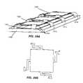
- Three filtersare shown though many more can be fabricated. Each filter 1010 , 1012 , and 1014 is driven independently so that individual frequencies may be separated from an incident light beam.
- FIG. 28 bis a top view of the structure.
- a device known as a deformable mirrorincludes a self-supporting membrane 1102 fabricated on a substrate 1100 .
- a potentialis applied between actuator electrodes 1104 and conducting mirror 1106 , the surface of the mirror can be deformed in a controllable manner.
- Such a devicecan be used as a component in an adaptive optics system, or in any situation where control of an incident wavefront is required.
Landscapes
- Physics & Mathematics (AREA)
- Engineering & Computer Science (AREA)
- General Physics & Mathematics (AREA)
- Optics & Photonics (AREA)
- Computer Hardware Design (AREA)
- Theoretical Computer Science (AREA)
- Nonlinear Science (AREA)
- Chemical & Material Sciences (AREA)
- Nanotechnology (AREA)
- Spectroscopy & Molecular Physics (AREA)
- Life Sciences & Earth Sciences (AREA)
- Biophysics (AREA)
- Crystallography & Structural Chemistry (AREA)
- Mechanical Light Control Or Optical Switches (AREA)
Abstract
Description
whereE (overbar) is the complex amplitude of the electric field of the sum of the transmitted wave and the reflected wave;E0is the complex amplitude of the electric field of the transmitted20 wave;Er, is the complex amplitude of the electric field of the reflective wave; x(hat) is the orientation of the electric field of the wave;H is the amplitude of the magnetic field; y(hat) is the orientation of the magnetic field; μo is the permeability of free space; ∈0is the permittivity of free space; k=ωsqrt[μ0∈0] is the wavenumber; and η=sqrt[μ0/∈0] is the impedance of free space. For z>0 (i.e., within free space) only the transmitted wave exists and is represented by
E (overbar) is the complex amplitude the transmitted wave at z=0, kt=sqrt[μ∈] is its wavenumber; η=sqrt[μ/∈] is the impedance of the medium, i.e. z>0. Boundary conditions (z=0) for tangential electric fields are imposed on
{circumflex over (x)}[E0+Er]={circumflex over (x)}Et (5)
In the same way, continuity for tangential magnetic fields (z=0) at the boundary yields,
- Dividing
equations 5 and 6 byE0, andE0/η0respectively gives the following two equations:
ŷ(1/η0)(E0−ER)={circumflex over (y)}(1/ηt)Et (6)
1+Er/E0=Et/E0 (7)
1−ER/E0=(η0/ηt) (Et/E0) (8)
Er/E0is called r and is the complex reflection coefficient whileEt/η0=T is called the complex transmission coefficient, and ηt/η0=ηnis the normalized wave impedance. Solving for T and Γ yields
- Dividing
For matched impedance values, η0=ηn, the reflection coefficient is zero, and T=1 (i.e., no reflection), and in the case of a load at the boundary, a matched antenna, there is complete absorption.
I′=jωq (11)
{overscore (J)}({overscore (r)}′)={circumflex over (z)}Idδ({overscore (r)}′) (12)
whereqis the charge density; z(hat) indicates the direction of the current (along the z-axis); ω is angular frequency; and d is the distance between ideal point charges representing the dipole. The vector potential A(overbar) in polar coordinates is given by
where θ represents the angle relative to the dipole; θ (hat) is the angular orientation of the wave; μ0is the permeability of free space; r is radius from the dipole; r(hat) is radial orientation of the wave; Aris the radial component of the vector potential; Aθ is the angular component of the vector potential; and k is a factor which is used to represent sinusoidally varying waves. The H field is given by
where φ is elevation, with respect to the dipole. The E field is given by, The far-field equation is given by
V(z)=V+e−jkz+ΓLejkz (17)
Because zL=z0, ΓL=0, and equation 17 simplifies to
V(z)=V+e−jkz (18)
C1=V2and a scanning pulse is applied, the resulting difference is C1−Rs=V2+½(V2−V1). This is sufficient to turn a pixel on, however the voltage difference is not sufficient to turn pixels with a scan voltage of Rb=0 on. Conversely, the application of C0=−V1volts to the column during a scan pulse brings the total difference to V0=C0−R3=−V1+½(V2−V1) which is sufficient to turn a pixel off. In this fashion, pixels may be driven arbitrarily into one state or another, precluding the need for a reset pulse as is required in the previous approach.
Claims (20)
Priority Applications (14)
| Application Number | Priority Date | Filing Date | Title |
|---|---|---|---|
| US10/082,397US7126738B2 (en) | 1995-05-01 | 2002-02-25 | Visible spectrum modulator arrays |
| US11/267,939US8014059B2 (en) | 1994-05-05 | 2005-11-04 | System and method for charge control in a MEMS device |
| US11/267,819US7776631B2 (en) | 1994-05-05 | 2005-11-04 | MEMS device and method of forming a MEMS device |
| US11/585,791US7385748B2 (en) | 1995-05-01 | 2006-10-23 | Visible spectrum modulator arrays |
| US11/841,810US7738157B2 (en) | 1994-05-05 | 2007-08-20 | System and method for a MEMS device |
| US11/841,847US7848004B2 (en) | 1994-05-05 | 2007-08-20 | System and method for a MEMS device |
| US11/841,820US7852545B2 (en) | 1994-05-05 | 2007-08-20 | Method and device for modulating light |
| US11/841,833US7800809B2 (en) | 1994-05-05 | 2007-08-20 | System and method for a MEMS device |
| US11/841,780US7808694B2 (en) | 1994-05-05 | 2007-08-20 | Method and device for modulating light |
| US11/841,795US8081369B2 (en) | 1994-05-05 | 2007-08-20 | System and method for a MEMS device |
| US11/841,726US7839556B2 (en) | 1994-05-05 | 2007-08-20 | Method and device for modulating light |
| US12/813,286US7929197B2 (en) | 1996-11-05 | 2010-06-10 | System and method for a MEMS device |
| US12/939,087US20110043891A1 (en) | 1994-05-05 | 2010-11-03 | Method for modulating light |
| US13/225,357US20120062310A1 (en) | 1994-05-05 | 2011-09-02 | System and method for charge control in a mems device |
Applications Claiming Priority (5)
| Application Number | Priority Date | Filing Date | Title |
|---|---|---|---|
| PCT/US1995/005358WO1995030924A1 (en) | 1994-05-05 | 1995-05-01 | Visible spectrum modulator arrays |
| US08/744,253US5986796A (en) | 1993-03-17 | 1996-11-05 | Visible spectrum modulator arrays |
| US09/378,143US20010003487A1 (en) | 1996-11-05 | 1999-08-20 | Visible spectrum modulator arrays |
| US09/413,222US7123216B1 (en) | 1994-05-05 | 1999-10-05 | Photonic MEMS and structures |
| US10/082,397US7126738B2 (en) | 1995-05-01 | 2002-02-25 | Visible spectrum modulator arrays |
Related Parent Applications (2)
| Application Number | Title | Priority Date | Filing Date |
|---|---|---|---|
| US09/378,143DivisionUS20010003487A1 (en) | 1994-05-05 | 1999-08-20 | Visible spectrum modulator arrays |
| US09/413,222ContinuationUS7123216B1 (en) | 1994-05-05 | 1999-10-05 | Photonic MEMS and structures |
Related Child Applications (5)
| Application Number | Title | Priority Date | Filing Date |
|---|---|---|---|
| US11/267,819Continuation-In-PartUS7776631B2 (en) | 1994-05-05 | 2005-11-04 | MEMS device and method of forming a MEMS device |
| US11/267,939Continuation-In-PartUS8014059B2 (en) | 1994-05-05 | 2005-11-04 | System and method for charge control in a MEMS device |
| US11/585,791ContinuationUS7385748B2 (en) | 1994-05-05 | 2006-10-23 | Visible spectrum modulator arrays |
| US11/585,791Continuation-In-PartUS7385748B2 (en) | 1994-05-05 | 2006-10-23 | Visible spectrum modulator arrays |
| US11/841,726Continuation-In-PartUS7839556B2 (en) | 1994-05-05 | 2007-08-20 | Method and device for modulating light |
Publications (4)
| Publication Number | Publication Date |
|---|---|
| US20030072070A1 US20030072070A1 (en) | 2003-04-17 |
| US20050213183A9 US20050213183A9 (en) | 2005-09-29 |
| US20060139723A9 US20060139723A9 (en) | 2006-06-29 |
| US7126738B2true US7126738B2 (en) | 2006-10-24 |
Family
ID=24992040
Family Applications (3)
| Application Number | Title | Priority Date | Filing Date |
|---|---|---|---|
| US09/378,143AbandonedUS20010003487A1 (en) | 1994-05-05 | 1999-08-20 | Visible spectrum modulator arrays |
| US10/082,397Expired - Fee RelatedUS7126738B2 (en) | 1994-05-05 | 2002-02-25 | Visible spectrum modulator arrays |
| US11/585,791Expired - Fee RelatedUS7385748B2 (en) | 1994-05-05 | 2006-10-23 | Visible spectrum modulator arrays |
Family Applications Before (1)
| Application Number | Title | Priority Date | Filing Date |
|---|---|---|---|
| US09/378,143AbandonedUS20010003487A1 (en) | 1994-05-05 | 1999-08-20 | Visible spectrum modulator arrays |
Family Applications After (1)
| Application Number | Title | Priority Date | Filing Date |
|---|---|---|---|
| US11/585,791Expired - Fee RelatedUS7385748B2 (en) | 1994-05-05 | 2006-10-23 | Visible spectrum modulator arrays |
Country Status (1)
| Country | Link |
|---|---|
| US (3) | US20010003487A1 (en) |
Cited By (125)
| Publication number | Priority date | Publication date | Assignee | Title |
|---|---|---|---|---|
| US20060077125A1 (en)* | 2004-09-27 | 2006-04-13 | Idc, Llc. A Delaware Limited Liability Company | Method and device for generating white in an interferometric modulator display |
| US20060077124A1 (en)* | 2004-09-27 | 2006-04-13 | Gally Brian J | Method and device for manipulating color in a display |
| US20060262126A1 (en)* | 1999-10-05 | 2006-11-23 | Idc, Llc A Delaware Limited Liability Company | Transparent thin films |
| US20060274398A1 (en)* | 2005-06-03 | 2006-12-07 | Chen-Jean Chou | Interferometric modulator with internal polarization and drive method |
| US7403180B1 (en) | 2007-01-29 | 2008-07-22 | Qualcomm Mems Technologies, Inc. | Hybrid color synthesis for multistate reflective modulator displays |
| US7405852B2 (en) | 2005-02-23 | 2008-07-29 | Pixtronix, Inc. | Display apparatus and methods for manufacture thereof |
| US20080225370A1 (en)* | 2007-03-16 | 2008-09-18 | Active Optical Systems, Llc | Low-cost continuous phase sheet deformable mirror |
| US20080288225A1 (en)* | 2007-05-18 | 2008-11-20 | Kostadin Djordjev | Interferometric modulator displays with reduced color sensitivity |
| US7460291B2 (en) | 1994-05-05 | 2008-12-02 | Idc, Llc | Separable modulator |
| US20080316566A1 (en)* | 2007-06-19 | 2008-12-25 | Qualcomm Incorporated | High aperture-ratio top-reflective am-imod displays |
| US7492503B2 (en) | 2004-09-27 | 2009-02-17 | Idc, Llc | System and method for multi-level brightness in interferometric modulation |
| US7515327B2 (en) | 2004-09-27 | 2009-04-07 | Idc, Llc | Method and device for corner interferometric modulation |
| US7542198B2 (en) | 2004-09-27 | 2009-06-02 | Idc, Llc | Device having a conductive light absorbing mask and method for fabricating same |
| US7551344B2 (en) | 2005-02-23 | 2009-06-23 | Pixtronix, Inc. | Methods for manufacturing displays |
| US7553684B2 (en)* | 2004-09-27 | 2009-06-30 | Idc, Llc | Method of fabricating interferometric devices using lift-off processing techniques |
| US7561323B2 (en) | 2004-09-27 | 2009-07-14 | Idc, Llc | Optical films for directing light towards active areas of displays |
| US7612932B2 (en) | 2004-09-27 | 2009-11-03 | Idc, Llc | Microelectromechanical device with optical function separated from mechanical and electrical function |
| US7612933B2 (en) | 2008-03-27 | 2009-11-03 | Qualcomm Mems Technologies, Inc. | Microelectromechanical device with spacing layer |
| US7630121B2 (en) | 2007-07-02 | 2009-12-08 | Qualcomm Mems Technologies, Inc. | Electromechanical device with optical function separated from mechanical and electrical function |
| US7629197B2 (en) | 2006-10-18 | 2009-12-08 | Qualcomm Mems Technologies, Inc. | Spatial light modulator |
| US7636189B2 (en) | 2005-02-23 | 2009-12-22 | Pixtronix, Inc. | Display methods and apparatus |
| US20090323154A1 (en)* | 2008-06-25 | 2009-12-31 | Qualcomm Mems Technologies, Inc. | Backlight displays |
| US7643202B2 (en) | 2007-05-09 | 2010-01-05 | Qualcomm Mems Technologies, Inc. | Microelectromechanical system having a dielectric movable membrane and a mirror |
| US7663794B2 (en) | 2004-09-27 | 2010-02-16 | Qualcomm Mems Technologies, Inc. | Methods and devices for inhibiting tilting of a movable element in a MEMS device |
| US7704772B2 (en) | 2004-05-04 | 2010-04-27 | Qualcomm Mems Technologies, Inc. | Method of manufacture for microelectromechanical devices |
| US7710632B2 (en) | 2004-09-27 | 2010-05-04 | Qualcomm Mems Technologies, Inc. | Display device having an array of spatial light modulators with integrated color filters |
| US7715085B2 (en) | 2007-05-09 | 2010-05-11 | Qualcomm Mems Technologies, Inc. | Electromechanical system having a dielectric movable membrane and a mirror |
| US7715079B2 (en) | 2007-12-07 | 2010-05-11 | Qualcomm Mems Technologies, Inc. | MEMS devices requiring no mechanical support |
| US7719747B2 (en) | 2004-09-27 | 2010-05-18 | Qualcomm Mems Technologies, Inc. | Method and post structures for interferometric modulation |
| US7742220B2 (en) | 2007-03-28 | 2010-06-22 | Qualcomm Mems Technologies, Inc. | Microelectromechanical device and method utilizing conducting layers separated by stops |
| US7746529B2 (en) | 2005-02-23 | 2010-06-29 | Pixtronix, Inc. | MEMS display apparatus |
| US7746539B2 (en) | 2008-06-25 | 2010-06-29 | Qualcomm Mems Technologies, Inc. | Method for packing a display device and the device obtained thereof |
| US7768690B2 (en) | 2008-06-25 | 2010-08-03 | Qualcomm Mems Technologies, Inc. | Backlight displays |
| US7773286B2 (en) | 2007-09-14 | 2010-08-10 | Qualcomm Mems Technologies, Inc. | Periodic dimple array |
| US7782517B2 (en) | 2007-06-21 | 2010-08-24 | Qualcomm Mems Technologies, Inc. | Infrared and dual mode displays |
| US7807488B2 (en) | 2004-09-27 | 2010-10-05 | Qualcomm Mems Technologies, Inc. | Display element having filter material diffused in a substrate of the display element |
| US7808695B2 (en) | 2006-06-15 | 2010-10-05 | Qualcomm Mems Technologies, Inc. | Method and apparatus for low range bit depth enhancement for MEMS display architectures |
| US7808694B2 (en) | 1994-05-05 | 2010-10-05 | Qualcomm Mems Technologies, Inc. | Method and device for modulating light |
| US7830588B2 (en) | 1996-12-19 | 2010-11-09 | Qualcomm Mems Technologies, Inc. | Method of making a light modulating display device and associated transistor circuitry and structures thereof |
| US7839557B2 (en) | 2004-09-27 | 2010-11-23 | Qualcomm Mems Technologies, Inc. | Method and device for multistate interferometric light modulation |
| US7847999B2 (en) | 2007-09-14 | 2010-12-07 | Qualcomm Mems Technologies, Inc. | Interferometric modulator display devices |
| US7852545B2 (en) | 1994-05-05 | 2010-12-14 | Qualcomm Mems Technologies, Inc. | Method and device for modulating light |
| US7852546B2 (en) | 2007-10-19 | 2010-12-14 | Pixtronix, Inc. | Spacers for maintaining display apparatus alignment |
| US7855824B2 (en) | 2004-03-06 | 2010-12-21 | Qualcomm Mems Technologies, Inc. | Method and system for color optimization in a display |
| US7855826B2 (en) | 2008-08-12 | 2010-12-21 | Qualcomm Mems Technologies, Inc. | Method and apparatus to reduce or eliminate stiction and image retention in interferometric modulator devices |
| US7859740B2 (en) | 2008-07-11 | 2010-12-28 | Qualcomm Mems Technologies, Inc. | Stiction mitigation with integrated mech micro-cantilevers through vertical stress gradient control |
| US7872792B2 (en) | 1998-04-08 | 2011-01-18 | Qualcomm Mems Technologies, Inc. | Method and device for modulating light with multiple electrodes |
| US7876489B2 (en) | 2006-06-05 | 2011-01-25 | Pixtronix, Inc. | Display apparatus with optical cavities |
| US7898723B2 (en) | 2008-04-02 | 2011-03-01 | Qualcomm Mems Technologies, Inc. | Microelectromechanical systems display element with photovoltaic structure |
| US7898521B2 (en) | 2004-09-27 | 2011-03-01 | Qualcomm Mems Technologies, Inc. | Device and method for wavelength filtering |
| US7907319B2 (en) | 1995-11-06 | 2011-03-15 | Qualcomm Mems Technologies, Inc. | Method and device for modulating light with optical compensation |
| US7911428B2 (en) | 2004-09-27 | 2011-03-22 | Qualcomm Mems Technologies, Inc. | Method and device for manipulating color in a display |
| US7916378B2 (en) | 2007-03-08 | 2011-03-29 | Qualcomm Mems Technologies, Inc. | Method and apparatus for providing a light absorbing mask in an interferometric modulator display |
| US7924494B2 (en) | 2004-09-27 | 2011-04-12 | Qualcomm Mems Technologies, Inc. | Apparatus and method for reducing slippage between structures in an interferometric modulator |
| US7927654B2 (en) | 2005-02-23 | 2011-04-19 | Pixtronix, Inc. | Methods and apparatus for spatial light modulation |
| US7928928B2 (en) | 2004-09-27 | 2011-04-19 | Qualcomm Mems Technologies, Inc. | Apparatus and method for reducing perceived color shift |
| US7944599B2 (en) | 2004-09-27 | 2011-05-17 | Qualcomm Mems Technologies, Inc. | Electromechanical device with optical function separated from mechanical and electrical function |
| US7944604B2 (en) | 2008-03-07 | 2011-05-17 | Qualcomm Mems Technologies, Inc. | Interferometric modulator in transmission mode |
| US7952787B2 (en) | 2006-06-30 | 2011-05-31 | Qualcomm Mems Technologies, Inc. | Method of manufacturing MEMS devices providing air gap control |
| US20110148751A1 (en)* | 2004-09-27 | 2011-06-23 | Qualcomm Mems Technologies, Inc. | Method and device for manipulating color in a display |
| US7969638B2 (en) | 2008-04-10 | 2011-06-28 | Qualcomm Mems Technologies, Inc. | Device having thin black mask and method of fabricating the same |
| US7982700B2 (en) | 2004-09-27 | 2011-07-19 | Qualcomm Mems Technologies, Inc. | Conductive bus structure for interferometric modulator array |
| US7999993B2 (en) | 2004-09-27 | 2011-08-16 | Qualcomm Mems Technologies, Inc. | Reflective display device having viewable display on both sides |
| US8004743B2 (en) | 2006-04-21 | 2011-08-23 | Qualcomm Mems Technologies, Inc. | Method and apparatus for providing brightness control in an interferometric modulator (IMOD) display |
| US8004504B2 (en) | 2004-09-27 | 2011-08-23 | Qualcomm Mems Technologies, Inc. | Reduced capacitance display element |
| US8023167B2 (en) | 2008-06-25 | 2011-09-20 | Qualcomm Mems Technologies, Inc. | Backlight displays |
| US8040588B2 (en) | 2004-09-27 | 2011-10-18 | Qualcomm Mems Technologies, Inc. | System and method of illuminating interferometric modulators using backlighting |
| US8045252B2 (en) | 2004-02-03 | 2011-10-25 | Qualcomm Mems Technologies, Inc. | Spatial light modulator with integrated optical compensation structure |
| US8054527B2 (en) | 2007-10-23 | 2011-11-08 | Qualcomm Mems Technologies, Inc. | Adjustably transmissive MEMS-based devices |
| US8058549B2 (en) | 2007-10-19 | 2011-11-15 | Qualcomm Mems Technologies, Inc. | Photovoltaic devices with integrated color interferometric film stacks |
| US8061882B2 (en) | 2006-10-06 | 2011-11-22 | Qualcomm Mems Technologies, Inc. | Illumination device with built-in light coupler |
| US8072402B2 (en) | 2007-08-29 | 2011-12-06 | Qualcomm Mems Technologies, Inc. | Interferometric optical modulator with broadband reflection characteristics |
| US8081370B2 (en) | 2004-09-27 | 2011-12-20 | Qualcomm Mems Technologies, Inc. | Support structures for electromechanical systems and methods of fabricating the same |
| US8081373B2 (en) | 2007-07-31 | 2011-12-20 | Qualcomm Mems Technologies, Inc. | Devices and methods for enhancing color shift of interferometric modulators |
| US8098416B2 (en) | 2006-06-01 | 2012-01-17 | Qualcomm Mems Technologies, Inc. | Analog interferometric modulator device with electrostatic actuation and release |
| US8102407B2 (en) | 2004-09-27 | 2012-01-24 | Qualcomm Mems Technologies, Inc. | Method and device for manipulating color in a display |
| US8115987B2 (en) | 2007-02-01 | 2012-02-14 | Qualcomm Mems Technologies, Inc. | Modulating the intensity of light from an interferometric reflector |
| US8164821B2 (en) | 2008-02-22 | 2012-04-24 | Qualcomm Mems Technologies, Inc. | Microelectromechanical device with thermal expansion balancing layer or stiffening layer |
| US8193441B2 (en) | 2007-12-17 | 2012-06-05 | Qualcomm Mems Technologies, Inc. | Photovoltaics with interferometric ribbon masks |
| US8248560B2 (en) | 2008-04-18 | 2012-08-21 | Pixtronix, Inc. | Light guides and backlight systems incorporating prismatic structures and light redirectors |
| US8262274B2 (en) | 2006-10-20 | 2012-09-11 | Pitronix, Inc. | Light guides and backlight systems incorporating light redirectors at varying densities |
| US8270056B2 (en) | 2009-03-23 | 2012-09-18 | Qualcomm Mems Technologies, Inc. | Display device with openings between sub-pixels and method of making same |
| US8270062B2 (en) | 2009-09-17 | 2012-09-18 | Qualcomm Mems Technologies, Inc. | Display device with at least one movable stop element |
| US8310442B2 (en) | 2005-02-23 | 2012-11-13 | Pixtronix, Inc. | Circuits for controlling display apparatus |
| US8358266B2 (en) | 2008-09-02 | 2013-01-22 | Qualcomm Mems Technologies, Inc. | Light turning device with prismatic light turning features |
| US8362987B2 (en) | 2004-09-27 | 2013-01-29 | Qualcomm Mems Technologies, Inc. | Method and device for manipulating color in a display |
| US8405899B2 (en) | 2004-09-27 | 2013-03-26 | Qualcomm Mems Technologies, Inc | Photonic MEMS and structures |
| US8482496B2 (en) | 2006-01-06 | 2013-07-09 | Pixtronix, Inc. | Circuits for controlling MEMS display apparatus on a transparent substrate |
| US8488228B2 (en) | 2009-09-28 | 2013-07-16 | Qualcomm Mems Technologies, Inc. | Interferometric display with interferometric reflector |
| US8519923B2 (en) | 2005-02-23 | 2013-08-27 | Pixtronix, Inc. | Display methods and apparatus |
| US8520285B2 (en) | 2008-08-04 | 2013-08-27 | Pixtronix, Inc. | Methods for manufacturing cold seal fluid-filled display apparatus |
| US8519945B2 (en) | 2006-01-06 | 2013-08-27 | Pixtronix, Inc. | Circuits for controlling display apparatus |
| US8526096B2 (en) | 2006-02-23 | 2013-09-03 | Pixtronix, Inc. | Mechanical light modulators with stressed beams |
| US8599463B2 (en) | 2008-10-27 | 2013-12-03 | Pixtronix, Inc. | MEMS anchors |
| US8659816B2 (en) | 2011-04-25 | 2014-02-25 | Qualcomm Mems Technologies, Inc. | Mechanical layer and methods of making the same |
| US8736939B2 (en) | 2011-11-04 | 2014-05-27 | Qualcomm Mems Technologies, Inc. | Matching layer thin-films for an electromechanical systems reflective display device |
| US8749538B2 (en) | 2011-10-21 | 2014-06-10 | Qualcomm Mems Technologies, Inc. | Device and method of controlling brightness of a display based on ambient lighting conditions |
| US8798425B2 (en) | 2007-12-07 | 2014-08-05 | Qualcomm Mems Technologies, Inc. | Decoupled holographic film and diffuser |
| US8797632B2 (en) | 2010-08-17 | 2014-08-05 | Qualcomm Mems Technologies, Inc. | Actuation and calibration of charge neutral electrode of a display device |
| US8797628B2 (en) | 2007-10-19 | 2014-08-05 | Qualcomm Memstechnologies, Inc. | Display with integrated photovoltaic device |
| US8817357B2 (en) | 2010-04-09 | 2014-08-26 | Qualcomm Mems Technologies, Inc. | Mechanical layer and methods of forming the same |
| US8848294B2 (en) | 2010-05-20 | 2014-09-30 | Qualcomm Mems Technologies, Inc. | Method and structure capable of changing color saturation |
| US8872085B2 (en) | 2006-10-06 | 2014-10-28 | Qualcomm Mems Technologies, Inc. | Display device having front illuminator with turning features |
| US8885244B2 (en) | 2004-09-27 | 2014-11-11 | Qualcomm Mems Technologies, Inc. | Display device |
| US8928967B2 (en) | 1998-04-08 | 2015-01-06 | Qualcomm Mems Technologies, Inc. | Method and device for modulating light |
| US8941631B2 (en) | 2007-11-16 | 2015-01-27 | Qualcomm Mems Technologies, Inc. | Simultaneous light collection and illumination on an active display |
| US8963159B2 (en) | 2011-04-04 | 2015-02-24 | Qualcomm Mems Technologies, Inc. | Pixel via and methods of forming the same |
| US8971675B2 (en) | 2006-01-13 | 2015-03-03 | Qualcomm Mems Technologies, Inc. | Interconnect structure for MEMS device |
| US8979349B2 (en) | 2009-05-29 | 2015-03-17 | Qualcomm Mems Technologies, Inc. | Illumination devices and methods of fabrication thereof |
| US8988760B2 (en) | 2008-07-17 | 2015-03-24 | Qualcomm Mems Technologies, Inc. | Encapsulated electromechanical devices |
| US9019183B2 (en) | 2006-10-06 | 2015-04-28 | Qualcomm Mems Technologies, Inc. | Optical loss structure integrated in an illumination apparatus |
| US9025235B2 (en) | 2002-12-25 | 2015-05-05 | Qualcomm Mems Technologies, Inc. | Optical interference type of color display having optical diffusion layer between substrate and electrode |
| US9057872B2 (en) | 2010-08-31 | 2015-06-16 | Qualcomm Mems Technologies, Inc. | Dielectric enhanced mirror for IMOD display |
| US9082353B2 (en) | 2010-01-05 | 2015-07-14 | Pixtronix, Inc. | Circuits for controlling display apparatus |
| US9087486B2 (en) | 2005-02-23 | 2015-07-21 | Pixtronix, Inc. | Circuits for controlling display apparatus |
| US9135868B2 (en) | 2005-02-23 | 2015-09-15 | Pixtronix, Inc. | Direct-view MEMS display devices and methods for generating images thereon |
| US9134527B2 (en) | 2011-04-04 | 2015-09-15 | Qualcomm Mems Technologies, Inc. | Pixel via and methods of forming the same |
| US9134552B2 (en) | 2013-03-13 | 2015-09-15 | Pixtronix, Inc. | Display apparatus with narrow gap electrostatic actuators |
| US9158106B2 (en) | 2005-02-23 | 2015-10-13 | Pixtronix, Inc. | Display methods and apparatus |
| US9176318B2 (en) | 2007-05-18 | 2015-11-03 | Pixtronix, Inc. | Methods for manufacturing fluid-filled MEMS displays |
| US9183812B2 (en) | 2013-01-29 | 2015-11-10 | Pixtronix, Inc. | Ambient light aware display apparatus |
| US9229222B2 (en) | 2005-02-23 | 2016-01-05 | Pixtronix, Inc. | Alignment methods in fluid-filled MEMS displays |
| US9244302B2 (en) | 2013-01-16 | 2016-01-26 | Samsung Display Co., Ltd. | Display device and a method of manufacturing the same |
| US9261694B2 (en) | 2005-02-23 | 2016-02-16 | Pixtronix, Inc. | Display apparatus and methods for manufacture thereof |
| US9500853B2 (en) | 2005-02-23 | 2016-11-22 | Snaptrack, Inc. | MEMS-based display apparatus |
Families Citing this family (203)
| Publication number | Priority date | Publication date | Assignee | Title |
|---|---|---|---|---|
| US6674562B1 (en) | 1994-05-05 | 2004-01-06 | Iridigm Display Corporation | Interferometric modulation of radiation |
| US7297471B1 (en) | 2003-04-15 | 2007-11-20 | Idc, Llc | Method for manufacturing an array of interferometric modulators |
| US7550794B2 (en) | 2002-09-20 | 2009-06-23 | Idc, Llc | Micromechanical systems device comprising a displaceable electrode and a charge-trapping layer |
| US8014059B2 (en) | 1994-05-05 | 2011-09-06 | Qualcomm Mems Technologies, Inc. | System and method for charge control in a MEMS device |
| US7123216B1 (en) | 1994-05-05 | 2006-10-17 | Idc, Llc | Photonic MEMS and structures |
| US6680792B2 (en)* | 1994-05-05 | 2004-01-20 | Iridigm Display Corporation | Interferometric modulation of radiation |
| US7138984B1 (en) | 2001-06-05 | 2006-11-21 | Idc, Llc | Directly laminated touch sensitive screen |
| US7471444B2 (en) | 1996-12-19 | 2008-12-30 | Idc, Llc | Interferometric modulation of radiation |
| US7532377B2 (en) | 1998-04-08 | 2009-05-12 | Idc, Llc | Movable micro-electromechanical device |
| US8023724B2 (en)* | 1999-07-22 | 2011-09-20 | Photon-X, Inc. | Apparatus and method of information extraction from electromagnetic energy based upon multi-characteristic spatial geometry processing |
| TW524888B (en)* | 2000-02-01 | 2003-03-21 | Winbond Electronics Corp | Optical temperature measurement as an in-situ monitor of etch rate |
| US7405884B2 (en)* | 2000-12-21 | 2008-07-29 | Olympus Corporation | Optical apparatus |
| US6589625B1 (en) | 2001-08-01 | 2003-07-08 | Iridigm Display Corporation | Hermetic seal and method to create the same |
| US6794119B2 (en) | 2002-02-12 | 2004-09-21 | Iridigm Display Corporation | Method for fabricating a structure for a microelectromechanical systems (MEMS) device |
| US6574033B1 (en)* | 2002-02-27 | 2003-06-03 | Iridigm Display Corporation | Microelectromechanical systems device and method for fabricating same |
| US7781850B2 (en) | 2002-09-20 | 2010-08-24 | Qualcomm Mems Technologies, Inc. | Controlling electromechanical behavior of structures within a microelectromechanical systems device |
| FR2846794A1 (en) | 2002-11-05 | 2004-05-07 | Thomson Licensing Sa | BI-STABLE ORGANIC ELECTROLUMINESCENT PANEL OR EACH CELL COMPRISES A SHOCKLEY DIODE |
| TW200413810A (en)* | 2003-01-29 | 2004-08-01 | Prime View Int Co Ltd | Light interference display panel and its manufacturing method |
| TW594360B (en) | 2003-04-21 | 2004-06-21 | Prime View Int Corp Ltd | A method for fabricating an interference display cell |
| US7447891B2 (en)* | 2003-04-30 | 2008-11-04 | Hewlett-Packard Development Company, L.P. | Light modulator with concentric control-electrode structure |
| TW570896B (en) | 2003-05-26 | 2004-01-11 | Prime View Int Co Ltd | A method for fabricating an interference display cell |
| US7221495B2 (en) | 2003-06-24 | 2007-05-22 | Idc Llc | Thin film precursor stack for MEMS manufacturing |
| CN100392512C (en)* | 2003-06-30 | 2008-06-04 | 高通Mems科技公司 | Structure releasing arrangement and method for preparing same |
| CN1323321C (en)* | 2003-06-30 | 2007-06-27 | 高通Mems科技公司 | Method of making optical interference type display units |
| CN1330990C (en)* | 2003-07-18 | 2007-08-08 | 高通Mems科技公司 | Optical interference type reflecting panel and manufacturing method thereof |
| CN1308764C (en)* | 2003-07-18 | 2007-04-04 | 高通Mems科技公司 | Optical interference type display panel and manufacturing method thereof |
| TWI251712B (en)* | 2003-08-15 | 2006-03-21 | Prime View Int Corp Ltd | Interference display plate |
| TW593127B (en)* | 2003-08-18 | 2004-06-21 | Prime View Int Co Ltd | Interference display plate and manufacturing method thereof |
| TWI231865B (en) | 2003-08-26 | 2005-05-01 | Prime View Int Co Ltd | An interference display cell and fabrication method thereof |
| CN100363775C (en)* | 2003-08-26 | 2008-01-23 | 高通Mems科技公司 | Light interference display panel and its mfg. method |
| CN101187729A (en)* | 2003-08-27 | 2008-05-28 | 高通Mems科技公司 | Light interference type display panel color-variable pixel unit |
| CN100367080C (en)* | 2003-08-27 | 2008-02-06 | 高通Mems科技公司 | Light interference display panel and its mfg. method |
| CN100349034C (en)* | 2003-09-09 | 2007-11-14 | 高通Mems科技公司 | Interference regulating display assembly and method for manufacturing same |
| CN100346223C (en)* | 2003-09-09 | 2007-10-31 | 高通Mems科技公司 | Reflection type interference regulating display element and method for manufacturing same |
| TW593126B (en)* | 2003-09-30 | 2004-06-21 | Prime View Int Co Ltd | A structure of a micro electro mechanical system and manufacturing the same |
| US7012726B1 (en) | 2003-11-03 | 2006-03-14 | Idc, Llc | MEMS devices with unreleased thin film components |
| US7161728B2 (en) | 2003-12-09 | 2007-01-09 | Idc, Llc | Area array modulation and lead reduction in interferometric modulators |
| US7142346B2 (en) | 2003-12-09 | 2006-11-28 | Idc, Llc | System and method for addressing a MEMS display |
| US7532194B2 (en) | 2004-02-03 | 2009-05-12 | Idc, Llc | Driver voltage adjuster |
| US7119945B2 (en)* | 2004-03-03 | 2006-10-10 | Idc, Llc | Altering temporal response of microelectromechanical elements |
| US7706050B2 (en) | 2004-03-05 | 2010-04-27 | Qualcomm Mems Technologies, Inc. | Integrated modulator illumination |
| CN100338497C (en)* | 2004-03-29 | 2007-09-19 | 高通Mems科技公司 | Light interference reflective unit and its repair method |
| US7060895B2 (en) | 2004-05-04 | 2006-06-13 | Idc, Llc | Modifying the electro-mechanical behavior of devices |
| US7164520B2 (en) | 2004-05-12 | 2007-01-16 | Idc, Llc | Packaging for an interferometric modulator |
| US7256922B2 (en) | 2004-07-02 | 2007-08-14 | Idc, Llc | Interferometric modulators with thin film transistors |
| EP2246726B1 (en) | 2004-07-29 | 2013-04-03 | QUALCOMM MEMS Technologies, Inc. | System and method for micro-electromechanical operating of an interferometric modulator |
| US7936362B2 (en)* | 2004-07-30 | 2011-05-03 | Hewlett-Packard Development Company L.P. | System and method for spreading a non-periodic signal for a spatial light modulator |
| US7551159B2 (en)* | 2004-08-27 | 2009-06-23 | Idc, Llc | System and method of sensing actuation and release voltages of an interferometric modulator |
| US7560299B2 (en) | 2004-08-27 | 2009-07-14 | Idc, Llc | Systems and methods of actuating MEMS display elements |
| US7515147B2 (en) | 2004-08-27 | 2009-04-07 | Idc, Llc | Staggered column drive circuit systems and methods |
| US7889163B2 (en) | 2004-08-27 | 2011-02-15 | Qualcomm Mems Technologies, Inc. | Drive method for MEMS devices |
| US7499208B2 (en)* | 2004-08-27 | 2009-03-03 | Udc, Llc | Current mode display driver circuit realization feature |
| AU2005203198A1 (en)* | 2004-08-27 | 2006-03-16 | Idc, Llc | Staggered column drive circuit systems and methods |
| US7602375B2 (en) | 2004-09-27 | 2009-10-13 | Idc, Llc | Method and system for writing data to MEMS display elements |
| US7289256B2 (en) | 2004-09-27 | 2007-10-30 | Idc, Llc | Electrical characterization of interferometric modulators |
| US7369296B2 (en)* | 2004-09-27 | 2008-05-06 | Idc, Llc | Device and method for modifying actuation voltage thresholds of a deformable membrane in an interferometric modulator |
| US20060076634A1 (en) | 2004-09-27 | 2006-04-13 | Lauren Palmateer | Method and system for packaging MEMS devices with incorporated getter |
| US8878825B2 (en) | 2004-09-27 | 2014-11-04 | Qualcomm Mems Technologies, Inc. | System and method for providing a variable refresh rate of an interferometric modulator display |
| US7920135B2 (en) | 2004-09-27 | 2011-04-05 | Qualcomm Mems Technologies, Inc. | Method and system for driving a bi-stable display |
| US7843410B2 (en) | 2004-09-27 | 2010-11-30 | Qualcomm Mems Technologies, Inc. | Method and device for electrically programmable display |
| US7417735B2 (en) | 2004-09-27 | 2008-08-26 | Idc, Llc | Systems and methods for measuring color and contrast in specular reflective devices |
| US7626581B2 (en) | 2004-09-27 | 2009-12-01 | Idc, Llc | Device and method for display memory using manipulation of mechanical response |
| US7368803B2 (en) | 2004-09-27 | 2008-05-06 | Idc, Llc | System and method for protecting microelectromechanical systems array using back-plate with non-flat portion |
| US7317568B2 (en) | 2004-09-27 | 2008-01-08 | Idc, Llc | System and method of implementation of interferometric modulators for display mirrors |
| US7653371B2 (en) | 2004-09-27 | 2010-01-26 | Qualcomm Mems Technologies, Inc. | Selectable capacitance circuit |
| US7343080B2 (en) | 2004-09-27 | 2008-03-11 | Idc, Llc | System and method of testing humidity in a sealed MEMS device |
| US7675669B2 (en)* | 2004-09-27 | 2010-03-09 | Qualcomm Mems Technologies, Inc. | Method and system for driving interferometric modulators |
| CN100585675C (en)* | 2004-09-27 | 2010-01-27 | Idc公司 | Display device, display driver and method of manufacturing same and updating display area |
| US7573547B2 (en)* | 2004-09-27 | 2009-08-11 | Idc, Llc | System and method for protecting micro-structure of display array using spacers in gap within display device |
| US7453579B2 (en) | 2004-09-27 | 2008-11-18 | Idc, Llc | Measurement of the dynamic characteristics of interferometric modulators |
| US7701631B2 (en) | 2004-09-27 | 2010-04-20 | Qualcomm Mems Technologies, Inc. | Device having patterned spacers for backplates and method of making the same |
| US7710629B2 (en) | 2004-09-27 | 2010-05-04 | Qualcomm Mems Technologies, Inc. | System and method for display device with reinforcing substance |
| US20060066594A1 (en) | 2004-09-27 | 2006-03-30 | Karen Tyger | Systems and methods for driving a bi-stable display element |
| US8124434B2 (en) | 2004-09-27 | 2012-02-28 | Qualcomm Mems Technologies, Inc. | Method and system for packaging a display |
| US7893919B2 (en) | 2004-09-27 | 2011-02-22 | Qualcomm Mems Technologies, Inc. | Display region architectures |
| US20060077126A1 (en)* | 2004-09-27 | 2006-04-13 | Manish Kothari | Apparatus and method for arranging devices into an interconnected array |
| US7373026B2 (en) | 2004-09-27 | 2008-05-13 | Idc, Llc | MEMS device fabricated on a pre-patterned substrate |
| US7808703B2 (en) | 2004-09-27 | 2010-10-05 | Qualcomm Mems Technologies, Inc. | System and method for implementation of interferometric modulator displays |
| US7424198B2 (en) | 2004-09-27 | 2008-09-09 | Idc, Llc | Method and device for packaging a substrate |
| US7684104B2 (en) | 2004-09-27 | 2010-03-23 | Idc, Llc | MEMS using filler material and method |
| US7446926B2 (en)* | 2004-09-27 | 2008-11-04 | Idc, Llc | System and method of providing a regenerating protective coating in a MEMS device |
| US7369294B2 (en) | 2004-09-27 | 2008-05-06 | Idc, Llc | Ornamental display device |
| US7405924B2 (en) | 2004-09-27 | 2008-07-29 | Idc, Llc | System and method for protecting microelectromechanical systems array using structurally reinforced back-plate |
| US7405861B2 (en) | 2004-09-27 | 2008-07-29 | Idc, Llc | Method and device for protecting interferometric modulators from electrostatic discharge |
| US7692839B2 (en) | 2004-09-27 | 2010-04-06 | Qualcomm Mems Technologies, Inc. | System and method of providing MEMS device with anti-stiction coating |
| US7349136B2 (en) | 2004-09-27 | 2008-03-25 | Idc, Llc | Method and device for a display having transparent components integrated therein |
| US7719500B2 (en) | 2004-09-27 | 2010-05-18 | Qualcomm Mems Technologies, Inc. | Reflective display pixels arranged in non-rectangular arrays |
| US20060176487A1 (en) | 2004-09-27 | 2006-08-10 | William Cummings | Process control monitors for interferometric modulators |
| US7492502B2 (en) | 2004-09-27 | 2009-02-17 | Idc, Llc | Method of fabricating a free-standing microstructure |
| US7668415B2 (en) | 2004-09-27 | 2010-02-23 | Qualcomm Mems Technologies, Inc. | Method and device for providing electronic circuitry on a backplate |
| US7724993B2 (en) | 2004-09-27 | 2010-05-25 | Qualcomm Mems Technologies, Inc. | MEMS switches with deforming membranes |
| US7310179B2 (en) | 2004-09-27 | 2007-12-18 | Idc, Llc | Method and device for selective adjustment of hysteresis window |
| US7327510B2 (en) | 2004-09-27 | 2008-02-05 | Idc, Llc | Process for modifying offset voltage characteristics of an interferometric modulator |
| US7415186B2 (en) | 2004-09-27 | 2008-08-19 | Idc, Llc | Methods for visually inspecting interferometric modulators for defects |
| US7460246B2 (en) | 2004-09-27 | 2008-12-02 | Idc, Llc | Method and system for sensing light using interferometric elements |
| US7545550B2 (en) | 2004-09-27 | 2009-06-09 | Idc, Llc | Systems and methods of actuating MEMS display elements |
| US7417783B2 (en) | 2004-09-27 | 2008-08-26 | Idc, Llc | Mirror and mirror layer for optical modulator and method |
| US7679627B2 (en) | 2004-09-27 | 2010-03-16 | Qualcomm Mems Technologies, Inc. | Controller and driver features for bi-stable display |
| US7535466B2 (en) | 2004-09-27 | 2009-05-19 | Idc, Llc | System with server based control of client device display features |
| US7916103B2 (en)* | 2004-09-27 | 2011-03-29 | Qualcomm Mems Technologies, Inc. | System and method for display device with end-of-life phenomena |
| US7630123B2 (en) | 2004-09-27 | 2009-12-08 | Qualcomm Mems Technologies, Inc. | Method and device for compensating for color shift as a function of angle of view |
| US7184202B2 (en)* | 2004-09-27 | 2007-02-27 | Idc, Llc | Method and system for packaging a MEMS device |
| AU2005289445A1 (en) | 2004-09-27 | 2006-04-06 | Idc, Llc | Method and device for multistate interferometric light modulation |
| US7299681B2 (en) | 2004-09-27 | 2007-11-27 | Idc, Llc | Method and system for detecting leak in electronic devices |
| US7586484B2 (en) | 2004-09-27 | 2009-09-08 | Idc, Llc | Controller and driver features for bi-stable display |
| US8008736B2 (en) | 2004-09-27 | 2011-08-30 | Qualcomm Mems Technologies, Inc. | Analog interferometric modulator device |
| US7446927B2 (en) | 2004-09-27 | 2008-11-04 | Idc, Llc | MEMS switch with set and latch electrodes |
| US20060066557A1 (en)* | 2004-09-27 | 2006-03-30 | Floyd Philip D | Method and device for reflective display with time sequential color illumination |
| US20060076631A1 (en)* | 2004-09-27 | 2006-04-13 | Lauren Palmateer | Method and system for providing MEMS device package with secondary seal |
| CN1755789B (en)* | 2004-09-27 | 2010-05-05 | Idc公司 | displaying system having bistable display elements and manufacuring method thereof, and display method |
| US7345805B2 (en) | 2004-09-27 | 2008-03-18 | Idc, Llc | Interferometric modulator array with integrated MEMS electrical switches |
| US7161730B2 (en) | 2004-09-27 | 2007-01-09 | Idc, Llc | System and method for providing thermal compensation for an interferometric modulator display |
| US7532195B2 (en) | 2004-09-27 | 2009-05-12 | Idc, Llc | Method and system for reducing power consumption in a display |
| US7359066B2 (en) | 2004-09-27 | 2008-04-15 | Idc, Llc | Electro-optical measurement of hysteresis in interferometric modulators |
| US7936497B2 (en) | 2004-09-27 | 2011-05-03 | Qualcomm Mems Technologies, Inc. | MEMS device having deformable membrane characterized by mechanical persistence |
| US7554714B2 (en) | 2004-09-27 | 2009-06-30 | Idc, Llc | Device and method for manipulation of thermal response in a modulator |
| US7259449B2 (en) | 2004-09-27 | 2007-08-21 | Idc, Llc | Method and system for sealing a substrate |
| US8310441B2 (en) | 2004-09-27 | 2012-11-13 | Qualcomm Mems Technologies, Inc. | Method and system for writing data to MEMS display elements |
| US7813026B2 (en) | 2004-09-27 | 2010-10-12 | Qualcomm Mems Technologies, Inc. | System and method of reducing color shift in a display |
| US7429334B2 (en) | 2004-09-27 | 2008-09-30 | Idc, Llc | Methods of fabricating interferometric modulators by selectively removing a material |
| US7136213B2 (en) | 2004-09-27 | 2006-11-14 | Idc, Llc | Interferometric modulators having charge persistence |
| TW200628877A (en) | 2005-02-04 | 2006-08-16 | Prime View Int Co Ltd | Method of manufacturing optical interference type color display |
| US7742016B2 (en) | 2005-02-23 | 2010-06-22 | Pixtronix, Incorporated | Display methods and apparatus |
| US7271945B2 (en) | 2005-02-23 | 2007-09-18 | Pixtronix, Inc. | Methods and apparatus for actuating displays |
| US7502159B2 (en) | 2005-02-23 | 2009-03-10 | Pixtronix, Inc. | Methods and apparatus for actuating displays |
| US7616368B2 (en) | 2005-02-23 | 2009-11-10 | Pixtronix, Inc. | Light concentrating reflective display methods and apparatus |
| US7755582B2 (en) | 2005-02-23 | 2010-07-13 | Pixtronix, Incorporated | Display methods and apparatus |
| US7675665B2 (en) | 2005-02-23 | 2010-03-09 | Pixtronix, Incorporated | Methods and apparatus for actuating displays |
| US7948457B2 (en) | 2005-05-05 | 2011-05-24 | Qualcomm Mems Technologies, Inc. | Systems and methods of actuating MEMS display elements |
| EP1878001A1 (en) | 2005-05-05 | 2008-01-16 | QUALCOMM Incorporated, Inc. | Dynamic driver ic and display panel configuration |
| US7920136B2 (en) | 2005-05-05 | 2011-04-05 | Qualcomm Mems Technologies, Inc. | System and method of driving a MEMS display device |
| US7884989B2 (en) | 2005-05-27 | 2011-02-08 | Qualcomm Mems Technologies, Inc. | White interferometric modulators and methods for forming the same |
| EP2495212A3 (en) | 2005-07-22 | 2012-10-31 | QUALCOMM MEMS Technologies, Inc. | Mems devices having support structures and methods of fabricating the same |
| CN101228091A (en) | 2005-07-22 | 2008-07-23 | 高通股份有限公司 | Support structures and methods for MEMS devices |
| KR101375337B1 (en) | 2005-07-22 | 2014-03-18 | 퀄컴 엠이엠에스 테크놀로지스, 인크. | Electomechanical devices having support structures and methods of fabricating the same |
| KR20080041663A (en) | 2005-07-22 | 2008-05-13 | 콸콤 인코포레이티드 | Supporting structures for MEMS devices and methods thereof |
| US7355779B2 (en) | 2005-09-02 | 2008-04-08 | Idc, Llc | Method and system for driving MEMS display elements |
| US7733553B2 (en)* | 2005-09-21 | 2010-06-08 | Hewlett-Packard Development Company, L.P. | Light modulator with tunable optical state |
| US7630114B2 (en) | 2005-10-28 | 2009-12-08 | Idc, Llc | Diffusion barrier layer for MEMS devices |
| US7561334B2 (en)* | 2005-12-20 | 2009-07-14 | Qualcomm Mems Technologies, Inc. | Method and apparatus for reducing back-glass deflection in an interferometric modulator display device |
| US8391630B2 (en) | 2005-12-22 | 2013-03-05 | Qualcomm Mems Technologies, Inc. | System and method for power reduction when decompressing video streams for interferometric modulator displays |
| US7795061B2 (en) | 2005-12-29 | 2010-09-14 | Qualcomm Mems Technologies, Inc. | Method of creating MEMS device cavities by a non-etching process |
| US7636151B2 (en) | 2006-01-06 | 2009-12-22 | Qualcomm Mems Technologies, Inc. | System and method for providing residual stress test structures |
| US7382515B2 (en) | 2006-01-18 | 2008-06-03 | Qualcomm Mems Technologies, Inc. | Silicon-rich silicon nitrides as etch stops in MEMS manufacture |
| US8194056B2 (en) | 2006-02-09 | 2012-06-05 | Qualcomm Mems Technologies Inc. | Method and system for writing data to MEMS display elements |
| US7603001B2 (en)* | 2006-02-17 | 2009-10-13 | Qualcomm Mems Technologies, Inc. | Method and apparatus for providing back-lighting in an interferometric modulator display device |
| US7582952B2 (en) | 2006-02-21 | 2009-09-01 | Qualcomm Mems Technologies, Inc. | Method for providing and removing discharging interconnect for chip-on-glass output leads and structures thereof |
| US7547568B2 (en) | 2006-02-22 | 2009-06-16 | Qualcomm Mems Technologies, Inc. | Electrical conditioning of MEMS device and insulating layer thereof |
| US7550810B2 (en)* | 2006-02-23 | 2009-06-23 | Qualcomm Mems Technologies, Inc. | MEMS device having a layer movable at asymmetric rates |
| US7450295B2 (en)* | 2006-03-02 | 2008-11-11 | Qualcomm Mems Technologies, Inc. | Methods for producing MEMS with protective coatings using multi-component sacrificial layers |
| US20070211257A1 (en)* | 2006-03-09 | 2007-09-13 | Kearl Daniel A | Fabry-Perot Interferometer Composite and Method |
| US7378346B2 (en)* | 2006-03-22 | 2008-05-27 | Motorola, Inc. | Integrated multi-wavelength Fabry-Perot filter and method of fabrication |
| US7643203B2 (en) | 2006-04-10 | 2010-01-05 | Qualcomm Mems Technologies, Inc. | Interferometric optical display system with broadband characteristics |
| WO2007120887A2 (en) | 2006-04-13 | 2007-10-25 | Qualcomm Mems Technologies, Inc | Packaging a mems device using a frame |
| US7903047B2 (en) | 2006-04-17 | 2011-03-08 | Qualcomm Mems Technologies, Inc. | Mode indicator for interferometric modulator displays |
| US7623287B2 (en) | 2006-04-19 | 2009-11-24 | Qualcomm Mems Technologies, Inc. | Non-planar surface structures and process for microelectromechanical systems |
| US7527996B2 (en) | 2006-04-19 | 2009-05-05 | Qualcomm Mems Technologies, Inc. | Non-planar surface structures and process for microelectromechanical systems |
| US7711239B2 (en) | 2006-04-19 | 2010-05-04 | Qualcomm Mems Technologies, Inc. | Microelectromechanical device and method utilizing nanoparticles |
| US7417784B2 (en) | 2006-04-19 | 2008-08-26 | Qualcomm Mems Technologies, Inc. | Microelectromechanical device and method utilizing a porous surface |
| US8049713B2 (en) | 2006-04-24 | 2011-11-01 | Qualcomm Mems Technologies, Inc. | Power consumption optimized display update |
| US7369292B2 (en) | 2006-05-03 | 2008-05-06 | Qualcomm Mems Technologies, Inc. | Electrode and interconnect materials for MEMS devices |
| US20070265953A1 (en)* | 2006-05-09 | 2007-11-15 | Cunningham William D | Smooth scrolling for software application |
| US20070268201A1 (en)* | 2006-05-22 | 2007-11-22 | Sampsell Jeffrey B | Back-to-back displays |
| US7321457B2 (en) | 2006-06-01 | 2008-01-22 | Qualcomm Incorporated | Process and structure for fabrication of MEMS device having isolated edge posts |
| US7405863B2 (en) | 2006-06-01 | 2008-07-29 | Qualcomm Mems Technologies, Inc. | Patterning of mechanical layer in MEMS to reduce stresses at supports |
| US7702192B2 (en) | 2006-06-21 | 2010-04-20 | Qualcomm Mems Technologies, Inc. | Systems and methods for driving MEMS display |
| EP2029473A2 (en)* | 2006-06-21 | 2009-03-04 | Qualcomm Incorporated | Method for packaging an optical mems device |
| US7835061B2 (en) | 2006-06-28 | 2010-11-16 | Qualcomm Mems Technologies, Inc. | Support structures for free-standing electromechanical devices |
| US7385744B2 (en) | 2006-06-28 | 2008-06-10 | Qualcomm Mems Technologies, Inc. | Support structure for free-standing MEMS device and methods for forming the same |
| US7777715B2 (en) | 2006-06-29 | 2010-08-17 | Qualcomm Mems Technologies, Inc. | Passive circuits for de-multiplexing display inputs |
| US7388704B2 (en) | 2006-06-30 | 2008-06-17 | Qualcomm Mems Technologies, Inc. | Determination of interferometric modulator mirror curvature and airgap variation using digital photographs |
| JP4327183B2 (en)* | 2006-07-31 | 2009-09-09 | 株式会社日立製作所 | High pressure fuel pump control device for internal combustion engine |
| US7566664B2 (en) | 2006-08-02 | 2009-07-28 | Qualcomm Mems Technologies, Inc. | Selective etching of MEMS using gaseous halides and reactive co-etchants |
| US7763546B2 (en) | 2006-08-02 | 2010-07-27 | Qualcomm Mems Technologies, Inc. | Methods for reducing surface charges during the manufacture of microelectromechanical systems devices |
| US7545552B2 (en) | 2006-10-19 | 2009-06-09 | Qualcomm Mems Technologies, Inc. | Sacrificial spacer process and resultant structure for MEMS support structure |
| US20080111834A1 (en)* | 2006-11-09 | 2008-05-15 | Mignard Marc M | Two primary color display |
| US7706042B2 (en) | 2006-12-20 | 2010-04-27 | Qualcomm Mems Technologies, Inc. | MEMS device and interconnects for same |
| US7535621B2 (en)* | 2006-12-27 | 2009-05-19 | Qualcomm Mems Technologies, Inc. | Aluminum fluoride films for microelectromechanical system applications |
| US20080172322A1 (en)* | 2007-01-17 | 2008-07-17 | Steidlmayer Pete | Method for scheduling future orders on an electronic commodity trading system |
| US7733552B2 (en) | 2007-03-21 | 2010-06-08 | Qualcomm Mems Technologies, Inc | MEMS cavity-coating layers and methods |
| US7719752B2 (en) | 2007-05-11 | 2010-05-18 | Qualcomm Mems Technologies, Inc. | MEMS structures, methods of fabricating MEMS components on separate substrates and assembly of same |
| US7625825B2 (en)* | 2007-06-14 | 2009-12-01 | Qualcomm Mems Technologies, Inc. | Method of patterning mechanical layer for MEMS structures |
| US7569488B2 (en)* | 2007-06-22 | 2009-08-04 | Qualcomm Mems Technologies, Inc. | Methods of making a MEMS device by monitoring a process parameter |
| US8068268B2 (en) | 2007-07-03 | 2011-11-29 | Qualcomm Mems Technologies, Inc. | MEMS devices having improved uniformity and methods for making them |
| WO2009088397A1 (en)* | 2007-08-08 | 2009-07-16 | Corning Incorporated | Solid oxide fuel cell devices with serpentine seal geometry |
| US20090171832A1 (en)* | 2007-12-28 | 2009-07-02 | Cunningham Trading Systems, Llc | Method for displaying multiple markets |
| US7863079B2 (en) | 2008-02-05 | 2011-01-04 | Qualcomm Mems Technologies, Inc. | Methods of reducing CD loss in a microelectromechanical device |
| US7852491B2 (en) | 2008-03-31 | 2010-12-14 | Qualcomm Mems Technologies, Inc. | Human-readable, bi-state environmental sensors based on micro-mechanical membranes |
| US8077326B1 (en) | 2008-03-31 | 2011-12-13 | Qualcomm Mems Technologies, Inc. | Human-readable, bi-state environmental sensors based on micro-mechanical membranes |
| US7851239B2 (en)* | 2008-06-05 | 2010-12-14 | Qualcomm Mems Technologies, Inc. | Low temperature amorphous silicon sacrificial layer for controlled adhesion in MEMS devices |
| US20090323170A1 (en)* | 2008-06-30 | 2009-12-31 | Qualcomm Mems Technologies, Inc. | Groove on cover plate or substrate |
| US20100020382A1 (en)* | 2008-07-22 | 2010-01-28 | Qualcomm Mems Technologies, Inc. | Spacer for mems device |
| US7920317B2 (en)* | 2008-08-04 | 2011-04-05 | Pixtronix, Inc. | Display with controlled formation of bubbles |
| US20100241588A1 (en)* | 2009-03-17 | 2010-09-23 | Andrew Busby | System and method for determining confidence levels for a market depth in a commodities market |
| US8736590B2 (en) | 2009-03-27 | 2014-05-27 | Qualcomm Mems Technologies, Inc. | Low voltage driver scheme for interferometric modulators |
| US7864403B2 (en) | 2009-03-27 | 2011-01-04 | Qualcomm Mems Technologies, Inc. | Post-release adjustment of interferometric modulator reflectivity |
| US8379392B2 (en)* | 2009-10-23 | 2013-02-19 | Qualcomm Mems Technologies, Inc. | Light-based sealing and device packaging |
| US8711361B2 (en)* | 2009-11-05 | 2014-04-29 | Qualcomm, Incorporated | Methods and devices for detecting and measuring environmental conditions in high performance device packages |
| EP2558893A4 (en) | 2010-04-16 | 2014-06-11 | Flex Lighting Ii Llc | TEACH COMPRISING A LIGHT GUIDE BASED ON A FILM |
| MX2012012033A (en) | 2010-04-16 | 2013-05-20 | Flex Lighting Ii Llc | Illumination device comprising a film-based lightguide. |
| US8670171B2 (en) | 2010-10-18 | 2014-03-11 | Qualcomm Mems Technologies, Inc. | Display having an embedded microlens array |
| DE102016202431A1 (en) | 2016-02-17 | 2017-08-31 | Fraunhofer-Gesellschaft zur Förderung der angewandten Forschung e.V. | Autostereoscopic screen and its use for reproducing three-dimensionally perceptible images |
| FI128101B (en)* | 2017-07-03 | 2019-09-30 | Teknologian Tutkimuskeskus Vtt Oy | Microelectromechanical (MEMS) fabry-perot interferometer, apparatus and method for manufacturing fabry-perot interferometer |
Citations (101)
| Publication number | Priority date | Publication date | Assignee | Title |
|---|---|---|---|---|
| US2534846A (en) | 1946-06-20 | 1950-12-19 | Emi Ltd | Color filter |
| US3439973A (en) | 1963-06-28 | 1969-04-22 | Siemens Ag | Polarizing reflector for electromagnetic wave radiation in the micron wavelength |
| US3653741A (en) | 1970-02-16 | 1972-04-04 | Alvin M Marks | Electro-optical dipolar material |
| US3656836A (en) | 1968-07-05 | 1972-04-18 | Thomson Csf | Light modulator |
| US3725868A (en) | 1970-10-19 | 1973-04-03 | Burroughs Corp | Small reconfigurable processor for a variety of data processing applications |
| US3813265A (en) | 1970-02-16 | 1974-05-28 | A Marks | Electro-optical dipolar material |
| US3955880A (en) | 1973-07-20 | 1976-05-11 | Organisation Europeenne De Recherches Spatiales | Infrared radiation modulator |
| US4099854A (en) | 1976-10-12 | 1978-07-11 | The Unites States Of America As Represented By The Secretary Of The Navy | Optical notch filter utilizing electric dipole resonance absorption |
| US4196396A (en) | 1976-10-15 | 1980-04-01 | Bell Telephone Laboratories, Incorporated | Interferometer apparatus using electro-optic material with feedback |
| US4228437A (en) | 1979-06-26 | 1980-10-14 | The United States Of America As Represented By The Secretary Of The Navy | Wideband polarization-transforming electromagnetic mirror |
| US4377324A (en) | 1980-08-04 | 1983-03-22 | Honeywell Inc. | Graded index Fabry-Perot optical filter device |
| US4389096A (en) | 1977-12-27 | 1983-06-21 | Matsushita Electric Industrial Co., Ltd. | Image display apparatus of liquid crystal valve projection type |
| US4392711A (en) | 1980-03-28 | 1983-07-12 | Hoechst Aktiengesellschaft | Process and apparatus for rendering visible charge images |
| US4403248A (en) | 1980-03-04 | 1983-09-06 | U.S. Philips Corporation | Display device with deformable reflective medium |
| US4445050A (en) | 1981-12-15 | 1984-04-24 | Marks Alvin M | Device for conversion of light power to electric power |
| US4519676A (en) | 1982-02-01 | 1985-05-28 | U.S. Philips Corporation | Passive display device |
| US4531126A (en) | 1981-05-18 | 1985-07-23 | Societe D'etude Du Radant | Method and device for analyzing a very high frequency radiation beam of electromagnetic waves |
| US4663083A (en) | 1978-05-26 | 1987-05-05 | Marks Alvin M | Electro-optical dipole suspension with reflective-absorptive-transmissive characteristics |
| US4681403A (en) | 1981-07-16 | 1987-07-21 | U.S. Philips Corporation | Display device with micromechanical leaf spring switches |
| US4748366A (en) | 1986-09-02 | 1988-05-31 | Taylor George W | Novel uses of piezoelectric materials for creating optical effects |
| US4786128A (en) | 1986-12-02 | 1988-11-22 | Quantum Diagnostics, Ltd. | Device for modulating and reflecting electromagnetic radiation employing electro-optic layer having a variable index of refraction |
| US4790635A (en) | 1986-04-25 | 1988-12-13 | The Secretary Of State For Defence In Her Brittanic Majesty's Government Of The United Kingdom Of Great Britain And Northern Ireland | Electro-optical device |
| US4857978A (en) | 1987-08-11 | 1989-08-15 | North American Philips Corporation | Solid state light modulator incorporating metallized gel and method of metallization |
| US4900136A (en) | 1987-08-11 | 1990-02-13 | North American Philips Corporation | Method of metallizing silica-containing gel and solid state light modulator incorporating the metallized gel |
| US4900395A (en) | 1989-04-07 | 1990-02-13 | Fsi International, Inc. | HF gas etching of wafers in an acid processor |
| US4937496A (en) | 1987-05-16 | 1990-06-26 | W. C. Heraeus Gmbh | Xenon short arc discharge lamp |
| US4954789A (en)* | 1989-09-28 | 1990-09-04 | Texas Instruments Incorporated | Spatial light modulator |
| US4965562A (en) | 1987-05-13 | 1990-10-23 | U.S. Philips Corporation | Electroscopic display device |
| US4982184A (en) | 1989-01-03 | 1991-01-01 | General Electric Company | Electrocrystallochromic display and element |
| US5022745A (en) | 1989-09-07 | 1991-06-11 | Massachusetts Institute Of Technology | Electrostatically deformable single crystal dielectrically coated mirror |
| US5044736A (en) | 1990-11-06 | 1991-09-03 | Motorola, Inc. | Configurable optical filter or display |
| US5075796A (en)* | 1990-05-31 | 1991-12-24 | Eastman Kodak Company | Optical article for multicolor imaging |
| US5078479A (en) | 1990-04-20 | 1992-01-07 | Centre Suisse D'electronique Et De Microtechnique Sa | Light modulation device with matrix addressing |
| US5124834A (en) | 1989-11-16 | 1992-06-23 | General Electric Company | Transferrable, self-supporting pellicle for elastomer light valve displays and method for making the same |
| US5136669A (en) | 1991-03-15 | 1992-08-04 | Sperry Marine Inc. | Variable ratio fiber optic coupler optical signal processing element |
| US5142414A (en) | 1991-04-22 | 1992-08-25 | Koehler Dale R | Electrically actuatable temporal tristimulus-color device |
| US5153771A (en) | 1990-07-18 | 1992-10-06 | Northrop Corporation | Coherent light modulation and detector |
| US5168406A (en) | 1991-07-31 | 1992-12-01 | Texas Instruments Incorporated | Color deformable mirror device and method for manufacture |
| US5172262A (en)* | 1985-10-30 | 1992-12-15 | Texas Instruments Incorporated | Spatial light modulator and method |
| US5212582A (en)* | 1992-03-04 | 1993-05-18 | Texas Instruments Incorporated | Electrostatically controlled beam steering device and method |
| US5228013A (en) | 1992-01-10 | 1993-07-13 | Bik Russell J | Clock-painting device and method for indicating the time-of-day with a non-traditional, now analog artistic panel of digital electronic visual displays |
| US5231532A (en) | 1992-02-05 | 1993-07-27 | Texas Instruments Incorporated | Switchable resonant filter for optical radiation |
| US5233459A (en) | 1991-03-06 | 1993-08-03 | Massachusetts Institute Of Technology | Electric display device |
| JPH05275401A (en) | 1992-03-24 | 1993-10-22 | Yokogawa Electric Corp | Etching method for sacrifice layer |
| US5293272A (en) | 1992-08-24 | 1994-03-08 | Physical Optics Corporation | High finesse holographic fabry-perot etalon and method of fabricating |
| US5311360A (en) | 1992-04-28 | 1994-05-10 | The Board Of Trustees Of The Leland Stanford, Junior University | Method and apparatus for modulating a light beam |
| US5324683A (en) | 1993-06-02 | 1994-06-28 | Motorola, Inc. | Method of forming a semiconductor structure having an air region |
| US5326430A (en) | 1992-09-24 | 1994-07-05 | International Business Machines Corporation | Cooling microfan arrangements and process |
| US5345328A (en) | 1992-08-12 | 1994-09-06 | Sandia Corporation | Tandem resonator reflectance modulator |
| US5355357A (en) | 1990-01-20 | 1994-10-11 | Sony Corporation | Disc player and disc loading device |
| US5358601A (en) | 1991-09-24 | 1994-10-25 | Micron Technology, Inc. | Process for isotropically etching semiconductor devices |
| US5381253A (en)* | 1991-11-14 | 1995-01-10 | Board Of Regents Of University Of Colorado | Chiral smectic liquid crystal optical modulators having variable retardation |
| US5381232A (en) | 1992-05-19 | 1995-01-10 | Akzo Nobel N.V. | Fabry-perot with device mirrors including a dielectric coating outside the resonant cavity |
| US5401983A (en) | 1992-04-08 | 1995-03-28 | Georgia Tech Research Corporation | Processes for lift-off of thin film materials or devices for fabricating three dimensional integrated circuits, optical detectors, and micromechanical devices |
| EP0667548A1 (en) | 1994-01-27 | 1995-08-16 | AT&T Corp. | Micromechanical modulator |
| US5474885A (en) | 1993-06-11 | 1995-12-12 | Agfa-Gevaert, N.V. | Type of modified gelatin and its use in a DTR material |
| US5497172A (en) | 1994-06-13 | 1996-03-05 | Texas Instruments Incorporated | Pulse width modulation for spatial light modulator with split reset addressing |
| US5499037A (en) | 1988-09-30 | 1996-03-12 | Sharp Kabushiki Kaisha | Liquid crystal display device for display with gray levels |
| US5500635A (en) | 1990-02-20 | 1996-03-19 | Mott; Jonathan C. | Products incorporating piezoelectric material |
| US5526327A (en) | 1994-03-15 | 1996-06-11 | Cordova, Jr.; David J. | Spatial displacement time display |
| US5552925A (en) | 1993-09-07 | 1996-09-03 | John M. Baker | Electro-micro-mechanical shutters on transparent substrates |
| US5559358A (en) | 1993-05-25 | 1996-09-24 | Honeywell Inc. | Opto-electro-mechanical device or filter, process for making, and sensors made therefrom |
| US5579149A (en) | 1993-09-13 | 1996-11-26 | Csem Centre Suisse D'electronique Et De Microtechnique Sa | Miniature network of light obturators |
| US5619059A (en) | 1994-09-28 | 1997-04-08 | National Research Council Of Canada | Color deformable mirror device having optical thin film interference color coatings |
| US5629790A (en) | 1993-10-18 | 1997-05-13 | Neukermans; Armand P. | Micromachined torsional scanner |
| WO1997017628A1 (en) | 1995-11-06 | 1997-05-15 | Etalon, Inc. | Interferometric modulation |
| US5633652A (en) | 1984-02-17 | 1997-05-27 | Canon Kabushiki Kaisha | Method for driving optical modulation device |
| US5636052A (en) | 1994-07-29 | 1997-06-03 | Lucent Technologies Inc. | Direct view display based on a micromechanical modulation |
| US5636185A (en) | 1995-03-10 | 1997-06-03 | Boit Incorporated | Dynamically changing liquid crystal display timekeeping apparatus |
| US5638084A (en) | 1992-05-22 | 1997-06-10 | Dielectric Systems International, Inc. | Lighting-independent color video display |
| US5638946A (en) | 1996-01-11 | 1997-06-17 | Northeastern University | Micromechanical switch with insulated switch contact |
| US5641391A (en) | 1995-05-15 | 1997-06-24 | Hunter; Ian W. | Three dimensional microfabrication by localized electrodeposition and etching |
| US5673139A (en) | 1993-07-19 | 1997-09-30 | Medcom, Inc. | Microelectromechanical television scanning device and method for making the same |
| US5683591A (en) | 1993-05-25 | 1997-11-04 | Robert Bosch Gmbh | Process for producing surface micromechanical structures |
| US5703710A (en)* | 1994-09-09 | 1997-12-30 | Deacon Research | Method for manipulating optical energy using poled structure |
| US5710656A (en) | 1996-07-30 | 1998-01-20 | Lucent Technologies Inc. | Micromechanical optical modulator having a reduced-mass composite membrane |
| US5726480A (en) | 1995-01-27 | 1998-03-10 | The Regents Of The University Of California | Etchants for use in micromachining of CMOS Microaccelerometers and microelectromechanical devices and method of making the same |
| US5739945A (en)* | 1995-09-29 | 1998-04-14 | Tayebati; Parviz | Electrically tunable optical filter utilizing a deformable multi-layer mirror |
| WO1998030924A1 (en) | 1997-01-07 | 1998-07-16 | Daimlerchrysler Ag | Screen for front laser projection |
| US5784190A (en) | 1995-04-27 | 1998-07-21 | John M. Baker | Electro-micro-mechanical shutters on transparent substrates |
| US5793504A (en) | 1996-08-07 | 1998-08-11 | Northrop Grumman Corporation | Hybrid angular/spatial holographic multiplexer |
| US5808780A (en) | 1997-06-09 | 1998-09-15 | Texas Instruments Incorporated | Non-contacting micromechanical optical switch |
| US5825528A (en) | 1995-12-26 | 1998-10-20 | Lucent Technologies Inc. | Phase-mismatched fabry-perot cavity micromechanical modulator |
| US5835255A (en)* | 1986-04-23 | 1998-11-10 | Etalon, Inc. | Visible spectrum modulator arrays |
| US5943158A (en) | 1998-05-05 | 1999-08-24 | Lucent Technologies Inc. | Micro-mechanical, anti-reflection, switched optical modulator array and fabrication method |
| WO1999052006A2 (en) | 1998-04-08 | 1999-10-14 | Etalon, Inc. | Interferometric modulation of radiation |
| US6040937A (en) | 1994-05-05 | 2000-03-21 | Etalon, Inc. | Interferometric modulation |
| US6100872A (en) | 1993-05-25 | 2000-08-08 | Canon Kabushiki Kaisha | Display control method and apparatus |
| US6158156A (en) | 1995-10-30 | 2000-12-12 | John Mcgavigan Limited | Display panels |
| US6243149B1 (en) | 1994-10-27 | 2001-06-05 | Massachusetts Institute Of Technology | Method of imaging using a liquid crystal display device |
| US6335831B2 (en) | 1998-12-18 | 2002-01-01 | Eastman Kodak Company | Multilevel mechanical grating device |
| WO2003007049A1 (en) | 1999-10-05 | 2003-01-23 | Iridigm Display Corporation | Photonic mems and structures |
| WO2003069413A1 (en) | 2002-02-12 | 2003-08-21 | Iridigm Display Corporation | A method for fabricating a structure for a microelectromechanical systems (mems) device |
| WO2003073151A1 (en) | 2002-02-27 | 2003-09-04 | Iridigm Display Corporation | A microelectromechanical systems device and method for fabricating same |
| US20030202266A1 (en) | 2002-04-30 | 2003-10-30 | Ring James W. | Micro-mirror device with light angle amplification |
| US6674562B1 (en) | 1994-05-05 | 2004-01-06 | Iridigm Display Corporation | Interferometric modulation of radiation |
| WO2004006003A1 (en) | 2002-07-02 | 2004-01-15 | Iridigm Display Corporation | A device having a light-absorbing mask a method for fabricating same |
| US20040051929A1 (en) | 1994-05-05 | 2004-03-18 | Sampsell Jeffrey Brian | Separable modulator |
| WO2004026757A2 (en) | 2002-09-20 | 2004-04-01 | Iridigm Display Corporation | Controlling electromechanical behavior of structures within a microelectromechanical systems device |
| CN1491715A (en) | 2003-09-18 | 2004-04-28 | 肖云彩 | Chewing tablet of fleece-flower root and preparing method |
| US20040212026A1 (en) | 2002-05-07 | 2004-10-28 | Hewlett-Packard Company | MEMS device having time-varying control |
Family Cites Families (30)
| Publication number | Priority date | Publication date | Assignee | Title |
|---|---|---|---|---|
| US559358A (en)* | 1896-05-05 | Sap-gathering tank | ||
| GB1179866A (en)* | 1967-09-08 | 1970-02-04 | Agfa Gevaert Nv | Photopolymerisation of Ethylenically Unsaturated Organic Compounds |
| US3704806A (en) | 1971-01-06 | 1972-12-05 | Le T Im Lensoveta | Dehumidifying composition and a method for preparing the same |
| JPS5836030B2 (en) | 1972-11-02 | 1983-08-06 | 株式会社クラレ | Setuchiyakuzaisoseibutsu |
| US4036360A (en) | 1975-11-12 | 1977-07-19 | Graham Magnetics Incorporated | Package having dessicant composition |
| US4074480A (en) | 1976-02-12 | 1978-02-21 | Burton Henry W G | Kit for converting single-glazed window to double-glazed window |
| US4431691A (en) | 1979-01-29 | 1984-02-14 | Tremco, Incorporated | Dimensionally stable sealant and spacer strip and composite structures comprising the same |
| JPS5918136A (en) | 1982-07-16 | 1984-01-30 | Toyota Central Res & Dev Lab Inc | Molded article of coated heat-insulating glass foam |
| US4793504A (en)* | 1983-09-12 | 1988-12-27 | Tbl Development Corporation | Closure with containment of telltale means |
| DE3776157D1 (en)* | 1987-06-04 | 1992-02-27 | Walter Lukosz | OPTICAL MODULATION AND MEASURING PROCESS. |
| US4977009A (en) | 1987-12-16 | 1990-12-11 | Ford Motor Company | Composite polymer/desiccant coatings for IC encapsulation |
| US4900138A (en)* | 1988-07-01 | 1990-02-13 | Gradient Lens Corporation | Composite gradient index and curved surface anamorphic lens and applications |
| JPH0268513A (en) | 1988-09-05 | 1990-03-08 | Fuji Photo Film Co Ltd | Color filter |
| US4950344A (en) | 1988-12-05 | 1990-08-21 | Lauren Manufacturing Company | Method of manufacturing multiple-pane sealed glazing units |
| JPH03199920A (en) | 1989-12-27 | 1991-08-30 | Tdk Corp | Light-displacement transducer and sensor |
| US5018256A (en) | 1990-06-29 | 1991-05-28 | Texas Instruments Incorporated | Architecture and process for integrating DMD with control circuit substrates |
| US5099353A (en) | 1990-06-29 | 1992-03-24 | Texas Instruments Incorporated | Architecture and process for integrating DMD with control circuit substrates |
| US5216537A (en) | 1990-06-29 | 1993-06-01 | Texas Instruments Incorporated | Architecture and process for integrating DMD with control circuit substrates |
| US5304419A (en) | 1990-07-06 | 1994-04-19 | Alpha Fry Ltd | Moisture and particle getter for enclosures |
| US5095375A (en) | 1991-03-29 | 1992-03-10 | Hughes Aircraft Company | Holographic combiner edge seal design and composition |
| US5244707A (en) | 1992-01-10 | 1993-09-14 | Shores A Andrew | Enclosure for electronic devices |
| FI96450C (en)* | 1993-01-13 | 1996-06-25 | Vaisala Oy | Single-channel gas concentration measurement method and equipment |
| US7123216B1 (en) | 1994-05-05 | 2006-10-17 | Idc, Llc | Photonic MEMS and structures |
| US6680792B2 (en) | 1994-05-05 | 2004-01-20 | Iridigm Display Corporation | Interferometric modulation of radiation |
| US5553440A (en) | 1994-10-20 | 1996-09-10 | Ppg Industries, Inc. | Multi-sheet glazing unit and method of making same |
| US5474865A (en)* | 1994-11-21 | 1995-12-12 | Sematech, Inc. | Globally planarized binary optical mask using buried absorbers |
| US5550373A (en) | 1994-12-30 | 1996-08-27 | Honeywell Inc. | Fabry-Perot micro filter-detector |
| US5825228A (en)* | 1996-01-29 | 1998-10-20 | Linear Technology Corp. | Low quiescent power, high output power rail-to rail amplifier output stages and methods for using same |
| TWI305599B (en)* | 2003-08-15 | 2009-01-21 | Qualcomm Mems Technologies Inc | Interference display panel and method thereof |
| US7327510B2 (en) | 2004-09-27 | 2008-02-05 | Idc, Llc | Process for modifying offset voltage characteristics of an interferometric modulator |
- 1999
- 1999-08-20USUS09/378,143patent/US20010003487A1/ennot_activeAbandoned
- 2002
- 2002-02-25USUS10/082,397patent/US7126738B2/ennot_activeExpired - Fee Related
- 2006
- 2006-10-23USUS11/585,791patent/US7385748B2/ennot_activeExpired - Fee Related
Patent Citations (109)
| Publication number | Priority date | Publication date | Assignee | Title |
|---|---|---|---|---|
| US2534846A (en) | 1946-06-20 | 1950-12-19 | Emi Ltd | Color filter |
| US3439973A (en) | 1963-06-28 | 1969-04-22 | Siemens Ag | Polarizing reflector for electromagnetic wave radiation in the micron wavelength |
| US3443854A (en) | 1963-06-28 | 1969-05-13 | Siemens Ag | Dipole device for electromagnetic wave radiation in micron wavelength ranges |
| US3656836A (en) | 1968-07-05 | 1972-04-18 | Thomson Csf | Light modulator |
| US3813265A (en) | 1970-02-16 | 1974-05-28 | A Marks | Electro-optical dipolar material |
| US3653741A (en) | 1970-02-16 | 1972-04-04 | Alvin M Marks | Electro-optical dipolar material |
| US3725868A (en) | 1970-10-19 | 1973-04-03 | Burroughs Corp | Small reconfigurable processor for a variety of data processing applications |
| US3955880A (en) | 1973-07-20 | 1976-05-11 | Organisation Europeenne De Recherches Spatiales | Infrared radiation modulator |
| US4099854A (en) | 1976-10-12 | 1978-07-11 | The Unites States Of America As Represented By The Secretary Of The Navy | Optical notch filter utilizing electric dipole resonance absorption |
| US4196396A (en) | 1976-10-15 | 1980-04-01 | Bell Telephone Laboratories, Incorporated | Interferometer apparatus using electro-optic material with feedback |
| US4389096A (en) | 1977-12-27 | 1983-06-21 | Matsushita Electric Industrial Co., Ltd. | Image display apparatus of liquid crystal valve projection type |
| US4663083A (en) | 1978-05-26 | 1987-05-05 | Marks Alvin M | Electro-optical dipole suspension with reflective-absorptive-transmissive characteristics |
| US4228437A (en) | 1979-06-26 | 1980-10-14 | The United States Of America As Represented By The Secretary Of The Navy | Wideband polarization-transforming electromagnetic mirror |
| US4403248A (en) | 1980-03-04 | 1983-09-06 | U.S. Philips Corporation | Display device with deformable reflective medium |
| US4459182A (en) | 1980-03-04 | 1984-07-10 | U.S. Philips Corporation | Method of manufacturing a display device |
| US4392711A (en) | 1980-03-28 | 1983-07-12 | Hoechst Aktiengesellschaft | Process and apparatus for rendering visible charge images |
| US4377324A (en) | 1980-08-04 | 1983-03-22 | Honeywell Inc. | Graded index Fabry-Perot optical filter device |
| US4531126A (en) | 1981-05-18 | 1985-07-23 | Societe D'etude Du Radant | Method and device for analyzing a very high frequency radiation beam of electromagnetic waves |
| US4681403A (en) | 1981-07-16 | 1987-07-21 | U.S. Philips Corporation | Display device with micromechanical leaf spring switches |
| US4445050A (en) | 1981-12-15 | 1984-04-24 | Marks Alvin M | Device for conversion of light power to electric power |
| US4519676A (en) | 1982-02-01 | 1985-05-28 | U.S. Philips Corporation | Passive display device |
| US5633652A (en) | 1984-02-17 | 1997-05-27 | Canon Kabushiki Kaisha | Method for driving optical modulation device |
| US5172262A (en)* | 1985-10-30 | 1992-12-15 | Texas Instruments Incorporated | Spatial light modulator and method |
| US5835255A (en)* | 1986-04-23 | 1998-11-10 | Etalon, Inc. | Visible spectrum modulator arrays |
| US4790635A (en) | 1986-04-25 | 1988-12-13 | The Secretary Of State For Defence In Her Brittanic Majesty's Government Of The United Kingdom Of Great Britain And Northern Ireland | Electro-optical device |
| US4748366A (en) | 1986-09-02 | 1988-05-31 | Taylor George W | Novel uses of piezoelectric materials for creating optical effects |
| US4786128A (en) | 1986-12-02 | 1988-11-22 | Quantum Diagnostics, Ltd. | Device for modulating and reflecting electromagnetic radiation employing electro-optic layer having a variable index of refraction |
| US4965562A (en) | 1987-05-13 | 1990-10-23 | U.S. Philips Corporation | Electroscopic display device |
| US4937496A (en) | 1987-05-16 | 1990-06-26 | W. C. Heraeus Gmbh | Xenon short arc discharge lamp |
| US4900136A (en) | 1987-08-11 | 1990-02-13 | North American Philips Corporation | Method of metallizing silica-containing gel and solid state light modulator incorporating the metallized gel |
| US4857978A (en) | 1987-08-11 | 1989-08-15 | North American Philips Corporation | Solid state light modulator incorporating metallized gel and method of metallization |
| US5499037A (en) | 1988-09-30 | 1996-03-12 | Sharp Kabushiki Kaisha | Liquid crystal display device for display with gray levels |
| US4982184A (en) | 1989-01-03 | 1991-01-01 | General Electric Company | Electrocrystallochromic display and element |
| US4900395A (en) | 1989-04-07 | 1990-02-13 | Fsi International, Inc. | HF gas etching of wafers in an acid processor |
| US5022745A (en) | 1989-09-07 | 1991-06-11 | Massachusetts Institute Of Technology | Electrostatically deformable single crystal dielectrically coated mirror |
| US4954789A (en)* | 1989-09-28 | 1990-09-04 | Texas Instruments Incorporated | Spatial light modulator |
| US5124834A (en) | 1989-11-16 | 1992-06-23 | General Electric Company | Transferrable, self-supporting pellicle for elastomer light valve displays and method for making the same |
| US5355357A (en) | 1990-01-20 | 1994-10-11 | Sony Corporation | Disc player and disc loading device |
| US5500635A (en) | 1990-02-20 | 1996-03-19 | Mott; Jonathan C. | Products incorporating piezoelectric material |
| US5078479A (en) | 1990-04-20 | 1992-01-07 | Centre Suisse D'electronique Et De Microtechnique Sa | Light modulation device with matrix addressing |
| US5075796A (en)* | 1990-05-31 | 1991-12-24 | Eastman Kodak Company | Optical article for multicolor imaging |
| US5153771A (en) | 1990-07-18 | 1992-10-06 | Northrop Corporation | Coherent light modulation and detector |
| US5044736A (en) | 1990-11-06 | 1991-09-03 | Motorola, Inc. | Configurable optical filter or display |
| US5959763A (en) | 1991-03-06 | 1999-09-28 | Massachusetts Institute Of Technology | Spatial light modulator |
| US5233459A (en) | 1991-03-06 | 1993-08-03 | Massachusetts Institute Of Technology | Electric display device |
| US5136669A (en) | 1991-03-15 | 1992-08-04 | Sperry Marine Inc. | Variable ratio fiber optic coupler optical signal processing element |
| US5142414A (en) | 1991-04-22 | 1992-08-25 | Koehler Dale R | Electrically actuatable temporal tristimulus-color device |
| US5168406A (en) | 1991-07-31 | 1992-12-01 | Texas Instruments Incorporated | Color deformable mirror device and method for manufacture |
| US5358601A (en) | 1991-09-24 | 1994-10-25 | Micron Technology, Inc. | Process for isotropically etching semiconductor devices |
| US5381253A (en)* | 1991-11-14 | 1995-01-10 | Board Of Regents Of University Of Colorado | Chiral smectic liquid crystal optical modulators having variable retardation |
| US5228013A (en) | 1992-01-10 | 1993-07-13 | Bik Russell J | Clock-painting device and method for indicating the time-of-day with a non-traditional, now analog artistic panel of digital electronic visual displays |
| US5231532A (en) | 1992-02-05 | 1993-07-27 | Texas Instruments Incorporated | Switchable resonant filter for optical radiation |
| US5212582A (en)* | 1992-03-04 | 1993-05-18 | Texas Instruments Incorporated | Electrostatically controlled beam steering device and method |
| JPH05275401A (en) | 1992-03-24 | 1993-10-22 | Yokogawa Electric Corp | Etching method for sacrifice layer |
| US5401983A (en) | 1992-04-08 | 1995-03-28 | Georgia Tech Research Corporation | Processes for lift-off of thin film materials or devices for fabricating three dimensional integrated circuits, optical detectors, and micromechanical devices |
| US5311360A (en) | 1992-04-28 | 1994-05-10 | The Board Of Trustees Of The Leland Stanford, Junior University | Method and apparatus for modulating a light beam |
| US5381232A (en) | 1992-05-19 | 1995-01-10 | Akzo Nobel N.V. | Fabry-perot with device mirrors including a dielectric coating outside the resonant cavity |
| US5638084A (en) | 1992-05-22 | 1997-06-10 | Dielectric Systems International, Inc. | Lighting-independent color video display |
| US5345328A (en) | 1992-08-12 | 1994-09-06 | Sandia Corporation | Tandem resonator reflectance modulator |
| US5293272A (en) | 1992-08-24 | 1994-03-08 | Physical Optics Corporation | High finesse holographic fabry-perot etalon and method of fabricating |
| US5326430A (en) | 1992-09-24 | 1994-07-05 | International Business Machines Corporation | Cooling microfan arrangements and process |
| US5986796A (en) | 1993-03-17 | 1999-11-16 | Etalon Inc. | Visible spectrum modulator arrays |
| US6100872A (en) | 1993-05-25 | 2000-08-08 | Canon Kabushiki Kaisha | Display control method and apparatus |
| US5559358A (en) | 1993-05-25 | 1996-09-24 | Honeywell Inc. | Opto-electro-mechanical device or filter, process for making, and sensors made therefrom |
| US5683591A (en) | 1993-05-25 | 1997-11-04 | Robert Bosch Gmbh | Process for producing surface micromechanical structures |
| US5324683A (en) | 1993-06-02 | 1994-06-28 | Motorola, Inc. | Method of forming a semiconductor structure having an air region |
| US5474885A (en) | 1993-06-11 | 1995-12-12 | Agfa-Gevaert, N.V. | Type of modified gelatin and its use in a DTR material |
| US5673139A (en) | 1993-07-19 | 1997-09-30 | Medcom, Inc. | Microelectromechanical television scanning device and method for making the same |
| US5552925A (en) | 1993-09-07 | 1996-09-03 | John M. Baker | Electro-micro-mechanical shutters on transparent substrates |
| US5579149A (en) | 1993-09-13 | 1996-11-26 | Csem Centre Suisse D'electronique Et De Microtechnique Sa | Miniature network of light obturators |
| US5629790A (en) | 1993-10-18 | 1997-05-13 | Neukermans; Armand P. | Micromachined torsional scanner |
| US5500761A (en) | 1994-01-27 | 1996-03-19 | At&T Corp. | Micromechanical modulator |
| EP0667548A1 (en) | 1994-01-27 | 1995-08-16 | AT&T Corp. | Micromechanical modulator |
| US5526327A (en) | 1994-03-15 | 1996-06-11 | Cordova, Jr.; David J. | Spatial displacement time display |
| US6055090A (en) | 1994-05-05 | 2000-04-25 | Etalon, Inc. | Interferometric modulation |
| US6674562B1 (en) | 1994-05-05 | 2004-01-06 | Iridigm Display Corporation | Interferometric modulation of radiation |
| US20040051929A1 (en) | 1994-05-05 | 2004-03-18 | Sampsell Jeffrey Brian | Separable modulator |
| US20040240032A1 (en) | 1994-05-05 | 2004-12-02 | Miles Mark W. | Interferometric modulation of radiation |
| US6040937A (en) | 1994-05-05 | 2000-03-21 | Etalon, Inc. | Interferometric modulation |
| US5497172A (en) | 1994-06-13 | 1996-03-05 | Texas Instruments Incorporated | Pulse width modulation for spatial light modulator with split reset addressing |
| US5636052A (en) | 1994-07-29 | 1997-06-03 | Lucent Technologies Inc. | Direct view display based on a micromechanical modulation |
| US5703710A (en)* | 1994-09-09 | 1997-12-30 | Deacon Research | Method for manipulating optical energy using poled structure |
| US5619059A (en) | 1994-09-28 | 1997-04-08 | National Research Council Of Canada | Color deformable mirror device having optical thin film interference color coatings |
| US6243149B1 (en) | 1994-10-27 | 2001-06-05 | Massachusetts Institute Of Technology | Method of imaging using a liquid crystal display device |
| US5726480A (en) | 1995-01-27 | 1998-03-10 | The Regents Of The University Of California | Etchants for use in micromachining of CMOS Microaccelerometers and microelectromechanical devices and method of making the same |
| US5636185A (en) | 1995-03-10 | 1997-06-03 | Boit Incorporated | Dynamically changing liquid crystal display timekeeping apparatus |
| US5784190A (en) | 1995-04-27 | 1998-07-21 | John M. Baker | Electro-micro-mechanical shutters on transparent substrates |
| US5641391A (en) | 1995-05-15 | 1997-06-24 | Hunter; Ian W. | Three dimensional microfabrication by localized electrodeposition and etching |
| US5739945A (en)* | 1995-09-29 | 1998-04-14 | Tayebati; Parviz | Electrically tunable optical filter utilizing a deformable multi-layer mirror |
| US6158156A (en) | 1995-10-30 | 2000-12-12 | John Mcgavigan Limited | Display panels |
| WO1997017628A1 (en) | 1995-11-06 | 1997-05-15 | Etalon, Inc. | Interferometric modulation |
| US5825528A (en) | 1995-12-26 | 1998-10-20 | Lucent Technologies Inc. | Phase-mismatched fabry-perot cavity micromechanical modulator |
| US5638946A (en) | 1996-01-11 | 1997-06-17 | Northeastern University | Micromechanical switch with insulated switch contact |
| US5710656A (en) | 1996-07-30 | 1998-01-20 | Lucent Technologies Inc. | Micromechanical optical modulator having a reduced-mass composite membrane |
| US5793504A (en) | 1996-08-07 | 1998-08-11 | Northrop Grumman Corporation | Hybrid angular/spatial holographic multiplexer |
| WO1998030924A1 (en) | 1997-01-07 | 1998-07-16 | Daimlerchrysler Ag | Screen for front laser projection |
| US5808780A (en) | 1997-06-09 | 1998-09-15 | Texas Instruments Incorporated | Non-contacting micromechanical optical switch |
| WO1999052006A3 (en) | 1998-04-08 | 1999-12-29 | Etalon Inc | Interferometric modulation of radiation |
| WO1999052006A2 (en) | 1998-04-08 | 1999-10-14 | Etalon, Inc. | Interferometric modulation of radiation |
| US5943158A (en) | 1998-05-05 | 1999-08-24 | Lucent Technologies Inc. | Micro-mechanical, anti-reflection, switched optical modulator array and fabrication method |
| US6335831B2 (en) | 1998-12-18 | 2002-01-01 | Eastman Kodak Company | Multilevel mechanical grating device |
| WO2003007049A1 (en) | 1999-10-05 | 2003-01-23 | Iridigm Display Corporation | Photonic mems and structures |
| WO2003069413A1 (en) | 2002-02-12 | 2003-08-21 | Iridigm Display Corporation | A method for fabricating a structure for a microelectromechanical systems (mems) device |
| WO2003073151A1 (en) | 2002-02-27 | 2003-09-04 | Iridigm Display Corporation | A microelectromechanical systems device and method for fabricating same |
| US20030202266A1 (en) | 2002-04-30 | 2003-10-30 | Ring James W. | Micro-mirror device with light angle amplification |
| US20040212026A1 (en) | 2002-05-07 | 2004-10-28 | Hewlett-Packard Company | MEMS device having time-varying control |
| WO2004006003A1 (en) | 2002-07-02 | 2004-01-15 | Iridigm Display Corporation | A device having a light-absorbing mask a method for fabricating same |
| WO2004026757A2 (en) | 2002-09-20 | 2004-04-01 | Iridigm Display Corporation | Controlling electromechanical behavior of structures within a microelectromechanical systems device |
| CN1491715A (en) | 2003-09-18 | 2004-04-28 | 肖云彩 | Chewing tablet of fleece-flower root and preparing method |
Non-Patent Citations (38)
| Title |
|---|
| "Light Over Matters", Jun. 1993, Circle No. 36. |
| Aratani , K., et al., "Surface micromachined tuneable interferometer array", Sensors and Actuators, 1994, pp. 17-23. |
| Aratani, et al., "Process and Design Considerations for Surface Micromachined Beams for a Tuneable Inter-ferometer Array in Silicon", Proc. IEEE Microelectromechiancal Workshop, Florida, Feb. 7-10, 1993, pp. 230. |
| Bass et al., "Handbook of Optics, vol. I, Fundamentals, Techniques, and Design, Second Edition," McGraw-Hill, Inc., pp. 2.9-2.36 (1995). |
| Conner, "Hybrid Color Display Using Optical Interference Filter Array", SID Digest 1993, pp. 577-580. |
| Fan et al., "Channel Drop Filters In Photonic Crystals," Optics Express, vol. 3, No. 1, 1998. |
| Giles et al., "A Silicon MEMS Optical Switch Attenuator and Its Use in Lightwave Subsystems," IEEE Journal. |
| Goosen, et al., "Possible Display Applications of the Silicon Mechanical Anti-Reflection Switch", Society for Information Display, 1994. |
| Goosen, et al., "Silicon Modulator Based on Mechanically-Active Anti-Reflection Layer with 1Mbit/sec Capability for Fiber-in-the-Loop Appln.", IEEE Photonics Technology Letters, Sept. 1994. |
| Gosch, "West Germany Graps the Lead in X-Ray Lithography", Electronics, Feb. 5, 1987, pp. 78-80. |
| Howard, "Nanometer-Scale Fabrication Techniques", VLSI Electronics: Microstructure Science, vol. 5, pp. 145-153, pp. 166-173, 1982. |
| Ibbotson, et al. "Comparison of XeF<SUB>2 </SUB>and F-atom reactions with Si and SiO<SUB>2</SUB>", Applied Physics Letters. vol. 44, No.12, Jun. 1984. pp 1129-1131. |
| Ibbotson, et al. "Comparison of XeF2 and F-atom reactions with Si and SiO2", Applied Physics Letters. vol. 44, No.12, Jun. 1984. pp 1129-1131. |
| Jackson, "Classical Electrodynamics", John Wiley & Sons Inc., pp. 568-573. |
| Jerman et al., "A Miniature Fabry-Perot Interferometer with a Corrugated Silicon Diaphgragm Support", Sensors and Actuators A., vol. 29, pp, 151, 1991. |
| Joannopoulos et al., Photonic Crystals, "Molding the Flow of Light," copyright 1995. |
| Johnson, "Optical Scanners", Microvasive Scanning Antennas, vol. 1, pp. 251 et seq. |
| Kim et al. "Control of Optical Transmission Through Metals Perforated With Subwave-length Hole Arrays," Optic Letters, vol. 24, No. 4, Feb. 15, 1999, pp. 256-257. |
| Light Over Matter, Circle No. 36, (Jun. 1993). |
| Lin et al., "Free-Space Micromachined Optical Switches for Optical Networking," IEEE Journal of Selected Topics in Quantum Electronics, vol. 5, No. 1, Jan./Feb. 1999, pp. 4-9. |
| Little et al., "Vertically Coupled Microring Resonator Channel Dropping Filter," IEEE Photonics Technology Letters, vol. 11, No. 2, 1999. |
| Magel, "Integrated Optic Devices Using Micromachined Metal Membranes," SPIE vol. 2686, 0-8194-2060-3/1996. |
| Miles, Mark, W., "A New Reflective FPD Technology Using Interferometric Modulation", Society for Information Display '97 Digest, Session 7.3. |
| Nagami et al., "Plastic Cell Architecture: Towards Reconfigiurable Computing For General-Purpose," IEEE, 0-8186-8900 -May 1998, pp. 68-77. |
| Newsbreaks, "Quantum-trench devices might operate at terahertz frequencies", Laser Focus World May 1993. |
| Oliner, "Radiating Elements and Mutual Coupling", Microwave Scanning Antennas, vol. 2, p. 131 et seq. |
| Raley et al., "A Fabry-Perot Microinterferometer for Visible Wavelengths", IEEE Solid-State Sensor and Actuator Workshop, June 1991, Hilton Head, SC. |
| Schnakenberg, et al. "Tmahw Etchants for Silicon Micromachining". 1991 International Conference on Solid State Sensors and Actuators-Digest of Technical Papers. pp. 815-818. |
| Science and Technology, The Economist, May 22, 1999, pp. 89-90. |
| Sperger, et al., "High Performance Patterned All-Dielectric Interference Colour Filter for Display Appln.", SID Digest, 1994. |
| Stone, "Radiation and Optics, An Introduction to the Classical Theory", McGraw-Hill, pp. 340-343. |
| Walker, et al., "Electron-beam-tunable Interference Filter Spatial Light Modulator", Optics Letter vol. 13, No. 5., p. 345, 1988. |
| Williams, et al. "Etch Rates for Micromachining Processing", Journal of Microelectromechanical Systems. vol. 5 No. 4, Dec. 1996, pp 256-269. |
| Winters, et al., "The etching of silicon with XeF<SUB>2 </SUB>vapor". Applied Physics Letters, vol. 34. No. 1, Jan. 1979, pp. 70-73. |
| Winters, et al., "The etching of silicon with XeF2 vapor". Applied Physics Letters, vol. 34. No. 1, Jan. 1979, pp. 70-73. |
| Winton, John M., "A novel way to capture solar energy", Chemical Week, May 15, 1985. |
| Wu, "Design of a Reflective Color LCD Using Optical Interference Reflectors", ASIA Display '95, Oct. 16, pp. 929-931. |
| Zhou et al., "Waveguide Panel Display Using Electromechanist Spatial Modulators" SID Digest, vol. XXIX, 1998. |
Cited By (184)
| Publication number | Priority date | Publication date | Assignee | Title |
|---|---|---|---|---|
| US7460291B2 (en) | 1994-05-05 | 2008-12-02 | Idc, Llc | Separable modulator |
| US7808694B2 (en) | 1994-05-05 | 2010-10-05 | Qualcomm Mems Technologies, Inc. | Method and device for modulating light |
| US7852545B2 (en) | 1994-05-05 | 2010-12-14 | Qualcomm Mems Technologies, Inc. | Method and device for modulating light |
| US8422108B2 (en) | 1995-11-06 | 2013-04-16 | Qualcomm Mems Technologies, Inc. | Method and device for modulating light with optical compensation |
| US7907319B2 (en) | 1995-11-06 | 2011-03-15 | Qualcomm Mems Technologies, Inc. | Method and device for modulating light with optical compensation |
| US7852544B2 (en) | 1996-12-19 | 2010-12-14 | Qualcomm Mems Technologies, Inc. | Separable modulator |
| US20090080060A1 (en)* | 1996-12-19 | 2009-03-26 | Idc, Llc | Separable modulator |
| US7830588B2 (en) | 1996-12-19 | 2010-11-09 | Qualcomm Mems Technologies, Inc. | Method of making a light modulating display device and associated transistor circuitry and structures thereof |
| US7672035B2 (en) | 1996-12-19 | 2010-03-02 | Qualcomm Mems Technologies, Inc. | Separable modulator |
| US9110289B2 (en) | 1998-04-08 | 2015-08-18 | Qualcomm Mems Technologies, Inc. | Device for modulating light with multiple electrodes |
| US8928967B2 (en) | 1998-04-08 | 2015-01-06 | Qualcomm Mems Technologies, Inc. | Method and device for modulating light |
| US7872792B2 (en) | 1998-04-08 | 2011-01-18 | Qualcomm Mems Technologies, Inc. | Method and device for modulating light with multiple electrodes |
| US8416487B2 (en) | 1999-10-05 | 2013-04-09 | Qualcomm Mems Technologies, Inc. | Photonic MEMS and structures |
| US7830586B2 (en) | 1999-10-05 | 2010-11-09 | Qualcomm Mems Technologies, Inc. | Transparent thin films |
| US20060262126A1 (en)* | 1999-10-05 | 2006-11-23 | Idc, Llc A Delaware Limited Liability Company | Transparent thin films |
| US9025235B2 (en) | 2002-12-25 | 2015-05-05 | Qualcomm Mems Technologies, Inc. | Optical interference type of color display having optical diffusion layer between substrate and electrode |
| US9019590B2 (en) | 2004-02-03 | 2015-04-28 | Qualcomm Mems Technologies, Inc. | Spatial light modulator with integrated optical compensation structure |
| US8111445B2 (en) | 2004-02-03 | 2012-02-07 | Qualcomm Mems Technologies, Inc. | Spatial light modulator with integrated optical compensation structure |
| US8045252B2 (en) | 2004-02-03 | 2011-10-25 | Qualcomm Mems Technologies, Inc. | Spatial light modulator with integrated optical compensation structure |
| US7855824B2 (en) | 2004-03-06 | 2010-12-21 | Qualcomm Mems Technologies, Inc. | Method and system for color optimization in a display |
| US7704772B2 (en) | 2004-05-04 | 2010-04-27 | Qualcomm Mems Technologies, Inc. | Method of manufacture for microelectromechanical devices |
| US7906353B2 (en) | 2004-09-27 | 2011-03-15 | Qualcomm Mems Technologies, Inc. | Method of fabricating interferometric devices using lift-off processing techniques |
| US7948671B2 (en) | 2004-09-27 | 2011-05-24 | Qualcomm Mems Technologies, Inc. | Apparatus and method for reducing slippage between structures in an interferometric modulator |
| US8638491B2 (en) | 2004-09-27 | 2014-01-28 | Qualcomm Mems Technologies, Inc. | Device having a conductive light absorbing mask and method for fabricating same |
| US8437070B2 (en) | 2004-09-27 | 2013-05-07 | Qualcomm Mems Technologies, Inc. | Interferometric modulator with dielectric layer |
| US20060077124A1 (en)* | 2004-09-27 | 2006-04-13 | Gally Brian J | Method and device for manipulating color in a display |
| US8416154B2 (en) | 2004-09-27 | 2013-04-09 | Qualcomm Mems Technologies, Inc. | Apparatus and method for reducing perceived color shift |
| US8405899B2 (en) | 2004-09-27 | 2013-03-26 | Qualcomm Mems Technologies, Inc | Photonic MEMS and structures |
| US8390547B2 (en) | 2004-09-27 | 2013-03-05 | Qualcomm Mems Technologies, Inc. | Conductive bus structure for interferometric modulator array |
| US7663794B2 (en) | 2004-09-27 | 2010-02-16 | Qualcomm Mems Technologies, Inc. | Methods and devices for inhibiting tilting of a movable element in a MEMS device |
| US7612932B2 (en) | 2004-09-27 | 2009-11-03 | Idc, Llc | Microelectromechanical device with optical function separated from mechanical and electrical function |
| US20090262412A1 (en)* | 2004-09-27 | 2009-10-22 | Idc, Llc | Method of fabricating interferometric devices using lift-off processing techniques |
| US7710632B2 (en) | 2004-09-27 | 2010-05-04 | Qualcomm Mems Technologies, Inc. | Display device having an array of spatial light modulators with integrated color filters |
| US8362987B2 (en) | 2004-09-27 | 2013-01-29 | Qualcomm Mems Technologies, Inc. | Method and device for manipulating color in a display |
| US8289613B2 (en) | 2004-09-27 | 2012-10-16 | Qualcomm Mems Technologies, Inc. | Electromechanical device with optical function separated from mechanical and electrical function |
| US7719747B2 (en) | 2004-09-27 | 2010-05-18 | Qualcomm Mems Technologies, Inc. | Method and post structures for interferometric modulation |
| US8885244B2 (en) | 2004-09-27 | 2014-11-11 | Qualcomm Mems Technologies, Inc. | Display device |
| US8243360B2 (en) | 2004-09-27 | 2012-08-14 | Qualcomm Mems Technologies, Inc. | Device having a conductive light absorbing mask and method for fabricating same |
| US8213075B2 (en) | 2004-09-27 | 2012-07-03 | Qualcomm Mems Technologies, Inc. | Method and device for multistate interferometric light modulation |
| US8970939B2 (en) | 2004-09-27 | 2015-03-03 | Qualcomm Mems Technologies, Inc. | Method and device for multistate interferometric light modulation |
| US8102407B2 (en) | 2004-09-27 | 2012-01-24 | Qualcomm Mems Technologies, Inc. | Method and device for manipulating color in a display |
| US8098431B2 (en) | 2004-09-27 | 2012-01-17 | Qualcomm Mems Technologies, Inc. | Method and device for generating white in an interferometric modulator display |
| US7787173B2 (en) | 2004-09-27 | 2010-08-31 | Qualcomm Mems Technologies, Inc. | System and method for multi-level brightness in interferometric modulation |
| US8081370B2 (en) | 2004-09-27 | 2011-12-20 | Qualcomm Mems Technologies, Inc. | Support structures for electromechanical systems and methods of fabricating the same |
| US7807488B2 (en) | 2004-09-27 | 2010-10-05 | Qualcomm Mems Technologies, Inc. | Display element having filter material diffused in a substrate of the display element |
| US20060077125A1 (en)* | 2004-09-27 | 2006-04-13 | Idc, Llc. A Delaware Limited Liability Company | Method and device for generating white in an interferometric modulator display |
| US7561323B2 (en) | 2004-09-27 | 2009-07-14 | Idc, Llc | Optical films for directing light towards active areas of displays |
| US7553684B2 (en)* | 2004-09-27 | 2009-06-30 | Idc, Llc | Method of fabricating interferometric devices using lift-off processing techniques |
| US9001412B2 (en) | 2004-09-27 | 2015-04-07 | Qualcomm Mems Technologies, Inc. | Electromechanical device with optical function separated from mechanical and electrical function |
| US7839557B2 (en) | 2004-09-27 | 2010-11-23 | Qualcomm Mems Technologies, Inc. | Method and device for multistate interferometric light modulation |
| US8040588B2 (en) | 2004-09-27 | 2011-10-18 | Qualcomm Mems Technologies, Inc. | System and method of illuminating interferometric modulators using backlighting |
| US7542198B2 (en) | 2004-09-27 | 2009-06-02 | Idc, Llc | Device having a conductive light absorbing mask and method for fabricating same |
| US8035883B2 (en) | 2004-09-27 | 2011-10-11 | Qualcomm Mems Technologies, Inc. | Device having a conductive light absorbing mask and method for fabricating same |
| US7525730B2 (en) | 2004-09-27 | 2009-04-28 | Idc, Llc | Method and device for generating white in an interferometric modulator display |
| US7515327B2 (en) | 2004-09-27 | 2009-04-07 | Idc, Llc | Method and device for corner interferometric modulation |
| US8031133B2 (en) | 2004-09-27 | 2011-10-04 | Qualcomm Mems Technologies, Inc. | Method and device for manipulating color in a display |
| US7492503B2 (en) | 2004-09-27 | 2009-02-17 | Idc, Llc | System and method for multi-level brightness in interferometric modulation |
| US8004504B2 (en) | 2004-09-27 | 2011-08-23 | Qualcomm Mems Technologies, Inc. | Reduced capacitance display element |
| US7999993B2 (en) | 2004-09-27 | 2011-08-16 | Qualcomm Mems Technologies, Inc. | Reflective display device having viewable display on both sides |
| US7889415B2 (en) | 2004-09-27 | 2011-02-15 | Qualcomm Mems Technologies, Inc. | Device having a conductive light absorbing mask and method for fabricating same |
| US20110193770A1 (en)* | 2004-09-27 | 2011-08-11 | Qualcomm Mems Technologies, Inc. | Device and method for wavelength filtering |
| US9097885B2 (en) | 2004-09-27 | 2015-08-04 | Qualcomm Mems Technologies, Inc. | Device having a conductive light absorbing mask and method for fabricating same |
| US7898521B2 (en) | 2004-09-27 | 2011-03-01 | Qualcomm Mems Technologies, Inc. | Device and method for wavelength filtering |
| US7982700B2 (en) | 2004-09-27 | 2011-07-19 | Qualcomm Mems Technologies, Inc. | Conductive bus structure for interferometric modulator array |
| US20110148751A1 (en)* | 2004-09-27 | 2011-06-23 | Qualcomm Mems Technologies, Inc. | Method and device for manipulating color in a display |
| US20110128307A1 (en)* | 2004-09-27 | 2011-06-02 | Qualcomm Mems Technologies, Inc. | Method and device for manipulating color in a display |
| US7911428B2 (en) | 2004-09-27 | 2011-03-22 | Qualcomm Mems Technologies, Inc. | Method and device for manipulating color in a display |
| US9086564B2 (en) | 2004-09-27 | 2015-07-21 | Qualcomm Mems Technologies, Inc. | Conductive bus structure for interferometric modulator array |
| US7944599B2 (en) | 2004-09-27 | 2011-05-17 | Qualcomm Mems Technologies, Inc. | Electromechanical device with optical function separated from mechanical and electrical function |
| US7924494B2 (en) | 2004-09-27 | 2011-04-12 | Qualcomm Mems Technologies, Inc. | Apparatus and method for reducing slippage between structures in an interferometric modulator |
| US7928928B2 (en) | 2004-09-27 | 2011-04-19 | Qualcomm Mems Technologies, Inc. | Apparatus and method for reducing perceived color shift |
| US9135868B2 (en) | 2005-02-23 | 2015-09-15 | Pixtronix, Inc. | Direct-view MEMS display devices and methods for generating images thereon |
| US9158106B2 (en) | 2005-02-23 | 2015-10-13 | Pixtronix, Inc. | Display methods and apparatus |
| US9177523B2 (en) | 2005-02-23 | 2015-11-03 | Pixtronix, Inc. | Circuits for controlling display apparatus |
| US9500853B2 (en) | 2005-02-23 | 2016-11-22 | Snaptrack, Inc. | MEMS-based display apparatus |
| US7636189B2 (en) | 2005-02-23 | 2009-12-22 | Pixtronix, Inc. | Display methods and apparatus |
| US7405852B2 (en) | 2005-02-23 | 2008-07-29 | Pixtronix, Inc. | Display apparatus and methods for manufacture thereof |
| US9229222B2 (en) | 2005-02-23 | 2016-01-05 | Pixtronix, Inc. | Alignment methods in fluid-filled MEMS displays |
| US9087486B2 (en) | 2005-02-23 | 2015-07-21 | Pixtronix, Inc. | Circuits for controlling display apparatus |
| US9336732B2 (en) | 2005-02-23 | 2016-05-10 | Pixtronix, Inc. | Circuits for controlling display apparatus |
| US7746529B2 (en) | 2005-02-23 | 2010-06-29 | Pixtronix, Inc. | MEMS display apparatus |
| US8519923B2 (en) | 2005-02-23 | 2013-08-27 | Pixtronix, Inc. | Display methods and apparatus |
| US9274333B2 (en) | 2005-02-23 | 2016-03-01 | Pixtronix, Inc. | Alignment methods in fluid-filled MEMS displays |
| US8310442B2 (en) | 2005-02-23 | 2012-11-13 | Pixtronix, Inc. | Circuits for controlling display apparatus |
| US9261694B2 (en) | 2005-02-23 | 2016-02-16 | Pixtronix, Inc. | Display apparatus and methods for manufacture thereof |
| US7927654B2 (en) | 2005-02-23 | 2011-04-19 | Pixtronix, Inc. | Methods and apparatus for spatial light modulation |
| US7551344B2 (en) | 2005-02-23 | 2009-06-23 | Pixtronix, Inc. | Methods for manufacturing displays |
| US20060274398A1 (en)* | 2005-06-03 | 2006-12-07 | Chen-Jean Chou | Interferometric modulator with internal polarization and drive method |
| US7460292B2 (en)* | 2005-06-03 | 2008-12-02 | Qualcomm Mems Technologies, Inc. | Interferometric modulator with internal polarization and drive method |
| US8519945B2 (en) | 2006-01-06 | 2013-08-27 | Pixtronix, Inc. | Circuits for controlling display apparatus |
| US8482496B2 (en) | 2006-01-06 | 2013-07-09 | Pixtronix, Inc. | Circuits for controlling MEMS display apparatus on a transparent substrate |
| US8971675B2 (en) | 2006-01-13 | 2015-03-03 | Qualcomm Mems Technologies, Inc. | Interconnect structure for MEMS device |
| US9128277B2 (en) | 2006-02-23 | 2015-09-08 | Pixtronix, Inc. | Mechanical light modulators with stressed beams |
| US8526096B2 (en) | 2006-02-23 | 2013-09-03 | Pixtronix, Inc. | Mechanical light modulators with stressed beams |
| US8004743B2 (en) | 2006-04-21 | 2011-08-23 | Qualcomm Mems Technologies, Inc. | Method and apparatus for providing brightness control in an interferometric modulator (IMOD) display |
| US8098416B2 (en) | 2006-06-01 | 2012-01-17 | Qualcomm Mems Technologies, Inc. | Analog interferometric modulator device with electrostatic actuation and release |
| US7876489B2 (en) | 2006-06-05 | 2011-01-25 | Pixtronix, Inc. | Display apparatus with optical cavities |
| US7898725B2 (en) | 2006-06-15 | 2011-03-01 | Qualcomm Mems Technologies, Inc. | Apparatuses with enhanced low range bit depth |
| US7808695B2 (en) | 2006-06-15 | 2010-10-05 | Qualcomm Mems Technologies, Inc. | Method and apparatus for low range bit depth enhancement for MEMS display architectures |
| US8102590B2 (en) | 2006-06-30 | 2012-01-24 | Qualcomm Mems Technologies, Inc. | Method of manufacturing MEMS devices providing air gap control |
| US7952787B2 (en) | 2006-06-30 | 2011-05-31 | Qualcomm Mems Technologies, Inc. | Method of manufacturing MEMS devices providing air gap control |
| US8964280B2 (en) | 2006-06-30 | 2015-02-24 | Qualcomm Mems Technologies, Inc. | Method of manufacturing MEMS devices providing air gap control |
| US9019183B2 (en) | 2006-10-06 | 2015-04-28 | Qualcomm Mems Technologies, Inc. | Optical loss structure integrated in an illumination apparatus |
| US8872085B2 (en) | 2006-10-06 | 2014-10-28 | Qualcomm Mems Technologies, Inc. | Display device having front illuminator with turning features |
| US8061882B2 (en) | 2006-10-06 | 2011-11-22 | Qualcomm Mems Technologies, Inc. | Illumination device with built-in light coupler |
| US7629197B2 (en) | 2006-10-18 | 2009-12-08 | Qualcomm Mems Technologies, Inc. | Spatial light modulator |
| US8545084B2 (en) | 2006-10-20 | 2013-10-01 | Pixtronix, Inc. | Light guides and backlight systems incorporating light redirectors at varying densities |
| US8262274B2 (en) | 2006-10-20 | 2012-09-11 | Pitronix, Inc. | Light guides and backlight systems incorporating light redirectors at varying densities |
| US20080266333A1 (en)* | 2007-01-29 | 2008-10-30 | Qualcomm Mems Technologies, Inc. | Hybrid color synthesis for multistate reflective modular displays |
| US7403180B1 (en) | 2007-01-29 | 2008-07-22 | Qualcomm Mems Technologies, Inc. | Hybrid color synthesis for multistate reflective modulator displays |
| US8115987B2 (en) | 2007-02-01 | 2012-02-14 | Qualcomm Mems Technologies, Inc. | Modulating the intensity of light from an interferometric reflector |
| US7916378B2 (en) | 2007-03-08 | 2011-03-29 | Qualcomm Mems Technologies, Inc. | Method and apparatus for providing a light absorbing mask in an interferometric modulator display |
| US20080225370A1 (en)* | 2007-03-16 | 2008-09-18 | Active Optical Systems, Llc | Low-cost continuous phase sheet deformable mirror |
| US7742220B2 (en) | 2007-03-28 | 2010-06-22 | Qualcomm Mems Technologies, Inc. | Microelectromechanical device and method utilizing conducting layers separated by stops |
| US7889417B2 (en) | 2007-05-09 | 2011-02-15 | Qualcomm Mems Technologies, Inc. | Electromechanical system having a dielectric movable membrane |
| US7715085B2 (en) | 2007-05-09 | 2010-05-11 | Qualcomm Mems Technologies, Inc. | Electromechanical system having a dielectric movable membrane and a mirror |
| US8098417B2 (en) | 2007-05-09 | 2012-01-17 | Qualcomm Mems Technologies, Inc. | Electromechanical system having a dielectric movable membrane |
| US7643202B2 (en) | 2007-05-09 | 2010-01-05 | Qualcomm Mems Technologies, Inc. | Microelectromechanical system having a dielectric movable membrane and a mirror |
| US20080288225A1 (en)* | 2007-05-18 | 2008-11-20 | Kostadin Djordjev | Interferometric modulator displays with reduced color sensitivity |
| US9176318B2 (en) | 2007-05-18 | 2015-11-03 | Pixtronix, Inc. | Methods for manufacturing fluid-filled MEMS displays |
| US8111262B2 (en) | 2007-05-18 | 2012-02-07 | Qualcomm Mems Technologies, Inc. | Interferometric modulator displays with reduced color sensitivity |
| US7643199B2 (en) | 2007-06-19 | 2010-01-05 | Qualcomm Mems Technologies, Inc. | High aperture-ratio top-reflective AM-iMod displays |
| US20080316566A1 (en)* | 2007-06-19 | 2008-12-25 | Qualcomm Incorporated | High aperture-ratio top-reflective am-imod displays |
| US7782517B2 (en) | 2007-06-21 | 2010-08-24 | Qualcomm Mems Technologies, Inc. | Infrared and dual mode displays |
| US7630121B2 (en) | 2007-07-02 | 2009-12-08 | Qualcomm Mems Technologies, Inc. | Electromechanical device with optical function separated from mechanical and electrical function |
| US8368997B2 (en) | 2007-07-02 | 2013-02-05 | Qualcomm Mems Technologies, Inc. | Electromechanical device with optical function separated from mechanical and electrical function |
| US7920319B2 (en) | 2007-07-02 | 2011-04-05 | Qualcomm Mems Technologies, Inc. | Electromechanical device with optical function separated from mechanical and electrical function |
| US8736949B2 (en) | 2007-07-31 | 2014-05-27 | Qualcomm Mems Technologies, Inc. | Devices and methods for enhancing color shift of interferometric modulators |
| US8081373B2 (en) | 2007-07-31 | 2011-12-20 | Qualcomm Mems Technologies, Inc. | Devices and methods for enhancing color shift of interferometric modulators |
| US8072402B2 (en) | 2007-08-29 | 2011-12-06 | Qualcomm Mems Technologies, Inc. | Interferometric optical modulator with broadband reflection characteristics |
| US7847999B2 (en) | 2007-09-14 | 2010-12-07 | Qualcomm Mems Technologies, Inc. | Interferometric modulator display devices |
| US7773286B2 (en) | 2007-09-14 | 2010-08-10 | Qualcomm Mems Technologies, Inc. | Periodic dimple array |
| US8797628B2 (en) | 2007-10-19 | 2014-08-05 | Qualcomm Memstechnologies, Inc. | Display with integrated photovoltaic device |
| US8058549B2 (en) | 2007-10-19 | 2011-11-15 | Qualcomm Mems Technologies, Inc. | Photovoltaic devices with integrated color interferometric film stacks |
| US7852546B2 (en) | 2007-10-19 | 2010-12-14 | Pixtronix, Inc. | Spacers for maintaining display apparatus alignment |
| US8054527B2 (en) | 2007-10-23 | 2011-11-08 | Qualcomm Mems Technologies, Inc. | Adjustably transmissive MEMS-based devices |
| US8941631B2 (en) | 2007-11-16 | 2015-01-27 | Qualcomm Mems Technologies, Inc. | Simultaneous light collection and illumination on an active display |
| US7715079B2 (en) | 2007-12-07 | 2010-05-11 | Qualcomm Mems Technologies, Inc. | MEMS devices requiring no mechanical support |
| US8798425B2 (en) | 2007-12-07 | 2014-08-05 | Qualcomm Mems Technologies, Inc. | Decoupled holographic film and diffuser |
| US8193441B2 (en) | 2007-12-17 | 2012-06-05 | Qualcomm Mems Technologies, Inc. | Photovoltaics with interferometric ribbon masks |
| US8164821B2 (en) | 2008-02-22 | 2012-04-24 | Qualcomm Mems Technologies, Inc. | Microelectromechanical device with thermal expansion balancing layer or stiffening layer |
| US8174752B2 (en) | 2008-03-07 | 2012-05-08 | Qualcomm Mems Technologies, Inc. | Interferometric modulator in transmission mode |
| US8693084B2 (en) | 2008-03-07 | 2014-04-08 | Qualcomm Mems Technologies, Inc. | Interferometric modulator in transmission mode |
| US7944604B2 (en) | 2008-03-07 | 2011-05-17 | Qualcomm Mems Technologies, Inc. | Interferometric modulator in transmission mode |
| US8068269B2 (en) | 2008-03-27 | 2011-11-29 | Qualcomm Mems Technologies, Inc. | Microelectromechanical device with spacing layer |
| US7612933B2 (en) | 2008-03-27 | 2009-11-03 | Qualcomm Mems Technologies, Inc. | Microelectromechanical device with spacing layer |
| US7898723B2 (en) | 2008-04-02 | 2011-03-01 | Qualcomm Mems Technologies, Inc. | Microelectromechanical systems display element with photovoltaic structure |
| US7969638B2 (en) | 2008-04-10 | 2011-06-28 | Qualcomm Mems Technologies, Inc. | Device having thin black mask and method of fabricating the same |
| US8248560B2 (en) | 2008-04-18 | 2012-08-21 | Pixtronix, Inc. | Light guides and backlight systems incorporating prismatic structures and light redirectors |
| US8441602B2 (en) | 2008-04-18 | 2013-05-14 | Pixtronix, Inc. | Light guides and backlight systems incorporating prismatic structures and light redirectors |
| US9243774B2 (en) | 2008-04-18 | 2016-01-26 | Pixtronix, Inc. | Light guides and backlight systems incorporating prismatic structures and light redirectors |
| US7746539B2 (en) | 2008-06-25 | 2010-06-29 | Qualcomm Mems Technologies, Inc. | Method for packing a display device and the device obtained thereof |
| US8023167B2 (en) | 2008-06-25 | 2011-09-20 | Qualcomm Mems Technologies, Inc. | Backlight displays |
| US7791783B2 (en) | 2008-06-25 | 2010-09-07 | Qualcomm Mems Technologies, Inc. | Backlight displays |
| US7768690B2 (en) | 2008-06-25 | 2010-08-03 | Qualcomm Mems Technologies, Inc. | Backlight displays |
| US20090323154A1 (en)* | 2008-06-25 | 2009-12-31 | Qualcomm Mems Technologies, Inc. | Backlight displays |
| US7859740B2 (en) | 2008-07-11 | 2010-12-28 | Qualcomm Mems Technologies, Inc. | Stiction mitigation with integrated mech micro-cantilevers through vertical stress gradient control |
| US8988760B2 (en) | 2008-07-17 | 2015-03-24 | Qualcomm Mems Technologies, Inc. | Encapsulated electromechanical devices |
| US8891152B2 (en) | 2008-08-04 | 2014-11-18 | Pixtronix, Inc. | Methods for manufacturing cold seal fluid-filled display apparatus |
| US8520285B2 (en) | 2008-08-04 | 2013-08-27 | Pixtronix, Inc. | Methods for manufacturing cold seal fluid-filled display apparatus |
| US7855826B2 (en) | 2008-08-12 | 2010-12-21 | Qualcomm Mems Technologies, Inc. | Method and apparatus to reduce or eliminate stiction and image retention in interferometric modulator devices |
| US8358266B2 (en) | 2008-09-02 | 2013-01-22 | Qualcomm Mems Technologies, Inc. | Light turning device with prismatic light turning features |
| US9182587B2 (en) | 2008-10-27 | 2015-11-10 | Pixtronix, Inc. | Manufacturing structure and process for compliant mechanisms |
| US9116344B2 (en) | 2008-10-27 | 2015-08-25 | Pixtronix, Inc. | MEMS anchors |
| US8599463B2 (en) | 2008-10-27 | 2013-12-03 | Pixtronix, Inc. | MEMS anchors |
| US8270056B2 (en) | 2009-03-23 | 2012-09-18 | Qualcomm Mems Technologies, Inc. | Display device with openings between sub-pixels and method of making same |
| US8979349B2 (en) | 2009-05-29 | 2015-03-17 | Qualcomm Mems Technologies, Inc. | Illumination devices and methods of fabrication thereof |
| US9121979B2 (en) | 2009-05-29 | 2015-09-01 | Qualcomm Mems Technologies, Inc. | Illumination devices and methods of fabrication thereof |
| US8270062B2 (en) | 2009-09-17 | 2012-09-18 | Qualcomm Mems Technologies, Inc. | Display device with at least one movable stop element |
| US8488228B2 (en) | 2009-09-28 | 2013-07-16 | Qualcomm Mems Technologies, Inc. | Interferometric display with interferometric reflector |
| US9082353B2 (en) | 2010-01-05 | 2015-07-14 | Pixtronix, Inc. | Circuits for controlling display apparatus |
| US8817357B2 (en) | 2010-04-09 | 2014-08-26 | Qualcomm Mems Technologies, Inc. | Mechanical layer and methods of forming the same |
| US8848294B2 (en) | 2010-05-20 | 2014-09-30 | Qualcomm Mems Technologies, Inc. | Method and structure capable of changing color saturation |
| US8797632B2 (en) | 2010-08-17 | 2014-08-05 | Qualcomm Mems Technologies, Inc. | Actuation and calibration of charge neutral electrode of a display device |
| US9057872B2 (en) | 2010-08-31 | 2015-06-16 | Qualcomm Mems Technologies, Inc. | Dielectric enhanced mirror for IMOD display |
| US9134527B2 (en) | 2011-04-04 | 2015-09-15 | Qualcomm Mems Technologies, Inc. | Pixel via and methods of forming the same |
| US8963159B2 (en) | 2011-04-04 | 2015-02-24 | Qualcomm Mems Technologies, Inc. | Pixel via and methods of forming the same |
| US8659816B2 (en) | 2011-04-25 | 2014-02-25 | Qualcomm Mems Technologies, Inc. | Mechanical layer and methods of making the same |
| US8749538B2 (en) | 2011-10-21 | 2014-06-10 | Qualcomm Mems Technologies, Inc. | Device and method of controlling brightness of a display based on ambient lighting conditions |
| US9081188B2 (en) | 2011-11-04 | 2015-07-14 | Qualcomm Mems Technologies, Inc. | Matching layer thin-films for an electromechanical systems reflective display device |
| US8736939B2 (en) | 2011-11-04 | 2014-05-27 | Qualcomm Mems Technologies, Inc. | Matching layer thin-films for an electromechanical systems reflective display device |
| US9244302B2 (en) | 2013-01-16 | 2016-01-26 | Samsung Display Co., Ltd. | Display device and a method of manufacturing the same |
| US9183812B2 (en) | 2013-01-29 | 2015-11-10 | Pixtronix, Inc. | Ambient light aware display apparatus |
| US9134552B2 (en) | 2013-03-13 | 2015-09-15 | Pixtronix, Inc. | Display apparatus with narrow gap electrostatic actuators |
Also Published As
| Publication number | Publication date |
|---|---|
| US7385748B2 (en) | 2008-06-10 |
| US20050213183A9 (en) | 2005-09-29 |
| US20030072070A1 (en) | 2003-04-17 |
| US20010003487A1 (en) | 2001-06-14 |
| US20070097477A1 (en) | 2007-05-03 |
| US20060139723A9 (en) | 2006-06-29 |
Similar Documents
| Publication | Publication Date | Title |
|---|---|---|
| US7126738B2 (en) | Visible spectrum modulator arrays | |
| US5986796A (en) | Visible spectrum modulator arrays | |
| US7898722B2 (en) | Microelectromechanical device with restoring electrode | |
| US7012732B2 (en) | Method and device for modulating light with a time-varying signal | |
| US7826120B2 (en) | Method and device for multi-color interferometric modulation | |
| US7830587B2 (en) | Method and device for modulating light with semiconductor substrate | |
| US8081369B2 (en) | System and method for a MEMS device | |
| US7738157B2 (en) | System and method for a MEMS device | |
| US7776631B2 (en) | MEMS device and method of forming a MEMS device | |
| US20080088912A1 (en) | System and method for a mems device | |
| US20080106782A1 (en) | System and method for a mems device | |
| US20060268388A1 (en) | Movable micro-electromechanical device | |
| US7839556B2 (en) | Method and device for modulating light | |
| US20120062310A1 (en) | System and method for charge control in a mems device | |
| US7929197B2 (en) | System and method for a MEMS device | |
| US7800809B2 (en) | System and method for a MEMS device |
Legal Events
| Date | Code | Title | Description |
|---|---|---|---|
| AS | Assignment | Owner name:IRIDIGM DISPLAY CORPORATION, A CORPORATION OF DELA Free format text:MERGER;ASSIGNOR:ETALON, INC.;REEL/FRAME:012721/0123 Effective date:20001031 | |
| AS | Assignment | Owner name:IDC, LLC, CALIFORNIA Free format text:ASSIGNMENT OF ASSIGNORS INTEREST;ASSIGNOR:IRIDIGM DISPLAY CORPORATION;REEL/FRAME:015859/0306 Effective date:20041001 Owner name:IRIDIGM DISPLAY CORPORATION, CALIFORNIA Free format text:ASSIGNMENT OF ASSIGNORS INTEREST;ASSIGNOR:MILES, MARK W.;REEL/FRAME:015859/0284 Effective date:20050303 | |
| CC | Certificate of correction | ||
| AS | Assignment | Owner name:QUALCOMM MEMS TECHNOLOGIES, INC., CALIFORNIA Free format text:ASSIGNMENT OF ASSIGNORS INTEREST;ASSIGNOR:IDC,LLC;REEL/FRAME:023449/0614 Effective date:20090925 | |
| FPAY | Fee payment | Year of fee payment:4 | |
| FEPP | Fee payment procedure | Free format text:PAYER NUMBER DE-ASSIGNED (ORIGINAL EVENT CODE: RMPN); ENTITY STATUS OF PATENT OWNER: LARGE ENTITY Free format text:PAYOR NUMBER ASSIGNED (ORIGINAL EVENT CODE: ASPN); ENTITY STATUS OF PATENT OWNER: LARGE ENTITY | |
| FPAY | Fee payment | Year of fee payment:8 | |
| AS | Assignment | Owner name:SNAPTRACK, INC., CALIFORNIA Free format text:ASSIGNMENT OF ASSIGNORS INTEREST;ASSIGNOR:QUALCOMM MEMS TECHNOLOGIES, INC.;REEL/FRAME:039891/0001 Effective date:20160830 | |
| FEPP | Fee payment procedure | Free format text:MAINTENANCE FEE REMINDER MAILED (ORIGINAL EVENT CODE: REM.) | |
| LAPS | Lapse for failure to pay maintenance fees | Free format text:PATENT EXPIRED FOR FAILURE TO PAY MAINTENANCE FEES (ORIGINAL EVENT CODE: EXP.); ENTITY STATUS OF PATENT OWNER: LARGE ENTITY | |
| STCH | Information on status: patent discontinuation | Free format text:PATENT EXPIRED DUE TO NONPAYMENT OF MAINTENANCE FEES UNDER 37 CFR 1.362 | |
| FP | Lapsed due to failure to pay maintenance fee | Effective date:20181024 |