US7126182B2 - Memory circuitry - Google Patents
Memory circuitryDownload PDFInfo
- Publication number
- US7126182B2 US7126182B2US10/918,613US91861304AUS7126182B2US 7126182 B2US7126182 B2US 7126182B2US 91861304 AUS91861304 AUS 91861304AUS 7126182 B2US7126182 B2US 7126182B2
- Authority
- US
- United States
- Prior art keywords
- tungsten
- memory
- metal layer
- polysilicon
- conductive metal
- Prior art date
- Legal status (The legal status is an assumption and is not a legal conclusion. Google has not performed a legal analysis and makes no representation as to the accuracy of the status listed.)
- Expired - Fee Related, expires
Links
- 229910052751metalInorganic materials0.000claimsabstractdescription190
- 239000002184metalSubstances0.000claimsabstractdescription190
- 239000003990capacitorSubstances0.000claimsabstractdescription113
- 239000004020conductorSubstances0.000claimsabstractdescription107
- 229910021420polycrystalline siliconInorganic materials0.000claimsabstractdescription83
- 229920005591polysiliconPolymers0.000claimsabstractdescription83
- 229910052721tungstenInorganic materials0.000claimsabstractdescription71
- 239000010937tungstenSubstances0.000claimsabstractdescription71
- WQJQOUPTWCFRMM-UHFFFAOYSA-Ntungsten disilicideChemical compound[Si]#[W]#[Si]WQJQOUPTWCFRMM-UHFFFAOYSA-N0.000claimsabstractdescription40
- 229910021342tungsten silicideInorganic materials0.000claimsabstractdescription40
- -1tungsten nitrideChemical class0.000claimsabstractdescription37
- 229910001080W alloyInorganic materials0.000claimsabstractdescription36
- WFKWXMTUELFFGS-UHFFFAOYSA-NtungstenChemical compound[W]WFKWXMTUELFFGS-UHFFFAOYSA-N0.000claimsabstractdescription35
- 150000004767nitridesChemical class0.000claimsdescription81
- 239000000203mixtureSubstances0.000claimsdescription11
- 230000002708enhancing effectEffects0.000claimsdescription8
- 239000012535impuritySubstances0.000claimsdescription8
- WIHZLLGSGQNAGK-UHFFFAOYSA-Nhafnium(4+);oxygen(2-)Chemical compound[O-2].[O-2].[Hf+4]WIHZLLGSGQNAGK-UHFFFAOYSA-N0.000claimsdescription7
- 239000005368silicate glassSubstances0.000claimsdescription7
- 229910000449hafnium oxideInorganic materials0.000claimsdescription6
- TWNQGVIAIRXVLR-UHFFFAOYSA-Noxo(oxoalumanyloxy)alumaneChemical compoundO=[Al]O[Al]=OTWNQGVIAIRXVLR-UHFFFAOYSA-N0.000claimsdescription6
- 239000010410layerSubstances0.000description54
- 239000000463materialSubstances0.000description20
- 239000000758substrateSubstances0.000description10
- NRTOMJZYCJJWKI-UHFFFAOYSA-NTitanium nitrideChemical compound[Ti]#NNRTOMJZYCJJWKI-UHFFFAOYSA-N0.000description8
- 230000008021depositionEffects0.000description7
- 239000005380borophosphosilicate glassSubstances0.000description6
- 239000012634fragmentSubstances0.000description5
- 239000004065semiconductorSubstances0.000description5
- 238000009792diffusion processMethods0.000description4
- VYPSYNLAJGMNEJ-UHFFFAOYSA-NSilicium dioxideChemical classO=[Si]=OVYPSYNLAJGMNEJ-UHFFFAOYSA-N0.000description3
- 238000010276constructionMethods0.000description3
- 230000004913activationEffects0.000description2
- 238000000137annealingMethods0.000description2
- 230000000712assemblyEffects0.000description2
- 238000000429assemblyMethods0.000description2
- 230000004888barrier functionEffects0.000description2
- 239000002019doping agentSubstances0.000description2
- 230000006870functionEffects0.000description2
- 230000003647oxidationEffects0.000description2
- 238000007254oxidation reactionMethods0.000description2
- 230000002093peripheral effectEffects0.000description2
- 239000005360phosphosilicate glassSubstances0.000description2
- 239000003870refractory metalSubstances0.000description2
- 235000012239silicon dioxideNutrition0.000description2
- 229910052582BNInorganic materials0.000description1
- 229910052581Si3N4Inorganic materials0.000description1
- 229910052782aluminiumInorganic materials0.000description1
- XAGFODPZIPBFFR-UHFFFAOYSA-NaluminiumChemical compound[Al]XAGFODPZIPBFFR-UHFFFAOYSA-N0.000description1
- 238000003491arrayMethods0.000description1
- 229910052454barium strontium titanateInorganic materials0.000description1
- 230000015572biosynthetic processEffects0.000description1
- QDMRQDKMCNPQQH-UHFFFAOYSA-NboranylidynetitaniumChemical compound[B].[Ti]QDMRQDKMCNPQQH-UHFFFAOYSA-N0.000description1
- 239000003989dielectric materialSubstances0.000description1
- 230000000694effectsEffects0.000description1
- 239000007772electrode materialSubstances0.000description1
- 238000005530etchingMethods0.000description1
- 239000012212insulatorSubstances0.000description1
- 239000011229interlayerSubstances0.000description1
- 238000002955isolationMethods0.000description1
- 238000012986modificationMethods0.000description1
- 230000004048modificationEffects0.000description1
- 229910021421monocrystalline siliconInorganic materials0.000description1
- BPUBBGLMJRNUCC-UHFFFAOYSA-Noxygen(2-);tantalum(5+)Chemical class[O-2].[O-2].[O-2].[O-2].[O-2].[Ta+5].[Ta+5]BPUBBGLMJRNUCC-UHFFFAOYSA-N0.000description1
- 229910021332silicideInorganic materials0.000description1
- FVBUAEGBCNSCDD-UHFFFAOYSA-Nsilicide(4-)Chemical compound[Si-4]FVBUAEGBCNSCDD-UHFFFAOYSA-N0.000description1
- 239000000377silicon dioxideSubstances0.000description1
- HQVNEWCFYHHQES-UHFFFAOYSA-Nsilicon nitrideChemical compoundN12[Si]34N5[Si]62N3[Si]51N64HQVNEWCFYHHQES-UHFFFAOYSA-N0.000description1
- 125000006850spacer groupChemical group0.000description1
- IATRAKWUXMZMIY-UHFFFAOYSA-Nstrontium oxideChemical class[O-2].[Sr+2]IATRAKWUXMZMIY-UHFFFAOYSA-N0.000description1
- MZLGASXMSKOWSE-UHFFFAOYSA-Ntantalum nitrideChemical compound[Ta]#NMZLGASXMSKOWSE-UHFFFAOYSA-N0.000description1
- 229910001936tantalum oxideInorganic materials0.000description1
- 229910021341titanium silicideInorganic materials0.000description1
- MAKDTFFYCIMFQP-UHFFFAOYSA-Ntitanium tungstenChemical group[Ti].[W]MAKDTFFYCIMFQP-UHFFFAOYSA-N0.000description1
Images


Classifications
- H—ELECTRICITY
- H10—SEMICONDUCTOR DEVICES; ELECTRIC SOLID-STATE DEVICES NOT OTHERWISE PROVIDED FOR
- H10B—ELECTRONIC MEMORY DEVICES
- H10B12/00—Dynamic random access memory [DRAM] devices
- H10B12/01—Manufacture or treatment
- H10B12/02—Manufacture or treatment for one transistor one-capacitor [1T-1C] memory cells
- H10B12/03—Making the capacitor or connections thereto
- H10B12/033—Making the capacitor or connections thereto the capacitor extending over the transistor
- H—ELECTRICITY
- H10—SEMICONDUCTOR DEVICES; ELECTRIC SOLID-STATE DEVICES NOT OTHERWISE PROVIDED FOR
- H10B—ELECTRONIC MEMORY DEVICES
- H10B12/00—Dynamic random access memory [DRAM] devices
- H10B12/30—DRAM devices comprising one-transistor - one-capacitor [1T-1C] memory cells
- H10B12/31—DRAM devices comprising one-transistor - one-capacitor [1T-1C] memory cells having a storage electrode stacked over the transistor
- H10B12/315—DRAM devices comprising one-transistor - one-capacitor [1T-1C] memory cells having a storage electrode stacked over the transistor with the capacitor higher than a bit line
- H—ELECTRICITY
- H10—SEMICONDUCTOR DEVICES; ELECTRIC SOLID-STATE DEVICES NOT OTHERWISE PROVIDED FOR
- H10D—INORGANIC ELECTRIC SEMICONDUCTOR DEVICES
- H10D1/00—Resistors, capacitors or inductors
- H10D1/60—Capacitors
- H10D1/68—Capacitors having no potential barriers
- H10D1/692—Electrodes
- H—ELECTRICITY
- H10—SEMICONDUCTOR DEVICES; ELECTRIC SOLID-STATE DEVICES NOT OTHERWISE PROVIDED FOR
- H10D—INORGANIC ELECTRIC SEMICONDUCTOR DEVICES
- H10D1/00—Resistors, capacitors or inductors
- H10D1/60—Capacitors
- H10D1/68—Capacitors having no potential barriers
- H10D1/692—Electrodes
- H10D1/696—Electrodes comprising multiple layers, e.g. comprising a barrier layer and a metal layer
- H—ELECTRICITY
- H10—SEMICONDUCTOR DEVICES; ELECTRIC SOLID-STATE DEVICES NOT OTHERWISE PROVIDED FOR
- H10D—INORGANIC ELECTRIC SEMICONDUCTOR DEVICES
- H10D1/00—Resistors, capacitors or inductors
- H10D1/60—Capacitors
- H10D1/68—Capacitors having no potential barriers
- H10D1/692—Electrodes
- H10D1/711—Electrodes having non-planar surfaces, e.g. formed by texturisation
- H10D1/716—Electrodes having non-planar surfaces, e.g. formed by texturisation having vertical extensions
- H—ELECTRICITY
- H10—SEMICONDUCTOR DEVICES; ELECTRIC SOLID-STATE DEVICES NOT OTHERWISE PROVIDED FOR
- H10B—ELECTRONIC MEMORY DEVICES
- H10B12/00—Dynamic random access memory [DRAM] devices
- H10B12/30—DRAM devices comprising one-transistor - one-capacitor [1T-1C] memory cells
- H10B12/48—Data lines or contacts therefor
- H10B12/482—Bit lines
Definitions
- This inventionrelates to memory circuitry.
- DRAMdynamic random access memory
- the memory cell capacitors which are fabricatedcan be of any of various shapes, including stacked, trenched, planar, and including those that have at least their capacitor storage nodes formed in a container or cup-like shape.
- An existing prior art memory cell capacitor constructionforms the storage node electrode of titanium nitride, and with a capacitor dielectric region comprising one or a combination of aluminum oxide and hafnium oxide.
- the other cell electrodeis composed of three materials, namely a titanium nitride layer received on the capacitor dielectric region, conductively doped polysilicon received on the titanium nitride, and tungsten silicide received on the conductively doped polysilicon.
- the titanium nitrideis utilized due to its extremely high step coverage during deposition to within container openings and to provide a good adhesion and barrier layer to the doped silicate glasses within which the storage node container openings are typically formed.
- Polysiliconalso provides good conformal step coverage during deposition, and also in part functions as an oxidation barrier. Further, the conductive cell electrode layers are typically utilized for fabricating other conductive components or portions of conductive components in circuitry peripheral to the memory array. The polysilicon of such components provides a good etch stop function for etching contacts to these conductive materials in circuitry peripheral to the memory array.
- Tungsten silicideis utilized over the polysilicon because of its considerably higher electrical conductivity as compared to that of conductively doped polysilicon. Tungsten silicide is typically physical vapor deposited.
- the typical above prior art memory cell capacitor constructionforms the titanium nitride of the cell electrode in the form of a continuous layer which lines all of the trenches over the capacitor dielectric region.
- a layer of conductively doped polysiliconthen completely fills the remaining volume of the containers and interconnects with all of the containers of an array.
- the tungsten silicide layeris received thereover, and accordingly not within the containers.
- One or more conductive contacts to this cell plate layeris typically made externally of the memory array, typically for providing the cell electrode at a common potential throughout the array.
- BPSGBorophosphosilicate glass
- BPSGis a typical interlayer/interlevel dielectric which is usually deposited before and after deposition of an aluminum oxide and/or hafnium oxide.
- BPSGis conventionally subjected to rapid thermal processing and furnace annealing after its deposition, something which typically occurs at temperatures at or above 800° C.
- Such high temperature processingalso advantageously provides activation of the conductivity enhancing impurity dopants within the polysilicon, something which increases the electrical conductivity of the doped polysilicon considerably.
- 700° Cis a typical interlayer/interlevel dielectric which is usually deposited before and after deposition of an aluminum oxide and/or hafnium oxide.
- Such high temperature processingalso advantageously provides activation of the conductivity enhancing impurity dopants within the polysilicon, something which increases the electrical conductivity of the doped polysilicon considerably.
- the BPSGis subsequently deposited without furnace annealing or rapid thermal processing exposure. This results in a less than desired degree of dopant activation in the polysilicon and, correspondingly, higher resistance in the polysilicon than is desired.
- memory circuitryincludes a memory array comprising a plurality of memory cell capacitors. Individual of the capacitors comprise a storage node electrode, a capacitor dielectric region, and a cell electrode. The cell electrode is commonly shared among at least some of the plurality of memory cell capacitors within the memory array.
- the cell electrode within the memory arraycomprises a conductor metal layer comprising at least one of elemental tungsten, a tungsten alloy, tungsten silicide and tungsten nitride. Polysilicon is received over the conductor metal layer. The conductor metal layer and the polysilicon are received over the storage node electrodes of said at least some of the plurality of memory cell capacitors.
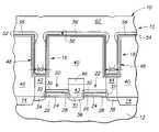
- FIG. 1is a diagrammatic top plan view of a portion of a semiconductor wafer fragment in accordance with an aspect of the invention.
- FIG. 2is a diagrammatic sectional view taken through line 2 — 2 in FIG. 1 .
- FIG. 3is an alternate embodiment view to that depicted by FIG. 2 .
- semiconductor substrateor “semiconductive substrate” is defined to mean any construction comprising semiconductive material, including, but not limited to, bulk semiconductive materials such as a semiconductive wafer (either alone or in assemblies comprising other materials thereon), and semiconductive material layers (either alone or in assemblies comprising other materials).
- substraterefers to any supporting structure, including, but not limited to, the semiconductive substrates described above.
- Substrate fragment 10comprises bulk monocrystalline silicon 12 having trench isolation regions 14 formed therein. Of course, alternate semiconductor substrates (for example semiconductor-on-insulator) are contemplated, and whether existing or yet-to-be developed.
- the particular exemplary illustrated memory circuitrydepicts two memory cells of DRAM circuitry, and particularly, buried digit line DRAM circuitry.
- any memory circuitryis contemplated, whether existing or yet-to-be developed, that at least includes some memory array which comprises a plurality of memory cell capacitors, and as will be apparent from the continuing discussion.
- Substrate fragment 10depicts a portion of a memory array 15 comprising a plurality of capacitors, with two such capacitors 16 and 18 being shown.
- a pair of wordlines 20 and 22is depicted as being received over semiconductive material 12 .
- suchare depicted as comprising a gate dielectric layer 24 , a conductively doped polysilicon layer 26 received thereover, a more conductive refractory metal or refractory metal silicide layer 28 received thereover, and an insulative cap 30 (i.e., silicon nitride) received over layer 28 .
- Anisotropically etched sidewall spacers 32are shown insulating the sidewalls of wordlines 20 and 22 .
- Conductive diffusion regions 34 , 36 and 38are provided within semiconductive material 12 .
- Diffusion region 36is received between wordlines 20 and 22 , and constitutes a shared bit node/junction for the two memory cells.
- Diffusion regions 34 and 38are received laterally outward of wordlines 20 and 22 , respectively, and comprise storage node junctions for the two depicted memory cells.
- One or more insulative materials 40have been formed over substrate 12 , including wordlines 20 and 22 , in the depicted exemplary embodiment.
- An exemplary preferred material or materialsinclude silicon dioxides including, most preferably, insulative silicate glasses such as BPSG and phosphosilicate glass (PSG).
- PSGphosphosilicate glass
- Conductive contacts or plugs 42 , 43 and 44are depicted as being received within material or materials 40 , and extend to diffusion regions 34 , 36 and 38 , respectively.
- Suchmight comprise one or more conductive materials, for example conductively doped polysilicon, titanium nitride and titanium silicide.
- Materials 42 , 43 and 44might be the same as one another or different. By way of example only, such might be formed within contact openings formed after an initial deposition of undoped silicon dioxide followed by the deposition of BPSG.
- FIGS. 1 and 2also depict a buried digit line 46 with respect to the exemplary memory circuitry being described.
- Individual capacitors 16 and 18are depicted as comprising a storage node electrode 48 , a capacitor dielectric region 50 , and a cell electrode 52 .
- Cell electrode 52is commonly shared among at least some of the plurality of memory cell capacitors within the memory array, with FIG. 2 depicting cell electrode 52 being shared by memory cell capacitors 16 and 18 within memory array 15 .
- An exemplary preferred storage node electrode materialis a conductive metal nitride, for example titanium nitride.
- Such electrodesmight comprise, consist essentially of, or consist of an exemplary conductive metal nitride.
- alternate exemplary conductive metal nitridesinclude tungsten nitride, titanium boron nitride, and tantalum nitride.
- An exemplary preferred thickness range for storage node 48is from 50 Angstroms to 100 Angstroms.
- storage node electrodes 48comprise a container shape. Further in one preferred embodiment, such container shaped storage node electrodes are received within container openings formed within an insulative silicate glass, such as the depicted exemplary material 40 .
- An exemplary preferred capacitor dielectric region 50comprises at least one of aluminum oxide and hafnium oxide.
- further exemplary preferred dielectricsinclude tantalum oxides, tantalates, titanates such as barium strontium titanate, and oxide-nitride-oxide (ONO) materials.
- cell electrode 52comprises a conductive metal nitride layer 54 and a conductor metal layer 56 comprising at least one of elemental tungsten, a tungsten alloy, tungsten silicide and tungsten nitride, where the conductor metal layer is different in composition from conductive metal nitride layer 54 .
- An exemplary tungsten alloyis titanium-tungsten.
- conductor metal layer 56is received over conductive metal nitride layer 54 (and “on” such layer as shown, meaning in at least some physical contacting relationship therewith).
- the inventioncontemplates the reverse whereby conductive metal nitride layer 54 is received over a conductor metal layer, including on such layer.
- exemplary preferred conductive metal nitride layersare those described above in connection with preferred storage node materials.
- An exemplary preferred thickness range for conductive metal nitride layer 54is from 100 Angstroms to 300 Angstroms, with 200 Angstroms being a specific preferred example.
- Conductor metal layer 56might be received over all (not shown) of each individual of storage node electrodes 48 of the plurality of memory cell capacitors as in the prior art described in the “Background” section. Alternately as shown, conductor metal layer 56 is received over only a portion of each individual of storage node electrodes 48 of capacitors 16 and 18 . For example and by way of example only, conductor metal layer 56 is shown as not being received over a central portion 60 of storage nodes 48 at the base of the depicted container shapes.
- conductive metal nitride layer 54is received over all of each individual of the storage node electrodes 48 of at least some of the plurality of memory cell capacitors, with layer 54 being shown as being received over all of storage node electrodes 48 of capacitors 16 and 18 .
- An exemplary preferred thickness range for conductor metal layer 56is from 100 Angstroms to 1,000 Angstroms.
- polysilicon 62is received over both of conductive metal nitride layer 54 and conductor metal layer 56 , with conductive metal nitride layer 54 , conductor metal layer 56 and polysilicon 62 being received over storage node electrodes 48 of memory cell capacitors 16 and 18 . Further in one preferred embodiment, and where conductor metal layer 56 is received over a conductive metal nitride layer 54 , polysilicon 62 is received on the at least one of elemental tungsten, tungsten alloy, tungsten silicide or tungsten nitride of conductor metal layer 56 .
- polysilicon 62is also received on conductive metal nitride 54 . If conductor metal layer 56 is received over all of each individual of storage node electrodes 48 of the plurality of memory cell capacitors, polysilicon 62 might be received on only one of the conductive metal nitride layer or conductor metal layer. Regardless, an exemplary preferred thickness range for polysilicon 62 is from 50 Angstroms to 600 Angstroms, and preferably fills the remaining volume of the depicted storage node container shapes. Further in the depicted preferred embodiment, polysilicon 62 is laterally co-extensive with conductive metal nitride 54 , at least within memory array 15 , for example as shown in FIG. 2 .
- Polysilicon 62might be conductively doped with a conductivity enhancing impurity, for example whereby polysilicon 62 might comprise an operative electrically conductive part or portion of the cell electrode. Alternately by way of example only, the polysilicon might be doped with a conductivity enhancing impurity insufficient to render the polysilicon effectively conductive to comprise a conductive part of the cell electrode, and in one embodiment, might not be conductively doped with any conductivity enhancing impurity.
- the inventionalso contemplates polysilicon being received over conductor metal layer 56 (whether such is partially as depicted or wholly as not depicted received over each individual storage node electrode) even if, or regardless of whether, conductive metal nitride layer 54 is present.
- conductor metal layer 56is received over conductive metal nitride layer 54 .
- the inventioncontemplates the conductor metal layer comprising at least two of elemental tungsten, a tungsten alloy, tungsten silicide and tungsten nitride, including any two, three or four thereof.
- FIG. 3depicts an alternate embodiment semiconductor wafer fragment 10 a . Like numerals from the first described embodiment are utilized where appropriate, with differences being indicated with the suffix “a”, or with different numerals.
- FIG. 3depicts a cell electrode 52 a comprising a conductor metal layer 56 a comprised of two layers 55 and 57 comprising any two of elemental tungsten, a tungsten alloy, tungsten silicide and tungsten nitride. Other preferred attributes are as describe above, and of course, three or four of such layers (including more of other layers) might be utilized.
Landscapes
- Engineering & Computer Science (AREA)
- Manufacturing & Machinery (AREA)
- Semiconductor Memories (AREA)
- Semiconductor Integrated Circuits (AREA)
Abstract
Description
Claims (58)
Priority Applications (7)
| Application Number | Priority Date | Filing Date | Title |
|---|---|---|---|
| US10/918,613US7126182B2 (en) | 2004-08-13 | 2004-08-13 | Memory circuitry |
| EP05785656AEP1787317A2 (en) | 2004-08-13 | 2005-08-11 | Memory circuitry |
| CNA200580027152XACN101002298A (en) | 2004-08-13 | 2005-08-11 | Memory circuitry |
| JP2007525812AJP5417596B2 (en) | 2004-08-13 | 2005-08-11 | Memory circuit |
| PCT/US2005/028670WO2006020828A2 (en) | 2004-08-13 | 2005-08-11 | Top electrode for a dram capacitor |
| TW094127599ATWI285941B (en) | 2004-08-13 | 2005-08-12 | Memory circuitry |
| US11/481,660US7495277B2 (en) | 2004-08-13 | 2006-07-05 | Memory circuitry |
Applications Claiming Priority (1)
| Application Number | Priority Date | Filing Date | Title |
|---|---|---|---|
| US10/918,613US7126182B2 (en) | 2004-08-13 | 2004-08-13 | Memory circuitry |
Related Child Applications (1)
| Application Number | Title | Priority Date | Filing Date |
|---|---|---|---|
| US11/481,660ContinuationUS7495277B2 (en) | 2004-08-13 | 2006-07-05 | Memory circuitry |
Publications (2)
| Publication Number | Publication Date |
|---|---|
| US20060033140A1 US20060033140A1 (en) | 2006-02-16 |
| US7126182B2true US7126182B2 (en) | 2006-10-24 |
Family
ID=35520704
Family Applications (2)
| Application Number | Title | Priority Date | Filing Date |
|---|---|---|---|
| US10/918,613Expired - Fee RelatedUS7126182B2 (en) | 2004-08-13 | 2004-08-13 | Memory circuitry |
| US11/481,660Expired - Fee RelatedUS7495277B2 (en) | 2004-08-13 | 2006-07-05 | Memory circuitry |
Family Applications After (1)
| Application Number | Title | Priority Date | Filing Date |
|---|---|---|---|
| US11/481,660Expired - Fee RelatedUS7495277B2 (en) | 2004-08-13 | 2006-07-05 | Memory circuitry |
Country Status (6)
| Country | Link |
|---|---|
| US (2) | US7126182B2 (en) |
| EP (1) | EP1787317A2 (en) |
| JP (1) | JP5417596B2 (en) |
| CN (1) | CN101002298A (en) |
| TW (1) | TWI285941B (en) |
| WO (1) | WO2006020828A2 (en) |
Cited By (2)
| Publication number | Priority date | Publication date | Assignee | Title |
|---|---|---|---|---|
| US20060249772A1 (en)* | 2004-08-13 | 2006-11-09 | Graettinger Thomas M | Memory circuitry |
| US20080274615A1 (en)* | 2007-05-02 | 2008-11-06 | Vaartstra Brian A | Atomic Layer Deposition Methods, Methods of Forming Dielectric Materials, Methods of Forming Capacitors, And Methods of Forming DRAM Unit Cells |
Families Citing this family (2)
| Publication number | Priority date | Publication date | Assignee | Title |
|---|---|---|---|---|
| KR100791339B1 (en)* | 2006-08-25 | 2008-01-03 | 삼성전자주식회사 | Composite chip semiconductor device including planarization resistance pattern and manufacturing method |
| US8779849B2 (en)* | 2012-01-27 | 2014-07-15 | Micron Technology, Inc. | Apparatuses and methods for providing capacitance in a multi-chip module |
Citations (33)
| Publication number | Priority date | Publication date | Assignee | Title |
|---|---|---|---|---|
| US5766994A (en)* | 1997-04-11 | 1998-06-16 | Vanguard International Semiconductor Corporation | Dynamic random access memory fabrication method having stacked capacitors with increased capacitance |
| US5843830A (en) | 1996-06-26 | 1998-12-01 | Micron Technology, Inc. | Capacitor, and methods for forming a capacitor |
| US5930639A (en) | 1996-04-08 | 1999-07-27 | Micron Technology, Inc. | Method for precision etching of platinum electrodes |
| US5960294A (en)* | 1998-01-13 | 1999-09-28 | Micron Technology, Inc. | Method of fabricating a semiconductor device utilizing polysilicon grains |
| US5981334A (en)* | 1997-08-21 | 1999-11-09 | Chien; Sun-Chieh | Method of fabricating DRAM capacitor |
| US6033950A (en) | 1998-04-10 | 2000-03-07 | Taiwan Semiconductor Manufacturing Company, Ltd. | Dual layer poly deposition to prevent auto-doping in mixed-mode product fabrication |
| US6049101A (en) | 1997-06-23 | 2000-04-11 | Micron Technology, Inc. | Processing methods of forming a capacitor, and capacitor construction |
| US6093617A (en)* | 1997-05-19 | 2000-07-25 | Taiwan Semiconductor Manufacturing Company | Process to fabricate hemispherical grain polysilicon |
| US6265260B1 (en)* | 1999-01-12 | 2001-07-24 | Lucent Technologies Inc. | Method for making an integrated circuit capacitor including tantalum pentoxide |
| US6309973B1 (en) | 1998-02-27 | 2001-10-30 | Micron Technology, Inc. | Semiconductor processing methods of forming a conductive projection and methods of increasing alignment tolerances |
| US20010044181A1 (en) | 1996-11-06 | 2001-11-22 | Fujitsu Limited | Semiconductor device and method for fabricating the same |
| US6340622B1 (en) | 1999-11-09 | 2002-01-22 | Hyundai Electronics Industries Co., Ltd. | Method for fabricating capacitors of semiconductor device |
| US6348709B1 (en) | 1999-03-15 | 2002-02-19 | Micron Technology, Inc. | Electrical contact for high dielectric constant capacitors and method for fabricating the same |
| US20020025680A1 (en) | 1999-07-23 | 2002-02-28 | New Daryl C. | Methods of etching insulative materials, of forming electrical devices, and of forming capacitors |
| US6372667B1 (en) | 1999-06-25 | 2002-04-16 | Hyundai Electronics Industries Co., Ltd. | Method of manufacturing a capacitor for semiconductor memory devices |
| US6403413B2 (en)* | 2000-07-14 | 2002-06-11 | Hitachi, Ltd. | Manufacturing method of semiconductor integrated circuit device having a capacitor |
| US20020084480A1 (en)* | 2000-08-31 | 2002-07-04 | Cem Basceri | Top electrode in a strongly oxidizing environment |
| US20020160565A1 (en)* | 2001-04-30 | 2002-10-31 | Lee Kee Jeung | Capacitor for semiconductor devices and a method of fabricating such capacitors |
| US20020160559A1 (en) | 2001-04-30 | 2002-10-31 | Lee Kee Jeung | Capacitor for semiconductor devices and a method of fabrication |
| US6482736B1 (en) | 2000-06-08 | 2002-11-19 | Micron Technology, Inc. | Methods for forming and integrated circuit structures containing enhanced-surface-area conductive layers |
| US6492241B1 (en) | 2000-04-10 | 2002-12-10 | Micron Technology, Inc. | Integrated capacitors fabricated with conductive metal oxides |
| US6518117B2 (en)* | 2001-03-29 | 2003-02-11 | Micron Technology, Inc. | Methods of forming nitrogen-containing masses, silicon nitride layers, and capacitor constructions |
| US20030178665A1 (en)* | 2002-03-19 | 2003-09-25 | Nec Electronics Corporation | Semiconductor device with improved capacitive element and method of forming the same |
| US20030199139A1 (en)* | 2002-04-23 | 2003-10-23 | Kee Jeung Lee | Capacitor in semiconductor device having dual dielectric film structure and method for fabricating the same |
| US6689657B2 (en) | 1999-04-06 | 2004-02-10 | Micron Technology, Inc. | Method of forming a capacitor |
| US20040053474A1 (en) | 2002-09-17 | 2004-03-18 | Dong-Woo Shin | Capacitor and method for fabricating the same |
| US20040137678A1 (en) | 2002-12-30 | 2004-07-15 | Cho Ho Jin | Method for forming capacitor of semiconductor device |
| US6825081B2 (en)* | 2001-07-24 | 2004-11-30 | Micron Technology, Inc. | Cell nitride nucleation on insulative layers and reduced corner leakage of container capacitors |
| US20040248362A1 (en)* | 2003-02-14 | 2004-12-09 | Elpida Memory, Inc. | Semiconductor device and fabrication method therefor |
| US6967154B2 (en)* | 2002-08-26 | 2005-11-22 | Micron Technology, Inc. | Enhanced atomic layer deposition |
| US6967135B1 (en)* | 2004-06-30 | 2005-11-22 | Hynix Semiconductor Inc. | Method of forming capacitor of semiconductor device |
| US20050268618A1 (en) | 2004-06-08 | 2005-12-08 | General Electric Company | Burner tube and method for mixing air and gas in a gas turbine engine |
| US20060020828A1 (en) | 2003-05-29 | 2006-01-26 | Fujitsu Limited | Data restoring method, information processing apparatus, and computer-readable recording medium recording data restoring program |
Family Cites Families (2)
| Publication number | Priority date | Publication date | Assignee | Title |
|---|---|---|---|---|
| JP3464956B2 (en)* | 1999-12-09 | 2003-11-10 | Necエレクトロニクス株式会社 | Semiconductor device |
| US7126182B2 (en)* | 2004-08-13 | 2006-10-24 | Micron Technology, Inc. | Memory circuitry |
- 2004
- 2004-08-13USUS10/918,613patent/US7126182B2/ennot_activeExpired - Fee Related
- 2005
- 2005-08-11WOPCT/US2005/028670patent/WO2006020828A2/enactiveApplication Filing
- 2005-08-11CNCNA200580027152XApatent/CN101002298A/enactivePending
- 2005-08-11EPEP05785656Apatent/EP1787317A2/ennot_activeWithdrawn
- 2005-08-11JPJP2007525812Apatent/JP5417596B2/ennot_activeExpired - Fee Related
- 2005-08-12TWTW094127599Apatent/TWI285941B/ennot_activeIP Right Cessation
- 2006
- 2006-07-05USUS11/481,660patent/US7495277B2/ennot_activeExpired - Fee Related
Patent Citations (41)
| Publication number | Priority date | Publication date | Assignee | Title |
|---|---|---|---|---|
| US5930639A (en) | 1996-04-08 | 1999-07-27 | Micron Technology, Inc. | Method for precision etching of platinum electrodes |
| US5843830A (en) | 1996-06-26 | 1998-12-01 | Micron Technology, Inc. | Capacitor, and methods for forming a capacitor |
| US5844771A (en) | 1996-06-26 | 1998-12-01 | Micron Technology, Inc. | Capacitor construction |
| US6171925B1 (en) | 1996-06-26 | 2001-01-09 | Micron Technology, Inc. | Capacitor, and methods for forming a capacitor |
| US20010044181A1 (en) | 1996-11-06 | 2001-11-22 | Fujitsu Limited | Semiconductor device and method for fabricating the same |
| US5766994A (en)* | 1997-04-11 | 1998-06-16 | Vanguard International Semiconductor Corporation | Dynamic random access memory fabrication method having stacked capacitors with increased capacitance |
| US6093617A (en)* | 1997-05-19 | 2000-07-25 | Taiwan Semiconductor Manufacturing Company | Process to fabricate hemispherical grain polysilicon |
| US6580114B1 (en) | 1997-06-23 | 2003-06-17 | Micron Technology, Inc. | Processing methods of forming a capacitor, and capacitor construction |
| US6049101A (en) | 1997-06-23 | 2000-04-11 | Micron Technology, Inc. | Processing methods of forming a capacitor, and capacitor construction |
| US6146961A (en) | 1997-06-23 | 2000-11-14 | Micron Technology, Inc. | Processing methods of forming a capacitor |
| US5981334A (en)* | 1997-08-21 | 1999-11-09 | Chien; Sun-Chieh | Method of fabricating DRAM capacitor |
| US5960294A (en)* | 1998-01-13 | 1999-09-28 | Micron Technology, Inc. | Method of fabricating a semiconductor device utilizing polysilicon grains |
| US6309973B1 (en) | 1998-02-27 | 2001-10-30 | Micron Technology, Inc. | Semiconductor processing methods of forming a conductive projection and methods of increasing alignment tolerances |
| US6297528B1 (en) | 1998-04-10 | 2001-10-02 | Taiwan Semiconductor Mfg | Dual layer poly deposition to prevent auto-doping in mixed-mode product fabrication |
| US6033950A (en) | 1998-04-10 | 2000-03-07 | Taiwan Semiconductor Manufacturing Company, Ltd. | Dual layer poly deposition to prevent auto-doping in mixed-mode product fabrication |
| US6265260B1 (en)* | 1999-01-12 | 2001-07-24 | Lucent Technologies Inc. | Method for making an integrated circuit capacitor including tantalum pentoxide |
| US6348709B1 (en) | 1999-03-15 | 2002-02-19 | Micron Technology, Inc. | Electrical contact for high dielectric constant capacitors and method for fabricating the same |
| US6696718B1 (en) | 1999-04-06 | 2004-02-24 | Micron Technology, Inc. | Capacitor having an electrode formed from a transition metal or a conductive metal-oxide, and method of forming same |
| US6689657B2 (en) | 1999-04-06 | 2004-02-10 | Micron Technology, Inc. | Method of forming a capacitor |
| US6372667B1 (en) | 1999-06-25 | 2002-04-16 | Hyundai Electronics Industries Co., Ltd. | Method of manufacturing a capacitor for semiconductor memory devices |
| US20020025680A1 (en) | 1999-07-23 | 2002-02-28 | New Daryl C. | Methods of etching insulative materials, of forming electrical devices, and of forming capacitors |
| US6358857B1 (en) | 1999-07-23 | 2002-03-19 | Micron Technology, Inc. | Methods of etching insulative materials, of forming electrical devices, and of forming capacitors |
| US6340622B1 (en) | 1999-11-09 | 2002-01-22 | Hyundai Electronics Industries Co., Ltd. | Method for fabricating capacitors of semiconductor device |
| US6492241B1 (en) | 2000-04-10 | 2002-12-10 | Micron Technology, Inc. | Integrated capacitors fabricated with conductive metal oxides |
| US6482736B1 (en) | 2000-06-08 | 2002-11-19 | Micron Technology, Inc. | Methods for forming and integrated circuit structures containing enhanced-surface-area conductive layers |
| US6403413B2 (en)* | 2000-07-14 | 2002-06-11 | Hitachi, Ltd. | Manufacturing method of semiconductor integrated circuit device having a capacitor |
| US20020084480A1 (en)* | 2000-08-31 | 2002-07-04 | Cem Basceri | Top electrode in a strongly oxidizing environment |
| US6682969B1 (en) | 2000-08-31 | 2004-01-27 | Micron Technology, Inc. | Top electrode in a strongly oxidizing environment |
| US6518117B2 (en)* | 2001-03-29 | 2003-02-11 | Micron Technology, Inc. | Methods of forming nitrogen-containing masses, silicon nitride layers, and capacitor constructions |
| US20020160565A1 (en)* | 2001-04-30 | 2002-10-31 | Lee Kee Jeung | Capacitor for semiconductor devices and a method of fabricating such capacitors |
| US20020160559A1 (en) | 2001-04-30 | 2002-10-31 | Lee Kee Jeung | Capacitor for semiconductor devices and a method of fabrication |
| US6825081B2 (en)* | 2001-07-24 | 2004-11-30 | Micron Technology, Inc. | Cell nitride nucleation on insulative layers and reduced corner leakage of container capacitors |
| US20030178665A1 (en)* | 2002-03-19 | 2003-09-25 | Nec Electronics Corporation | Semiconductor device with improved capacitive element and method of forming the same |
| US20030199139A1 (en)* | 2002-04-23 | 2003-10-23 | Kee Jeung Lee | Capacitor in semiconductor device having dual dielectric film structure and method for fabricating the same |
| US6967154B2 (en)* | 2002-08-26 | 2005-11-22 | Micron Technology, Inc. | Enhanced atomic layer deposition |
| US20040053474A1 (en) | 2002-09-17 | 2004-03-18 | Dong-Woo Shin | Capacitor and method for fabricating the same |
| US20040137678A1 (en) | 2002-12-30 | 2004-07-15 | Cho Ho Jin | Method for forming capacitor of semiconductor device |
| US20040248362A1 (en)* | 2003-02-14 | 2004-12-09 | Elpida Memory, Inc. | Semiconductor device and fabrication method therefor |
| US20060020828A1 (en) | 2003-05-29 | 2006-01-26 | Fujitsu Limited | Data restoring method, information processing apparatus, and computer-readable recording medium recording data restoring program |
| US20050268618A1 (en) | 2004-06-08 | 2005-12-08 | General Electric Company | Burner tube and method for mixing air and gas in a gas turbine engine |
| US6967135B1 (en)* | 2004-06-30 | 2005-11-22 | Hynix Semiconductor Inc. | Method of forming capacitor of semiconductor device |
Cited By (3)
| Publication number | Priority date | Publication date | Assignee | Title |
|---|---|---|---|---|
| US20060249772A1 (en)* | 2004-08-13 | 2006-11-09 | Graettinger Thomas M | Memory circuitry |
| US7495277B2 (en)* | 2004-08-13 | 2009-02-24 | Micron Technology, Inc. | Memory circuitry |
| US20080274615A1 (en)* | 2007-05-02 | 2008-11-06 | Vaartstra Brian A | Atomic Layer Deposition Methods, Methods of Forming Dielectric Materials, Methods of Forming Capacitors, And Methods of Forming DRAM Unit Cells |
Also Published As
| Publication number | Publication date |
|---|---|
| US7495277B2 (en) | 2009-02-24 |
| WO2006020828A2 (en) | 2006-02-23 |
| JP5417596B2 (en) | 2014-02-19 |
| EP1787317A2 (en) | 2007-05-23 |
| US20060249772A1 (en) | 2006-11-09 |
| TW200620564A (en) | 2006-06-16 |
| TWI285941B (en) | 2007-08-21 |
| WO2006020828A3 (en) | 2006-04-13 |
| JP2008510306A (en) | 2008-04-03 |
| CN101002298A (en) | 2007-07-18 |
| US20060033140A1 (en) | 2006-02-16 |
Similar Documents
| Publication | Publication Date | Title |
|---|---|---|
| US6388284B2 (en) | Capacitor structures | |
| US6475855B1 (en) | Method of forming integrated circuitry, method of forming a capacitor and method of forming DRAM integrated circuitry | |
| US6451661B1 (en) | DRAM capacitor formulation using a double-sided electrode | |
| US9230966B2 (en) | Capacitor and method of manufacturing the same | |
| JP3878724B2 (en) | Semiconductor integrated circuit device and manufacturing method thereof | |
| US6479855B1 (en) | Capacitor and conductive line constructions and semiconductor processing methods of forming capacitors and conductive lines | |
| US20070018224A1 (en) | Devices and methods for preventing capacitor leakage | |
| US6764863B2 (en) | Memory-storage node and the method of fabricating the same | |
| US6849894B2 (en) | Semiconductor device with transistor and capacitor and its manufacture method | |
| US6518121B2 (en) | Boride electrodes and barriers for cell dielectrics | |
| US7495277B2 (en) | Memory circuitry | |
| US7030442B2 (en) | Stack-film trench capacitor and method for manufacturing the same | |
| US6030867A (en) | Method of fabricating a Fin/HSG DRAM cell capacitor | |
| US20230006030A1 (en) | Semiconductor structure and manufacturing method thereof | |
| KR100888123B1 (en) | Memory circuit | |
| KR100313084B1 (en) | Method for manufacturing a semiconductor device | |
| JPH10173151A (en) | Semiconductor integrated circuit device and method of manufacturing the same | |
| KR20060114220A (en) | Manufacturing method of semiconductor device |
Legal Events
| Date | Code | Title | Description |
|---|---|---|---|
| AS | Assignment | Owner name:MICRON TECHNOLOGY, INC., IDAHO Free format text:ASSIGNMENT OF ASSIGNORS INTEREST;ASSIGNOR:GRAETTINGER, THOMAS M.;REEL/FRAME:015705/0476 Effective date:20040810 | |
| FEPP | Fee payment procedure | Free format text:PAYOR NUMBER ASSIGNED (ORIGINAL EVENT CODE: ASPN); ENTITY STATUS OF PATENT OWNER: LARGE ENTITY | |
| CC | Certificate of correction | ||
| AS | Assignment | Owner name:ROUND ROCK RESEARCH, LLC,NEW YORK Free format text:ASSIGNMENT OF ASSIGNORS INTEREST;ASSIGNOR:MICRON TECHNOLOGY, INC.;REEL/FRAME:023786/0416 Effective date:20091223 Owner name:ROUND ROCK RESEARCH, LLC, NEW YORK Free format text:ASSIGNMENT OF ASSIGNORS INTEREST;ASSIGNOR:MICRON TECHNOLOGY, INC.;REEL/FRAME:023786/0416 Effective date:20091223 | |
| FPAY | Fee payment | Year of fee payment:4 | |
| FPAY | Fee payment | Year of fee payment:8 | |
| FEPP | Fee payment procedure | Free format text:MAINTENANCE FEE REMINDER MAILED (ORIGINAL EVENT CODE: REM.) | |
| LAPS | Lapse for failure to pay maintenance fees | Free format text:PATENT EXPIRED FOR FAILURE TO PAY MAINTENANCE FEES (ORIGINAL EVENT CODE: EXP.); ENTITY STATUS OF PATENT OWNER: LARGE ENTITY | |
| STCH | Information on status: patent discontinuation | Free format text:PATENT EXPIRED DUE TO NONPAYMENT OF MAINTENANCE FEES UNDER 37 CFR 1.362 | |
| FP | Lapsed due to failure to pay maintenance fee | Effective date:20181024 |