US7123216B1 - Photonic MEMS and structures - Google Patents
Photonic MEMS and structuresDownload PDFInfo
- Publication number
- US7123216B1 US7123216B1US09/413,222US41322299AUS7123216B1US 7123216 B1US7123216 B1US 7123216B1US 41322299 AUS41322299 AUS 41322299AUS 7123216 B1US7123216 B1US 7123216B1
- Authority
- US
- United States
- Prior art keywords
- imod
- substrate
- voltages
- light
- optical
- Prior art date
- Legal status (The legal status is an assumption and is not a legal conclusion. Google has not performed a legal analysis and makes no representation as to the accuracy of the status listed.)
- Expired - Fee Related
Links
- 238000000034methodMethods0.000claimsabstractdescription73
- 230000003252repetitive effectEffects0.000claimsdescription2
- 230000003287optical effectEffects0.000abstractdescription75
- 239000000463materialSubstances0.000abstractdescription72
- 238000004519manufacturing processMethods0.000abstractdescription39
- 230000008569processEffects0.000abstractdescription30
- 238000000576coating methodMethods0.000abstractdescription21
- 238000013459approachMethods0.000abstractdescription15
- 238000003491arrayMethods0.000abstractdescription12
- 230000006870functionEffects0.000abstractdescription12
- 238000012360testing methodMethods0.000abstractdescription9
- 230000000153supplemental effectEffects0.000abstractdescription7
- 238000004806packaging method and processMethods0.000abstractdescription3
- 238000011156evaluationMethods0.000abstractdescription2
- 239000011159matrix materialSubstances0.000abstractdescription2
- 239000000758substrateSubstances0.000description123
- 239000010408filmSubstances0.000description75
- 239000010410layerSubstances0.000description41
- 238000013461designMethods0.000description38
- 239000012528membraneSubstances0.000description35
- 229910052751metalInorganic materials0.000description21
- 239000002184metalSubstances0.000description21
- 230000001902propagating effectEffects0.000description21
- 239000011521glassSubstances0.000description17
- VYPSYNLAJGMNEJ-UHFFFAOYSA-NSilicium dioxideChemical compoundO=[Si]=OVYPSYNLAJGMNEJ-UHFFFAOYSA-N0.000description16
- 230000007547defectEffects0.000description16
- 238000010586diagramMethods0.000description16
- 239000000047productSubstances0.000description16
- 239000011248coating agentSubstances0.000description15
- XUIMIQQOPSSXEZ-UHFFFAOYSA-NSiliconChemical compound[Si]XUIMIQQOPSSXEZ-UHFFFAOYSA-N0.000description14
- 229910052782aluminiumInorganic materials0.000description14
- XAGFODPZIPBFFR-UHFFFAOYSA-NaluminiumChemical compound[Al]XAGFODPZIPBFFR-UHFFFAOYSA-N0.000description14
- 239000010703siliconSubstances0.000description14
- 230000006399behaviorEffects0.000description13
- 229910052710siliconInorganic materials0.000description13
- 230000004044responseEffects0.000description12
- 238000010168coupling processMethods0.000description11
- 238000005859coupling reactionMethods0.000description11
- 239000006096absorbing agentSubstances0.000description10
- 239000010409thin filmSubstances0.000description10
- 238000000151depositionMethods0.000description9
- 230000000737periodic effectEffects0.000description9
- 230000008021depositionEffects0.000description8
- 239000000049pigmentSubstances0.000description8
- 235000012239silicon dioxideNutrition0.000description8
- 239000000377silicon dioxideSubstances0.000description8
- 239000003086colorantSubstances0.000description7
- 239000004020conductorSubstances0.000description7
- 230000005855radiationEffects0.000description7
- 230000000694effectsEffects0.000description6
- 239000000835fiberSubstances0.000description6
- 150000002739metalsChemical class0.000description6
- 229920003023plasticPolymers0.000description6
- 229920000642polymerPolymers0.000description6
- 239000004065semiconductorSubstances0.000description6
- 230000008859changeEffects0.000description5
- 239000012212insulatorSubstances0.000description5
- 239000004033plasticSubstances0.000description5
- 238000012545processingMethods0.000description5
- 125000006850spacer groupChemical group0.000description5
- 235000012431wafersNutrition0.000description5
- 230000015572biosynthetic processEffects0.000description4
- PCHJSUWPFVWCPO-UHFFFAOYSA-NgoldChemical compound[Au]PCHJSUWPFVWCPO-UHFFFAOYSA-N0.000description4
- 229910052737goldInorganic materials0.000description4
- 239000010931goldSubstances0.000description4
- 229910001507metal halideInorganic materials0.000description4
- 150000005309metal halidesChemical class0.000description4
- 239000004038photonic crystalSubstances0.000description4
- 229920002120photoresistant polymerPolymers0.000description4
- BASFCYQUMIYNBI-UHFFFAOYSA-NplatinumChemical compound[Pt]BASFCYQUMIYNBI-UHFFFAOYSA-N0.000description4
- 230000003068static effectEffects0.000description4
- 229910000838Al alloyInorganic materials0.000description3
- QGJOPFRUJISHPQ-UHFFFAOYSA-NCarbon disulfideChemical compoundS=C=SQGJOPFRUJISHPQ-UHFFFAOYSA-N0.000description3
- VYZAMTAEIAYCRO-UHFFFAOYSA-NChromiumChemical compound[Cr]VYZAMTAEIAYCRO-UHFFFAOYSA-N0.000description3
- 229910052804chromiumInorganic materials0.000description3
- 239000011651chromiumSubstances0.000description3
- 229910052681coesiteInorganic materials0.000description3
- 239000000470constituentSubstances0.000description3
- 230000008878couplingEffects0.000description3
- 229910052906cristobaliteInorganic materials0.000description3
- 238000005516engineering processMethods0.000description3
- 238000003384imaging methodMethods0.000description3
- 238000010884ion-beam techniqueMethods0.000description3
- 238000005259measurementMethods0.000description3
- -1oxidesSubstances0.000description3
- 238000000059patterningMethods0.000description3
- 238000001020plasma etchingMethods0.000description3
- NLKNQRATVPKPDG-UHFFFAOYSA-Mpotassium iodideChemical compound[K+].[I-]NLKNQRATVPKPDG-UHFFFAOYSA-M0.000description3
- 230000002829reductive effectEffects0.000description3
- 238000001338self-assemblyMethods0.000description3
- 229910052682stishoviteInorganic materials0.000description3
- 229910052905tridymiteInorganic materials0.000description3
- WFKWXMTUELFFGS-UHFFFAOYSA-NtungstenChemical compound[W]WFKWXMTUELFFGS-UHFFFAOYSA-N0.000description3
- 229910052721tungstenInorganic materials0.000description3
- 239000010937tungstenSubstances0.000description3
- PXHVJJICTQNCMI-UHFFFAOYSA-NNickelChemical compound[Ni]PXHVJJICTQNCMI-UHFFFAOYSA-N0.000description2
- GWEVSGVZZGPLCZ-UHFFFAOYSA-NTitan oxideChemical compoundO=[Ti]=OGWEVSGVZZGPLCZ-UHFFFAOYSA-N0.000description2
- 238000000429assemblyMethods0.000description2
- 230000000712assemblyEffects0.000description2
- 230000008901benefitEffects0.000description2
- 230000005540biological transmissionEffects0.000description2
- 238000003486chemical etchingMethods0.000description2
- 230000000295complement effectEffects0.000description2
- 230000006835compressionEffects0.000description2
- 238000007906compressionMethods0.000description2
- 238000007796conventional methodMethods0.000description2
- 229920001577copolymerPolymers0.000description2
- 230000001419dependent effectEffects0.000description2
- 238000004090dissolutionMethods0.000description2
- 230000008020evaporationEffects0.000description2
- 238000001704evaporationMethods0.000description2
- 229910052732germaniumInorganic materials0.000description2
- GNPVGFCGXDBREM-UHFFFAOYSA-Ngermanium atomChemical compound[Ge]GNPVGFCGXDBREM-UHFFFAOYSA-N0.000description2
- 238000010348incorporationMethods0.000description2
- ORUIBWPALBXDOA-UHFFFAOYSA-Lmagnesium fluorideChemical compound[F-].[F-].[Mg+2]ORUIBWPALBXDOA-UHFFFAOYSA-L0.000description2
- 229910001635magnesium fluorideInorganic materials0.000description2
- 238000005459micromachiningMethods0.000description2
- 239000011368organic materialSubstances0.000description2
- 239000003973paintSubstances0.000description2
- 229910052697platinumInorganic materials0.000description2
- 229920000747poly(lactic acid)Polymers0.000description2
- 238000007639printingMethods0.000description2
- 238000002310reflectometryMethods0.000description2
- 238000007789sealingMethods0.000description2
- 229910052709silverInorganic materials0.000description2
- 239000004332silverSubstances0.000description2
- 239000002356single layerSubstances0.000description2
- 239000002904solventSubstances0.000description2
- 238000004544sputter depositionMethods0.000description2
- 239000000126substanceSubstances0.000description2
- 229910052724xenonInorganic materials0.000description2
- FHNFHKCVQCLJFQ-UHFFFAOYSA-Nxenon atomChemical compound[Xe]FHNFHKCVQCLJFQ-UHFFFAOYSA-N0.000description2
- JBRZTFJDHDCESZ-UHFFFAOYSA-NAsGaChemical compound[As]#[Ga]JBRZTFJDHDCESZ-UHFFFAOYSA-N0.000description1
- RYGMFSIKBFXOCR-UHFFFAOYSA-NCopperChemical compound[Cu]RYGMFSIKBFXOCR-UHFFFAOYSA-N0.000description1
- GYHNNYVSQQEPJS-UHFFFAOYSA-NGalliumChemical compound[Ga]GYHNNYVSQQEPJS-UHFFFAOYSA-N0.000description1
- 229910001218Gallium arsenideInorganic materials0.000description1
- ZOKXTWBITQBERF-UHFFFAOYSA-NMolybdenumChemical compound[Mo]ZOKXTWBITQBERF-UHFFFAOYSA-N0.000description1
- 239000004642PolyimideSubstances0.000description1
- 239000004793PolystyreneSubstances0.000description1
- BQCADISMDOOEFD-UHFFFAOYSA-NSilverChemical compound[Ag]BQCADISMDOOEFD-UHFFFAOYSA-N0.000description1
- 229910001362Ta alloysInorganic materials0.000description1
- 229910001069Ti alloyInorganic materials0.000description1
- RTAQQCXQSZGOHL-UHFFFAOYSA-NTitaniumChemical compound[Ti]RTAQQCXQSZGOHL-UHFFFAOYSA-N0.000description1
- 229910001080W alloyInorganic materials0.000description1
- 239000005083Zinc sulfideSubstances0.000description1
- 238000010521absorption reactionMethods0.000description1
- WYTGDNHDOZPMIW-RCBQFDQVSA-NalstonineNatural productsC1=CC2=C3C=CC=CC3=NC2=C2N1C[C@H]1[C@H](C)OC=C(C(=O)OC)[C@H]1C2WYTGDNHDOZPMIW-RCBQFDQVSA-N0.000description1
- 229940024548aluminum oxideDrugs0.000description1
- 239000006117anti-reflective coatingSubstances0.000description1
- 230000003667anti-reflective effectEffects0.000description1
- 238000004630atomic force microscopyMethods0.000description1
- 230000002238attenuated effectEffects0.000description1
- 238000004364calculation methodMethods0.000description1
- 230000001413cellular effectEffects0.000description1
- 239000000919ceramicSubstances0.000description1
- 230000005465channelingEffects0.000description1
- 239000007795chemical reaction productSubstances0.000description1
- 239000000084colloidal systemSubstances0.000description1
- 238000005094computer simulationMethods0.000description1
- 238000010276constructionMethods0.000description1
- 229910052802copperInorganic materials0.000description1
- 239000010949copperSubstances0.000description1
- 230000007423decreaseEffects0.000description1
- 230000003247decreasing effectEffects0.000description1
- 238000005137deposition processMethods0.000description1
- 238000011161developmentMethods0.000description1
- 239000003989dielectric materialSubstances0.000description1
- 230000003292diminished effectEffects0.000description1
- 238000006073displacement reactionMethods0.000description1
- 239000007772electrode materialSubstances0.000description1
- 238000004070electrodepositionMethods0.000description1
- 230000005670electromagnetic radiationEffects0.000description1
- 230000005662electromechanicsEffects0.000description1
- 238000004049embossingMethods0.000description1
- 238000005530etchingMethods0.000description1
- 238000011049fillingMethods0.000description1
- 229910052733galliumInorganic materials0.000description1
- 238000005286illuminationMethods0.000description1
- 229910010272inorganic materialInorganic materials0.000description1
- 239000011147inorganic materialSubstances0.000description1
- 230000003993interactionEffects0.000description1
- 150000002500ionsChemical class0.000description1
- 229910052741iridiumInorganic materials0.000description1
- GKOZUEZYRPOHIO-UHFFFAOYSA-Niridium atomChemical compound[Ir]GKOZUEZYRPOHIO-UHFFFAOYSA-N0.000description1
- 238000000608laser ablationMethods0.000description1
- YAFKGUAJYKXPDI-UHFFFAOYSA-Jlead tetrafluorideChemical compoundF[Pb](F)(F)FYAFKGUAJYKXPDI-UHFFFAOYSA-J0.000description1
- 239000006194liquid suspensionSubstances0.000description1
- 238000001459lithographyMethods0.000description1
- 238000003754machiningMethods0.000description1
- 238000012986modificationMethods0.000description1
- 230000004048modificationEffects0.000description1
- 229910052750molybdenumInorganic materials0.000description1
- 239000011733molybdenumSubstances0.000description1
- 229910052759nickelInorganic materials0.000description1
- 230000006911nucleationEffects0.000description1
- 238000010899nucleationMethods0.000description1
- BPUBBGLMJRNUCC-UHFFFAOYSA-Noxygen(2-);tantalum(5+)Chemical compound[O-2].[O-2].[O-2].[O-2].[O-2].[Ta+5].[Ta+5]BPUBBGLMJRNUCC-UHFFFAOYSA-N0.000description1
- 230000036961partial effectEffects0.000description1
- 239000002245particleSubstances0.000description1
- 230000008447perceptionEffects0.000description1
- 230000002093peripheral effectEffects0.000description1
- 238000000206photolithographyMethods0.000description1
- 238000005240physical vapour depositionMethods0.000description1
- 238000000623plasma-assisted chemical vapour depositionMethods0.000description1
- 239000002985plastic filmSubstances0.000description1
- 229920001721polyimidePolymers0.000description1
- 229920002223polystyrenePolymers0.000description1
- 230000000644propagated effectEffects0.000description1
- 239000003870refractory metalSubstances0.000description1
- 229920006395saturated elastomerPolymers0.000description1
- 229910052814silicon oxideInorganic materials0.000description1
- ABTOQLMXBSRXSM-UHFFFAOYSA-Nsilicon tetrafluorideChemical compoundF[Si](F)(F)FABTOQLMXBSRXSM-UHFFFAOYSA-N0.000description1
- 239000007787solidSubstances0.000description1
- 230000003595spectral effectEffects0.000description1
- 238000001228spectrumMethods0.000description1
- 230000007480spreadingEffects0.000description1
- 238000003892spreadingMethods0.000description1
- 238000003860storageMethods0.000description1
- 230000001360synchronised effectEffects0.000description1
- 238000003786synthesis reactionMethods0.000description1
- CMJCEVKJYRZMIA-UHFFFAOYSA-Mthallium(i) iodideChemical compound[Tl]ICMJCEVKJYRZMIA-UHFFFAOYSA-M0.000description1
- 238000000427thin-film depositionMethods0.000description1
- 239000010936titaniumSubstances0.000description1
- RMUKCGUDVKEQPL-UHFFFAOYSA-KtriiodoindiganeChemical compoundI[In](I)IRMUKCGUDVKEQPL-UHFFFAOYSA-K0.000description1
- NXHILIPIEUBEPD-UHFFFAOYSA-Htungsten hexafluorideChemical compoundF[W](F)(F)(F)(F)FNXHILIPIEUBEPD-UHFFFAOYSA-H0.000description1
- 238000001429visible spectrumMethods0.000description1
- IGELFKKMDLGCJO-UHFFFAOYSA-Nxenon difluorideChemical compoundF[Xe]FIGELFKKMDLGCJO-UHFFFAOYSA-N0.000description1
- 229910052984zinc sulfideInorganic materials0.000description1
- DRDVZXDWVBGGMH-UHFFFAOYSA-Nzinc;sulfideChemical compound[S-2].[Zn+2]DRDVZXDWVBGGMH-UHFFFAOYSA-N0.000description1
Images


Classifications
- G—PHYSICS
- G01—MEASURING; TESTING
- G01L—MEASURING FORCE, STRESS, TORQUE, WORK, MECHANICAL POWER, MECHANICAL EFFICIENCY, OR FLUID PRESSURE
- G01L5/00—Apparatus for, or methods of, measuring force, work, mechanical power, or torque, specially adapted for specific purposes
- G01L5/0047—Apparatus for, or methods of, measuring force, work, mechanical power, or torque, specially adapted for specific purposes measuring forces due to residual stresses
- B—PERFORMING OPERATIONS; TRANSPORTING
- B82—NANOTECHNOLOGY
- B82Y—SPECIFIC USES OR APPLICATIONS OF NANOSTRUCTURES; MEASUREMENT OR ANALYSIS OF NANOSTRUCTURES; MANUFACTURE OR TREATMENT OF NANOSTRUCTURES
- B82Y20/00—Nanooptics, e.g. quantum optics or photonic crystals
- G—PHYSICS
- G01—MEASURING; TESTING
- G01J—MEASUREMENT OF INTENSITY, VELOCITY, SPECTRAL CONTENT, POLARISATION, PHASE OR PULSE CHARACTERISTICS OF INFRARED, VISIBLE OR ULTRAVIOLET LIGHT; COLORIMETRY; RADIATION PYROMETRY
- G01J3/00—Spectrometry; Spectrophotometry; Monochromators; Measuring colours
- G01J3/12—Generating the spectrum; Monochromators
- G01J3/26—Generating the spectrum; Monochromators using multiple reflection, e.g. Fabry-Perot interferometer, variable interference filters
- G—PHYSICS
- G02—OPTICS
- G02B—OPTICAL ELEMENTS, SYSTEMS OR APPARATUS
- G02B26/00—Optical devices or arrangements for the control of light using movable or deformable optical elements
- G02B26/001—Optical devices or arrangements for the control of light using movable or deformable optical elements based on interference in an adjustable optical cavity
- G—PHYSICS
- G02—OPTICS
- G02B—OPTICAL ELEMENTS, SYSTEMS OR APPARATUS
- G02B26/00—Optical devices or arrangements for the control of light using movable or deformable optical elements
- G02B26/02—Optical devices or arrangements for the control of light using movable or deformable optical elements for controlling the intensity of light
- G—PHYSICS
- G02—OPTICS
- G02B—OPTICAL ELEMENTS, SYSTEMS OR APPARATUS
- G02B26/00—Optical devices or arrangements for the control of light using movable or deformable optical elements
- G02B26/08—Optical devices or arrangements for the control of light using movable or deformable optical elements for controlling the direction of light
- G02B26/0816—Optical devices or arrangements for the control of light using movable or deformable optical elements for controlling the direction of light by means of one or more reflecting elements
- G02B26/0833—Optical devices or arrangements for the control of light using movable or deformable optical elements for controlling the direction of light by means of one or more reflecting elements the reflecting element being a micromechanical device, e.g. a MEMS mirror, DMD
- G02B26/0841—Optical devices or arrangements for the control of light using movable or deformable optical elements for controlling the direction of light by means of one or more reflecting elements the reflecting element being a micromechanical device, e.g. a MEMS mirror, DMD the reflecting element being moved or deformed by electrostatic means
- G—PHYSICS
- G02—OPTICS
- G02B—OPTICAL ELEMENTS, SYSTEMS OR APPARATUS
- G02B6/00—Light guides; Structural details of arrangements comprising light guides and other optical elements, e.g. couplings
- G02B6/10—Light guides; Structural details of arrangements comprising light guides and other optical elements, e.g. couplings of the optical waveguide type
- G02B6/12—Light guides; Structural details of arrangements comprising light guides and other optical elements, e.g. couplings of the optical waveguide type of the integrated circuit kind
- G02B6/12007—Light guides; Structural details of arrangements comprising light guides and other optical elements, e.g. couplings of the optical waveguide type of the integrated circuit kind forming wavelength selective elements, e.g. multiplexer, demultiplexer
- G—PHYSICS
- G02—OPTICS
- G02B—OPTICAL ELEMENTS, SYSTEMS OR APPARATUS
- G02B6/00—Light guides; Structural details of arrangements comprising light guides and other optical elements, e.g. couplings
- G02B6/10—Light guides; Structural details of arrangements comprising light guides and other optical elements, e.g. couplings of the optical waveguide type
- G02B6/12—Light guides; Structural details of arrangements comprising light guides and other optical elements, e.g. couplings of the optical waveguide type of the integrated circuit kind
- G02B6/122—Basic optical elements, e.g. light-guiding paths
- G02B6/1225—Basic optical elements, e.g. light-guiding paths comprising photonic band-gap structures or photonic lattices
- G—PHYSICS
- G02—OPTICS
- G02B—OPTICAL ELEMENTS, SYSTEMS OR APPARATUS
- G02B6/00—Light guides; Structural details of arrangements comprising light guides and other optical elements, e.g. couplings
- G02B6/10—Light guides; Structural details of arrangements comprising light guides and other optical elements, e.g. couplings of the optical waveguide type
- G02B6/12—Light guides; Structural details of arrangements comprising light guides and other optical elements, e.g. couplings of the optical waveguide type of the integrated circuit kind
- G02B6/13—Integrated optical circuits characterised by the manufacturing method
- G—PHYSICS
- G02—OPTICS
- G02B—OPTICAL ELEMENTS, SYSTEMS OR APPARATUS
- G02B6/00—Light guides; Structural details of arrangements comprising light guides and other optical elements, e.g. couplings
- G02B6/24—Coupling light guides
- G02B6/26—Optical coupling means
- G02B6/35—Optical coupling means having switching means
- G02B6/3536—Optical coupling means having switching means involving evanescent coupling variation, e.g. by a moving element such as a membrane which changes the effective refractive index
- G—PHYSICS
- G02—OPTICS
- G02B—OPTICAL ELEMENTS, SYSTEMS OR APPARATUS
- G02B6/00—Light guides; Structural details of arrangements comprising light guides and other optical elements, e.g. couplings
- G02B6/24—Coupling light guides
- G02B6/42—Coupling light guides with opto-electronic elements
- G02B6/43—Arrangements comprising a plurality of opto-electronic elements and associated optical interconnections
- G—PHYSICS
- G09—EDUCATION; CRYPTOGRAPHY; DISPLAY; ADVERTISING; SEALS
- G09G—ARRANGEMENTS OR CIRCUITS FOR CONTROL OF INDICATING DEVICES USING STATIC MEANS TO PRESENT VARIABLE INFORMATION
- G09G3/00—Control arrangements or circuits, of interest only in connection with visual indicators other than cathode-ray tubes
- G09G3/20—Control arrangements or circuits, of interest only in connection with visual indicators other than cathode-ray tubes for presentation of an assembly of a number of characters, e.g. a page, by composing the assembly by combination of individual elements arranged in a matrix no fixed position being assigned to or needed to be assigned to the individual characters or partial characters
- G09G3/34—Control arrangements or circuits, of interest only in connection with visual indicators other than cathode-ray tubes for presentation of an assembly of a number of characters, e.g. a page, by composing the assembly by combination of individual elements arranged in a matrix no fixed position being assigned to or needed to be assigned to the individual characters or partial characters by control of light from an independent source
- G09G3/3433—Control arrangements or circuits, of interest only in connection with visual indicators other than cathode-ray tubes for presentation of an assembly of a number of characters, e.g. a page, by composing the assembly by combination of individual elements arranged in a matrix no fixed position being assigned to or needed to be assigned to the individual characters or partial characters by control of light from an independent source using light modulating elements actuated by an electric field and being other than liquid crystal devices and electrochromic devices
- G09G3/3466—Control arrangements or circuits, of interest only in connection with visual indicators other than cathode-ray tubes for presentation of an assembly of a number of characters, e.g. a page, by composing the assembly by combination of individual elements arranged in a matrix no fixed position being assigned to or needed to be assigned to the individual characters or partial characters by control of light from an independent source using light modulating elements actuated by an electric field and being other than liquid crystal devices and electrochromic devices based on interferometric effect
- G—PHYSICS
- G01—MEASURING; TESTING
- G01J—MEASUREMENT OF INTENSITY, VELOCITY, SPECTRAL CONTENT, POLARISATION, PHASE OR PULSE CHARACTERISTICS OF INFRARED, VISIBLE OR ULTRAVIOLET LIGHT; COLORIMETRY; RADIATION PYROMETRY
- G01J3/00—Spectrometry; Spectrophotometry; Monochromators; Measuring colours
- G01J3/02—Details
- G01J3/0256—Compact construction
- G—PHYSICS
- G02—OPTICS
- G02B—OPTICAL ELEMENTS, SYSTEMS OR APPARATUS
- G02B6/00—Light guides; Structural details of arrangements comprising light guides and other optical elements, e.g. couplings
- G02B6/10—Light guides; Structural details of arrangements comprising light guides and other optical elements, e.g. couplings of the optical waveguide type
- G02B6/12—Light guides; Structural details of arrangements comprising light guides and other optical elements, e.g. couplings of the optical waveguide type of the integrated circuit kind
- G02B2006/12083—Constructional arrangements
- G02B2006/12104—Mirror; Reflectors or the like
- G—PHYSICS
- G02—OPTICS
- G02B—OPTICAL ELEMENTS, SYSTEMS OR APPARATUS
- G02B6/00—Light guides; Structural details of arrangements comprising light guides and other optical elements, e.g. couplings
- G02B6/10—Light guides; Structural details of arrangements comprising light guides and other optical elements, e.g. couplings of the optical waveguide type
- G02B6/12—Light guides; Structural details of arrangements comprising light guides and other optical elements, e.g. couplings of the optical waveguide type of the integrated circuit kind
- G02B2006/12083—Constructional arrangements
- G02B2006/12109—Filter
- G—PHYSICS
- G02—OPTICS
- G02B—OPTICAL ELEMENTS, SYSTEMS OR APPARATUS
- G02B6/00—Light guides; Structural details of arrangements comprising light guides and other optical elements, e.g. couplings
- G02B6/10—Light guides; Structural details of arrangements comprising light guides and other optical elements, e.g. couplings of the optical waveguide type
- G02B6/12—Light guides; Structural details of arrangements comprising light guides and other optical elements, e.g. couplings of the optical waveguide type of the integrated circuit kind
- G02B2006/12083—Constructional arrangements
- G02B2006/12126—Light absorber
- G—PHYSICS
- G02—OPTICS
- G02B—OPTICAL ELEMENTS, SYSTEMS OR APPARATUS
- G02B6/00—Light guides; Structural details of arrangements comprising light guides and other optical elements, e.g. couplings
- G02B6/10—Light guides; Structural details of arrangements comprising light guides and other optical elements, e.g. couplings of the optical waveguide type
- G02B6/12—Light guides; Structural details of arrangements comprising light guides and other optical elements, e.g. couplings of the optical waveguide type of the integrated circuit kind
- G02B2006/12133—Functions
- G02B2006/12159—Interferometer
- G—PHYSICS
- G02—OPTICS
- G02B—OPTICAL ELEMENTS, SYSTEMS OR APPARATUS
- G02B6/00—Light guides; Structural details of arrangements comprising light guides and other optical elements, e.g. couplings
- G02B6/10—Light guides; Structural details of arrangements comprising light guides and other optical elements, e.g. couplings of the optical waveguide type
- G02B6/12—Light guides; Structural details of arrangements comprising light guides and other optical elements, e.g. couplings of the optical waveguide type of the integrated circuit kind
- G02B2006/12133—Functions
- G02B2006/12164—Multiplexing; Demultiplexing
- G—PHYSICS
- G02—OPTICS
- G02B—OPTICAL ELEMENTS, SYSTEMS OR APPARATUS
- G02B6/00—Light guides; Structural details of arrangements comprising light guides and other optical elements, e.g. couplings
- G02B6/24—Coupling light guides
- G02B6/26—Optical coupling means
- G02B6/264—Optical coupling means with optical elements between opposed fibre ends which perform a function other than beam splitting
- G02B6/266—Optical coupling means with optical elements between opposed fibre ends which perform a function other than beam splitting the optical element being an attenuator
- G—PHYSICS
- G02—OPTICS
- G02B—OPTICAL ELEMENTS, SYSTEMS OR APPARATUS
- G02B6/00—Light guides; Structural details of arrangements comprising light guides and other optical elements, e.g. couplings
- G02B6/24—Coupling light guides
- G02B6/26—Optical coupling means
- G02B6/35—Optical coupling means having switching means
- G02B6/3564—Mechanical details of the actuation mechanism associated with the moving element or mounting mechanism details
- G02B6/3568—Mechanical details of the actuation mechanism associated with the moving element or mounting mechanism details characterised by the actuating force
- G02B6/357—Electrostatic force
- G—PHYSICS
- G02—OPTICS
- G02B—OPTICAL ELEMENTS, SYSTEMS OR APPARATUS
- G02B6/00—Light guides; Structural details of arrangements comprising light guides and other optical elements, e.g. couplings
- G02B6/24—Coupling light guides
- G02B6/26—Optical coupling means
- G02B6/35—Optical coupling means having switching means
- G02B6/3564—Mechanical details of the actuation mechanism associated with the moving element or mounting mechanism details
- G02B6/3568—Mechanical details of the actuation mechanism associated with the moving element or mounting mechanism details characterised by the actuating force
- G02B6/3578—Piezoelectric force
- G—PHYSICS
- G02—OPTICS
- G02B—OPTICAL ELEMENTS, SYSTEMS OR APPARATUS
- G02B6/00—Light guides; Structural details of arrangements comprising light guides and other optical elements, e.g. couplings
- G02B6/24—Coupling light guides
- G02B6/26—Optical coupling means
- G02B6/35—Optical coupling means having switching means
- G02B6/3564—Mechanical details of the actuation mechanism associated with the moving element or mounting mechanism details
- G02B6/3584—Mechanical details of the actuation mechanism associated with the moving element or mounting mechanism details constructional details of an associated actuator having a MEMS construction, i.e. constructed using semiconductor technology such as etching
- G—PHYSICS
- G09—EDUCATION; CRYPTOGRAPHY; DISPLAY; ADVERTISING; SEALS
- G09G—ARRANGEMENTS OR CIRCUITS FOR CONTROL OF INDICATING DEVICES USING STATIC MEANS TO PRESENT VARIABLE INFORMATION
- G09G2310/00—Command of the display device
- G09G2310/02—Addressing, scanning or driving the display screen or processing steps related thereto
- G—PHYSICS
- G09—EDUCATION; CRYPTOGRAPHY; DISPLAY; ADVERTISING; SEALS
- G09G—ARRANGEMENTS OR CIRCUITS FOR CONTROL OF INDICATING DEVICES USING STATIC MEANS TO PRESENT VARIABLE INFORMATION
- G09G2310/00—Command of the display device
- G09G2310/06—Details of flat display driving waveforms
Definitions
- This inventionrelates to interferometric modulation.
- Interferometric modulatorsmodulate incident light by the manipulation of the optical properties of a micromechanical device. This is accomplished by altering the device's interferometric characteristics using a variety of techniques. IMods lend themselves to a number of applications ranging from flat panels displays and optical computing to fiberoptic modulators and projection displays. The different applications can be addressed using different IMod designs.
- the inventionfeatures an IMod based display that incorporates anti-reflection coatings and/or micro-fabricated supplemental lighting sources.
- the inventionfeatures an efficient drive scheme for matrix addressed arrays of IMods or other micromechanical devices.
- the inventionfeatures a color scheme that provides a greater flexibility.
- the inventionfeatures electronic hardware that can be field reconfigured to accommodate different display formats and/or application functions.
- the inventionfeatures an IMod design that decouples the IMod's electromechanical behavior from the IMod's optical behavior.
- the inventionfeatures an IMod design with alternative actuation means, some one of which may be hidden from view.
- the inventionfeatures an IMod or IMod array that is fabricated and used in conjunction with a MEMS switch or switch array, and/or MEMS based logic.
- the inventionfeatures an IMod that can be used for optical switching and modulation.
- the inventionfeatures IMods that incorporate 2-D and 3-D photonic structures.
- the inventionfeatures a variety of applications for the modulation of light.
- the inventionfeatures a MEMS manufacturing and packaging approach based on a continuous web fed process.
- the inventionfeatures IMods used as test structures for the evaluation of residual stress in deposited films.
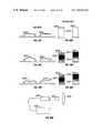
- FIG. 1Ais a cross-section of a display substrate incorporating an anti-reflection coating and integrated supplemental lighting.
- FIG. 1Breveals another scheme for supplemental lighting.
- FIG. 2shows detail of the fabrication process of a micromachined arc lamp source.
- FIG. 3illustrates a bias centered driving scheme for arrays of IMods in a display.
- FIG. 4Ais a diagram which illustrates a color display scheme based on the concept of “base+pigment”.
- FIG. 4Breveals a block diagram of a system that provides for field reconfigurable display centric products.
- FIG. 4Cillustrates the concept as applied to a general-purpose display-centric product.
- FIG. 5Ais a diagram revealing an IMod geometry that decouples the optical behavior from the electromechanical behavior, shown in the un-actuated state.
- FIG. 5Bshows the same IMod in the actuated state.
- FIG. 5Cis a plot showing the performance of this IMod design in the black and white state.
- FIG. 5Dis a plot showing the performance of several color states.
- FIG. 6Ashows a diagram of an IMod that similarly decouples the optical behavior from the electromechanical, however the support structure is hidden.
- FIG. 6Bshows the same design in the actuated state.
- FIG. 7Aillustrates an IMod design that utilizes anisotropically stressed membranes, in one state.
- FIG. 7Bshows the same IMod in another state.
- FIG. 8Ais an illustration showing an IMod that relies on rotational actuation.
- FIG. 8Breveals the fabrication sequence of the rotational IMod design.
- FIG. 9Ais a block diagram of a MEMS switch.
- FIG. 9Bis a block diagram of a row driver based on MEMS switches.
- FIG. 9Cis a block diagram of a column driver based on MEMS switches.
- FIG. 9Dis a block diagram of a NAND gate based on MEMS switches.
- FIG. 9Eis a block diagram of a display system incorporating MEMS based logic and driver components.
- FIG. 10A-10Hshow the structure, fabrication, and operation of a MEMS switch.
- FIG. 10Iillustrates an alternative switch design.
- FIG. 10Jillustrates a second alternative switch design.
- FIG. 11Ais a drawing that shows examples of microring based 2-D photonic structure.
- FIG. 11Bis a drawing of a periodic 2-D photonic structure.
- FIG. 12is a diagram which revealing an example of a 3-D photonic structure.
- FIG. 13Ais a drawing illustrating an IMod incorporating a microring structure in the un-actuated state.
- FIG. 13Bis the same IMod in the actuated state.
- FIG. 13Cshows an IMod incorporating periodic 2-D photonic structure.
- FIG. 14Aillustrates and IMod design which acts as an optical switch.
- FIG. 14Bshows a variation of this design that acts as an optical attenuator.
- FIG. 15Ais a diagram of an IMod design that functions as an optical switch or optical decoupler.
- FIG. 15Billustrates how combinations of these IMods can act as a NXN optical switch.
- FIG. 16shows the fabrication sequence for a tunable IMod structure.
- FIG. 17Aillustrates how the tunable IMod structure can be incorporated into a wavelength selective switch.
- FIG. 17Bfurther illustrates how the wavelength selective switch may incorporate solid state devices.
- FIG. 17Cillustrates how bump-bonded components may be intergrated.
- FIG. 18Ais a schematic representation of a two-channel equalizer/mixer.
- FIG. 18Billustrates how the equalizer/mixer may be implemented using IMod based components.
- FIG. 19is a diagram illustrating a continuous web-based fabrication process.
- FIG. 20A-20Gillustrates how IMod based test structures may be used as tools for stress measurement.
- FIGS. 21A-21Eillustrate various types of discontinuous films which can be used an IMod structure.
- IMod designAn attribute of one previously described IMod design (the induced absorber design described in U.S. patent application Ser. No. 08/554,630, filed on Nov. 6, 1995, and incorporated by reference) is the efficiency of its dark state, in which it can absorb as much as 99.7% of light which is incident upon it. This is useful in reflective displays.
- the IModreflects light of a certain color in the un-actuated state, and absorbs light in the actuated state.
- the IMod arrayresides on a substrate, the potential for absorption is diminished by the inherent reflection of the substrate. In the case of a glass substrate, the amount of reflection is generally about 4% across the visible spectrum. Thus, despite the absorptive capability of the IMod structure, a dark state can only be as dark as the front surface reflection from the substrate will permit.
- AR coatingsanti-reflection coatings
- These coatingscan comprise one or more layers of dielectric films deposited on the surface of a substrate and are designed to reduce the reflection from that surface.
- dielectric filmsdeposited on the surface of a substrate and are designed to reduce the reflection from that surface.
- There are many different possible configurations for such films and design and fabricationis a well known art.
- One simple film designis a single coating of magnesium fluoride approximately one-quarter wave thick.
- Another exampleutilizes a quarter wave film of lead fluoride deposited on the glass, followed by a quarter wave film of magnesium fluoride, with yet a third example interposing a film of zinc sulfide between the two.
- FIG. 1Aillustrates one way in which an AR coating may be incorporated into an IMod display to improve the performance of the display system.
- AR coating 100which, as stated, could comprise one or more thin films, is deposited on the surface of glass layer 102 bonded to glass substrate 106 , on the opposite side of which is fabricated IMod array 108 .
- the presence of AR coating 100reduces the amount of incident light 109 reflected from the surface by coupling more of it into the glass layer 102 . The result is that more of the incident light is acted upon by the IMod array and a darker display state can be obtained when the IMod is operating in the absorptive mode.
- the AR coating 100could also be deposited directly on the surface of glass substrate 106 on the side opposite that of the IMod array.
- FIG. 1Aalso shows how supplemental lighting may be supplied to such a display.
- an array of microscopic arc lamps, 104is fabricated into glass layer 102 .
- Arc lampsare efficient suppliers of light. Historically, arc lamps have been fabricated using techniques relevant to the fabrication of ordinary light bulbs. A typical version of such a lamp is described in U.S. Pat. No. 4,987,496. A glass vessel is built, and electrodes, fabricated separately, are enclosed in the vessel. After filling with an appropriate gas, the vessel is sealed. Although such bulbs may be made small, their method of manufacture may not be suited to the fabrication of large monolithic arrays of such bulbs.
- micromechanical structuresmay be applied to the fabrication of microscopic discharge or arc lamps. Because of the microscopic size of these “micro-lamps”, the voltages and currents to drive them are significantly lower than those required to supply arc lamps fabricated using conventional means and sizes.
- the arrayis fabricated such that light 113 emitted by the lamps is directed towards the IMod array 108 by an inherent reflector layer 111 , which is described below.
- FIG. 2provides detail on how one such lamp, optimized for a flat panel display, could be fabricated.
- the sequenceis described as follows.
- glass layer 200is etched to form a reflector bowl 201 using wet or dry chemical etching.
- the depth and shape of the bowlare determined by the required area of illumination for each lamp.
- a shallow bowlwould produce a broad reflected beam spread while a parabola would tend to collimate the reflected light.
- the diameter of the bowlcould vary from 10 to several hundred microns. This dimension is determined by the amount of display area that can be acceptably obscured from the viewer's perspective. It is also a function of the density of the array of micro-lamps.
- a reflector/metal halide layer 204 and sacrificial layer 202are deposited and patterned.
- the reflector/metal halide layercould be a film stack comprising aluminum (the reflector) and metal halides such as thallium iodide, potassium iodide, and indium iodide.
- the metal halidewhile not essential, can enhance the properties of the light that is generated.
- the sacrificial layercould be a layer such as silicon, for example.
- electrode layer 206is deposited and patterned to form two separate electrodes.
- This materialcould be a refractory metal like tungsten and would have a thickness that is sufficient to provide mechanical support, on the order of several thousand angstroms.
- sacrificial layer 202is removed using a dry release technique.
- the assembly(in the form of an array of such lamps) is sealed by bonding to a glass plate like substrate 106 (shown in FIG. 1A ) such that the reflector faces the plate.
- a gas, such as xenonis used to backfill the cavities, formed by the lamps during the sealing process, to a pressure of approximately one atmosphere. This could be accomplished by performing the sealing process in an airtight chamber that has been previously filled with Xenon.
- the application of sufficient voltage to the electrodes of each lampwill result in an electrical discharge, in the gas between the ends of the electrodes, and the emission of light 205 in a direction away from the reflector 204 .
- This voltagecould be as low as several tens of volts if the gap spacing is on the order of several hundred microns or less.
- the sacrificial layer, 202will determine the position of the electrodes within the bowl. In this case, the thickness is chosen to position the discharge at the focal point of the bowl. Should there be residual stress, which would cause the electrodes to move when released, then thickness is chosen to compensate for this movement. In general the thickness will be some fraction of the depth of the bowl, from several to tens of microns.
- the lightis shown traveling along a path 113 .
- lightis emitted towards the IMod array, where it is acted on and subsequently reflected by the array along paths 110 , towards interface 107 and the viewer 111 .
- the lampsmay be fabricated without including the reflector layer so that they may emit light omnidirectionally.
- Lamps fabricated with or without the reflectormay be used in a variety of applications requiring microscopic light sources or light source arrays. These could include projection displays, backlights for emissive flat panel displays, or ordinary light sources for internal (homes, buildings) or external (automobiles, flashlights) use.
- Light guide 118comprises a glass or plastic layer that has been bonded to substrate 112 .
- Light source 116which could comprise any number of emissive sources such as fluorescent tubes, LED arrays, or the aforementioned micro-lamp arrays, is mounted on opposite sides of the light guide.
- the light 122is coupled into the light guide using a collimator 120 such that most of the light is trapped within the guide via total internal reflection.
- Scatter pad 124is an area of the light guide that has been roughened using wet or dry chemical means.
- the scatter padis coated with a material or thin film stack 126 which presents a reflective surface towards substrate 112 and an absorbing surface towards the viewer 128 .
- the scatter padsare fabricated in an array, with each pad dimensioned such that the portion of the display that it obscures from direct view is hardly noticeable. While these dimensions are small, on the order of tens of microns, they can provide sufficient supplemental lighting because of the inherent optical efficiency of the underlying IMod array 114 .
- the shape of the scatter padmay be circular, rectangular, or of arbitrary shapes which may minimize their perception by the viewer.
- a sequence of voltagesis applied to the rows and columns of the array in what is generally known as a “line at a time” fashion.
- the basic conceptis to apply a sufficient voltage to a particular row such that voltages applied to selected columns cause corresponding elements on the selected row to actuate or release depending on the column voltage.
- the thresholds and applied voltagesmust be such that only the elements on the selected row are affected by the application of the column voltages.
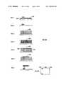
- Hysteresis curve 300is an idealized representation of the electroptical response of a reflective IMod.
- the x-axisshows applied voltage, and the y-axis shows amplitude of reflected light.
- the IModexhibits hysteresis because, as the voltage is increased past the pull-in threshold, the IMod structure actuates and becomes highly absorbing. When the applied voltage is decreased, the applied voltage must be brought below the release threshold in order for the structure to move back into the un-actuated state. The difference between the pull-in and release thresholds produces the hysteresis window.
- the hysteresis effectas well as an alternative addressing scheme, is discussed in U.S.
- timing diagram 302illustrates the kind of waveforms that may be applied to actuate an array of IMods that exhibit a hysteresis curve resembling curve 300 .
- a total of five voltages, two column voltages and three row voltages,are required.
- the voltagesare selected such that Vcol 1 is exactly twice the value of Vbias, and Vcol 0 is zero volts.
- the row voltagesare selected so that the difference between Vsel F 0 and Vcol 0 equals Von, and the difference between Vsel F 0 and Vcol 1 equals Voff. Conversely, the difference between Vsel F 1 and Vcol 1 equals Von, and the difference between Vsel F 1 and Vcol 0 equals Voff.
- the addressingoccurs in alternating frames 0 and 1 .
- data for row 0is loaded into the column drivers during frame 0 resulting in either a voltage level of Vcol 1 or Vcol 0 being applied depending on whether the data is a binary one or zero respectively.
- row driver 0applies a select pulse with the value of Vsel F 0 . This results in any IMods on columns with Vcol 0 present becoming actuated, and IMods on columns with Vcol 1 present, releasing.
- the data for the next rowis loaded into the columns and a select pulse applied to that row and so on sequentially until the end of the display is reached. Addressing is then begun again with row 0 ; however this time the addressing occurs within frame 1 .
- the difference between the framesis that the correspondence between data and column voltages is switched, a binary zero is now represented by Vcol 0 , and the row select pulse is now at the level of Vsel F 1 .
- the overall polarity of the voltages applied to the display arrayis alternated with each frame. This is useful, especially for MEMS based displays, because it allows for the compensation of any DC level charge buildup that can occur when only voltages of a single polarity are applied.
- the buildup of a charge within the structurecan significantly offset the electroptical curve of the IMod or other MEM device.
- the IModis a versatile device with a variety of potential optical responses, a number of different color display schemes are enabled having different attributes.
- One potential schemeexploits the fact that there are binary IMod designs that are capable of achieving color states, black states, and white states in the same IMod. This capability can be used to achieve a color scheme that can be described as “base+pigment”. This terminology is used because the approach is analogous to the way in which paint colors are produced by adding pigments to a white base to achieve a desired color. Using this approach, a particular paint can attain any color in the spectrum and any level of saturation by controlling the content and amount of pigments that are added to the base. The same can be said for a display that incorporates colored and black and white pixels.
- a pixel 400comprises five subpixel elements, 402 , 404 , 406 , and 408 , with each subpixel capable of reflecting red, green, blue, and white respectively. All of the subpixels are capable of a black state. Control over the brightness of each subpixel can be accomplished using pulse width modulation related techniques as discussed in U.S. Pat. No. 5,835,255. In conjunction with properly selected relative subpixel sizes, this results in a pixel over which a very large degree of control can be exercised of brightness and saturation. For example, by minimizing the overall brightness of the white subpixels, highly saturated colors may be achieved. Conversely, by minimizing the brightness of the color subpixels, or by maximizing them in conjunction with the white subpixels, a bright black and white mode may be achieved. All variations in between are obviously attainable as well.
- a usermay want to use a product in black and white mode if, some context, only text were being viewed. In another situation, however, the user may want to view high quality color still images, or in yet another mode may want to view live video.
- Each of these modeswhile potentially within the range of a given IMod display configuration, requires tradeoffs in particular attributes. Tradeoffs include the need for low refresh rates if high-resolution imagery is required, or the ability to achieve high gray scale depth if only black and white is requested.
- the controller hardwaremay be reconfigurable to some extent. Tradeoffs are a consequence of the fact that any display has only a certain amount of bandwidth, which is fundamentally limited by the response time of the pixel elements and thus determines the amount of information which can be displayed at a given time.
- controller logic 412is implemented using one of a variety of IC technologies, including programmable logic devices (PLAs) and field programmable gate arrays (FPGAs), which allow for the functionality of the component to be altered or reconfigured after it leaves the factory.
- PLAsprogrammable logic devices
- FPGAsfield programmable gate arrays
- Such deviceswhich are traditionally used for specialized applications such as digital signal processing or image compression, can provide the high performance necessary for such processing, while supplying flexibility during the design stage of products incorporating such devices.
- the controller 412provides signals and data to the driver electronics 414 and 416 for addressing the display 418 .
- Conventional controllersare based on IC's or Application Specific Integrated Circuits (ASICs), which are effectively “programmed” by virtue of their design during manufacture.
- the term programin this case, means an internal chip layout comprising numerous basic and higher level logical components (logic gates and logic modules or assemblies of gates).
- field programmable devicessuch PLAs or FPGAs, different display configurations may be loaded into the display controller component in the form of hardware applications or “hardapps”, from a component 410 , which could be memory or a conventional microprocessor and memory.
- the memorycould be in the form of EEPROMS or other reprogrammable storage devices, and the microprocessor could take on the form of simple microcontroller whose function is to load the hardapp from memory into the FPGA, unless this were performed by whatever processor is associated with the general functioning of the product.
- This approachis advantageous because with relatively simple circuitry it is possible to achieve a wide variety of different display performance configurations and mixed display scan rates, along with the potential to combine them.
- One portion of the screenfor example, might be operated as a low-resolution text entry area, while another provides high quality rendition of an incoming email. This could be accomplished, within the overall bandwidth limitations of the display, by varying the refresh rate and # of scans for different segments of the display.
- the low-resolution text areacould be scanned rapidly and only once or twice corresponding to one or two bits of gray scale depth.
- the high rendition email areacould be scanned rapidly and with three or four passes corresponding to three or four bits of grayscale.
- FIG. 4Cshows a configuration of a generic portable electronic product 418 that has a programmable logic device or equivalent at its core 420 .
- the central processoris a variant of a RISC processor that uses a reduced instruction set. While RISC processors are more efficient versions of CPUs that power most personal computers, they are still general-purpose processors that expend a lot of energy performing repetitive tasks such as retrieving instructions from memory.
- the hardapp processor 420is shown at the center of a collection of I/O devices and peripherals that it will utilize, modify, or ignore based on the nature and function of the hardapp currently loaded.
- the hardappscan be loaded from memory 422 resident in the product, or from an external source via RF or IR interface, 424 , which could pull hardapps from the internet, cellular networks, or other electronic devices, along with content for a particular hardapp application.
- Other examples of hardappsinclude voice recognition or speech synthesis algorithms for the audio interface 432 , handwriting recognition algorithms for pen input 426 , and image compression and processing modes for image input device 430 .
- Such a productcould perform a myriad of functions by virtue of its major components, the display as the primary user interface and the reconfigurable core processor. Total power consumption for such a device could be on the order of tens of milliwatts versus the several hundred milliwatts consumed by existing products.
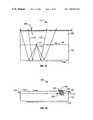
- FIGS. 5A and 5BAnother way in which this may be accomplished is illustrated in FIGS. 5A and 5B .
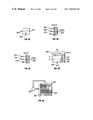
- This designuses electrostatic forces to alter the geometry of an interferometric cavity.
- Electrode 502is fabricated on substrate 500 and electrically isolated from membrane/mirror 506 by insulating film 504 . Electrode 502 functions only as an electrode, not also as a mirror.
- An optical cavity 505is formed between membrane/mirror 506 and secondary mirror 508 .
- Support for secondary mirror 508is provided by a transparent superstructure 510 , which can be a thick deposited organic, such as SU- 8 , polyimide, or an inorganic material.
- the membrane/mirror 506With no voltage applied, the membrane/mirror 506 , maintains a certain position shown in FIG. 5A , relative to secondary mirror 508 , as determined by the thickness of the sacrificial layers deposited during manufacture. For an actuation voltage of about four volts a thickness of several thousand angstroms might be appropriate.
- the secondary mirroris made from a suitable material, say chromium, and the mirror/membrane made from a reflective material such as aluminum, then the structure will reflect certain frequencies of light 511 which may be perceived by viewer 512 .
- the chromiumis thin enough to be semitransparent, about 40 angstroms, and the aluminum sufficiently thick, at least 500 angstroms, as to be opaque, then the structure may have a wide variety of optical responses.
- FIGS. 5C and 5Dshow examples of black and white and color responses respectively, all of which are determined by the cavity length, and the thickness of the constituent layers.
- FIG. 5Bshows the result of a voltage applied between primary electrode 502 and membrane mirror 506 .
- the membrane/mirroris vertically displaced thus changing the length of the optical cavity and therefore the optical properties of the IMod.
- FIG. SCshows one kind of reflective optical response which is possible with the two states, illustrating the black state 521 when the device is fully actuated, and a white state 523 when the device is not.
- FIG. 5Dshows an optical response with color peaks 525 , 527 , and 529 , corresponding to the colors blue, green, and red respectively.
- the electromechanical behavior of the devicethus may be controlled independently of the optical performance.
- Materials and configuration of the primary electrode, which influence the electromechanics,may be selected independently of the materials comprising the secondary mirror, because they play no role in the optical performance of the IMod.
- This designmay be fabricated using processes and techniques of surface micromachining, for example, the ones described in U.S. patent application Ser. No. 08,688,710, filed on Jul. 31, 1996 and incorporated by reference.
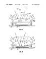
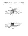
- the support structure for the IMod 606is positioned to be hidden by the membrane/mirror 608 .
- the amount of inactive areais effectively reduced because the viewer sees only the area covered by the membrane/mirror and the minimum space between adjoining IMods. This is unlike the structure in FIG. 5A where the membrane supports are visible and constitute inactive and inaccurate, from a color standpoint, area.
- FIG. 6Breveals the same structure in the actuated state.
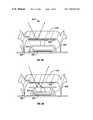
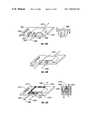
- FIG. 7Aanother geometric configuration is illustrated for use in an IMod structure.
- This designis similar to one shown in U.S. Pat. No. 5,638,084. That design relied upon an opaque plastic membrane that is anisotropically stressed so that it naturally resides in a curled state. Application of a voltage flattens the membrane to provide a MEMS-based light shutter.
- the device's functionalitymay be improved by making it interferometric.
- the IMod variationis shown in FIG. 7A where thin film stack 704 is like the dielectric/conductor/insulator stack which is the basis for the induced absorber IMod design discussed in U.S. patent application Ser. No. 08/688,710, filed on Jul. 31, 1996 and incorporated by reference.
- Aluminum 702which could also include other reflective metals (silver, copper, nickel), or dielectrics or organic materials which have been undercoated with a reflective metal, is deposited on a thin sacrificial layer so that it may be released, using wet etch or gas phase release techniques.
- Aluminum membrane 702is further mechanically secured to the substrate by a support tab 716 , which is deposited directly on optical stack 704 . Because of this, light that is incident on the area where the tab and the stack overlap is absorbed making this mechanically inactive area optically inactive as well. This technique eliminates the need for a separate black mask in this and other IMod designs.
- Incident light 706is either completely absorbed or a particular frequency of light 708 , is reflected depending on the spacing of the layers of the stack.
- the optical behavioris like that of the induced absorber IMod described in U.S. patent application Ser. No. 08/688,710, filed on Jul. 31, 1996, and incorporated by reference.
- FIG. 7Bshows the device configuration when no voltage is applied.
- the residual stresses in the membraneinduce it to curl up into a tightly wound coil.
- the residual stressescan be imparted by deposition of a thin layer of material 718 on top of the membrane, which has extremely high residual tensile stress. Chromium is one example in which high stresses may be achieved with a film thickness a low as several hundred angstroms.
- light beam 706is allowed to pass through the stack 704 and intersect with plate 710 .
- Plate 710can reside in a state of being either highly absorbing or highly reflective (of a particular color or white).
- the optical stack 704would be designed such that when the device is actuated it would either reflect a particular color (if plate 710 were absorbing) or be absorbing (if plate, 710 were reflective).
- IMod geometryrelies on rotational actuation.
- electrode 802an aluminum film about 1000 angstroms thick, is fabricated on substrate 800 .
- Support post 808 and rotational hinge 810support shutter 812 , upon which a set of reflecting films 813 has been deposited.
- the support shuttermay be an aluminum film which is several thousand angstroms thick. Its X-Y dimensions could be on the order of tens to several hundred microns.
- the filmsmay be interferometric and designed to reflect particular colors.
- a fixed interferometric stack in the form of an induced absorber like that described in U.S. patent application Ser. No. 08/688,710, filed on Jul. 31, 1996 and incorporated by referencewould suffice. They may also comprise polymers infused with color pigments, or they may be aluminum or silver to provide broadband reflection.
- the electrode 802 and the shutter 812are designed such that the application of a voltage (e.g., 10 volts) between the two causes the shutter 812 to experience partial or full rotation about the axis of the hinge. Only shutter 818 is shown in a rotated state although typically all of the shutters for a given pixel would be driven in unison by a signal on the common bus electrode 804 .
- Such a shutterwould experience a form of electromechanical hysteresis if the hinges and electrode distances were designed such that the electrostatic attraction of the electrodes overcomes the spring tension of the hinge at some point during the rotation.
- the shutterswould thus have two electromechanically stable states.
- FIG. 8Aillustrates the reflective mode where incident light 822 is reflected back to the viewer 820 .
- the shuttereither reflects a white light, if the shutter is metallized, or reflects a particular color or set of colors, if it is coated with interferometric films or pigments. Representative thicknesses and resulting colors, for an interferometric stack, are also described in U.S. patent application Ser. No. 08/688,710, filed on Jul. 31, 1996 and incorporated by reference.
- the lightis allowed to pass through and be absorbed in substrate 800 if the opposite side of the shutter were coated with an absorbing film or films 722 .
- These filmscould comprise another pigment infused organic film, or an induced absorber stack designed to be absorbing.
- the shuttersmay be highly absorbing, i.e., black, and the opposite side of substrate 800 coated with highly reflective films 824 , or be selectively coated with pigment or interferometric films to reflect colors, along the lines of the color reflecting films described above.
- supplementary electrode 814which provides additional torque to the shutter when charged to a potential that induces electrostatic attraction between supplementary electrode 814 and shutter 812 .
- Supplementary electrode 814comprises a combination of a conductor 814 and support structure 816 .
- the electrodemay comprise a transparent conductor such as ITO that could be about thousand angstroms thick. All of the structures and associated electrodes are machined from materials that are deposited on the surface of a single substrate, i.e. monolithically, and therefore are easily fabricated and reliably actuated due to good control over electrode gap spaces.
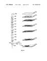
- FIG. 8Bshows a fabrication sequence for the rotational modulator.
- substrate 830has been coated with electrode 832 and insulator 834 .
- Typical electrode and insulator materialsare aluminum and silicon dioxide, each of a thickness of one thousand angstroms each. These are patterned in step 2 .
- Sacrificial spacer 836a material such as silicon several microns in thickness, has been deposited and patterned in step 3 and coated with post/hinge/shutter material 838 in step 4 . This could be an aluminum alloy or titanium/tungsten alloy about 1000 angstroms thick.
- material 838has been patterned to form bus electrode 844 , support post 840 , and shutter 842 .
- Shutter reflector 846has been deposited and patterned in step 6 .
- the sacrificial spacerhas been etched away yielding the completed structure.
- Step 7also reveals a top view of the structure showing detail of the hinge comprising support posts 848 , torsion arm 850 , and shutter 852 .
- IModsthat are binary devices only a small number of voltage levels is required to address a display.
- the driver electronicsneed not generate analog signals that would be required to achieve gray scale operation.
- the electronicsmay be implemented using other means as suggested in U.S. patent application Ser. No. 08/769,947, filed on Dec. 19, 1996 and incorporated by reference.
- the drive electronics and logic functionscan be implemented using switch elements based on MEMS.
- FIGS. 9A through 9Eillustrate the concept.
- FIG. 9Ais a diagram of a basic switch building block with an input 900 making a connection to output 904 by application of a control signal 902 .
- FIG. 9Billustrates how a row driver could be implemented.
- the row driver for the addressing scheme described aboverequires the output of three voltage levels.
- Application of the appropriate control signals to the row driverallows one of the input voltage levels to be selected for output 903 .
- the input voltagesare Vcol 1 , Vcol 0 , and Vbias corresponding to 906 , 908 , and 910 in the figure.
- the appropriate control signalsresult in the selection of one or the other input voltage levels for delivery to the output 920 .
- FIG. 9Dillustrates how a logic device 932 , may be implemented, in this case a NAND gate, using basic switch building blocks 934 , 936 , 938 , and 940 . All of these components can be configured and combined in a way that allows for the fabrication of the display subsystem shown in FIG. 9 E.
- the subsystemcomprises controller logic 926 , row driver 924 , column driver 928 , and display array 930 , and uses the addressing scheme described above in FIG. 3 .
- the switch fabrication processbecomes a subprocess of the IMod fabrication process and is illustrated in FIG. 10A-10H .
- FIGS. 10A and 10Bthe initial stage of the IMods fabrication process is shown, FIG. 10 A.
- Arrow 1004indicates the direction of the perspective of the side view.
- Substrate 1000has had sacrificial spacer 1002 a silicon layer 2000 angstrom thick deposited and patterned on its surface.
- a structural materialan aluminum alloy several microns thicks, has been deposited and patterned to form a source beam 1010 , drain structure 1008 , and gate structure 1006 .
- a non-corroding metalsuch as gold, irridium or platinum may be plated onto the structural material at this point to maintain low contact resistance through the life of the switch.
- Notch 1012has been etched in source beam 1010 to facilitate the movement of the beam in a plane parallel to that of the substrate.
- Arrows 1016indicate the direction of the perspective front view.
- the sacrificial material 1002has been etched away leaving the source beam 1010 intact and free to move.
- Step 1shows both a side view and top view of the initial stage.
- Arrow 1004indicates the direction of the perspective of the side view.
- Substrate 1000has had sacrificial spacer 1002 a silicon layer 2000 angstroms thick deposited and patterned on its surface.
- a structural materialan aluminum alloy several microns thick, has been deposited and patterned to form source beam 1010 , drain structure 1008 , and gate structure 1006 .
- Several hundred angstroms of a non-corroding metalsuch as gold, iridium or platinum may be plated onto the structural material at this point to maintain low contact resistance through the life of the switch.
- Notch 1012has been etched in source beam 1010 to facilitate the movement of the beam in a plane parallel to that of the substrate.
- step 3The perspective of the drawing is different in steps 3 and 4 , which now compare a front view with a top view. Arrows 1016 indicate the direction of the perspective of the front view.
- step 3the sacrificial material has been etched away leaving the source beam 1010 intact and free to move.
- the source beam 1010when the voltage is applied between the source beam and the gate structure, the source beam 1010 is deflected towards gate 1006 until it comes into contact with the drain 1008 , thereby establishing electrical contact between the source and the drain.
- the mode of actuationis parallel to the surface of the substrate, thus permitting a fabrication process that is compatible with the main IMod fabrication processes. This process also requires fewer steps than those used to fabricate switches that actuate in a direction normal the substance surface.
- FIGS. 10I and 10Jillustrate two alternative designs for planar MEM switches.
- the switch in FIG. 10Idiffers in that switch beam 1028 serves to provide contact between drain 1024 and source 1026 .
- currents that must pass through the source beam to the drainmay effect switching thresholds, complicating the design of circuits. This is not the case with switch 1020 .
- the switch in FIG. 10Jreveals a further enhancement.
- insulator 1040electrically isolates switch beam 1042 from contact beam 1038 .
- This insulatormay be a material such as SiO 2 that can be deposited and patterned using conventional techniques. Use of such a switch eliminates the need to electrically isolate switch drive voltages from logic signals in circuits comprising these switches.
- IModsfeature elements that have useful optical properties and are movable by actuation means with respect to themselves or other electrical, mechanical or optical elements.
- Assemblies of thin films to produce interferometric stacksare a subset of a larger class of structures that we shall refer to as multidimensional photonic structures.
- a photonic structureas one that has the ability to modify the propagation of electromagnetic waves due to the geometry and associated changes in the refractive index of the structure. Such structures have a dimensional aspect because they interact with light primarily along one or more axes. Structures that are multidimensional have also been referred to as photonic bandgap structures (PBG's) or photonic crystals.
- PBG'sphotonic bandgap structures
- the text “Photonic Crystals” by John D. Joannopoulos, et aldescribes photonic structures that are periodic.
- a one-dimensional PBGcan occur in the form of a thin film stack.
- FIG. 16shows the fabrication and end product of an IMod in the form of a dielectric Fabry-Perot filter.
- Thin film stacks 1614 and 1618which could be alternating layers of silicon and silicon dioxide each a quarter wave thick, have been fabricated on a substrate to form an IMod structure that incorporates central cavity 1616 .
- the stackis continuous in the X and Y direction, but has a periodicity in the optical sense in the Z direction due to variations in the refractive index of the material as they are comprised of alternating layers with high and low indices.
- This structurecan be considered one-dimensional because the effect of the periodicity is maximized for waves propagating along one axis, in this case the Z-axis.
- FIGS. 11A and 11Billustrate two manifestations of a two-dimensional photonic structure.
- a microring resonator 1102can be fabricated from one of a large number of well known materials, an alloy of tantalum pentoxide and silicon dioxide for example, using well known techniques.
- the structureis essentially a circular waveguide whose refractive index and dimensions w, r, and h determine the frequencies and modes of light which will propagate within it.
- a resonatorif designed correctly, can act as a frequency selective filter for broadband radiation that is coupled into it. In this case, the radiation is generally propagating in the XY plane as indicated by orientation symbol 1101 .
- the one-dimensional analog of this devicewould be a Fabry-Perot filter made using single layer mirrors. Neither device exhibits a high order optical periodicity, due to the single layer “boundaries” (i.e. mirrors); however, they can be considered photonic structures in the broad sense.
- FIG. 11 BA more traditional PBG is shown in FIG. 11 B.
- Columnar array 1106presents a periodic variation in refractive index in both the X and Y directions. Electromagnetic radiation propagating through this medium is most significantly affected if it is propagating within the XY plane, indicated by orientation symbol 1103 .
- the array of FIG. 11Bshares attributes with a one-dimensional thin film stack, except for its higher-order dimensionality.
- the arrayis periodic in the sense that along some axis through the array, within the XY plane, the index of refraction varies between that of the column material, and that of the surrounding material, which is usually air.
- Appropriate design of this arrayutilizing variations on the same principles applied to the design of thin film stacks, allows for the fabrication of a wide variety of optical responses, (mirrors, bandpass filters, edge filters, etc.) acting on radiation traveling in the XY plane.
- Array 1106in the case shown in FIG.
- 11Bincludes a singularity or defect 1108 in the form of a column that differs in its dimension and/or refractive index.
- the diameter of this columnmight be fractionally larger or smaller than the remaining columns (which could be on the order of a quarter wavelength in diameter), or it may be of a different material (perhaps air vs. silicon dioxide).
- the overall size of the arrayis determined by the size of the optical system or component that needs to be manipulated.
- the defectmay also occur in the form of the absence of a column or columns (a row), depending on the desired behavior.
- This structureis analogous to the dielectric Fabry-Perot filter of FIG. 16 , but it functions in only two dimensions. In this case, the defect is analogous to the cavity, 1616 .
- the remaining columnsare analogous to the adjacent two-dimensional stacks.
- column x spacing sxthe relevant dimensions of the structure of FIG. 11B are denoted by column x spacing sx, column y spacing sy, (either of which could be considered the lattice constant), column diameter d, and array height, h.
- column diameters and spacingscan be on the order of a quarter wave.
- the height, his determined by the desired propagation modes, with little more than one half wavelength used for single mode propagation.
- the equations for relating the size of the structures to their effect on lightare well known and documented in the text “Photonic Crystals” by John D. Joannopoulos, et al.
- This kind of structuremay also be fabricated using the same materials and techniques used to fabricate the resonator 1102 .
- a single film of siliconmay be deposited on a glass substrate and patterned, using conventional techniques, and etched using reactive ion etching to produce the high aspect ratio columns.
- the diameter and spacing of the columnscould be on the order of 0.5 um and 0.1 um respectively.
- Photonic structuresalso make it possible to direct radiation under restrictive geometric constraints. Thus they are quite useful in applications where it is desirable to redirect and/or select certain frequencies or bands of frequencies of light when dimensional constraints are very tight.
- Waveguideschanneling light propagating in the XY plane, may be fabricated which can force light to make 90 degree turns in a space less than the wavelength of the light. This can be accomplished, for example, by creating the column defect in the form of a linear row, which can act as the waveguide.
- Three-dimensional periodic structure 1202acts on radiation propagating in the XY, YZ , and XZ planes.
- a variety of optical responsesmay be attained by appropriate design of the structure and selection of its constituent materials. The same design rules apply, however they are applied three-dimensionally here.
- Defectsoccur in the form of points, lines, or regions, vs. points and lines, which differ in size and/or refractive index from the surrounding medium.
- the defect 1204is a single point element but may also be linear or a combination of linear and point elements or regions.
- a “linear” or “serpentine” array of point defectsmay be fabricated such that it follows an arbitrary three-dimensional path through the PBG, and acts as a tightly constrained waveguide for light propagating within it.
- the defectwould generally be located internally but is shown on the surface for purposes of illustration. The relevant dimensions of this structure are all illustrated in the figure.
- the diameter and spacing and materials of the PBGare completely application dependent, however the aforementioned design rules and equations also apply.
- Three-dimensional PBGsare more complicated to make.
- Fabrication techniques for building periodic three-dimensional structuresinclude: holographic, where a photosensitive material is exposed to a standing wave and replicates the wave in the form of index variations in the material itself; self-organizing organic or self-assembling materials that rely on innate adhesion and orientation properties of certain co-polymeric materials to create arrays of columnar or spherical structures during the deposition of the material; ceramic approaches that can involve the incorporation of a supply of spherical structures of controlled dimensions into a liquid suspension that, once solidified, organizes the structures, and can be removed by dissolution or high temperature; combinations of these approaches; and others.
- Co-polymeric self-assembly techniquesare especially interesting because they are both low temperature and require minimal or no photolithography.
- this techniqueinvolves the dissolution of a polymer, polyphenylquinoine-block-polystyrene (PPQmPSn) is one example, into a solvent such as carbon disulfide. After spreading the solution onto a substrate and allowing the solvent to evaporate, a close packed hexagonal arrangement of air filled polymeric spheres results. The process can be repeated multiple times to produce multi-layers, the period of the array may be controlled by manipulating the number of repeat units of the components (m and n) of the polymer. Introduction of a nanometer sized colloid comprising metals, oxides, or semiconductors that can have the effect of reducing the period of the array further, as well as increasing the refractive index of the polymer.
- Defectsmay be introduced via direct manipulation of the material on a submicron scale using such tools as focused ion beams or atomic force microscopes.
- the formermay be used to remove or add material in very small selected areas or to alter the optical properties of the material.
- Material removaloccurs when the energetic particle beam, such as that used by a Focused Ion Beam tool, sputters away material in its path.
- Material additionoccurs when the focused ion beam is passed through a volatile metal containing gas such as tungsten hexafluoride (for tungsten conductor) or silicon tetrafluoride (for insulating silicon dioxide). The gas breaks down, and the constituents are deposited where the beam contacts the substrate.
- Atomic force microscopymay be used to move materials around on the molecular scale.
- micro-electrodepositionAnother approach involves the use of a technique that can be called micro-electrodeposition and which is described in detail in U.S. Pat. No. 5,641,391.
- a single microscopic electrodecan be used to define three-dimensional features of submicron resolution using a variety of materials and substrates.
- Metal “defects” deposited in this waycould be subsequently oxidized to form an dielectric defect around which the PBG array could be fabricated using the techniques described above.
- the existence of surface features, in the form of patterns of other materials, on the substrate upon which the PBG is fabricatedmay also serve as a template for the generation of defects within the PBG during its formation. This is particularly relevant to PBG processes that are sensitive to substrate conditions, primarily self-assembly approaches. These features may encourage or inhibit the “growth” of the PBG in a highly localized region around the seed depending on the specific nature of the process. In this way, a pattern of defect “seeds” may be produced and the PBG formed afterwards with the defects created within during the PBG formation process.
- the class of devices known as IModsmay be further broadened by incorporating the larger family of multidimensional photonic structures into the modulator itself.
- Any kind of photonic structure, which is inherently a static device,may now be made dynamic by altering its geometry and/or altering its proximity to other structures.
- the micromechanical Fabry-Perot filtershown in FIG. 16 , comprising two mirrors which are each one-dimensional photonic structures, may be tuned by altering the cavity width electrostatically.
- FIG. 13shows two examples of IMod designs incorporating two-dimensional PBGs.
- a cutaway diagramreveals a self-supporting membrane 1304 , which has been fabricated with a microring resonator 1306 mounted on the side facing the substrate.
- Waveguides 1301 and 1302 lying within the bulk of the substrate 1303are planar and parallel and can be fabricated using known techniques.
- the IModis shown in the un-driven state with a finite airgap (number) between the microring and the substrate.
- the microringis fabricated so that its position overlaps and aligns with the paired waveguides in the substrate below. Dimensions of the microring are identical to the example described above.
- light 1308propagates undisturbed in waveguide 1302 , and the output beam 1310 is spectrally identical to the input 1308 .
- Driving the IMod to force the microring into intimate contact with the substrate and waveguidesalters the optical behavior of the device.
- Light propagating in waveguide 1302may now couple into the microring by the phenomenon of evanescence.
- the microringif sized appropriately, acts as an optical resonator coupling a selected frequency from waveguide 1302 and injecting it into waveguide 1301 .
- FIG. 13Bwhere light beam 1312 is shown propagating in a direction opposite the direction of light 1308 .
- Such a devicemay be used as a frequency selective switch that picks particular wavelengths out of a waveguide by the application of a voltage or other driving means required to bring the structure into intimate contact with the underlying waveguides.
- a static version of this geometryis described in the paper B. E. Little, et al, “Vertically Coupled Microring Resonator Channel Dropping Filter”, IEEE Photonics Technology Letters, vol. 11, no. 2, 1999.
- FIG. 13 CAnother example is illustrated in FIG. 13 C.
- a pair of waveguides 1332 and 1330 and resonator 1314are fabricated on the substrate in the form of a columnar PBG.
- the PBGis a uniform array of columns, with the waveguides defined by removing two rows (one for each waveguide), and the resonator defined by removing two columns.
- Top view 1333provides more detail of the construction of waveguides 1330 and 1332 , and the resonator 1314 . Dimensions are dependent on the wavelength of interest as well as materials used. For a wavelength of 1.55 um, the diameter and spacing of the columns could be on the order of 0.5 um and 1 um respectively.
- the height, hdetermines the propagation modes which will be supported and should be slightly more than half the wavelength if only single modes are to be propagated.
- two isolated columns 1311On the inner surface of the membrane 1315 are fabricated two isolated columns 1311 , which are directed downwards, and have the same dimensions and are of the same material (or optically equivalent) as the columns on the substrate.
- the resonator and columnsare designed to complement each other; there is a corresponding absence of a column in the resonator where the column on the membrane is positioned.
- the IModWhen the IMod is in an undriven state, there is a finite vertical airgap 1312 , of at least several hundred nanometers between the PBG and the membrane columns and therefore no optical interaction occurs.
- the absence of columns in the resonatoract like defects, causing coupling between waveguides 1330 and 1332 .
- the deviceacts as does the one shown in FIG. 13 B and selected frequencies of light propagating along waveguide are now injected into waveguide 1332 , and propagate in the opposite direction in the form of light 1329 .
- a device based on the induced absorberincludes a self-supporting aluminum membrane 1400 , on the order of tens to hundreds of microns square, which is suspended over a stack of materials 1402 comprising a combination of metals and oxides and patterned on transparent substrate.
- the films utilized in the induced absorber modulatordescribed in U.S. patent application Ser. No. 08/688,710, filed on Jul. 31, 1996, and incorporated by reference, could serve this purpose.
- the films on the substratemay also comprise a transparent conductor, such as ITO.
- the structuremay incorporate on its underside a lossy metal film such as molybdenum or tungsten, of several hundred angstroms in thickness.
- the materialsare configured so that in the undriven state the device reflects in a particular wavelength region, but becomes very absorbing when the membrane is driven into contact.
- Side view 1410shows a view of the device looking into the side of the substrate.
- Light beam 1408propagates at some arbitrary angle through the substrate and is incident on IMod 1406 , shown in the un-driven state. Assuming the frequency of the light corresponds with the reflective region of the IMod in the un-driven state, the light is reflected at a complementary angle and propagates away.
- Side view, 1414shows the same IMod in the driven state. Because the device is now very absorbing, the light which is incident upon it is no longer reflected but absorbed by the materials in the IMod's stack.
- the IModmay act as an optical switch for light that is propagating within the substrate upon which it is fabricated.
- the substrateis machined to form surfaces that are highly polished, highly parallel (to within 1/10 of a wavelength of the light of interest), and many times thicker (at least hundreds of microns) than the wavelength of light. This allows the substrate to act as a substrate/waveguide in that light beams propagate in a direction which is, on average, parallel to the substrate but undergo multiple reflections from one surface to another.
- Light waves in such a structureare often referred to as substrate guided waves.
- FIG. 14Bshows a variation on this theme.
- Membrane 1420is patterned such that it is no longer rectangular but is tapered towards one end. While the mechanical spring constant of the structure remains constant along this length, electrode area decreases. Thus the amount of force which can be applied electrostatically is lower at the narrower end of the taper. If a gradually increasing voltage is applied, the membrane will begin to actuate at the wider end first and actuation will progress along arrow 1428 as the voltage increases.
- the IModoperates as an absorbing region whose area depends on the value of the applied voltage.
- Side view 1434shows the effect on a substrate propagating beam when no voltage is applied.
- the corresponding reflective area 1429which shows the IMod from the perspective of the incident beam, shows “footprint” 1431 of the beam superimposed on the reflective area. Since the entire area 1429 is non-absorbing, beam, 1430 , is reflected from IMod 1428 (with minimal losses) in the form of beam 1432 .
- variable optical attenuatormay be created, the response of which is directly related to the value of the applied voltage.
- Support frame 1500is fabricated from a metal, such as aluminum several thousand angstroms in thickness, in such a way that it is electrically connected to mirror 1502 .
- Mirror 1502resides on transparent optical standoff 1501 , which is bonded to support 1500 .
- Mirror 1502may comprise a single metal film or combinations of metals, oxides, and semiconducting films.
- the standoffis fabricated from a material that has the same or higher index of refraction than that of the substrate. This could be SiO2 (same index) or a polymer whose index can be varied.
- the standoffis machined so that the mirror is supported at an angle of 45 degrees. Machining of the standoff can be accomplished using a technique known as analog lithography that relies on a photomask whose features are continuously variable in terms of their optical density. By appropriate variation of this density on a particular feature, three-dimensional shapes can be formed in photoresist that is exposed using this mask. The shape can then be transferred into other materials via reactive ion etching.
- the entire assemblyis suspended over conductor, 1503 , which has been patterned to provide an unobstructed “window” 1505 into the underlying substrate, 1504 . That is to say the bulk of conductor 1503 has been etched away so that window 1505 , comprising bare glass, is exposed.
- the switchlike other IMods, can be actuated to drive the whole assembly into contact with the substrate/waveguide.
- Side view, 1512shows the optical behavior. Beam 1510 is propagating within the substrate at an angle 45 degrees from normal that prevents it from propagating beyond the boundaries of the substrate. This is because 45 degrees is above the angle known as the critical angle, which allows the beam to be reflected with minimal or no losses at the interface 1519 between the substrate and the outside medium by the principle of total internal reflection (TIR).
- TIRtotal internal reflection
- TIRThe principle of TIR depends on Snell's law, but a basic requirement is that the medium outside the substrate have an index of refraction that is lower than that of the substrate.
- side view, 1512the device is shown with the switch 1506 in the un-driven state, and beam 1510 propagating in an unimpeded fashion.
- switch 1506is actuated into contact with the substrate as shown in side view 1514 , the beam's path is altered.
- the standoffhas a refractive index greater than or equal to that of the substrate, the beam no longer undergoes TIR at the interface. The beam propagates out of the substrate into the optical standoff, where it is reflected by the mirror.
- the mirroris angled, at 45 degrees, such that the reflected beam is now traveling at an angle which is normal to the plane of the substrate.
- the resultis that the light may propagate through the substrate interface because it no longer meets the criteria for TIR, and can be captured by a fiber coupler 1520 , which has been mounted on the opposite side of the substrate/waveguide.
- a similar conceptis described in the paper, X. Zhou, et al, “Waveguide Panel Display Using Electromechanical Spatial Modulators”, SID Digest, vol. XXIX, 1998. This particular device was designed for emissive display applications.
- the mirrormay also be implemented in the form of a reflecting grating, which may be etched into the surface of the standoff using conventional patterning techniques.
- optical structuresmay be substituted for the mirror as well with their respective attributes and shortcomings. These can be categorized as refractive, reflective, and diffractive and can include micro-lenses (both transmissive and reflective), concave or convex mirrors, diffractive optical elements, holographic optical elements, prisms, and any other form of optical element which can be created using micro-fabrication techniques. In the case where an alternative optical element is used, the standoff and the angle it imparts to the optic may not be necessary depending on the nature of the micro-optic.
- This variation on the IModacts as a de-coupling switch for light.
- Broadband radiationor specific frequencies if the mirror is designed correctly, can be coupled out of the substrate/waveguide at will.
- Side view 1526shows a more elaborate implementation in which an additional fixed mirror, angled at 45 degrees, has been fabricated on the side of the substrate opposite that of the de-coupling switch. This mirror differs from the switch in that it cannot be actuated. By careful selection of the angles of the mirrors on both structures, light 1522 that has been effectively decoupled out of the substrate by switch 1506 may be re-coupled back into the substrate by re-coupling mirror 1528 .
- the mirror combinationmay be used to redirect light in any new direction within the substrate/waveguide.
- the combination of these two structureswill be referred to as a directional switch.
- Re-coupling mirrorscan also be used to couple any light that is propagating into the substrate in a direction normal to the surface.
- FIG. 15Bshows one implementation of an array of directional switches.
- linear array 1536is an array of fiber couplers which directs light into the substrate at an angle normal to the XY plane.
- An array of re-coupling mirrors(not visible) is positioned directly opposite the fiber coupler array to couple light into the substrate parallel to beam 1530 .
- On the surfaces of the substrate, 1535are fabricated an array of directional switches of which 1531 is one. The switches are positioned in a way such that light coupled into the substrate from any one of the input fiber couplers 1536 may be directed to any one of the output fiber couplers 1532 . In this way the device may act as an N ⁇ N optical switch that can switch any one of any number of different inputs to any one of any number of different outputs.
- conducting contact pad 1602has been deposited and patterned along with dielectric mirrors 1604 and 1608 and sacrificial layer 1606 .
- Thismay consist of a silicon film with a thickness of some multiple of one-half a wavelength.
- the mirrorsmay comprise stacks of materials, TiO2 (high index) and SiO2 (low index) being two examples, with alternating high and low indices, and one of the layers may also be air.
- Insulating layer 1610is deposited and patterned such that second contact pad 1612 only contacts mirror 1608 .
- Mirror, 1608is subsequently patterned leaving a mirror “island” 1614 connected by supports 1615 .
- the lateral dimensions of the islandare primarily determined by the size of light beam with which it will interact. This is usually on the order of tens to several hundred microns.
- Sacrificial layer 1606is partially etched chemically, but leaving standoffs of sufficient size to provide mechanical stability, probably on the order of tens of microns square. If the top layer of mirror 1608 and the bottom layer of mirror 1604 are lightly doped to be conducting, then application of a voltage between contact pads 1602 and 1612 will cause the mirror island to be displaced. Thus, the structure's optical response may be tuned.
- FIG. 17Ashows an application of this tunable filter.
- tunable filter 1704On the top surface of substrate 1714 has been fabricated tunable filter 1704 , mirrors 1716 , and anti-reflection coating 1712 .
- a mirror 1717has also been fabricated on the bottom surface of the substrate, e.g., from a metal such as gold of at least 100 nm thick.
- Mounted on the top surface of the substrateis an optical superstructure, 1706 , whose inner surface is at least 95% reflective, e.g., by the addition of a reflecting gold film, and which also supports an angled mirror, 1710 .
- light beam 1702propagates within the substrate at some angle that is larger than the critical angle, which is approximately 41 degrees for a substrate of glass and a medium of air. Therefore the mirrors 1716 are required to keep it bounded within the confines of the substrate/waveguide. This configuration allows greater flexibility in the selection of angles at which the light propagates.
- Beam 1702is incident upon Fabry-Perot 1704 , which transmits a particular frequency of light 1708 while reflecting the rest 1709 .
- the transmitted frequencyis incident onto and reflected from the reflective superstructure 1706 , and is reflected again by mirror 1716 onto angled mirror 1710 .
- Mirror 1710is tilted such that the light is directed towards antireflection coating 1712 at a normal angle with respect to the substrate, and passes through and into the external medium.
- the device as a wholethus acts as a wavelength selective filter.
- the superstructuremay be fabricated using a number of techniques. One would include the bulk micromachining of a slab of silicon to form a cavity of precise depth, e.g., on the order of the thickness of the substrate and at least several hundred microns.
- the angled mirroris fabricated after cavity etch, and the entire assembly is bonded to the substrate, glass for example, using any one of many silicon/glass bonding techniques.
- FIG. 17Bis a more elaborate version.
- a second tunable filter 1739has been added to provide an additional frequency selection channel. That is to say that two separate frequencies may now be selected independently.
- Detectors 1738have also been added to allow for a higher degree of integrated functionality.
- FIG. 17Cincorporates integrated circuits.
- Light beam 1750has been coupled into substrate 1770 and is incident upon tunable filter 1752 .
- This filteris different than those of FIGS. 17A and 17B in that it includes recoupling mirror 1756 that has been fabricated on the surface of the movable mirror of the filter.
- the angle of the mirroris such that the frequency selected by filter 1752 is now coupled directly back into the substrate at a normal angle in the form of light beam 1758 .
- the remaining frequencies contained in light beam 1750propagate until they encounter recoupling mirror 1760 which is angled so that it presents a surface which is perpendicular to propagating beam 1756 .
- the beamthus retraces its path back out of the device where it may be used by other devices that are connected optically.
- Light beam 1758is incident on IC 1764 that can detect and decode the information within this beam.
- This ICmay be in the form of an FPGA or other silicon, silicon/germanium, or gallium aresenide device based integrated circuit that could benefit from being directly coupled to information carrying light.
- a high bandwidth optical interconnectmay be formed between ICs 1764 and 1762 by virtue of the bi-directional light path 1772 .
- Thisis formed by a combination of mirrors 1766 and recoupling mirrors 1768 .
- Lightcan be emmitted by either ICs if they incorporate components such as vertical cavity surface emitting lasers (VCSELS) or light emitting diodes LEDs.
- VSELSvertical cavity surface emitting lasers
- LEDslight emitting diodes
- Lightcan be detected by any number of optically sensitive components, with the nature of the component depending on the semiconductor technology used to fabricate the IC.
- Light that is incident on the ICmay also be modulated by IMods that have been fabricated on the surface of the IC that is exposed to the substrate propagating light.
- FIGS. 18A and 18Bare an illustration of a two-channel optical mixer implemented using a TIR version of a substrate/waveguide.
- FIG. 18Ashows a schematic of the device. Light containing multiple wavelengths has two particular wavelengths, 1801 and 1803 , split off and directed towards two independent variable attentuators 1805 . They are then output to several possible channels 1807 or into an optical stop 1813 .
- FIG. 18Breveals an implementation.
- the input lightis directed into the device through fiber coupler 1800 , through anti-reflection coating 1802 , and coupled into the substrate using re-coupling mirror 1806 .
- the recoupling mirrordirects the light onto tunable filter 1808 , splitting off frequency ⁇ 1 (beam 1815 ) and all non-selected frequencies are directed toward a second tunable filter 1809 , which splits off frequency ⁇ 2 (beam 1817 ), with the remaining frequencies, beam 1819 , propagating further downstream via TIR.
- the lightis redirected back into the substrate waveguide via mirror 1810 , through an AR coating, and re-coupled back into the substrate.
- the re-coupling mirror 1811directs beam 1815 towards attenuator 1812 where it continues along a parallel path with beam 1817 selected by the second tunable filter 1809 . These two beams are positionally shifted by virtue of beam repositioner 1816 .
- This structureproduces the same result as a recoupling mirror, except that the mirror is parallel to the surface of the substrate. Because the mirror is suspended a fixed distance beyond the substrate surface, the position of the point of incidence on the opposite substrate interface is shifted towards the right. This shift is directly determined by the height of the repositioner.
- the beam 1819containing the unselected wavelengths, is also shifted by virtue of repositioner 1818 .
- the resultis that all three beams are equally separated when they are incident on an array of decoupling switches 1820 and 1824 . These serve selectively to redirect the beams into one of two optical combiners, 1828 being one of them or into detector/absorber 1830 .
- the optical combinersmay be fabricated using a variety of techniques.
- a polymeric film patterned into the form of a pillar with its top formed into a lens using reactive ion etchingis one approach.
- the absorber/detectorcomprising a semiconductor device that has been bonded to the substrate, serves to allow the measurement of the output power of the mixer.
- Optical superstructures 1829support external optical components and provide a hermetic package for the mixer.
- planar IMods and a substrate waveguideprovide a family of optical devices that are easily fabricated, configured, and coupled to the outside world because the devices reside on the waveguide and/or on the superstructure and are capable of operating on light which is propagating within the waveguide, and between the waveguide and the superstructure. Because all of the components are fabricated in a planar fashion, economies of scale can be achieved by bulk fabrication over large areas, and the different pieces maybe aligned and bonded easily and precisely. In addition, because all of the active components exhibit actuation in a direction normal to the substrate, they are relatively simple to fabricate and drive, compared to more elaborate non-planar mirrors and beams. Active electronic components may be bonded to either the superstructure or the substrate/waveguide to increase functionality. Alternatively, active devices may be fabricated as a part of the superstructure, particularly if it is a semiconductor such as silicon or gallium arsenide.
- IModsmay take advantage of manufacturing techniques which are akin to those of the printing industry.
- These kinds of processestypically involve a “substrate” which is flexible and in the form of a continuous sheet of say paper or plastic.
- web fed processesthey usually involve a continuous roll of the substrate material which is fed into a series of tools, each of which selectively coats the substrate with ink in order to sequentially build up a full color graphical image.
- Such processesare of interest due to the high speeds with which product can be produced.
- FIG. 19is a representation of such a sequence applied to the fabrication of a single IMod and, by extension, to the fabrication of arrays of IMods or other microelectromechanical structures.
- Web source 1900is a roll of the substrate material such as transparent plastic.
- a representative area 1902 on a section of material from the rollcontains, for the purposes of this description, only a single device.
- Embossing tool 1904impresses a pattern of depressions into the plastic sheet. This can be accomplished by a metal master which has the appropriate pattern of protrusions etched on it.
- Coater 1908deposits thin layers of material using well known thin film deposition processes, such as sputtering or evaporation. The result is a stack 1910 of four films comprising an oxide, a metal, an oxide, and a sacrificial film. These materials correspond to the induced absorber IMod design.
- a tool 1912dispenses, cures, and exposes photoresist for patterning these layers. Once the pattern has been defined, the film etching occurs in tool 1914 . Alternatively, patterning may be accomplished using a process known as laser ablation.
- a laseris scanned over the material in a manner that allows it to be synchronized with the moving substrate.
- the frequency and power of the laseris such that it can evaporate the materials of interest to feature sizes that are on the order of microns.
- the frequency of the laseris tuned so that it only interacts with the materials on the substrate and not the substrate itself. Because the evaporation occurs so quickly, the substrate is heated only minimally.
- Tool 1920is another deposition tool that deposits what will become the structural layer of the IMod.
- Aluminumis one candidate for this layer 1922 .
- This materialmay also include organic materials which exhibit minimal residual stress and which may be deposited using a variety of PVD and PECVD techniques.
- This layeris subsequently patterned, etched, and stripped of photoresist using tools 1924 , 1926 , and 1928 respectively.
- Tool 1930is used to etch away the sacrificial layer. If the layer is silicon, this can be accomplished using XeF2, a gas phase etchant used for such purposes. The result is the self-supporting membrane structure 1932 that forms the IMod.
- Packaging of the resulting devicesis accomplished by bonding flexible sheet 1933 to the top surface of the substrate sheet. This is also supplied by a continuous roll 1936 that has been coated with a hermetic film, such as a metal, using coating tool 1934 . The two sheets are joined using bonding tool 1937 , to produce the resulting packaged device 1940 .
- Residual stressis a factor in the design and fabrication of MEM structures. In IMods, and other structures in which structural members have been mechanically released during the fabrication process, the residual stress determines the resulting geometry of the member.
- the IModas an interferometric device, is sensitive to variations in the resulting geometry of the movable membrane.
- the reflected, or in other design cases transmitted, coloris a direct function of the airgap spacing of the cavity. Consequently, variations in this distance along the length of a cavity can result in unacceptable variations in color.
- this propertyis a useful tool in determining the residual stress of the structure itself, because the variations in the color can be used to determine the variations and degree of deformation in the membrane. Knowing the deformed state of any material allows for a determination of the residual stresses in the material. Computer modeling programs and algorithms can use two-dimensional data on the deformation state to determine this.
- the IMod structurecan provide a tool for making this assessment.
- FIGS. 20A-20Gshow examples of how an IMod may be used in this fashion.
- IMods, 2000 , and 2002are shown from the perspective of the side and the bottom (i.e. viewed through the substrate). They are of a double cantilever and single cantilever form respectively. In this case, the structural material has no residual stresses, and both membranes exhibit no deformation. As viewed through the substrate, the devices exhibit a uniform color that is determined by the thickness of the spacer layer upon which they were formed.
- IMods 2004 and 2006are shown with a stress gradient that is more compressive on the top than it is on the bottom.
- the structural membranesexhibit a deformation as a result, and the bottom view reveals the nature of the color change that would result. For example if color region 2016 were green, then color region 2014 might be blue because it is closer to the substrate. Conversely, color region 2018 (shown on the double cantilever) might be red because it is farther away.
- IMods 2008 and 2010are shown in a state where the stress gradient exhibits higher tensile stress on the top than on the bottom. The structural members are deformed appropriately, and the color regions change as a result. In this case, region 2020 is red, while region 2022 is blue.
- Wafer 2030comprises an array of IMod structures consisting of both single and double cantilevered membranes with varying lengths and widths.
- the structural membranesare fabricated from a material whose mechanical and residual stress properties are well characterized. Many materials are possible, subject to the limitations of the requisite reflectivity that can be quite low given that the IMods in this case are not to be used for display purposes. Good candidates would include materials in crystalline form (silicon, aluminum, germanium) which are or can be made compatible from a fabrication standpoint, exhibit some degree of reflectivity, and whose mechanical properties can or have been characterized to a high degree of accuracy.
- test structuresare fabricated and released so that they are freestanding. If the materials are without stress, then the structures should exhibit no color variations. Should this not be the case, however, then the color states or color maps may be recorded by use of a high resolution imaging device 2034 , which can obtain images of high magnification via optical system 2032 .
- the imaging deviceis connected to a computer system 2036 , upon which resides hardware and capable of recording and processing the image data.
- the hardwarecould comprise readily available high speed processing boards to perform numerical calculations at high rates of speed.
- the softwaremay consist of collection routines to collect color information and calculate surface deformations.
- the core routinewould use the deformation data to determine the optimal combination of uniform stress and stress gradient across the thickness of the membrane, which is capable of producing the overall shape.
- test waferswith detailed records of their non-deposited stress states, to be put away for later use.
- a test waferis selected and the film is deposited on top of it.
- the deposited filmalters the geometry of the structures and consequently their color maps.
- the color maps of the test wafer both before and aftermay be compared and an accurate assessment of the residual stress in the deposited film made.
- the test structuresmay also be designed to be actuated after deposition. Observation of their behavior during actuation with the newly deposited films can provide even more information about the residual stress states as well as the change in the film properties over many actuation cycles.
- This techniquemay also be used to determine the stress of films as they are being deposited.
- an optical pathmay be created allowing the imaging system to view the structures and track the change of their color maps in real time. This would facilitate real-time feedback systems for controlling deposition parameters in an attempt to control residual stress in this manner.
- the software and hardwaremay “interrogate” the test wafer on a periodic basis and allow the deposition tool operator to alter conditions as the film grows.
- Overall this systemis superior to other techniques for measuring residual stress, which either rely on electromechanical actuation alone, or utilize expensive and complex interferometric systems to measure the deformation of fabricated structures.
- the formersuffers from a need to provide drive electronics to a large array of devices, and inaccuracies in measuring displacement electronically.
- the latteris subject to the optical properties of the films under observation, and the complexity of the required external optics and hardware.
- FIG. 21Aillustrates one form of the discontinuous film.
- Substrate 2100could be a metal, dielectric, or semiconductor, which has had contours 2104 , 2106 , and 2108 etched into its surface.
- the contourscomprising individual structural profiles which should have a height 2110 that is some fraction of the wavelength of light of interest, are etched using photolithographic and chemical etching techniques to achieve profiles which are similar to those illustrated by, 2104 (triangular), 2106 , (cylindrical) and 2108 (klopfenstein taper).
- the effective diameter of the base 2102 of any of the individual profilesis also on the order of the height of the pattern. While each contour is slightly different, they all share in common the property that as one traverses from the incident into the substrate, the effective index of refraction goes gradually from that of the incident medium, to that of the film substrate 2100 itself. Structures of this type act as superior antireflection coatings, compared to those made from combinations of thin films, because they do not suffer as much from angular dependencies. Thus, they remain highly antireflective from a broader range of incident angles.
- FIG. 21B and 21Creveal a coating 2120 that has been deposited on substrate 2122 and could also be of a metal, dielectric, or semiconductor.
- FIG. 21Bdepicts a side view of the coating and substrate
- FIG. 21Cdepicts a top view of the coating and substrate.
- the filmin this case, is still in the early stages of formation, somewhere below 1000 angstroms in thickness. During most deposition processes, films undergo a gradual nucleation process, forming material localities that grow larger and larger until they begin to join together and, at some point, form a continuous film. 2124 shows a top view of this film.
- the optical properties of films in the early stagediffer from that of the continuous film. For metals, the film tends to exhibit higher losses than its continuous equivalent.
- FIG. 21D and 21Eillustrate a third form of discontinuous film.
- FIG. 21Bdepicts a side view of the film
- FIG. 21Cdepicts a top view of the film.
- film 2130has been deposited on substrate 2132 to a thickness, at least a thousand angstroms, such that it is considered continuous.
- a pattern of “subwavelength” (i.e. a diameter smaller than the wavelength of interest) holes 2134is produced in the material using techniques which are similar to the self-assembly approach described earlier.
- the polymercan act as a mask for transferring the etch pattern into the underlying material, and the holes etched using reactive ion etch techniques.
- the materialis continuous, but perforated, it does not act like the early stage film of FIGS. 21B and 21C . Instead, its optical properties differ from the un-etched film in that incident radiation experiences lower losses and may exhibit transmission peaks based on surface plasmons. Additionally, the geometry of the holes as well as the angle of incidence and refractive index of the incident medium may be manipulated to control the spectral characteristics of the light that is transmitted. 2136 shows a top view of this film. Films such as these are described in the paper “Control of optical transmission through metals perforated with subwavelength hole arrays” by Tae Jin Kim. While they are regular in structure, they differ from PBGs.
- All three of these types of discontinuous filmsare candidates for inclusion into an IMod structure. That is to say they could act as one or more of the material films in the static and/or movable portions of an IMod structure. All three exhibit unique optical properties which can be manipulated in ways that rely primarily on the structure and geometry of the individual film instead of a combination of films with varying thickness. They can be used in conjunction with other electronic, optical, and mechanical elements of an IMod that they could comprise. In very simple cases, the optical properties of each of these films may be changed by bringing them into direct contact or close proximity to other films via surface conduction or optical interference. This can occur by directly altering the conductivity of the film, and/or by altering the effective refractive index of its surrounding medium. Thus more complex optical responses in an individual IMod may be obtained with simpler structures that have less complex fabrication processes.
Landscapes
- Physics & Mathematics (AREA)
- General Physics & Mathematics (AREA)
- Optics & Photonics (AREA)
- Engineering & Computer Science (AREA)
- Microelectronics & Electronic Packaging (AREA)
- Spectroscopy & Molecular Physics (AREA)
- Chemical & Material Sciences (AREA)
- Nanotechnology (AREA)
- Computer Hardware Design (AREA)
- Biophysics (AREA)
- Life Sciences & Earth Sciences (AREA)
- Crystallography & Structural Chemistry (AREA)
- Theoretical Computer Science (AREA)
- Mechanical Light Control Or Optical Switches (AREA)
Abstract
Description
Claims (11)
Priority Applications (32)
| Application Number | Priority Date | Filing Date | Title |
|---|---|---|---|
| US09/413,222US7123216B1 (en) | 1994-05-05 | 1999-10-05 | Photonic MEMS and structures |
| PCT/US2001/041341WO2003007049A1 (en) | 1999-10-05 | 2001-07-10 | Photonic mems and structures |
| US10/012,092US6650455B2 (en) | 1994-05-05 | 2001-11-13 | Photonic mems and structures |
| US10/082,397US7126738B2 (en) | 1995-05-01 | 2002-02-25 | Visible spectrum modulator arrays |
| US10/224,029US7110158B2 (en) | 1999-10-05 | 2002-08-19 | Photonic MEMS and structures |
| US11/150,682US7388706B2 (en) | 1995-05-01 | 2005-06-10 | Photonic MEMS and structures |
| US11/255,347US7236284B2 (en) | 1995-05-01 | 2005-10-21 | Photonic MEMS and structures |
| US11/267,819US7776631B2 (en) | 1994-05-05 | 2005-11-04 | MEMS device and method of forming a MEMS device |
| US11/267,939US8014059B2 (en) | 1994-05-05 | 2005-11-04 | System and method for charge control in a MEMS device |
| US11/390,996US7483197B2 (en) | 1999-10-05 | 2006-03-28 | Photonic MEMS and structures |
| US11/438,913US7372619B2 (en) | 1994-05-05 | 2006-05-23 | Display device having a movable structure for modulating light and method thereof |
| US11/445,926US7187489B2 (en) | 1999-10-05 | 2006-06-01 | Photonic MEMS and structures |
| US11/492,533US7830586B2 (en) | 1999-10-05 | 2006-07-24 | Transparent thin films |
| US11/580,967US7898722B2 (en) | 1995-05-01 | 2006-10-13 | Microelectromechanical device with restoring electrode |
| US11/584,425US7619810B2 (en) | 1994-05-05 | 2006-10-20 | Systems and methods of testing micro-electromechanical devices |
| US11/585,791US7385748B2 (en) | 1995-05-01 | 2006-10-23 | Visible spectrum modulator arrays |
| US11/564,800US7355782B2 (en) | 1999-10-05 | 2006-11-29 | Systems and methods of controlling micro-electromechanical devices |
| US11/841,847US7848004B2 (en) | 1994-05-05 | 2007-08-20 | System and method for a MEMS device |
| US11/841,820US7852545B2 (en) | 1994-05-05 | 2007-08-20 | Method and device for modulating light |
| US11/841,726US7839556B2 (en) | 1994-05-05 | 2007-08-20 | Method and device for modulating light |
| US11/841,833US7800809B2 (en) | 1994-05-05 | 2007-08-20 | System and method for a MEMS device |
| US11/841,780US7808694B2 (en) | 1994-05-05 | 2007-08-20 | Method and device for modulating light |
| US11/841,810US7738157B2 (en) | 1994-05-05 | 2007-08-20 | System and method for a MEMS device |
| US11/841,795US8081369B2 (en) | 1994-05-05 | 2007-08-20 | System and method for a MEMS device |
| US12/099,057US20080191978A1 (en) | 1994-05-05 | 2008-04-07 | Apparatus for driving micromechanical devices |
| US12/336,357US7839559B2 (en) | 1999-10-05 | 2008-12-16 | Controller and driver features for bi-stable display |
| US12/360,005US8416487B2 (en) | 1999-10-05 | 2009-01-26 | Photonic MEMS and structures |
| US12/912,122US8264763B2 (en) | 1999-10-05 | 2010-10-26 | Controller and driver features for bi-stable display |
| US12/939,087US20110043891A1 (en) | 1994-05-05 | 2010-11-03 | Method for modulating light |
| US13/016,564US20110188110A1 (en) | 1995-05-01 | 2011-01-28 | Microelectromechanical device with restoring electrode |
| US13/225,357US20120062310A1 (en) | 1994-05-05 | 2011-09-02 | System and method for charge control in a mems device |
| US13/430,108US8643935B2 (en) | 1999-10-05 | 2012-03-26 | Photonic MEMS and structures |
Applications Claiming Priority (4)
| Application Number | Priority Date | Filing Date | Title |
|---|---|---|---|
| US08/238,750US5835255A (en) | 1986-04-23 | 1994-05-05 | Visible spectrum modulator arrays |
| PCT/US1995/005358WO1995030924A1 (en) | 1994-05-05 | 1995-05-01 | Visible spectrum modulator arrays |
| US08/744,253US5986796A (en) | 1993-03-17 | 1996-11-05 | Visible spectrum modulator arrays |
| US09/413,222US7123216B1 (en) | 1994-05-05 | 1999-10-05 | Photonic MEMS and structures |
Related Parent Applications (2)
| Application Number | Title | Priority Date | Filing Date |
|---|---|---|---|
| US08/238,750Continuation-In-PartUS5835255A (en) | 1986-04-23 | 1994-05-05 | Visible spectrum modulator arrays |
| US08/744,253Continuation-In-PartUS5986796A (en) | 1993-03-17 | 1996-11-05 | Visible spectrum modulator arrays |
Related Child Applications (17)
| Application Number | Title | Priority Date | Filing Date |
|---|---|---|---|
| US09/056,975Continuation-In-PartUS6674562B1 (en) | 1993-03-17 | 1998-04-08 | Interferometric modulation of radiation |
| US09/378,143ContinuationUS20010003487A1 (en) | 1994-05-05 | 1999-08-20 | Visible spectrum modulator arrays |
| US10/012,092DivisionUS6650455B2 (en) | 1994-05-05 | 2001-11-13 | Photonic mems and structures |
| US10/082,397ContinuationUS7126738B2 (en) | 1994-05-05 | 2002-02-25 | Visible spectrum modulator arrays |
| US10/224,029DivisionUS7110158B2 (en) | 1999-10-05 | 2002-08-19 | Photonic MEMS and structures |
| US11/150,682ContinuationUS7388706B2 (en) | 1995-05-01 | 2005-06-10 | Photonic MEMS and structures |
| US11/255,347ContinuationUS7236284B2 (en) | 1995-05-01 | 2005-10-21 | Photonic MEMS and structures |
| US11/267,819Continuation-In-PartUS7776631B2 (en) | 1994-05-05 | 2005-11-04 | MEMS device and method of forming a MEMS device |
| US11/267,939Continuation-In-PartUS8014059B2 (en) | 1994-05-05 | 2005-11-04 | System and method for charge control in a MEMS device |
| US11/390,996Continuation-In-PartUS7483197B2 (en) | 1994-05-05 | 2006-03-28 | Photonic MEMS and structures |
| US11/390,996ContinuationUS7483197B2 (en) | 1994-05-05 | 2006-03-28 | Photonic MEMS and structures |
| US11/438,913ContinuationUS7372619B2 (en) | 1994-05-05 | 2006-05-23 | Display device having a movable structure for modulating light and method thereof |
| US11/445,926ContinuationUS7187489B2 (en) | 1994-05-05 | 2006-06-01 | Photonic MEMS and structures |
| US11/492,533ContinuationUS7830586B2 (en) | 1999-10-05 | 2006-07-24 | Transparent thin films |
| US11/492,533Continuation-In-PartUS7830586B2 (en) | 1999-10-05 | 2006-07-24 | Transparent thin films |
| US11/580,967Continuation-In-PartUS7898722B2 (en) | 1995-05-01 | 2006-10-13 | Microelectromechanical device with restoring electrode |
| US11/841,726Continuation-In-PartUS7839556B2 (en) | 1994-05-05 | 2007-08-20 | Method and device for modulating light |
Publications (1)
| Publication Number | Publication Date |
|---|---|
| US7123216B1true US7123216B1 (en) | 2006-10-17 |
Family
ID=27399150
Family Applications (3)
| Application Number | Title | Priority Date | Filing Date |
|---|---|---|---|
| US09/413,222Expired - Fee RelatedUS7123216B1 (en) | 1994-05-05 | 1999-10-05 | Photonic MEMS and structures |
| US10/012,092Expired - Fee RelatedUS6650455B2 (en) | 1994-05-05 | 2001-11-13 | Photonic mems and structures |
| US11/438,913Expired - Fee RelatedUS7372619B2 (en) | 1994-05-05 | 2006-05-23 | Display device having a movable structure for modulating light and method thereof |
Family Applications After (2)
| Application Number | Title | Priority Date | Filing Date |
|---|---|---|---|
| US10/012,092Expired - Fee RelatedUS6650455B2 (en) | 1994-05-05 | 2001-11-13 | Photonic mems and structures |
| US11/438,913Expired - Fee RelatedUS7372619B2 (en) | 1994-05-05 | 2006-05-23 | Display device having a movable structure for modulating light and method thereof |
Country Status (1)
| Country | Link |
|---|---|
| US (3) | US7123216B1 (en) |
Cited By (418)
| Publication number | Priority date | Publication date | Assignee | Title |
|---|---|---|---|---|
| US20040125281A1 (en)* | 2002-12-25 | 2004-07-01 | Wen-Jian Lin | Optical interference type of color display |
| US20050035699A1 (en)* | 2003-08-15 | 2005-02-17 | Hsiung-Kuang Tsai | Optical interference display panel |
| US20060067645A1 (en)* | 2004-09-27 | 2006-03-30 | Gally Brian J | System and method of testing humidity in a sealed MEMS device |
| US20060067028A1 (en)* | 2004-09-27 | 2006-03-30 | Floyd Philip D | Selectable capacitance circuit |
| US20060067653A1 (en)* | 2004-09-27 | 2006-03-30 | Gally Brian J | Method and system for driving interferometric modulators |
| US20060067647A1 (en)* | 2004-09-27 | 2006-03-30 | Clarence Chui | Method and system for maintaining partial vacuum in display device |
| US20060066511A1 (en)* | 2004-09-27 | 2006-03-30 | Clarence Chui | Systems and methods using interferometric optical modulators and diffusers |
| US20060076631A1 (en)* | 2004-09-27 | 2006-04-13 | Lauren Palmateer | Method and system for providing MEMS device package with secondary seal |
| US20060077123A1 (en)* | 2004-09-27 | 2006-04-13 | Gally Brian J | Optical films for controlling angular characteristics of displays |
| US20060077124A1 (en)* | 2004-09-27 | 2006-04-13 | Gally Brian J | Method and device for manipulating color in a display |
| US20060076632A1 (en)* | 2004-09-27 | 2006-04-13 | Lauren Palmateer | System and method for display device with activated desiccant |
| US20060077147A1 (en)* | 2004-09-27 | 2006-04-13 | Lauren Palmateer | System and method for protecting micro-structure of display array using spacers in gap within display device |
| US20060077401A1 (en)* | 2004-09-27 | 2006-04-13 | Manish Kothari | Measurement of the dynamic characteristics of interferometric modulators |
| US20060077125A1 (en)* | 2004-09-27 | 2006-04-13 | Idc, Llc. A Delaware Limited Liability Company | Method and device for generating white in an interferometric modulator display |
| US20060077146A1 (en)* | 2004-09-27 | 2006-04-13 | Lauren Palmateer | System and method for display device with integrated desiccant |
| US20060076648A1 (en)* | 2004-09-27 | 2006-04-13 | Brian Gally | System and method for protecting microelectromechanical systems array using structurally reinforced back-plate |
| US20060082737A1 (en)* | 2004-10-20 | 2006-04-20 | Sterner John R | Micro-displays |
| US20060176487A1 (en)* | 2004-09-27 | 2006-08-10 | William Cummings | Process control monitors for interferometric modulators |
| US20060198002A1 (en)* | 2005-03-04 | 2006-09-07 | Infocus Corporation | Transmissive electromechanical light valve |
| US20060256420A1 (en)* | 2003-06-24 | 2006-11-16 | Miles Mark W | Film stack for manufacturing micro-electromechanical systems (MEMS) devices |
| US20060262126A1 (en)* | 1999-10-05 | 2006-11-23 | Idc, Llc A Delaware Limited Liability Company | Transparent thin films |
| US20060262279A1 (en)* | 1994-05-05 | 2006-11-23 | Iridigm Display Corporation | Interferometric modulation of radiation |
| US20060268388A1 (en)* | 1998-04-08 | 2006-11-30 | Miles Mark W | Movable micro-electromechanical device |
| US20070008463A1 (en)* | 2005-07-06 | 2007-01-11 | Sanyo Epson Imaging Devices Corporation | Liquid crystal display device and electronic apparatus |
| US20070008607A1 (en)* | 1998-04-08 | 2007-01-11 | Miles Mark W | Moveable micro-electromechanical device |
| US20070040777A1 (en)* | 2004-09-27 | 2007-02-22 | Cummings William J | Methods and devices for inhibiting tilting of a mirror in an interferometric modulator |
| US20070042524A1 (en)* | 2005-08-19 | 2007-02-22 | Lior Kogut | MEMS devices having support structures with substantially vertical sidewalls and methods for fabricating the same |
| US20070047900A1 (en)* | 2005-07-22 | 2007-03-01 | Sampsell Jeffrey B | MEMS devices having support structures and methods of fabricating the same |
| US20070097134A1 (en)* | 1994-05-05 | 2007-05-03 | Miles Mark W | Systems and methods of testing micro-electromechanical devices |
| US20070097477A1 (en)* | 1995-05-01 | 2007-05-03 | Miles Mark W | Visible spectrum modulator arrays |
| US20070139655A1 (en)* | 2005-12-20 | 2007-06-21 | Qi Luo | Method and apparatus for reducing back-glass deflection in an interferometric modulator display device |
| US20070170568A1 (en)* | 2004-05-12 | 2007-07-26 | Lauren Palmateer | Packaging for an interferometric modulator |
| US20070236646A1 (en)* | 2006-04-10 | 2007-10-11 | Alok Sharan | Micro-display and methods |
| US20070242345A1 (en)* | 2006-04-13 | 2007-10-18 | Qualcomm Incorporated | Packaging a mems device using a frame |
| US20070247696A1 (en)* | 2006-04-19 | 2007-10-25 | Teruo Sasagawa | Microelectromechanical device and method utilizing a porous surface |
| US20070247693A1 (en)* | 2004-09-27 | 2007-10-25 | Idc, Llc | Method and system for packaging a mems device |
| US20070268581A1 (en)* | 2006-05-17 | 2007-11-22 | Qualcomm Incorporated | Desiccant in a mems device |
| US7299681B2 (en) | 2004-09-27 | 2007-11-27 | Idc, Llc | Method and system for detecting leak in electronic devices |
| US20070291347A1 (en)* | 2003-12-09 | 2007-12-20 | Sampsell Jeffrey B | Area array modulation and lead reduction in interferometric modulators |
| US20070298541A1 (en)* | 2004-09-27 | 2007-12-27 | Idc, Llc | Method and system for sealing a substrate |
| US20070297191A1 (en)* | 2006-06-21 | 2007-12-27 | Sampsell Jeffrey B | Linear solid state illuminator |
| US20080001867A1 (en)* | 2006-06-29 | 2008-01-03 | Clarence Chui | Passive circuits for de-multiplexing display inputs |
| US7319552B2 (en)* | 2005-06-09 | 2008-01-15 | Hewlett-Packard Development Company, L.P. | Micro-electro mechanical light modulator device |
| US7321456B2 (en) | 2004-09-27 | 2008-01-22 | Idc, Llc | Method and device for corner interferometric modulation |
| US20080025849A1 (en)* | 2006-07-31 | 2008-01-31 | Hitachi, Ltd. | High-Pressure Fuel Pump Control Apparatus for an Internal Combustion Engine |
| US7327510B2 (en) | 2004-09-27 | 2008-02-05 | Idc, Llc | Process for modifying offset voltage characteristics of an interferometric modulator |
| US20080041817A1 (en)* | 2003-09-30 | 2008-02-21 | Qualcomm Mems Technologies, Inc. | Structure of a micro electro mechanical system and the manufacturing method thereof |
| US20080059097A1 (en)* | 2006-08-29 | 2008-03-06 | Tanita Corporation | Digital scale |
| US20080068697A1 (en)* | 2004-10-29 | 2008-03-20 | Haluzak Charles C | Micro-Displays and Their Manufacture |
| US7349139B2 (en) | 2004-09-27 | 2008-03-25 | Idc, Llc | System and method of illuminating interferometric modulators using backlighting |
| US7349141B2 (en) | 2004-09-27 | 2008-03-25 | Idc, Llc | Method and post structures for interferometric modulation |
| US7359066B2 (en) | 2004-09-27 | 2008-04-15 | Idc, Llc | Electro-optical measurement of hysteresis in interferometric modulators |
| US20080106784A1 (en)* | 2004-09-27 | 2008-05-08 | Clarence Chui | Method and device for selective adjustment of hysteresis window |
| US7372613B2 (en) | 2004-09-27 | 2008-05-13 | Idc, Llc | Method and device for multistate interferometric light modulation |
| US7373026B2 (en) | 2004-09-27 | 2008-05-13 | Idc, Llc | MEMS device fabricated on a pre-patterned substrate |
| US20080112031A1 (en)* | 2004-09-27 | 2008-05-15 | Idc, Llc | System and method of implementation of interferometric modulators for display mirrors |
| US20080111834A1 (en)* | 2006-11-09 | 2008-05-15 | Mignard Marc M | Two primary color display |
| US20080121503A1 (en)* | 2006-11-02 | 2008-05-29 | Sampsell Jeffrey B | Compatible MEMS switch architecture |
| US7382515B2 (en) | 2006-01-18 | 2008-06-03 | Qualcomm Mems Technologies, Inc. | Silicon-rich silicon nitrides as etch stops in MEMS manufacture |
| US7385744B2 (en) | 2006-06-28 | 2008-06-10 | Qualcomm Mems Technologies, Inc. | Support structure for free-standing MEMS device and methods for forming the same |
| US7388704B2 (en) | 2006-06-30 | 2008-06-17 | Qualcomm Mems Technologies, Inc. | Determination of interferometric modulator mirror curvature and airgap variation using digital photographs |
| US20080142347A1 (en)* | 2006-12-19 | 2008-06-19 | Alan Lewis | MEMS switches with deforming membranes |
| US20080150517A1 (en)* | 2006-12-21 | 2008-06-26 | Qualcomm Mems Technologies, Inc. | Method and apparatus for measuring the force of stiction of a membrane in a mems device |
| US20080158647A1 (en)* | 2004-09-27 | 2008-07-03 | Idc, Llc | Interferometric modulator array with integrated mems electrical switches |
| USRE40436E1 (en) | 2001-08-01 | 2008-07-15 | Idc, Llc | Hermetic seal and method to create the same |
| US7403180B1 (en) | 2007-01-29 | 2008-07-22 | Qualcomm Mems Technologies, Inc. | Hybrid color synthesis for multistate reflective modulator displays |
| US7405852B2 (en) | 2005-02-23 | 2008-07-29 | Pixtronix, Inc. | Display apparatus and methods for manufacture thereof |
| US7405863B2 (en) | 2006-06-01 | 2008-07-29 | Qualcomm Mems Technologies, Inc. | Patterning of mechanical layer in MEMS to reduce stresses at supports |
| US7405861B2 (en) | 2004-09-27 | 2008-07-29 | Idc, Llc | Method and device for protecting interferometric modulators from electrostatic discharge |
| US20080180576A1 (en)* | 2007-01-25 | 2008-07-31 | Anderson Michael H | Arbitrary power function using logarithm lookup table |
| US20080190175A1 (en)* | 2006-07-19 | 2008-08-14 | Denso Corporation | Optical gas concentration detector and method of producing structure used in the detector |
| US7415186B2 (en) | 2004-09-27 | 2008-08-19 | Idc, Llc | Methods for visually inspecting interferometric modulators for defects |
| US7417783B2 (en) | 2004-09-27 | 2008-08-26 | Idc, Llc | Mirror and mirror layer for optical modulator and method |
| US7417735B2 (en) | 2004-09-27 | 2008-08-26 | Idc, Llc | Systems and methods for measuring color and contrast in specular reflective devices |
| US7420725B2 (en) | 2004-09-27 | 2008-09-02 | Idc, Llc | Device having a conductive light absorbing mask and method for fabricating same |
| US7423287B1 (en) | 2007-03-23 | 2008-09-09 | Qualcomm Mems Technologies, Inc. | System and method for measuring residual stress |
| US7424198B2 (en)* | 2004-09-27 | 2008-09-09 | Idc, Llc | Method and device for packaging a substrate |
| US7429334B2 (en) | 2004-09-27 | 2008-09-30 | Idc, Llc | Methods of fabricating interferometric modulators by selectively removing a material |
| US7446927B2 (en) | 2004-09-27 | 2008-11-04 | Idc, Llc | MEMS switch with set and latch electrodes |
| US7446926B2 (en) | 2004-09-27 | 2008-11-04 | Idc, Llc | System and method of providing a regenerating protective coating in a MEMS device |
| US7450295B2 (en) | 2006-03-02 | 2008-11-11 | Qualcomm Mems Technologies, Inc. | Methods for producing MEMS with protective coatings using multi-component sacrificial layers |
| US20080288225A1 (en)* | 2007-05-18 | 2008-11-20 | Kostadin Djordjev | Interferometric modulator displays with reduced color sensitivity |
| US7460292B2 (en) | 2005-06-03 | 2008-12-02 | Qualcomm Mems Technologies, Inc. | Interferometric modulator with internal polarization and drive method |
| US7460291B2 (en) | 1994-05-05 | 2008-12-02 | Idc, Llc | Separable modulator |
| US7460246B2 (en) | 2004-09-27 | 2008-12-02 | Idc, Llc | Method and system for sensing light using interferometric elements |
| US20080311690A1 (en)* | 2007-04-04 | 2008-12-18 | Qualcomm Mems Technologies, Inc. | Eliminate release etch attack by interface modification in sacrificial layers |
| US20080316566A1 (en)* | 2007-06-19 | 2008-12-25 | Qualcomm Incorporated | High aperture-ratio top-reflective am-imod displays |
| US7471442B2 (en) | 2006-06-15 | 2008-12-30 | Qualcomm Mems Technologies, Inc. | Method and apparatus for low range bit depth enhancements for MEMS display architectures |
| US20090002804A1 (en)* | 2007-06-29 | 2009-01-01 | Qualcomm Mems Technologies, Inc. | Electromechanical device treatment with water vapor |
| US20090009847A1 (en)* | 2007-07-05 | 2009-01-08 | Qualcomm Incorporated | Integrated imods and solar cells on a substrate |
| US7476327B2 (en) | 2004-05-04 | 2009-01-13 | Idc, Llc | Method of manufacture for microelectromechanical devices |
| US20090040136A1 (en)* | 2007-08-08 | 2009-02-12 | Qualcomm Incorporated | Esd protection for mems display panels |
| US7492503B2 (en) | 2004-09-27 | 2009-02-17 | Idc, Llc | System and method for multi-level brightness in interferometric modulation |
| US7492502B2 (en) | 2004-09-27 | 2009-02-17 | Idc, Llc | Method of fabricating a free-standing microstructure |
| US20090051369A1 (en)* | 2007-08-21 | 2009-02-26 | Qualcomm Incorporated | System and method for measuring adhesion forces in mems devices |
| US7499208B2 (en) | 2004-08-27 | 2009-03-03 | Udc, Llc | Current mode display driver circuit realization feature |
| US20090062131A1 (en)* | 2003-10-02 | 2009-03-05 | Wyeth | Nucleic acid arrays for detecting gene expression in animal models of inflammatory diseases |
| US20090071932A1 (en)* | 2007-09-14 | 2009-03-19 | Qualcomm Mems Technologies, Inc. | Etching processes used in mems production |
| US20090088619A1 (en)* | 2007-10-01 | 2009-04-02 | Quantum Applied Science & Research, Inc. | Self-Locating Sensor Mounting Apparatus |
| US7515147B2 (en) | 2004-08-27 | 2009-04-07 | Idc, Llc | Staggered column drive circuit systems and methods |
| US20090103165A1 (en)* | 2007-10-19 | 2009-04-23 | Qualcomm Mems Technologies, Inc. | Display with Integrated Photovoltaics |
| US7527998B2 (en) | 2006-06-30 | 2009-05-05 | Qualcomm Mems Technologies, Inc. | Method of manufacturing MEMS devices providing air gap control |
| US7527996B2 (en) | 2006-04-19 | 2009-05-05 | Qualcomm Mems Technologies, Inc. | Non-planar surface structures and process for microelectromechanical systems |
| US7527995B2 (en) | 2004-09-27 | 2009-05-05 | Qualcomm Mems Technologies, Inc. | Method of making prestructure for MEMS systems |
| US20090116099A1 (en)* | 2005-12-09 | 2009-05-07 | Brian Edward Richardson | Tir light valve |
| US7532195B2 (en) | 2004-09-27 | 2009-05-12 | Idc, Llc | Method and system for reducing power consumption in a display |
| US7532194B2 (en) | 2004-02-03 | 2009-05-12 | Idc, Llc | Driver voltage adjuster |
| US7532385B2 (en) | 2003-08-18 | 2009-05-12 | Qualcomm Mems Technologies, Inc. | Optical interference display panel and manufacturing method thereof |
| US20090122384A1 (en)* | 2007-11-12 | 2009-05-14 | Qualcomm Incorporated | Capacitive mems device with programmable offset voltage control |
| US7534640B2 (en) | 2005-07-22 | 2009-05-19 | Qualcomm Mems Technologies, Inc. | Support structure for MEMS device and methods therefor |
| US7535621B2 (en) | 2006-12-27 | 2009-05-19 | Qualcomm Mems Technologies, Inc. | Aluminum fluoride films for microelectromechanical system applications |
| US7535466B2 (en) | 2004-09-27 | 2009-05-19 | Idc, Llc | System with server based control of client device display features |
| US20090126792A1 (en)* | 2007-11-16 | 2009-05-21 | Qualcomm Incorporated | Thin film solar concentrator/collector |
| US20090135466A1 (en)* | 2004-09-27 | 2009-05-28 | Idc, Llc | Method and device for multistate interferometric light modulation |
| US7545550B2 (en) | 2004-09-27 | 2009-06-09 | Idc, Llc | Systems and methods of actuating MEMS display elements |
| US7545552B2 (en) | 2006-10-19 | 2009-06-09 | Qualcomm Mems Technologies, Inc. | Sacrificial spacer process and resultant structure for MEMS support structure |
| US20090147535A1 (en)* | 2007-12-07 | 2009-06-11 | Qualcomm Incorporated | Light illumination of displays with front light guide and coupling elements |
| US7547568B2 (en) | 2006-02-22 | 2009-06-16 | Qualcomm Mems Technologies, Inc. | Electrical conditioning of MEMS device and insulating layer thereof |
| US7551287B2 (en)* | 2006-06-06 | 2009-06-23 | Ge Homeland Protection, Inc. | Actuator for micro-electromechanical system fabry-perot filter |
| US7550794B2 (en) | 2002-09-20 | 2009-06-23 | Idc, Llc | Micromechanical systems device comprising a displaceable electrode and a charge-trapping layer |
| US7551344B2 (en) | 2005-02-23 | 2009-06-23 | Pixtronix, Inc. | Methods for manufacturing displays |
| US7550810B2 (en) | 2006-02-23 | 2009-06-23 | Qualcomm Mems Technologies, Inc. | MEMS device having a layer movable at asymmetric rates |
| US7551159B2 (en) | 2004-08-27 | 2009-06-23 | Idc, Llc | System and method of sensing actuation and release voltages of an interferometric modulator |
| US7554714B2 (en) | 2004-09-27 | 2009-06-30 | Idc, Llc | Device and method for manipulation of thermal response in a modulator |
| US7553684B2 (en) | 2004-09-27 | 2009-06-30 | Idc, Llc | Method of fabricating interferometric devices using lift-off processing techniques |
| US7556981B2 (en) | 2006-12-29 | 2009-07-07 | Qualcomm Mems Technologies, Inc. | Switches for shorting during MEMS etch release |
| US7556917B2 (en) | 2003-04-15 | 2009-07-07 | Idc, Llc | Method for manufacturing an array of interferometric modulators |
| US7560299B2 (en) | 2004-08-27 | 2009-07-14 | Idc, Llc | Systems and methods of actuating MEMS display elements |
| US7561321B2 (en) | 2006-06-01 | 2009-07-14 | Qualcomm Mems Technologies, Inc. | Process and structure for fabrication of MEMS device having isolated edge posts |
| US7561323B2 (en) | 2004-09-27 | 2009-07-14 | Idc, Llc | Optical films for directing light towards active areas of displays |
| US7564612B2 (en) | 2004-09-27 | 2009-07-21 | Idc, Llc | Photonic MEMS and structures |
| US7566664B2 (en) | 2006-08-02 | 2009-07-28 | Qualcomm Mems Technologies, Inc. | Selective etching of MEMS using gaseous halides and reactive co-etchants |
| US7567373B2 (en) | 2004-07-29 | 2009-07-28 | Idc, Llc | System and method for micro-electromechanical operation of an interferometric modulator |
| US7569488B2 (en) | 2007-06-22 | 2009-08-04 | Qualcomm Mems Technologies, Inc. | Methods of making a MEMS device by monitoring a process parameter |
| US7570415B2 (en) | 2007-08-07 | 2009-08-04 | Qualcomm Mems Technologies, Inc. | MEMS device and interconnects for same |
| US20090201009A1 (en)* | 2008-02-11 | 2009-08-13 | Qualcomm Mems Technologies, Inc. | Methods for measurement and characterization of interferometric modulators |
| US20090204349A1 (en)* | 2008-02-11 | 2009-08-13 | Qualcomm Mems Technologies, Inc. | Measurement and apparatus for electrical measurement of electrical drive parameters for a mems based display |
| US20090204350A1 (en)* | 2008-02-11 | 2009-08-13 | Qualcomms Technologies, Inc, | Methods for measurement and characterization of interferometric modulators |
| US20090201282A1 (en)* | 2008-02-11 | 2009-08-13 | Qualcomm Mems Technologies, Inc | Methods of tuning interferometric modulator displays |
| US20090201242A1 (en)* | 2008-02-11 | 2009-08-13 | Qualcomm Mems Technologies, Inc. | Sensing to determine pixel state in a passively addressed display array |
| US20090201318A1 (en)* | 2008-02-13 | 2009-08-13 | Qualcomm Mems Technologies, Inc. | Multi-level stochastic dithering with noise mitigation via sequential template averaging |
| US7580176B2 (en) | 2004-09-27 | 2009-08-25 | Idc, Llc | Electrical characterization of interferometric modulators |
| US7580172B2 (en) | 2005-09-30 | 2009-08-25 | Qualcomm Mems Technologies, Inc. | MEMS device and interconnects for same |
| US20090213096A1 (en)* | 2008-02-27 | 2009-08-27 | Chien-Chung Kuo | Color filter with touch screen function and liquid crystal display device |
| US20090213107A1 (en)* | 2008-02-11 | 2009-08-27 | Qualcomm Mems Technologies, Inc, | Method and apparatus for sensing, measurement or characterization of display elements integrated with the display drive scheme, and system and applications using the same |
| US7583429B2 (en) | 2004-09-27 | 2009-09-01 | Idc, Llc | Ornamental display device |
| US7582952B2 (en) | 2006-02-21 | 2009-09-01 | Qualcomm Mems Technologies, Inc. | Method for providing and removing discharging interconnect for chip-on-glass output leads and structures thereof |
| US20090218312A1 (en)* | 2004-09-27 | 2009-09-03 | Idc, Llc | Method and system for xenon fluoride etching with enhanced efficiency |
| US7586484B2 (en) | 2004-09-27 | 2009-09-08 | Idc, Llc | Controller and driver features for bi-stable display |
| US20090225396A1 (en)* | 2008-03-07 | 2009-09-10 | Qualcomm Mems Technologies, Inc. | System and methods for tiling display panels |
| US20090231816A1 (en)* | 2008-03-07 | 2009-09-17 | Qualcomm Mems Technologies, Inc. | System and method of preventing damage to metal traces of flexible printed circuits |
| US20090237040A1 (en)* | 2008-03-18 | 2009-09-24 | Qualcomm Mems Technologies, Inc. | family of current/power-efficient high voltage linear regulator circuit architectures |
| US20090244679A1 (en)* | 2008-03-27 | 2009-10-01 | Qualcomm Mems Technologies, Inc. | Dimming mirror |
| US20090244680A1 (en)* | 2008-03-31 | 2009-10-01 | Qualcomm Mems Technologies, Inc. | Human-readable, bi-state environmental sensors based on micro-mechanical membranes |
| US20090242836A1 (en)* | 2007-12-06 | 2009-10-01 | Jean-Pierre Tahon | X-ray imaging photostimulable phosphor screen or panel |
| US20090244683A1 (en)* | 2008-03-28 | 2009-10-01 | Qualcomm Mems Technologies, Inc. | Apparatus and method of dual-mode display |
| US7601571B2 (en) | 2004-07-02 | 2009-10-13 | Idc, Llc | Methods of manufacturing interferometric modulators with thin film transistors |
| US7602375B2 (en) | 2004-09-27 | 2009-10-13 | Idc, Llc | Method and system for writing data to MEMS display elements |
| US7603001B2 (en) | 2006-02-17 | 2009-10-13 | Qualcomm Mems Technologies, Inc. | Method and apparatus for providing back-lighting in an interferometric modulator display device |
| US20090267953A1 (en)* | 2004-09-27 | 2009-10-29 | Idc, Llc | Controller and driver features for bi-stable display |
| US7612933B2 (en) | 2008-03-27 | 2009-11-03 | Qualcomm Mems Technologies, Inc. | Microelectromechanical device with spacing layer |
| US7612932B2 (en) | 2004-09-27 | 2009-11-03 | Idc, Llc | Microelectromechanical device with optical function separated from mechanical and electrical function |
| US20090279174A1 (en)* | 2008-05-07 | 2009-11-12 | Qualcomm Mems Technologies, Inc. | Printable static interferometric images |
| US7623287B2 (en) | 2006-04-19 | 2009-11-24 | Qualcomm Mems Technologies, Inc. | Non-planar surface structures and process for microelectromechanical systems |
| US7626581B2 (en) | 2004-09-27 | 2009-12-01 | Idc, Llc | Device and method for display memory using manipulation of mechanical response |
| US7625825B2 (en) | 2007-06-14 | 2009-12-01 | Qualcomm Mems Technologies, Inc. | Method of patterning mechanical layer for MEMS structures |
| US7630114B2 (en) | 2005-10-28 | 2009-12-08 | Idc, Llc | Diffusion barrier layer for MEMS devices |
| US7630119B2 (en) | 2004-09-27 | 2009-12-08 | Qualcomm Mems Technologies, Inc. | Apparatus and method for reducing slippage between structures in an interferometric modulator |
| US7630123B2 (en) | 2004-09-27 | 2009-12-08 | Qualcomm Mems Technologies, Inc. | Method and device for compensating for color shift as a function of angle of view |
| US7630121B2 (en) | 2007-07-02 | 2009-12-08 | Qualcomm Mems Technologies, Inc. | Electromechanical device with optical function separated from mechanical and electrical function |
| US7629197B2 (en) | 2006-10-18 | 2009-12-08 | Qualcomm Mems Technologies, Inc. | Spatial light modulator |
| US20090305010A1 (en)* | 2008-06-05 | 2009-12-10 | Qualcomm Mems Technologies, Inc. | Low temperature amorphous silicon sacrificial layer for controlled adhesion in mems devices |
| US7636189B2 (en) | 2005-02-23 | 2009-12-22 | Pixtronix, Inc. | Display methods and apparatus |
| US7636151B2 (en) | 2006-01-06 | 2009-12-22 | Qualcomm Mems Technologies, Inc. | System and method for providing residual stress test structures |
| US20090319220A1 (en)* | 2008-06-18 | 2009-12-24 | Qualcomm Mems Technologies, Inc. | Pressure measurement using a mems device |
| US20090323154A1 (en)* | 2008-06-25 | 2009-12-31 | Qualcomm Mems Technologies, Inc. | Backlight displays |
| US7643203B2 (en) | 2006-04-10 | 2010-01-05 | Qualcomm Mems Technologies, Inc. | Interferometric optical display system with broadband characteristics |
| US7643202B2 (en) | 2007-05-09 | 2010-01-05 | Qualcomm Mems Technologies, Inc. | Microelectromechanical system having a dielectric movable membrane and a mirror |
| US7649671B2 (en) | 2006-06-01 | 2010-01-19 | Qualcomm Mems Technologies, Inc. | Analog interferometric modulator device with electrostatic actuation and release |
| US20100014146A1 (en)* | 2008-07-17 | 2010-01-21 | Qualcomm Mems Technologies, Inc. | Encapsulation methods for interferometric modulator and mems devices |
| US7652814B2 (en) | 2006-01-27 | 2010-01-26 | Qualcomm Mems Technologies, Inc. | MEMS device with integrated optical element |
| US7653371B2 (en) | 2004-09-27 | 2010-01-26 | Qualcomm Mems Technologies, Inc. | Selectable capacitance circuit |
| US7660031B2 (en) | 2004-09-27 | 2010-02-09 | Qualcomm Mems Technologies, Inc. | Device and method for modifying actuation voltage thresholds of a deformable membrane in an interferometric modulator |
| US7668415B2 (en) | 2004-09-27 | 2010-02-23 | Qualcomm Mems Technologies, Inc. | Method and device for providing electronic circuitry on a backplate |
| US7667884B2 (en) | 2004-09-27 | 2010-02-23 | Qualcomm Mems Technologies, Inc. | Interferometric modulators having charge persistence |
| US7679812B2 (en) | 2005-07-22 | 2010-03-16 | Qualcomm Mems Technologies Inc. | Support structure for MEMS device and methods therefor |
| US7684104B2 (en) | 2004-09-27 | 2010-03-23 | Idc, Llc | MEMS using filler material and method |
| US7688494B2 (en) | 2006-05-03 | 2010-03-30 | Qualcomm Mems Technologies, Inc. | Electrode and interconnect materials for MEMS devices |
| US20100079847A1 (en)* | 2008-09-30 | 2010-04-01 | Qualcomm Mems Technologies, Inc. | Multi-thickness layers for mems and mask-saving sequence for same |
| US7692839B2 (en) | 2004-09-27 | 2010-04-06 | Qualcomm Mems Technologies, Inc. | System and method of providing MEMS device with anti-stiction coating |
| US20100085773A1 (en)* | 2009-01-02 | 2010-04-08 | Brian Edward Richardson | Optic system light guide with controlled output |
| US7701631B2 (en) | 2004-09-27 | 2010-04-20 | Qualcomm Mems Technologies, Inc. | Device having patterned spacers for backplates and method of making the same |
| US7702192B2 (en) | 2006-06-21 | 2010-04-20 | Qualcomm Mems Technologies, Inc. | Systems and methods for driving MEMS display |
| US7706050B2 (en) | 2004-03-05 | 2010-04-27 | Qualcomm Mems Technologies, Inc. | Integrated modulator illumination |
| US7706042B2 (en) | 2006-12-20 | 2010-04-27 | Qualcomm Mems Technologies, Inc. | MEMS device and interconnects for same |
| US7706044B2 (en) | 2003-05-26 | 2010-04-27 | Qualcomm Mems Technologies, Inc. | Optical interference display cell and method of making the same |
| US7710629B2 (en) | 2004-09-27 | 2010-05-04 | Qualcomm Mems Technologies, Inc. | System and method for display device with reinforcing substance |
| US7711239B2 (en) | 2006-04-19 | 2010-05-04 | Qualcomm Mems Technologies, Inc. | Microelectromechanical device and method utilizing nanoparticles |
| US7710632B2 (en) | 2004-09-27 | 2010-05-04 | Qualcomm Mems Technologies, Inc. | Display device having an array of spatial light modulators with integrated color filters |
| US20100108056A1 (en)* | 2008-11-06 | 2010-05-06 | Industrial Technology Research Institute | Solar energy collecting module |
| US7715079B2 (en) | 2007-12-07 | 2010-05-11 | Qualcomm Mems Technologies, Inc. | MEMS devices requiring no mechanical support |
| US7715085B2 (en) | 2007-05-09 | 2010-05-11 | Qualcomm Mems Technologies, Inc. | Electromechanical system having a dielectric movable membrane and a mirror |
| US7719752B2 (en) | 2007-05-11 | 2010-05-18 | Qualcomm Mems Technologies, Inc. | MEMS structures, methods of fabricating MEMS components on separate substrates and assembly of same |
| US7719500B2 (en) | 2004-09-27 | 2010-05-18 | Qualcomm Mems Technologies, Inc. | Reflective display pixels arranged in non-rectangular arrays |
| US7724993B2 (en) | 2004-09-27 | 2010-05-25 | Qualcomm Mems Technologies, Inc. | MEMS switches with deforming membranes |
| US7733552B2 (en) | 2007-03-21 | 2010-06-08 | Qualcomm Mems Technologies, Inc | MEMS cavity-coating layers and methods |
| US7733439B2 (en) | 2007-04-30 | 2010-06-08 | Qualcomm Mems Technologies, Inc. | Dual film light guide for illuminating displays |
| US20100141557A1 (en)* | 2006-10-06 | 2010-06-10 | Qualcomm Mems Technologies, Inc. | Light guide |
| US7742220B2 (en) | 2007-03-28 | 2010-06-22 | Qualcomm Mems Technologies, Inc. | Microelectromechanical device and method utilizing conducting layers separated by stops |
| US7746539B2 (en) | 2008-06-25 | 2010-06-29 | Qualcomm Mems Technologies, Inc. | Method for packing a display device and the device obtained thereof |
| US7746529B2 (en) | 2005-02-23 | 2010-06-29 | Pixtronix, Inc. | MEMS display apparatus |
| US7750886B2 (en)* | 2004-09-27 | 2010-07-06 | Qualcomm Mems Technologies, Inc. | Methods and devices for lighting displays |
| US20100182308A1 (en)* | 2006-10-06 | 2010-07-22 | Holman Robert L | Light bar including turning microstructures and contoured back reflector |
| US7763546B2 (en) | 2006-08-02 | 2010-07-27 | Qualcomm Mems Technologies, Inc. | Methods for reducing surface charges during the manufacture of microelectromechanical systems devices |
| US20100187422A1 (en)* | 2009-01-23 | 2010-07-29 | Qualcomm Mems Technologies, Inc. | Integrated light emitting and light detecting device |
| US7768690B2 (en) | 2008-06-25 | 2010-08-03 | Qualcomm Mems Technologies, Inc. | Backlight displays |
| US7773286B2 (en) | 2007-09-14 | 2010-08-10 | Qualcomm Mems Technologies, Inc. | Periodic dimple array |
| US7777954B2 (en) | 2007-01-30 | 2010-08-17 | Qualcomm Mems Technologies, Inc. | Systems and methods of providing a light guiding layer |
| US7776631B2 (en) | 1994-05-05 | 2010-08-17 | Qualcomm Mems Technologies, Inc. | MEMS device and method of forming a MEMS device |
| US7782517B2 (en) | 2007-06-21 | 2010-08-24 | Qualcomm Mems Technologies, Inc. | Infrared and dual mode displays |
| US20100214642A1 (en)* | 1995-11-06 | 2010-08-26 | Miles Mark W | Method and device for modulating light with optical compensation |
| US7787130B2 (en) | 2008-03-31 | 2010-08-31 | Qualcomm Mems Technologies, Inc. | Human-readable, bi-state environmental sensors based on micro-mechanical membranes |
| US20100220492A1 (en)* | 2009-06-11 | 2010-09-02 | Brian Edward Richardson | Optical system with reflectors and light pipes |
| US7795061B2 (en) | 2005-12-29 | 2010-09-14 | Qualcomm Mems Technologies, Inc. | Method of creating MEMS device cavities by a non-etching process |
| US20100245833A1 (en)* | 2009-03-24 | 2010-09-30 | Qualcomm Mems Technologies, Inc. | System and method for measuring display quality with a hyperspectral imager |
| US20100245980A1 (en)* | 1996-11-05 | 2010-09-30 | Qualcomm Mems Technologies, Inc. | System and method for a mems device |
| US7808694B2 (en) | 1994-05-05 | 2010-10-05 | Qualcomm Mems Technologies, Inc. | Method and device for modulating light |
| US7808703B2 (en) | 2004-09-27 | 2010-10-05 | Qualcomm Mems Technologies, Inc. | System and method for implementation of interferometric modulator displays |
| US7807488B2 (en) | 2004-09-27 | 2010-10-05 | Qualcomm Mems Technologies, Inc. | Display element having filter material diffused in a substrate of the display element |
| US7813026B2 (en) | 2004-09-27 | 2010-10-12 | Qualcomm Mems Technologies, Inc. | System and method of reducing color shift in a display |
| US7816164B2 (en) | 2006-12-01 | 2010-10-19 | Qualcomm Mems Technologies, Inc. | MEMS processing |
| US7826127B2 (en) | 2006-06-21 | 2010-11-02 | Qualcomm Mems Technologies, Inc. | MEMS device having a recessed cavity and methods therefor |
| US7830588B2 (en) | 1996-12-19 | 2010-11-09 | Qualcomm Mems Technologies, Inc. | Method of making a light modulating display device and associated transistor circuitry and structures thereof |
| US7835061B2 (en) | 2006-06-28 | 2010-11-16 | Qualcomm Mems Technologies, Inc. | Support structures for free-standing electromechanical devices |
| US7843410B2 (en) | 2004-09-27 | 2010-11-30 | Qualcomm Mems Technologies, Inc. | Method and device for electrically programmable display |
| US7845841B2 (en) | 2006-08-28 | 2010-12-07 | Qualcomm Mems Technologies, Inc. | Angle sweeping holographic illuminator |
| US7847999B2 (en) | 2007-09-14 | 2010-12-07 | Qualcomm Mems Technologies, Inc. | Interferometric modulator display devices |
| US7852491B2 (en) | 2008-03-31 | 2010-12-14 | Qualcomm Mems Technologies, Inc. | Human-readable, bi-state environmental sensors based on micro-mechanical membranes |
| US7852545B2 (en) | 1994-05-05 | 2010-12-14 | Qualcomm Mems Technologies, Inc. | Method and device for modulating light |
| US7852546B2 (en) | 2007-10-19 | 2010-12-14 | Pixtronix, Inc. | Spacers for maintaining display apparatus alignment |
| US20100315802A1 (en)* | 2009-06-11 | 2010-12-16 | Brian Edward Richardson | Optical system for a Light Emitting Diode with collection, conduction, phosphor directing, and output means |
| US20100315696A1 (en)* | 2009-06-15 | 2010-12-16 | Qualcomm Mems Technologies, Inc. | Analog interferometric modulator |
| US20100315836A1 (en)* | 2009-06-11 | 2010-12-16 | Brian Edward Richardson | Flat panel optical display system with highly controlled output |
| US7855827B2 (en) | 2006-10-06 | 2010-12-21 | Qualcomm Mems Technologies, Inc. | Internal optical isolation structure for integrated front or back lighting |
| US7855824B2 (en) | 2004-03-06 | 2010-12-21 | Qualcomm Mems Technologies, Inc. | Method and system for color optimization in a display |
| US7855826B2 (en) | 2008-08-12 | 2010-12-21 | Qualcomm Mems Technologies, Inc. | Method and apparatus to reduce or eliminate stiction and image retention in interferometric modulator devices |
| US7859740B2 (en) | 2008-07-11 | 2010-12-28 | Qualcomm Mems Technologies, Inc. | Stiction mitigation with integrated mech micro-cantilevers through vertical stress gradient control |
| US7863079B2 (en) | 2008-02-05 | 2011-01-04 | Qualcomm Mems Technologies, Inc. | Methods of reducing CD loss in a microelectromechanical device |
| US7864395B2 (en) | 2006-10-27 | 2011-01-04 | Qualcomm Mems Technologies, Inc. | Light guide including optical scattering elements and a method of manufacture |
| US7864403B2 (en) | 2009-03-27 | 2011-01-04 | Qualcomm Mems Technologies, Inc. | Post-release adjustment of interferometric modulator reflectivity |
| US20110012219A1 (en)* | 2007-09-28 | 2011-01-20 | Qualcomm Mems Technologies, Inc. | Optimization of desiccant usage in a mems package |
| US7876489B2 (en) | 2006-06-05 | 2011-01-25 | Pixtronix, Inc. | Display apparatus with optical cavities |
| USRE42119E1 (en) | 2002-02-27 | 2011-02-08 | Qualcomm Mems Technologies, Inc. | Microelectrochemical systems device and method for fabricating same |
| US7884989B2 (en) | 2005-05-27 | 2011-02-08 | Qualcomm Mems Technologies, Inc. | White interferometric modulators and methods for forming the same |
| US20110032427A1 (en)* | 2009-06-05 | 2011-02-10 | Qualcomm Mems Technologies, Inc. | System and method for improving the quality of halftone video using a fixed threshold |
| US7889163B2 (en)* | 2004-08-27 | 2011-02-15 | Qualcomm Mems Technologies, Inc. | Drive method for MEMS devices |
| US7893919B2 (en) | 2004-09-27 | 2011-02-22 | Qualcomm Mems Technologies, Inc. | Display region architectures |
| US7898521B2 (en) | 2004-09-27 | 2011-03-01 | Qualcomm Mems Technologies, Inc. | Device and method for wavelength filtering |
| US7898723B2 (en) | 2008-04-02 | 2011-03-01 | Qualcomm Mems Technologies, Inc. | Microelectromechanical systems display element with photovoltaic structure |
| US7898722B2 (en) | 1995-05-01 | 2011-03-01 | Qualcomm Mems Technologies, Inc. | Microelectromechanical device with restoring electrode |
| US7903316B2 (en) | 2007-07-25 | 2011-03-08 | Qualcomm Mems Technologies, Inc. | MEMS display devices and methods of fabricating the same |
| US7903047B2 (en) | 2006-04-17 | 2011-03-08 | Qualcomm Mems Technologies, Inc. | Mode indicator for interferometric modulator displays |
| US7911428B2 (en) | 2004-09-27 | 2011-03-22 | Qualcomm Mems Technologies, Inc. | Method and device for manipulating color in a display |
| US7916980B2 (en) | 2006-01-13 | 2011-03-29 | Qualcomm Mems Technologies, Inc. | Interconnect structure for MEMS device |
| US7916378B2 (en) | 2007-03-08 | 2011-03-29 | Qualcomm Mems Technologies, Inc. | Method and apparatus for providing a light absorbing mask in an interferometric modulator display |
| US7916103B2 (en) | 2004-09-27 | 2011-03-29 | Qualcomm Mems Technologies, Inc. | System and method for display device with end-of-life phenomena |
| US7920136B2 (en) | 2005-05-05 | 2011-04-05 | Qualcomm Mems Technologies, Inc. | System and method of driving a MEMS display device |
| US7920135B2 (en) | 2004-09-27 | 2011-04-05 | Qualcomm Mems Technologies, Inc. | Method and system for driving a bi-stable display |
| US7927654B2 (en) | 2005-02-23 | 2011-04-19 | Pixtronix, Inc. | Methods and apparatus for spatial light modulation |
| US7928928B2 (en) | 2004-09-27 | 2011-04-19 | Qualcomm Mems Technologies, Inc. | Apparatus and method for reducing perceived color shift |
| US7936497B2 (en) | 2004-09-27 | 2011-05-03 | Qualcomm Mems Technologies, Inc. | MEMS device having deformable membrane characterized by mechanical persistence |
| US20110102800A1 (en)* | 2009-11-05 | 2011-05-05 | Qualcomm Mems Technologies, Inc. | Methods and devices for detecting and measuring environmental conditions in high performance device packages |
| US20110109615A1 (en)* | 2009-11-12 | 2011-05-12 | Qualcomm Mems Technologies, Inc. | Energy saving driving sequence for a display |
| US7944599B2 (en) | 2004-09-27 | 2011-05-17 | Qualcomm Mems Technologies, Inc. | Electromechanical device with optical function separated from mechanical and electrical function |
| US7944604B2 (en) | 2008-03-07 | 2011-05-17 | Qualcomm Mems Technologies, Inc. | Interferometric modulator in transmission mode |
| US20110113616A1 (en)* | 2009-11-16 | 2011-05-19 | Qualcomm Mems Technologies, Inc. | System and method for manufacturing a display device having an electrically connected front plate and back plate |
| US20110116284A1 (en)* | 2009-11-18 | 2011-05-19 | Brian Edward Richardson | Internal Collecting Reflector Optics For LEDs |
| US20110148751A1 (en)* | 2004-09-27 | 2011-06-23 | Qualcomm Mems Technologies, Inc. | Method and device for manipulating color in a display |
| US20110148837A1 (en)* | 2009-12-18 | 2011-06-23 | Qualcomm Mems Technologies, Inc. | Charge control techniques for selectively activating an array of devices |
| US7969641B2 (en) | 2008-02-14 | 2011-06-28 | Qualcomm Mems Technologies, Inc. | Device having power generating black mask and method of fabricating the same |
| US7969638B2 (en) | 2008-04-10 | 2011-06-28 | Qualcomm Mems Technologies, Inc. | Device having thin black mask and method of fabricating the same |
| US20110157058A1 (en)* | 2009-12-29 | 2011-06-30 | Qualcomm Mems Technologies, Inc. | Coated light-turning feature with auxiliary structure |
| US20110164009A1 (en)* | 2010-01-06 | 2011-07-07 | Qualcomm Mems Technologies, Inc. | Charge pump for producing display driver output |
| US20110164014A1 (en)* | 2010-01-06 | 2011-07-07 | Qualcomm Mems Technologies, Inc. | Display drive switch configuration |
| US20110164068A1 (en)* | 2010-01-06 | 2011-07-07 | Qualcomm Mems Technologies, Inc. | Reordering display line updates |
| US20110164027A1 (en)* | 2010-01-06 | 2011-07-07 | Qualcomm Mems Technologies, Inc. | Method of detecting change in display data |
| US7982700B2 (en) | 2004-09-27 | 2011-07-19 | Qualcomm Mems Technologies, Inc. | Conductive bus structure for interferometric modulator array |
| US20110176196A1 (en)* | 2010-01-15 | 2011-07-21 | Qualcomm Mems Technologies, Inc. | Methods and devices for pressure detection |
| US7999993B2 (en) | 2004-09-27 | 2011-08-16 | Qualcomm Mems Technologies, Inc. | Reflective display device having viewable display on both sides |
| US8004504B2 (en) | 2004-09-27 | 2011-08-23 | Qualcomm Mems Technologies, Inc. | Reduced capacitance display element |
| US8004514B2 (en) | 2006-02-10 | 2011-08-23 | Qualcomm Mems Technologies, Inc. | Method and system for updating of displays showing deterministic content |
| US8004743B2 (en) | 2006-04-21 | 2011-08-23 | Qualcomm Mems Technologies, Inc. | Method and apparatus for providing brightness control in an interferometric modulator (IMOD) display |
| US8008736B2 (en) | 2004-09-27 | 2011-08-30 | Qualcomm Mems Technologies, Inc. | Analog interferometric modulator device |
| US20110221798A1 (en)* | 2010-03-12 | 2011-09-15 | Qualcomm Mems Technologies, Inc. | Line multiplying to enable increased refresh rate of a display |
| US8023167B2 (en) | 2008-06-25 | 2011-09-20 | Qualcomm Mems Technologies, Inc. | Backlight displays |
| US20110227937A1 (en)* | 2010-03-17 | 2011-09-22 | Qualcomm Mems Technologies, Inc. | System and method for frame buffer storage and retrieval in alternating orientations |
| US8027800B2 (en) | 2008-06-24 | 2011-09-27 | Qualcomm Mems Technologies, Inc. | Apparatus and method for testing a panel of interferometric modulators |
| US20110235156A1 (en)* | 2010-03-26 | 2011-09-29 | Qualcomm Mems Technologies, Inc. | Methods and devices for pressure detection |
| US20110235155A1 (en)* | 2010-03-25 | 2011-09-29 | Qualcomm Mems Technologies, Inc. | Mechanical layer and methods of shaping the same |
| US8040589B2 (en) | 2008-02-12 | 2011-10-18 | Qualcomm Mems Technologies, Inc. | Devices and methods for enhancing brightness of displays using angle conversion layers |
| WO2011130718A2 (en) | 2010-04-16 | 2011-10-20 | Flex Lighting Ii, Llc | Front illumination device comprising a film-based lightguide |
| WO2011130715A2 (en) | 2010-04-16 | 2011-10-20 | Flex Lighting Ii, Llc | Illumination device comprising a film-based lightguide |
| US8045252B2 (en) | 2004-02-03 | 2011-10-25 | Qualcomm Mems Technologies, Inc. | Spatial light modulator with integrated optical compensation structure |
| US8049951B2 (en) | 2008-04-15 | 2011-11-01 | Qualcomm Mems Technologies, Inc. | Light with bi-directional propagation |
| US8049713B2 (en) | 2006-04-24 | 2011-11-01 | Qualcomm Mems Technologies, Inc. | Power consumption optimized display update |
| US8054527B2 (en) | 2007-10-23 | 2011-11-08 | Qualcomm Mems Technologies, Inc. | Adjustably transmissive MEMS-based devices |
| US8058549B2 (en) | 2007-10-19 | 2011-11-15 | Qualcomm Mems Technologies, Inc. | Photovoltaic devices with integrated color interferometric film stacks |
| US8061882B2 (en) | 2006-10-06 | 2011-11-22 | Qualcomm Mems Technologies, Inc. | Illumination device with built-in light coupler |
| US8068268B2 (en) | 2007-07-03 | 2011-11-29 | Qualcomm Mems Technologies, Inc. | MEMS devices having improved uniformity and methods for making them |
| US8068710B2 (en) | 2007-12-07 | 2011-11-29 | Qualcomm Mems Technologies, Inc. | Decoupled holographic film and diffuser |
| US8072402B2 (en) | 2007-08-29 | 2011-12-06 | Qualcomm Mems Technologies, Inc. | Interferometric optical modulator with broadband reflection characteristics |
| US8077326B1 (en) | 2008-03-31 | 2011-12-13 | Qualcomm Mems Technologies, Inc. | Human-readable, bi-state environmental sensors based on micro-mechanical membranes |
| US8081373B2 (en) | 2007-07-31 | 2011-12-20 | Qualcomm Mems Technologies, Inc. | Devices and methods for enhancing color shift of interferometric modulators |
| US8102407B2 (en) | 2004-09-27 | 2012-01-24 | Qualcomm Mems Technologies, Inc. | Method and device for manipulating color in a display |
| US8107155B2 (en) | 2006-10-06 | 2012-01-31 | Qualcomm Mems Technologies, Inc. | System and method for reducing visual artifacts in displays |
| US8115987B2 (en) | 2007-02-01 | 2012-02-14 | Qualcomm Mems Technologies, Inc. | Modulating the intensity of light from an interferometric reflector |
| US8118468B2 (en) | 2008-05-16 | 2012-02-21 | Qualcomm Mems Technologies, Inc. | Illumination apparatus and methods |
| US8124434B2 (en) | 2004-09-27 | 2012-02-28 | Qualcomm Mems Technologies, Inc. | Method and system for packaging a display |
| US8126141B2 (en) | 2007-02-21 | 2012-02-28 | Hewlett-Packard Development Company, L.P. | Interferometric communication |
| US8164821B2 (en) | 2008-02-22 | 2012-04-24 | Qualcomm Mems Technologies, Inc. | Microelectromechanical device with thermal expansion balancing layer or stiffening layer |
| US8174469B2 (en) | 2005-05-05 | 2012-05-08 | Qualcomm Mems Technologies, Inc. | Dynamic driver IC and display panel configuration |
| US8172417B2 (en) | 2009-03-06 | 2012-05-08 | Qualcomm Mems Technologies, Inc. | Shaped frontlight reflector for use with display |
| US8193441B2 (en) | 2007-12-17 | 2012-06-05 | Qualcomm Mems Technologies, Inc. | Photovoltaics with interferometric ribbon masks |
| US8194056B2 (en) | 2006-02-09 | 2012-06-05 | Qualcomm Mems Technologies Inc. | Method and system for writing data to MEMS display elements |
| US8231257B2 (en) | 2009-01-13 | 2012-07-31 | Qualcomm Mems Technologies, Inc. | Large area light panel and screen |
| US8248358B2 (en) | 2009-03-27 | 2012-08-21 | Qualcomm Mems Technologies, Inc. | Altering frame rates in a MEMS display by selective line skipping |
| US8248560B2 (en) | 2008-04-18 | 2012-08-21 | Pixtronix, Inc. | Light guides and backlight systems incorporating prismatic structures and light redirectors |
| US8262274B2 (en) | 2006-10-20 | 2012-09-11 | Pitronix, Inc. | Light guides and backlight systems incorporating light redirectors at varying densities |
| US8270056B2 (en) | 2009-03-23 | 2012-09-18 | Qualcomm Mems Technologies, Inc. | Display device with openings between sub-pixels and method of making same |
| US8270062B2 (en) | 2009-09-17 | 2012-09-18 | Qualcomm Mems Technologies, Inc. | Display device with at least one movable stop element |
| US8272770B2 (en) | 2009-01-02 | 2012-09-25 | Rambus International Ltd. | TIR switched flat panel display |
| US8278726B2 (en) | 2002-09-20 | 2012-10-02 | Qualcomm Mems Technologies, Inc. | Controlling electromechanical behavior of structures within a microelectromechanical systems device |
| US8294184B2 (en) | 2011-02-23 | 2012-10-23 | Qualcomm Mems Technologies, Inc. | EMS tunable transistor |
| US8300304B2 (en) | 2008-02-12 | 2012-10-30 | Qualcomm Mems Technologies, Inc. | Integrated front light diffuser for reflective displays |
| US8310442B2 (en) | 2005-02-23 | 2012-11-13 | Pixtronix, Inc. | Circuits for controlling display apparatus |
| US8310441B2 (en) | 2004-09-27 | 2012-11-13 | Qualcomm Mems Technologies, Inc. | Method and system for writing data to MEMS display elements |
| US8345030B2 (en) | 2011-03-18 | 2013-01-01 | Qualcomm Mems Technologies, Inc. | System and method for providing positive and negative voltages from a single inductor |
| US8346048B2 (en) | 2008-05-28 | 2013-01-01 | Qualcomm Mems Technologies, Inc. | Front light devices and methods of fabrication thereof |
| US8348489B2 (en) | 2008-01-30 | 2013-01-08 | Qualcomm Mems Technologies, Inc. | Thin illumination system |
| US8358266B2 (en) | 2008-09-02 | 2013-01-22 | Qualcomm Mems Technologies, Inc. | Light turning device with prismatic light turning features |
| US8362987B2 (en) | 2004-09-27 | 2013-01-29 | Qualcomm Mems Technologies, Inc. | Method and device for manipulating color in a display |
| US8368981B2 (en) | 2006-10-10 | 2013-02-05 | Qualcomm Mems Technologies, Inc. | Display device with diffractive optics |
| US8379392B2 (en) | 2009-10-23 | 2013-02-19 | Qualcomm Mems Technologies, Inc. | Light-based sealing and device packaging |
| US8390916B2 (en) | 2010-06-29 | 2013-03-05 | Qualcomm Mems Technologies, Inc. | System and method for false-color sensing and display |
| US8391630B2 (en) | 2005-12-22 | 2013-03-05 | Qualcomm Mems Technologies, Inc. | System and method for power reduction when decompressing video streams for interferometric modulator displays |
| US8405649B2 (en) | 2009-03-27 | 2013-03-26 | Qualcomm Mems Technologies, Inc. | Low voltage driver scheme for interferometric modulators |
| US8402647B2 (en) | 2010-08-25 | 2013-03-26 | Qualcomm Mems Technologies Inc. | Methods of manufacturing illumination systems |
| US8410690B2 (en) | 2009-02-13 | 2013-04-02 | Qualcomm Mems Technologies, Inc. | Display device with desiccant |
| US8445390B1 (en) | 2011-11-10 | 2013-05-21 | Qualcomm Mems Technologies, Inc. | Patterning of antistiction films for electromechanical systems devices |
| US8482496B2 (en) | 2006-01-06 | 2013-07-09 | Pixtronix, Inc. | Circuits for controlling MEMS display apparatus on a transparent substrate |
| US8488228B2 (en) | 2009-09-28 | 2013-07-16 | Qualcomm Mems Technologies, Inc. | Interferometric display with interferometric reflector |
| US8514169B2 (en) | 2004-09-27 | 2013-08-20 | Qualcomm Mems Technologies, Inc. | Apparatus and system for writing data to electromechanical display elements |
| US8519945B2 (en) | 2006-01-06 | 2013-08-27 | Pixtronix, Inc. | Circuits for controlling display apparatus |
| US8520285B2 (en) | 2008-08-04 | 2013-08-27 | Pixtronix, Inc. | Methods for manufacturing cold seal fluid-filled display apparatus |
| US8519923B2 (en) | 2005-02-23 | 2013-08-27 | Pixtronix, Inc. | Display methods and apparatus |
| US8526096B2 (en) | 2006-02-23 | 2013-09-03 | Pixtronix, Inc. | Mechanical light modulators with stressed beams |
| US8536059B2 (en) | 2007-02-20 | 2013-09-17 | Qualcomm Mems Technologies, Inc. | Equipment and methods for etching of MEMS |
| US8599463B2 (en) | 2008-10-27 | 2013-12-03 | Pixtronix, Inc. | MEMS anchors |
| US8643936B2 (en) | 2011-05-04 | 2014-02-04 | Qualcomm Mems Technologies, Inc. | Devices and methods for achieving non-contacting white state in interferometric modulators |
| US8654061B2 (en) | 2008-02-12 | 2014-02-18 | Qualcomm Mems Technologies, Inc. | Integrated front light solution |
| US8659816B2 (en) | 2011-04-25 | 2014-02-25 | Qualcomm Mems Technologies, Inc. | Mechanical layer and methods of making the same |
| US8670171B2 (en) | 2010-10-18 | 2014-03-11 | Qualcomm Mems Technologies, Inc. | Display having an embedded microlens array |
| US8669926B2 (en) | 2011-11-30 | 2014-03-11 | Qualcomm Mems Technologies, Inc. | Drive scheme for a display |
| US8674616B2 (en) | 2008-10-10 | 2014-03-18 | Qualcomm Mems Technologies, Inc. | Distributed illumination system |
| US8714023B2 (en) | 2011-03-10 | 2014-05-06 | Qualcomm Mems Technologies, Inc. | System and method for detecting surface perturbations |
| US8724202B2 (en) | 2012-01-24 | 2014-05-13 | Qualcomm Mems Technologies, Inc. | Switchable windows with MEMS shutters |
| US8721149B2 (en) | 2008-01-30 | 2014-05-13 | Qualcomm Mems Technologies, Inc. | Illumination device having a tapered light guide |
| US8736590B2 (en) | 2009-03-27 | 2014-05-27 | Qualcomm Mems Technologies, Inc. | Low voltage driver scheme for interferometric modulators |
| US8735225B2 (en) | 2004-09-27 | 2014-05-27 | Qualcomm Mems Technologies, Inc. | Method and system for packaging MEMS devices with glass seal |
| US8736939B2 (en) | 2011-11-04 | 2014-05-27 | Qualcomm Mems Technologies, Inc. | Matching layer thin-films for an electromechanical systems reflective display device |
| US8742570B2 (en) | 2011-09-09 | 2014-06-03 | Qualcomm Mems Technologies, Inc. | Backplate interconnect with integrated passives |
| US8749538B2 (en) | 2011-10-21 | 2014-06-10 | Qualcomm Mems Technologies, Inc. | Device and method of controlling brightness of a display based on ambient lighting conditions |
| US8760751B2 (en) | 2012-01-26 | 2014-06-24 | Qualcomm Mems Technologies, Inc. | Analog IMOD having a color notch filter |
| US8780104B2 (en) | 2011-03-15 | 2014-07-15 | Qualcomm Mems Technologies, Inc. | System and method of updating drive scheme voltages |
| US8786592B2 (en) | 2011-10-13 | 2014-07-22 | Qualcomm Mems Technologies, Inc. | Methods and systems for energy recovery in a display |
| US8797632B2 (en) | 2010-08-17 | 2014-08-05 | Qualcomm Mems Technologies, Inc. | Actuation and calibration of charge neutral electrode of a display device |
| US8803861B2 (en) | 2012-02-23 | 2014-08-12 | Qualcomm Mems Technologies, Inc. | Electromechanical systems device |
| US8817357B2 (en) | 2010-04-09 | 2014-08-26 | Qualcomm Mems Technologies, Inc. | Mechanical layer and methods of forming the same |
| US8827531B2 (en) | 2011-05-13 | 2014-09-09 | Rambus Delaware Llc | Lighting assembly |
| US8836681B2 (en) | 2011-10-21 | 2014-09-16 | Qualcomm Mems Technologies, Inc. | Method and device for reducing effect of polarity inversion in driving display |
| US8848294B2 (en) | 2010-05-20 | 2014-09-30 | Qualcomm Mems Technologies, Inc. | Method and structure capable of changing color saturation |
| US8847862B2 (en) | 2011-11-29 | 2014-09-30 | Qualcomm Mems Technologies, Inc. | Systems, devices, and methods for driving an interferometric modulator |
| US8872804B2 (en) | 2011-07-21 | 2014-10-28 | Qualcomm Mems Technologies, Inc. | Touch sensing display devices and related methods |
| US8878825B2 (en) | 2004-09-27 | 2014-11-04 | Qualcomm Mems Technologies, Inc. | System and method for providing a variable refresh rate of an interferometric modulator display |
| US8902484B2 (en) | 2010-12-15 | 2014-12-02 | Qualcomm Mems Technologies, Inc. | Holographic brightness enhancement film |
| US8904867B2 (en) | 2010-11-04 | 2014-12-09 | Qualcomm Mems Technologies, Inc. | Display-integrated optical accelerometer |
| US8911102B2 (en) | 2012-06-29 | 2014-12-16 | Qualcomm Mems Technologies, Inc. | Low-profile lighting system |
| US8922974B2 (en) | 2009-05-28 | 2014-12-30 | Qualcomm Incorporated | MEMS varactors |
| US8928967B2 (en) | 1998-04-08 | 2015-01-06 | Qualcomm Mems Technologies, Inc. | Method and device for modulating light |
| US8941631B2 (en) | 2007-11-16 | 2015-01-27 | Qualcomm Mems Technologies, Inc. | Simultaneous light collection and illumination on an active display |
| US8963159B2 (en) | 2011-04-04 | 2015-02-24 | Qualcomm Mems Technologies, Inc. | Pixel via and methods of forming the same |
| US8970767B2 (en) | 2011-06-21 | 2015-03-03 | Qualcomm Mems Technologies, Inc. | Imaging method and system with angle-discrimination layer |
| US8979349B2 (en) | 2009-05-29 | 2015-03-17 | Qualcomm Mems Technologies, Inc. | Illumination devices and methods of fabrication thereof |
| US8988409B2 (en) | 2011-07-22 | 2015-03-24 | Qualcomm Mems Technologies, Inc. | Methods and devices for voltage reduction for active matrix displays using variability of pixel device capacitance |
| US8995043B2 (en) | 2011-11-29 | 2015-03-31 | Qualcomm Mems Technologies, Inc. | Interferometric modulator with dual absorbing layers |
| US9019240B2 (en) | 2011-09-29 | 2015-04-28 | Qualcomm Mems Technologies, Inc. | Optical touch device with pixilated light-turning features |
| US9019183B2 (en) | 2006-10-06 | 2015-04-28 | Qualcomm Mems Technologies, Inc. | Optical loss structure integrated in an illumination apparatus |
| US9030391B2 (en) | 2011-11-30 | 2015-05-12 | Qualcomm Mems Technologies, Inc. | Systems, devices, and methods for driving an analog interferometric modulator |
| US9035934B2 (en) | 2012-05-02 | 2015-05-19 | Qualcomm Mems Technologies, Inc. | Voltage biased pull analog interferometric modulator with charge injection control |
| US9057872B2 (en) | 2010-08-31 | 2015-06-16 | Qualcomm Mems Technologies, Inc. | Dielectric enhanced mirror for IMOD display |
| US9082353B2 (en) | 2010-01-05 | 2015-07-14 | Pixtronix, Inc. | Circuits for controlling display apparatus |
| US9087486B2 (en) | 2005-02-23 | 2015-07-21 | Pixtronix, Inc. | Circuits for controlling display apparatus |
| US9134552B2 (en) | 2013-03-13 | 2015-09-15 | Pixtronix, Inc. | Display apparatus with narrow gap electrostatic actuators |
| US9134527B2 (en) | 2011-04-04 | 2015-09-15 | Qualcomm Mems Technologies, Inc. | Pixel via and methods of forming the same |
| US9135868B2 (en) | 2005-02-23 | 2015-09-15 | Pixtronix, Inc. | Direct-view MEMS display devices and methods for generating images thereon |
| US9135843B2 (en) | 2012-05-31 | 2015-09-15 | Qualcomm Mems Technologies, Inc. | Charge pump for producing display driver output |
| US9140900B2 (en) | 2011-07-20 | 2015-09-22 | Pixtronix, Inc. | Displays having self-aligned apertures and methods of making the same |
| US9158106B2 (en) | 2005-02-23 | 2015-10-13 | Pixtronix, Inc. | Display methods and apparatus |
| US9176318B2 (en) | 2007-05-18 | 2015-11-03 | Pixtronix, Inc. | Methods for manufacturing fluid-filled MEMS displays |
| US9183812B2 (en) | 2013-01-29 | 2015-11-10 | Pixtronix, Inc. | Ambient light aware display apparatus |
| US9229222B2 (en) | 2005-02-23 | 2016-01-05 | Pixtronix, Inc. | Alignment methods in fluid-filled MEMS displays |
| US9261694B2 (en) | 2005-02-23 | 2016-02-16 | Pixtronix, Inc. | Display apparatus and methods for manufacture thereof |
| US9305497B2 (en) | 2012-08-31 | 2016-04-05 | Qualcomm Mems Technologies, Inc. | Systems, devices, and methods for driving an analog interferometric modulator |
| CN105960581A (en)* | 2014-02-06 | 2016-09-21 | 国立研究开发法人科学技术振兴机构 | Pressure sensor sheet, pressure sensor, and method for manufacturing pressure sensor sheet |
| US9500853B2 (en) | 2005-02-23 | 2016-11-22 | Snaptrack, Inc. | MEMS-based display apparatus |
| US9554213B2 (en) | 2012-10-01 | 2017-01-24 | The Research Foundation For The State University Of New York | Hinged MEMS diaphragm |
| CN108362410A (en)* | 2018-04-26 | 2018-08-03 | 中国科学院合肥物质科学研究院 | A kind of three-dimensional force flexible sensor |
| CN110823420A (en)* | 2019-11-07 | 2020-02-21 | 东南大学 | Preparation method of flexible piezoresistive tension sensor by laser and tension sensor prepared by preparation method |
Families Citing this family (215)
| Publication number | Priority date | Publication date | Assignee | Title |
|---|---|---|---|---|
| US5877897A (en) | 1993-02-26 | 1999-03-02 | Donnelly Corporation | Automatic rearview mirror, vehicle lighting control and vehicle interior monitoring system using a photosensor array |
| US6822563B2 (en) | 1997-09-22 | 2004-11-23 | Donnelly Corporation | Vehicle imaging system with accessory control |
| US6680792B2 (en)* | 1994-05-05 | 2004-01-20 | Iridigm Display Corporation | Interferometric modulation of radiation |
| US8014059B2 (en) | 1994-05-05 | 2011-09-06 | Qualcomm Mems Technologies, Inc. | System and method for charge control in a MEMS device |
| US7138984B1 (en) | 2001-06-05 | 2006-11-21 | Idc, Llc | Directly laminated touch sensitive screen |
| US7123216B1 (en) | 1994-05-05 | 2006-10-17 | Idc, Llc | Photonic MEMS and structures |
| US6891563B2 (en) | 1996-05-22 | 2005-05-10 | Donnelly Corporation | Vehicular vision system |
| US7655894B2 (en) | 1996-03-25 | 2010-02-02 | Donnelly Corporation | Vehicular image sensing system |
| US7471444B2 (en) | 1996-12-19 | 2008-12-30 | Idc, Llc | Interferometric modulation of radiation |
| US8023724B2 (en)* | 1999-07-22 | 2011-09-20 | Photon-X, Inc. | Apparatus and method of information extraction from electromagnetic energy based upon multi-characteristic spatial geometry processing |
| US7167796B2 (en)* | 2000-03-09 | 2007-01-23 | Donnelly Corporation | Vehicle navigation system for use with a telematics system |
| US6697548B2 (en)* | 2000-12-18 | 2004-02-24 | Evident Technologies | Fabry-perot opitcal switch having a saturable absorber |
| US6692850B2 (en)* | 2001-03-07 | 2004-02-17 | Axsun Technologies, Inc. | Controlled stress optical coatings for membranes |
| US8289266B2 (en)* | 2001-06-11 | 2012-10-16 | Genoa Color Technologies Ltd. | Method, device and system for multi-color sequential LCD panel |
| IL159246A0 (en) | 2001-06-11 | 2004-06-01 | Genoa Technologies Ltd | Device, system and method for color display |
| US7714824B2 (en) | 2001-06-11 | 2010-05-11 | Genoa Color Technologies Ltd. | Multi-primary display with spectrally adapted back-illumination |
| US6882287B2 (en) | 2001-07-31 | 2005-04-19 | Donnelly Corporation | Automotive lane change aid |
| US7697027B2 (en) | 2001-07-31 | 2010-04-13 | Donnelly Corporation | Vehicular video system |
| US6956886B1 (en)* | 2001-11-02 | 2005-10-18 | Patel C Kumar N | Discreetly tunable semiconductor laser arrangement for wavelength division multiplex communication systems |
| US7515336B2 (en)* | 2001-12-21 | 2009-04-07 | Bose Corporation | Selective reflecting |
| US7520624B2 (en)* | 2001-12-21 | 2009-04-21 | Bose Corporation | Light enhancing |
| US20030169135A1 (en)* | 2001-12-21 | 2003-09-11 | Jun Shen | Latching micro-magnetic switch array |
| US6847483B2 (en) | 2001-12-21 | 2005-01-25 | Bose Corporation | Selective reflecting |
| US6891502B2 (en)* | 2002-01-10 | 2005-05-10 | Mems Optical, Inc. | Variable shape antenna etching system and antenna formed thereby |
| ITTO20020031A1 (en)* | 2002-01-11 | 2003-07-11 | Fiat Ricerche | THREE-DIMENSIONAL TUNGSTEN STRUCTURE FOR AN INCANDESCENT LAMP AND LIGHT SOURCE INCLUDING SUCH STRUCTURE. |
| US20030179058A1 (en)* | 2002-01-18 | 2003-09-25 | Microlab, Inc. | System and method for routing input signals using single pole single throw and single pole double throw latching micro-magnetic switches |
| US6794119B2 (en) | 2002-02-12 | 2004-09-21 | Iridigm Display Corporation | Method for fabricating a structure for a microelectromechanical systems (MEMS) device |
| US7027203B2 (en)* | 2002-03-19 | 2006-04-11 | Xanoptix Inc. | Combination micromachine and optical device array |
| CN101840687B (en)* | 2002-04-11 | 2013-09-18 | 格诺色彩技术有限公司 | Color display device with enhanced attributes and method thereof |
| US7227540B2 (en)* | 2002-04-25 | 2007-06-05 | Fujifilm Corporation | Image display unit and method of manufacturing the same |
| ES2391556T3 (en) | 2002-05-03 | 2012-11-27 | Donnelly Corporation | Object detection system for vehicles |
| US7110628B2 (en)* | 2002-07-12 | 2006-09-19 | Massachusetts Institute Of Technology | Reconfigurable microphotonics devices via deformable membrane platforms |
| US7092606B2 (en) | 2002-07-15 | 2006-08-15 | Massachusetts Institute Of Technology | Dynamically tunable photonic bandgap microcavity waveguides via mechanical lattice control |
| EP1382984A1 (en)* | 2002-07-19 | 2004-01-21 | Avanex Corporation | Planar Optical Switch and Switch Array |
| US20040046730A1 (en)* | 2002-08-21 | 2004-03-11 | Kazuhiro Miyashita | LCD (liquid crystal display) with a back light source characterized by light source local penetration |
| US7370185B2 (en)* | 2003-04-30 | 2008-05-06 | Hewlett-Packard Development Company, L.P. | Self-packaged optical interference display device having anti-stiction bumps, integral micro-lens, and reflection-absorbing layers |
| JP3796499B2 (en)* | 2002-11-06 | 2006-07-12 | キヤノン株式会社 | Color display element, color display element driving method, and color display device |
| US7254286B2 (en)* | 2002-12-11 | 2007-08-07 | Lake Shore Cryotronics, Inc. | Magneto-optical resonant waveguide sensors |
| US6939809B2 (en)* | 2002-12-30 | 2005-09-06 | Robert Bosch Gmbh | Method for release of surface micromachined structures in an epitaxial reactor |
| US7027163B2 (en)* | 2003-01-24 | 2006-04-11 | General Dynamics Advanced Information Systems, Inc. | Grating sensor |
| US8228275B2 (en) | 2003-01-28 | 2012-07-24 | Genoa Color Technologies Ltd. | Optimal subpixel arrangement for displays with more than three primary colors |
| TW200413810A (en)* | 2003-01-29 | 2004-08-01 | Prime View Int Co Ltd | Light interference display panel and its manufacturing method |
| TW594360B (en) | 2003-04-21 | 2004-06-21 | Prime View Int Corp Ltd | A method for fabricating an interference display cell |
| TW567355B (en)* | 2003-04-21 | 2003-12-21 | Prime View Int Co Ltd | An interference display cell and fabrication method thereof |
| US7072093B2 (en)* | 2003-04-30 | 2006-07-04 | Hewlett-Packard Development Company, L.P. | Optical interference pixel display with charge control |
| US7218438B2 (en)* | 2003-04-30 | 2007-05-15 | Hewlett-Packard Development Company, L.P. | Optical electronic device with partial reflector layer |
| US7447891B2 (en)* | 2003-04-30 | 2008-11-04 | Hewlett-Packard Development Company, L.P. | Light modulator with concentric control-electrode structure |
| US6975184B2 (en)* | 2003-05-30 | 2005-12-13 | Intel Corporation | Adjusting the frequency of film bulk acoustic resonators |
| DE10332647A1 (en)* | 2003-07-18 | 2005-02-17 | Monty Knopp | Method for image generation with microelectromechanical system (MEMS) switch filters, with several information of colour, red, green, blue plasma monitors reproducing full information per pixel |
| CN100349033C (en)* | 2003-08-26 | 2007-11-14 | 高通Mems科技公司 | Light interference type display panel and its mfg. method |
| TWI231865B (en) | 2003-08-26 | 2005-05-01 | Prime View Int Co Ltd | An interference display cell and fabrication method thereof |
| JP3979982B2 (en)* | 2003-08-29 | 2007-09-19 | シャープ株式会社 | Interferometric modulator and display device |
| US6982820B2 (en)* | 2003-09-26 | 2006-01-03 | Prime View International Co., Ltd. | Color changeable pixel |
| US7308341B2 (en) | 2003-10-14 | 2007-12-11 | Donnelly Corporation | Vehicle communication system |
| US7012726B1 (en) | 2003-11-03 | 2006-03-14 | Idc, Llc | MEMS devices with unreleased thin film components |
| US7038824B2 (en)* | 2003-11-18 | 2006-05-02 | Honeywell International Inc. | Dynamic reflector array and method of making the same |
| US7142346B2 (en) | 2003-12-09 | 2006-11-28 | Idc, Llc | System and method for addressing a MEMS display |
| US7436401B2 (en)* | 2004-02-12 | 2008-10-14 | Leslie Louis Szepesi | Calibration of a voltage driven array |
| US7119945B2 (en) | 2004-03-03 | 2006-10-10 | Idc, Llc | Altering temporal response of microelectromechanical elements |
| JP2005301222A (en)* | 2004-03-19 | 2005-10-27 | Sharp Corp | Display device |
| US7526103B2 (en) | 2004-04-15 | 2009-04-28 | Donnelly Corporation | Imaging system for vehicle |
| US7060895B2 (en) | 2004-05-04 | 2006-06-13 | Idc, Llc | Modifying the electro-mechanical behavior of devices |
| US7310454B2 (en)* | 2004-05-24 | 2007-12-18 | Massachusetts Institute Of Technology | Photonic bandgap modulator, amplifier, demux, and TDM devices |
| US7019886B2 (en)* | 2004-05-27 | 2006-03-28 | Hewlett-Packard Development Company, L.P. | Light modulator |
| WO2006006121A1 (en)* | 2004-07-08 | 2006-01-19 | Koninklijke Philips Electronics N.V. | Display device |
| WO2006017129A2 (en)* | 2004-07-09 | 2006-02-16 | University Of Cincinnati | Display capable electrowetting light valve |
| US7110122B2 (en)* | 2004-07-21 | 2006-09-19 | Hewlett-Packard Development Company, L.P. | Interferometer calibration methods and apparatus |
| US7436389B2 (en)* | 2004-07-29 | 2008-10-14 | Eugene J Mar | Method and system for controlling the output of a diffractive light device |
| AU2005203198A1 (en) | 2004-08-27 | 2006-03-16 | Idc, Llc | Staggered column drive circuit systems and methods |
| CN101006490A (en)* | 2004-08-27 | 2007-07-25 | Idc公司 | Current Mode Display Driver Circuit Implementation Characteristics |
| US6980346B1 (en) | 2004-09-15 | 2005-12-27 | Hewlett-Packard Development Company, L.P. | Display device |
| US7368803B2 (en) | 2004-09-27 | 2008-05-06 | Idc, Llc | System and method for protecting microelectromechanical systems array using back-plate with non-flat portion |
| US20060103643A1 (en)* | 2004-09-27 | 2006-05-18 | Mithran Mathew | Measuring and modeling power consumption in displays |
| SG155994A1 (en)* | 2004-09-27 | 2009-10-29 | Idc Llc | Method and device for manipulating color in a display |
| US20060176241A1 (en)* | 2004-09-27 | 2006-08-10 | Sampsell Jeffrey B | System and method of transmitting video data |
| IL169799A0 (en)* | 2004-09-27 | 2007-07-04 | Idc Llc | Controller and driver features for bi-stable display |
| US7369294B2 (en) | 2004-09-27 | 2008-05-06 | Idc, Llc | Ornamental display device |
| US20060066557A1 (en)* | 2004-09-27 | 2006-03-30 | Floyd Philip D | Method and device for reflective display with time sequential color illumination |
| US20060132383A1 (en)* | 2004-09-27 | 2006-06-22 | Idc, Llc | System and method for illuminating interferometric modulator display |
| US7161730B2 (en) | 2004-09-27 | 2007-01-09 | Idc, Llc | System and method for providing thermal compensation for an interferometric modulator display |
| US7349136B2 (en) | 2004-09-27 | 2008-03-25 | Idc, Llc | Method and device for a display having transparent components integrated therein |
| US7881496B2 (en) | 2004-09-30 | 2011-02-01 | Donnelly Corporation | Vision system for vehicle |
| US7267442B2 (en)* | 2004-10-20 | 2007-09-11 | Hewlett-Packard Development Company, L.P. | Pixelated color wobulation |
| US7199916B2 (en)* | 2004-12-07 | 2007-04-03 | Hewlett-Packard Development Company, L.P. | Light modulator device |
| US7720580B2 (en) | 2004-12-23 | 2010-05-18 | Donnelly Corporation | Object detection system for vehicle |
| EP1679907A1 (en)* | 2005-01-05 | 2006-07-12 | Dialog Semiconductor GmbH | Hexagonal color pixel structure with white pixels |
| DE102005002967B4 (en)* | 2005-01-21 | 2011-03-31 | Fraunhofer-Gesellschaft zur Förderung der angewandten Forschung e.V. | Method for producing a component with a movable section |
| TW200628877A (en) | 2005-02-04 | 2006-08-16 | Prime View Int Co Ltd | Method of manufacturing optical interference type color display |
| WO2006087219A1 (en)* | 2005-02-18 | 2006-08-24 | Sony Deutschland Gmbh | Shutter device for pixel element and pixel arrangement |
| EP1693823A1 (en)* | 2005-02-18 | 2006-08-23 | SONY DEUTSCHLAND GmbH | Shutter device for pixel element and pixel arrangement |
| US7755582B2 (en) | 2005-02-23 | 2010-07-13 | Pixtronix, Incorporated | Display methods and apparatus |
| CN102060258B (en) | 2005-02-23 | 2013-07-10 | 皮克斯特隆尼斯有限公司 | Microelectronic mechanical shutter device |
| US7502159B2 (en) | 2005-02-23 | 2009-03-10 | Pixtronix, Inc. | Methods and apparatus for actuating displays |
| US7616368B2 (en) | 2005-02-23 | 2009-11-10 | Pixtronix, Inc. | Light concentrating reflective display methods and apparatus |
| CA2795302C (en)* | 2005-02-23 | 2015-06-23 | Pixtronix, Inc. | Methods and apparatus for actuating displays |
| US20080158635A1 (en)* | 2005-02-23 | 2008-07-03 | Pixtronix, Inc. | Display apparatus and methods for manufacture thereof |
| US7675665B2 (en) | 2005-02-23 | 2010-03-09 | Pixtronix, Incorporated | Methods and apparatus for actuating displays |
| US7271945B2 (en) | 2005-02-23 | 2007-09-18 | Pixtronix, Inc. | Methods and apparatus for actuating displays |
| US7742016B2 (en) | 2005-02-23 | 2010-06-22 | Pixtronix, Incorporated | Display methods and apparatus |
| US7442570B2 (en) | 2005-03-18 | 2008-10-28 | Invensence Inc. | Method of fabrication of a AL/GE bonding in a wafer packaging environment and a product produced therefrom |
| US7948457B2 (en) | 2005-05-05 | 2011-05-24 | Qualcomm Mems Technologies, Inc. | Systems and methods of actuating MEMS display elements |
| US7517091B2 (en) | 2005-05-12 | 2009-04-14 | Bose Corporation | Color gamut improvement in presence of ambient light |
| US20070052671A1 (en)* | 2005-09-02 | 2007-03-08 | Hewlett-Packard Development Company Lp | Pixel element actuation |
| US7355779B2 (en) | 2005-09-02 | 2008-04-08 | Idc, Llc | Method and system for driving MEMS display elements |
| US7733553B2 (en)* | 2005-09-21 | 2010-06-08 | Hewlett-Packard Development Company, L.P. | Light modulator with tunable optical state |
| US20070115415A1 (en)* | 2005-11-21 | 2007-05-24 | Arthur Piehl | Light absorbers and methods |
| WO2007060672A2 (en)* | 2005-11-28 | 2007-05-31 | Genoa Color Technologies Ltd. | Sub-pixel rendering of a multiprimary image |
| KR100744543B1 (en)* | 2005-12-08 | 2007-08-01 | 한국전자통신연구원 | Micro-electro mechanical systems switch and method of fabricating the same switch |
| US20070211257A1 (en)* | 2006-03-09 | 2007-09-13 | Kearl Daniel A | Fabry-Perot Interferometer Composite and Method |
| US7741751B2 (en)* | 2006-06-30 | 2010-06-22 | Hewlett-Packard Development Company, L.P. | MEMS device having distance stops |
| WO2008024639A2 (en) | 2006-08-11 | 2008-02-28 | Donnelly Corporation | Automatic headlamp control system |
| US7742128B2 (en)* | 2006-11-22 | 2010-06-22 | Canon Kabushiki Kaisha | Hybrid color display apparatus having large pixel and small pixel display modes |
| US8248750B2 (en)* | 2007-12-13 | 2012-08-21 | Bayer Materialscience Ag | Electroactive polymer transducers |
| US20080158648A1 (en)* | 2006-12-29 | 2008-07-03 | Cummings William J | Peripheral switches for MEMS display test |
| EP2122599B1 (en) | 2007-01-25 | 2019-11-13 | Magna Electronics Inc. | Radar sensing system for vehicle |
| US20080192029A1 (en)* | 2007-02-08 | 2008-08-14 | Michael Hugh Anderson | Passive circuits for de-multiplexing display inputs |
| US8081368B2 (en)* | 2007-03-29 | 2011-12-20 | Bose Corporation | Selective absorbing |
| US7405940B1 (en)* | 2007-04-25 | 2008-07-29 | International Business Machines Corporation | Piston reset apparatus for a multichip module and method for resetting pistons in the same |
| US7710645B2 (en)* | 2007-06-29 | 2010-05-04 | Bose Corporation | Selective reflecting for laser projector |
| US7952261B2 (en) | 2007-06-29 | 2011-05-31 | Bayer Materialscience Ag | Electroactive polymer transducers for sensory feedback applications |
| US7914187B2 (en) | 2007-07-12 | 2011-03-29 | Magna Electronics Inc. | Automatic lighting system with adaptive alignment function |
| US8017898B2 (en) | 2007-08-17 | 2011-09-13 | Magna Electronics Inc. | Vehicular imaging system in an automatic headlamp control system |
| WO2009036176A1 (en) | 2007-09-11 | 2009-03-19 | Magna Electronics | Imaging system for vehicle |
| US8446470B2 (en) | 2007-10-04 | 2013-05-21 | Magna Electronics, Inc. | Combined RGB and IR imaging sensor |
| JP2009212394A (en)* | 2008-03-05 | 2009-09-17 | Oki Data Corp | Semiconductor device, led head, and image forming apparatus |
| EP2269107A1 (en)* | 2008-04-17 | 2011-01-05 | Koninklijke Philips Electronics N.V. | High quantum efficiency lighting device with light influencing element |
| US8237910B2 (en)* | 2008-04-30 | 2012-08-07 | Kent State University | Polarization independent liquid crystal-based etalon and devices using same |
| US7920317B2 (en) | 2008-08-04 | 2011-04-05 | Pixtronix, Inc. | Display with controlled formation of bubbles |
| WO2010099416A1 (en) | 2009-02-27 | 2010-09-02 | Magna Electronics | Alert system for vehicle |
| CA2656506A1 (en) | 2009-02-27 | 2010-08-27 | Bank Of Canada | Security device |
| KR101580994B1 (en)* | 2009-03-13 | 2016-01-12 | 삼성전자주식회사 | Reflective transmissive integrated display device |
| EP2239793A1 (en) | 2009-04-11 | 2010-10-13 | Bayer MaterialScience AG | Electrically switchable polymer film structure and use thereof |
| US8376595B2 (en) | 2009-05-15 | 2013-02-19 | Magna Electronics, Inc. | Automatic headlamp control |
| US20100325513A1 (en)* | 2009-06-18 | 2010-12-23 | Peter Donegan | Integrated control electronics (ice) for a holographic storage system |
| CN102481874B (en) | 2009-07-27 | 2015-08-05 | 马格纳电子系统公司 | Parking assistance system |
| US9495876B2 (en) | 2009-07-27 | 2016-11-15 | Magna Electronics Inc. | Vehicular camera with on-board microcontroller |
| ES2538827T3 (en) | 2009-09-01 | 2015-06-24 | Magna Mirrors Of America, Inc. | Imaging and display system for a vehicle |
| US8890955B2 (en) | 2010-02-10 | 2014-11-18 | Magna Mirrors Of America, Inc. | Adaptable wireless vehicle vision system based on wireless communication error |
| US9398666B2 (en) | 2010-03-11 | 2016-07-19 | Pixtronix, Inc. | Reflective and transflective operation modes for a display device |
| US9117123B2 (en) | 2010-07-05 | 2015-08-25 | Magna Electronics Inc. | Vehicular rear view camera display system with lifecheck function |
| US8567246B2 (en) | 2010-10-12 | 2013-10-29 | Invensense, Inc. | Integrated MEMS device and method of use |
| WO2012068331A1 (en) | 2010-11-19 | 2012-05-24 | Magna Electronics Inc. | Lane keeping system and lane centering system |
| WO2012075250A1 (en) | 2010-12-01 | 2012-06-07 | Magna Electronics Inc. | System and method of establishing a multi-camera image using pixel remapping |
| CN103380394B (en) | 2010-12-20 | 2017-03-22 | 追踪有限公司 | Systems and methods for MEMS light modulator arrays with reduced acoustic emission |
| US9264672B2 (en) | 2010-12-22 | 2016-02-16 | Magna Mirrors Of America, Inc. | Vision display system for vehicle |
| US9664750B2 (en) | 2011-01-11 | 2017-05-30 | Invensense, Inc. | In-plane sensing Lorentz force magnetometer |
| US8947081B2 (en) | 2011-01-11 | 2015-02-03 | Invensense, Inc. | Micromachined resonant magnetic field sensors |
| US8860409B2 (en) | 2011-01-11 | 2014-10-14 | Invensense, Inc. | Micromachined resonant magnetic field sensors |
| US9085261B2 (en) | 2011-01-26 | 2015-07-21 | Magna Electronics Inc. | Rear vision system with trailer angle detection |
| US9553254B2 (en) | 2011-03-01 | 2017-01-24 | Parker-Hannifin Corporation | Automated manufacturing processes for producing deformable polymer devices and films |
| EP2689284A4 (en) | 2011-03-22 | 2014-08-20 | Bayer Ip Gmbh | Electroactive polymer actuator lenticular system |
| US9194943B2 (en) | 2011-04-12 | 2015-11-24 | Magna Electronics Inc. | Step filter for estimating distance in a time-of-flight ranging system |
| US9357208B2 (en) | 2011-04-25 | 2016-05-31 | Magna Electronics Inc. | Method and system for dynamically calibrating vehicular cameras |
| WO2012145819A1 (en) | 2011-04-25 | 2012-11-01 | Magna International Inc. | Image processing method for detecting objects using relative motion |
| US10793067B2 (en) | 2011-07-26 | 2020-10-06 | Magna Electronics Inc. | Imaging system for vehicle |
| WO2013019707A1 (en) | 2011-08-01 | 2013-02-07 | Magna Electronics Inc. | Vehicle camera alignment system |
| CN104040725B (en)* | 2011-08-17 | 2017-08-22 | 公共服务解决方案公司 | Passive detector for imaging system |
| US9324250B2 (en)* | 2011-09-09 | 2016-04-26 | Dolby Laboratories Licensing Corporation | High dynamic range displays comprising MEMS/IMOD components |
| US20140218535A1 (en) | 2011-09-21 | 2014-08-07 | Magna Electronics Inc. | Vehicle vision system using image data transmission and power supply via a coaxial cable |
| US9146898B2 (en) | 2011-10-27 | 2015-09-29 | Magna Electronics Inc. | Driver assist system with algorithm switching |
| US9491451B2 (en) | 2011-11-15 | 2016-11-08 | Magna Electronics Inc. | Calibration system and method for vehicular surround vision system |
| US10099614B2 (en) | 2011-11-28 | 2018-10-16 | Magna Electronics Inc. | Vision system for vehicle |
| US10457209B2 (en) | 2012-02-22 | 2019-10-29 | Magna Electronics Inc. | Vehicle vision system with multi-paned view |
| US8694224B2 (en) | 2012-03-01 | 2014-04-08 | Magna Electronics Inc. | Vehicle yaw rate correction |
| EP2828901B1 (en) | 2012-03-21 | 2017-01-04 | Parker Hannifin Corporation | Roll-to-roll manufacturing processes for producing self-healing electroactive polymer devices |
| US9319637B2 (en) | 2012-03-27 | 2016-04-19 | Magna Electronics Inc. | Vehicle vision system with lens pollution detection |
| US10089537B2 (en) | 2012-05-18 | 2018-10-02 | Magna Electronics Inc. | Vehicle vision system with front and rear camera integration |
| US9761790B2 (en) | 2012-06-18 | 2017-09-12 | Parker-Hannifin Corporation | Stretch frame for stretching process |
| US9340227B2 (en) | 2012-08-14 | 2016-05-17 | Magna Electronics Inc. | Vehicle lane keep assist system |
| DE102013217430A1 (en) | 2012-09-04 | 2014-03-06 | Magna Electronics, Inc. | Driver assistance system for a motor vehicle |
| US9558409B2 (en) | 2012-09-26 | 2017-01-31 | Magna Electronics Inc. | Vehicle vision system with trailer angle detection |
| US9446713B2 (en) | 2012-09-26 | 2016-09-20 | Magna Electronics Inc. | Trailer angle detection system |
| US9723272B2 (en) | 2012-10-05 | 2017-08-01 | Magna Electronics Inc. | Multi-camera image stitching calibration system |
| US9707896B2 (en) | 2012-10-15 | 2017-07-18 | Magna Electronics Inc. | Vehicle camera lens dirt protection via air flow |
| WO2014066576A1 (en) | 2012-10-24 | 2014-05-01 | Bayer Intellectual Property Gmbh | Polymer diode |
| US9090234B2 (en) | 2012-11-19 | 2015-07-28 | Magna Electronics Inc. | Braking control system for vehicle |
| US10025994B2 (en) | 2012-12-04 | 2018-07-17 | Magna Electronics Inc. | Vehicle vision system utilizing corner detection |
| US9481301B2 (en) | 2012-12-05 | 2016-11-01 | Magna Electronics Inc. | Vehicle vision system utilizing camera synchronization |
| US20140168415A1 (en) | 2012-12-07 | 2014-06-19 | Magna Electronics Inc. | Vehicle vision system with micro lens array |
| US9092986B2 (en) | 2013-02-04 | 2015-07-28 | Magna Electronics Inc. | Vehicular vision system |
| US9170421B2 (en) | 2013-02-05 | 2015-10-27 | Pixtronix, Inc. | Display apparatus incorporating multi-level shutters |
| US9445057B2 (en) | 2013-02-20 | 2016-09-13 | Magna Electronics Inc. | Vehicle vision system with dirt detection |
| US10179543B2 (en) | 2013-02-27 | 2019-01-15 | Magna Electronics Inc. | Multi-camera dynamic top view vision system |
| US10027930B2 (en) | 2013-03-29 | 2018-07-17 | Magna Electronics Inc. | Spectral filtering for vehicular driver assistance systems |
| US9327693B2 (en) | 2013-04-10 | 2016-05-03 | Magna Electronics Inc. | Rear collision avoidance system for vehicle |
| US10232797B2 (en) | 2013-04-29 | 2019-03-19 | Magna Electronics Inc. | Rear vision system for vehicle with dual purpose signal lines |
| US9205776B2 (en) | 2013-05-21 | 2015-12-08 | Magna Electronics Inc. | Vehicle vision system using kinematic model of vehicle motion |
| US9563951B2 (en) | 2013-05-21 | 2017-02-07 | Magna Electronics Inc. | Vehicle vision system with targetless camera calibration |
| US10567705B2 (en) | 2013-06-10 | 2020-02-18 | Magna Electronics Inc. | Coaxial cable with bidirectional data transmission |
| US9260095B2 (en) | 2013-06-19 | 2016-02-16 | Magna Electronics Inc. | Vehicle vision system with collision mitigation |
| US20140375476A1 (en) | 2013-06-24 | 2014-12-25 | Magna Electronics Inc. | Vehicle alert system |
| US9499139B2 (en) | 2013-12-05 | 2016-11-22 | Magna Electronics Inc. | Vehicle monitoring system |
| US9988047B2 (en) | 2013-12-12 | 2018-06-05 | Magna Electronics Inc. | Vehicle control system with traffic driving control |
| US9487235B2 (en) | 2014-04-10 | 2016-11-08 | Magna Electronics Inc. | Vehicle control system with adaptive wheel angle correction |
| US10328932B2 (en) | 2014-06-02 | 2019-06-25 | Magna Electronics Inc. | Parking assist system with annotated map generation |
| CN104034449B (en)* | 2014-06-03 | 2016-04-13 | 东南大学 | Membraneous material residual stress test structure and method |
| DE102014014980A1 (en)* | 2014-10-07 | 2016-04-07 | Technische Universität Dresden | Direction selective interferometric optical filter |
| US9916660B2 (en) | 2015-01-16 | 2018-03-13 | Magna Electronics Inc. | Vehicle vision system with calibration algorithm |
| CN107408516A (en) | 2015-02-11 | 2017-11-28 | 应美盛股份有限公司 | Integrated using the 3D of Al Ge eutectic bonding connection components |
| US9898974B2 (en)* | 2015-02-23 | 2018-02-20 | Snaptrack, Inc. | Display drive scheme without reset |
| US10036125B2 (en) | 2015-05-11 | 2018-07-31 | Nanotech Security Corp. | Security device |
| US10214206B2 (en) | 2015-07-13 | 2019-02-26 | Magna Electronics Inc. | Parking assist system for vehicle |
| GB201512914D0 (en)* | 2015-07-22 | 2015-09-02 | Isis Innovation | Optical device |
| CN105047101A (en)* | 2015-08-07 | 2015-11-11 | 德奥通用航空股份有限公司 | Hidden display panel |
| CN105137592B (en)* | 2015-10-13 | 2018-03-27 | 京东方科技集团股份有限公司 | Mems switch device and its manufacture method, driving method, display device |
| US11285878B2 (en) | 2015-12-17 | 2022-03-29 | Magna Electronics Inc. | Vehicle vision system with camera line power filter |
| US10160437B2 (en) | 2016-02-29 | 2018-12-25 | Magna Electronics Inc. | Vehicle control system with reverse assist |
| US9973860B2 (en)* | 2016-04-05 | 2018-05-15 | Infineon Technologies Ag | System and method for an optical MEMS transducer |
| US10192850B1 (en) | 2016-09-19 | 2019-01-29 | Sitime Corporation | Bonding process with inhibited oxide formation |
| CN107608012A (en)* | 2017-09-20 | 2018-01-19 | 京东方科技集团股份有限公司 | Pixel cell, display panel and display device |
| CN107830959A (en)* | 2017-10-31 | 2018-03-23 | 江苏如石机械股份有限公司 | A kind of measuring method of iron driller impact tong and drill-rod clamping contact stress |
| KR20220062530A (en)* | 2019-08-19 | 2022-05-17 | 산티아고 호세 카르타밀 부에노 | Optical element having a movable reflective cover comprising a two-dimensional material |
| US11968639B2 (en) | 2020-11-11 | 2024-04-23 | Magna Electronics Inc. | Vehicular control system with synchronized communication between control units |
| WO2023015470A1 (en)* | 2021-08-11 | 2023-02-16 | 瑞仪光电(苏州)有限公司 | Optical film, backlight module, and display device |
| CN114942093A (en)* | 2022-06-14 | 2022-08-26 | 中海石油(中国)有限公司 | Rock mechanics testing device and method based on fiber bragg grating |
Citations (234)
| Publication number | Priority date | Publication date | Assignee | Title |
|---|---|---|---|---|
| US2534846A (en) | 1946-06-20 | 1950-12-19 | Emi Ltd | Color filter |
| US3439973A (en) | 1963-06-28 | 1969-04-22 | Siemens Ag | Polarizing reflector for electromagnetic wave radiation in the micron wavelength |
| US3653741A (en) | 1970-02-16 | 1972-04-04 | Alvin M Marks | Electro-optical dipolar material |
| US3725868A (en) | 1970-10-19 | 1973-04-03 | Burroughs Corp | Small reconfigurable processor for a variety of data processing applications |
| US3813265A (en) | 1970-02-16 | 1974-05-28 | A Marks | Electro-optical dipolar material |
| US3955880A (en) | 1973-07-20 | 1976-05-11 | Organisation Europeenne De Recherches Spatiales | Infrared radiation modulator |
| US4099854A (en) | 1976-10-12 | 1978-07-11 | The Unites States Of America As Represented By The Secretary Of The Navy | Optical notch filter utilizing electric dipole resonance absorption |
| US4196396A (en) | 1976-10-15 | 1980-04-01 | Bell Telephone Laboratories, Incorporated | Interferometer apparatus using electro-optic material with feedback |
| US4228437A (en) | 1979-06-26 | 1980-10-14 | The United States Of America As Represented By The Secretary Of The Navy | Wideband polarization-transforming electromagnetic mirror |
| US4377324A (en) | 1980-08-04 | 1983-03-22 | Honeywell Inc. | Graded index Fabry-Perot optical filter device |
| US4389096A (en) | 1977-12-27 | 1983-06-21 | Matsushita Electric Industrial Co., Ltd. | Image display apparatus of liquid crystal valve projection type |
| US4403248A (en) | 1980-03-04 | 1983-09-06 | U.S. Philips Corporation | Display device with deformable reflective medium |
| US4441791A (en) | 1980-09-02 | 1984-04-10 | Texas Instruments Incorporated | Deformable mirror light modulator |
| US4445050A (en) | 1981-12-15 | 1984-04-24 | Marks Alvin M | Device for conversion of light power to electric power |
| US4482213A (en) | 1982-11-23 | 1984-11-13 | Texas Instruments Incorporated | Perimeter seal reinforcement holes for plastic LCDs |
| US4500171A (en) | 1982-06-02 | 1985-02-19 | Texas Instruments Incorporated | Process for plastic LCD fill hole sealing |
| US4519676A (en) | 1982-02-01 | 1985-05-28 | U.S. Philips Corporation | Passive display device |
| US4531126A (en) | 1981-05-18 | 1985-07-23 | Societe D'etude Du Radant | Method and device for analyzing a very high frequency radiation beam of electromagnetic waves |
| US4566935A (en) | 1984-07-31 | 1986-01-28 | Texas Instruments Incorporated | Spatial light modulator and method |
| US4571603A (en) | 1981-11-03 | 1986-02-18 | Texas Instruments Incorporated | Deformable mirror electrostatic printer |
| US4596992A (en) | 1984-08-31 | 1986-06-24 | Texas Instruments Incorporated | Linear spatial light modulator and printer |
| US4615595A (en) | 1984-10-10 | 1986-10-07 | Texas Instruments Incorporated | Frame addressed spatial light modulator |
| US4662746A (en) | 1985-10-30 | 1987-05-05 | Texas Instruments Incorporated | Spatial light modulator and method |
| US4663083A (en) | 1978-05-26 | 1987-05-05 | Marks Alvin M | Electro-optical dipole suspension with reflective-absorptive-transmissive characteristics |
| US4681403A (en) | 1981-07-16 | 1987-07-21 | U.S. Philips Corporation | Display device with micromechanical leaf spring switches |
| US4710732A (en) | 1984-07-31 | 1987-12-01 | Texas Instruments Incorporated | Spatial light modulator and method |
| US4748366A (en) | 1986-09-02 | 1988-05-31 | Taylor George W | Novel uses of piezoelectric materials for creating optical effects |
| US4790635A (en) | 1986-04-25 | 1988-12-13 | The Secretary Of State For Defence In Her Brittanic Majesty's Government Of The United Kingdom Of Great Britain And Northern Ireland | Electro-optical device |
| US4856863A (en) | 1988-06-22 | 1989-08-15 | Texas Instruments Incorporated | Optical fiber interconnection network including spatial light modulator |
| US4900395A (en) | 1989-04-07 | 1990-02-13 | Fsi International, Inc. | HF gas etching of wafers in an acid processor |
| US4937496A (en) | 1987-05-16 | 1990-06-26 | W. C. Heraeus Gmbh | Xenon short arc discharge lamp |
| US4954789A (en) | 1989-09-28 | 1990-09-04 | Texas Instruments Incorporated | Spatial light modulator |
| US4956619A (en) | 1988-02-19 | 1990-09-11 | Texas Instruments Incorporated | Spatial light modulator |
| US4982184A (en) | 1989-01-03 | 1991-01-01 | General Electric Company | Electrocrystallochromic display and element |
| US5018256A (en) | 1990-06-29 | 1991-05-28 | Texas Instruments Incorporated | Architecture and process for integrating DMD with control circuit substrates |
| US5022745A (en) | 1989-09-07 | 1991-06-11 | Massachusetts Institute Of Technology | Electrostatically deformable single crystal dielectrically coated mirror |
| US5028939A (en) | 1988-08-23 | 1991-07-02 | Texas Instruments Incorporated | Spatial light modulator system |
| US5037173A (en) | 1989-11-22 | 1991-08-06 | Texas Instruments Incorporated | Optical interconnection network |
| US5044736A (en) | 1990-11-06 | 1991-09-03 | Motorola, Inc. | Configurable optical filter or display |
| US5061049A (en) | 1984-08-31 | 1991-10-29 | Texas Instruments Incorporated | Spatial light modulator and method |
| US5075796A (en) | 1990-05-31 | 1991-12-24 | Eastman Kodak Company | Optical article for multicolor imaging |
| US5078479A (en) | 1990-04-20 | 1992-01-07 | Centre Suisse D'electronique Et De Microtechnique Sa | Light modulation device with matrix addressing |
| US5079544A (en) | 1989-02-27 | 1992-01-07 | Texas Instruments Incorporated | Standard independent digitized video system |
| US5083857A (en) | 1990-06-29 | 1992-01-28 | Texas Instruments Incorporated | Multi-level deformable mirror device |
| US5096279A (en) | 1984-08-31 | 1992-03-17 | Texas Instruments Incorporated | Spatial light modulator and method |
| US5099353A (en) | 1990-06-29 | 1992-03-24 | Texas Instruments Incorporated | Architecture and process for integrating DMD with control circuit substrates |
| US5124834A (en) | 1989-11-16 | 1992-06-23 | General Electric Company | Transferrable, self-supporting pellicle for elastomer light valve displays and method for making the same |
| US5136669A (en) | 1991-03-15 | 1992-08-04 | Sperry Marine Inc. | Variable ratio fiber optic coupler optical signal processing element |
| US5142405A (en) | 1990-06-29 | 1992-08-25 | Texas Instruments Incorporated | Bistable dmd addressing circuit and method |
| US5153771A (en) | 1990-07-18 | 1992-10-06 | Northrop Corporation | Coherent light modulation and detector |
| US5162787A (en) | 1989-02-27 | 1992-11-10 | Texas Instruments Incorporated | Apparatus and method for digitized video system utilizing a moving display surface |
| US5168406A (en) | 1991-07-31 | 1992-12-01 | Texas Instruments Incorporated | Color deformable mirror device and method for manufacture |
| US5170156A (en) | 1989-02-27 | 1992-12-08 | Texas Instruments Incorporated | Multi-frequency two dimensional display system |
| US5172262A (en) | 1985-10-30 | 1992-12-15 | Texas Instruments Incorporated | Spatial light modulator and method |
| US5179274A (en) | 1991-07-12 | 1993-01-12 | Texas Instruments Incorporated | Method for controlling operation of optical systems and devices |
| US5192395A (en) | 1990-10-12 | 1993-03-09 | Texas Instruments Incorporated | Method of making a digital flexure beam accelerometer |
| US5192946A (en) | 1989-02-27 | 1993-03-09 | Texas Instruments Incorporated | Digitized color video display system |
| US5206629A (en) | 1989-02-27 | 1993-04-27 | Texas Instruments Incorporated | Spatial light modulator and memory for digitized video display |
| US5212582A (en) | 1992-03-04 | 1993-05-18 | Texas Instruments Incorporated | Electrostatically controlled beam steering device and method |
| US5214419A (en) | 1989-02-27 | 1993-05-25 | Texas Instruments Incorporated | Planarized true three dimensional display |
| US5214420A (en) | 1989-02-27 | 1993-05-25 | Texas Instruments Incorporated | Spatial light modulator projection system with random polarity light |
| US5216537A (en) | 1990-06-29 | 1993-06-01 | Texas Instruments Incorporated | Architecture and process for integrating DMD with control circuit substrates |
| US5226099A (en) | 1991-04-26 | 1993-07-06 | Texas Instruments Incorporated | Digital micromirror shutter device |
| US5228013A (en) | 1992-01-10 | 1993-07-13 | Bik Russell J | Clock-painting device and method for indicating the time-of-day with a non-traditional, now analog artistic panel of digital electronic visual displays |
| US5231532A (en) | 1992-02-05 | 1993-07-27 | Texas Instruments Incorporated | Switchable resonant filter for optical radiation |
| US5233456A (en) | 1991-12-20 | 1993-08-03 | Texas Instruments Incorporated | Resonant mirror and method of manufacture |
| US5233385A (en) | 1991-12-18 | 1993-08-03 | Texas Instruments Incorporated | White light enhanced color field sequential projection |
| US5233459A (en) | 1991-03-06 | 1993-08-03 | Massachusetts Institute Of Technology | Electric display device |
| US5254980A (en) | 1991-09-06 | 1993-10-19 | Texas Instruments Incorporated | DMD display system controller |
| US5272473A (en) | 1989-02-27 | 1993-12-21 | Texas Instruments Incorporated | Reduced-speckle display system |
| US5278652A (en) | 1991-04-01 | 1994-01-11 | Texas Instruments Incorporated | DMD architecture and timing for use in a pulse width modulated display system |
| US5280277A (en) | 1990-06-29 | 1994-01-18 | Texas Instruments Incorporated | Field updated deformable mirror device |
| US5287096A (en) | 1989-02-27 | 1994-02-15 | Texas Instruments Incorporated | Variable luminosity display system |
| US5293272A (en) | 1992-08-24 | 1994-03-08 | Physical Optics Corporation | High finesse holographic fabry-perot etalon and method of fabricating |
| US5296950A (en) | 1992-01-31 | 1994-03-22 | Texas Instruments Incorporated | Optical signal free-space conversion board |
| US5311360A (en) | 1992-04-28 | 1994-05-10 | The Board Of Trustees Of The Leland Stanford, Junior University | Method and apparatus for modulating a light beam |
| US5312513A (en) | 1992-04-03 | 1994-05-17 | Texas Instruments Incorporated | Methods of forming multiple phase light modulators |
| US5323002A (en) | 1992-03-25 | 1994-06-21 | Texas Instruments Incorporated | Spatial light modulator based optical calibration system |
| US5324683A (en) | 1993-06-02 | 1994-06-28 | Motorola, Inc. | Method of forming a semiconductor structure having an air region |
| US5325116A (en) | 1992-09-18 | 1994-06-28 | Texas Instruments Incorporated | Device for writing to and reading from optical storage media |
| US5327286A (en) | 1992-08-31 | 1994-07-05 | Texas Instruments Incorporated | Real time optical correlation system |
| US5331454A (en) | 1990-11-13 | 1994-07-19 | Texas Instruments Incorporated | Low reset voltage process for DMD |
| US5345328A (en) | 1992-08-12 | 1994-09-06 | Sandia Corporation | Tandem resonator reflectance modulator |
| US5358601A (en) | 1991-09-24 | 1994-10-25 | Micron Technology, Inc. | Process for isotropically etching semiconductor devices |
| US5365283A (en) | 1993-07-19 | 1994-11-15 | Texas Instruments Incorporated | Color phase control for projection display using spatial light modulator |
| US5381232A (en) | 1992-05-19 | 1995-01-10 | Akzo Nobel N.V. | Fabry-perot with device mirrors including a dielectric coating outside the resonant cavity |
| US5381253A (en) | 1991-11-14 | 1995-01-10 | Board Of Regents Of University Of Colorado | Chiral smectic liquid crystal optical modulators having variable retardation |
| US5401983A (en) | 1992-04-08 | 1995-03-28 | Georgia Tech Research Corporation | Processes for lift-off of thin film materials or devices for fabricating three dimensional integrated circuits, optical detectors, and micromechanical devices |
| EP0667548A1 (en) | 1994-01-27 | 1995-08-16 | AT&T Corp. | Micromechanical modulator |
| US5444566A (en) | 1994-03-07 | 1995-08-22 | Texas Instruments Incorporated | Optimized electronic operation of digital micromirror devices |
| US5446479A (en) | 1989-02-27 | 1995-08-29 | Texas Instruments Incorporated | Multi-dimensional array video processor system |
| US5448314A (en) | 1994-01-07 | 1995-09-05 | Texas Instruments | Method and apparatus for sequential color imaging |
| US5452024A (en) | 1993-11-01 | 1995-09-19 | Texas Instruments Incorporated | DMD display system |
| US5454906A (en) | 1994-06-21 | 1995-10-03 | Texas Instruments Inc. | Method of providing sacrificial spacer for micro-mechanical devices |
| US5457566A (en) | 1991-11-22 | 1995-10-10 | Texas Instruments Incorporated | DMD scanner |
| US5457493A (en) | 1993-09-15 | 1995-10-10 | Texas Instruments Incorporated | Digital micro-mirror based image simulation system |
| US5459602A (en) | 1993-10-29 | 1995-10-17 | Texas Instruments | Micro-mechanical optical shutter |
| US5461411A (en) | 1993-03-29 | 1995-10-24 | Texas Instruments Incorporated | Process and architecture for digital micromirror printer |
| US5489952A (en) | 1993-07-14 | 1996-02-06 | Texas Instruments Incorporated | Method and device for multi-format television |
| US5497197A (en) | 1993-11-04 | 1996-03-05 | Texas Instruments Incorporated | System and method for packaging data into video processor |
| US5497172A (en) | 1994-06-13 | 1996-03-05 | Texas Instruments Incorporated | Pulse width modulation for spatial light modulator with split reset addressing |
| US5499062A (en) | 1994-06-23 | 1996-03-12 | Texas Instruments Incorporated | Multiplexed memory timing with block reset and secondary memory |
| US5500635A (en) | 1990-02-20 | 1996-03-19 | Mott; Jonathan C. | Products incorporating piezoelectric material |
| US5506597A (en) | 1989-02-27 | 1996-04-09 | Texas Instruments Incorporated | Apparatus and method for image projection |
| US5517347A (en) | 1993-12-01 | 1996-05-14 | Texas Instruments Incorporated | Direct view deformable mirror device |
| US5526172A (en) | 1993-07-27 | 1996-06-11 | Texas Instruments Incorporated | Microminiature, monolithic, variable electrical signal processor and apparatus including same |
| US5526051A (en) | 1993-10-27 | 1996-06-11 | Texas Instruments Incorporated | Digital television system |
| US5526327A (en) | 1994-03-15 | 1996-06-11 | Cordova, Jr.; David J. | Spatial displacement time display |
| US5526688A (en) | 1990-10-12 | 1996-06-18 | Texas Instruments Incorporated | Digital flexure beam accelerometer and method |
| US5535047A (en) | 1995-04-18 | 1996-07-09 | Texas Instruments Incorporated | Active yoke hidden hinge digital micromirror device |
| US5548301A (en) | 1993-01-11 | 1996-08-20 | Texas Instruments Incorporated | Pixel control circuitry for spatial light modulator |
| US5552925A (en) | 1993-09-07 | 1996-09-03 | John M. Baker | Electro-micro-mechanical shutters on transparent substrates |
| US5552924A (en) | 1994-11-14 | 1996-09-03 | Texas Instruments Incorporated | Micromechanical device having an improved beam |
| US5563398A (en) | 1991-10-31 | 1996-10-08 | Texas Instruments Incorporated | Spatial light modulator scanning system |
| US5567334A (en) | 1995-02-27 | 1996-10-22 | Texas Instruments Incorporated | Method for creating a digital micromirror device using an aluminum hard mask |
| US5579149A (en) | 1993-09-13 | 1996-11-26 | Csem Centre Suisse D'electronique Et De Microtechnique Sa | Miniature network of light obturators |
| US5581272A (en) | 1993-08-25 | 1996-12-03 | Texas Instruments Incorporated | Signal generator for controlling a spatial light modulator |
| US5583688A (en) | 1993-12-21 | 1996-12-10 | Texas Instruments Incorporated | Multi-level digital micromirror device |
| US5597736A (en) | 1992-08-11 | 1997-01-28 | Texas Instruments Incorporated | High-yield spatial light modulator with light blocking layer |
| US5602671A (en) | 1990-11-13 | 1997-02-11 | Texas Instruments Incorporated | Low surface energy passivation layer for micromechanical devices |
| US5610625A (en) | 1992-05-20 | 1997-03-11 | Texas Instruments Incorporated | Monolithic spatial light modulator and memory package |
| US5610624A (en) | 1994-11-30 | 1997-03-11 | Texas Instruments Incorporated | Spatial light modulator with reduced possibility of an on state defect |
| US5610438A (en) | 1995-03-08 | 1997-03-11 | Texas Instruments Incorporated | Micro-mechanical device with non-evaporable getter |
| US5619059A (en) | 1994-09-28 | 1997-04-08 | National Research Council Of Canada | Color deformable mirror device having optical thin film interference color coatings |
| US5619365A (en) | 1992-06-08 | 1997-04-08 | Texas Instruments Incorporated | Elecronically tunable optical periodic surface filters with an alterable resonant frequency |
| US5629790A (en) | 1993-10-18 | 1997-05-13 | Neukermans; Armand P. | Micromachined torsional scanner |
| WO1997017628A1 (en) | 1995-11-06 | 1997-05-15 | Etalon, Inc. | Interferometric modulation |
| US5633652A (en)* | 1984-02-17 | 1997-05-27 | Canon Kabushiki Kaisha | Method for driving optical modulation device |
| US5636185A (en) | 1995-03-10 | 1997-06-03 | Boit Incorporated | Dynamically changing liquid crystal display timekeeping apparatus |
| US5636052A (en) | 1994-07-29 | 1997-06-03 | Lucent Technologies Inc. | Direct view display based on a micromechanical modulation |
| US5638084A (en) | 1992-05-22 | 1997-06-10 | Dielectric Systems International, Inc. | Lighting-independent color video display |
| US5638946A (en) | 1996-01-11 | 1997-06-17 | Northeastern University | Micromechanical switch with insulated switch contact |
| US5641391A (en) | 1995-05-15 | 1997-06-24 | Hunter; Ian W. | Three dimensional microfabrication by localized electrodeposition and etching |
| US5646768A (en) | 1994-07-29 | 1997-07-08 | Texas Instruments Incorporated | Support posts for micro-mechanical devices |
| US5650881A (en) | 1994-11-02 | 1997-07-22 | Texas Instruments Incorporated | Support post architecture for micromechanical devices |
| US5654741A (en) | 1994-05-17 | 1997-08-05 | Texas Instruments Incorporation | Spatial light modulator display pointing device |
| US5659374A (en) | 1992-10-23 | 1997-08-19 | Texas Instruments Incorporated | Method of repairing defective pixels |
| US5665997A (en) | 1994-03-31 | 1997-09-09 | Texas Instruments Incorporated | Grated landing area to eliminate sticking of micro-mechanical devices |
| US5673139A (en) | 1993-07-19 | 1997-09-30 | Medcom, Inc. | Microelectromechanical television scanning device and method for making the same |
| US5683591A (en) | 1993-05-25 | 1997-11-04 | Robert Bosch Gmbh | Process for producing surface micromechanical structures |
| US5703710A (en) | 1994-09-09 | 1997-12-30 | Deacon Research | Method for manipulating optical energy using poled structure |
| US5710656A (en) | 1996-07-30 | 1998-01-20 | Lucent Technologies Inc. | Micromechanical optical modulator having a reduced-mass composite membrane |
| US5726480A (en) | 1995-01-27 | 1998-03-10 | The Regents Of The University Of California | Etchants for use in micromachining of CMOS Microaccelerometers and microelectromechanical devices and method of making the same |
| US5745281A (en) | 1995-12-29 | 1998-04-28 | Hewlett-Packard Company | Electrostatically-driven light modulator and display |
| US5771116A (en) | 1996-10-21 | 1998-06-23 | Texas Instruments Incorporated | Multiple bias level reset waveform for enhanced DMD control |
| US5784190A (en) | 1995-04-27 | 1998-07-21 | John M. Baker | Electro-micro-mechanical shutters on transparent substrates |
| US5793504A (en) | 1996-08-07 | 1998-08-11 | Northrop Grumman Corporation | Hybrid angular/spatial holographic multiplexer |
| US5808780A (en) | 1997-06-09 | 1998-09-15 | Texas Instruments Incorporated | Non-contacting micromechanical optical switch |
| US5835255A (en) | 1986-04-23 | 1998-11-10 | Etalon, Inc. | Visible spectrum modulator arrays |
| US5842088A (en) | 1994-06-17 | 1998-11-24 | Texas Instruments Incorporated | Method of calibrating a spatial light modulator printing system |
| US5912758A (en) | 1996-09-11 | 1999-06-15 | Texas Instruments Incorporated | Bipolar reset for spatial light modulators |
| US5943158A (en) | 1998-05-05 | 1999-08-24 | Lucent Technologies Inc. | Micro-mechanical, anti-reflection, switched optical modulator array and fabrication method |
| WO1999052006A2 (en) | 1998-04-08 | 1999-10-14 | Etalon, Inc. | Interferometric modulation of radiation |
| US6028690A (en) | 1997-11-26 | 2000-02-22 | Texas Instruments Incorporated | Reduced micromirror mirror gaps for improved contrast ratio |
| US6038056A (en) | 1997-05-08 | 2000-03-14 | Texas Instruments Incorporated | Spatial light modulator having improved contrast ratio |
| US6055090A (en) | 1994-05-05 | 2000-04-25 | Etalon, Inc. | Interferometric modulation |
| US6061075A (en) | 1992-01-23 | 2000-05-09 | Texas Instruments Incorporated | Non-systolic time delay and integration printing |
| US6099132A (en) | 1994-09-23 | 2000-08-08 | Texas Instruments Incorporated | Manufacture method for micromechanical devices |
| US6100872A (en) | 1993-05-25 | 2000-08-08 | Canon Kabushiki Kaisha | Display control method and apparatus |
| US6113239A (en) | 1998-09-04 | 2000-09-05 | Sharp Laboratories Of America, Inc. | Projection display system for reflective light valves |
| US6147790A (en) | 1998-06-02 | 2000-11-14 | Texas Instruments Incorporated | Spring-ring micromechanical device |
| US6160833A (en) | 1998-05-06 | 2000-12-12 | Xerox Corporation | Blue vertical cavity surface emitting laser |
| US6180428B1 (en) | 1997-12-12 | 2001-01-30 | Xerox Corporation | Monolithic scanning light emitting devices using micromachining |
| US6201633B1 (en) | 1999-06-07 | 2001-03-13 | Xerox Corporation | Micro-electromechanical based bistable color display sheets |
| US6232936B1 (en) | 1993-12-03 | 2001-05-15 | Texas Instruments Incorporated | DMD Architecture to improve horizontal resolution |
| US6243149B1 (en) | 1994-10-27 | 2001-06-05 | Massachusetts Institute Of Technology | Method of imaging using a liquid crystal display device |
| US20010003487A1 (en) | 1996-11-05 | 2001-06-14 | Mark W. Miles | Visible spectrum modulator arrays |
| US6282010B1 (en) | 1998-05-14 | 2001-08-28 | Texas Instruments Incorporated | Anti-reflective coatings for spatial light modulators |
| US6295154B1 (en) | 1998-06-05 | 2001-09-25 | Texas Instruments Incorporated | Optical switching apparatus |
| US6323982B1 (en) | 1998-05-22 | 2001-11-27 | Texas Instruments Incorporated | Yield superstructure for digital micromirror device |
| US20020015215A1 (en) | 1994-05-05 | 2002-02-07 | Iridigm Display Corporation, A Delaware Corporation | Interferometric modulation of radiation |
| US20020075555A1 (en) | 1994-05-05 | 2002-06-20 | Iridigm Display Corporation | Interferometric modulation of radiation |
| US6466358B2 (en) | 1999-12-30 | 2002-10-15 | Texas Instruments Incorporated | Analog pulse width modulation cell for digital micromechanical device |
| US6465355B1 (en) | 2001-04-27 | 2002-10-15 | Hewlett-Packard Company | Method of fabricating suspended microstructures |
| US6473274B1 (en) | 2000-06-28 | 2002-10-29 | Texas Instruments Incorporated | Symmetrical microactuator structure for use in mass data storage devices, or the like |
| US6480177B2 (en) | 1997-06-04 | 2002-11-12 | Texas Instruments Incorporated | Blocked stepped address voltage for micromechanical devices |
| US6496122B2 (en) | 1998-06-26 | 2002-12-17 | Sharp Laboratories Of America, Inc. | Image display and remote control system capable of displaying two distinct images |
| WO2003007049A1 (en) | 1999-10-05 | 2003-01-23 | Iridigm Display Corporation | Photonic mems and structures |
| US6545335B1 (en) | 1999-12-27 | 2003-04-08 | Xerox Corporation | Structure and method for electrical isolation of optoelectronic integrated circuits |
| US6549338B1 (en) | 1999-11-12 | 2003-04-15 | Texas Instruments Incorporated | Bandpass filter to reduce thermal impact of dichroic light shift |
| US6548908B2 (en) | 1999-12-27 | 2003-04-15 | Xerox Corporation | Structure and method for planar lateral oxidation in passive devices |
| US6552840B2 (en) | 1999-12-03 | 2003-04-22 | Texas Instruments Incorporated | Electrostatic efficiency of micromechanical devices |
| US6574033B1 (en) | 2002-02-27 | 2003-06-03 | Iridigm Display Corporation | Microelectromechanical systems device and method for fabricating same |
| US6589625B1 (en) | 2001-08-01 | 2003-07-08 | Iridigm Display Corporation | Hermetic seal and method to create the same |
| US6600201B2 (en) | 2001-08-03 | 2003-07-29 | Hewlett-Packard Development Company, L.P. | Systems with high density packing of micromachines |
| US6606175B1 (en) | 1999-03-16 | 2003-08-12 | Sharp Laboratories Of America, Inc. | Multi-segment light-emitting diode |
| WO2003069413A1 (en) | 2002-02-12 | 2003-08-21 | Iridigm Display Corporation | A method for fabricating a structure for a microelectromechanical systems (mems) device |
| US6625047B2 (en) | 2000-12-31 | 2003-09-23 | Texas Instruments Incorporated | Micromechanical memory element |
| US6630786B2 (en) | 2001-03-30 | 2003-10-07 | Candescent Technologies Corporation | Light-emitting device having light-reflective layer formed with, or/and adjacent to, material that enhances device performance |
| US6632698B2 (en) | 2001-08-07 | 2003-10-14 | Hewlett-Packard Development Company, L.P. | Microelectromechanical device having a stiffened support beam, and methods of forming stiffened support beams in MEMS |
| US20030202264A1 (en) | 2002-04-30 | 2003-10-30 | Weber Timothy L. | Micro-mirror device |
| US20030202265A1 (en) | 2002-04-30 | 2003-10-30 | Reboa Paul F. | Micro-mirror device including dielectrophoretic liquid |
| US20030202266A1 (en) | 2002-04-30 | 2003-10-30 | Ring James W. | Micro-mirror device with light angle amplification |
| US6643069B2 (en) | 2000-08-31 | 2003-11-04 | Texas Instruments Incorporated | SLM-base color projection display having multiple SLM's and multiple projection lenses |
| US6650455B2 (en) | 1994-05-05 | 2003-11-18 | Iridigm Display Corporation | Photonic mems and structures |
| US6666561B1 (en) | 2002-10-28 | 2003-12-23 | Hewlett-Packard Development Company, L.P. | Continuously variable analog micro-mirror device |
| US6674090B1 (en) | 1999-12-27 | 2004-01-06 | Xerox Corporation | Structure and method for planar lateral oxidation in active |
| WO2004006003A1 (en) | 2002-07-02 | 2004-01-15 | Iridigm Display Corporation | A device having a light-absorbing mask a method for fabricating same |
| US20040051929A1 (en) | 1994-05-05 | 2004-03-18 | Sampsell Jeffrey Brian | Separable modulator |
| US6710908B2 (en) | 1994-05-05 | 2004-03-23 | Iridigm Display Corporation | Controlling micro-electro-mechanical cavities |
| US20040058532A1 (en) | 2002-09-20 | 2004-03-25 | Miles Mark W. | Controlling electromechanical behavior of structures within a microelectromechanical systems device |
| US20040080807A1 (en) | 2002-10-24 | 2004-04-29 | Zhizhang Chen | Mems-actuated color light modulator and methods |
| US6741384B1 (en) | 2003-04-30 | 2004-05-25 | Hewlett-Packard Development Company, L.P. | Control of MEMS and light modulator arrays |
| US6741503B1 (en) | 2002-12-04 | 2004-05-25 | Texas Instruments Incorporated | SLM display data address mapping for four bank frame buffer |
| US20040147056A1 (en) | 2003-01-29 | 2004-07-29 | Mckinnell James C. | Micro-fabricated device and method of making |
| US20040145049A1 (en) | 2003-01-29 | 2004-07-29 | Mckinnell James C. | Micro-fabricated device with thermoelectric device and method of making |
| US6775174B2 (en) | 2000-12-28 | 2004-08-10 | Texas Instruments Incorporated | Memory architecture for micromirror cell |
| US6778155B2 (en) | 2000-07-31 | 2004-08-17 | Texas Instruments Incorporated | Display operation with inserted block clears |
| US20040160143A1 (en) | 2003-02-14 | 2004-08-19 | Shreeve Robert W. | Micro-mirror device with increased mirror tilt |
| US20040179281A1 (en) | 2003-03-12 | 2004-09-16 | Reboa Paul F. | Micro-mirror device including dielectrophoretic liquid |
| US20040212026A1 (en) | 2002-05-07 | 2004-10-28 | Hewlett-Packard Company | MEMS device having time-varying control |
| US6811267B1 (en) | 2003-06-09 | 2004-11-02 | Hewlett-Packard Development Company, L.P. | Display system with nonvisible data projection |
| US20040217378A1 (en) | 2003-04-30 | 2004-11-04 | Martin Eric T. | Charge control circuit for a micro-electromechanical device |
| US20040218341A1 (en) | 2003-04-30 | 2004-11-04 | Martin Eric T. | Charge control of micro-electromechanical device |
| US20040218334A1 (en) | 2003-04-30 | 2004-11-04 | Martin Eric T | Selective update of micro-electromechanical device |
| US20040218251A1 (en) | 2003-04-30 | 2004-11-04 | Arthur Piehl | Optical interference pixel display with charge control |
| US20040217919A1 (en) | 2003-04-30 | 2004-11-04 | Arthur Piehl | Self-packaged optical interference display device having anti-stiction bumps, integral micro-lens, and reflection-absorbing layers |
| US6819469B1 (en) | 2003-05-05 | 2004-11-16 | Igor M. Koba | High-resolution spatial light modulator for 3-dimensional holographic display |
| US20040227493A1 (en) | 2003-04-30 | 2004-11-18 | Van Brocklin Andrew L. | System and a method of driving a parallel-plate variable micro-electromechanical capacitor |
| US6822628B2 (en) | 2001-06-28 | 2004-11-23 | Candescent Intellectual Property Services, Inc. | Methods and systems for compensating row-to-row brightness variations of a field emission display |
| US20040240138A1 (en) | 2003-05-14 | 2004-12-02 | Eric Martin | Charge control circuit |
| US20040245588A1 (en) | 2003-06-03 | 2004-12-09 | Nikkel Eric L. | MEMS device and method of forming MEMS device |
| US20040263944A1 (en) | 2003-06-24 | 2004-12-30 | Miles Mark W. | Thin film precursor stack for MEMS manufacturing |
| US6853129B1 (en) | 2000-07-28 | 2005-02-08 | Candescent Technologies Corporation | Protected substrate structure for a field emission display device |
| US6855610B2 (en) | 2002-09-18 | 2005-02-15 | Promos Technologies, Inc. | Method of forming self-aligned contact structure with locally etched gate conductive layer |
| US20050038950A1 (en) | 2003-08-13 | 2005-02-17 | Adelmann Todd C. | Storage device having a probe and a storage cell with moveable parts |
| US6859218B1 (en) | 2000-11-07 | 2005-02-22 | Hewlett-Packard Development Company, L.P. | Electronic display devices and methods |
| US6862029B1 (en) | 1999-07-27 | 2005-03-01 | Hewlett-Packard Development Company, L.P. | Color display system |
| US6861277B1 (en) | 2003-10-02 | 2005-03-01 | Hewlett-Packard Development Company, L.P. | Method of forming MEMS device |
| US6862022B2 (en) | 2001-07-20 | 2005-03-01 | Hewlett-Packard Development Company, L.P. | Method and system for automatically selecting a vertical refresh rate for a video display monitor |
| US20050057442A1 (en) | 2003-08-28 | 2005-03-17 | Olan Way | Adjacent display of sequential sub-images |
| US6870581B2 (en) | 2001-10-30 | 2005-03-22 | Sharp Laboratories Of America, Inc. | Single panel color video projection display using reflective banded color falling-raster illumination |
| US20050068583A1 (en) | 2003-09-30 | 2005-03-31 | Gutkowski Lawrence J. | Organizing a digital image |
| US20050069209A1 (en) | 2003-09-26 | 2005-03-31 | Niranjan Damera-Venkata | Generating and displaying spatially offset sub-frames |
Family Cites Families (167)
| Publication number | Priority date | Publication date | Assignee | Title |
|---|---|---|---|---|
| FR1603131A (en) | 1968-07-05 | 1971-03-22 | ||
| DE3012253A1 (en) | 1980-03-28 | 1981-10-15 | Hoechst Ag, 6000 Frankfurt | METHOD FOR VISIBLE MASKING OF CARGO IMAGES AND A DEVICE SUITABLE FOR THIS |
| JPS60159731A (en) | 1984-01-30 | 1985-08-21 | Sharp Corp | liquid crystal display |
| JPS6282454U (en) | 1985-11-13 | 1987-05-26 | ||
| US4859060A (en) | 1985-11-26 | 1989-08-22 | 501 Sharp Kabushiki Kaisha | Variable interferometric device and a process for the production of the same |
| US4786128A (en) | 1986-12-02 | 1988-11-22 | Quantum Diagnostics, Ltd. | Device for modulating and reflecting electromagnetic radiation employing electro-optic layer having a variable index of refraction |
| NL8701138A (en) | 1987-05-13 | 1988-12-01 | Philips Nv | ELECTROSCOPIC IMAGE DISPLAY. |
| US4900136A (en) | 1987-08-11 | 1990-02-13 | North American Philips Corporation | Method of metallizing silica-containing gel and solid state light modulator incorporating the metallized gel |
| US4857978A (en) | 1987-08-11 | 1989-08-15 | North American Philips Corporation | Solid state light modulator incorporating metallized gel and method of metallization |
| GB2210540A (en) | 1987-09-30 | 1989-06-07 | Philips Electronic Associated | Method of and arrangement for modifying stored data,and method of and arrangement for generating two-dimensional images |
| JP2700903B2 (en) | 1988-09-30 | 1998-01-21 | シャープ株式会社 | Liquid crystal display |
| JP2910114B2 (en) | 1990-01-20 | 1999-06-23 | ソニー株式会社 | Electronics |
| DE4108966C2 (en) | 1991-03-19 | 1994-03-10 | Iot Entwicklungsgesellschaft F | Electro-optical interferometric light modulator |
| US5142414A (en)* | 1991-04-22 | 1992-08-25 | Koehler Dale R | Electrically actuatable temporal tristimulus-color device |
| DE69218288T2 (en) | 1991-05-23 | 1997-06-26 | Matsushita Electric Ind Co Ltd | Holographic recording material, device for recording a hologram, method for its production and recording method |
| US5287215A (en) | 1991-07-17 | 1994-02-15 | Optron Systems, Inc. | Membrane light modulation systems |
| US5296775A (en)* | 1992-09-24 | 1994-03-22 | International Business Machines Corporation | Cooling microfan arrangements and process |
| US5488505A (en) | 1992-10-01 | 1996-01-30 | Engle; Craig D. | Enhanced electrostatic shutter mosaic modulator |
| US5559358A (en) | 1993-05-25 | 1996-09-24 | Honeywell Inc. | Opto-electro-mechanical device or filter, process for making, and sensors made therefrom |
| US5510824A (en) | 1993-07-26 | 1996-04-23 | Texas Instruments, Inc. | Spatial light modulator array |
| GB9407116D0 (en) | 1994-04-11 | 1994-06-01 | Secr Defence | Ferroelectric liquid crystal display with greyscale |
| US5474865A (en) | 1994-11-21 | 1995-12-12 | Sematech, Inc. | Globally planarized binary optical mask using buried absorbers |
| US6046840A (en) | 1995-06-19 | 2000-04-04 | Reflectivity, Inc. | Double substrate reflective spatial light modulator with self-limiting micro-mechanical elements |
| US5578976A (en) | 1995-06-22 | 1996-11-26 | Rockwell International Corporation | Micro electromechanical RF switch |
| US5661591A (en) | 1995-09-29 | 1997-08-26 | Texas Instruments Incorporated | Optical switch having an analog beam for steering light |
| US5739945A (en) | 1995-09-29 | 1998-04-14 | Tayebati; Parviz | Electrically tunable optical filter utilizing a deformable multi-layer mirror |
| GB9522135D0 (en) | 1995-10-30 | 1996-01-03 | John Mcgavigan Holdings Limite | Display panels |
| US5740150A (en) | 1995-11-24 | 1998-04-14 | Kabushiki Kaisha Toshiba | Galvanomirror and optical disk drive using the same |
| US5825528A (en) | 1995-12-26 | 1998-10-20 | Lucent Technologies Inc. | Phase-mismatched fabry-perot cavity micromechanical modulator |
| US5751469A (en) | 1996-02-01 | 1998-05-12 | Lucent Technologies Inc. | Method and apparatus for an improved micromechanical modulator |
| US6624944B1 (en) | 1996-03-29 | 2003-09-23 | Texas Instruments Incorporated | Fluorinated coating for an optical element |
| US5838484A (en) | 1996-08-19 | 1998-11-17 | Lucent Technologies Inc. | Micromechanical optical modulator with linear operating characteristic |
| US5786927A (en) | 1997-03-12 | 1998-07-28 | Lucent Technologies Inc. | Gas-damped micromechanical structure |
| US6239777B1 (en) | 1997-07-22 | 2001-05-29 | Kabushiki Kaisha Toshiba | Display device |
| US5867302A (en) | 1997-08-07 | 1999-02-02 | Sandia Corporation | Bistable microelectromechanical actuator |
| KR19990016714A (en) | 1997-08-19 | 1999-03-15 | 윤종용 | Multi-sided image display type rear projection project device |
| US5994174A (en) | 1997-09-29 | 1999-11-30 | The Regents Of The University Of California | Method of fabrication of display pixels driven by silicon thin film transistors |
| WO1999036824A1 (en) | 1998-01-20 | 1999-07-22 | Seiko Epson Corporation | Optical switching device and image display device |
| JPH11211999A (en) | 1998-01-28 | 1999-08-06 | Teijin Ltd | Optical modulating element and display device |
| US6660656B2 (en) | 1998-02-11 | 2003-12-09 | Applied Materials Inc. | Plasma processes for depositing low dielectric constant films |
| US6195196B1 (en) | 1998-03-13 | 2001-02-27 | Fuji Photo Film Co., Ltd. | Array-type exposing device and flat type display incorporating light modulator and driving method thereof |
| US6097145A (en) | 1998-04-27 | 2000-08-01 | Copytele, Inc. | Aerogel-based phase transition flat panel display |
| WO1999059101A2 (en) | 1998-05-12 | 1999-11-18 | E-Ink Corporation | Microencapsulated electrophoretic electrostatically-addressed media for drawing device applications |
| GB2341476A (en) | 1998-09-03 | 2000-03-15 | Sharp Kk | Variable resolution display device |
| JP4074714B2 (en) | 1998-09-25 | 2008-04-09 | 富士フイルム株式会社 | Array type light modulation element and flat display driving method |
| JP3919954B2 (en) | 1998-10-16 | 2007-05-30 | 富士フイルム株式会社 | Array type light modulation element and flat display driving method |
| US6171945B1 (en) | 1998-10-22 | 2001-01-09 | Applied Materials, Inc. | CVD nanoporous silica low dielectric constant films |
| US6288824B1 (en) | 1998-11-03 | 2001-09-11 | Alex Kastalsky | Display device based on grating electromechanical shutter |
| US6335831B2 (en) | 1998-12-18 | 2002-01-01 | Eastman Kodak Company | Multilevel mechanical grating device |
| US6215221B1 (en) | 1998-12-29 | 2001-04-10 | Honeywell International Inc. | Electrostatic/pneumatic actuators for active surfaces |
| US6358021B1 (en) | 1998-12-29 | 2002-03-19 | Honeywell International Inc. | Electrostatic actuators for active surfaces |
| JP3864204B2 (en) | 1999-02-19 | 2006-12-27 | 株式会社日立プラズマパテントライセンシング | Plasma display panel |
| US6449084B1 (en) | 1999-05-10 | 2002-09-10 | Yanping Guo | Optical deflector |
| US6525310B2 (en) | 1999-08-05 | 2003-02-25 | Microvision, Inc. | Frequency tunable resonant scanner |
| US6331909B1 (en) | 1999-08-05 | 2001-12-18 | Microvision, Inc. | Frequency tunable resonant scanner |
| US6741383B2 (en) | 2000-08-11 | 2004-05-25 | Reflectivity, Inc. | Deflectable micromirrors with stopping mechanisms |
| US6407851B1 (en) | 2000-08-01 | 2002-06-18 | Mohammed N. Islam | Micromechanical optical switch |
| US6836366B1 (en) | 2000-03-03 | 2004-12-28 | Axsun Technologies, Inc. | Integrated tunable fabry-perot filter and method of making same |
| US7008812B1 (en) | 2000-05-30 | 2006-03-07 | Ic Mechanics, Inc. | Manufacture of MEMS structures in sealed cavity using dry-release MEMS device encapsulation |
| US6466190B1 (en) | 2000-06-19 | 2002-10-15 | Koninklijke Philips Electronics N.V. | Flexible color modulation tables of ratios for generating color modulation patterns |
| TW535024B (en) | 2000-06-30 | 2003-06-01 | Minolta Co Ltd | Liquid display element and method of producing the same |
| CA2352729A1 (en) | 2000-07-13 | 2002-01-13 | Creoscitex Corporation Ltd. | Blazed micro-mechanical light modulator and array thereof |
| US6456420B1 (en) | 2000-07-27 | 2002-09-24 | Mcnc | Microelectromechanical elevating structures |
| US6867897B2 (en) | 2003-01-29 | 2005-03-15 | Reflectivity, Inc | Micromirrors and off-diagonal hinge structures for micromirror arrays in projection displays |
| JP2002062490A (en) | 2000-08-14 | 2002-02-28 | Canon Inc | Interferometric modulator |
| US6635919B1 (en) | 2000-08-17 | 2003-10-21 | Texas Instruments Incorporated | High Q-large tuning range micro-electro mechanical system (MEMS) varactor for broadband applications |
| US6376787B1 (en) | 2000-08-24 | 2002-04-23 | Texas Instruments Incorporated | Microelectromechanical switch with fixed metal electrode/dielectric interface with a protective cap layer |
| JP4304852B2 (en) | 2000-09-04 | 2009-07-29 | コニカミノルタホールディングス株式会社 | Non-flat liquid crystal display element and method for manufacturing the same |
| US6466354B1 (en) | 2000-09-19 | 2002-10-15 | Silicon Light Machines | Method and apparatus for interferometric modulation of light |
| US6433917B1 (en) | 2000-11-22 | 2002-08-13 | Ball Semiconductor, Inc. | Light modulation device and system |
| US6647171B1 (en) | 2000-12-01 | 2003-11-11 | Corning Incorporated | MEMS optical switch actuator |
| US6847752B2 (en) | 2000-12-07 | 2005-01-25 | Bluebird Optical Mems Ltd. | Integrated actuator for optical switch mirror array |
| US7196599B2 (en) | 2000-12-11 | 2007-03-27 | Dabbaj Rad H | Electrostatic device |
| US6911891B2 (en) | 2001-01-19 | 2005-06-28 | Massachusetts Institute Of Technology | Bistable actuation techniques, mechanisms, and applications |
| US20020167072A1 (en) | 2001-03-16 | 2002-11-14 | Andosca Robert George | Electrostatically actuated micro-electro-mechanical devices and method of manufacture |
| US6912078B2 (en) | 2001-03-16 | 2005-06-28 | Corning Incorporated | Electrostatically actuated micro-electro-mechanical devices and method of manufacture |
| JP2002277771A (en) | 2001-03-21 | 2002-09-25 | Ricoh Co Ltd | Light modulator |
| GB0108309D0 (en) | 2001-04-03 | 2001-05-23 | Koninkl Philips Electronics Nv | Matrix array devices with flexible substrates |
| US20020149850A1 (en) | 2001-04-17 | 2002-10-17 | E-Tek Dynamics, Inc. | Tunable optical filter |
| US6657832B2 (en) | 2001-04-26 | 2003-12-02 | Texas Instruments Incorporated | Mechanically assisted restoring force support for micromachined membranes |
| GB2375184A (en) | 2001-05-02 | 2002-11-06 | Marconi Caswell Ltd | Wavelength selectable optical filter |
| US6598985B2 (en) | 2001-06-11 | 2003-07-29 | Nanogear | Optical mirror system with multi-axis rotational control |
| JP4027313B2 (en) | 2001-07-05 | 2007-12-26 | インターナショナル・ビジネス・マシーンズ・コーポレーション | Micro system switch |
| JP3740444B2 (en) | 2001-07-11 | 2006-02-01 | キヤノン株式会社 | Optical deflector, optical equipment using the same, torsional oscillator |
| JP4032216B2 (en) | 2001-07-12 | 2008-01-16 | ソニー株式会社 | OPTICAL MULTILAYER STRUCTURE, ITS MANUFACTURING METHOD, OPTICAL SWITCHING DEVICE, AND IMAGE DISPLAY DEVICE |
| KR100452112B1 (en) | 2001-07-18 | 2004-10-12 | 한국과학기술원 | Electrostatic Actuator |
| US20030053078A1 (en) | 2001-09-17 | 2003-03-20 | Mark Missey | Microelectromechanical tunable fabry-perot wavelength monitor with thermal actuators |
| WO2003028059A1 (en) | 2001-09-21 | 2003-04-03 | Hrl Laboratories, Llc | Mems switches and methods of making same |
| US6866669B2 (en) | 2001-10-12 | 2005-03-15 | Cordis Corporation | Locking handle deployment mechanism for medical device and method |
| US7004015B2 (en) | 2001-10-25 | 2006-02-28 | The Regents Of The University Of Michigan | Method and system for locally sealing a vacuum microcavity, methods and systems for monitoring and controlling pressure and method and system for trimming resonant frequency of a microstructure therein |
| JP3893421B2 (en) | 2001-12-27 | 2007-03-14 | 富士フイルム株式会社 | Light modulation element, light modulation element array, and exposure apparatus using the same |
| US6959990B2 (en) | 2001-12-31 | 2005-11-01 | Texas Instruments Incorporated | Prism for high contrast projection |
| US6791735B2 (en) | 2002-01-09 | 2004-09-14 | The Regents Of The University Of California | Differentially-driven MEMS spatial light modulator |
| US6608268B1 (en) | 2002-02-05 | 2003-08-19 | Memtronics, A Division Of Cogent Solutions, Inc. | Proximity micro-electro-mechanical system |
| EP1484635A4 (en) | 2002-02-15 | 2008-02-20 | Bridgestone Corp | Image display unit |
| US6643053B2 (en) | 2002-02-20 | 2003-11-04 | The Regents Of The University Of California | Piecewise linear spatial phase modulator using dual-mode micromirror arrays for temporal and diffractive fourier optics |
| US6891658B2 (en) | 2002-03-04 | 2005-05-10 | The University Of British Columbia | Wide viewing angle reflective display |
| EP1500137A1 (en) | 2002-04-11 | 2005-01-26 | Koninklijke Philips Electronics N.V. | Carrier, method of manufacturing a carrier and an electronic device |
| JP3801099B2 (en) | 2002-06-04 | 2006-07-26 | 株式会社デンソー | Tunable filter, manufacturing method thereof, and optical switching device using the same |
| DE10228946B4 (en) | 2002-06-28 | 2004-08-26 | Universität Bremen | Optical modulator, display, use of an optical modulator and method for producing an optical modulator |
| US6822798B2 (en) | 2002-08-09 | 2004-11-23 | Optron Systems, Inc. | Tunable optical filter |
| US6674033B1 (en) | 2002-08-21 | 2004-01-06 | Ming-Shan Wang | Press button type safety switch |
| US6986587B2 (en) | 2002-10-16 | 2006-01-17 | Olympus Corporation | Variable-shape reflection mirror and method of manufacturing the same |
| JP4347654B2 (en) | 2002-10-16 | 2009-10-21 | オリンパス株式会社 | Variable shape reflector and method of manufacturing the same |
| US7085121B2 (en) | 2002-10-21 | 2006-08-01 | Hrl Laboratories, Llc | Variable capacitance membrane actuator for wide band tuning of microstrip resonators and filters |
| FR2846318B1 (en) | 2002-10-24 | 2005-01-07 | Commissariat Energie Atomique | INTEGRATED ELECTROMECHANICAL MICROSTRUCTURE HAVING MEANS FOR ADJUSTING THE PRESSURE IN A SEALED CAVITY AND A METHOD OF ADJUSTING THE PRESSURE |
| US6909589B2 (en) | 2002-11-20 | 2005-06-21 | Corporation For National Research Initiatives | MEMS-based variable capacitor |
| US6844959B2 (en) | 2002-11-26 | 2005-01-18 | Reflectivity, Inc | Spatial light modulators with light absorbing areas |
| US6958846B2 (en) | 2002-11-26 | 2005-10-25 | Reflectivity, Inc | Spatial light modulators with light absorbing areas |
| TWI289708B (en) | 2002-12-25 | 2007-11-11 | Qualcomm Mems Technologies Inc | Optical interference type color display |
| TW559686B (en) | 2002-12-27 | 2003-11-01 | Prime View Int Co Ltd | Optical interference type panel and the manufacturing method thereof |
| TW594155B (en) | 2002-12-27 | 2004-06-21 | Prime View Int Corp Ltd | Optical interference type color display and optical interference modulator |
| US6808953B2 (en) | 2002-12-31 | 2004-10-26 | Robert Bosch Gmbh | Gap tuning for surface micromachined structures in an epitaxial reactor |
| US7002719B2 (en) | 2003-01-15 | 2006-02-21 | Lucent Technologies Inc. | Mirror for an integrated device |
| US20040140557A1 (en) | 2003-01-21 | 2004-07-22 | United Test & Assembly Center Limited | Wl-bga for MEMS/MOEMS devices |
| TW557395B (en) | 2003-01-29 | 2003-10-11 | Yen Sun Technology Corp | Optical interference type reflection panel and the manufacturing method thereof |
| TW200413810A (en) | 2003-01-29 | 2004-08-01 | Prime View Int Co Ltd | Light interference display panel and its manufacturing method |
| JP2004235465A (en) | 2003-01-30 | 2004-08-19 | Tokyo Electron Ltd | Bonding method, bonding device and sealant |
| TW200417806A (en) | 2003-03-05 | 2004-09-16 | Prime View Int Corp Ltd | A structure of a light-incidence electrode of an optical interference display plate |
| TWI405196B (en) | 2003-03-13 | 2013-08-11 | Lg Electronics Inc | Optical recording medium and defective area management method and apparatus for write-once recording medium |
| KR100925195B1 (en) | 2003-03-17 | 2009-11-06 | 엘지전자 주식회사 | Image data processing device and method for interactive disc player |
| JP2004286825A (en) | 2003-03-19 | 2004-10-14 | Fuji Photo Film Co Ltd | Flat panel display device |
| TWI226504B (en) | 2003-04-21 | 2005-01-11 | Prime View Int Co Ltd | A structure of an interference display cell |
| TW567355B (en) | 2003-04-21 | 2003-12-21 | Prime View Int Co Ltd | An interference display cell and fabrication method thereof |
| TW594360B (en) | 2003-04-21 | 2004-06-21 | Prime View Int Corp Ltd | A method for fabricating an interference display cell |
| TWI224235B (en) | 2003-04-21 | 2004-11-21 | Prime View Int Co Ltd | A method for fabricating an interference display cell |
| JP4338442B2 (en) | 2003-05-23 | 2009-10-07 | 富士フイルム株式会社 | Manufacturing method of transmissive light modulation element |
| TW570896B (en) | 2003-05-26 | 2004-01-11 | Prime View Int Co Ltd | A method for fabricating an interference display cell |
| TW591716B (en) | 2003-05-26 | 2004-06-11 | Prime View Int Co Ltd | A structure of a structure release and manufacturing the same |
| FR2857153B1 (en) | 2003-07-01 | 2005-08-26 | Commissariat Energie Atomique | BISTABLE MICRO-SWITCH WITH LOW CONSUMPTION. |
| TWI305599B (en) | 2003-08-15 | 2009-01-21 | Qualcomm Mems Technologies Inc | Interference display panel and method thereof |
| TWI251712B (en) | 2003-08-15 | 2006-03-21 | Prime View Int Corp Ltd | Interference display plate |
| TW200506479A (en) | 2003-08-15 | 2005-02-16 | Prime View Int Co Ltd | Color changeable pixel for an interference display |
| TW593127B (en) | 2003-08-18 | 2004-06-21 | Prime View Int Co Ltd | Interference display plate and manufacturing method thereof |
| TWI231865B (en) | 2003-08-26 | 2005-05-01 | Prime View Int Co Ltd | An interference display cell and fabrication method thereof |
| TWI230801B (en) | 2003-08-29 | 2005-04-11 | Prime View Int Co Ltd | Reflective display unit using interferometric modulation and manufacturing method thereof |
| TWI232333B (en) | 2003-09-03 | 2005-05-11 | Prime View Int Co Ltd | Display unit using interferometric modulation and manufacturing method thereof |
| US6982820B2 (en) | 2003-09-26 | 2006-01-03 | Prime View International Co., Ltd. | Color changeable pixel |
| TW593126B (en) | 2003-09-30 | 2004-06-21 | Prime View Int Co Ltd | A structure of a micro electro mechanical system and manufacturing the same |
| TWI235345B (en) | 2004-01-20 | 2005-07-01 | Prime View Int Co Ltd | A structure of an optical interference display unit |
| TWI256941B (en) | 2004-02-18 | 2006-06-21 | Qualcomm Mems Technologies Inc | A micro electro mechanical system display cell and method for fabricating thereof |
| US7119945B2 (en) | 2004-03-03 | 2006-10-10 | Idc, Llc | Altering temporal response of microelectromechanical elements |
| TW200530669A (en) | 2004-03-05 | 2005-09-16 | Prime View Int Co Ltd | Interference display plate and manufacturing method thereof |
| TWI261683B (en) | 2004-03-10 | 2006-09-11 | Qualcomm Mems Technologies Inc | Interference reflective element and repairing method thereof |
| US7476327B2 (en) | 2004-05-04 | 2009-01-13 | Idc, Llc | Method of manufacture for microelectromechanical devices |
| US7075700B2 (en) | 2004-06-25 | 2006-07-11 | The Boeing Company | Mirror actuator position sensor systems and methods |
| TWI233916B (en) | 2004-07-09 | 2005-06-11 | Prime View Int Co Ltd | A structure of a micro electro mechanical system |
| EP2246726B1 (en) | 2004-07-29 | 2013-04-03 | QUALCOMM MEMS Technologies, Inc. | System and method for micro-electromechanical operating of an interferometric modulator |
| US7126741B2 (en)* | 2004-08-12 | 2006-10-24 | Hewlett-Packard Development Company, L.P. | Light modulator assembly |
| EP1632804B1 (en) | 2004-09-01 | 2008-06-04 | Barco, naamloze vennootschap. | Prism assembly |
| US7304784B2 (en) | 2004-09-27 | 2007-12-04 | Idc, Llc | Reflective display device having viewable display on both sides |
| US8008736B2 (en) | 2004-09-27 | 2011-08-30 | Qualcomm Mems Technologies, Inc. | Analog interferometric modulator device |
| US7327510B2 (en) | 2004-09-27 | 2008-02-05 | Idc, Llc | Process for modifying offset voltage characteristics of an interferometric modulator |
| US7372613B2 (en) | 2004-09-27 | 2008-05-13 | Idc, Llc | Method and device for multistate interferometric light modulation |
| US7936497B2 (en) | 2004-09-27 | 2011-05-03 | Qualcomm Mems Technologies, Inc. | MEMS device having deformable membrane characterized by mechanical persistence |
| US7527995B2 (en) | 2004-09-27 | 2009-05-05 | Qualcomm Mems Technologies, Inc. | Method of making prestructure for MEMS systems |
| US7184202B2 (en) | 2004-09-27 | 2007-02-27 | Idc, Llc | Method and system for packaging a MEMS device |
| US7130104B2 (en) | 2004-09-27 | 2006-10-31 | Idc, Llc | Methods and devices for inhibiting tilting of a mirror in an interferometric modulator |
| US7302157B2 (en) | 2004-09-27 | 2007-11-27 | Idc, Llc | System and method for multi-level brightness in interferometric modulation |
| US7321456B2 (en) | 2004-09-27 | 2008-01-22 | Idc, Llc | Method and device for corner interferometric modulation |
| US7893919B2 (en) | 2004-09-27 | 2011-02-22 | Qualcomm Mems Technologies, Inc. | Display region architectures |
| US7420725B2 (en) | 2004-09-27 | 2008-09-02 | Idc, Llc | Device having a conductive light absorbing mask and method for fabricating same |
| US7289259B2 (en) | 2004-09-27 | 2007-10-30 | Idc, Llc | Conductive bus structure for interferometric modulator array |
| US7554714B2 (en) | 2004-09-27 | 2009-06-30 | Idc, Llc | Device and method for manipulation of thermal response in a modulator |
| US7719500B2 (en) | 2004-09-27 | 2010-05-18 | Qualcomm Mems Technologies, Inc. | Reflective display pixels arranged in non-rectangular arrays |
| US7564612B2 (en) | 2004-09-27 | 2009-07-21 | Idc, Llc | Photonic MEMS and structures |
| US7630119B2 (en) | 2004-09-27 | 2009-12-08 | Qualcomm Mems Technologies, Inc. | Apparatus and method for reducing slippage between structures in an interferometric modulator |
- 1999
- 1999-10-05USUS09/413,222patent/US7123216B1/ennot_activeExpired - Fee Related
- 2001
- 2001-11-13USUS10/012,092patent/US6650455B2/ennot_activeExpired - Fee Related
- 2006
- 2006-05-23USUS11/438,913patent/US7372619B2/ennot_activeExpired - Fee Related
Patent Citations (272)
| Publication number | Priority date | Publication date | Assignee | Title |
|---|---|---|---|---|
| US2534846A (en) | 1946-06-20 | 1950-12-19 | Emi Ltd | Color filter |
| US3439973A (en) | 1963-06-28 | 1969-04-22 | Siemens Ag | Polarizing reflector for electromagnetic wave radiation in the micron wavelength |
| US3443854A (en) | 1963-06-28 | 1969-05-13 | Siemens Ag | Dipole device for electromagnetic wave radiation in micron wavelength ranges |
| US3653741A (en) | 1970-02-16 | 1972-04-04 | Alvin M Marks | Electro-optical dipolar material |
| US3813265A (en) | 1970-02-16 | 1974-05-28 | A Marks | Electro-optical dipolar material |
| US3725868A (en) | 1970-10-19 | 1973-04-03 | Burroughs Corp | Small reconfigurable processor for a variety of data processing applications |
| US3955880A (en) | 1973-07-20 | 1976-05-11 | Organisation Europeenne De Recherches Spatiales | Infrared radiation modulator |
| US4099854A (en) | 1976-10-12 | 1978-07-11 | The Unites States Of America As Represented By The Secretary Of The Navy | Optical notch filter utilizing electric dipole resonance absorption |
| US4196396A (en) | 1976-10-15 | 1980-04-01 | Bell Telephone Laboratories, Incorporated | Interferometer apparatus using electro-optic material with feedback |
| US4389096A (en) | 1977-12-27 | 1983-06-21 | Matsushita Electric Industrial Co., Ltd. | Image display apparatus of liquid crystal valve projection type |
| US4663083A (en) | 1978-05-26 | 1987-05-05 | Marks Alvin M | Electro-optical dipole suspension with reflective-absorptive-transmissive characteristics |
| US4228437A (en) | 1979-06-26 | 1980-10-14 | The United States Of America As Represented By The Secretary Of The Navy | Wideband polarization-transforming electromagnetic mirror |
| US4403248A (en) | 1980-03-04 | 1983-09-06 | U.S. Philips Corporation | Display device with deformable reflective medium |
| US4377324A (en) | 1980-08-04 | 1983-03-22 | Honeywell Inc. | Graded index Fabry-Perot optical filter device |
| US4441791A (en) | 1980-09-02 | 1984-04-10 | Texas Instruments Incorporated | Deformable mirror light modulator |
| US4531126A (en) | 1981-05-18 | 1985-07-23 | Societe D'etude Du Radant | Method and device for analyzing a very high frequency radiation beam of electromagnetic waves |
| US4681403A (en) | 1981-07-16 | 1987-07-21 | U.S. Philips Corporation | Display device with micromechanical leaf spring switches |
| US4571603A (en) | 1981-11-03 | 1986-02-18 | Texas Instruments Incorporated | Deformable mirror electrostatic printer |
| US4445050A (en) | 1981-12-15 | 1984-04-24 | Marks Alvin M | Device for conversion of light power to electric power |
| US4519676A (en) | 1982-02-01 | 1985-05-28 | U.S. Philips Corporation | Passive display device |
| US4500171A (en) | 1982-06-02 | 1985-02-19 | Texas Instruments Incorporated | Process for plastic LCD fill hole sealing |
| US4482213A (en) | 1982-11-23 | 1984-11-13 | Texas Instruments Incorporated | Perimeter seal reinforcement holes for plastic LCDs |
| US5633652A (en)* | 1984-02-17 | 1997-05-27 | Canon Kabushiki Kaisha | Method for driving optical modulation device |
| US4566935A (en) | 1984-07-31 | 1986-01-28 | Texas Instruments Incorporated | Spatial light modulator and method |
| US4710732A (en) | 1984-07-31 | 1987-12-01 | Texas Instruments Incorporated | Spatial light modulator and method |
| US5096279A (en) | 1984-08-31 | 1992-03-17 | Texas Instruments Incorporated | Spatial light modulator and method |
| US5061049A (en) | 1984-08-31 | 1991-10-29 | Texas Instruments Incorporated | Spatial light modulator and method |
| US4596992A (en) | 1984-08-31 | 1986-06-24 | Texas Instruments Incorporated | Linear spatial light modulator and printer |
| US4615595A (en) | 1984-10-10 | 1986-10-07 | Texas Instruments Incorporated | Frame addressed spatial light modulator |
| US4662746A (en) | 1985-10-30 | 1987-05-05 | Texas Instruments Incorporated | Spatial light modulator and method |
| US5172262A (en) | 1985-10-30 | 1992-12-15 | Texas Instruments Incorporated | Spatial light modulator and method |
| US5835255A (en) | 1986-04-23 | 1998-11-10 | Etalon, Inc. | Visible spectrum modulator arrays |
| US4790635A (en) | 1986-04-25 | 1988-12-13 | The Secretary Of State For Defence In Her Brittanic Majesty's Government Of The United Kingdom Of Great Britain And Northern Ireland | Electro-optical device |
| US4748366A (en) | 1986-09-02 | 1988-05-31 | Taylor George W | Novel uses of piezoelectric materials for creating optical effects |
| US4937496A (en) | 1987-05-16 | 1990-06-26 | W. C. Heraeus Gmbh | Xenon short arc discharge lamp |
| US4956619A (en) | 1988-02-19 | 1990-09-11 | Texas Instruments Incorporated | Spatial light modulator |
| US4856863A (en) | 1988-06-22 | 1989-08-15 | Texas Instruments Incorporated | Optical fiber interconnection network including spatial light modulator |
| US5028939A (en) | 1988-08-23 | 1991-07-02 | Texas Instruments Incorporated | Spatial light modulator system |
| US4982184A (en) | 1989-01-03 | 1991-01-01 | General Electric Company | Electrocrystallochromic display and element |
| US5506597A (en) | 1989-02-27 | 1996-04-09 | Texas Instruments Incorporated | Apparatus and method for image projection |
| US5446479A (en) | 1989-02-27 | 1995-08-29 | Texas Instruments Incorporated | Multi-dimensional array video processor system |
| US5214419A (en) | 1989-02-27 | 1993-05-25 | Texas Instruments Incorporated | Planarized true three dimensional display |
| US5272473A (en) | 1989-02-27 | 1993-12-21 | Texas Instruments Incorporated | Reduced-speckle display system |
| US5079544A (en) | 1989-02-27 | 1992-01-07 | Texas Instruments Incorporated | Standard independent digitized video system |
| US5206629A (en) | 1989-02-27 | 1993-04-27 | Texas Instruments Incorporated | Spatial light modulator and memory for digitized video display |
| US5214420A (en) | 1989-02-27 | 1993-05-25 | Texas Instruments Incorporated | Spatial light modulator projection system with random polarity light |
| US6049317A (en) | 1989-02-27 | 2000-04-11 | Texas Instruments Incorporated | System for imaging of light-sensitive media |
| US5192946A (en) | 1989-02-27 | 1993-03-09 | Texas Instruments Incorporated | Digitized color video display system |
| US5589852A (en) | 1989-02-27 | 1996-12-31 | Texas Instruments Incorporated | Apparatus and method for image projection with pixel intensity control |
| US5515076A (en) | 1989-02-27 | 1996-05-07 | Texas Instruments Incorporated | Multi-dimensional array video processor system |
| US5287096A (en) | 1989-02-27 | 1994-02-15 | Texas Instruments Incorporated | Variable luminosity display system |
| US5162787A (en) | 1989-02-27 | 1992-11-10 | Texas Instruments Incorporated | Apparatus and method for digitized video system utilizing a moving display surface |
| US5170156A (en) | 1989-02-27 | 1992-12-08 | Texas Instruments Incorporated | Multi-frequency two dimensional display system |
| US4900395A (en) | 1989-04-07 | 1990-02-13 | Fsi International, Inc. | HF gas etching of wafers in an acid processor |
| US5022745A (en) | 1989-09-07 | 1991-06-11 | Massachusetts Institute Of Technology | Electrostatically deformable single crystal dielectrically coated mirror |
| US4954789A (en) | 1989-09-28 | 1990-09-04 | Texas Instruments Incorporated | Spatial light modulator |
| US5124834A (en) | 1989-11-16 | 1992-06-23 | General Electric Company | Transferrable, self-supporting pellicle for elastomer light valve displays and method for making the same |
| US5037173A (en) | 1989-11-22 | 1991-08-06 | Texas Instruments Incorporated | Optical interconnection network |
| US5500635A (en) | 1990-02-20 | 1996-03-19 | Mott; Jonathan C. | Products incorporating piezoelectric material |
| US5078479A (en) | 1990-04-20 | 1992-01-07 | Centre Suisse D'electronique Et De Microtechnique Sa | Light modulation device with matrix addressing |
| US5075796A (en) | 1990-05-31 | 1991-12-24 | Eastman Kodak Company | Optical article for multicolor imaging |
| US5600383A (en) | 1990-06-29 | 1997-02-04 | Texas Instruments Incorporated | Multi-level deformable mirror device with torsion hinges placed in a layer different from the torsion beam layer |
| US5142405A (en) | 1990-06-29 | 1992-08-25 | Texas Instruments Incorporated | Bistable dmd addressing circuit and method |
| US5216537A (en) | 1990-06-29 | 1993-06-01 | Texas Instruments Incorporated | Architecture and process for integrating DMD with control circuit substrates |
| US5083857A (en) | 1990-06-29 | 1992-01-28 | Texas Instruments Incorporated | Multi-level deformable mirror device |
| US5099353A (en) | 1990-06-29 | 1992-03-24 | Texas Instruments Incorporated | Architecture and process for integrating DMD with control circuit substrates |
| US5018256A (en) | 1990-06-29 | 1991-05-28 | Texas Instruments Incorporated | Architecture and process for integrating DMD with control circuit substrates |
| US5280277A (en) | 1990-06-29 | 1994-01-18 | Texas Instruments Incorporated | Field updated deformable mirror device |
| US5153771A (en) | 1990-07-18 | 1992-10-06 | Northrop Corporation | Coherent light modulation and detector |
| US5526688A (en) | 1990-10-12 | 1996-06-18 | Texas Instruments Incorporated | Digital flexure beam accelerometer and method |
| US5551293A (en) | 1990-10-12 | 1996-09-03 | Texas Instruments Incorporated | Micro-machined accelerometer array with shield plane |
| US5305640A (en) | 1990-10-12 | 1994-04-26 | Texas Instruments Incorporated | Digital flexure beam accelerometer |
| US5192395A (en) | 1990-10-12 | 1993-03-09 | Texas Instruments Incorporated | Method of making a digital flexure beam accelerometer |
| US5044736A (en) | 1990-11-06 | 1991-09-03 | Motorola, Inc. | Configurable optical filter or display |
| US5331454A (en) | 1990-11-13 | 1994-07-19 | Texas Instruments Incorporated | Low reset voltage process for DMD |
| US5411769A (en) | 1990-11-13 | 1995-05-02 | Texas Instruments Incorporated | Method of producing micromechanical devices |
| US5602671A (en) | 1990-11-13 | 1997-02-11 | Texas Instruments Incorporated | Low surface energy passivation layer for micromechanical devices |
| US5233459A (en) | 1991-03-06 | 1993-08-03 | Massachusetts Institute Of Technology | Electric display device |
| US5959763A (en) | 1991-03-06 | 1999-09-28 | Massachusetts Institute Of Technology | Spatial light modulator |
| US5136669A (en) | 1991-03-15 | 1992-08-04 | Sperry Marine Inc. | Variable ratio fiber optic coupler optical signal processing element |
| US5339116A (en) | 1991-04-01 | 1994-08-16 | Texas Instruments Incorporated | DMD architecture and timing for use in a pulse-width modulated display system |
| US5523803A (en) | 1991-04-01 | 1996-06-04 | Texas Instruments Incorporated | DMD architecture and timing for use in a pulse-width modulated display system |
| US5278652A (en) | 1991-04-01 | 1994-01-11 | Texas Instruments Incorporated | DMD architecture and timing for use in a pulse width modulated display system |
| US5745193A (en) | 1991-04-01 | 1998-04-28 | Texas Instruments Incorporated | DMD architecture and timing for use in a pulse-width modulated display system |
| US5226099A (en) | 1991-04-26 | 1993-07-06 | Texas Instruments Incorporated | Digital micromirror shutter device |
| US5179274A (en) | 1991-07-12 | 1993-01-12 | Texas Instruments Incorporated | Method for controlling operation of optical systems and devices |
| US5168406A (en) | 1991-07-31 | 1992-12-01 | Texas Instruments Incorporated | Color deformable mirror device and method for manufacture |
| US5254980A (en) | 1991-09-06 | 1993-10-19 | Texas Instruments Incorporated | DMD display system controller |
| US5358601A (en) | 1991-09-24 | 1994-10-25 | Micron Technology, Inc. | Process for isotropically etching semiconductor devices |
| US5563398A (en) | 1991-10-31 | 1996-10-08 | Texas Instruments Incorporated | Spatial light modulator scanning system |
| US5381253A (en) | 1991-11-14 | 1995-01-10 | Board Of Regents Of University Of Colorado | Chiral smectic liquid crystal optical modulators having variable retardation |
| US5457566A (en) | 1991-11-22 | 1995-10-10 | Texas Instruments Incorporated | DMD scanner |
| US5233385A (en) | 1991-12-18 | 1993-08-03 | Texas Instruments Incorporated | White light enhanced color field sequential projection |
| US5233456A (en) | 1991-12-20 | 1993-08-03 | Texas Instruments Incorporated | Resonant mirror and method of manufacture |
| US5228013A (en) | 1992-01-10 | 1993-07-13 | Bik Russell J | Clock-painting device and method for indicating the time-of-day with a non-traditional, now analog artistic panel of digital electronic visual displays |
| US6061075A (en) | 1992-01-23 | 2000-05-09 | Texas Instruments Incorporated | Non-systolic time delay and integration printing |
| US5296950A (en) | 1992-01-31 | 1994-03-22 | Texas Instruments Incorporated | Optical signal free-space conversion board |
| US5231532A (en) | 1992-02-05 | 1993-07-27 | Texas Instruments Incorporated | Switchable resonant filter for optical radiation |
| US5212582A (en) | 1992-03-04 | 1993-05-18 | Texas Instruments Incorporated | Electrostatically controlled beam steering device and method |
| US5323002A (en) | 1992-03-25 | 1994-06-21 | Texas Instruments Incorporated | Spatial light modulator based optical calibration system |
| US5312513A (en) | 1992-04-03 | 1994-05-17 | Texas Instruments Incorporated | Methods of forming multiple phase light modulators |
| US5606441A (en) | 1992-04-03 | 1997-02-25 | Texas Instruments Incorporated | Multiple phase light modulation using binary addressing |
| US5401983A (en) | 1992-04-08 | 1995-03-28 | Georgia Tech Research Corporation | Processes for lift-off of thin film materials or devices for fabricating three dimensional integrated circuits, optical detectors, and micromechanical devices |
| US5459610A (en) | 1992-04-28 | 1995-10-17 | The Board Of Trustees Of The Leland Stanford, Junior University | Deformable grating apparatus for modulating a light beam and including means for obviating stiction between grating elements and underlying substrate |
| US5311360A (en) | 1992-04-28 | 1994-05-10 | The Board Of Trustees Of The Leland Stanford, Junior University | Method and apparatus for modulating a light beam |
| US5381232A (en) | 1992-05-19 | 1995-01-10 | Akzo Nobel N.V. | Fabry-perot with device mirrors including a dielectric coating outside the resonant cavity |
| US5610625A (en) | 1992-05-20 | 1997-03-11 | Texas Instruments Incorporated | Monolithic spatial light modulator and memory package |
| US5638084A (en) | 1992-05-22 | 1997-06-10 | Dielectric Systems International, Inc. | Lighting-independent color video display |
| US5619365A (en) | 1992-06-08 | 1997-04-08 | Texas Instruments Incorporated | Elecronically tunable optical periodic surface filters with an alterable resonant frequency |
| US5619366A (en) | 1992-06-08 | 1997-04-08 | Texas Instruments Incorporated | Controllable surface filter |
| US5597736A (en) | 1992-08-11 | 1997-01-28 | Texas Instruments Incorporated | High-yield spatial light modulator with light blocking layer |
| US5818095A (en) | 1992-08-11 | 1998-10-06 | Texas Instruments Incorporated | High-yield spatial light modulator with light blocking layer |
| US5345328A (en) | 1992-08-12 | 1994-09-06 | Sandia Corporation | Tandem resonator reflectance modulator |
| US5293272A (en) | 1992-08-24 | 1994-03-08 | Physical Optics Corporation | High finesse holographic fabry-perot etalon and method of fabricating |
| US5327286A (en) | 1992-08-31 | 1994-07-05 | Texas Instruments Incorporated | Real time optical correlation system |
| US5325116A (en) | 1992-09-18 | 1994-06-28 | Texas Instruments Incorporated | Device for writing to and reading from optical storage media |
| US5659374A (en) | 1992-10-23 | 1997-08-19 | Texas Instruments Incorporated | Method of repairing defective pixels |
| US5548301A (en) | 1993-01-11 | 1996-08-20 | Texas Instruments Incorporated | Pixel control circuitry for spatial light modulator |
| US5461411A (en) | 1993-03-29 | 1995-10-24 | Texas Instruments Incorporated | Process and architecture for digital micromirror printer |
| US5683591A (en) | 1993-05-25 | 1997-11-04 | Robert Bosch Gmbh | Process for producing surface micromechanical structures |
| US6100872A (en) | 1993-05-25 | 2000-08-08 | Canon Kabushiki Kaisha | Display control method and apparatus |
| US5324683A (en) | 1993-06-02 | 1994-06-28 | Motorola, Inc. | Method of forming a semiconductor structure having an air region |
| US5489952A (en) | 1993-07-14 | 1996-02-06 | Texas Instruments Incorporated | Method and device for multi-format television |
| US5570135A (en) | 1993-07-14 | 1996-10-29 | Texas Instruments Incorporated | Method and device for multi-format television |
| US5608468A (en) | 1993-07-14 | 1997-03-04 | Texas Instruments Incorporated | Method and device for multi-format television |
| US5365283A (en) | 1993-07-19 | 1994-11-15 | Texas Instruments Incorporated | Color phase control for projection display using spatial light modulator |
| US5673139A (en) | 1993-07-19 | 1997-09-30 | Medcom, Inc. | Microelectromechanical television scanning device and method for making the same |
| US5657099A (en) | 1993-07-19 | 1997-08-12 | Texas Instruments Incorporated | Color phase control for projection display using spatial light modulator |
| US5526172A (en) | 1993-07-27 | 1996-06-11 | Texas Instruments Incorporated | Microminiature, monolithic, variable electrical signal processor and apparatus including same |
| US5581272A (en) | 1993-08-25 | 1996-12-03 | Texas Instruments Incorporated | Signal generator for controlling a spatial light modulator |
| US5552925A (en) | 1993-09-07 | 1996-09-03 | John M. Baker | Electro-micro-mechanical shutters on transparent substrates |
| US5579149A (en) | 1993-09-13 | 1996-11-26 | Csem Centre Suisse D'electronique Et De Microtechnique Sa | Miniature network of light obturators |
| US5457493A (en) | 1993-09-15 | 1995-10-10 | Texas Instruments Incorporated | Digital micro-mirror based image simulation system |
| US5629790A (en) | 1993-10-18 | 1997-05-13 | Neukermans; Armand P. | Micromachined torsional scanner |
| US5526051A (en) | 1993-10-27 | 1996-06-11 | Texas Instruments Incorporated | Digital television system |
| US5459602A (en) | 1993-10-29 | 1995-10-17 | Texas Instruments | Micro-mechanical optical shutter |
| US5452024A (en) | 1993-11-01 | 1995-09-19 | Texas Instruments Incorporated | DMD display system |
| US5497197A (en) | 1993-11-04 | 1996-03-05 | Texas Instruments Incorporated | System and method for packaging data into video processor |
| US5517347A (en) | 1993-12-01 | 1996-05-14 | Texas Instruments Incorporated | Direct view deformable mirror device |
| US6232936B1 (en) | 1993-12-03 | 2001-05-15 | Texas Instruments Incorporated | DMD Architecture to improve horizontal resolution |
| US5583688A (en) | 1993-12-21 | 1996-12-10 | Texas Instruments Incorporated | Multi-level digital micromirror device |
| US5448314A (en) | 1994-01-07 | 1995-09-05 | Texas Instruments | Method and apparatus for sequential color imaging |
| EP0667548A1 (en) | 1994-01-27 | 1995-08-16 | AT&T Corp. | Micromechanical modulator |
| US5500761A (en) | 1994-01-27 | 1996-03-19 | At&T Corp. | Micromechanical modulator |
| US5444566A (en) | 1994-03-07 | 1995-08-22 | Texas Instruments Incorporated | Optimized electronic operation of digital micromirror devices |
| US5526327A (en) | 1994-03-15 | 1996-06-11 | Cordova, Jr.; David J. | Spatial displacement time display |
| US5665997A (en) | 1994-03-31 | 1997-09-09 | Texas Instruments Incorporated | Grated landing area to eliminate sticking of micro-mechanical devices |
| US20040240032A1 (en) | 1994-05-05 | 2004-12-02 | Miles Mark W. | Interferometric modulation of radiation |
| US6867896B2 (en) | 1994-05-05 | 2005-03-15 | Idc, Llc | Interferometric modulation of radiation |
| US6055090A (en) | 1994-05-05 | 2000-04-25 | Etalon, Inc. | Interferometric modulation |
| US6710908B2 (en) | 1994-05-05 | 2004-03-23 | Iridigm Display Corporation | Controlling micro-electro-mechanical cavities |
| US20020075555A1 (en) | 1994-05-05 | 2002-06-20 | Iridigm Display Corporation | Interferometric modulation of radiation |
| US6680792B2 (en) | 1994-05-05 | 2004-01-20 | Iridigm Display Corporation | Interferometric modulation of radiation |
| US6650455B2 (en) | 1994-05-05 | 2003-11-18 | Iridigm Display Corporation | Photonic mems and structures |
| US20040051929A1 (en) | 1994-05-05 | 2004-03-18 | Sampsell Jeffrey Brian | Separable modulator |
| US20020015215A1 (en) | 1994-05-05 | 2002-02-07 | Iridigm Display Corporation, A Delaware Corporation | Interferometric modulation of radiation |
| US6674562B1 (en) | 1994-05-05 | 2004-01-06 | Iridigm Display Corporation | Interferometric modulation of radiation |
| US20020126364A1 (en) | 1994-05-05 | 2002-09-12 | Iridigm Display Corporation, A Delaware Corporation | Interferometric modulation of radiation |
| US5654741A (en) | 1994-05-17 | 1997-08-05 | Texas Instruments Incorporation | Spatial light modulator display pointing device |
| US5497172A (en) | 1994-06-13 | 1996-03-05 | Texas Instruments Incorporated | Pulse width modulation for spatial light modulator with split reset addressing |
| US5842088A (en) | 1994-06-17 | 1998-11-24 | Texas Instruments Incorporated | Method of calibrating a spatial light modulator printing system |
| US5454906A (en) | 1994-06-21 | 1995-10-03 | Texas Instruments Inc. | Method of providing sacrificial spacer for micro-mechanical devices |
| US5499062A (en) | 1994-06-23 | 1996-03-12 | Texas Instruments Incorporated | Multiplexed memory timing with block reset and secondary memory |
| US5636052A (en) | 1994-07-29 | 1997-06-03 | Lucent Technologies Inc. | Direct view display based on a micromechanical modulation |
| US5646768A (en) | 1994-07-29 | 1997-07-08 | Texas Instruments Incorporated | Support posts for micro-mechanical devices |
| US5703710A (en) | 1994-09-09 | 1997-12-30 | Deacon Research | Method for manipulating optical energy using poled structure |
| US6099132A (en) | 1994-09-23 | 2000-08-08 | Texas Instruments Incorporated | Manufacture method for micromechanical devices |
| US5619059A (en) | 1994-09-28 | 1997-04-08 | National Research Council Of Canada | Color deformable mirror device having optical thin film interference color coatings |
| US6243149B1 (en) | 1994-10-27 | 2001-06-05 | Massachusetts Institute Of Technology | Method of imaging using a liquid crystal display device |
| US6447126B1 (en) | 1994-11-02 | 2002-09-10 | Texas Instruments Incorporated | Support post architecture for micromechanical devices |
| US5784212A (en) | 1994-11-02 | 1998-07-21 | Texas Instruments Incorporated | Method of making a support post for a micromechanical device |
| US5650881A (en) | 1994-11-02 | 1997-07-22 | Texas Instruments Incorporated | Support post architecture for micromechanical devices |
| US5552924A (en) | 1994-11-14 | 1996-09-03 | Texas Instruments Incorporated | Micromechanical device having an improved beam |
| US5610624A (en) | 1994-11-30 | 1997-03-11 | Texas Instruments Incorporated | Spatial light modulator with reduced possibility of an on state defect |
| US5726480A (en) | 1995-01-27 | 1998-03-10 | The Regents Of The University Of California | Etchants for use in micromachining of CMOS Microaccelerometers and microelectromechanical devices and method of making the same |
| US5567334A (en) | 1995-02-27 | 1996-10-22 | Texas Instruments Incorporated | Method for creating a digital micromirror device using an aluminum hard mask |
| US5610438A (en) | 1995-03-08 | 1997-03-11 | Texas Instruments Incorporated | Micro-mechanical device with non-evaporable getter |
| US5636185A (en) | 1995-03-10 | 1997-06-03 | Boit Incorporated | Dynamically changing liquid crystal display timekeeping apparatus |
| US5535047A (en) | 1995-04-18 | 1996-07-09 | Texas Instruments Incorporated | Active yoke hidden hinge digital micromirror device |
| US5784190A (en) | 1995-04-27 | 1998-07-21 | John M. Baker | Electro-micro-mechanical shutters on transparent substrates |
| US20030072070A1 (en) | 1995-05-01 | 2003-04-17 | Etalon, Inc., A Ma Corporation | Visible spectrum modulator arrays |
| US5641391A (en) | 1995-05-15 | 1997-06-24 | Hunter; Ian W. | Three dimensional microfabrication by localized electrodeposition and etching |
| WO1997017628A1 (en) | 1995-11-06 | 1997-05-15 | Etalon, Inc. | Interferometric modulation |
| US5745281A (en) | 1995-12-29 | 1998-04-28 | Hewlett-Packard Company | Electrostatically-driven light modulator and display |
| US5638946A (en) | 1996-01-11 | 1997-06-17 | Northeastern University | Micromechanical switch with insulated switch contact |
| US5710656A (en) | 1996-07-30 | 1998-01-20 | Lucent Technologies Inc. | Micromechanical optical modulator having a reduced-mass composite membrane |
| US5793504A (en) | 1996-08-07 | 1998-08-11 | Northrop Grumman Corporation | Hybrid angular/spatial holographic multiplexer |
| US5912758A (en) | 1996-09-11 | 1999-06-15 | Texas Instruments Incorporated | Bipolar reset for spatial light modulators |
| US5771116A (en) | 1996-10-21 | 1998-06-23 | Texas Instruments Incorporated | Multiple bias level reset waveform for enhanced DMD control |
| US20010003487A1 (en) | 1996-11-05 | 2001-06-14 | Mark W. Miles | Visible spectrum modulator arrays |
| US6038056A (en) | 1997-05-08 | 2000-03-14 | Texas Instruments Incorporated | Spatial light modulator having improved contrast ratio |
| US6480177B2 (en) | 1997-06-04 | 2002-11-12 | Texas Instruments Incorporated | Blocked stepped address voltage for micromechanical devices |
| US5808780A (en) | 1997-06-09 | 1998-09-15 | Texas Instruments Incorporated | Non-contacting micromechanical optical switch |
| US6028690A (en) | 1997-11-26 | 2000-02-22 | Texas Instruments Incorporated | Reduced micromirror mirror gaps for improved contrast ratio |
| US6180428B1 (en) | 1997-12-12 | 2001-01-30 | Xerox Corporation | Monolithic scanning light emitting devices using micromachining |
| WO1999052006A3 (en) | 1998-04-08 | 1999-12-29 | Etalon Inc | Interferometric modulation of radiation |
| WO1999052006A2 (en) | 1998-04-08 | 1999-10-14 | Etalon, Inc. | Interferometric modulation of radiation |
| US5943158A (en) | 1998-05-05 | 1999-08-24 | Lucent Technologies Inc. | Micro-mechanical, anti-reflection, switched optical modulator array and fabrication method |
| US6160833A (en) | 1998-05-06 | 2000-12-12 | Xerox Corporation | Blue vertical cavity surface emitting laser |
| US6282010B1 (en) | 1998-05-14 | 2001-08-28 | Texas Instruments Incorporated | Anti-reflective coatings for spatial light modulators |
| US6323982B1 (en) | 1998-05-22 | 2001-11-27 | Texas Instruments Incorporated | Yield superstructure for digital micromirror device |
| US6147790A (en) | 1998-06-02 | 2000-11-14 | Texas Instruments Incorporated | Spring-ring micromechanical device |
| US6295154B1 (en) | 1998-06-05 | 2001-09-25 | Texas Instruments Incorporated | Optical switching apparatus |
| US6496122B2 (en) | 1998-06-26 | 2002-12-17 | Sharp Laboratories Of America, Inc. | Image display and remote control system capable of displaying two distinct images |
| US6113239A (en) | 1998-09-04 | 2000-09-05 | Sharp Laboratories Of America, Inc. | Projection display system for reflective light valves |
| US6606175B1 (en) | 1999-03-16 | 2003-08-12 | Sharp Laboratories Of America, Inc. | Multi-segment light-emitting diode |
| US6201633B1 (en) | 1999-06-07 | 2001-03-13 | Xerox Corporation | Micro-electromechanical based bistable color display sheets |
| US6862029B1 (en) | 1999-07-27 | 2005-03-01 | Hewlett-Packard Development Company, L.P. | Color display system |
| US20030043157A1 (en) | 1999-10-05 | 2003-03-06 | Iridigm Display Corporation | Photonic MEMS and structures |
| WO2003007049A1 (en) | 1999-10-05 | 2003-01-23 | Iridigm Display Corporation | Photonic mems and structures |
| US6549338B1 (en) | 1999-11-12 | 2003-04-15 | Texas Instruments Incorporated | Bandpass filter to reduce thermal impact of dichroic light shift |
| US6552840B2 (en) | 1999-12-03 | 2003-04-22 | Texas Instruments Incorporated | Electrostatic efficiency of micromechanical devices |
| US6548908B2 (en) | 1999-12-27 | 2003-04-15 | Xerox Corporation | Structure and method for planar lateral oxidation in passive devices |
| US6545335B1 (en) | 1999-12-27 | 2003-04-08 | Xerox Corporation | Structure and method for electrical isolation of optoelectronic integrated circuits |
| US6674090B1 (en) | 1999-12-27 | 2004-01-06 | Xerox Corporation | Structure and method for planar lateral oxidation in active |
| US6466358B2 (en) | 1999-12-30 | 2002-10-15 | Texas Instruments Incorporated | Analog pulse width modulation cell for digital micromechanical device |
| US6473274B1 (en) | 2000-06-28 | 2002-10-29 | Texas Instruments Incorporated | Symmetrical microactuator structure for use in mass data storage devices, or the like |
| US6853129B1 (en) | 2000-07-28 | 2005-02-08 | Candescent Technologies Corporation | Protected substrate structure for a field emission display device |
| US6778155B2 (en) | 2000-07-31 | 2004-08-17 | Texas Instruments Incorporated | Display operation with inserted block clears |
| US6643069B2 (en) | 2000-08-31 | 2003-11-04 | Texas Instruments Incorporated | SLM-base color projection display having multiple SLM's and multiple projection lenses |
| US6859218B1 (en) | 2000-11-07 | 2005-02-22 | Hewlett-Packard Development Company, L.P. | Electronic display devices and methods |
| US6775174B2 (en) | 2000-12-28 | 2004-08-10 | Texas Instruments Incorporated | Memory architecture for micromirror cell |
| US6625047B2 (en) | 2000-12-31 | 2003-09-23 | Texas Instruments Incorporated | Micromechanical memory element |
| US6630786B2 (en) | 2001-03-30 | 2003-10-07 | Candescent Technologies Corporation | Light-emitting device having light-reflective layer formed with, or/and adjacent to, material that enhances device performance |
| US6465355B1 (en) | 2001-04-27 | 2002-10-15 | Hewlett-Packard Company | Method of fabricating suspended microstructures |
| US6822628B2 (en) | 2001-06-28 | 2004-11-23 | Candescent Intellectual Property Services, Inc. | Methods and systems for compensating row-to-row brightness variations of a field emission display |
| US6862022B2 (en) | 2001-07-20 | 2005-03-01 | Hewlett-Packard Development Company, L.P. | Method and system for automatically selecting a vertical refresh rate for a video display monitor |
| US6589625B1 (en) | 2001-08-01 | 2003-07-08 | Iridigm Display Corporation | Hermetic seal and method to create the same |
| US6600201B2 (en) | 2001-08-03 | 2003-07-29 | Hewlett-Packard Development Company, L.P. | Systems with high density packing of micromachines |
| US6632698B2 (en) | 2001-08-07 | 2003-10-14 | Hewlett-Packard Development Company, L.P. | Microelectromechanical device having a stiffened support beam, and methods of forming stiffened support beams in MEMS |
| US6870581B2 (en) | 2001-10-30 | 2005-03-22 | Sharp Laboratories Of America, Inc. | Single panel color video projection display using reflective banded color falling-raster illumination |
| US6794119B2 (en) | 2002-02-12 | 2004-09-21 | Iridigm Display Corporation | Method for fabricating a structure for a microelectromechanical systems (MEMS) device |
| WO2003069413A1 (en) | 2002-02-12 | 2003-08-21 | Iridigm Display Corporation | A method for fabricating a structure for a microelectromechanical systems (mems) device |
| US6574033B1 (en) | 2002-02-27 | 2003-06-03 | Iridigm Display Corporation | Microelectromechanical systems device and method for fabricating same |
| WO2003073151A1 (en) | 2002-02-27 | 2003-09-04 | Iridigm Display Corporation | A microelectromechanical systems device and method for fabricating same |
| US20030202264A1 (en) | 2002-04-30 | 2003-10-30 | Weber Timothy L. | Micro-mirror device |
| US20030202266A1 (en) | 2002-04-30 | 2003-10-30 | Ring James W. | Micro-mirror device with light angle amplification |
| US20030202265A1 (en) | 2002-04-30 | 2003-10-30 | Reboa Paul F. | Micro-mirror device including dielectrophoretic liquid |
| US20040212026A1 (en) | 2002-05-07 | 2004-10-28 | Hewlett-Packard Company | MEMS device having time-varying control |
| US6741377B2 (en) | 2002-07-02 | 2004-05-25 | Iridigm Display Corporation | Device having a light-absorbing mask and a method for fabricating same |
| WO2004006003A1 (en) | 2002-07-02 | 2004-01-15 | Iridigm Display Corporation | A device having a light-absorbing mask a method for fabricating same |
| US6855610B2 (en) | 2002-09-18 | 2005-02-15 | Promos Technologies, Inc. | Method of forming self-aligned contact structure with locally etched gate conductive layer |
| WO2004026757A2 (en) | 2002-09-20 | 2004-04-01 | Iridigm Display Corporation | Controlling electromechanical behavior of structures within a microelectromechanical systems device |
| US20040058532A1 (en) | 2002-09-20 | 2004-03-25 | Miles Mark W. | Controlling electromechanical behavior of structures within a microelectromechanical systems device |
| US20040174583A1 (en) | 2002-10-24 | 2004-09-09 | Zhizhang Chen | MEMS-actuated color light modulator and methods |
| US20040080807A1 (en) | 2002-10-24 | 2004-04-29 | Zhizhang Chen | Mems-actuated color light modulator and methods |
| US6747785B2 (en) | 2002-10-24 | 2004-06-08 | Hewlett-Packard Development Company, L.P. | MEMS-actuated color light modulator and methods |
| US6666561B1 (en) | 2002-10-28 | 2003-12-23 | Hewlett-Packard Development Company, L.P. | Continuously variable analog micro-mirror device |
| US6741503B1 (en) | 2002-12-04 | 2004-05-25 | Texas Instruments Incorporated | SLM display data address mapping for four bank frame buffer |
| US20040147056A1 (en) | 2003-01-29 | 2004-07-29 | Mckinnell James C. | Micro-fabricated device and method of making |
| US20040145049A1 (en) | 2003-01-29 | 2004-07-29 | Mckinnell James C. | Micro-fabricated device with thermoelectric device and method of making |
| US20040160143A1 (en) | 2003-02-14 | 2004-08-19 | Shreeve Robert W. | Micro-mirror device with increased mirror tilt |
| US20040179281A1 (en) | 2003-03-12 | 2004-09-16 | Reboa Paul F. | Micro-mirror device including dielectrophoretic liquid |
| US6741384B1 (en) | 2003-04-30 | 2004-05-25 | Hewlett-Packard Development Company, L.P. | Control of MEMS and light modulator arrays |
| US20040218341A1 (en) | 2003-04-30 | 2004-11-04 | Martin Eric T. | Charge control of micro-electromechanical device |
| US6829132B2 (en) | 2003-04-30 | 2004-12-07 | Hewlett-Packard Development Company, L.P. | Charge control of micro-electromechanical device |
| US20040227493A1 (en) | 2003-04-30 | 2004-11-18 | Van Brocklin Andrew L. | System and a method of driving a parallel-plate variable micro-electromechanical capacitor |
| US20050001828A1 (en) | 2003-04-30 | 2005-01-06 | Martin Eric T. | Charge control of micro-electromechanical device |
| US20040217919A1 (en) | 2003-04-30 | 2004-11-04 | Arthur Piehl | Self-packaged optical interference display device having anti-stiction bumps, integral micro-lens, and reflection-absorbing layers |
| US20040218251A1 (en) | 2003-04-30 | 2004-11-04 | Arthur Piehl | Optical interference pixel display with charge control |
| US20040218334A1 (en) | 2003-04-30 | 2004-11-04 | Martin Eric T | Selective update of micro-electromechanical device |
| US20040217378A1 (en) | 2003-04-30 | 2004-11-04 | Martin Eric T. | Charge control circuit for a micro-electromechanical device |
| US6819469B1 (en) | 2003-05-05 | 2004-11-16 | Igor M. Koba | High-resolution spatial light modulator for 3-dimensional holographic display |
| US20040240138A1 (en) | 2003-05-14 | 2004-12-02 | Eric Martin | Charge control circuit |
| US20040245588A1 (en) | 2003-06-03 | 2004-12-09 | Nikkel Eric L. | MEMS device and method of forming MEMS device |
| US6811267B1 (en) | 2003-06-09 | 2004-11-02 | Hewlett-Packard Development Company, L.P. | Display system with nonvisible data projection |
| US20040263944A1 (en) | 2003-06-24 | 2004-12-30 | Miles Mark W. | Thin film precursor stack for MEMS manufacturing |
| US20050038950A1 (en) | 2003-08-13 | 2005-02-17 | Adelmann Todd C. | Storage device having a probe and a storage cell with moveable parts |
| US20050057442A1 (en) | 2003-08-28 | 2005-03-17 | Olan Way | Adjacent display of sequential sub-images |
| US20050069209A1 (en) | 2003-09-26 | 2005-03-31 | Niranjan Damera-Venkata | Generating and displaying spatially offset sub-frames |
| US20050068583A1 (en) | 2003-09-30 | 2005-03-31 | Gutkowski Lawrence J. | Organizing a digital image |
| US6861277B1 (en) | 2003-10-02 | 2005-03-01 | Hewlett-Packard Development Company, L.P. | Method of forming MEMS device |
Non-Patent Citations (37)
| Title |
|---|
| "Light Over Matter," Jun. 1993. Circle No. 36. |
| "Science and Technology", The Economist, May 22, 1999, pp. 89-90. |
| Akasaka, "Three-Dimensional IC Trends," Proceedings of IEEE, vol. 74, No. 12, Dec. 1986, pp. 1703-1714. |
| Aratani, et al., "Process and Design Considerations for Surface Micromachined Beams for a Tuneable Interferometer Array in Silicon," IEEE Micro. Workshop, Fort Lauderdale, FL, Feb. 7-10, 1993, pp. 230-235. |
| Aratani, et al., "Surface micromachined tuneable interferometer array," Sensors and Actuators A 43, 1994, pp. 17-23. |
| Conner, "P-36: Hybrid Color Display Using Optical Interference Filter Array," SID Digest 1993, pp. 577-580. |
| Fan et al., "Channel Drop Filters in photonic Crytals", Optics Express, vol. 3, No. 1, 1998. |
| Giles et al., "A Silicon MEMS Optical Switch Attenuator and Its use in Lightwave Subsystems", IEEE Journal of Selected Topics in Quanum Electronics, vol. 5, No. 1, Jan./Feb., 1999, pp. 18-25. |
| Goossen, et al., "Possible Display Applications of the Silicon Mechanical Anti-Reflection Switch," Society Information Display, 1994. |
| Goossen, et al., "Silicon Modulator Based on Mechanically-Active Anti-Reflection Layer with 1 Mbit/sec Capability for Fiber-in-the-Loop Applications," IEEE Photonics Technology Letters 6, Sep. 1994, No. 9. |
| Gosch, "West Germany Graps the Lead in X-Ray Lithography," Electronics, Feb. 5, 1987, pp. 78-80. |
| Howard, "Nanometer-Scale Fabrication Techniques," VLSI Electronics: Microsturture Science, vol. 5, 1982, pp. 145-153 and pp. 166-173. |
| Ibbotson, et al. "Comparison of XeF<SUB>2 </SUB>and F-atom reactions with Si and SiO<SUB>2</SUB>", Applied Physics Letters. vol. 44, No. 12, Jun. 1984. pp. 1129-1131. |
| Ibbotson, et al. "Comparison of XeF2 and F-atom reactions with Si and SiO2", Applied Physics Letters. vol. 44, No. 12, Jun. 1984. pp. 1129-1131. |
| Jackson, "Classical Electrodynamics," John Wiley & Sons Inc. pp. 568-573. |
| Jeman et al., "A Miniature Fabry-Perot Interferometer with a Corruggated Silicon Diaphragm Support," Sensors and Actuators A, vol. 29, pp. 151, 1991. |
| Joannopoulos et al., Photonic Crystals, "Molding the Flow of Light", copyright 1995. |
| Johnson, "Optical Scanners," Microwave Scanning Antennas, vol. 1, 1964, pp. 252-261. |
| Kim et al., "Contro of Optical Transmission Through Metals Perforated With Subwavelength Hole Arrays", Optic Letters, vol. 24, No. 4, Feb. 15, 1999, pp. 256-257. |
| Lin et al., "Free-Space Micromachined Optical Switches for Optical Networking", IEEE Journal of Selected Topics in Quantum Electronics, vol. 5, No. 1, Jan./Feb. 1999, pp. 4-9. |
| Little et al., "Vertically Coupled Microring Resonator Channel Dropping Filter", IEEE Photonics Technology Letters, vol. 11, No. 2, 1999. |
| Magel, "Integrated Optic Devices Using Micromachined Metal Membranes", SPIE vol. 2686, 0-8194-2060-3/1996. |
| Miles, Mark W., "A New Reflective FPD Technology Using Interferometric Modulation," Society for Information Display, 1997 Digest, Session 7.3. |
| Nagami et al., "Plastic Cell Architecture: Towards Reconfigurable Computing for General-Purpose", IEEE, 0-8186-8900-5/98, pp. 68-77. |
| Newsbreaks. "Quantum-trench Devices Migh Operate at Terahertz Frequencies," Laser Focus World, May 1993. |
| Oliner, "Radiating Elements and Mutual Coupling," Microwave Scanning Antennas, vol. 2, p. 131 et seq. |
| Raley et al., "A Fabry-Perot Microinterferometer for Visible Wavelengths," IEEE Solid-State Sensor and Actuator Workshop, Jun. 1992, Hilton Head, SC. |
| Schnakenberg, et al. "Tmahw Etchants for Silicon Micromachining". 1991 International Conference on Solid State Sensors and Actuators-Digest of Technical Papers. pp. 815-818. |
| Sperger et al., "High Performance Patterned All-Dielectric Interference Colour Filter for Display Applications," SID Digest 1994, pp. 81-83. |
| Stone, "Radiation and Optics, An Introduction to the Classical Theory," McGraw-Hill, pp. 340-343. |
| Walker et al., "Electron-beam-tunable Interference Filter Special Light Modulator," Optics Letter vol. 13, No. 5, pp. 345-347, 1988. |
| Williams, et al. "Etch Rates for Micromachining Processing", Journal of Microelectromechanical Systems. vol. 5 No. 4, Dec. 1996 pp. 256-269. |
| Winters, et al., "The etching of silicon with XeF<SUB>2 </SUB>vapor". Applied Physics Letters, vol. 34. No. 1, Jan. 1979, pp. 70-73. |
| Winters, et al., "The etching of silicon with XeF2 vapor". Applied Physics Letters, vol. 34. No. 1, Jan. 1979, pp. 70-73. |
| Winton, John M., "A novel way to capture solar energy," Chemical Week, May 15, 1985, p. 17-18. |
| Wu, "Design of a Reflective Color LCD Using Optical Interference Reflectors," ASIA Display 1995, Oct. 16, 1995, pp. 929-931. |
| Zhou et al., "Waveguide Panel Display Using Electromechanisl Spatial Modulators" SID Digest, vol. XXIX, 1998. |
Cited By (808)
| Publication number | Priority date | Publication date | Assignee | Title |
|---|---|---|---|---|
| US8105496B2 (en) | 1994-05-05 | 2012-01-31 | Qualcomm Mems Technologies, Inc. | Method of fabricating MEMS devices (such as IMod) comprising using a gas phase etchant to remove a layer |
| US8284474B2 (en) | 1994-05-05 | 2012-10-09 | Qualcomm Mems Technologies, Inc. | Method and system for interferometric modulation in projection or peripheral devices |
| US20070097134A1 (en)* | 1994-05-05 | 2007-05-03 | Miles Mark W | Systems and methods of testing micro-electromechanical devices |
| US7848001B2 (en) | 1994-05-05 | 2010-12-07 | Qualcomm Mems Technologies, Inc. | Method and system for interferometric modulation in projection or peripheral devices |
| US20100309540A1 (en)* | 1994-05-05 | 2010-12-09 | Qualcomm Mems Technologies, Inc. | Method and device for providing illumination to interferometric modulators |
| US7808694B2 (en) | 1994-05-05 | 2010-10-05 | Qualcomm Mems Technologies, Inc. | Method and device for modulating light |
| US7463421B2 (en) | 1994-05-05 | 2008-12-09 | Idc, Llc | Method and device for modulating light |
| US7852545B2 (en) | 1994-05-05 | 2010-12-14 | Qualcomm Mems Technologies, Inc. | Method and device for modulating light |
| US7692844B2 (en) | 1994-05-05 | 2010-04-06 | Qualcomm Mems Technologies, Inc. | Interferometric modulation of radiation |
| US20060262279A1 (en)* | 1994-05-05 | 2006-11-23 | Iridigm Display Corporation | Interferometric modulation of radiation |
| US8059326B2 (en) | 1994-05-05 | 2011-11-15 | Qualcomm Mems Technologies Inc. | Display devices comprising of interferometric modulator and sensor |
| US8054532B2 (en) | 1994-05-05 | 2011-11-08 | Qualcomm Mems Technologies, Inc. | Method and device for providing illumination to interferometric modulators |
| US7619810B2 (en) | 1994-05-05 | 2009-11-17 | Idc, Llc | Systems and methods of testing micro-electromechanical devices |
| US7460291B2 (en) | 1994-05-05 | 2008-12-02 | Idc, Llc | Separable modulator |
| US20080088638A9 (en)* | 1994-05-05 | 2008-04-17 | Miles Mark W | Systems and methods of testing micro-electromechanical devices |
| US7776631B2 (en) | 1994-05-05 | 2010-08-17 | Qualcomm Mems Technologies, Inc. | MEMS device and method of forming a MEMS device |
| US7898722B2 (en) | 1995-05-01 | 2011-03-01 | Qualcomm Mems Technologies, Inc. | Microelectromechanical device with restoring electrode |
| US20070097477A1 (en)* | 1995-05-01 | 2007-05-03 | Miles Mark W | Visible spectrum modulator arrays |
| US7385748B2 (en) | 1995-05-01 | 2008-06-10 | Idc, Llc | Visible spectrum modulator arrays |
| US20100214642A1 (en)* | 1995-11-06 | 2010-08-26 | Miles Mark W | Method and device for modulating light with optical compensation |
| US8422108B2 (en) | 1995-11-06 | 2013-04-16 | Qualcomm Mems Technologies, Inc. | Method and device for modulating light with optical compensation |
| US7907319B2 (en) | 1995-11-06 | 2011-03-15 | Qualcomm Mems Technologies, Inc. | Method and device for modulating light with optical compensation |
| US20100245980A1 (en)* | 1996-11-05 | 2010-09-30 | Qualcomm Mems Technologies, Inc. | System and method for a mems device |
| US7929197B2 (en) | 1996-11-05 | 2011-04-19 | Qualcomm Mems Technologies, Inc. | System and method for a MEMS device |
| US7672035B2 (en) | 1996-12-19 | 2010-03-02 | Qualcomm Mems Technologies, Inc. | Separable modulator |
| US7852544B2 (en) | 1996-12-19 | 2010-12-14 | Qualcomm Mems Technologies, Inc. | Separable modulator |
| US7830588B2 (en) | 1996-12-19 | 2010-11-09 | Qualcomm Mems Technologies, Inc. | Method of making a light modulating display device and associated transistor circuitry and structures thereof |
| US20090080060A1 (en)* | 1996-12-19 | 2009-03-26 | Idc, Llc | Separable modulator |
| US20070008607A1 (en)* | 1998-04-08 | 2007-01-11 | Miles Mark W | Moveable micro-electromechanical device |
| US7301704B2 (en) | 1998-04-08 | 2007-11-27 | Iridigin Display Corporation | Moveable micro-electromechanical device |
| US20060268388A1 (en)* | 1998-04-08 | 2006-11-30 | Miles Mark W | Movable micro-electromechanical device |
| US7532377B2 (en) | 1998-04-08 | 2009-05-12 | Idc, Llc | Movable micro-electromechanical device |
| US8928967B2 (en) | 1998-04-08 | 2015-01-06 | Qualcomm Mems Technologies, Inc. | Method and device for modulating light |
| US20070177247A1 (en)* | 1998-04-08 | 2007-08-02 | Miles Mark W | Method and device for modulating light with multiple electrodes |
| US20090135463A1 (en)* | 1998-04-08 | 2009-05-28 | Idc, Llc | Moveable micro-electromechanical device |
| US7791787B2 (en) | 1998-04-08 | 2010-09-07 | Qualcomm Mems Technologies, Inc. | Moveable micro-electromechanical device |
| US7554711B2 (en) | 1998-04-08 | 2009-06-30 | Idc, Llc. | MEMS devices with stiction bumps |
| US7872792B2 (en) | 1998-04-08 | 2011-01-18 | Qualcomm Mems Technologies, Inc. | Method and device for modulating light with multiple electrodes |
| US9110289B2 (en) | 1998-04-08 | 2015-08-18 | Qualcomm Mems Technologies, Inc. | Device for modulating light with multiple electrodes |
| US20090122036A1 (en)* | 1999-10-05 | 2009-05-14 | Idc, Llc | Controller and driver features for bi-stable display |
| US8264763B2 (en) | 1999-10-05 | 2012-09-11 | Qualcomm Mems Technologies, Inc. | Controller and driver features for bi-stable display |
| US7830586B2 (en) | 1999-10-05 | 2010-11-09 | Qualcomm Mems Technologies, Inc. | Transparent thin films |
| US7355782B2 (en) | 1999-10-05 | 2008-04-08 | Idc, Llc | Systems and methods of controlling micro-electromechanical devices |
| US7839559B2 (en) | 1999-10-05 | 2010-11-23 | Qualcomm Mems Technologies, Inc. | Controller and driver features for bi-stable display |
| US20060262126A1 (en)* | 1999-10-05 | 2006-11-23 | Idc, Llc A Delaware Limited Liability Company | Transparent thin films |
| US20110037907A1 (en)* | 1999-10-05 | 2011-02-17 | Qualcomm Mems Technologies, Inc. | Controller and driver features for bi-stable display |
| US8643935B2 (en) | 1999-10-05 | 2014-02-04 | Qualcomm Mems Technologies, Inc. | Photonic MEMS and structures |
| US8416487B2 (en) | 1999-10-05 | 2013-04-09 | Qualcomm Mems Technologies, Inc. | Photonic MEMS and structures |
| USRE40436E1 (en) | 2001-08-01 | 2008-07-15 | Idc, Llc | Hermetic seal and method to create the same |
| USRE42119E1 (en) | 2002-02-27 | 2011-02-08 | Qualcomm Mems Technologies, Inc. | Microelectrochemical systems device and method for fabricating same |
| US8278726B2 (en) | 2002-09-20 | 2012-10-02 | Qualcomm Mems Technologies, Inc. | Controlling electromechanical behavior of structures within a microelectromechanical systems device |
| US7550794B2 (en) | 2002-09-20 | 2009-06-23 | Idc, Llc | Micromechanical systems device comprising a displaceable electrode and a charge-trapping layer |
| US8368124B2 (en) | 2002-09-20 | 2013-02-05 | Qualcomm Mems Technologies, Inc. | Electromechanical devices having etch barrier layers |
| US9025235B2 (en) | 2002-12-25 | 2015-05-05 | Qualcomm Mems Technologies, Inc. | Optical interference type of color display having optical diffusion layer between substrate and electrode |
| US7342709B2 (en) | 2002-12-25 | 2008-03-11 | Qualcomm Mems Technologies, Inc. | Optical interference type of color display having optical diffusion layer between substrate and electrode |
| US20040125281A1 (en)* | 2002-12-25 | 2004-07-01 | Wen-Jian Lin | Optical interference type of color display |
| US7556917B2 (en) | 2003-04-15 | 2009-07-07 | Idc, Llc | Method for manufacturing an array of interferometric modulators |
| US7723015B2 (en) | 2003-04-15 | 2010-05-25 | Qualcomm Mems Technologies, Inc. | Method for manufacturing an array of interferometeric modulators |
| US7706044B2 (en) | 2003-05-26 | 2010-04-27 | Qualcomm Mems Technologies, Inc. | Optical interference display cell and method of making the same |
| US7616369B2 (en) | 2003-06-24 | 2009-11-10 | Idc, Llc | Film stack for manufacturing micro-electromechanical systems (MEMS) devices |
| US20060256420A1 (en)* | 2003-06-24 | 2006-11-16 | Miles Mark W | Film stack for manufacturing micro-electromechanical systems (MEMS) devices |
| US7470373B2 (en) | 2003-08-15 | 2008-12-30 | Qualcomm Mems Technologies, Inc. | Optical interference display panel |
| US7307776B2 (en) | 2003-08-15 | 2007-12-11 | Qualcomm Incorporated | Optical interference display panel |
| US20090103167A1 (en)* | 2003-08-15 | 2009-04-23 | Qualcomm Mems Technologies, Inc. | Optical interference display panel |
| US20050035699A1 (en)* | 2003-08-15 | 2005-02-17 | Hsiung-Kuang Tsai | Optical interference display panel |
| US7978396B2 (en) | 2003-08-15 | 2011-07-12 | Qualcomm Mems Technologies, Inc. | Optical interference display panel |
| US20060148365A1 (en)* | 2003-08-15 | 2006-07-06 | Hsiung-Kuang Tsai | Optical interference display panel |
| US8004736B2 (en) | 2003-08-18 | 2011-08-23 | Qualcomm Mems Technologies, Inc. | Optical interference display panel and manufacturing method thereof |
| US7532385B2 (en) | 2003-08-18 | 2009-05-12 | Qualcomm Mems Technologies, Inc. | Optical interference display panel and manufacturing method thereof |
| US20080055699A1 (en)* | 2003-09-30 | 2008-03-06 | Qualcomm Mems Technologies, Inc | Structure of a micro electro mechanical system and the manufacturing method thereof |
| US7709964B2 (en) | 2003-09-30 | 2010-05-04 | Qualcomm, Inc. | Structure of a micro electro mechanical system and the manufacturing method thereof |
| US20080041817A1 (en)* | 2003-09-30 | 2008-02-21 | Qualcomm Mems Technologies, Inc. | Structure of a micro electro mechanical system and the manufacturing method thereof |
| US20090062131A1 (en)* | 2003-10-02 | 2009-03-05 | Wyeth | Nucleic acid arrays for detecting gene expression in animal models of inflammatory diseases |
| US20090135464A1 (en)* | 2003-12-09 | 2009-05-28 | Idc, Llc | Area array modulation and lead reduction in interferometric modulators |
| US20090213449A1 (en)* | 2003-12-09 | 2009-08-27 | Idc, Llc | Mems display |
| US7489428B2 (en) | 2003-12-09 | 2009-02-10 | Idc, Llc | Area array modulation and lead reduction in interferometric modulators |
| US20080252959A1 (en)* | 2003-12-09 | 2008-10-16 | Clarence Chui | Mems display |
| US7864402B2 (en) | 2003-12-09 | 2011-01-04 | Qualcomm Mems Technologies, Inc. | MEMS display |
| US20070291347A1 (en)* | 2003-12-09 | 2007-12-20 | Sampsell Jeffrey B | Area array modulation and lead reduction in interferometric modulators |
| US7782525B2 (en) | 2003-12-09 | 2010-08-24 | Qualcomm Mems Technologies, Inc. | Area array modulation and lead reduction in interferometric modulators |
| US7545554B2 (en) | 2003-12-09 | 2009-06-09 | Idc, Llc | MEMS display |
| US9019590B2 (en) | 2004-02-03 | 2015-04-28 | Qualcomm Mems Technologies, Inc. | Spatial light modulator with integrated optical compensation structure |
| US7532194B2 (en) | 2004-02-03 | 2009-05-12 | Idc, Llc | Driver voltage adjuster |
| US8111445B2 (en) | 2004-02-03 | 2012-02-07 | Qualcomm Mems Technologies, Inc. | Spatial light modulator with integrated optical compensation structure |
| US8045252B2 (en) | 2004-02-03 | 2011-10-25 | Qualcomm Mems Technologies, Inc. | Spatial light modulator with integrated optical compensation structure |
| US7706050B2 (en) | 2004-03-05 | 2010-04-27 | Qualcomm Mems Technologies, Inc. | Integrated modulator illumination |
| US7880954B2 (en) | 2004-03-05 | 2011-02-01 | Qualcomm Mems Technologies, Inc. | Integrated modulator illumination |
| US20110122479A1 (en)* | 2004-03-05 | 2011-05-26 | Qualcomm Mems Technologies, Inc. | Integrated modulator illumination |
| US8169689B2 (en) | 2004-03-05 | 2012-05-01 | Qualcomm Mems Technologies, Inc. | Integrated modulator illumination |
| US7855824B2 (en) | 2004-03-06 | 2010-12-21 | Qualcomm Mems Technologies, Inc. | Method and system for color optimization in a display |
| US7476327B2 (en) | 2004-05-04 | 2009-01-13 | Idc, Llc | Method of manufacture for microelectromechanical devices |
| US7704772B2 (en) | 2004-05-04 | 2010-04-27 | Qualcomm Mems Technologies, Inc. | Method of manufacture for microelectromechanical devices |
| US7816710B2 (en) | 2004-05-12 | 2010-10-19 | Qualcomm Mems Technologies, Inc. | Packaging for an interferometric modulator with a curved back plate |
| US7443563B2 (en) | 2004-05-12 | 2008-10-28 | Idc, Llc | Packaging for an interferometric modulator |
| US20070170568A1 (en)* | 2004-05-12 | 2007-07-26 | Lauren Palmateer | Packaging for an interferometric modulator |
| US8853747B2 (en) | 2004-05-12 | 2014-10-07 | Qualcomm Mems Technologies, Inc. | Method of making an electronic device with a curved backplate |
| US7601571B2 (en) | 2004-07-02 | 2009-10-13 | Idc, Llc | Methods of manufacturing interferometric modulators with thin film transistors |
| US7567373B2 (en) | 2004-07-29 | 2009-07-28 | Idc, Llc | System and method for micro-electromechanical operation of an interferometric modulator |
| US8115988B2 (en) | 2004-07-29 | 2012-02-14 | Qualcomm Mems Technologies, Inc. | System and method for micro-electromechanical operation of an interferometric modulator |
| US20090273596A1 (en)* | 2004-08-27 | 2009-11-05 | Idc, Llc | Systems and methods of actuating mems display elements |
| US7889163B2 (en)* | 2004-08-27 | 2011-02-15 | Qualcomm Mems Technologies, Inc. | Drive method for MEMS devices |
| US7515147B2 (en) | 2004-08-27 | 2009-04-07 | Idc, Llc | Staggered column drive circuit systems and methods |
| US7928940B2 (en) | 2004-08-27 | 2011-04-19 | Qualcomm Mems Technologies, Inc. | Drive method for MEMS devices |
| US20090224748A1 (en)* | 2004-08-27 | 2009-09-10 | Idc, Llc | System and method of sensing actuation and release voltages of an interferometric modulator |
| US8207920B2 (en) | 2004-08-27 | 2012-06-26 | Qualcomm Mems Technologies, Inc. | System and method of sensing actuation and release voltages of an interferometric modulator |
| US7551159B2 (en) | 2004-08-27 | 2009-06-23 | Idc, Llc | System and method of sensing actuation and release voltages of an interferometric modulator |
| US7499208B2 (en) | 2004-08-27 | 2009-03-03 | Udc, Llc | Current mode display driver circuit realization feature |
| US20110096056A1 (en)* | 2004-08-27 | 2011-04-28 | Qualcomm Mems Technologies, Inc. | Drive method for mems devices |
| US8487846B2 (en) | 2004-08-27 | 2013-07-16 | Qualcomm Mems Technologies, Inc. | System and method of sensing actuation and release voltages of an interferometric modulator |
| US7852542B2 (en) | 2004-08-27 | 2010-12-14 | Qualcomm Mems Technologies, Inc. | Current mode display driver circuit realization feature |
| US7560299B2 (en) | 2004-08-27 | 2009-07-14 | Idc, Llc | Systems and methods of actuating MEMS display elements |
| US7701631B2 (en) | 2004-09-27 | 2010-04-20 | Qualcomm Mems Technologies, Inc. | Device having patterned spacers for backplates and method of making the same |
| US8791897B2 (en) | 2004-09-27 | 2014-07-29 | Qualcomm Mems Technologies, Inc. | Method and system for writing data to MEMS display elements |
| US8213075B2 (en) | 2004-09-27 | 2012-07-03 | Qualcomm Mems Technologies, Inc. | Method and device for multistate interferometric light modulation |
| US20080303531A1 (en)* | 2004-09-27 | 2008-12-11 | Idc, Llc | Methods for visually inspecting interferometric modulators for defects |
| US20060067645A1 (en)* | 2004-09-27 | 2006-03-30 | Gally Brian J | System and method of testing humidity in a sealed MEMS device |
| US8184358B2 (en) | 2004-09-27 | 2012-05-22 | Qualcomm Mems Technologies, Inc. | Systems and methods using interferometric optical modulators and diffusers |
| US8223424B2 (en) | 2004-09-27 | 2012-07-17 | Qualcomm Mems Technologies, Inc. | Interferometric modulator array with integrated MEMS electrical switches |
| US20060067028A1 (en)* | 2004-09-27 | 2006-03-30 | Floyd Philip D | Selectable capacitance circuit |
| US8226836B2 (en) | 2004-09-27 | 2012-07-24 | Qualcomm Mems Technologies, Inc. | Mirror and mirror layer for optical modulator and method |
| US8243014B2 (en) | 2004-09-27 | 2012-08-14 | Qualcomm Mems Technologies, Inc. | Method and system for reducing power consumption in a display |
| US7453579B2 (en) | 2004-09-27 | 2008-11-18 | Idc, Llc | Measurement of the dynamic characteristics of interferometric modulators |
| US8243360B2 (en) | 2004-09-27 | 2012-08-14 | Qualcomm Mems Technologies, Inc. | Device having a conductive light absorbing mask and method for fabricating same |
| US8244092B2 (en) | 2004-09-27 | 2012-08-14 | Qualcomm Mems Technologies, Inc. | System and method of testing humidity in a sealed MEMS device |
| US8144385B2 (en) | 2004-09-27 | 2012-03-27 | Qualcomm Mems Technologies, Inc. | Method and device for multistate interferometric light modulation |
| US7492503B2 (en) | 2004-09-27 | 2009-02-17 | Idc, Llc | System and method for multi-level brightness in interferometric modulation |
| US7492502B2 (en) | 2004-09-27 | 2009-02-17 | Idc, Llc | Method of fabricating a free-standing microstructure |
| US8126297B2 (en) | 2004-09-27 | 2012-02-28 | Qualcomm Mems Technologies, Inc. | MEMS device fabricated on a pre-patterned substrate |
| US8124434B2 (en) | 2004-09-27 | 2012-02-28 | Qualcomm Mems Technologies, Inc. | Method and system for packaging a display |
| US7446926B2 (en) | 2004-09-27 | 2008-11-04 | Idc, Llc | System and method of providing a regenerating protective coating in a MEMS device |
| US20060067653A1 (en)* | 2004-09-27 | 2006-03-30 | Gally Brian J | Method and system for driving interferometric modulators |
| US7446927B2 (en) | 2004-09-27 | 2008-11-04 | Idc, Llc | MEMS switch with set and latch electrodes |
| US20060067647A1 (en)* | 2004-09-27 | 2006-03-30 | Clarence Chui | Method and system for maintaining partial vacuum in display device |
| US20060066511A1 (en)* | 2004-09-27 | 2006-03-30 | Clarence Chui | Systems and methods using interferometric optical modulators and diffusers |
| US8115983B2 (en) | 2004-09-27 | 2012-02-14 | Qualcomm Mems Technologies, Inc. | Method and system for packaging a MEMS device |
| US7508571B2 (en) | 2004-09-27 | 2009-03-24 | Idc, Llc | Optical films for controlling angular characteristics of displays |
| US8111446B2 (en) | 2004-09-27 | 2012-02-07 | Qualcomm Mems Technologies, Inc. | Optical films for controlling angular characteristics of displays |
| US20060076631A1 (en)* | 2004-09-27 | 2006-04-13 | Lauren Palmateer | Method and system for providing MEMS device package with secondary seal |
| US20060077123A1 (en)* | 2004-09-27 | 2006-04-13 | Gally Brian J | Optical films for controlling angular characteristics of displays |
| US7515327B2 (en) | 2004-09-27 | 2009-04-07 | Idc, Llc | Method and device for corner interferometric modulation |
| US7518775B2 (en) | 2004-09-27 | 2009-04-14 | Idc, Llc | Method and system for packaging a MEMS device |
| US7429334B2 (en) | 2004-09-27 | 2008-09-30 | Idc, Llc | Methods of fabricating interferometric modulators by selectively removing a material |
| US8102407B2 (en) | 2004-09-27 | 2012-01-24 | Qualcomm Mems Technologies, Inc. | Method and device for manipulating color in a display |
| US8098431B2 (en) | 2004-09-27 | 2012-01-17 | Qualcomm Mems Technologies, Inc. | Method and device for generating white in an interferometric modulator display |
| US8094366B2 (en) | 2004-09-27 | 2012-01-10 | Qualcomm Mems Technologies, Inc. | Electrical characterization of interferometric modulators |
| US7525730B2 (en) | 2004-09-27 | 2009-04-28 | Idc, Llc | Method and device for generating white in an interferometric modulator display |
| US8285089B2 (en) | 2004-09-27 | 2012-10-09 | Qualcomm Mems Technologies, Inc. | MEMS device fabricated on a pre-patterned substrate |
| US8090229B2 (en) | 2004-09-27 | 2012-01-03 | Qualcomm Mems Technologies, Inc. | Method and device for providing electronic circuitry on a backplate |
| US7527995B2 (en) | 2004-09-27 | 2009-05-05 | Qualcomm Mems Technologies, Inc. | Method of making prestructure for MEMS systems |
| US8085461B2 (en) | 2004-09-27 | 2011-12-27 | Qualcomm Mems Technologies, Inc. | Systems and methods of actuating MEMS display elements |
| US8081370B2 (en) | 2004-09-27 | 2011-12-20 | Qualcomm Mems Technologies, Inc. | Support structures for electromechanical systems and methods of fabricating the same |
| US7532386B2 (en) | 2004-09-27 | 2009-05-12 | Idc, Llc | Process for modifying offset voltage characteristics of an interferometric modulator |
| US7532195B2 (en) | 2004-09-27 | 2009-05-12 | Idc, Llc | Method and system for reducing power consumption in a display |
| US7424198B2 (en)* | 2004-09-27 | 2008-09-09 | Idc, Llc | Method and device for packaging a substrate |
| US8081372B2 (en) | 2004-09-27 | 2011-12-20 | Qualcomm Mems Technologies, Inc. | Method and system for driving interferometric modulators |
| US20060077124A1 (en)* | 2004-09-27 | 2006-04-13 | Gally Brian J | Method and device for manipulating color in a display |
| US7420725B2 (en) | 2004-09-27 | 2008-09-02 | Idc, Llc | Device having a conductive light absorbing mask and method for fabricating same |
| US8078128B2 (en) | 2004-09-27 | 2011-12-13 | Qualcomm Mems Technologies, Inc. | Selectable capacitance circuit |
| US20060076632A1 (en)* | 2004-09-27 | 2006-04-13 | Lauren Palmateer | System and method for display device with activated desiccant |
| US7535466B2 (en) | 2004-09-27 | 2009-05-19 | Idc, Llc | System with server based control of client device display features |
| US20060077147A1 (en)* | 2004-09-27 | 2006-04-13 | Lauren Palmateer | System and method for protecting micro-structure of display array using spacers in gap within display device |
| US20090135466A1 (en)* | 2004-09-27 | 2009-05-28 | Idc, Llc | Method and device for multistate interferometric light modulation |
| US7417735B2 (en) | 2004-09-27 | 2008-08-26 | Idc, Llc | Systems and methods for measuring color and contrast in specular reflective devices |
| US8289613B2 (en) | 2004-09-27 | 2012-10-16 | Qualcomm Mems Technologies, Inc. | Electromechanical device with optical function separated from mechanical and electrical function |
| US7542198B2 (en) | 2004-09-27 | 2009-06-02 | Idc, Llc | Device having a conductive light absorbing mask and method for fabricating same |
| US20090141286A1 (en)* | 2004-09-27 | 2009-06-04 | Idc, Llc | Method and system for sensing light using interferometric elements |
| US20060077401A1 (en)* | 2004-09-27 | 2006-04-13 | Manish Kothari | Measurement of the dynamic characteristics of interferometric modulators |
| US7545550B2 (en) | 2004-09-27 | 2009-06-09 | Idc, Llc | Systems and methods of actuating MEMS display elements |
| US7417783B2 (en) | 2004-09-27 | 2008-08-26 | Idc, Llc | Mirror and mirror layer for optical modulator and method |
| US8045835B2 (en) | 2004-09-27 | 2011-10-25 | Qualcomm Mems Technologies, Inc. | Method and device for packaging a substrate |
| US8040588B2 (en) | 2004-09-27 | 2011-10-18 | Qualcomm Mems Technologies, Inc. | System and method of illuminating interferometric modulators using backlighting |
| US8035883B2 (en) | 2004-09-27 | 2011-10-11 | Qualcomm Mems Technologies, Inc. | Device having a conductive light absorbing mask and method for fabricating same |
| US7550912B2 (en) | 2004-09-27 | 2009-06-23 | Idc, Llc | Method and system for maintaining partial vacuum in display device |
| US8031133B2 (en) | 2004-09-27 | 2011-10-04 | Qualcomm Mems Technologies, Inc. | Method and device for manipulating color in a display |
| US7415186B2 (en) | 2004-09-27 | 2008-08-19 | Idc, Llc | Methods for visually inspecting interferometric modulators for defects |
| US8310441B2 (en) | 2004-09-27 | 2012-11-13 | Qualcomm Mems Technologies, Inc. | Method and system for writing data to MEMS display elements |
| US7551246B2 (en) | 2004-09-27 | 2009-06-23 | Idc, Llc. | System and method for display device with integrated desiccant |
| US8340615B2 (en) | 2004-09-27 | 2012-12-25 | Qualcomm Mems Technologies, Inc. | Selectable capacitance circuit |
| US8344997B2 (en) | 2004-09-27 | 2013-01-01 | Qualcomm Mems Technologies, Inc. | Method and system for writing data to electromechanical display elements |
| US20080192329A1 (en)* | 2004-09-27 | 2008-08-14 | Idc, Llc | Mems device fabricated on a pre-patterned substrate |
| US7554714B2 (en) | 2004-09-27 | 2009-06-30 | Idc, Llc | Device and method for manipulation of thermal response in a modulator |
| US7553684B2 (en) | 2004-09-27 | 2009-06-30 | Idc, Llc | Method of fabricating interferometric devices using lift-off processing techniques |
| US8358459B2 (en) | 2004-09-27 | 2013-01-22 | Qualcomm Mems Technologies, Inc. | Display |
| US8013831B2 (en) | 2004-09-27 | 2011-09-06 | Qualcomm Mems Technologies, Inc. | Methods and devices for lighting displays |
| US20080180680A1 (en)* | 2004-09-27 | 2008-07-31 | Idc, Llc | Electro-optical measurement of hysteresis in interferometric modulators |
| US20110210910A1 (en)* | 2004-09-27 | 2011-09-01 | Qualcomm Mems Technologies, Inc. | System and method for display device with end-of-life phenomena |
| US8008736B2 (en) | 2004-09-27 | 2011-08-30 | Qualcomm Mems Technologies, Inc. | Analog interferometric modulator device |
| US7561323B2 (en) | 2004-09-27 | 2009-07-14 | Idc, Llc | Optical films for directing light towards active areas of displays |
| US20060077125A1 (en)* | 2004-09-27 | 2006-04-13 | Idc, Llc. A Delaware Limited Liability Company | Method and device for generating white in an interferometric modulator display |
| US7564612B2 (en) | 2004-09-27 | 2009-07-21 | Idc, Llc | Photonic MEMS and structures |
| US8004504B2 (en) | 2004-09-27 | 2011-08-23 | Qualcomm Mems Technologies, Inc. | Reduced capacitance display element |
| US20110199669A1 (en)* | 2004-09-27 | 2011-08-18 | Qualcomm Mems Technologies, Inc. | Systems and methods using interferometric optical modulators and diffusers |
| US7405861B2 (en) | 2004-09-27 | 2008-07-29 | Idc, Llc | Method and device for protecting interferometric modulators from electrostatic discharge |
| US7999993B2 (en) | 2004-09-27 | 2011-08-16 | Qualcomm Mems Technologies, Inc. | Reflective display device having viewable display on both sides |
| US7570865B2 (en) | 2004-09-27 | 2009-08-04 | Idc, Llc | System and method of testing humidity in a sealed MEMS device |
| US20110193770A1 (en)* | 2004-09-27 | 2011-08-11 | Qualcomm Mems Technologies, Inc. | Device and method for wavelength filtering |
| US7995265B2 (en) | 2004-09-27 | 2011-08-09 | Qualcomm Mems Technologies, Inc. | Interferometric modulators having charge persistence |
| US7573547B2 (en) | 2004-09-27 | 2009-08-11 | Idc, Llc | System and method for protecting micro-structure of display array using spacers in gap within display device |
| US8362987B2 (en) | 2004-09-27 | 2013-01-29 | Qualcomm Mems Technologies, Inc. | Method and device for manipulating color in a display |
| US7990601B2 (en) | 2004-09-27 | 2011-08-02 | Qualcomm Mems Technologies, Inc. | System and method for display device with reinforcing substance |
| US7982700B2 (en) | 2004-09-27 | 2011-07-19 | Qualcomm Mems Technologies, Inc. | Conductive bus structure for interferometric modulator array |
| US20060077146A1 (en)* | 2004-09-27 | 2006-04-13 | Lauren Palmateer | System and method for display device with integrated desiccant |
| US20060076648A1 (en)* | 2004-09-27 | 2006-04-13 | Brian Gally | System and method for protecting microelectromechanical systems array using structurally reinforced back-plate |
| US7978953B2 (en)* | 2004-09-27 | 2011-07-12 | Qualcomm Mems Technologies, Inc. | Methods for visually inspecting interferometric modulators for defects |
| US8385714B2 (en) | 2004-09-27 | 2013-02-26 | Qualcomm Mems Technologies, Inc. | Methods for visually inspecting interferometric modulators for defects |
| US8390547B2 (en) | 2004-09-27 | 2013-03-05 | Qualcomm Mems Technologies, Inc. | Conductive bus structure for interferometric modulator array |
| US8405899B2 (en) | 2004-09-27 | 2013-03-26 | Qualcomm Mems Technologies, Inc | Photonic MEMS and structures |
| US7576901B2 (en) | 2004-09-27 | 2009-08-18 | Idc, Llc | Method and device for selective adjustment of hysteresis window |
| US7580176B2 (en) | 2004-09-27 | 2009-08-25 | Idc, Llc | Electrical characterization of interferometric modulators |
| US8411026B2 (en) | 2004-09-27 | 2013-04-02 | Qualcomm Mems Technologies, Inc. | Methods and devices for lighting displays |
| US8416154B2 (en) | 2004-09-27 | 2013-04-09 | Qualcomm Mems Technologies, Inc. | Apparatus and method for reducing perceived color shift |
| US20110148751A1 (en)* | 2004-09-27 | 2011-06-23 | Qualcomm Mems Technologies, Inc. | Method and device for manipulating color in a display |
| US20110148828A1 (en)* | 2004-09-27 | 2011-06-23 | Qualcomm Mems Technologies | Method and system for driving a bi-stable display |
| US7583429B2 (en) | 2004-09-27 | 2009-09-01 | Idc, Llc | Ornamental display device |
| US20110128307A1 (en)* | 2004-09-27 | 2011-06-02 | Qualcomm Mems Technologies, Inc. | Method and device for manipulating color in a display |
| US20090219600A1 (en)* | 2004-09-27 | 2009-09-03 | Idc, Llc | Systems and methods of actuating mems display elements |
| US20090219309A1 (en)* | 2004-09-27 | 2009-09-03 | Idc, Llc | Method and device for reducing power consumption in a display |
| US20090218312A1 (en)* | 2004-09-27 | 2009-09-03 | Idc, Llc | Method and system for xenon fluoride etching with enhanced efficiency |
| US7586484B2 (en) | 2004-09-27 | 2009-09-08 | Idc, Llc | Controller and driver features for bi-stable display |
| US7587104B2 (en) | 2004-09-27 | 2009-09-08 | Idc, Llc | MEMS device fabricated on a pre-patterned substrate |
| US20090225069A1 (en)* | 2004-09-27 | 2009-09-10 | Idc, Llc | Method and system for reducing power consumption in a display |
| US7952788B2 (en) | 2004-09-27 | 2011-05-31 | Qualcomm Mems Technologies, Inc. | Method and device for selective adjustment of hysteresis window |
| US7405924B2 (en) | 2004-09-27 | 2008-07-29 | Idc, Llc | System and method for protecting microelectromechanical systems array using structurally reinforced back-plate |
| US7951634B2 (en) | 2004-09-27 | 2011-05-31 | Qualcomm Mems Technologies, Inc. | Method and device for protecting interferometric modulators from electrostatic discharge |
| US7948671B2 (en) | 2004-09-27 | 2011-05-24 | Qualcomm Mems Technologies, Inc. | Apparatus and method for reducing slippage between structures in an interferometric modulator |
| US20060176487A1 (en)* | 2004-09-27 | 2006-08-10 | William Cummings | Process control monitors for interferometric modulators |
| US8437071B2 (en) | 2004-09-27 | 2013-05-07 | Qualcomm Mems Technologies, Inc. | Interferometric modulator array with integrated MEMS electrical switches |
| US9097885B2 (en) | 2004-09-27 | 2015-08-04 | Qualcomm Mems Technologies, Inc. | Device having a conductive light absorbing mask and method for fabricating same |
| US8437070B2 (en) | 2004-09-27 | 2013-05-07 | Qualcomm Mems Technologies, Inc. | Interferometric modulator with dielectric layer |
| US7944601B2 (en) | 2004-09-27 | 2011-05-17 | Qualcomm Mems Technologies, Inc. | Display device |
| US9086564B2 (en) | 2004-09-27 | 2015-07-21 | Qualcomm Mems Technologies, Inc. | Conductive bus structure for interferometric modulator array |
| US7403323B2 (en) | 2004-09-27 | 2008-07-22 | Idc, Llc | Process control monitors for interferometric modulators |
| US7602375B2 (en) | 2004-09-27 | 2009-10-13 | Idc, Llc | Method and system for writing data to MEMS display elements |
| US7944599B2 (en) | 2004-09-27 | 2011-05-17 | Qualcomm Mems Technologies, Inc. | Electromechanical device with optical function separated from mechanical and electrical function |
| US20090262412A1 (en)* | 2004-09-27 | 2009-10-22 | Idc, Llc | Method of fabricating interferometric devices using lift-off processing techniques |
| US20090267934A1 (en)* | 2004-09-27 | 2009-10-29 | Idc, Llc | Method and device for selective adjustment of hysteresis window |
| US20090267953A1 (en)* | 2004-09-27 | 2009-10-29 | Idc, Llc | Controller and driver features for bi-stable display |
| US20090267869A1 (en)* | 2004-09-27 | 2009-10-29 | Idc, Llc | Ornamental display device |
| US20080158647A1 (en)* | 2004-09-27 | 2008-07-03 | Idc, Llc | Interferometric modulator array with integrated mems electrical switches |
| US7612932B2 (en) | 2004-09-27 | 2009-11-03 | Idc, Llc | Microelectromechanical device with optical function separated from mechanical and electrical function |
| US7935555B2 (en) | 2004-09-27 | 2011-05-03 | Qualcomm Mems Technologies, Inc. | Method and system for sealing a substrate |
| US7936497B2 (en) | 2004-09-27 | 2011-05-03 | Qualcomm Mems Technologies, Inc. | MEMS device having deformable membrane characterized by mechanical persistence |
| US20110095973A1 (en)* | 2004-09-27 | 2011-04-28 | Qualcomm Mems Technologies, Inc. | Interferometric modulator array with integrated mems electrical switches |
| US7618831B2 (en) | 2004-09-27 | 2009-11-17 | Idc, Llc | Method of monitoring the manufacture of interferometric modulators |
| US7933476B2 (en) | 2004-09-27 | 2011-04-26 | Qualcomm Mems Technologies, Inc. | Method and device for providing electronic circuitry on a backplate |
| US7928928B2 (en) | 2004-09-27 | 2011-04-19 | Qualcomm Mems Technologies, Inc. | Apparatus and method for reducing perceived color shift |
| US7623752B2 (en) | 2004-09-27 | 2009-11-24 | Idc, Llc | System and method of testing humidity in a sealed MEMS device |
| US7626581B2 (en) | 2004-09-27 | 2009-12-01 | Idc, Llc | Device and method for display memory using manipulation of mechanical response |
| US20070040777A1 (en)* | 2004-09-27 | 2007-02-22 | Cummings William J | Methods and devices for inhibiting tilting of a mirror in an interferometric modulator |
| US7929196B2 (en) | 2004-09-27 | 2011-04-19 | Qualcomm Mems Technologies, Inc. | System and method of implementation of interferometric modulators for display mirrors |
| US7630119B2 (en) | 2004-09-27 | 2009-12-08 | Qualcomm Mems Technologies, Inc. | Apparatus and method for reducing slippage between structures in an interferometric modulator |
| US7630123B2 (en) | 2004-09-27 | 2009-12-08 | Qualcomm Mems Technologies, Inc. | Method and device for compensating for color shift as a function of angle of view |
| US7629678B2 (en) | 2004-09-27 | 2009-12-08 | Qualcomm Mems Technologies, Inc. | Method and system for sealing a substrate |
| US20110085278A1 (en)* | 2004-09-27 | 2011-04-14 | Qualcomm Mems Technologies, Inc. | Selectable capacitance circuit |
| US7924494B2 (en) | 2004-09-27 | 2011-04-12 | Qualcomm Mems Technologies, Inc. | Apparatus and method for reducing slippage between structures in an interferometric modulator |
| US7920135B2 (en) | 2004-09-27 | 2011-04-05 | Qualcomm Mems Technologies, Inc. | Method and system for driving a bi-stable display |
| US7916103B2 (en) | 2004-09-27 | 2011-03-29 | Qualcomm Mems Technologies, Inc. | System and method for display device with end-of-life phenomena |
| US8471808B2 (en) | 2004-09-27 | 2013-06-25 | Qualcomm Mems Technologies, Inc. | Method and device for reducing power consumption in a display |
| US7911677B2 (en) | 2004-09-27 | 2011-03-22 | Qualcomm Mems Technologies, Inc. | MEMS switch with set and latch electrodes |
| US7911428B2 (en) | 2004-09-27 | 2011-03-22 | Qualcomm Mems Technologies, Inc. | Method and device for manipulating color in a display |
| US7906353B2 (en) | 2004-09-27 | 2011-03-15 | Qualcomm Mems Technologies, Inc. | Method of fabricating interferometric devices using lift-off processing techniques |
| US9001412B2 (en) | 2004-09-27 | 2015-04-07 | Qualcomm Mems Technologies, Inc. | Electromechanical device with optical function separated from mechanical and electrical function |
| US8970939B2 (en) | 2004-09-27 | 2015-03-03 | Qualcomm Mems Technologies, Inc. | Method and device for multistate interferometric light modulation |
| US7642127B2 (en) | 2004-09-27 | 2010-01-05 | Qualcomm Mems Technologies, Inc. | Method and system for sealing a substrate |
| US7898521B2 (en) | 2004-09-27 | 2011-03-01 | Qualcomm Mems Technologies, Inc. | Device and method for wavelength filtering |
| US7893919B2 (en) | 2004-09-27 | 2011-02-22 | Qualcomm Mems Technologies, Inc. | Display region architectures |
| US7894076B2 (en) | 2004-09-27 | 2011-02-22 | Qualcomm Mems Technologies, Inc. | Electro-optical measurement of hysteresis in interferometric modulators |
| US7889415B2 (en) | 2004-09-27 | 2011-02-15 | Qualcomm Mems Technologies, Inc. | Device having a conductive light absorbing mask and method for fabricating same |
| US7646529B2 (en) | 2004-09-27 | 2010-01-12 | Qualcomm Mems Technologies, Inc. | Method and device for multistate interferometric light modulation |
| US20070247693A1 (en)* | 2004-09-27 | 2007-10-25 | Idc, Llc | Method and system for packaging a mems device |
| US7881686B2 (en) | 2004-09-27 | 2011-02-01 | Qualcomm Mems Technologies, Inc. | Selectable Capacitance Circuit |
| US7299681B2 (en) | 2004-09-27 | 2007-11-27 | Idc, Llc | Method and system for detecting leak in electronic devices |
| US7653371B2 (en) | 2004-09-27 | 2010-01-26 | Qualcomm Mems Technologies, Inc. | Selectable capacitance circuit |
| US7657242B2 (en) | 2004-09-27 | 2010-02-02 | Qualcomm Mems Technologies, Inc. | Selectable capacitance circuit |
| US20100024523A1 (en)* | 2004-09-27 | 2010-02-04 | Idc, Llc | System and method of testing humidity in a sealed mems device |
| US7869055B2 (en) | 2004-09-27 | 2011-01-11 | Qualcomm Mems Technologies, Inc. | Process control monitors for interferometric modulators |
| US7660031B2 (en) | 2004-09-27 | 2010-02-09 | Qualcomm Mems Technologies, Inc. | Device and method for modifying actuation voltage thresholds of a deformable membrane in an interferometric modulator |
| US20070298541A1 (en)* | 2004-09-27 | 2007-12-27 | Idc, Llc | Method and system for sealing a substrate |
| US7663794B2 (en) | 2004-09-27 | 2010-02-16 | Qualcomm Mems Technologies, Inc. | Methods and devices for inhibiting tilting of a movable element in a MEMS device |
| US7664345B2 (en) | 2004-09-27 | 2010-02-16 | Qualcomm Mems Technologies, Inc. | MEMS device fabricated on a pre-patterned substrate |
| US7385762B2 (en) | 2004-09-27 | 2008-06-10 | Idc, Llc | Methods and devices for inhibiting tilting of a mirror in an interferometric modulator |
| US7668415B2 (en) | 2004-09-27 | 2010-02-23 | Qualcomm Mems Technologies, Inc. | Method and device for providing electronic circuitry on a backplate |
| US7667884B2 (en) | 2004-09-27 | 2010-02-23 | Qualcomm Mems Technologies, Inc. | Interferometric modulators having charge persistence |
| US8514169B2 (en) | 2004-09-27 | 2013-08-20 | Qualcomm Mems Technologies, Inc. | Apparatus and system for writing data to electromechanical display elements |
| US7675669B2 (en) | 2004-09-27 | 2010-03-09 | Qualcomm Mems Technologies, Inc. | Method and system for driving interferometric modulators |
| US7679627B2 (en) | 2004-09-27 | 2010-03-16 | Qualcomm Mems Technologies, Inc. | Controller and driver features for bi-stable display |
| US7859739B2 (en) | 2004-09-27 | 2010-12-28 | Qualcomm Mems Technologies, Inc. | Interferometric modulator array with integrated MEMS electrical switches |
| US7684104B2 (en) | 2004-09-27 | 2010-03-23 | Idc, Llc | MEMS using filler material and method |
| US20100321761A1 (en)* | 2004-09-27 | 2010-12-23 | Qualcomm Mems Technologies, Inc. | Electrical characterization of interferometric modulators |
| US20100072595A1 (en)* | 2004-09-27 | 2010-03-25 | Qualcomm Mems Technologies, Inc. | Method and system for sealing a substrate |
| US20100073392A1 (en)* | 2004-09-27 | 2010-03-25 | Qualcomm Mems Technologies, Inc. | Method and system for driving interferometric modulators |
| US8638491B2 (en) | 2004-09-27 | 2014-01-28 | Qualcomm Mems Technologies, Inc. | Device having a conductive light absorbing mask and method for fabricating same |
| US20080002206A1 (en)* | 2004-09-27 | 2008-01-03 | William Cummings | Process control monitors for interferometric modulators |
| US20100079421A1 (en)* | 2004-09-27 | 2010-04-01 | Qualcomm Mems Technologies, Inc. | Interferometric modulators having charge persistence |
| US8885244B2 (en) | 2004-09-27 | 2014-11-11 | Qualcomm Mems Technologies, Inc. | Display device |
| US7692839B2 (en) | 2004-09-27 | 2010-04-06 | Qualcomm Mems Technologies, Inc. | System and method of providing MEMS device with anti-stiction coating |
| US7852483B2 (en) | 2004-09-27 | 2010-12-14 | Qualcomm Mems Technologies, Inc. | Method and system for sensing light using an interferometric element having a coupled temperature sensor |
| US8878825B2 (en) | 2004-09-27 | 2014-11-04 | Qualcomm Mems Technologies, Inc. | System and method for providing a variable refresh rate of an interferometric modulator display |
| US8218919B2 (en) | 2004-09-27 | 2012-07-10 | Qualcomm Mems Technologies, Inc. | Method and device for providing electronic circuitry on a backplate |
| US20080003352A1 (en)* | 2004-09-27 | 2008-01-03 | William Cummings | Process control monitors for interferometric modulators |
| US8682130B2 (en) | 2004-09-27 | 2014-03-25 | Qualcomm Mems Technologies, Inc. | Method and device for packaging a substrate |
| US7321456B2 (en) | 2004-09-27 | 2008-01-22 | Idc, Llc | Method and device for corner interferometric modulation |
| US7843410B2 (en) | 2004-09-27 | 2010-11-30 | Qualcomm Mems Technologies, Inc. | Method and device for electrically programmable display |
| US7839557B2 (en) | 2004-09-27 | 2010-11-23 | Qualcomm Mems Technologies, Inc. | Method and device for multistate interferometric light modulation |
| US20080112031A1 (en)* | 2004-09-27 | 2008-05-15 | Idc, Llc | System and method of implementation of interferometric modulators for display mirrors |
| US7710636B2 (en) | 2004-09-27 | 2010-05-04 | Qualcomm Mems Technologies, Inc. | Systems and methods using interferometric optical modulators and diffusers |
| US7710629B2 (en) | 2004-09-27 | 2010-05-04 | Qualcomm Mems Technologies, Inc. | System and method for display device with reinforcing substance |
| US7373026B2 (en) | 2004-09-27 | 2008-05-13 | Idc, Llc | MEMS device fabricated on a pre-patterned substrate |
| US7327510B2 (en) | 2004-09-27 | 2008-02-05 | Idc, Llc | Process for modifying offset voltage characteristics of an interferometric modulator |
| US7710632B2 (en) | 2004-09-27 | 2010-05-04 | Qualcomm Mems Technologies, Inc. | Display device having an array of spatial light modulators with integrated color filters |
| US8878771B2 (en) | 2004-09-27 | 2014-11-04 | Qualcomm Mems Technologies, Inc. | Method and system for reducing power consumption in a display |
| US20100110526A1 (en)* | 2004-09-27 | 2010-05-06 | Qualcomm Mems Technologies, Inc. | Method and device for multistate interferometric light modulation |
| US7830589B2 (en) | 2004-09-27 | 2010-11-09 | Qualcomm Mems Technologies, Inc. | Device and method for modifying actuation voltage thresholds of a deformable membrane in an interferometric modulator |
| US7343080B2 (en) | 2004-09-27 | 2008-03-11 | Idc, Llc | System and method of testing humidity in a sealed MEMS device |
| US7813026B2 (en) | 2004-09-27 | 2010-10-12 | Qualcomm Mems Technologies, Inc. | System and method of reducing color shift in a display |
| US20100117761A1 (en)* | 2004-09-27 | 2010-05-13 | Qualcomm Mems Technologies, Inc. | Selectable capacitance circuit |
| US7807488B2 (en) | 2004-09-27 | 2010-10-05 | Qualcomm Mems Technologies, Inc. | Display element having filter material diffused in a substrate of the display element |
| US7808703B2 (en) | 2004-09-27 | 2010-10-05 | Qualcomm Mems Technologies, Inc. | System and method for implementation of interferometric modulator displays |
| US7719500B2 (en) | 2004-09-27 | 2010-05-18 | Qualcomm Mems Technologies, Inc. | Reflective display pixels arranged in non-rectangular arrays |
| US7719747B2 (en) | 2004-09-27 | 2010-05-18 | Qualcomm Mems Technologies, Inc. | Method and post structures for interferometric modulation |
| US8861071B2 (en) | 2004-09-27 | 2014-10-14 | Qualcomm Mems Technologies, Inc. | Method and device for compensating for color shift as a function of angle of view |
| US7372613B2 (en) | 2004-09-27 | 2008-05-13 | Idc, Llc | Method and device for multistate interferometric light modulation |
| US7724993B2 (en) | 2004-09-27 | 2010-05-25 | Qualcomm Mems Technologies, Inc. | MEMS switches with deforming membranes |
| US7349139B2 (en) | 2004-09-27 | 2008-03-25 | Idc, Llc | System and method of illuminating interferometric modulators using backlighting |
| US7804636B2 (en) | 2004-09-27 | 2010-09-28 | Qualcomm Mems Technologies, Inc. | Electrical characterization of interferometric modulators |
| US20100134503A1 (en)* | 2004-09-27 | 2010-06-03 | Qualcomm Mems Technologies, Inc. | Controller and driver features for bi-stable display |
| US7349141B2 (en) | 2004-09-27 | 2008-03-25 | Idc, Llc | Method and post structures for interferometric modulation |
| US8735225B2 (en) | 2004-09-27 | 2014-05-27 | Qualcomm Mems Technologies, Inc. | Method and system for packaging MEMS devices with glass seal |
| US7460246B2 (en) | 2004-09-27 | 2008-12-02 | Idc, Llc | Method and system for sensing light using interferometric elements |
| US7787173B2 (en) | 2004-09-27 | 2010-08-31 | Qualcomm Mems Technologies, Inc. | System and method for multi-level brightness in interferometric modulation |
| US20100149722A1 (en)* | 2004-09-27 | 2010-06-17 | Qualcomm Mems Technologies, Inc. | Selectable capacitance circuit |
| US7355780B2 (en) | 2004-09-27 | 2008-04-08 | Idc, Llc | System and method of illuminating interferometric modulators using backlighting |
| US20080106784A1 (en)* | 2004-09-27 | 2008-05-08 | Clarence Chui | Method and device for selective adjustment of hysteresis window |
| US7359066B2 (en) | 2004-09-27 | 2008-04-15 | Idc, Llc | Electro-optical measurement of hysteresis in interferometric modulators |
| US7369252B2 (en) | 2004-09-27 | 2008-05-06 | Idc, Llc | Process control monitors for interferometric modulators |
| US20100172013A1 (en)* | 2004-09-27 | 2010-07-08 | Qualcomm Mems Technologies, Inc. | System and method for display device with reinforcing substance |
| US7750886B2 (en)* | 2004-09-27 | 2010-07-06 | Qualcomm Mems Technologies, Inc. | Methods and devices for lighting displays |
| US20060082737A1 (en)* | 2004-10-20 | 2006-04-20 | Sterner John R | Micro-displays |
| US7436571B2 (en)* | 2004-10-20 | 2008-10-14 | Hewlett-Packard Development Company, L.P. | Micro-displays |
| US20080068697A1 (en)* | 2004-10-29 | 2008-03-20 | Haluzak Charles C | Micro-Displays and Their Manufacture |
| US9229222B2 (en) | 2005-02-23 | 2016-01-05 | Pixtronix, Inc. | Alignment methods in fluid-filled MEMS displays |
| US8310442B2 (en) | 2005-02-23 | 2012-11-13 | Pixtronix, Inc. | Circuits for controlling display apparatus |
| US7405852B2 (en) | 2005-02-23 | 2008-07-29 | Pixtronix, Inc. | Display apparatus and methods for manufacture thereof |
| US7927654B2 (en) | 2005-02-23 | 2011-04-19 | Pixtronix, Inc. | Methods and apparatus for spatial light modulation |
| US9274333B2 (en) | 2005-02-23 | 2016-03-01 | Pixtronix, Inc. | Alignment methods in fluid-filled MEMS displays |
| US9177523B2 (en) | 2005-02-23 | 2015-11-03 | Pixtronix, Inc. | Circuits for controlling display apparatus |
| US9336732B2 (en) | 2005-02-23 | 2016-05-10 | Pixtronix, Inc. | Circuits for controlling display apparatus |
| US9158106B2 (en) | 2005-02-23 | 2015-10-13 | Pixtronix, Inc. | Display methods and apparatus |
| US7636189B2 (en) | 2005-02-23 | 2009-12-22 | Pixtronix, Inc. | Display methods and apparatus |
| US9261694B2 (en) | 2005-02-23 | 2016-02-16 | Pixtronix, Inc. | Display apparatus and methods for manufacture thereof |
| US7551344B2 (en) | 2005-02-23 | 2009-06-23 | Pixtronix, Inc. | Methods for manufacturing displays |
| US7746529B2 (en) | 2005-02-23 | 2010-06-29 | Pixtronix, Inc. | MEMS display apparatus |
| US8519923B2 (en) | 2005-02-23 | 2013-08-27 | Pixtronix, Inc. | Display methods and apparatus |
| US9087486B2 (en) | 2005-02-23 | 2015-07-21 | Pixtronix, Inc. | Circuits for controlling display apparatus |
| US9135868B2 (en) | 2005-02-23 | 2015-09-15 | Pixtronix, Inc. | Direct-view MEMS display devices and methods for generating images thereon |
| US9500853B2 (en) | 2005-02-23 | 2016-11-22 | Snaptrack, Inc. | MEMS-based display apparatus |
| US20060198002A1 (en)* | 2005-03-04 | 2006-09-07 | Infocus Corporation | Transmissive electromechanical light valve |
| US7375867B2 (en)* | 2005-03-04 | 2008-05-20 | Infocus Corporation | Transmissive electromechanical light valve and system |
| US7920136B2 (en) | 2005-05-05 | 2011-04-05 | Qualcomm Mems Technologies, Inc. | System and method of driving a MEMS display device |
| US8174469B2 (en) | 2005-05-05 | 2012-05-08 | Qualcomm Mems Technologies, Inc. | Dynamic driver IC and display panel configuration |
| US7884989B2 (en) | 2005-05-27 | 2011-02-08 | Qualcomm Mems Technologies, Inc. | White interferometric modulators and methods for forming the same |
| US7460292B2 (en) | 2005-06-03 | 2008-12-02 | Qualcomm Mems Technologies, Inc. | Interferometric modulator with internal polarization and drive method |
| US20080037099A1 (en)* | 2005-06-09 | 2008-02-14 | Mckinnell James | Micro-Electro Mechanical Light Modulator Device |
| US7319552B2 (en)* | 2005-06-09 | 2008-01-15 | Hewlett-Packard Development Company, L.P. | Micro-electro mechanical light modulator device |
| US7570417B2 (en)* | 2005-06-09 | 2009-08-04 | Hewlett-Packard Development Company, L.P. | Micro-electro mechanical light modulator device |
| US20070008463A1 (en)* | 2005-07-06 | 2007-01-11 | Sanyo Epson Imaging Devices Corporation | Liquid crystal display device and electronic apparatus |
| US7534640B2 (en) | 2005-07-22 | 2009-05-19 | Qualcomm Mems Technologies, Inc. | Support structure for MEMS device and methods therefor |
| US8149497B2 (en) | 2005-07-22 | 2012-04-03 | Qualcomm Mems Technologies, Inc. | Support structure for MEMS device and methods therefor |
| US20110115762A1 (en)* | 2005-07-22 | 2011-05-19 | Qualcomm Mems Technologies, Inc. | Mems devices having overlying support structures and methods of fabricating the same |
| US8218229B2 (en) | 2005-07-22 | 2012-07-10 | Qualcomm Mems Technologies, Inc. | Support structure for MEMS device and methods therefor |
| US7875485B2 (en) | 2005-07-22 | 2011-01-25 | Qualcomm Mems Technologies, Inc. | Methods of fabricating MEMS devices having overlying support structures |
| US7936031B2 (en) | 2005-07-22 | 2011-05-03 | Qualcomm Mems Technologies, Inc. | MEMS devices having support structures |
| US7679812B2 (en) | 2005-07-22 | 2010-03-16 | Qualcomm Mems Technologies Inc. | Support structure for MEMS device and methods therefor |
| US7566940B2 (en) | 2005-07-22 | 2009-07-28 | Qualcomm Mems Technologies, Inc. | Electromechanical devices having overlying support structures |
| US20070047900A1 (en)* | 2005-07-22 | 2007-03-01 | Sampsell Jeffrey B | MEMS devices having support structures and methods of fabricating the same |
| US8120125B2 (en) | 2005-07-22 | 2012-02-21 | Qualcomm Mems Technologies, Inc. | MEMS devices having overlying support structures |
| US8344470B2 (en) | 2005-07-22 | 2013-01-01 | Qualcomm Mems Technologies, Inc. | Electromechanical devices having support structures |
| US7486867B2 (en) | 2005-08-19 | 2009-02-03 | Qualcomm Mems Technologies, Inc. | Methods for forming layers within a MEMS device using liftoff processes to achieve a tapered edge |
| US7835093B2 (en) | 2005-08-19 | 2010-11-16 | Qualcomm Mems Technologies, Inc. | Methods for forming layers within a MEMS device using liftoff processes |
| US8229253B2 (en) | 2005-08-19 | 2012-07-24 | Qualcomm Mems Technologies, Inc. | Electromechanical device configured to minimize stress-related deformation and methods for fabricating same |
| US7704773B2 (en) | 2005-08-19 | 2010-04-27 | Qualcomm Mems Technologies, Inc. | MEMS devices having support structures with substantially vertical sidewalls and methods for fabricating the same |
| US7747109B2 (en) | 2005-08-19 | 2010-06-29 | Qualcomm Mems Technologies, Inc. | MEMS device having support structures configured to minimize stress-related deformation and methods for fabricating same |
| US8298847B2 (en) | 2005-08-19 | 2012-10-30 | Qualcomm Mems Technologies, Inc. | MEMS devices having support structures with substantially vertical sidewalls and methods for fabricating the same |
| US7660058B2 (en) | 2005-08-19 | 2010-02-09 | Qualcomm Mems Technologies, Inc. | Methods for etching layers within a MEMS device to achieve a tapered edge |
| US20110058243A1 (en)* | 2005-08-19 | 2011-03-10 | Qualcomm Mems Technologies, Inc. | Methods for forming layers within a mems device using liftoff processes |
| US20070042524A1 (en)* | 2005-08-19 | 2007-02-22 | Lior Kogut | MEMS devices having support structures with substantially vertical sidewalls and methods for fabricating the same |
| US20100265563A1 (en)* | 2005-08-19 | 2010-10-21 | Qualcomm Mems Technologies, Inc. | Electromechanical device configured to minimize stress-related deformation and methods for fabricating same |
| US7580172B2 (en) | 2005-09-30 | 2009-08-25 | Qualcomm Mems Technologies, Inc. | MEMS device and interconnects for same |
| US8085458B2 (en) | 2005-10-28 | 2011-12-27 | Qualcomm Mems Technologies, Inc. | Diffusion barrier layer for MEMS devices |
| US7630114B2 (en) | 2005-10-28 | 2009-12-08 | Idc, Llc | Diffusion barrier layer for MEMS devices |
| US20090116099A1 (en)* | 2005-12-09 | 2009-05-07 | Brian Edward Richardson | Tir light valve |
| US7808697B2 (en) | 2005-12-09 | 2010-10-05 | Brian Edward Richardson | TIR light valve |
| US8395843B2 (en) | 2005-12-09 | 2013-03-12 | Rambus International Ltd. | TIR light valve |
| US20070139655A1 (en)* | 2005-12-20 | 2007-06-21 | Qi Luo | Method and apparatus for reducing back-glass deflection in an interferometric modulator display device |
| US7561334B2 (en) | 2005-12-20 | 2009-07-14 | Qualcomm Mems Technologies, Inc. | Method and apparatus for reducing back-glass deflection in an interferometric modulator display device |
| US8391630B2 (en) | 2005-12-22 | 2013-03-05 | Qualcomm Mems Technologies, Inc. | System and method for power reduction when decompressing video streams for interferometric modulator displays |
| US8394656B2 (en) | 2005-12-29 | 2013-03-12 | Qualcomm Mems Technologies, Inc. | Method of creating MEMS device cavities by a non-etching process |
| US7795061B2 (en) | 2005-12-29 | 2010-09-14 | Qualcomm Mems Technologies, Inc. | Method of creating MEMS device cavities by a non-etching process |
| US7636151B2 (en) | 2006-01-06 | 2009-12-22 | Qualcomm Mems Technologies, Inc. | System and method for providing residual stress test structures |
| US8482496B2 (en) | 2006-01-06 | 2013-07-09 | Pixtronix, Inc. | Circuits for controlling MEMS display apparatus on a transparent substrate |
| US8519945B2 (en) | 2006-01-06 | 2013-08-27 | Pixtronix, Inc. | Circuits for controlling display apparatus |
| US8971675B2 (en) | 2006-01-13 | 2015-03-03 | Qualcomm Mems Technologies, Inc. | Interconnect structure for MEMS device |
| US7916980B2 (en) | 2006-01-13 | 2011-03-29 | Qualcomm Mems Technologies, Inc. | Interconnect structure for MEMS device |
| US8064124B2 (en) | 2006-01-18 | 2011-11-22 | Qualcomm Mems Technologies, Inc. | Silicon-rich silicon nitrides as etch stops in MEMS manufacture |
| US7382515B2 (en) | 2006-01-18 | 2008-06-03 | Qualcomm Mems Technologies, Inc. | Silicon-rich silicon nitrides as etch stops in MEMS manufacture |
| US7652814B2 (en) | 2006-01-27 | 2010-01-26 | Qualcomm Mems Technologies, Inc. | MEMS device with integrated optical element |
| US8194056B2 (en) | 2006-02-09 | 2012-06-05 | Qualcomm Mems Technologies Inc. | Method and system for writing data to MEMS display elements |
| US8004514B2 (en) | 2006-02-10 | 2011-08-23 | Qualcomm Mems Technologies, Inc. | Method and system for updating of displays showing deterministic content |
| US7603001B2 (en) | 2006-02-17 | 2009-10-13 | Qualcomm Mems Technologies, Inc. | Method and apparatus for providing back-lighting in an interferometric modulator display device |
| US20110199667A1 (en)* | 2006-02-17 | 2011-08-18 | Qualcomm Mems Technologies, Inc. | Method and apparatus for lighting a display device |
| US8319232B2 (en) | 2006-02-21 | 2012-11-27 | Qualcomm Mems Technologies, Inc. | Method for providing and removing discharging interconnect for chip-on-glass output leads and structures thereof |
| US20090317946A1 (en)* | 2006-02-21 | 2009-12-24 | Qualcomm Mems Technologies, Inc. | Method for providing and removing discharging interconnect for chip-on-glass output leads and structures thereof |
| US7582952B2 (en) | 2006-02-21 | 2009-09-01 | Qualcomm Mems Technologies, Inc. | Method for providing and removing discharging interconnect for chip-on-glass output leads and structures thereof |
| US20110227101A1 (en)* | 2006-02-21 | 2011-09-22 | Qualcomm Mems Technologies, Inc. | Method for providing and removing discharging interconnect for chip-on-glass output leads and structures thereof |
| US7955899B2 (en) | 2006-02-21 | 2011-06-07 | Qualcomm Mems Technologies, Inc. | Method for providing and removing discharging interconnect for chip-on-glass output leads and structures thereof |
| US7932728B2 (en) | 2006-02-22 | 2011-04-26 | Qualcomm Mems Technologies, Inc. | Electrical conditioning of MEMS device and insulating layer thereof |
| US7547568B2 (en) | 2006-02-22 | 2009-06-16 | Qualcomm Mems Technologies, Inc. | Electrical conditioning of MEMS device and insulating layer thereof |
| US20090315567A1 (en)* | 2006-02-22 | 2009-12-24 | Qualcomm Mems Technologies, Inc. | Electrical conditioning of mems device and insulating layer thereof |
| US7550810B2 (en) | 2006-02-23 | 2009-06-23 | Qualcomm Mems Technologies, Inc. | MEMS device having a layer movable at asymmetric rates |
| US9128277B2 (en) | 2006-02-23 | 2015-09-08 | Pixtronix, Inc. | Mechanical light modulators with stressed beams |
| US8526096B2 (en) | 2006-02-23 | 2013-09-03 | Pixtronix, Inc. | Mechanical light modulators with stressed beams |
| US20090059345A1 (en)* | 2006-03-02 | 2009-03-05 | Qualcomm Mems Technologies, Inc. | Mems devices with protective coatings |
| US8300299B2 (en) | 2006-03-02 | 2012-10-30 | Qualcomm Mems Technologies, Inc. | MEMS devices with multi-component sacrificial layers |
| US7450295B2 (en) | 2006-03-02 | 2008-11-11 | Qualcomm Mems Technologies, Inc. | Methods for producing MEMS with protective coatings using multi-component sacrificial layers |
| US20110205615A1 (en)* | 2006-03-02 | 2011-08-25 | Qualcomm Mems Technologies, Inc. | Mems devices with multi-component sacrificial layers |
| US7952789B2 (en) | 2006-03-02 | 2011-05-31 | Qualcomm Mems Technologies, Inc. | MEMS devices with multi-component sacrificial layers |
| US20070236646A1 (en)* | 2006-04-10 | 2007-10-11 | Alok Sharan | Micro-display and methods |
| US8077379B2 (en) | 2006-04-10 | 2011-12-13 | Qualcomm Mems Technologies, Inc. | Interferometric optical display system with broadband characteristics |
| US7643203B2 (en) | 2006-04-10 | 2010-01-05 | Qualcomm Mems Technologies, Inc. | Interferometric optical display system with broadband characteristics |
| US7781697B2 (en)* | 2006-04-10 | 2010-08-24 | Hewlett-Packard Development Company, L.P. | Micro-display and methods |
| US7715080B2 (en) | 2006-04-13 | 2010-05-11 | Qualcomm Mems Technologies, Inc. | Packaging a MEMS device using a frame |
| US7746537B2 (en) | 2006-04-13 | 2010-06-29 | Qualcomm Mems Technologies, Inc. | MEMS devices and processes for packaging such devices |
| US20070242345A1 (en)* | 2006-04-13 | 2007-10-18 | Qualcomm Incorporated | Packaging a mems device using a frame |
| US8441412B2 (en) | 2006-04-17 | 2013-05-14 | Qualcomm Mems Technologies, Inc. | Mode indicator for interferometric modulator displays |
| US7903047B2 (en) | 2006-04-17 | 2011-03-08 | Qualcomm Mems Technologies, Inc. | Mode indicator for interferometric modulator displays |
| US20110115690A1 (en)* | 2006-04-17 | 2011-05-19 | Qualcomm Mems Technologies, Inc. | Mode indicator for interferometric modulator displays |
| US7527996B2 (en) | 2006-04-19 | 2009-05-05 | Qualcomm Mems Technologies, Inc. | Non-planar surface structures and process for microelectromechanical systems |
| US20070247696A1 (en)* | 2006-04-19 | 2007-10-25 | Teruo Sasagawa | Microelectromechanical device and method utilizing a porous surface |
| US20080218843A1 (en)* | 2006-04-19 | 2008-09-11 | Qualcomm Mems Technologies,Inc. | Microelectromechanical device and method utilizing a porous surface |
| US7944603B2 (en) | 2006-04-19 | 2011-05-17 | Qualcomm Mems Technologies, Inc. | Microelectromechanical device and method utilizing a porous surface |
| US7564613B2 (en) | 2006-04-19 | 2009-07-21 | Qualcomm Mems Technologies, Inc. | Microelectromechanical device and method utilizing a porous surface |
| US7623287B2 (en) | 2006-04-19 | 2009-11-24 | Qualcomm Mems Technologies, Inc. | Non-planar surface structures and process for microelectromechanical systems |
| US7417784B2 (en) | 2006-04-19 | 2008-08-26 | Qualcomm Mems Technologies, Inc. | Microelectromechanical device and method utilizing a porous surface |
| US7711239B2 (en) | 2006-04-19 | 2010-05-04 | Qualcomm Mems Technologies, Inc. | Microelectromechanical device and method utilizing nanoparticles |
| US8004743B2 (en) | 2006-04-21 | 2011-08-23 | Qualcomm Mems Technologies, Inc. | Method and apparatus for providing brightness control in an interferometric modulator (IMOD) display |
| US8049713B2 (en) | 2006-04-24 | 2011-11-01 | Qualcomm Mems Technologies, Inc. | Power consumption optimized display update |
| US7688494B2 (en) | 2006-05-03 | 2010-03-30 | Qualcomm Mems Technologies, Inc. | Electrode and interconnect materials for MEMS devices |
| US20070268581A1 (en)* | 2006-05-17 | 2007-11-22 | Qualcomm Incorporated | Desiccant in a mems device |
| US8040587B2 (en) | 2006-05-17 | 2011-10-18 | Qualcomm Mems Technologies, Inc. | Desiccant in a MEMS device |
| US8098416B2 (en) | 2006-06-01 | 2012-01-17 | Qualcomm Mems Technologies, Inc. | Analog interferometric modulator device with electrostatic actuation and release |
| US7405863B2 (en) | 2006-06-01 | 2008-07-29 | Qualcomm Mems Technologies, Inc. | Patterning of mechanical layer in MEMS to reduce stresses at supports |
| US7561321B2 (en) | 2006-06-01 | 2009-07-14 | Qualcomm Mems Technologies, Inc. | Process and structure for fabrication of MEMS device having isolated edge posts |
| US7649671B2 (en) | 2006-06-01 | 2010-01-19 | Qualcomm Mems Technologies, Inc. | Analog interferometric modulator device with electrostatic actuation and release |
| US7876489B2 (en) | 2006-06-05 | 2011-01-25 | Pixtronix, Inc. | Display apparatus with optical cavities |
| US7551287B2 (en)* | 2006-06-06 | 2009-06-23 | Ge Homeland Protection, Inc. | Actuator for micro-electromechanical system fabry-perot filter |
| US7471442B2 (en) | 2006-06-15 | 2008-12-30 | Qualcomm Mems Technologies, Inc. | Method and apparatus for low range bit depth enhancements for MEMS display architectures |
| US7898725B2 (en) | 2006-06-15 | 2011-03-01 | Qualcomm Mems Technologies, Inc. | Apparatuses with enhanced low range bit depth |
| US7808695B2 (en) | 2006-06-15 | 2010-10-05 | Qualcomm Mems Technologies, Inc. | Method and apparatus for low range bit depth enhancement for MEMS display architectures |
| US7766498B2 (en) | 2006-06-21 | 2010-08-03 | Qualcomm Mems Technologies, Inc. | Linear solid state illuminator |
| US20070297191A1 (en)* | 2006-06-21 | 2007-12-27 | Sampsell Jeffrey B | Linear solid state illuminator |
| US7826127B2 (en) | 2006-06-21 | 2010-11-02 | Qualcomm Mems Technologies, Inc. | MEMS device having a recessed cavity and methods therefor |
| US7702192B2 (en) | 2006-06-21 | 2010-04-20 | Qualcomm Mems Technologies, Inc. | Systems and methods for driving MEMS display |
| US7835061B2 (en) | 2006-06-28 | 2010-11-16 | Qualcomm Mems Technologies, Inc. | Support structures for free-standing electromechanical devices |
| US7385744B2 (en) | 2006-06-28 | 2008-06-10 | Qualcomm Mems Technologies, Inc. | Support structure for free-standing MEMS device and methods for forming the same |
| US7777715B2 (en) | 2006-06-29 | 2010-08-17 | Qualcomm Mems Technologies, Inc. | Passive circuits for de-multiplexing display inputs |
| US8040338B2 (en) | 2006-06-29 | 2011-10-18 | Qualcomm Mems Technologies, Inc. | Method of making passive circuits for de-multiplexing display inputs |
| US20080001867A1 (en)* | 2006-06-29 | 2008-01-03 | Clarence Chui | Passive circuits for de-multiplexing display inputs |
| US7527998B2 (en) | 2006-06-30 | 2009-05-05 | Qualcomm Mems Technologies, Inc. | Method of manufacturing MEMS devices providing air gap control |
| US8964280B2 (en) | 2006-06-30 | 2015-02-24 | Qualcomm Mems Technologies, Inc. | Method of manufacturing MEMS devices providing air gap control |
| US7388704B2 (en) | 2006-06-30 | 2008-06-17 | Qualcomm Mems Technologies, Inc. | Determination of interferometric modulator mirror curvature and airgap variation using digital photographs |
| US20090051925A1 (en)* | 2006-06-30 | 2009-02-26 | Qualcomm Mems Technologies, Inc. | Determination of interferometric modulator mirror curvature and airgap variation using digital photographs |
| US8102590B2 (en) | 2006-06-30 | 2012-01-24 | Qualcomm Mems Technologies, Inc. | Method of manufacturing MEMS devices providing air gap control |
| US7688452B2 (en) | 2006-06-30 | 2010-03-30 | Qualcomm Mems Technologies, Inc. | Determination of interferometric modulator mirror curvature and airgap variation using digital photographs |
| US7952787B2 (en) | 2006-06-30 | 2011-05-31 | Qualcomm Mems Technologies, Inc. | Method of manufacturing MEMS devices providing air gap control |
| US20080190175A1 (en)* | 2006-07-19 | 2008-08-14 | Denso Corporation | Optical gas concentration detector and method of producing structure used in the detector |
| US7807061B2 (en)* | 2006-07-19 | 2010-10-05 | Denso Corporation | Optical gas concentration detector and method of producing structure used in the detector |
| US20080025849A1 (en)* | 2006-07-31 | 2008-01-31 | Hitachi, Ltd. | High-Pressure Fuel Pump Control Apparatus for an Internal Combustion Engine |
| US7566664B2 (en) | 2006-08-02 | 2009-07-28 | Qualcomm Mems Technologies, Inc. | Selective etching of MEMS using gaseous halides and reactive co-etchants |
| US7763546B2 (en) | 2006-08-02 | 2010-07-27 | Qualcomm Mems Technologies, Inc. | Methods for reducing surface charges during the manufacture of microelectromechanical systems devices |
| US7845841B2 (en) | 2006-08-28 | 2010-12-07 | Qualcomm Mems Technologies, Inc. | Angle sweeping holographic illuminator |
| US20080059097A1 (en)* | 2006-08-29 | 2008-03-06 | Tanita Corporation | Digital scale |
| US8107155B2 (en) | 2006-10-06 | 2012-01-31 | Qualcomm Mems Technologies, Inc. | System and method for reducing visual artifacts in displays |
| US8061882B2 (en) | 2006-10-06 | 2011-11-22 | Qualcomm Mems Technologies, Inc. | Illumination device with built-in light coupler |
| US20100141557A1 (en)* | 2006-10-06 | 2010-06-10 | Qualcomm Mems Technologies, Inc. | Light guide |
| US9019183B2 (en) | 2006-10-06 | 2015-04-28 | Qualcomm Mems Technologies, Inc. | Optical loss structure integrated in an illumination apparatus |
| US7855827B2 (en) | 2006-10-06 | 2010-12-21 | Qualcomm Mems Technologies, Inc. | Internal optical isolation structure for integrated front or back lighting |
| US8872085B2 (en) | 2006-10-06 | 2014-10-28 | Qualcomm Mems Technologies, Inc. | Display device having front illuminator with turning features |
| US20100182308A1 (en)* | 2006-10-06 | 2010-07-22 | Holman Robert L | Light bar including turning microstructures and contoured back reflector |
| US8368981B2 (en) | 2006-10-10 | 2013-02-05 | Qualcomm Mems Technologies, Inc. | Display device with diffractive optics |
| US7629197B2 (en) | 2006-10-18 | 2009-12-08 | Qualcomm Mems Technologies, Inc. | Spatial light modulator |
| US7545552B2 (en) | 2006-10-19 | 2009-06-09 | Qualcomm Mems Technologies, Inc. | Sacrificial spacer process and resultant structure for MEMS support structure |
| US8545084B2 (en) | 2006-10-20 | 2013-10-01 | Pixtronix, Inc. | Light guides and backlight systems incorporating light redirectors at varying densities |
| US8262274B2 (en) | 2006-10-20 | 2012-09-11 | Pitronix, Inc. | Light guides and backlight systems incorporating light redirectors at varying densities |
| US7864395B2 (en) | 2006-10-27 | 2011-01-04 | Qualcomm Mems Technologies, Inc. | Light guide including optical scattering elements and a method of manufacture |
| US7684106B2 (en) | 2006-11-02 | 2010-03-23 | Qualcomm Mems Technologies, Inc. | Compatible MEMS switch architecture |
| US20080121503A1 (en)* | 2006-11-02 | 2008-05-29 | Sampsell Jeffrey B | Compatible MEMS switch architecture |
| US20080111834A1 (en)* | 2006-11-09 | 2008-05-15 | Mignard Marc M | Two primary color display |
| US7816164B2 (en) | 2006-12-01 | 2010-10-19 | Qualcomm Mems Technologies, Inc. | MEMS processing |
| US7724417B2 (en) | 2006-12-19 | 2010-05-25 | Qualcomm Mems Technologies, Inc. | MEMS switches with deforming membranes |
| US20080142347A1 (en)* | 2006-12-19 | 2008-06-19 | Alan Lewis | MEMS switches with deforming membranes |
| US8097174B2 (en) | 2006-12-20 | 2012-01-17 | Qualcomm Mems Technologies, Inc. | MEMS device and interconnects for same |
| US20100202038A1 (en)* | 2006-12-20 | 2010-08-12 | Qualcomm Mems Technologies, Inc. | Mems device and interconnects for same |
| US7706042B2 (en) | 2006-12-20 | 2010-04-27 | Qualcomm Mems Technologies, Inc. | MEMS device and interconnects for same |
| US7545556B2 (en) | 2006-12-21 | 2009-06-09 | Qualcomm Mems Technologies, Inc. | Method and apparatus for measuring the force of stiction of a membrane in a MEMS device |
| US20080150517A1 (en)* | 2006-12-21 | 2008-06-26 | Qualcomm Mems Technologies, Inc. | Method and apparatus for measuring the force of stiction of a membrane in a mems device |
| US7535621B2 (en) | 2006-12-27 | 2009-05-19 | Qualcomm Mems Technologies, Inc. | Aluminum fluoride films for microelectromechanical system applications |
| US7556981B2 (en) | 2006-12-29 | 2009-07-07 | Qualcomm Mems Technologies, Inc. | Switches for shorting during MEMS etch release |
| US7957589B2 (en) | 2007-01-25 | 2011-06-07 | Qualcomm Mems Technologies, Inc. | Arbitrary power function using logarithm lookup table |
| US20080180576A1 (en)* | 2007-01-25 | 2008-07-31 | Anderson Michael H | Arbitrary power function using logarithm lookup table |
| US7403180B1 (en) | 2007-01-29 | 2008-07-22 | Qualcomm Mems Technologies, Inc. | Hybrid color synthesis for multistate reflective modulator displays |
| US20080266333A1 (en)* | 2007-01-29 | 2008-10-30 | Qualcomm Mems Technologies, Inc. | Hybrid color synthesis for multistate reflective modular displays |
| US7777954B2 (en) | 2007-01-30 | 2010-08-17 | Qualcomm Mems Technologies, Inc. | Systems and methods of providing a light guiding layer |
| US8115987B2 (en) | 2007-02-01 | 2012-02-14 | Qualcomm Mems Technologies, Inc. | Modulating the intensity of light from an interferometric reflector |
| US8536059B2 (en) | 2007-02-20 | 2013-09-17 | Qualcomm Mems Technologies, Inc. | Equipment and methods for etching of MEMS |
| US8126141B2 (en) | 2007-02-21 | 2012-02-28 | Hewlett-Packard Development Company, L.P. | Interferometric communication |
| US7916378B2 (en) | 2007-03-08 | 2011-03-29 | Qualcomm Mems Technologies, Inc. | Method and apparatus for providing a light absorbing mask in an interferometric modulator display |
| US8164815B2 (en) | 2007-03-21 | 2012-04-24 | Qualcomm Mems Technologies, Inc. | MEMS cavity-coating layers and methods |
| US7733552B2 (en) | 2007-03-21 | 2010-06-08 | Qualcomm Mems Technologies, Inc | MEMS cavity-coating layers and methods |
| US7423287B1 (en) | 2007-03-23 | 2008-09-09 | Qualcomm Mems Technologies, Inc. | System and method for measuring residual stress |
| US7742220B2 (en) | 2007-03-28 | 2010-06-22 | Qualcomm Mems Technologies, Inc. | Microelectromechanical device and method utilizing conducting layers separated by stops |
| US20080311690A1 (en)* | 2007-04-04 | 2008-12-18 | Qualcomm Mems Technologies, Inc. | Eliminate release etch attack by interface modification in sacrificial layers |
| US8222066B2 (en) | 2007-04-04 | 2012-07-17 | Qualcomm Mems Technologies, Inc. | Eliminate release etch attack by interface modification in sacrificial layers |
| US7733439B2 (en) | 2007-04-30 | 2010-06-08 | Qualcomm Mems Technologies, Inc. | Dual film light guide for illuminating displays |
| US7715085B2 (en) | 2007-05-09 | 2010-05-11 | Qualcomm Mems Technologies, Inc. | Electromechanical system having a dielectric movable membrane and a mirror |
| US7643202B2 (en) | 2007-05-09 | 2010-01-05 | Qualcomm Mems Technologies, Inc. | Microelectromechanical system having a dielectric movable membrane and a mirror |
| US7889417B2 (en) | 2007-05-09 | 2011-02-15 | Qualcomm Mems Technologies, Inc. | Electromechanical system having a dielectric movable membrane |
| US8098417B2 (en) | 2007-05-09 | 2012-01-17 | Qualcomm Mems Technologies, Inc. | Electromechanical system having a dielectric movable membrane |
| US8830557B2 (en) | 2007-05-11 | 2014-09-09 | Qualcomm Mems Technologies, Inc. | Methods of fabricating MEMS with spacers between plates and devices formed by same |
| US8284475B2 (en) | 2007-05-11 | 2012-10-09 | Qualcomm Mems Technologies, Inc. | Methods of fabricating MEMS with spacers between plates and devices formed by same |
| US7719752B2 (en) | 2007-05-11 | 2010-05-18 | Qualcomm Mems Technologies, Inc. | MEMS structures, methods of fabricating MEMS components on separate substrates and assembly of same |
| US20080288225A1 (en)* | 2007-05-18 | 2008-11-20 | Kostadin Djordjev | Interferometric modulator displays with reduced color sensitivity |
| US9176318B2 (en) | 2007-05-18 | 2015-11-03 | Pixtronix, Inc. | Methods for manufacturing fluid-filled MEMS displays |
| US8111262B2 (en) | 2007-05-18 | 2012-02-07 | Qualcomm Mems Technologies, Inc. | Interferometric modulator displays with reduced color sensitivity |
| US7625825B2 (en) | 2007-06-14 | 2009-12-01 | Qualcomm Mems Technologies, Inc. | Method of patterning mechanical layer for MEMS structures |
| US7643199B2 (en) | 2007-06-19 | 2010-01-05 | Qualcomm Mems Technologies, Inc. | High aperture-ratio top-reflective AM-iMod displays |
| US20080316566A1 (en)* | 2007-06-19 | 2008-12-25 | Qualcomm Incorporated | High aperture-ratio top-reflective am-imod displays |
| US7782517B2 (en) | 2007-06-21 | 2010-08-24 | Qualcomm Mems Technologies, Inc. | Infrared and dual mode displays |
| US7569488B2 (en) | 2007-06-22 | 2009-08-04 | Qualcomm Mems Technologies, Inc. | Methods of making a MEMS device by monitoring a process parameter |
| US7738158B2 (en) | 2007-06-29 | 2010-06-15 | Qualcomm Mems Technologies, Inc. | Electromechanical device treatment with water vapor |
| US20090002804A1 (en)* | 2007-06-29 | 2009-01-01 | Qualcomm Mems Technologies, Inc. | Electromechanical device treatment with water vapor |
| US7630121B2 (en) | 2007-07-02 | 2009-12-08 | Qualcomm Mems Technologies, Inc. | Electromechanical device with optical function separated from mechanical and electrical function |
| US8368997B2 (en) | 2007-07-02 | 2013-02-05 | Qualcomm Mems Technologies, Inc. | Electromechanical device with optical function separated from mechanical and electrical function |
| US7920319B2 (en) | 2007-07-02 | 2011-04-05 | Qualcomm Mems Technologies, Inc. | Electromechanical device with optical function separated from mechanical and electrical function |
| US8068268B2 (en) | 2007-07-03 | 2011-11-29 | Qualcomm Mems Technologies, Inc. | MEMS devices having improved uniformity and methods for making them |
| US8094363B2 (en) | 2007-07-05 | 2012-01-10 | Qualcomm Mems Technologies, Inc. | Integrated imods and solar cells on a substrate |
| US20090009847A1 (en)* | 2007-07-05 | 2009-01-08 | Qualcomm Incorporated | Integrated imods and solar cells on a substrate |
| US20090308452A1 (en)* | 2007-07-05 | 2009-12-17 | Qualcomm Mems Technologies, Inc. | Integrated imods and solar cells on a substrate |
| US7595926B2 (en) | 2007-07-05 | 2009-09-29 | Qualcomm Mems Technologies, Inc. | Integrated IMODS and solar cells on a substrate |
| US7903316B2 (en) | 2007-07-25 | 2011-03-08 | Qualcomm Mems Technologies, Inc. | MEMS display devices and methods of fabricating the same |
| US20110157010A1 (en)* | 2007-07-25 | 2011-06-30 | Qualcomm Mems Technologies, Inc. | Electromechanical display devices and methods of fabricating the same |
| US8736949B2 (en) | 2007-07-31 | 2014-05-27 | Qualcomm Mems Technologies, Inc. | Devices and methods for enhancing color shift of interferometric modulators |
| US8081373B2 (en) | 2007-07-31 | 2011-12-20 | Qualcomm Mems Technologies, Inc. | Devices and methods for enhancing color shift of interferometric modulators |
| US7570415B2 (en) | 2007-08-07 | 2009-08-04 | Qualcomm Mems Technologies, Inc. | MEMS device and interconnects for same |
| US20090040136A1 (en)* | 2007-08-08 | 2009-02-12 | Qualcomm Incorporated | Esd protection for mems display panels |
| US8022896B2 (en) | 2007-08-08 | 2011-09-20 | Qualcomm Mems Technologies, Inc. | ESD protection for MEMS display panels |
| US20090051369A1 (en)* | 2007-08-21 | 2009-02-26 | Qualcomm Incorporated | System and method for measuring adhesion forces in mems devices |
| US8072402B2 (en) | 2007-08-29 | 2011-12-06 | Qualcomm Mems Technologies, Inc. | Interferometric optical modulator with broadband reflection characteristics |
| US7847999B2 (en) | 2007-09-14 | 2010-12-07 | Qualcomm Mems Technologies, Inc. | Interferometric modulator display devices |
| US8323516B2 (en) | 2007-09-14 | 2012-12-04 | Qualcomm Mems Technologies, Inc. | Etching processes used in MEMS production |
| US20090101623A1 (en)* | 2007-09-14 | 2009-04-23 | Qualcomm Mems Technologies, Inc. | Etching processes used in mems production |
| US20090071932A1 (en)* | 2007-09-14 | 2009-03-19 | Qualcomm Mems Technologies, Inc. | Etching processes used in mems production |
| US8308962B2 (en) | 2007-09-14 | 2012-11-13 | Qualcomm Mems Technologies, Inc. | Etching processes used in MEMS production |
| US7773286B2 (en) | 2007-09-14 | 2010-08-10 | Qualcomm Mems Technologies, Inc. | Periodic dimple array |
| US20090071933A1 (en)* | 2007-09-14 | 2009-03-19 | Qualcomm Mems Technologies, Inc. | Etching processes used in mems production |
| US20090074646A1 (en)* | 2007-09-14 | 2009-03-19 | Qualcomm Mems Technologies, Inc. | Etching processes used in mems production |
| US20110012219A1 (en)* | 2007-09-28 | 2011-01-20 | Qualcomm Mems Technologies, Inc. | Optimization of desiccant usage in a mems package |
| US8435838B2 (en) | 2007-09-28 | 2013-05-07 | Qualcomm Mems Technologies, Inc. | Optimization of desiccant usage in a MEMS package |
| US20090088619A1 (en)* | 2007-10-01 | 2009-04-02 | Quantum Applied Science & Research, Inc. | Self-Locating Sensor Mounting Apparatus |
| US20090103165A1 (en)* | 2007-10-19 | 2009-04-23 | Qualcomm Mems Technologies, Inc. | Display with Integrated Photovoltaics |
| US20090103161A1 (en)* | 2007-10-19 | 2009-04-23 | Qualcomm Mems Technologies, Inc. | Display with integrated photovoltaic device |
| US8797628B2 (en) | 2007-10-19 | 2014-08-05 | Qualcomm Memstechnologies, Inc. | Display with integrated photovoltaic device |
| US8169686B2 (en) | 2007-10-19 | 2012-05-01 | Qualcomm Mems Technologies, Inc. | Display with integrated photovoltaics |
| US7852546B2 (en) | 2007-10-19 | 2010-12-14 | Pixtronix, Inc. | Spacers for maintaining display apparatus alignment |
| US8058549B2 (en) | 2007-10-19 | 2011-11-15 | Qualcomm Mems Technologies, Inc. | Photovoltaic devices with integrated color interferometric film stacks |
| US8130440B2 (en) | 2007-10-19 | 2012-03-06 | Qualcomm Mems Technologies, Inc. | Display with integrated photovoltaic device |
| US8054527B2 (en) | 2007-10-23 | 2011-11-08 | Qualcomm Mems Technologies, Inc. | Adjustably transmissive MEMS-based devices |
| US7729036B2 (en) | 2007-11-12 | 2010-06-01 | Qualcomm Mems Technologies, Inc. | Capacitive MEMS device with programmable offset voltage control |
| US20100238537A1 (en)* | 2007-11-12 | 2010-09-23 | Qualcomm Mems Technologies, Inc. | Capacitive mems device with programmable offset voltage control |
| US20090122384A1 (en)* | 2007-11-12 | 2009-05-14 | Qualcomm Incorporated | Capacitive mems device with programmable offset voltage control |
| US7978395B2 (en) | 2007-11-12 | 2011-07-12 | Qualcomm Mems Technologies, Inc. | Capacitive MEMS device with programmable offset voltage control |
| US20090126792A1 (en)* | 2007-11-16 | 2009-05-21 | Qualcomm Incorporated | Thin film solar concentrator/collector |
| US8941631B2 (en) | 2007-11-16 | 2015-01-27 | Qualcomm Mems Technologies, Inc. | Simultaneous light collection and illumination on an active display |
| US20090242836A1 (en)* | 2007-12-06 | 2009-10-01 | Jean-Pierre Tahon | X-ray imaging photostimulable phosphor screen or panel |
| US8798425B2 (en) | 2007-12-07 | 2014-08-05 | Qualcomm Mems Technologies, Inc. | Decoupled holographic film and diffuser |
| US7715079B2 (en) | 2007-12-07 | 2010-05-11 | Qualcomm Mems Technologies, Inc. | MEMS devices requiring no mechanical support |
| US20090147535A1 (en)* | 2007-12-07 | 2009-06-11 | Qualcomm Incorporated | Light illumination of displays with front light guide and coupling elements |
| US8068710B2 (en) | 2007-12-07 | 2011-11-29 | Qualcomm Mems Technologies, Inc. | Decoupled holographic film and diffuser |
| US7949213B2 (en) | 2007-12-07 | 2011-05-24 | Qualcomm Mems Technologies, Inc. | Light illumination of displays with front light guide and coupling elements |
| US8193441B2 (en) | 2007-12-17 | 2012-06-05 | Qualcomm Mems Technologies, Inc. | Photovoltaics with interferometric ribbon masks |
| US8721149B2 (en) | 2008-01-30 | 2014-05-13 | Qualcomm Mems Technologies, Inc. | Illumination device having a tapered light guide |
| US8348489B2 (en) | 2008-01-30 | 2013-01-08 | Qualcomm Mems Technologies, Inc. | Thin illumination system |
| US9448353B2 (en) | 2008-01-30 | 2016-09-20 | Qualcomm Mems Technologies, Inc. | Illumination device having a tapered light guide |
| US9395479B2 (en) | 2008-01-30 | 2016-07-19 | Qualcomm Mems Technologies, Inc. | Illumination device having a tapered light guide |
| US8740439B2 (en) | 2008-01-30 | 2014-06-03 | Qualcomm Mems Technologies, Inc. | Thin illumination system |
| US9244212B2 (en) | 2008-01-30 | 2016-01-26 | Qualcomm Mems Technologies, Inc. | Illumination device having a tapered light guide |
| US7863079B2 (en) | 2008-02-05 | 2011-01-04 | Qualcomm Mems Technologies, Inc. | Methods of reducing CD loss in a microelectromechanical device |
| US20090201008A1 (en)* | 2008-02-11 | 2009-08-13 | Qualcomm Mems Technologies, Inc. | Methods for measurement and characterization of interferometric modulators |
| US8466858B2 (en) | 2008-02-11 | 2013-06-18 | Qualcomm Mems Technologies, Inc. | Sensing to determine pixel state in a passively addressed display array |
| US8386201B2 (en) | 2008-02-11 | 2013-02-26 | Qualcomm Mems Technologies, Inc. | Methods for measurement and characterization of interferometric modulators |
| US20090201009A1 (en)* | 2008-02-11 | 2009-08-13 | Qualcomm Mems Technologies, Inc. | Methods for measurement and characterization of interferometric modulators |
| US8169426B2 (en) | 2008-02-11 | 2012-05-01 | Qualcomm Mems Technologies, Inc. | Method and apparatus for sensing, measurement or characterization of display elements integrated with the display drive scheme, and system and applications using the same |
| US20090204349A1 (en)* | 2008-02-11 | 2009-08-13 | Qualcomm Mems Technologies, Inc. | Measurement and apparatus for electrical measurement of electrical drive parameters for a mems based display |
| US20090251157A1 (en)* | 2008-02-11 | 2009-10-08 | Qualcomm Mems Technologies, Inc. | Methods for measurement and characterization of interferometric modulators |
| US20090201034A1 (en)* | 2008-02-11 | 2009-08-13 | Qualcomm Mems Technologies, Inc. | Methods for measurement and characterization of interferometric modulators |
| US20090204350A1 (en)* | 2008-02-11 | 2009-08-13 | Qualcomms Technologies, Inc, | Methods for measurement and characterization of interferometric modulators |
| US20090201282A1 (en)* | 2008-02-11 | 2009-08-13 | Qualcomm Mems Technologies, Inc | Methods of tuning interferometric modulator displays |
| US8395371B2 (en) | 2008-02-11 | 2013-03-12 | Qualcomm Mems Technologies, Inc. | Methods for characterizing the behavior of microelectromechanical system devices |
| US8258800B2 (en) | 2008-02-11 | 2012-09-04 | Qualcomm Mems Technologies, Inc. | Methods for measurement and characterization of interferometric modulators |
| US20090201242A1 (en)* | 2008-02-11 | 2009-08-13 | Qualcomm Mems Technologies, Inc. | Sensing to determine pixel state in a passively addressed display array |
| US20100039409A1 (en)* | 2008-02-11 | 2010-02-18 | Qualcomm Mems Technologies, Inc. | Method and apparatus for sensing, measurement or characterization of display elements integrated with the display drive scheme, and system and applications using the same |
| US20090201033A1 (en)* | 2008-02-11 | 2009-08-13 | Qualcomm Mems Technolgies, Inc. | Methods for measurement and characterization of interferometric modulators |
| US20090213107A1 (en)* | 2008-02-11 | 2009-08-27 | Qualcomm Mems Technologies, Inc, | Method and apparatus for sensing, measurement or characterization of display elements integrated with the display drive scheme, and system and applications using the same |
| US8274299B2 (en) | 2008-02-11 | 2012-09-25 | Qualcomm Mems Technologies, Inc. | Methods for measurement and characterization of interferometric modulators |
| US8204703B2 (en) | 2008-02-11 | 2012-06-19 | Qualcomm Mems Technologies, Inc. | Measurement and apparatus for electrical measurement of electrical drive parameters for a MEMS based display |
| US8115471B2 (en) | 2008-02-11 | 2012-02-14 | Qualcomm Mems Technologies, Inc. | Methods for measurement and characterization of interferometric modulators |
| US8775107B2 (en) | 2008-02-11 | 2014-07-08 | Qualcomm Mems Technologies, Inc. | Measurement and apparatus for electrical measurement of electrical drive parameters for a MEMS based display |
| US8355883B2 (en) | 2008-02-11 | 2013-01-15 | Qualcomm Mems Technologies, Inc. | Measurement and apparatus for electrical measurement of electrical drive parameters for a MEMS based display |
| US8040589B2 (en) | 2008-02-12 | 2011-10-18 | Qualcomm Mems Technologies, Inc. | Devices and methods for enhancing brightness of displays using angle conversion layers |
| US8654061B2 (en) | 2008-02-12 | 2014-02-18 | Qualcomm Mems Technologies, Inc. | Integrated front light solution |
| US8300304B2 (en) | 2008-02-12 | 2012-10-30 | Qualcomm Mems Technologies, Inc. | Integrated front light diffuser for reflective displays |
| US20090201318A1 (en)* | 2008-02-13 | 2009-08-13 | Qualcomm Mems Technologies, Inc. | Multi-level stochastic dithering with noise mitigation via sequential template averaging |
| US8451298B2 (en) | 2008-02-13 | 2013-05-28 | Qualcomm Mems Technologies, Inc. | Multi-level stochastic dithering with noise mitigation via sequential template averaging |
| US7969641B2 (en) | 2008-02-14 | 2011-06-28 | Qualcomm Mems Technologies, Inc. | Device having power generating black mask and method of fabricating the same |
| US8164821B2 (en) | 2008-02-22 | 2012-04-24 | Qualcomm Mems Technologies, Inc. | Microelectromechanical device with thermal expansion balancing layer or stiffening layer |
| US20090213096A1 (en)* | 2008-02-27 | 2009-08-27 | Chien-Chung Kuo | Color filter with touch screen function and liquid crystal display device |
| US8643629B2 (en)* | 2008-02-27 | 2014-02-04 | Wintek Corporation | Color filter with touch screen function and liquid crystal display device |
| US20090231816A1 (en)* | 2008-03-07 | 2009-09-17 | Qualcomm Mems Technologies, Inc. | System and method of preventing damage to metal traces of flexible printed circuits |
| US7948672B2 (en) | 2008-03-07 | 2011-05-24 | Qualcomm Mems Technologies, Inc. | System and methods for tiling display panels |
| US8174752B2 (en) | 2008-03-07 | 2012-05-08 | Qualcomm Mems Technologies, Inc. | Interferometric modulator in transmission mode |
| US7643305B2 (en) | 2008-03-07 | 2010-01-05 | Qualcomm Mems Technologies, Inc. | System and method of preventing damage to metal traces of flexible printed circuits |
| US7944604B2 (en) | 2008-03-07 | 2011-05-17 | Qualcomm Mems Technologies, Inc. | Interferometric modulator in transmission mode |
| US8693084B2 (en) | 2008-03-07 | 2014-04-08 | Qualcomm Mems Technologies, Inc. | Interferometric modulator in transmission mode |
| US20090225396A1 (en)* | 2008-03-07 | 2009-09-10 | Qualcomm Mems Technologies, Inc. | System and methods for tiling display panels |
| US8531172B2 (en) | 2008-03-18 | 2013-09-10 | Qualcomm Mems Technologies, Inc. | Family of current/power-efficient high voltage linear regulator circuit architectures |
| US8299774B2 (en) | 2008-03-18 | 2012-10-30 | Qualcomm Mems Technologies, Inc. | Family of current/power-efficient high voltage linear regulator circuit architectures |
| US20090237040A1 (en)* | 2008-03-18 | 2009-09-24 | Qualcomm Mems Technologies, Inc. | family of current/power-efficient high voltage linear regulator circuit architectures |
| US7977931B2 (en) | 2008-03-18 | 2011-07-12 | Qualcomm Mems Technologies, Inc. | Family of current/power-efficient high voltage linear regulator circuit architectures |
| US8094358B2 (en) | 2008-03-27 | 2012-01-10 | Qualcomm Mems Technologies, Inc. | Dimming mirror |
| US8068269B2 (en) | 2008-03-27 | 2011-11-29 | Qualcomm Mems Technologies, Inc. | Microelectromechanical device with spacing layer |
| US20090244679A1 (en)* | 2008-03-27 | 2009-10-01 | Qualcomm Mems Technologies, Inc. | Dimming mirror |
| US7612933B2 (en) | 2008-03-27 | 2009-11-03 | Qualcomm Mems Technologies, Inc. | Microelectromechanical device with spacing layer |
| US20100123706A1 (en)* | 2008-03-28 | 2010-05-20 | Qualcomm Mems Technologies, Inc. | Apparatus and method of dual-mode display |
| US8023169B2 (en) | 2008-03-28 | 2011-09-20 | Qualcomm Mems Technologies, Inc. | Apparatus and method of dual-mode display |
| US20090244683A1 (en)* | 2008-03-28 | 2009-10-01 | Qualcomm Mems Technologies, Inc. | Apparatus and method of dual-mode display |
| US7660028B2 (en) | 2008-03-28 | 2010-02-09 | Qualcomm Mems Technologies, Inc. | Apparatus and method of dual-mode display |
| US8077326B1 (en) | 2008-03-31 | 2011-12-13 | Qualcomm Mems Technologies, Inc. | Human-readable, bi-state environmental sensors based on micro-mechanical membranes |
| US7787130B2 (en) | 2008-03-31 | 2010-08-31 | Qualcomm Mems Technologies, Inc. | Human-readable, bi-state environmental sensors based on micro-mechanical membranes |
| US7787171B2 (en) | 2008-03-31 | 2010-08-31 | Qualcomm Mems Technologies, Inc. | Human-readable, bi-state environmental sensors based on micro-mechanical membranes |
| US7852491B2 (en) | 2008-03-31 | 2010-12-14 | Qualcomm Mems Technologies, Inc. | Human-readable, bi-state environmental sensors based on micro-mechanical membranes |
| US20090244680A1 (en)* | 2008-03-31 | 2009-10-01 | Qualcomm Mems Technologies, Inc. | Human-readable, bi-state environmental sensors based on micro-mechanical membranes |
| US7898723B2 (en) | 2008-04-02 | 2011-03-01 | Qualcomm Mems Technologies, Inc. | Microelectromechanical systems display element with photovoltaic structure |
| US7969638B2 (en) | 2008-04-10 | 2011-06-28 | Qualcomm Mems Technologies, Inc. | Device having thin black mask and method of fabricating the same |
| US8049951B2 (en) | 2008-04-15 | 2011-11-01 | Qualcomm Mems Technologies, Inc. | Light with bi-directional propagation |
| US9243774B2 (en) | 2008-04-18 | 2016-01-26 | Pixtronix, Inc. | Light guides and backlight systems incorporating prismatic structures and light redirectors |
| US8441602B2 (en) | 2008-04-18 | 2013-05-14 | Pixtronix, Inc. | Light guides and backlight systems incorporating prismatic structures and light redirectors |
| US8248560B2 (en) | 2008-04-18 | 2012-08-21 | Pixtronix, Inc. | Light guides and backlight systems incorporating prismatic structures and light redirectors |
| US8023191B2 (en) | 2008-05-07 | 2011-09-20 | Qualcomm Mems Technologies, Inc. | Printable static interferometric images |
| US8310758B2 (en) | 2008-05-07 | 2012-11-13 | Qualcomm Mems Technologies, Inc. | Printable static interferometric images |
| US20090279174A1 (en)* | 2008-05-07 | 2009-11-12 | Qualcomm Mems Technologies, Inc. | Printable static interferometric images |
| US8118468B2 (en) | 2008-05-16 | 2012-02-21 | Qualcomm Mems Technologies, Inc. | Illumination apparatus and methods |
| US8346048B2 (en) | 2008-05-28 | 2013-01-01 | Qualcomm Mems Technologies, Inc. | Front light devices and methods of fabrication thereof |
| US7851239B2 (en) | 2008-06-05 | 2010-12-14 | Qualcomm Mems Technologies, Inc. | Low temperature amorphous silicon sacrificial layer for controlled adhesion in MEMS devices |
| US8358458B2 (en) | 2008-06-05 | 2013-01-22 | Qualcomm Mems Technologies, Inc. | Low temperature amorphous silicon sacrificial layer for controlled adhesion in MEMS devices |
| US20090305010A1 (en)* | 2008-06-05 | 2009-12-10 | Qualcomm Mems Technologies, Inc. | Low temperature amorphous silicon sacrificial layer for controlled adhesion in mems devices |
| US20110071775A1 (en)* | 2008-06-18 | 2011-03-24 | Qualcomm Mems Technologies, Inc. | Pressure measurement using a mems device |
| US7860668B2 (en) | 2008-06-18 | 2010-12-28 | Qualcomm Mems Technologies, Inc. | Pressure measurement using a MEMS device |
| US20090319220A1 (en)* | 2008-06-18 | 2009-12-24 | Qualcomm Mems Technologies, Inc. | Pressure measurement using a mems device |
| US8027800B2 (en) | 2008-06-24 | 2011-09-27 | Qualcomm Mems Technologies, Inc. | Apparatus and method for testing a panel of interferometric modulators |
| US7791783B2 (en) | 2008-06-25 | 2010-09-07 | Qualcomm Mems Technologies, Inc. | Backlight displays |
| US7768690B2 (en) | 2008-06-25 | 2010-08-03 | Qualcomm Mems Technologies, Inc. | Backlight displays |
| US20090323154A1 (en)* | 2008-06-25 | 2009-12-31 | Qualcomm Mems Technologies, Inc. | Backlight displays |
| US8023167B2 (en) | 2008-06-25 | 2011-09-20 | Qualcomm Mems Technologies, Inc. | Backlight displays |
| US7746539B2 (en) | 2008-06-25 | 2010-06-29 | Qualcomm Mems Technologies, Inc. | Method for packing a display device and the device obtained thereof |
| US7859740B2 (en) | 2008-07-11 | 2010-12-28 | Qualcomm Mems Technologies, Inc. | Stiction mitigation with integrated mech micro-cantilevers through vertical stress gradient control |
| US8988760B2 (en) | 2008-07-17 | 2015-03-24 | Qualcomm Mems Technologies, Inc. | Encapsulated electromechanical devices |
| US7782522B2 (en) | 2008-07-17 | 2010-08-24 | Qualcomm Mems Technologies, Inc. | Encapsulation methods for interferometric modulator and MEMS devices |
| US20100014146A1 (en)* | 2008-07-17 | 2010-01-21 | Qualcomm Mems Technologies, Inc. | Encapsulation methods for interferometric modulator and mems devices |
| US8891152B2 (en) | 2008-08-04 | 2014-11-18 | Pixtronix, Inc. | Methods for manufacturing cold seal fluid-filled display apparatus |
| US8520285B2 (en) | 2008-08-04 | 2013-08-27 | Pixtronix, Inc. | Methods for manufacturing cold seal fluid-filled display apparatus |
| US7855826B2 (en) | 2008-08-12 | 2010-12-21 | Qualcomm Mems Technologies, Inc. | Method and apparatus to reduce or eliminate stiction and image retention in interferometric modulator devices |
| US8358266B2 (en) | 2008-09-02 | 2013-01-22 | Qualcomm Mems Technologies, Inc. | Light turning device with prismatic light turning features |
| US7719754B2 (en) | 2008-09-30 | 2010-05-18 | Qualcomm Mems Technologies, Inc. | Multi-thickness layers for MEMS and mask-saving sequence for same |
| US20100079847A1 (en)* | 2008-09-30 | 2010-04-01 | Qualcomm Mems Technologies, Inc. | Multi-thickness layers for mems and mask-saving sequence for same |
| US8674616B2 (en) | 2008-10-10 | 2014-03-18 | Qualcomm Mems Technologies, Inc. | Distributed illumination system |
| US9116344B2 (en) | 2008-10-27 | 2015-08-25 | Pixtronix, Inc. | MEMS anchors |
| US9182587B2 (en) | 2008-10-27 | 2015-11-10 | Pixtronix, Inc. | Manufacturing structure and process for compliant mechanisms |
| US8599463B2 (en) | 2008-10-27 | 2013-12-03 | Pixtronix, Inc. | MEMS anchors |
| US9960296B2 (en)* | 2008-11-06 | 2018-05-01 | Industrial Technology Research Institute | Solar energy collecting module |
| US20100108056A1 (en)* | 2008-11-06 | 2010-05-06 | Industrial Technology Research Institute | Solar energy collecting module |
| US8651724B2 (en) | 2009-01-02 | 2014-02-18 | Rambus Delaware Llc | TIR switched flat panel display |
| US8641257B2 (en) | 2009-01-02 | 2014-02-04 | Rambus Delaware Llc | Optic system for light guide with controlled output |
| US20100085773A1 (en)* | 2009-01-02 | 2010-04-08 | Brian Edward Richardson | Optic system light guide with controlled output |
| US8272770B2 (en) | 2009-01-02 | 2012-09-25 | Rambus International Ltd. | TIR switched flat panel display |
| US8152352B2 (en) | 2009-01-02 | 2012-04-10 | Rambus International Ltd. | Optic system for light guide with controlled output |
| US8439546B2 (en) | 2009-01-13 | 2013-05-14 | Qualcomm Mems Technologies, Inc. | Large area light panel and screen |
| US8231257B2 (en) | 2009-01-13 | 2012-07-31 | Qualcomm Mems Technologies, Inc. | Large area light panel and screen |
| US20100187422A1 (en)* | 2009-01-23 | 2010-07-29 | Qualcomm Mems Technologies, Inc. | Integrated light emitting and light detecting device |
| US8138479B2 (en) | 2009-01-23 | 2012-03-20 | Qualcomm Mems Technologies, Inc. | Integrated light emitting and light detecting device |
| US8410690B2 (en) | 2009-02-13 | 2013-04-02 | Qualcomm Mems Technologies, Inc. | Display device with desiccant |
| US8172417B2 (en) | 2009-03-06 | 2012-05-08 | Qualcomm Mems Technologies, Inc. | Shaped frontlight reflector for use with display |
| US8270056B2 (en) | 2009-03-23 | 2012-09-18 | Qualcomm Mems Technologies, Inc. | Display device with openings between sub-pixels and method of making same |
| US8035812B2 (en) | 2009-03-24 | 2011-10-11 | Qualcomm Mems Technologies, Inc. | System and method for measuring display quality with a hyperspectral imager |
| US20100245833A1 (en)* | 2009-03-24 | 2010-09-30 | Qualcomm Mems Technologies, Inc. | System and method for measuring display quality with a hyperspectral imager |
| US7864403B2 (en) | 2009-03-27 | 2011-01-04 | Qualcomm Mems Technologies, Inc. | Post-release adjustment of interferometric modulator reflectivity |
| US8405649B2 (en) | 2009-03-27 | 2013-03-26 | Qualcomm Mems Technologies, Inc. | Low voltage driver scheme for interferometric modulators |
| US8248358B2 (en) | 2009-03-27 | 2012-08-21 | Qualcomm Mems Technologies, Inc. | Altering frame rates in a MEMS display by selective line skipping |
| US8736590B2 (en) | 2009-03-27 | 2014-05-27 | Qualcomm Mems Technologies, Inc. | Low voltage driver scheme for interferometric modulators |
| US9019190B2 (en) | 2009-03-27 | 2015-04-28 | Qualcomm Mems Technologies, Inc. | Altering frame rates in a MEMS display by selective line skipping |
| US8922974B2 (en) | 2009-05-28 | 2014-12-30 | Qualcomm Incorporated | MEMS varactors |
| US9121979B2 (en) | 2009-05-29 | 2015-09-01 | Qualcomm Mems Technologies, Inc. | Illumination devices and methods of fabrication thereof |
| US8979349B2 (en) | 2009-05-29 | 2015-03-17 | Qualcomm Mems Technologies, Inc. | Illumination devices and methods of fabrication thereof |
| US20110032427A1 (en)* | 2009-06-05 | 2011-02-10 | Qualcomm Mems Technologies, Inc. | System and method for improving the quality of halftone video using a fixed threshold |
| US8330770B2 (en) | 2009-06-05 | 2012-12-11 | Qualcomm Mems Technologies, Inc. | System and method for improving the quality of halftone video using an adaptive threshold |
| US8305394B2 (en) | 2009-06-05 | 2012-11-06 | Qualcomm Mems Technologies, Inc. | System and method for improving the quality of halftone video using a fixed threshold |
| US8152318B2 (en) | 2009-06-11 | 2012-04-10 | Rambus International Ltd. | Optical system for a light emitting diode with collection, conduction, phosphor directing, and output means |
| US20100220492A1 (en)* | 2009-06-11 | 2010-09-02 | Brian Edward Richardson | Optical system with reflectors and light pipes |
| US20100315802A1 (en)* | 2009-06-11 | 2010-12-16 | Brian Edward Richardson | Optical system for a Light Emitting Diode with collection, conduction, phosphor directing, and output means |
| US20100315836A1 (en)* | 2009-06-11 | 2010-12-16 | Brian Edward Richardson | Flat panel optical display system with highly controlled output |
| US8292445B2 (en) | 2009-06-11 | 2012-10-23 | Rambus Inc. | Optical system for a light emitting diode with collection, conduction, phosphor directing, and output means |
| US8297818B2 (en) | 2009-06-11 | 2012-10-30 | Rambus International Ltd. | Optical system with reflectors and light pipes |
| US7990604B2 (en) | 2009-06-15 | 2011-08-02 | Qualcomm Mems Technologies, Inc. | Analog interferometric modulator |
| US8619350B2 (en) | 2009-06-15 | 2013-12-31 | Qualcomm Mems Technologies, Inc. | Analog interferometric modulator |
| US20100315696A1 (en)* | 2009-06-15 | 2010-12-16 | Qualcomm Mems Technologies, Inc. | Analog interferometric modulator |
| US8879141B2 (en) | 2009-06-15 | 2014-11-04 | Qualcomm Mems Technologies, Inc. | Analog interferometric modulator |
| US8270062B2 (en) | 2009-09-17 | 2012-09-18 | Qualcomm Mems Technologies, Inc. | Display device with at least one movable stop element |
| US8488228B2 (en) | 2009-09-28 | 2013-07-16 | Qualcomm Mems Technologies, Inc. | Interferometric display with interferometric reflector |
| US8379392B2 (en) | 2009-10-23 | 2013-02-19 | Qualcomm Mems Technologies, Inc. | Light-based sealing and device packaging |
| US8711361B2 (en) | 2009-11-05 | 2014-04-29 | Qualcomm, Incorporated | Methods and devices for detecting and measuring environmental conditions in high performance device packages |
| US20110102800A1 (en)* | 2009-11-05 | 2011-05-05 | Qualcomm Mems Technologies, Inc. | Methods and devices for detecting and measuring environmental conditions in high performance device packages |
| US20110109615A1 (en)* | 2009-11-12 | 2011-05-12 | Qualcomm Mems Technologies, Inc. | Energy saving driving sequence for a display |
| US9090456B2 (en) | 2009-11-16 | 2015-07-28 | Qualcomm Mems Technologies, Inc. | System and method of manufacturing an electromechanical device by printing raised conductive contours |
| US20110113616A1 (en)* | 2009-11-16 | 2011-05-19 | Qualcomm Mems Technologies, Inc. | System and method for manufacturing a display device having an electrically connected front plate and back plate |
| US20110116284A1 (en)* | 2009-11-18 | 2011-05-19 | Brian Edward Richardson | Internal Collecting Reflector Optics For LEDs |
| US8733982B2 (en) | 2009-11-18 | 2014-05-27 | Rambus Delaware Llc | Internal collecting reflector optics for LEDs |
| US20110148837A1 (en)* | 2009-12-18 | 2011-06-23 | Qualcomm Mems Technologies, Inc. | Charge control techniques for selectively activating an array of devices |
| US20110157093A1 (en)* | 2009-12-29 | 2011-06-30 | Qualcomm Mems Technologies, Inc. | Illumination device with metalized light-turning features |
| US8866757B2 (en) | 2009-12-29 | 2014-10-21 | Qualcomm Mems Technologies, Inc. | Coated light-turning feature with auxiliary structure |
| US8810528B2 (en) | 2009-12-29 | 2014-08-19 | Qualcomm Mems Technologies, Inc. | Illumination device with metalized light-turning features |
| US20110157058A1 (en)* | 2009-12-29 | 2011-06-30 | Qualcomm Mems Technologies, Inc. | Coated light-turning feature with auxiliary structure |
| US9817534B2 (en) | 2009-12-29 | 2017-11-14 | Snaptrack, Inc. | Illumination device with metalized light-turning features |
| US9182851B2 (en) | 2009-12-29 | 2015-11-10 | Qualcomm Mems Technologies, Inc. | Illumination device with metalized light-turning features |
| US9082353B2 (en) | 2010-01-05 | 2015-07-14 | Pixtronix, Inc. | Circuits for controlling display apparatus |
| US20110164068A1 (en)* | 2010-01-06 | 2011-07-07 | Qualcomm Mems Technologies, Inc. | Reordering display line updates |
| US8310421B2 (en) | 2010-01-06 | 2012-11-13 | Qualcomm Mems Technologies, Inc. | Display drive switch configuration |
| US20110164009A1 (en)* | 2010-01-06 | 2011-07-07 | Qualcomm Mems Technologies, Inc. | Charge pump for producing display driver output |
| US8884940B2 (en) | 2010-01-06 | 2014-11-11 | Qualcomm Mems Technologies, Inc. | Charge pump for producing display driver output |
| US20110164014A1 (en)* | 2010-01-06 | 2011-07-07 | Qualcomm Mems Technologies, Inc. | Display drive switch configuration |
| US20110164027A1 (en)* | 2010-01-06 | 2011-07-07 | Qualcomm Mems Technologies, Inc. | Method of detecting change in display data |
| US20110176196A1 (en)* | 2010-01-15 | 2011-07-21 | Qualcomm Mems Technologies, Inc. | Methods and devices for pressure detection |
| US20110221798A1 (en)* | 2010-03-12 | 2011-09-15 | Qualcomm Mems Technologies, Inc. | Line multiplying to enable increased refresh rate of a display |
| US20110227937A1 (en)* | 2010-03-17 | 2011-09-22 | Qualcomm Mems Technologies, Inc. | System and method for frame buffer storage and retrieval in alternating orientations |
| US8659611B2 (en) | 2010-03-17 | 2014-02-25 | Qualcomm Mems Technologies, Inc. | System and method for frame buffer storage and retrieval in alternating orientations |
| US8547626B2 (en) | 2010-03-25 | 2013-10-01 | Qualcomm Mems Technologies, Inc. | Mechanical layer and methods of shaping the same |
| US20110235155A1 (en)* | 2010-03-25 | 2011-09-29 | Qualcomm Mems Technologies, Inc. | Mechanical layer and methods of shaping the same |
| US20110235156A1 (en)* | 2010-03-26 | 2011-09-29 | Qualcomm Mems Technologies, Inc. | Methods and devices for pressure detection |
| US8817357B2 (en) | 2010-04-09 | 2014-08-26 | Qualcomm Mems Technologies, Inc. | Mechanical layer and methods of forming the same |
| WO2011130715A2 (en) | 2010-04-16 | 2011-10-20 | Flex Lighting Ii, Llc | Illumination device comprising a film-based lightguide |
| WO2011130718A2 (en) | 2010-04-16 | 2011-10-20 | Flex Lighting Ii, Llc | Front illumination device comprising a film-based lightguide |
| US9110200B2 (en) | 2010-04-16 | 2015-08-18 | Flex Lighting Ii, Llc | Illumination device comprising a film-based lightguide |
| US8848294B2 (en) | 2010-05-20 | 2014-09-30 | Qualcomm Mems Technologies, Inc. | Method and structure capable of changing color saturation |
| US8390916B2 (en) | 2010-06-29 | 2013-03-05 | Qualcomm Mems Technologies, Inc. | System and method for false-color sensing and display |
| US8797632B2 (en) | 2010-08-17 | 2014-08-05 | Qualcomm Mems Technologies, Inc. | Actuation and calibration of charge neutral electrode of a display device |
| US8402647B2 (en) | 2010-08-25 | 2013-03-26 | Qualcomm Mems Technologies Inc. | Methods of manufacturing illumination systems |
| US9057872B2 (en) | 2010-08-31 | 2015-06-16 | Qualcomm Mems Technologies, Inc. | Dielectric enhanced mirror for IMOD display |
| US8670171B2 (en) | 2010-10-18 | 2014-03-11 | Qualcomm Mems Technologies, Inc. | Display having an embedded microlens array |
| US8904867B2 (en) | 2010-11-04 | 2014-12-09 | Qualcomm Mems Technologies, Inc. | Display-integrated optical accelerometer |
| US8902484B2 (en) | 2010-12-15 | 2014-12-02 | Qualcomm Mems Technologies, Inc. | Holographic brightness enhancement film |
| US8294184B2 (en) | 2011-02-23 | 2012-10-23 | Qualcomm Mems Technologies, Inc. | EMS tunable transistor |
| US8714023B2 (en) | 2011-03-10 | 2014-05-06 | Qualcomm Mems Technologies, Inc. | System and method for detecting surface perturbations |
| US8780104B2 (en) | 2011-03-15 | 2014-07-15 | Qualcomm Mems Technologies, Inc. | System and method of updating drive scheme voltages |
| US8345030B2 (en) | 2011-03-18 | 2013-01-01 | Qualcomm Mems Technologies, Inc. | System and method for providing positive and negative voltages from a single inductor |
| US9134527B2 (en) | 2011-04-04 | 2015-09-15 | Qualcomm Mems Technologies, Inc. | Pixel via and methods of forming the same |
| US8963159B2 (en) | 2011-04-04 | 2015-02-24 | Qualcomm Mems Technologies, Inc. | Pixel via and methods of forming the same |
| US8659816B2 (en) | 2011-04-25 | 2014-02-25 | Qualcomm Mems Technologies, Inc. | Mechanical layer and methods of making the same |
| US8643936B2 (en) | 2011-05-04 | 2014-02-04 | Qualcomm Mems Technologies, Inc. | Devices and methods for achieving non-contacting white state in interferometric modulators |
| US8827531B2 (en) | 2011-05-13 | 2014-09-09 | Rambus Delaware Llc | Lighting assembly |
| US8970767B2 (en) | 2011-06-21 | 2015-03-03 | Qualcomm Mems Technologies, Inc. | Imaging method and system with angle-discrimination layer |
| US9140900B2 (en) | 2011-07-20 | 2015-09-22 | Pixtronix, Inc. | Displays having self-aligned apertures and methods of making the same |
| US8872804B2 (en) | 2011-07-21 | 2014-10-28 | Qualcomm Mems Technologies, Inc. | Touch sensing display devices and related methods |
| US8988409B2 (en) | 2011-07-22 | 2015-03-24 | Qualcomm Mems Technologies, Inc. | Methods and devices for voltage reduction for active matrix displays using variability of pixel device capacitance |
| US8742570B2 (en) | 2011-09-09 | 2014-06-03 | Qualcomm Mems Technologies, Inc. | Backplate interconnect with integrated passives |
| US9019240B2 (en) | 2011-09-29 | 2015-04-28 | Qualcomm Mems Technologies, Inc. | Optical touch device with pixilated light-turning features |
| US8786592B2 (en) | 2011-10-13 | 2014-07-22 | Qualcomm Mems Technologies, Inc. | Methods and systems for energy recovery in a display |
| US8836681B2 (en) | 2011-10-21 | 2014-09-16 | Qualcomm Mems Technologies, Inc. | Method and device for reducing effect of polarity inversion in driving display |
| US8749538B2 (en) | 2011-10-21 | 2014-06-10 | Qualcomm Mems Technologies, Inc. | Device and method of controlling brightness of a display based on ambient lighting conditions |
| US9081188B2 (en) | 2011-11-04 | 2015-07-14 | Qualcomm Mems Technologies, Inc. | Matching layer thin-films for an electromechanical systems reflective display device |
| US8736939B2 (en) | 2011-11-04 | 2014-05-27 | Qualcomm Mems Technologies, Inc. | Matching layer thin-films for an electromechanical systems reflective display device |
| US8445390B1 (en) | 2011-11-10 | 2013-05-21 | Qualcomm Mems Technologies, Inc. | Patterning of antistiction films for electromechanical systems devices |
| US8995043B2 (en) | 2011-11-29 | 2015-03-31 | Qualcomm Mems Technologies, Inc. | Interferometric modulator with dual absorbing layers |
| US8847862B2 (en) | 2011-11-29 | 2014-09-30 | Qualcomm Mems Technologies, Inc. | Systems, devices, and methods for driving an interferometric modulator |
| US8669926B2 (en) | 2011-11-30 | 2014-03-11 | Qualcomm Mems Technologies, Inc. | Drive scheme for a display |
| US9030391B2 (en) | 2011-11-30 | 2015-05-12 | Qualcomm Mems Technologies, Inc. | Systems, devices, and methods for driving an analog interferometric modulator |
| US8724202B2 (en) | 2012-01-24 | 2014-05-13 | Qualcomm Mems Technologies, Inc. | Switchable windows with MEMS shutters |
| US8970941B2 (en) | 2012-01-26 | 2015-03-03 | Qualcomm Mems Technologies, Inc. | Analog IMOD having a color notch filter |
| US8760751B2 (en) | 2012-01-26 | 2014-06-24 | Qualcomm Mems Technologies, Inc. | Analog IMOD having a color notch filter |
| US8803861B2 (en) | 2012-02-23 | 2014-08-12 | Qualcomm Mems Technologies, Inc. | Electromechanical systems device |
| US9035934B2 (en) | 2012-05-02 | 2015-05-19 | Qualcomm Mems Technologies, Inc. | Voltage biased pull analog interferometric modulator with charge injection control |
| US9135843B2 (en) | 2012-05-31 | 2015-09-15 | Qualcomm Mems Technologies, Inc. | Charge pump for producing display driver output |
| US8911102B2 (en) | 2012-06-29 | 2014-12-16 | Qualcomm Mems Technologies, Inc. | Low-profile lighting system |
| US9305497B2 (en) | 2012-08-31 | 2016-04-05 | Qualcomm Mems Technologies, Inc. | Systems, devices, and methods for driving an analog interferometric modulator |
| US9906869B2 (en) | 2012-10-01 | 2018-02-27 | The Research Foundation For The State University Of New York | Hinged MEMS diaphragm, and method of manufacture thereof |
| US9554213B2 (en) | 2012-10-01 | 2017-01-24 | The Research Foundation For The State University Of New York | Hinged MEMS diaphragm |
| US9183812B2 (en) | 2013-01-29 | 2015-11-10 | Pixtronix, Inc. | Ambient light aware display apparatus |
| US9134552B2 (en) | 2013-03-13 | 2015-09-15 | Pixtronix, Inc. | Display apparatus with narrow gap electrostatic actuators |
| CN105960581A (en)* | 2014-02-06 | 2016-09-21 | 国立研究开发法人科学技术振兴机构 | Pressure sensor sheet, pressure sensor, and method for manufacturing pressure sensor sheet |
| CN108362410A (en)* | 2018-04-26 | 2018-08-03 | 中国科学院合肥物质科学研究院 | A kind of three-dimensional force flexible sensor |
| CN108362410B (en)* | 2018-04-26 | 2023-07-18 | 中国科学院合肥物质科学研究院 | A three-dimensional force flexible sensor |
| CN110823420A (en)* | 2019-11-07 | 2020-02-21 | 东南大学 | Preparation method of flexible piezoresistive tension sensor by laser and tension sensor prepared by preparation method |
Also Published As
| Publication number | Publication date |
|---|---|
| US20060274074A1 (en) | 2006-12-07 |
| US6650455B2 (en) | 2003-11-18 |
| US7372619B2 (en) | 2008-05-13 |
| US20020054424A1 (en) | 2002-05-09 |
Similar Documents
| Publication | Publication Date | Title |
|---|---|---|
| US7123216B1 (en) | Photonic MEMS and structures | |
| US7483197B2 (en) | Photonic MEMS and structures | |
| US7848004B2 (en) | System and method for a MEMS device | |
| US7619810B2 (en) | Systems and methods of testing micro-electromechanical devices | |
| JP4945059B2 (en) | Photonic MEMS and structure | |
| US8405899B2 (en) | Photonic MEMS and structures | |
| JP2012123398A (en) | Interference modulator and method of controlling array thereof |
Legal Events
| Date | Code | Title | Description |
|---|---|---|---|
| AS | Assignment | Owner name:ETALON, INC., CALIFORNIA Free format text:ASSIGNMENT OF ASSIGNORS INTEREST;ASSIGNOR:MILES, MARK W.;REEL/FRAME:010578/0935 Effective date:20000119 | |
| AS | Assignment | Owner name:IRIDIGM DISPLAY CORPORATION, CALIFORNIA Free format text:MERGER;ASSIGNOR:ETALO, INC.;REEL/FRAME:011449/0051 Effective date:20001031 | |
| AS | Assignment | Owner name:IRIDIGM DISPLAY CORPORATION, A CORPORATION OF DELA Free format text:MERGER;ASSIGNOR:ETALON, INC.;REEL/FRAME:012721/0123 Effective date:20001031 | |
| AS | Assignment | Owner name:IDC, LLC, CALIFORNIA Free format text:ASSIGNMENT OF ASSIGNORS INTEREST;ASSIGNOR:IRIDIGM DISPLAY CORPORATION;REEL/FRAME:017197/0395 Effective date:20041001 Owner name:IRIDIGM DISPLAY CORPORATION, CALIFORNIA Free format text:ASSIGNMENT OF ASSIGNORS INTEREST;ASSIGNOR:MILES, MARK W.;REEL/FRAME:017184/0923 Effective date:20050303 | |
| AS | Assignment | Owner name:QUALCOMM MEMS TECHNOLOGIES, INC., CALIFORNIA Free format text:ASSIGNMENT OF ASSIGNORS INTEREST;ASSIGNOR:IDC,LLC;REEL/FRAME:023449/0614 Effective date:20090925 | |
| FEPP | Fee payment procedure | Free format text:PAT HOLDER NO LONGER CLAIMS SMALL ENTITY STATUS, ENTITY STATUS SET TO UNDISCOUNTED (ORIGINAL EVENT CODE: STOL); ENTITY STATUS OF PATENT OWNER: LARGE ENTITY | |
| FPAY | Fee payment | Year of fee payment:4 | |
| FEPP | Fee payment procedure | Free format text:PAYOR NUMBER ASSIGNED (ORIGINAL EVENT CODE: ASPN); ENTITY STATUS OF PATENT OWNER: LARGE ENTITY | |
| FPAY | Fee payment | Year of fee payment:8 | |
| AS | Assignment | Owner name:SNAPTRACK, INC., CALIFORNIA Free format text:ASSIGNMENT OF ASSIGNORS INTEREST;ASSIGNOR:QUALCOMM MEMS TECHNOLOGIES, INC.;REEL/FRAME:039891/0001 Effective date:20160830 | |
| FEPP | Fee payment procedure | Free format text:MAINTENANCE FEE REMINDER MAILED (ORIGINAL EVENT CODE: REM.) | |
| LAPS | Lapse for failure to pay maintenance fees | Free format text:PATENT EXPIRED FOR FAILURE TO PAY MAINTENANCE FEES (ORIGINAL EVENT CODE: EXP.); ENTITY STATUS OF PATENT OWNER: LARGE ENTITY | |
| STCH | Information on status: patent discontinuation | Free format text:PATENT EXPIRED DUE TO NONPAYMENT OF MAINTENANCE FEES UNDER 37 CFR 1.362 | |
| FP | Lapsed due to failure to pay maintenance fee | Effective date:20181017 |