US7122949B2 - Cylindrical electron beam generating/triggering device and method for generation of electrons - Google Patents
Cylindrical electron beam generating/triggering device and method for generation of electronsDownload PDFInfo
- Publication number
- US7122949B2 US7122949B2US10/870,992US87099204AUS7122949B2US 7122949 B2US7122949 B2US 7122949B2US 87099204 AUS87099204 AUS 87099204AUS 7122949 B2US7122949 B2US 7122949B2
- Authority
- US
- United States
- Prior art keywords
- cylinder
- shaped member
- central opening
- cathode
- electrons
- Prior art date
- Legal status (The legal status is an assumption and is not a legal conclusion. Google has not performed a legal analysis and makes no representation as to the accuracy of the status listed.)
- Expired - Lifetime, expires
Links
- 238000010894electron beam technologyMethods0.000titleclaimsabstractdescription24
- 238000000034methodMethods0.000titleclaimsdescription21
- 239000003990capacitorSubstances0.000claimsabstractdescription16
- 230000005684electric fieldEffects0.000claimsabstractdescription16
- 239000003989dielectric materialSubstances0.000claimsabstractdescription14
- 230000015572biosynthetic processEffects0.000claimsabstractdescription8
- 238000009413insulationMethods0.000claimsdescription4
- 238000001465metallisationMethods0.000claimsdescription3
- 230000008878couplingEffects0.000claimsdescription2
- 238000010168coupling processMethods0.000claimsdescription2
- 238000005859coupling reactionMethods0.000claimsdescription2
- 239000000284extractSubstances0.000claimsdescription2
- 238000000605extractionMethods0.000description4
- 239000007789gasSubstances0.000description4
- 239000012212insulatorSubstances0.000description3
- 230000003628erosive effectEffects0.000description2
- 239000003574free electronSubstances0.000description2
- 239000000463materialSubstances0.000description2
- 239000002184metalSubstances0.000description2
- 230000001133accelerationEffects0.000description1
- 239000011248coating agentSubstances0.000description1
- 238000000576coating methodMethods0.000description1
- 230000007547defectEffects0.000description1
- 238000012986modificationMethods0.000description1
- 230000004048modificationEffects0.000description1
- 238000005036potential barrierMethods0.000description1
Images

Classifications
- H—ELECTRICITY
- H01—ELECTRIC ELEMENTS
- H01J—ELECTRIC DISCHARGE TUBES OR DISCHARGE LAMPS
- H01J3/00—Details of electron-optical or ion-optical arrangements or of ion traps common to two or more basic types of discharge tubes or lamps
- H01J3/02—Electron guns
- H01J3/025—Electron guns using a discharge in a gas or a vapour as electron source
Definitions
- the present inventionrelates to the generation of electrons and in particular to methods of generating spatial regions of high concentrations of electrons.
- the present inventionrelates to a technique for generation of initial electrons in pulsed discharge devices with a restricted discharge of cylindrical geometry as for example, in pseudo-spark switches, channel spark discharge devices, etc.
- the present inventionrelates to a cylindrical surface discharge device designed to fulfill two functions in combination, such as triggering of the generation of electrons and for generating the electrons, in the form of electron beams.
- a triggersuch a device provides sufficient conditions for a pulse discharge device to ignite.
- the deviceWhen viewed as a generator, the device creates electron discharge, and to some extent controls the intensity of the discharge.
- the present inventionrelates to a cathode (or cathode assembly) capable of generating a focused electron beam thus functioning as an electron beam source. If the device is located inside of a hollow cathode, then the device may function as a trigger to ignite an electron beam source.
- Free electronsare the electrons which are controlled, meaning the electrons may be extracted from the electron source, accelerated, and directed in a specified direction.
- the electron sourceshould provide conditions for efficient emission of electrons from a cathode. Direct extraction of electrons from a metal surface by applying an electric field, defined as an auto electron emission requires a high electric field and is known to be limited in the current density.
- electron sourcesuse triggers in which the current pulse passes through a gas, converting it into highly ionized state, called a plasma, which is a good emitter as it has no potential barrier preventing the emission of electrons.
- the main electrical triggering technique used in conventional electron generating devicesis surface flashover in which a current pulse flows in a gas along a dielectric surface that assists the discharge ignition. For low pressure gases or vacuum, this surface supplies the discharge media (absorbed gas molecules, surface defects, sharp edges, inclusions of foreign materials, etc.). In this technique, discharge literally flashes over the dielectric surface. Disadvantages of such a trigger of the discharge ignition are (1) limited emission of electrons and (2) short lifetime. Both of these disadvantages are related to the fact that current tends to flow through a narrow channel between metallic electrodes of the device. As a result, volume of the plasma channel is limited, and accordingly so is the emitted electron current. Additionally, due to the current confinement into the channel dielectric surface erosion limits lifetime of the trigger to as little as 10 6 pulses.
- a typical electron emitterconsists of a dielectric plate mounted between two electrodes positioned on opposite sides thereof, such that one electrode covers the side of the plate completely, while another, e.g., a face electrode, leaves significant area of the side of the dielectric plate uncovered.
- the emittercan work at lower voltages as it amplifies and focuses an electric field on the edge of the face electrode.
- This design of electron generators/triggersis suitable for large area electron switches or electron guns. However, due to their distributed nature, the design is less effective for some devices where the generated electrons should be concentrated in narrow beams. In this case, only a small fraction of the trigger area, which is located in the vicinity of the device/beam axis, works effectively.
- a more effective generator/trigger device than that found in the prior artis needed for generation of focused electron beams.
- a surface discharge device for electron beam generationas well as for discharge triggering to create a sufficient condition for ignition of a pulse discharge for the generation of electrons.
- Such a devicehas a controllable intensity of the discharge, long lifetime, and an effective electron emission.
- the present inventionis a device for electron beam generation which includes a cylindrically contoured member formed of a dielectric material with ⁇ >100; an internal electrode electrically coupled to the cylindrically contoured member on an internal surface defined by a cylindrically or conically shaped central opening extending longitudinally along the symmetry axis of the cylinder-shaped member; an external electrode electrically coupled to the cylinder-shaped member on an external surface thereof; a source of a triggering pulse coupled between the internal and external electrodes; and a cathode member electrically coupled to the external electrode.
- the sidewalls of the cathode membersurround at least a portion of the external surface of the cylindrically contoured member.
- the bottom of the cathode memberhas a central bore opening formed therein and disposed in alignment with the central opening of the cylindrically contoured member.
- a dielectric tubeis secured at one end to the cathode member at the central bore opening, and an anode member is disposed remotely from another end of the dielectric tube.
- an insulation memberis positioned between the cathode member and the anode member. The insulation member is attached to the dielectric tube between two ends.
- a source of voltageis coupled to the anode member to create a voltage difference between the cathode member and the anode member during at least a portion of a duration of the triggering pulse.
- an electric field in the vicinity of the internal electrodecreates electron emission from the internal surface of the cylinder-shaped member and formation of a conducting plasma in the central opening thereof
- the conducting plasmaexpands along the internal surface until a capacitor formed by the cylindrically contoured member and the external electrode is substantially fully charged.
- the conducting plasmacreates a central electrode of the capacitor and triggers the surface discharge along the internal surface of the cylindrically contoured member.
- the surface dischargestops when the central opening of the cylinder shaped member is substantially completely occupied by the conducting plasma.
- the electrical field existing between the cathode member and the anode memberaccelerates electrons of the conducting cathode plasma and extracts these electrons towards the anode member thus forming an electron beam.
- the dielectric tubeconstricts the diameter of said plasma.
- the energy of the surface dischargeis controlled by the amplitude and duration of the triggering pulse and by capacitance of said capacitor.
- the present inventionfurther is directed to a method for generating an electron beam, which includes:
- the triggerincludes a cylinder-shaped member formed of a dielectric material.
- An internal electrodeis electrically coupled to the cylinder-shaped member on an internal surface.
- An external electrodeis electrically coupled to the cylinder-shaped member on an external surface.
- a source of the triggering pulseis coupled between the internal and external electrodes.
- an electric field formed in vicinity of the internal electrodecreates electron emission from the internal surface of the cylinder-shaped member and formation of a conducting plasma filling the central opening formed therein.
- the conducting plasmacreates a central electrode of a capacitor formed by the cylinder-shaped member and the external electrode and triggers the surface discharge along the internal surface of the cylinder-shaped member, thereby igniting the electron generating device.
- the formation of the conducting plasmais controlled by the amplitude and duration of the triggering pulse and by capacitance of said capacitor.
- the present inventionfurther is directed to a method of triggering the generation of electrons in an electron generating device.
- the triggering methodincludes the steps of:
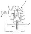
- FIG. 1shows schematically the design of the cylindrical surface discharge electron generating/triggering device of the present invention.
- the cylindrical surface discharge device 10 of the present inventionincludes a cylindrically contoured or cylinder shaped member 12 formed of a dielectric material with dielectric constant ⁇ in excess of 100.
- the cylinder shaped member 12has an external surface 14 and is formed with a central opening 16 extending longitudinally through the cylinder shaped member 12 along the axis of symmetry 18 thereof.
- the central opening 16may be shaped as a cylinder or a cone.
- the surface of the central opening 16defines an internal surface 20 of the cylinder shaped member 12 .
- the diameter of the central opening 16may range from 3 to 15 mm.
- the cylindrical surface discharge device 10further includes an internal electrode 22 having a terminal 24 connected to a power source 26 and an opposite end 28 positioned in contact with the cylinder shaped member 12 in proximity to the edge 30 thereof. Specifically, as shown in FIG. 1 , the internal electrode 22 makes contact at the end 28 to some part of the internal surface 20 of the cylinder shaped member 12 .
- An external electrode 32is connected by the terminal 34 to the power source 26 .
- the external electrode 32is formed as a metallization coating which covers substantially the entire external surface of the cylinder shaped member 12 .
- the cylindrical surface discharge device 10further includes a cylindrical metal electrode (cathode) 36 which has sidewalls 38 and a bottom portion 40 .
- the cathode 36is electrically coupled to the external electrode 32 .
- the bottom portion 40 of the cathode 36is formed with a central bore hole 42 which coincides with the central opening 16 of the cylinder shaped member 12 when the latter is positioned in close proximity to or inside the cathode 36 . In this manner, the sidewalls 38 of the cathode 36 surround the external surface 14 of the cylinder shaped member 12 .
- a dielectric tube 44is attached to the cathode 36 and includes central bore hole 42 . Further, a dielectric insulator plate 46 is positioned between the cathode 36 and an anode 48 to electrically isolate one member from the other. The anode 48 is coupled to a power source 26 , or alternatively to another power source (not shown in the drawing).
- the cylinder shaped member 12 coupled to the power source 26 for receiving a triggering pulse 50represents a trigger portion of the cylindrical surface discharge device of the present invention while the overall design shown in FIG. 1 represents an electron beam generating device.
- the concept underlying the design of the device 10 of the present inventionis the creation of cylindrically shaped discharge which propagates along the surface of high ⁇ dielectric material in order to function as a trigger/generator for axial symmetry devices with an electron concentration such as, for example, electron beam generators.
- a pulsed voltage (triggering pulse) 50When a pulsed voltage (triggering pulse) 50 is applied between the internal electrode 22 and external electrode 32 , a strong electric field in the vicinity of the end 28 of the internal electrode 22 causes electron emission and formation of conducting plasma in the central opening 16 , e.g., triggering the sliding surface discharge.
- the plasma inside the central opening 16expands (slides) along the dielectric internal surface 20 of the cylinder shaped member 12 driven by the longitudinal component of electric field, which exists until the capacitor formed by the dielectric material of the cylinder shaped member 12 and the external electrode 32 is fully charged.
- the dischargeDue to the driving force, the discharge is distributed uniformly over the internal surface 14 .
- the dischargeis terminated only when the surface 14 is totally occupied by plasma.
- the plasmacreates an “electrode” of the cylindrical capacitor formed by the dielectric of the cylinder shaped member 12 having the external electrode 32 on one side thereof and the “plasma electrode” on the internal surface 20 thereof.
- the energy of the dischargecan be controlled by the voltage of the triggering pulse 50 as well as by changing the capacitance of the capacitor formed by the dielectric material and the external electrode 32 in the presence of the plasma electrode.
- the cathode 36As shown in FIG. 1 , the cathode 36 , as well as anode 46 , are coupled to the power source in order that a potential difference exists therebetween which creates an electrical field at least during some portion of the duration of the triggering pulse 50 .
- the electrical field between the cathode 36 and the anode 48facilitates the extraction and acceleration of electrons 52 produced inside the hollow cathode 36 .
- the electrical field dynamically distributed in space between the cathode 36 and the anode 48accelerates the electrons 52 through the dielectric tube 44 , which, in combination with the dielectric insulator plate 46 , constricts the cathode plasma emerging from the hollow cathode bore hole 42 towards the anode 48 .
- the dielectric tube 44 and the insulator dielectric plate 46in addition to constricting the cathode plasma and the electron beam provide for insulation between the cathode 36 and anode 48 so that no discharge occurs between them in absence of the triggering pulse 50 .
- the cylindrically shaped device of the present inventionis a highly effective trigger as well as electron emitter/generator as it provides both the large area plasma and precise location of the elevated concentration of the electrons exactly around the device axis.
- the high ⁇ cylinder shaped member 12focuses the electric field of anode 48 that initially penetrates inside the cathode 36 through the central bore hole 42 . Such a focusing intensifies extraction of the electrons from the plasma inside the central opening 16 of the cylinder shaped member 12 .
- the device of the present inventionprovides sufficient conditions for a pulse discharge device to ignite. When viewed as an electron generator, the device creates electrons and controls the intensity of the discharge.
- the device of the present inventionmay serve as a cathode itself or it can be a part of a cathode assembly, for example, it can be located inside of a hollow cathode and serve as the main trigger unit of an electron source.
Landscapes
- Electron Sources, Ion Sources (AREA)
- Plasma Technology (AREA)
Abstract
Description
The present invention relates to the generation of electrons and in particular to methods of generating spatial regions of high concentrations of electrons.
More in particular, the present invention relates to a technique for generation of initial electrons in pulsed discharge devices with a restricted discharge of cylindrical geometry as for example, in pseudo-spark switches, channel spark discharge devices, etc.
Specifically, the present invention relates to a cylindrical surface discharge device designed to fulfill two functions in combination, such as triggering of the generation of electrons and for generating the electrons, in the form of electron beams. Viewed as a trigger, such a device provides sufficient conditions for a pulse discharge device to ignite. When viewed as a generator, the device creates electron discharge, and to some extent controls the intensity of the discharge.
Further, the present invention relates to a cathode (or cathode assembly) capable of generating a focused electron beam thus functioning as an electron beam source. If the device is located inside of a hollow cathode, then the device may function as a trigger to ignite an electron beam source.
“Free electrons” are the electrons which are controlled, meaning the electrons may be extracted from the electron source, accelerated, and directed in a specified direction. For generation of “free electrons”, the electron source should provide conditions for efficient emission of electrons from a cathode. Direct extraction of electrons from a metal surface by applying an electric field, defined as an auto electron emission requires a high electric field and is known to be limited in the current density.
As an alternative approach to the direct extraction of electrons, electron sources use triggers in which the current pulse passes through a gas, converting it into highly ionized state, called a plasma, which is a good emitter as it has no potential barrier preventing the emission of electrons.
The main electrical triggering technique used in conventional electron generating devices is surface flashover in which a current pulse flows in a gas along a dielectric surface that assists the discharge ignition. For low pressure gases or vacuum, this surface supplies the discharge media (absorbed gas molecules, surface defects, sharp edges, inclusions of foreign materials, etc.). In this technique, discharge literally flashes over the dielectric surface. Disadvantages of such a trigger of the discharge ignition are (1) limited emission of electrons and (2) short lifetime. Both of these disadvantages are related to the fact that current tends to flow through a narrow channel between metallic electrodes of the device. As a result, volume of the plasma channel is limited, and accordingly so is the emitted electron current. Additionally, due to the current confinement into the channel dielectric surface erosion limits lifetime of the trigger to as little as 106pulses.
Other electron emitters make use of some specific material such as dielectrics (or ferro electrics) with high dielectric constant ε˜1000 to overcome the problems associated with limited electron emission and shortened lifetime. A typical electron emitter consists of a dielectric plate mounted between two electrodes positioned on opposite sides thereof, such that one electrode covers the side of the plate completely, while another, e.g., a face electrode, leaves significant area of the side of the dielectric plate uncovered.
Presence of the high ε dielectric facilitates performance of such an electron emitter. First, the emitter can work at lower voltages as it amplifies and focuses an electric field on the edge of the face electrode. Second, it provides distribution of the surface/over-current over larger area as it creates an integrated distributed capacitor that the discharge current tends to charge. Third, due to the distributed nature of the discharge, erosion of the surface is reduced, and lifetime of such a device is elongated.
This design of electron generators/triggers is suitable for large area electron switches or electron guns. However, due to their distributed nature, the design is less effective for some devices where the generated electrons should be concentrated in narrow beams. In this case, only a small fraction of the trigger area, which is located in the vicinity of the device/beam axis, works effectively.
A more effective generator/trigger device than that found in the prior art is needed for generation of focused electron beams.
It is an object of the present invention to provide a surface discharge device for electron beam generation, as well as for discharge triggering to create a sufficient condition for ignition of a pulse discharge for the generation of electrons. Such a device has a controllable intensity of the discharge, long lifetime, and an effective electron emission.
In one aspect, the present invention is a device for electron beam generation which includes a cylindrically contoured member formed of a dielectric material with ε>100; an internal electrode electrically coupled to the cylindrically contoured member on an internal surface defined by a cylindrically or conically shaped central opening extending longitudinally along the symmetry axis of the cylinder-shaped member; an external electrode electrically coupled to the cylinder-shaped member on an external surface thereof; a source of a triggering pulse coupled between the internal and external electrodes; and a cathode member electrically coupled to the external electrode. The sidewalls of the cathode member surround at least a portion of the external surface of the cylindrically contoured member. The bottom of the cathode member has a central bore opening formed therein and disposed in alignment with the central opening of the cylindrically contoured member.
A dielectric tube is secured at one end to the cathode member at the central bore opening, and an anode member is disposed remotely from another end of the dielectric tube. Preferably, an insulation member is positioned between the cathode member and the anode member. The insulation member is attached to the dielectric tube between two ends.
A source of voltage is coupled to the anode member to create a voltage difference between the cathode member and the anode member during at least a portion of a duration of the triggering pulse.
Upon application of the triggering pulse between the internal and external electrodes, an electric field in the vicinity of the internal electrode creates electron emission from the internal surface of the cylinder-shaped member and formation of a conducting plasma in the central opening thereof The conducting plasma expands along the internal surface until a capacitor formed by the cylindrically contoured member and the external electrode is substantially fully charged. The conducting plasma creates a central electrode of the capacitor and triggers the surface discharge along the internal surface of the cylindrically contoured member. The surface discharge stops when the central opening of the cylinder shaped member is substantially completely occupied by the conducting plasma. The electrical field existing between the cathode member and the anode member accelerates electrons of the conducting cathode plasma and extracts these electrons towards the anode member thus forming an electron beam. The dielectric tube constricts the diameter of said plasma.
The energy of the surface discharge is controlled by the amplitude and duration of the triggering pulse and by capacitance of said capacitor.
The present invention further is directed to a method for generating an electron beam, which includes:
- forming a central opening in a cylinder-shaped member formed from a dielectric material having a dielectric constant ε>100,
- connecting an internal electrode to an internal surface of the cylinder-shaped member defined by the central opening,
- connecting an external electrode to an external surface of the cylindrically contoured member,
- positioning the cylinder-shaped member in close proximity to a cathode member, wherein sidewalls of the cathode surround at least a portion of the cylinder-shaped member and the central opening of the cylindrically contoured member is aligned with a central bore opening formed in the bottom of the cathode member;
- coupling the cathode member to the external electrode;
- positioning an anode member remotely from the cathode member;
- applying a triggering pulse between the internal and external electrodes to create electron emission from the internal surface of the cylinder-shaped or cylindrically contoured member and to form conducting plasma in the central opening thereof expanding along the central opening until a capacitor formed by the cylinder-shaped member and the external electrode has been substantially fully charged; and
- applying a voltage to the anode member to create a voltage difference between the cathode and anode members for at lest a portion of a duration of the triggering pulse to accelerate the electrodes of the conducting plasma in the central opening of the cylinder-shaped member and to extract said electrodes from the cathode member through the central bore opening towards the anode member in the form of an electron beam.
Another aspect of the present invention is directed to a trigger in an electron generating device. The trigger includes a cylinder-shaped member formed of a dielectric material. An internal electrode is electrically coupled to the cylinder-shaped member on an internal surface. An external electrode is electrically coupled to the cylinder-shaped member on an external surface. A source of the triggering pulse is coupled between the internal and external electrodes. Upon application of the triggering pulse between the internal and external electrodes, an electric field formed in vicinity of the internal electrode creates electron emission from the internal surface of the cylinder-shaped member and formation of a conducting plasma filling the central opening formed therein. The conducting plasma creates a central electrode of a capacitor formed by the cylinder-shaped member and the external electrode and triggers the surface discharge along the internal surface of the cylinder-shaped member, thereby igniting the electron generating device.
The formation of the conducting plasma is controlled by the amplitude and duration of the triggering pulse and by capacitance of said capacitor.
The present invention further is directed to a method of triggering the generation of electrons in an electron generating device. The triggering method includes the steps of:
- forming a central opening in a cylinder-shaped member made from a dielectric material having a dielectric constant ε>100,
- connecting an internal electrode to an internal surface of the cylinder-shaped member,
- connecting an external electrode to an external surface of the cylinder-shaped member; and
- applying a triggering pulse between said internal and external electrodes to create electrons emission from the internal surface of said cylinder-shaped member and to form conducting plasma in the central opening thereof. The conducting plasma expands along the central opening until a capacitor formed by the cylinder-shaped member and the external electrode has been substantially fully charged thus igniting the electrons generating device.
These features and advantages of the present invention will be fully understood and appreciated from the following Detailed Description of the Accompanying Drawings.
Referring toFIG. 1 , the cylindricalsurface discharge device 10 of the present invention includes a cylindrically contoured or cylinder shapedmember 12 formed of a dielectric material with dielectric constant ε in excess of 100. The cylinder shapedmember 12 has anexternal surface 14 and is formed with acentral opening 16 extending longitudinally through the cylinder shapedmember 12 along the axis ofsymmetry 18 thereof. Thecentral opening 16 may be shaped as a cylinder or a cone. The surface of thecentral opening 16 defines aninternal surface 20 of the cylinder shapedmember 12. The diameter of thecentral opening 16 may range from 3 to 15 mm.
The cylindricalsurface discharge device 10 further includes aninternal electrode 22 having a terminal24 connected to apower source 26 and anopposite end 28 positioned in contact with the cylinder shapedmember 12 in proximity to theedge 30 thereof. Specifically, as shown inFIG. 1 , theinternal electrode 22 makes contact at theend 28 to some part of theinternal surface 20 of the cylinder shapedmember 12.
Anexternal electrode 32 is connected by the terminal34 to thepower source 26. Preferably, theexternal electrode 32 is formed as a metallization coating which covers substantially the entire external surface of the cylinder shapedmember 12.
The cylindricalsurface discharge device 10 further includes a cylindrical metal electrode (cathode)36 which has sidewalls38 and abottom portion 40. Thecathode 36 is electrically coupled to theexternal electrode 32. Thebottom portion 40 of thecathode 36 is formed with acentral bore hole 42 which coincides with thecentral opening 16 of the cylinder shapedmember 12 when the latter is positioned in close proximity to or inside thecathode 36. In this manner, thesidewalls 38 of thecathode 36 surround theexternal surface 14 of the cylinder shapedmember 12.
Adielectric tube 44 is attached to thecathode 36 and includescentral bore hole 42. Further, adielectric insulator plate 46 is positioned between thecathode 36 and ananode 48 to electrically isolate one member from the other. Theanode 48 is coupled to apower source 26, or alternatively to another power source (not shown in the drawing).
In the cylindricalsurface discharge device 10, the cylinder shapedmember 12 coupled to thepower source 26 for receiving a triggeringpulse 50 represents a trigger portion of the cylindrical surface discharge device of the present invention while the overall design shown inFIG. 1 represents an electron beam generating device. The concept underlying the design of thedevice 10 of the present invention is the creation of cylindrically shaped discharge which propagates along the surface of high ε dielectric material in order to function as a trigger/generator for axial symmetry devices with an electron concentration such as, for example, electron beam generators.
When a pulsed voltage (triggering pulse)50 is applied between theinternal electrode 22 andexternal electrode 32, a strong electric field in the vicinity of theend 28 of theinternal electrode 22 causes electron emission and formation of conducting plasma in thecentral opening 16, e.g., triggering the sliding surface discharge. The plasma inside thecentral opening 16 expands (slides) along the dielectricinternal surface 20 of the cylinder shapedmember 12 driven by the longitudinal component of electric field, which exists until the capacitor formed by the dielectric material of the cylinder shapedmember 12 and theexternal electrode 32 is fully charged.
Due to the driving force, the discharge is distributed uniformly over theinternal surface 14. The discharge is terminated only when thesurface 14 is totally occupied by plasma. The plasma creates an “electrode” of the cylindrical capacitor formed by the dielectric of the cylinder shapedmember 12 having theexternal electrode 32 on one side thereof and the “plasma electrode” on theinternal surface 20 thereof. The energy of the discharge can be controlled by the voltage of the triggeringpulse 50 as well as by changing the capacitance of the capacitor formed by the dielectric material and theexternal electrode 32 in the presence of the plasma electrode.
As shown inFIG. 1 , thecathode 36, as well asanode 46, are coupled to the power source in order that a potential difference exists therebetween which creates an electrical field at least during some portion of the duration of the triggeringpulse 50. The electrical field between thecathode 36 and theanode 48 facilitates the extraction and acceleration ofelectrons 52 produced inside thehollow cathode 36. The electrical field dynamically distributed in space between thecathode 36 and theanode 48 accelerates theelectrons 52 through thedielectric tube 44, which, in combination with thedielectric insulator plate 46, constricts the cathode plasma emerging from the hollow cathode borehole 42 towards theanode 48. Thedielectric tube 44 and the insulatordielectric plate 46, in addition to constricting the cathode plasma and the electron beam provide for insulation between thecathode 36 andanode 48 so that no discharge occurs between them in absence of the triggeringpulse 50.
For narrow beam sources of electrons, the cylindrically shaped device of the present invention is a highly effective trigger as well as electron emitter/generator as it provides both the large area plasma and precise location of the elevated concentration of the electrons exactly around the device axis. In addition, the high ε cylinder shapedmember 12 focuses the electric field ofanode 48 that initially penetrates inside thecathode 36 through thecentral bore hole 42. Such a focusing intensifies extraction of the electrons from the plasma inside thecentral opening 16 of the cylinder shapedmember 12. Viewed as a trigger, the device of the present invention provides sufficient conditions for a pulse discharge device to ignite. When viewed as an electron generator, the device creates electrons and controls the intensity of the discharge. The device of the present invention may serve as a cathode itself or it can be a part of a cathode assembly, for example, it can be located inside of a hollow cathode and serve as the main trigger unit of an electron source.
Although this invention has been described in connection with specific forms and embodiments thereof, it will be appreciated that various modifications other than those discussed above may be resorted to without departing from the spirit or scope of the invention as defined in the appended Claims. For example, equivalent elements may be substituted for those specifically shown and described, certain features may be used independently of other features, and in certain cases, particular locations of elements may be reversed or interposed, all without departing from the spirit or scope of the invention as defined in the appended Claims.
Claims (29)
1. Electron beam generating device, comprising:
a cylinder-shaped member formed of a dielectric material having a dielectric constant ε>100, said cylinder-shaped member having an external surface and a central opening formed therethrough defining an internal surface thereof, said central opening extending longitudinally along the symmetrical axis of said cylinder-shaped member;
an internal electrode electrically coupled to said cylinder-shaped member at said internal surface thereof;
an external electrode electrically coupled to said cylinder-shaped member at said external surface thereof;
triggering source means for triggering a pulse, said triggering source means coupled between said internal and external electrodes;
a cathode member electrically coupled to said external electrode, said cathode member having sidewalls and a bottom section, the sidewalls of said cathode member being in surrounding relationship with at least a portion of said external surface of said cylinder-shaped member, said bottom section of said cathode member having a central bore opening formed therein and disposed in alignment with said central opening of said cylinder-shaped member; and
an anode member disposed remotely from said central bore opening along said symmetrical axis of said cylinder-shaped member, wherein, upon application of said pulse between said internal and external electrodes, a sliding surface discharge is created along said internal surface of said cylinder-shaped member to produce electrons, said electrons being concentrated at said symmetrical axis of said cylinder-shaped member, and wherein an electrical field between said cathode and anode members accelerates said concentrated electrons to a high energy, thus forming a high-energy electron beam, and extracts said high energy electron beam through said central bore opening of said cathode member towards said anode member.
2. The device ofclaim 1 , further comprising means for creating a voltage difference between said cathode member and said anode member during at least a portion of duration of said triggering pulse, said means for creating said voltage difference being coupled to said anode member.
3. The device ofclaim 1 , further comprising an insulation member disposed between said cathode member and said anode member.
4. The device ofclaim 1 , further comprising a dielectric tube secured by one end thereof to said cathode member at said central bore opening thereof, said anode member being disposed remotely from another end of said dielectric tube.
5. The device ofclaim 1 , wherein said internal electrode is disposed in said central opening of said cylinder-shaped member.
6. The device ofclaim 1 , wherein said internal electrode is disposed in contact with a portion of said internal surface of said cylinder-shaped member.
7. The device ofclaim 1 , wherein said central opening of said cylinder-shaped member is cylindrically shaped.
8. The device ofclaim 1 , wherein said central opening of said cylinder-shaped member is conically-shaped.
9. The device ofclaim 1 , wherein the diameter of said central opening of said cylinder-shaped member is in the range of 3–15 mm.
10. The device ofclaim 1 , wherein said external electrode envelopes said external surface of said cylinder-shaped member.
11. The device ofclaim 10 , wherein said external surface of said cylinder-shaped member is metallized, said metallization forming said external electrode.
12. The device ofclaim 4 , wherein said dielectric tube constricts a diameter of a cathode plasma and an electron beam formed of electrons migrating from said cathode member to said anode member.
13. A method for generating an electron beam, comprising the steps of:
forming a central opening in a cylinder-shaped member formed from a dielectric material having a dielectric constant ε>100, said central opening extending longitudinally of said cylinder-shaped member along the axis of symmetry thereof;
connecting an internal electrode to an internal surface of said cylinder-shaped member, said internal surface being defined by said central opening;
connecting an external electrode to an external surface of said cylinder-shaped member;
positioning said cylinder-shaped member in proximity to a cathode member having sidewalls and a bottom, said sidewalls of said cathode member being in surrounding relationship with at least a portion of said external surface of said cylinder-shaped member, said central opening of said cylinder-shaped member being substantially aligned with a central bore opening formed in said bottom of said cathode member;
electrically coupling said cathode member to said external electrode;
positioning an anode member remotely from said cathode member;
applying a triggering pulse between said internal and external electrodes to create electrons emission from said internal surface of said cylinder-shaped member and to form conducting plasma in said central opening thereof expanding along said central opening until a capacitor formed by said cylinder-shaped member and said external electrode has been substantially fully charged; and
applying a voltage to said anode member to create a voltage difference between said cathode and anode members for at least a portion of a duration of said triggering pulse to accelerate the electrons of said conducting plasma in said central opening of said cylinder-shaped member and to extract said electrons from said plasma through said central bore opening towards said anode member in the form of a electron beam.
14. The method ofclaim 13 , further comprising the step of:
attaching one end of a dielectric tube to said central bore opening formed in said cathode member to constrict the diameter of said plasma and electron beam.
15. The method ofclaim 14 , further comprising the step of:
attaching an insulating member to said dielectric tube between said cathode member and said anode member.
16. The method ofclaim 13 , further comprising the step of:
forming said central opening in said cylinder-shaped member in the contour of a cylinder.
17. The method ofclaim 13 , further comprising the step of:
forming said central opening in said cylinder-shaped member in a form of a cone.
18. The method ofclaim 13 , further comprising the step of:
metallizing said external surface of said cylinder-shaped member to form said external electrode.
19. The method ofclaim 13 , further comprising the step of:
triggering the surface discharge on said internal surface of said cylinder-shaped member.
20. The method ofclaim 19 , further comprising the step of:
controlling the energy of the surface discharge by varying an amplitude and duration of said triggering pulse.
21. The method ofclaim 19 , further comprising the step of:
controlling the energy of the surface discharge by varying the capacitance of said capacitor.
22. A trigger in an electron generating device, the trigger comprising:
a cylinder-shaped member made of a dielectric material, said cylinder-shaped member having an external surface and a central opening formed in said cylinder-shaped member, said central opening extending longitudinally along the symmetry axis of said cylinder-shaped members and defining an internal surface thereof;
an internal electrode electrically coupled to said cylinder-shaped member at said internal surface thereof;
an external electrode electrically coupled to said cylinder-shaped member at said external surface thereof; and
a source of a triggering pulse coupled between said internal and external electrodes,
wherein, upon application of said triggering pulse between said internal and external electrodes, an electric field in vicinity of said internal electrode creates electrons emission from said internal surface of said cylinder-shaped member and formation of conducting plasma filling said central opening thereof, thus igniting the electron generating device to produce a beam of high-energy electrons, wherein said conducting plasma expands along said internal surface until a capacitor formed by said cylinder-shaped member and said external electrode is substantially fully charged.
23. The trigger ofclaim 22 , wherein said external surface of said cylinder-shaped member is metallized, said metallization forming said external electrode.
24. The trigger ofclaim 22 , wherein said central opening is a cylindrically shaped opening.
25. The trigger ofclaim 22 , wherein said central opening is a conically shaped opening.
26. A method of triggering generation of electrons in an electrons generating device, comprising the steps of:
forming a central opening in a cylinder-shaped member made from a dielectric material having a dielectric constant ε>100, said central opening extending longitudinally said cylinder-shaped member along the axis of symmetry thereof;
connecting an internal electrode to an internal surface of said cylinder-shaped member, said internal surface being defined by said central opening;
connecting an external electrode to an external surface of said cylinder-shaped member; and
applying a triggering pulse between said internal and external electrodes to create emission of electrons from said internal surface of said cylinder-shaped member and to form conducting plasma in said central opening thereof, thus igniting the electrons generating device, wherein said emitted electrons are concentrated at said axis of symmetry of said cylinder-shaped member, and wherein an electrical field applied to said conducting plasma accelerates said concentrated electrons to a high energy, thus producing a high-energy electron beam.
27. The method ofclaim 26 , further comprising the steps of:
metallizing said external surface of said cylinder-shaped member to form said external contact.
28. The method ofclaim 26 , further comprising the step of:
controlling the formation of said conducting plasma by changing an amplitude and duration of the triggering pulse.
29. The method ofclaim 26 , further comprising the step of controlling the formation of said conducting plasma by changing the capacitance of said capacitor.
Priority Applications (1)
| Application Number | Priority Date | Filing Date | Title |
|---|---|---|---|
| US10/870,992US7122949B2 (en) | 2004-06-21 | 2004-06-21 | Cylindrical electron beam generating/triggering device and method for generation of electrons |
Applications Claiming Priority (1)
| Application Number | Priority Date | Filing Date | Title |
|---|---|---|---|
| US10/870,992US7122949B2 (en) | 2004-06-21 | 2004-06-21 | Cylindrical electron beam generating/triggering device and method for generation of electrons |
Publications (2)
| Publication Number | Publication Date |
|---|---|
| US20050280345A1 US20050280345A1 (en) | 2005-12-22 |
| US7122949B2true US7122949B2 (en) | 2006-10-17 |
Family
ID=35479912
Family Applications (1)
| Application Number | Title | Priority Date | Filing Date |
|---|---|---|---|
| US10/870,992Expired - LifetimeUS7122949B2 (en) | 2004-06-21 | 2004-06-21 | Cylindrical electron beam generating/triggering device and method for generation of electrons |
Country Status (1)
| Country | Link |
|---|---|
| US (1) | US7122949B2 (en) |
Cited By (158)
| Publication number | Priority date | Publication date | Assignee | Title |
|---|---|---|---|---|
| US20050012441A1 (en)* | 2002-02-25 | 2005-01-20 | Christoph Schulteiss | Channel spark source for generating a stable focussed electron beam |
| US20050218507A1 (en)* | 2004-02-26 | 2005-10-06 | Applied Materials, Inc. | Lid assembly for front end of line fabrication |
| RU2387039C1 (en)* | 2008-12-15 | 2010-04-20 | Российская Федерация, от имени которой выступает государственный заказчик - Государственная корпорация по атомной энергии "Росатом" | High-frequency generator with discharge in hollow cathode |
| US7780793B2 (en) | 2004-02-26 | 2010-08-24 | Applied Materials, Inc. | Passivation layer formation by plasma clean process to reduce native oxide growth |
| RU2497225C2 (en)* | 2012-01-10 | 2013-10-27 | Российская Федерация, от имени которой выступает Государственная корпорация по атомной энергии "Росатом" - Госкорпорация "Росатом" | Generator of high-frequency emission based on discharge with hollow cathode |
| US8679982B2 (en) | 2011-08-26 | 2014-03-25 | Applied Materials, Inc. | Selective suppression of dry-etch rate of materials containing both silicon and oxygen |
| US8679983B2 (en) | 2011-09-01 | 2014-03-25 | Applied Materials, Inc. | Selective suppression of dry-etch rate of materials containing both silicon and nitrogen |
| US8765574B2 (en) | 2012-11-09 | 2014-07-01 | Applied Materials, Inc. | Dry etch process |
| US8771539B2 (en) | 2011-02-22 | 2014-07-08 | Applied Materials, Inc. | Remotely-excited fluorine and water vapor etch |
| US8801952B1 (en) | 2013-03-07 | 2014-08-12 | Applied Materials, Inc. | Conformal oxide dry etch |
| US8808563B2 (en) | 2011-10-07 | 2014-08-19 | Applied Materials, Inc. | Selective etch of silicon by way of metastable hydrogen termination |
| US8895449B1 (en) | 2013-05-16 | 2014-11-25 | Applied Materials, Inc. | Delicate dry clean |
| US8921234B2 (en) | 2012-12-21 | 2014-12-30 | Applied Materials, Inc. | Selective titanium nitride etching |
| US8927390B2 (en) | 2011-09-26 | 2015-01-06 | Applied Materials, Inc. | Intrench profile |
| US8951429B1 (en) | 2013-10-29 | 2015-02-10 | Applied Materials, Inc. | Tungsten oxide processing |
| US8956980B1 (en) | 2013-09-16 | 2015-02-17 | Applied Materials, Inc. | Selective etch of silicon nitride |
| US8969212B2 (en) | 2012-11-20 | 2015-03-03 | Applied Materials, Inc. | Dry-etch selectivity |
| US8975152B2 (en) | 2011-11-08 | 2015-03-10 | Applied Materials, Inc. | Methods of reducing substrate dislocation during gapfill processing |
| US8980763B2 (en) | 2012-11-30 | 2015-03-17 | Applied Materials, Inc. | Dry-etch for selective tungsten removal |
| US8999856B2 (en) | 2011-03-14 | 2015-04-07 | Applied Materials, Inc. | Methods for etch of sin films |
| US9023732B2 (en) | 2013-03-15 | 2015-05-05 | Applied Materials, Inc. | Processing systems and methods for halide scavenging |
| US9023734B2 (en) | 2012-09-18 | 2015-05-05 | Applied Materials, Inc. | Radical-component oxide etch |
| US9034770B2 (en) | 2012-09-17 | 2015-05-19 | Applied Materials, Inc. | Differential silicon oxide etch |
| US9040422B2 (en) | 2013-03-05 | 2015-05-26 | Applied Materials, Inc. | Selective titanium nitride removal |
| US9064816B2 (en) | 2012-11-30 | 2015-06-23 | Applied Materials, Inc. | Dry-etch for selective oxidation removal |
| US9064815B2 (en) | 2011-03-14 | 2015-06-23 | Applied Materials, Inc. | Methods for etch of metal and metal-oxide films |
| US9111877B2 (en) | 2012-12-18 | 2015-08-18 | Applied Materials, Inc. | Non-local plasma oxide etch |
| US9114438B2 (en) | 2013-05-21 | 2015-08-25 | Applied Materials, Inc. | Copper residue chamber clean |
| US9117855B2 (en) | 2013-12-04 | 2015-08-25 | Applied Materials, Inc. | Polarity control for remote plasma |
| US9132436B2 (en) | 2012-09-21 | 2015-09-15 | Applied Materials, Inc. | Chemical control features in wafer process equipment |
| US9136273B1 (en) | 2014-03-21 | 2015-09-15 | Applied Materials, Inc. | Flash gate air gap |
| US9159606B1 (en) | 2014-07-31 | 2015-10-13 | Applied Materials, Inc. | Metal air gap |
| US9165786B1 (en) | 2014-08-05 | 2015-10-20 | Applied Materials, Inc. | Integrated oxide and nitride recess for better channel contact in 3D architectures |
| US9190293B2 (en) | 2013-12-18 | 2015-11-17 | Applied Materials, Inc. | Even tungsten etch for high aspect ratio trenches |
| US9236265B2 (en) | 2013-11-04 | 2016-01-12 | Applied Materials, Inc. | Silicon germanium processing |
| US9236266B2 (en) | 2011-08-01 | 2016-01-12 | Applied Materials, Inc. | Dry-etch for silicon-and-carbon-containing films |
| US9245762B2 (en) | 2013-12-02 | 2016-01-26 | Applied Materials, Inc. | Procedure for etch rate consistency |
| US9263278B2 (en) | 2013-12-17 | 2016-02-16 | Applied Materials, Inc. | Dopant etch selectivity control |
| US9269590B2 (en) | 2014-04-07 | 2016-02-23 | Applied Materials, Inc. | Spacer formation |
| US9287134B2 (en) | 2014-01-17 | 2016-03-15 | Applied Materials, Inc. | Titanium oxide etch |
| US9287095B2 (en) | 2013-12-17 | 2016-03-15 | Applied Materials, Inc. | Semiconductor system assemblies and methods of operation |
| US9293568B2 (en) | 2014-01-27 | 2016-03-22 | Applied Materials, Inc. | Method of fin patterning |
| US9299575B2 (en) | 2014-03-17 | 2016-03-29 | Applied Materials, Inc. | Gas-phase tungsten etch |
| US9299537B2 (en) | 2014-03-20 | 2016-03-29 | Applied Materials, Inc. | Radial waveguide systems and methods for post-match control of microwaves |
| US9299582B2 (en) | 2013-11-12 | 2016-03-29 | Applied Materials, Inc. | Selective etch for metal-containing materials |
| US9299538B2 (en) | 2014-03-20 | 2016-03-29 | Applied Materials, Inc. | Radial waveguide systems and methods for post-match control of microwaves |
| US9299583B1 (en) | 2014-12-05 | 2016-03-29 | Applied Materials, Inc. | Aluminum oxide selective etch |
| US9309598B2 (en) | 2014-05-28 | 2016-04-12 | Applied Materials, Inc. | Oxide and metal removal |
| US9324576B2 (en) | 2010-05-27 | 2016-04-26 | Applied Materials, Inc. | Selective etch for silicon films |
| US9343272B1 (en) | 2015-01-08 | 2016-05-17 | Applied Materials, Inc. | Self-aligned process |
| US9349605B1 (en) | 2015-08-07 | 2016-05-24 | Applied Materials, Inc. | Oxide etch selectivity systems and methods |
| US9355856B2 (en) | 2014-09-12 | 2016-05-31 | Applied Materials, Inc. | V trench dry etch |
| US9355862B2 (en) | 2014-09-24 | 2016-05-31 | Applied Materials, Inc. | Fluorine-based hardmask removal |
| US9362130B2 (en) | 2013-03-01 | 2016-06-07 | Applied Materials, Inc. | Enhanced etching processes using remote plasma sources |
| US9368364B2 (en) | 2014-09-24 | 2016-06-14 | Applied Materials, Inc. | Silicon etch process with tunable selectivity to SiO2 and other materials |
| US9373517B2 (en) | 2012-08-02 | 2016-06-21 | Applied Materials, Inc. | Semiconductor processing with DC assisted RF power for improved control |
| US9373522B1 (en) | 2015-01-22 | 2016-06-21 | Applied Mateials, Inc. | Titanium nitride removal |
| US9378978B2 (en) | 2014-07-31 | 2016-06-28 | Applied Materials, Inc. | Integrated oxide recess and floating gate fin trimming |
| US9378969B2 (en) | 2014-06-19 | 2016-06-28 | Applied Materials, Inc. | Low temperature gas-phase carbon removal |
| US9385028B2 (en) | 2014-02-03 | 2016-07-05 | Applied Materials, Inc. | Air gap process |
| US9390937B2 (en) | 2012-09-20 | 2016-07-12 | Applied Materials, Inc. | Silicon-carbon-nitride selective etch |
| US9396989B2 (en) | 2014-01-27 | 2016-07-19 | Applied Materials, Inc. | Air gaps between copper lines |
| US9406523B2 (en) | 2014-06-19 | 2016-08-02 | Applied Materials, Inc. | Highly selective doped oxide removal method |
| US9425058B2 (en) | 2014-07-24 | 2016-08-23 | Applied Materials, Inc. | Simplified litho-etch-litho-etch process |
| US9449846B2 (en) | 2015-01-28 | 2016-09-20 | Applied Materials, Inc. | Vertical gate separation |
| US9478432B2 (en) | 2014-09-25 | 2016-10-25 | Applied Materials, Inc. | Silicon oxide selective removal |
| US9496167B2 (en) | 2014-07-31 | 2016-11-15 | Applied Materials, Inc. | Integrated bit-line airgap formation and gate stack post clean |
| US9493879B2 (en) | 2013-07-12 | 2016-11-15 | Applied Materials, Inc. | Selective sputtering for pattern transfer |
| US9502258B2 (en) | 2014-12-23 | 2016-11-22 | Applied Materials, Inc. | Anisotropic gap etch |
| US9499898B2 (en) | 2014-03-03 | 2016-11-22 | Applied Materials, Inc. | Layered thin film heater and method of fabrication |
| US9553102B2 (en) | 2014-08-19 | 2017-01-24 | Applied Materials, Inc. | Tungsten separation |
| US9576809B2 (en) | 2013-11-04 | 2017-02-21 | Applied Materials, Inc. | Etch suppression with germanium |
| US9659753B2 (en) | 2014-08-07 | 2017-05-23 | Applied Materials, Inc. | Grooved insulator to reduce leakage current |
| US9691645B2 (en) | 2015-08-06 | 2017-06-27 | Applied Materials, Inc. | Bolted wafer chuck thermal management systems and methods for wafer processing systems |
| US9721789B1 (en) | 2016-10-04 | 2017-08-01 | Applied Materials, Inc. | Saving ion-damaged spacers |
| US9728437B2 (en) | 2015-02-03 | 2017-08-08 | Applied Materials, Inc. | High temperature chuck for plasma processing systems |
| US9741593B2 (en) | 2015-08-06 | 2017-08-22 | Applied Materials, Inc. | Thermal management systems and methods for wafer processing systems |
| US9768034B1 (en) | 2016-11-11 | 2017-09-19 | Applied Materials, Inc. | Removal methods for high aspect ratio structures |
| US9773648B2 (en) | 2013-08-30 | 2017-09-26 | Applied Materials, Inc. | Dual discharge modes operation for remote plasma |
| US9847289B2 (en) | 2014-05-30 | 2017-12-19 | Applied Materials, Inc. | Protective via cap for improved interconnect performance |
| US9865484B1 (en) | 2016-06-29 | 2018-01-09 | Applied Materials, Inc. | Selective etch using material modification and RF pulsing |
| US9881805B2 (en) | 2015-03-02 | 2018-01-30 | Applied Materials, Inc. | Silicon selective removal |
| US9885117B2 (en) | 2014-03-31 | 2018-02-06 | Applied Materials, Inc. | Conditioned semiconductor system parts |
| US9934942B1 (en) | 2016-10-04 | 2018-04-03 | Applied Materials, Inc. | Chamber with flow-through source |
| US9947549B1 (en) | 2016-10-10 | 2018-04-17 | Applied Materials, Inc. | Cobalt-containing material removal |
| RU2657240C1 (en)* | 2017-01-24 | 2018-06-09 | Российская Федерация, от имени которой выступает Государственная корпорация по атомной энергии "Росатом" (Госкорпорация "Росатом") | Generator of high frequency pulses on the basis of discharge with full cathode |
| US10026621B2 (en) | 2016-11-14 | 2018-07-17 | Applied Materials, Inc. | SiN spacer profile patterning |
| US10043674B1 (en) | 2017-08-04 | 2018-08-07 | Applied Materials, Inc. | Germanium etching systems and methods |
| US10043684B1 (en) | 2017-02-06 | 2018-08-07 | Applied Materials, Inc. | Self-limiting atomic thermal etching systems and methods |
| US10049891B1 (en) | 2017-05-31 | 2018-08-14 | Applied Materials, Inc. | Selective in situ cobalt residue removal |
| US10062579B2 (en) | 2016-10-07 | 2018-08-28 | Applied Materials, Inc. | Selective SiN lateral recess |
| US10062575B2 (en) | 2016-09-09 | 2018-08-28 | Applied Materials, Inc. | Poly directional etch by oxidation |
| US10062587B2 (en) | 2012-07-18 | 2018-08-28 | Applied Materials, Inc. | Pedestal with multi-zone temperature control and multiple purge capabilities |
| US10062585B2 (en) | 2016-10-04 | 2018-08-28 | Applied Materials, Inc. | Oxygen compatible plasma source |
| US10128086B1 (en) | 2017-10-24 | 2018-11-13 | Applied Materials, Inc. | Silicon pretreatment for nitride removal |
| US10163696B2 (en) | 2016-11-11 | 2018-12-25 | Applied Materials, Inc. | Selective cobalt removal for bottom up gapfill |
| US10170282B2 (en) | 2013-03-08 | 2019-01-01 | Applied Materials, Inc. | Insulated semiconductor faceplate designs |
| US10170336B1 (en) | 2017-08-04 | 2019-01-01 | Applied Materials, Inc. | Methods for anisotropic control of selective silicon removal |
| US10224210B2 (en) | 2014-12-09 | 2019-03-05 | Applied Materials, Inc. | Plasma processing system with direct outlet toroidal plasma source |
| US10242908B2 (en) | 2016-11-14 | 2019-03-26 | Applied Materials, Inc. | Airgap formation with damage-free copper |
| US10256112B1 (en) | 2017-12-08 | 2019-04-09 | Applied Materials, Inc. | Selective tungsten removal |
| US10256079B2 (en) | 2013-02-08 | 2019-04-09 | Applied Materials, Inc. | Semiconductor processing systems having multiple plasma configurations |
| US10283321B2 (en) | 2011-01-18 | 2019-05-07 | Applied Materials, Inc. | Semiconductor processing system and methods using capacitively coupled plasma |
| US10283324B1 (en) | 2017-10-24 | 2019-05-07 | Applied Materials, Inc. | Oxygen treatment for nitride etching |
| US10297458B2 (en) | 2017-08-07 | 2019-05-21 | Applied Materials, Inc. | Process window widening using coated parts in plasma etch processes |
| US10319600B1 (en) | 2018-03-12 | 2019-06-11 | Applied Materials, Inc. | Thermal silicon etch |
| US10319649B2 (en) | 2017-04-11 | 2019-06-11 | Applied Materials, Inc. | Optical emission spectroscopy (OES) for remote plasma monitoring |
| US10319739B2 (en) | 2017-02-08 | 2019-06-11 | Applied Materials, Inc. | Accommodating imperfectly aligned memory holes |
| US10354889B2 (en) | 2017-07-17 | 2019-07-16 | Applied Materials, Inc. | Non-halogen etching of silicon-containing materials |
| US10403507B2 (en) | 2017-02-03 | 2019-09-03 | Applied Materials, Inc. | Shaped etch profile with oxidation |
| US10431429B2 (en) | 2017-02-03 | 2019-10-01 | Applied Materials, Inc. | Systems and methods for radial and azimuthal control of plasma uniformity |
| US10468267B2 (en) | 2017-05-31 | 2019-11-05 | Applied Materials, Inc. | Water-free etching methods |
| US10490406B2 (en) | 2018-04-10 | 2019-11-26 | Appled Materials, Inc. | Systems and methods for material breakthrough |
| US10490418B2 (en) | 2014-10-14 | 2019-11-26 | Applied Materials, Inc. | Systems and methods for internal surface conditioning assessment in plasma processing equipment |
| US10497573B2 (en) | 2018-03-13 | 2019-12-03 | Applied Materials, Inc. | Selective atomic layer etching of semiconductor materials |
| US10504700B2 (en) | 2015-08-27 | 2019-12-10 | Applied Materials, Inc. | Plasma etching systems and methods with secondary plasma injection |
| US10504754B2 (en) | 2016-05-19 | 2019-12-10 | Applied Materials, Inc. | Systems and methods for improved semiconductor etching and component protection |
| US10522371B2 (en) | 2016-05-19 | 2019-12-31 | Applied Materials, Inc. | Systems and methods for improved semiconductor etching and component protection |
| US10541184B2 (en) | 2017-07-11 | 2020-01-21 | Applied Materials, Inc. | Optical emission spectroscopic techniques for monitoring etching |
| US10541246B2 (en) | 2017-06-26 | 2020-01-21 | Applied Materials, Inc. | 3D flash memory cells which discourage cross-cell electrical tunneling |
| US10546729B2 (en) | 2016-10-04 | 2020-01-28 | Applied Materials, Inc. | Dual-channel showerhead with improved profile |
| US10566206B2 (en) | 2016-12-27 | 2020-02-18 | Applied Materials, Inc. | Systems and methods for anisotropic material breakthrough |
| US10573527B2 (en) | 2018-04-06 | 2020-02-25 | Applied Materials, Inc. | Gas-phase selective etching systems and methods |
| US10573496B2 (en) | 2014-12-09 | 2020-02-25 | Applied Materials, Inc. | Direct outlet toroidal plasma source |
| US10593560B2 (en) | 2018-03-01 | 2020-03-17 | Applied Materials, Inc. | Magnetic induction plasma source for semiconductor processes and equipment |
| US10593523B2 (en) | 2014-10-14 | 2020-03-17 | Applied Materials, Inc. | Systems and methods for internal surface conditioning in plasma processing equipment |
| RU2717091C1 (en)* | 2019-09-20 | 2020-03-18 | Российская Федерация, от имени которой выступает Государственная корпорация по атомной энергии "Росатом" (Госкорпорация "Росатом") | High-frequency pulse gas-discharge generator |
| US10615047B2 (en) | 2018-02-28 | 2020-04-07 | Applied Materials, Inc. | Systems and methods to form airgaps |
| US10629473B2 (en) | 2016-09-09 | 2020-04-21 | Applied Materials, Inc. | Footing removal for nitride spacer |
| RU2722228C1 (en)* | 2019-05-17 | 2020-05-28 | Российская Федерация, от имени которой выступает Государственная корпорация по атомной энергии "Росатом" (Госкорпорация "Росатом") | High-frequency pulses generator based on hollow cathode discharge |
| US10672642B2 (en) | 2018-07-24 | 2020-06-02 | Applied Materials, Inc. | Systems and methods for pedestal configuration |
| US10679870B2 (en) | 2018-02-15 | 2020-06-09 | Applied Materials, Inc. | Semiconductor processing chamber multistage mixing apparatus |
| US10699879B2 (en) | 2018-04-17 | 2020-06-30 | Applied Materials, Inc. | Two piece electrode assembly with gap for plasma control |
| US10727080B2 (en) | 2017-07-07 | 2020-07-28 | Applied Materials, Inc. | Tantalum-containing material removal |
| US10755941B2 (en) | 2018-07-06 | 2020-08-25 | Applied Materials, Inc. | Self-limiting selective etching systems and methods |
| US10854426B2 (en) | 2018-01-08 | 2020-12-01 | Applied Materials, Inc. | Metal recess for semiconductor structures |
| US10872778B2 (en) | 2018-07-06 | 2020-12-22 | Applied Materials, Inc. | Systems and methods utilizing solid-phase etchants |
| US10886137B2 (en) | 2018-04-30 | 2021-01-05 | Applied Materials, Inc. | Selective nitride removal |
| US10892198B2 (en) | 2018-09-14 | 2021-01-12 | Applied Materials, Inc. | Systems and methods for improved performance in semiconductor processing |
| US10903054B2 (en) | 2017-12-19 | 2021-01-26 | Applied Materials, Inc. | Multi-zone gas distribution systems and methods |
| US10920319B2 (en) | 2019-01-11 | 2021-02-16 | Applied Materials, Inc. | Ceramic showerheads with conductive electrodes |
| US10920320B2 (en) | 2017-06-16 | 2021-02-16 | Applied Materials, Inc. | Plasma health determination in semiconductor substrate processing reactors |
| US10943834B2 (en) | 2017-03-13 | 2021-03-09 | Applied Materials, Inc. | Replacement contact process |
| US10964512B2 (en) | 2018-02-15 | 2021-03-30 | Applied Materials, Inc. | Semiconductor processing chamber multistage mixing apparatus and methods |
| US11049755B2 (en) | 2018-09-14 | 2021-06-29 | Applied Materials, Inc. | Semiconductor substrate supports with embedded RF shield |
| US11062887B2 (en) | 2018-09-17 | 2021-07-13 | Applied Materials, Inc. | High temperature RF heater pedestals |
| US11121002B2 (en) | 2018-10-24 | 2021-09-14 | Applied Materials, Inc. | Systems and methods for etching metals and metal derivatives |
| US11239061B2 (en) | 2014-11-26 | 2022-02-01 | Applied Materials, Inc. | Methods and systems to enhance process uniformity |
| US11257693B2 (en) | 2015-01-09 | 2022-02-22 | Applied Materials, Inc. | Methods and systems to improve pedestal temperature control |
| US11276559B2 (en) | 2017-05-17 | 2022-03-15 | Applied Materials, Inc. | Semiconductor processing chamber for multiple precursor flow |
| US11276590B2 (en) | 2017-05-17 | 2022-03-15 | Applied Materials, Inc. | Multi-zone semiconductor substrate supports |
| US11328909B2 (en) | 2017-12-22 | 2022-05-10 | Applied Materials, Inc. | Chamber conditioning and removal processes |
| US11417534B2 (en) | 2018-09-21 | 2022-08-16 | Applied Materials, Inc. | Selective material removal |
| US11437242B2 (en) | 2018-11-27 | 2022-09-06 | Applied Materials, Inc. | Selective removal of silicon-containing materials |
| US11594428B2 (en) | 2015-02-03 | 2023-02-28 | Applied Materials, Inc. | Low temperature chuck for plasma processing systems |
| US11682560B2 (en) | 2018-10-11 | 2023-06-20 | Applied Materials, Inc. | Systems and methods for hafnium-containing film removal |
| US11721527B2 (en) | 2019-01-07 | 2023-08-08 | Applied Materials, Inc. | Processing chamber mixing systems |
| US12340979B2 (en) | 2017-05-17 | 2025-06-24 | Applied Materials, Inc. | Semiconductor processing chamber for improved precursor flow |
Families Citing this family (3)
| Publication number | Priority date | Publication date | Assignee | Title |
|---|---|---|---|---|
| RU2651580C1 (en)* | 2017-01-11 | 2018-04-23 | Российская Федерация, от имени которой выступает Государственная корпорация по атомной энергии "Росатом" (Госкорпорация "Росатом") | Generator of high frequency pulses on the basis of discharge with full cathode |
| RU2751542C1 (en)* | 2020-11-06 | 2021-07-14 | Российская Федерация, от имени которой выступает Государственная корпорация по атомной энергии "Росатом" (Госкорпорация "Росатом") | Gas-discharge generator of high-frequency pulses |
| RU209937U1 (en)* | 2021-04-12 | 2022-03-24 | Российская Федерация, от имени которой выступает Государственная корпорация по атомной энергии "Росатом" (Госкорпорация "Росатом") | PORTABLE GAS-DISCHARGE HIGH-FREQUENCY PULSE GENERATOR |
Citations (6)
| Publication number | Priority date | Publication date | Assignee | Title |
|---|---|---|---|---|
| US5276386A (en)* | 1991-03-06 | 1994-01-04 | Hitachi, Ltd. | Microwave plasma generating method and apparatus |
| US5389902A (en)* | 1992-11-09 | 1995-02-14 | Elmec Corporation | Electromagnetic delay line having a plurality of chip capacitors disposed in more than one row |
| US6422172B1 (en)* | 1997-03-19 | 2002-07-23 | Hitachi, Ltd. | Plasma processing apparatus and plasma processing method |
| US6441554B1 (en)* | 2000-11-28 | 2002-08-27 | Se Plasma Inc. | Apparatus for generating low temperature plasma at atmospheric pressure |
| US6617770B2 (en)* | 2001-03-09 | 2003-09-09 | Shinko Electric Industries Co., Ltd | Gas filled switching electric discharge tube |
| US6800336B1 (en)* | 1999-10-30 | 2004-10-05 | Foernsel Peter | Method and device for plasma coating surfaces |
- 2004
- 2004-06-21USUS10/870,992patent/US7122949B2/ennot_activeExpired - Lifetime
Patent Citations (6)
| Publication number | Priority date | Publication date | Assignee | Title |
|---|---|---|---|---|
| US5276386A (en)* | 1991-03-06 | 1994-01-04 | Hitachi, Ltd. | Microwave plasma generating method and apparatus |
| US5389902A (en)* | 1992-11-09 | 1995-02-14 | Elmec Corporation | Electromagnetic delay line having a plurality of chip capacitors disposed in more than one row |
| US6422172B1 (en)* | 1997-03-19 | 2002-07-23 | Hitachi, Ltd. | Plasma processing apparatus and plasma processing method |
| US6800336B1 (en)* | 1999-10-30 | 2004-10-05 | Foernsel Peter | Method and device for plasma coating surfaces |
| US6441554B1 (en)* | 2000-11-28 | 2002-08-27 | Se Plasma Inc. | Apparatus for generating low temperature plasma at atmospheric pressure |
| US6617770B2 (en)* | 2001-03-09 | 2003-09-09 | Shinko Electric Industries Co., Ltd | Gas filled switching electric discharge tube |
Cited By (235)
| Publication number | Priority date | Publication date | Assignee | Title |
|---|---|---|---|---|
| US7183564B2 (en)* | 2002-02-25 | 2007-02-27 | Forschungszentrum Karlsruhe Gmbh | Channel spark source for generating a stable focused electron beam |
| US20050012441A1 (en)* | 2002-02-25 | 2005-01-20 | Christoph Schulteiss | Channel spark source for generating a stable focussed electron beam |
| US7520957B2 (en)* | 2004-02-26 | 2009-04-21 | Applied Materials, Inc. | Lid assembly for front end of line fabrication |
| US7767024B2 (en) | 2004-02-26 | 2010-08-03 | Appplied Materials, Inc. | Method for front end of line fabrication |
| US7780793B2 (en) | 2004-02-26 | 2010-08-24 | Applied Materials, Inc. | Passivation layer formation by plasma clean process to reduce native oxide growth |
| US8343307B2 (en) | 2004-02-26 | 2013-01-01 | Applied Materials, Inc. | Showerhead assembly |
| US20050218507A1 (en)* | 2004-02-26 | 2005-10-06 | Applied Materials, Inc. | Lid assembly for front end of line fabrication |
| US10593539B2 (en) | 2004-02-26 | 2020-03-17 | Applied Materials, Inc. | Support assembly |
| RU2387039C1 (en)* | 2008-12-15 | 2010-04-20 | Российская Федерация, от имени которой выступает государственный заказчик - Государственная корпорация по атомной энергии "Росатом" | High-frequency generator with discharge in hollow cathode |
| US9754800B2 (en) | 2010-05-27 | 2017-09-05 | Applied Materials, Inc. | Selective etch for silicon films |
| US9324576B2 (en) | 2010-05-27 | 2016-04-26 | Applied Materials, Inc. | Selective etch for silicon films |
| US10283321B2 (en) | 2011-01-18 | 2019-05-07 | Applied Materials, Inc. | Semiconductor processing system and methods using capacitively coupled plasma |
| US8771539B2 (en) | 2011-02-22 | 2014-07-08 | Applied Materials, Inc. | Remotely-excited fluorine and water vapor etch |
| US9842744B2 (en) | 2011-03-14 | 2017-12-12 | Applied Materials, Inc. | Methods for etch of SiN films |
| US9064815B2 (en) | 2011-03-14 | 2015-06-23 | Applied Materials, Inc. | Methods for etch of metal and metal-oxide films |
| US10062578B2 (en) | 2011-03-14 | 2018-08-28 | Applied Materials, Inc. | Methods for etch of metal and metal-oxide films |
| US8999856B2 (en) | 2011-03-14 | 2015-04-07 | Applied Materials, Inc. | Methods for etch of sin films |
| US9236266B2 (en) | 2011-08-01 | 2016-01-12 | Applied Materials, Inc. | Dry-etch for silicon-and-carbon-containing films |
| US8679982B2 (en) | 2011-08-26 | 2014-03-25 | Applied Materials, Inc. | Selective suppression of dry-etch rate of materials containing both silicon and oxygen |
| US8679983B2 (en) | 2011-09-01 | 2014-03-25 | Applied Materials, Inc. | Selective suppression of dry-etch rate of materials containing both silicon and nitrogen |
| US8927390B2 (en) | 2011-09-26 | 2015-01-06 | Applied Materials, Inc. | Intrench profile |
| US9012302B2 (en) | 2011-09-26 | 2015-04-21 | Applied Materials, Inc. | Intrench profile |
| US8808563B2 (en) | 2011-10-07 | 2014-08-19 | Applied Materials, Inc. | Selective etch of silicon by way of metastable hydrogen termination |
| US9418858B2 (en) | 2011-10-07 | 2016-08-16 | Applied Materials, Inc. | Selective etch of silicon by way of metastable hydrogen termination |
| US8975152B2 (en) | 2011-11-08 | 2015-03-10 | Applied Materials, Inc. | Methods of reducing substrate dislocation during gapfill processing |
| RU2497225C2 (en)* | 2012-01-10 | 2013-10-27 | Российская Федерация, от имени которой выступает Государственная корпорация по атомной энергии "Росатом" - Госкорпорация "Росатом" | Generator of high-frequency emission based on discharge with hollow cathode |
| US10062587B2 (en) | 2012-07-18 | 2018-08-28 | Applied Materials, Inc. | Pedestal with multi-zone temperature control and multiple purge capabilities |
| US10032606B2 (en) | 2012-08-02 | 2018-07-24 | Applied Materials, Inc. | Semiconductor processing with DC assisted RF power for improved control |
| US9373517B2 (en) | 2012-08-02 | 2016-06-21 | Applied Materials, Inc. | Semiconductor processing with DC assisted RF power for improved control |
| US9034770B2 (en) | 2012-09-17 | 2015-05-19 | Applied Materials, Inc. | Differential silicon oxide etch |
| US9887096B2 (en) | 2012-09-17 | 2018-02-06 | Applied Materials, Inc. | Differential silicon oxide etch |
| US9023734B2 (en) | 2012-09-18 | 2015-05-05 | Applied Materials, Inc. | Radical-component oxide etch |
| US9437451B2 (en) | 2012-09-18 | 2016-09-06 | Applied Materials, Inc. | Radical-component oxide etch |
| US9390937B2 (en) | 2012-09-20 | 2016-07-12 | Applied Materials, Inc. | Silicon-carbon-nitride selective etch |
| US11264213B2 (en) | 2012-09-21 | 2022-03-01 | Applied Materials, Inc. | Chemical control features in wafer process equipment |
| US10354843B2 (en) | 2012-09-21 | 2019-07-16 | Applied Materials, Inc. | Chemical control features in wafer process equipment |
| US9978564B2 (en) | 2012-09-21 | 2018-05-22 | Applied Materials, Inc. | Chemical control features in wafer process equipment |
| US9132436B2 (en) | 2012-09-21 | 2015-09-15 | Applied Materials, Inc. | Chemical control features in wafer process equipment |
| US8765574B2 (en) | 2012-11-09 | 2014-07-01 | Applied Materials, Inc. | Dry etch process |
| US9384997B2 (en) | 2012-11-20 | 2016-07-05 | Applied Materials, Inc. | Dry-etch selectivity |
| US8969212B2 (en) | 2012-11-20 | 2015-03-03 | Applied Materials, Inc. | Dry-etch selectivity |
| US8980763B2 (en) | 2012-11-30 | 2015-03-17 | Applied Materials, Inc. | Dry-etch for selective tungsten removal |
| US9064816B2 (en) | 2012-11-30 | 2015-06-23 | Applied Materials, Inc. | Dry-etch for selective oxidation removal |
| US9412608B2 (en) | 2012-11-30 | 2016-08-09 | Applied Materials, Inc. | Dry-etch for selective tungsten removal |
| US9355863B2 (en) | 2012-12-18 | 2016-05-31 | Applied Materials, Inc. | Non-local plasma oxide etch |
| US9111877B2 (en) | 2012-12-18 | 2015-08-18 | Applied Materials, Inc. | Non-local plasma oxide etch |
| US9449845B2 (en) | 2012-12-21 | 2016-09-20 | Applied Materials, Inc. | Selective titanium nitride etching |
| US8921234B2 (en) | 2012-12-21 | 2014-12-30 | Applied Materials, Inc. | Selective titanium nitride etching |
| US11024486B2 (en) | 2013-02-08 | 2021-06-01 | Applied Materials, Inc. | Semiconductor processing systems having multiple plasma configurations |
| US10256079B2 (en) | 2013-02-08 | 2019-04-09 | Applied Materials, Inc. | Semiconductor processing systems having multiple plasma configurations |
| US10424485B2 (en) | 2013-03-01 | 2019-09-24 | Applied Materials, Inc. | Enhanced etching processes using remote plasma sources |
| US9362130B2 (en) | 2013-03-01 | 2016-06-07 | Applied Materials, Inc. | Enhanced etching processes using remote plasma sources |
| US9040422B2 (en) | 2013-03-05 | 2015-05-26 | Applied Materials, Inc. | Selective titanium nitride removal |
| US9607856B2 (en) | 2013-03-05 | 2017-03-28 | Applied Materials, Inc. | Selective titanium nitride removal |
| US8801952B1 (en) | 2013-03-07 | 2014-08-12 | Applied Materials, Inc. | Conformal oxide dry etch |
| US9093390B2 (en) | 2013-03-07 | 2015-07-28 | Applied Materials, Inc. | Conformal oxide dry etch |
| US10170282B2 (en) | 2013-03-08 | 2019-01-01 | Applied Materials, Inc. | Insulated semiconductor faceplate designs |
| US9991134B2 (en) | 2013-03-15 | 2018-06-05 | Applied Materials, Inc. | Processing systems and methods for halide scavenging |
| US9659792B2 (en) | 2013-03-15 | 2017-05-23 | Applied Materials, Inc. | Processing systems and methods for halide scavenging |
| US9449850B2 (en) | 2013-03-15 | 2016-09-20 | Applied Materials, Inc. | Processing systems and methods for halide scavenging |
| US9153442B2 (en) | 2013-03-15 | 2015-10-06 | Applied Materials, Inc. | Processing systems and methods for halide scavenging |
| US9184055B2 (en) | 2013-03-15 | 2015-11-10 | Applied Materials, Inc. | Processing systems and methods for halide scavenging |
| US9093371B2 (en) | 2013-03-15 | 2015-07-28 | Applied Materials, Inc. | Processing systems and methods for halide scavenging |
| US9704723B2 (en) | 2013-03-15 | 2017-07-11 | Applied Materials, Inc. | Processing systems and methods for halide scavenging |
| US9023732B2 (en) | 2013-03-15 | 2015-05-05 | Applied Materials, Inc. | Processing systems and methods for halide scavenging |
| US8895449B1 (en) | 2013-05-16 | 2014-11-25 | Applied Materials, Inc. | Delicate dry clean |
| US9114438B2 (en) | 2013-05-21 | 2015-08-25 | Applied Materials, Inc. | Copper residue chamber clean |
| US9493879B2 (en) | 2013-07-12 | 2016-11-15 | Applied Materials, Inc. | Selective sputtering for pattern transfer |
| US9773648B2 (en) | 2013-08-30 | 2017-09-26 | Applied Materials, Inc. | Dual discharge modes operation for remote plasma |
| US8956980B1 (en) | 2013-09-16 | 2015-02-17 | Applied Materials, Inc. | Selective etch of silicon nitride |
| US9209012B2 (en) | 2013-09-16 | 2015-12-08 | Applied Materials, Inc. | Selective etch of silicon nitride |
| US8951429B1 (en) | 2013-10-29 | 2015-02-10 | Applied Materials, Inc. | Tungsten oxide processing |
| US9576809B2 (en) | 2013-11-04 | 2017-02-21 | Applied Materials, Inc. | Etch suppression with germanium |
| US9236265B2 (en) | 2013-11-04 | 2016-01-12 | Applied Materials, Inc. | Silicon germanium processing |
| US9472417B2 (en) | 2013-11-12 | 2016-10-18 | Applied Materials, Inc. | Plasma-free metal etch |
| US9299582B2 (en) | 2013-11-12 | 2016-03-29 | Applied Materials, Inc. | Selective etch for metal-containing materials |
| US9520303B2 (en) | 2013-11-12 | 2016-12-13 | Applied Materials, Inc. | Aluminum selective etch |
| US9711366B2 (en) | 2013-11-12 | 2017-07-18 | Applied Materials, Inc. | Selective etch for metal-containing materials |
| US9245762B2 (en) | 2013-12-02 | 2016-01-26 | Applied Materials, Inc. | Procedure for etch rate consistency |
| US9472412B2 (en) | 2013-12-02 | 2016-10-18 | Applied Materials, Inc. | Procedure for etch rate consistency |
| US9117855B2 (en) | 2013-12-04 | 2015-08-25 | Applied Materials, Inc. | Polarity control for remote plasma |
| US9263278B2 (en) | 2013-12-17 | 2016-02-16 | Applied Materials, Inc. | Dopant etch selectivity control |
| US9287095B2 (en) | 2013-12-17 | 2016-03-15 | Applied Materials, Inc. | Semiconductor system assemblies and methods of operation |
| US9190293B2 (en) | 2013-12-18 | 2015-11-17 | Applied Materials, Inc. | Even tungsten etch for high aspect ratio trenches |
| US9287134B2 (en) | 2014-01-17 | 2016-03-15 | Applied Materials, Inc. | Titanium oxide etch |
| US9396989B2 (en) | 2014-01-27 | 2016-07-19 | Applied Materials, Inc. | Air gaps between copper lines |
| US9293568B2 (en) | 2014-01-27 | 2016-03-22 | Applied Materials, Inc. | Method of fin patterning |
| US9385028B2 (en) | 2014-02-03 | 2016-07-05 | Applied Materials, Inc. | Air gap process |
| US9499898B2 (en) | 2014-03-03 | 2016-11-22 | Applied Materials, Inc. | Layered thin film heater and method of fabrication |
| US9299575B2 (en) | 2014-03-17 | 2016-03-29 | Applied Materials, Inc. | Gas-phase tungsten etch |
| US9837249B2 (en) | 2014-03-20 | 2017-12-05 | Applied Materials, Inc. | Radial waveguide systems and methods for post-match control of microwaves |
| US9564296B2 (en) | 2014-03-20 | 2017-02-07 | Applied Materials, Inc. | Radial waveguide systems and methods for post-match control of microwaves |
| US9299537B2 (en) | 2014-03-20 | 2016-03-29 | Applied Materials, Inc. | Radial waveguide systems and methods for post-match control of microwaves |
| US9299538B2 (en) | 2014-03-20 | 2016-03-29 | Applied Materials, Inc. | Radial waveguide systems and methods for post-match control of microwaves |
| US9136273B1 (en) | 2014-03-21 | 2015-09-15 | Applied Materials, Inc. | Flash gate air gap |
| US9885117B2 (en) | 2014-03-31 | 2018-02-06 | Applied Materials, Inc. | Conditioned semiconductor system parts |
| US9903020B2 (en) | 2014-03-31 | 2018-02-27 | Applied Materials, Inc. | Generation of compact alumina passivation layers on aluminum plasma equipment components |
| US9269590B2 (en) | 2014-04-07 | 2016-02-23 | Applied Materials, Inc. | Spacer formation |
| US9309598B2 (en) | 2014-05-28 | 2016-04-12 | Applied Materials, Inc. | Oxide and metal removal |
| US10465294B2 (en) | 2014-05-28 | 2019-11-05 | Applied Materials, Inc. | Oxide and metal removal |
| US9847289B2 (en) | 2014-05-30 | 2017-12-19 | Applied Materials, Inc. | Protective via cap for improved interconnect performance |
| US9378969B2 (en) | 2014-06-19 | 2016-06-28 | Applied Materials, Inc. | Low temperature gas-phase carbon removal |
| US9406523B2 (en) | 2014-06-19 | 2016-08-02 | Applied Materials, Inc. | Highly selective doped oxide removal method |
| US9425058B2 (en) | 2014-07-24 | 2016-08-23 | Applied Materials, Inc. | Simplified litho-etch-litho-etch process |
| US9773695B2 (en) | 2014-07-31 | 2017-09-26 | Applied Materials, Inc. | Integrated bit-line airgap formation and gate stack post clean |
| US9159606B1 (en) | 2014-07-31 | 2015-10-13 | Applied Materials, Inc. | Metal air gap |
| US9378978B2 (en) | 2014-07-31 | 2016-06-28 | Applied Materials, Inc. | Integrated oxide recess and floating gate fin trimming |
| US9496167B2 (en) | 2014-07-31 | 2016-11-15 | Applied Materials, Inc. | Integrated bit-line airgap formation and gate stack post clean |
| US9165786B1 (en) | 2014-08-05 | 2015-10-20 | Applied Materials, Inc. | Integrated oxide and nitride recess for better channel contact in 3D architectures |
| US9659753B2 (en) | 2014-08-07 | 2017-05-23 | Applied Materials, Inc. | Grooved insulator to reduce leakage current |
| US9553102B2 (en) | 2014-08-19 | 2017-01-24 | Applied Materials, Inc. | Tungsten separation |
| US9355856B2 (en) | 2014-09-12 | 2016-05-31 | Applied Materials, Inc. | V trench dry etch |
| US9478434B2 (en) | 2014-09-24 | 2016-10-25 | Applied Materials, Inc. | Chlorine-based hardmask removal |
| US9368364B2 (en) | 2014-09-24 | 2016-06-14 | Applied Materials, Inc. | Silicon etch process with tunable selectivity to SiO2 and other materials |
| US9355862B2 (en) | 2014-09-24 | 2016-05-31 | Applied Materials, Inc. | Fluorine-based hardmask removal |
| US9613822B2 (en) | 2014-09-25 | 2017-04-04 | Applied Materials, Inc. | Oxide etch selectivity enhancement |
| US9478432B2 (en) | 2014-09-25 | 2016-10-25 | Applied Materials, Inc. | Silicon oxide selective removal |
| US9837284B2 (en) | 2014-09-25 | 2017-12-05 | Applied Materials, Inc. | Oxide etch selectivity enhancement |
| US10707061B2 (en) | 2014-10-14 | 2020-07-07 | Applied Materials, Inc. | Systems and methods for internal surface conditioning in plasma processing equipment |
| US10796922B2 (en) | 2014-10-14 | 2020-10-06 | Applied Materials, Inc. | Systems and methods for internal surface conditioning assessment in plasma processing equipment |
| US10490418B2 (en) | 2014-10-14 | 2019-11-26 | Applied Materials, Inc. | Systems and methods for internal surface conditioning assessment in plasma processing equipment |
| US10593523B2 (en) | 2014-10-14 | 2020-03-17 | Applied Materials, Inc. | Systems and methods for internal surface conditioning in plasma processing equipment |
| US11239061B2 (en) | 2014-11-26 | 2022-02-01 | Applied Materials, Inc. | Methods and systems to enhance process uniformity |
| US11637002B2 (en) | 2014-11-26 | 2023-04-25 | Applied Materials, Inc. | Methods and systems to enhance process uniformity |
| US9299583B1 (en) | 2014-12-05 | 2016-03-29 | Applied Materials, Inc. | Aluminum oxide selective etch |
| US10224210B2 (en) | 2014-12-09 | 2019-03-05 | Applied Materials, Inc. | Plasma processing system with direct outlet toroidal plasma source |
| US10573496B2 (en) | 2014-12-09 | 2020-02-25 | Applied Materials, Inc. | Direct outlet toroidal plasma source |
| US9502258B2 (en) | 2014-12-23 | 2016-11-22 | Applied Materials, Inc. | Anisotropic gap etch |
| US9343272B1 (en) | 2015-01-08 | 2016-05-17 | Applied Materials, Inc. | Self-aligned process |
| US11257693B2 (en) | 2015-01-09 | 2022-02-22 | Applied Materials, Inc. | Methods and systems to improve pedestal temperature control |
| US9373522B1 (en) | 2015-01-22 | 2016-06-21 | Applied Mateials, Inc. | Titanium nitride removal |
| US9449846B2 (en) | 2015-01-28 | 2016-09-20 | Applied Materials, Inc. | Vertical gate separation |
| US11594428B2 (en) | 2015-02-03 | 2023-02-28 | Applied Materials, Inc. | Low temperature chuck for plasma processing systems |
| US10468285B2 (en) | 2015-02-03 | 2019-11-05 | Applied Materials, Inc. | High temperature chuck for plasma processing systems |
| US9728437B2 (en) | 2015-02-03 | 2017-08-08 | Applied Materials, Inc. | High temperature chuck for plasma processing systems |
| US12009228B2 (en) | 2015-02-03 | 2024-06-11 | Applied Materials, Inc. | Low temperature chuck for plasma processing systems |
| US9881805B2 (en) | 2015-03-02 | 2018-01-30 | Applied Materials, Inc. | Silicon selective removal |
| US10147620B2 (en) | 2015-08-06 | 2018-12-04 | Applied Materials, Inc. | Bolted wafer chuck thermal management systems and methods for wafer processing systems |
| US9741593B2 (en) | 2015-08-06 | 2017-08-22 | Applied Materials, Inc. | Thermal management systems and methods for wafer processing systems |
| US11158527B2 (en) | 2015-08-06 | 2021-10-26 | Applied Materials, Inc. | Thermal management systems and methods for wafer processing systems |
| US10607867B2 (en) | 2015-08-06 | 2020-03-31 | Applied Materials, Inc. | Bolted wafer chuck thermal management systems and methods for wafer processing systems |
| US9691645B2 (en) | 2015-08-06 | 2017-06-27 | Applied Materials, Inc. | Bolted wafer chuck thermal management systems and methods for wafer processing systems |
| US10468276B2 (en) | 2015-08-06 | 2019-11-05 | Applied Materials, Inc. | Thermal management systems and methods for wafer processing systems |
| US10424464B2 (en) | 2015-08-07 | 2019-09-24 | Applied Materials, Inc. | Oxide etch selectivity systems and methods |
| US9349605B1 (en) | 2015-08-07 | 2016-05-24 | Applied Materials, Inc. | Oxide etch selectivity systems and methods |
| US10424463B2 (en) | 2015-08-07 | 2019-09-24 | Applied Materials, Inc. | Oxide etch selectivity systems and methods |
| US11476093B2 (en) | 2015-08-27 | 2022-10-18 | Applied Materials, Inc. | Plasma etching systems and methods with secondary plasma injection |
| US10504700B2 (en) | 2015-08-27 | 2019-12-10 | Applied Materials, Inc. | Plasma etching systems and methods with secondary plasma injection |
| US11735441B2 (en) | 2016-05-19 | 2023-08-22 | Applied Materials, Inc. | Systems and methods for improved semiconductor etching and component protection |
| US10522371B2 (en) | 2016-05-19 | 2019-12-31 | Applied Materials, Inc. | Systems and methods for improved semiconductor etching and component protection |
| US10504754B2 (en) | 2016-05-19 | 2019-12-10 | Applied Materials, Inc. | Systems and methods for improved semiconductor etching and component protection |
| US9865484B1 (en) | 2016-06-29 | 2018-01-09 | Applied Materials, Inc. | Selective etch using material modification and RF pulsing |
| US12057329B2 (en) | 2016-06-29 | 2024-08-06 | Applied Materials, Inc. | Selective etch using material modification and RF pulsing |
| US10062575B2 (en) | 2016-09-09 | 2018-08-28 | Applied Materials, Inc. | Poly directional etch by oxidation |
| US10629473B2 (en) | 2016-09-09 | 2020-04-21 | Applied Materials, Inc. | Footing removal for nitride spacer |
| US11049698B2 (en) | 2016-10-04 | 2021-06-29 | Applied Materials, Inc. | Dual-channel showerhead with improved profile |
| US10546729B2 (en) | 2016-10-04 | 2020-01-28 | Applied Materials, Inc. | Dual-channel showerhead with improved profile |
| US10541113B2 (en) | 2016-10-04 | 2020-01-21 | Applied Materials, Inc. | Chamber with flow-through source |
| US9934942B1 (en) | 2016-10-04 | 2018-04-03 | Applied Materials, Inc. | Chamber with flow-through source |
| US10062585B2 (en) | 2016-10-04 | 2018-08-28 | Applied Materials, Inc. | Oxygen compatible plasma source |
| US10224180B2 (en) | 2016-10-04 | 2019-03-05 | Applied Materials, Inc. | Chamber with flow-through source |
| US9721789B1 (en) | 2016-10-04 | 2017-08-01 | Applied Materials, Inc. | Saving ion-damaged spacers |
| US10319603B2 (en) | 2016-10-07 | 2019-06-11 | Applied Materials, Inc. | Selective SiN lateral recess |
| US10062579B2 (en) | 2016-10-07 | 2018-08-28 | Applied Materials, Inc. | Selective SiN lateral recess |
| US9947549B1 (en) | 2016-10-10 | 2018-04-17 | Applied Materials, Inc. | Cobalt-containing material removal |
| US10163696B2 (en) | 2016-11-11 | 2018-12-25 | Applied Materials, Inc. | Selective cobalt removal for bottom up gapfill |
| US10770346B2 (en) | 2016-11-11 | 2020-09-08 | Applied Materials, Inc. | Selective cobalt removal for bottom up gapfill |
| US9768034B1 (en) | 2016-11-11 | 2017-09-19 | Applied Materials, Inc. | Removal methods for high aspect ratio structures |
| US10186428B2 (en) | 2016-11-11 | 2019-01-22 | Applied Materials, Inc. | Removal methods for high aspect ratio structures |
| US10026621B2 (en) | 2016-11-14 | 2018-07-17 | Applied Materials, Inc. | SiN spacer profile patterning |
| US10242908B2 (en) | 2016-11-14 | 2019-03-26 | Applied Materials, Inc. | Airgap formation with damage-free copper |
| US10600639B2 (en) | 2016-11-14 | 2020-03-24 | Applied Materials, Inc. | SiN spacer profile patterning |
| US10566206B2 (en) | 2016-12-27 | 2020-02-18 | Applied Materials, Inc. | Systems and methods for anisotropic material breakthrough |
| RU2657240C1 (en)* | 2017-01-24 | 2018-06-09 | Российская Федерация, от имени которой выступает Государственная корпорация по атомной энергии "Росатом" (Госкорпорация "Росатом") | Generator of high frequency pulses on the basis of discharge with full cathode |
| US10431429B2 (en) | 2017-02-03 | 2019-10-01 | Applied Materials, Inc. | Systems and methods for radial and azimuthal control of plasma uniformity |
| US10403507B2 (en) | 2017-02-03 | 2019-09-03 | Applied Materials, Inc. | Shaped etch profile with oxidation |
| US10903052B2 (en) | 2017-02-03 | 2021-01-26 | Applied Materials, Inc. | Systems and methods for radial and azimuthal control of plasma uniformity |
| US10043684B1 (en) | 2017-02-06 | 2018-08-07 | Applied Materials, Inc. | Self-limiting atomic thermal etching systems and methods |
| US10325923B2 (en) | 2017-02-08 | 2019-06-18 | Applied Materials, Inc. | Accommodating imperfectly aligned memory holes |
| US10529737B2 (en) | 2017-02-08 | 2020-01-07 | Applied Materials, Inc. | Accommodating imperfectly aligned memory holes |
| US10319739B2 (en) | 2017-02-08 | 2019-06-11 | Applied Materials, Inc. | Accommodating imperfectly aligned memory holes |
| US10943834B2 (en) | 2017-03-13 | 2021-03-09 | Applied Materials, Inc. | Replacement contact process |
| US10319649B2 (en) | 2017-04-11 | 2019-06-11 | Applied Materials, Inc. | Optical emission spectroscopy (OES) for remote plasma monitoring |
| US11276559B2 (en) | 2017-05-17 | 2022-03-15 | Applied Materials, Inc. | Semiconductor processing chamber for multiple precursor flow |
| US12340979B2 (en) | 2017-05-17 | 2025-06-24 | Applied Materials, Inc. | Semiconductor processing chamber for improved precursor flow |
| US11915950B2 (en) | 2017-05-17 | 2024-02-27 | Applied Materials, Inc. | Multi-zone semiconductor substrate supports |
| US11361939B2 (en) | 2017-05-17 | 2022-06-14 | Applied Materials, Inc. | Semiconductor processing chamber for multiple precursor flow |
| US11276590B2 (en) | 2017-05-17 | 2022-03-15 | Applied Materials, Inc. | Multi-zone semiconductor substrate supports |
| US10049891B1 (en) | 2017-05-31 | 2018-08-14 | Applied Materials, Inc. | Selective in situ cobalt residue removal |
| US10497579B2 (en) | 2017-05-31 | 2019-12-03 | Applied Materials, Inc. | Water-free etching methods |
| US10468267B2 (en) | 2017-05-31 | 2019-11-05 | Applied Materials, Inc. | Water-free etching methods |
| US10920320B2 (en) | 2017-06-16 | 2021-02-16 | Applied Materials, Inc. | Plasma health determination in semiconductor substrate processing reactors |
| US10541246B2 (en) | 2017-06-26 | 2020-01-21 | Applied Materials, Inc. | 3D flash memory cells which discourage cross-cell electrical tunneling |
| US10727080B2 (en) | 2017-07-07 | 2020-07-28 | Applied Materials, Inc. | Tantalum-containing material removal |
| US10541184B2 (en) | 2017-07-11 | 2020-01-21 | Applied Materials, Inc. | Optical emission spectroscopic techniques for monitoring etching |
| US10354889B2 (en) | 2017-07-17 | 2019-07-16 | Applied Materials, Inc. | Non-halogen etching of silicon-containing materials |
| US10170336B1 (en) | 2017-08-04 | 2019-01-01 | Applied Materials, Inc. | Methods for anisotropic control of selective silicon removal |
| US10593553B2 (en) | 2017-08-04 | 2020-03-17 | Applied Materials, Inc. | Germanium etching systems and methods |
| US10043674B1 (en) | 2017-08-04 | 2018-08-07 | Applied Materials, Inc. | Germanium etching systems and methods |
| US10297458B2 (en) | 2017-08-07 | 2019-05-21 | Applied Materials, Inc. | Process window widening using coated parts in plasma etch processes |
| US11101136B2 (en) | 2017-08-07 | 2021-08-24 | Applied Materials, Inc. | Process window widening using coated parts in plasma etch processes |
| US10128086B1 (en) | 2017-10-24 | 2018-11-13 | Applied Materials, Inc. | Silicon pretreatment for nitride removal |
| US10283324B1 (en) | 2017-10-24 | 2019-05-07 | Applied Materials, Inc. | Oxygen treatment for nitride etching |
| US10256112B1 (en) | 2017-12-08 | 2019-04-09 | Applied Materials, Inc. | Selective tungsten removal |
| US12148597B2 (en) | 2017-12-19 | 2024-11-19 | Applied Materials, Inc. | Multi-zone gas distribution systems and methods |
| US10903054B2 (en) | 2017-12-19 | 2021-01-26 | Applied Materials, Inc. | Multi-zone gas distribution systems and methods |
| US11328909B2 (en) | 2017-12-22 | 2022-05-10 | Applied Materials, Inc. | Chamber conditioning and removal processes |
| US10854426B2 (en) | 2018-01-08 | 2020-12-01 | Applied Materials, Inc. | Metal recess for semiconductor structures |
| US10861676B2 (en) | 2018-01-08 | 2020-12-08 | Applied Materials, Inc. | Metal recess for semiconductor structures |
| US10699921B2 (en) | 2018-02-15 | 2020-06-30 | Applied Materials, Inc. | Semiconductor processing chamber multistage mixing apparatus |
| US10964512B2 (en) | 2018-02-15 | 2021-03-30 | Applied Materials, Inc. | Semiconductor processing chamber multistage mixing apparatus and methods |
| US10679870B2 (en) | 2018-02-15 | 2020-06-09 | Applied Materials, Inc. | Semiconductor processing chamber multistage mixing apparatus |
| US10615047B2 (en) | 2018-02-28 | 2020-04-07 | Applied Materials, Inc. | Systems and methods to form airgaps |
| US10593560B2 (en) | 2018-03-01 | 2020-03-17 | Applied Materials, Inc. | Magnetic induction plasma source for semiconductor processes and equipment |
| US10319600B1 (en) | 2018-03-12 | 2019-06-11 | Applied Materials, Inc. | Thermal silicon etch |
| US11004689B2 (en) | 2018-03-12 | 2021-05-11 | Applied Materials, Inc. | Thermal silicon etch |
| US10497573B2 (en) | 2018-03-13 | 2019-12-03 | Applied Materials, Inc. | Selective atomic layer etching of semiconductor materials |
| US10573527B2 (en) | 2018-04-06 | 2020-02-25 | Applied Materials, Inc. | Gas-phase selective etching systems and methods |
| US10490406B2 (en) | 2018-04-10 | 2019-11-26 | Appled Materials, Inc. | Systems and methods for material breakthrough |
| US10699879B2 (en) | 2018-04-17 | 2020-06-30 | Applied Materials, Inc. | Two piece electrode assembly with gap for plasma control |
| US10886137B2 (en) | 2018-04-30 | 2021-01-05 | Applied Materials, Inc. | Selective nitride removal |
| US10755941B2 (en) | 2018-07-06 | 2020-08-25 | Applied Materials, Inc. | Self-limiting selective etching systems and methods |
| US10872778B2 (en) | 2018-07-06 | 2020-12-22 | Applied Materials, Inc. | Systems and methods utilizing solid-phase etchants |
| US10672642B2 (en) | 2018-07-24 | 2020-06-02 | Applied Materials, Inc. | Systems and methods for pedestal configuration |
| US11049755B2 (en) | 2018-09-14 | 2021-06-29 | Applied Materials, Inc. | Semiconductor substrate supports with embedded RF shield |
| US10892198B2 (en) | 2018-09-14 | 2021-01-12 | Applied Materials, Inc. | Systems and methods for improved performance in semiconductor processing |
| US11062887B2 (en) | 2018-09-17 | 2021-07-13 | Applied Materials, Inc. | High temperature RF heater pedestals |
| US11417534B2 (en) | 2018-09-21 | 2022-08-16 | Applied Materials, Inc. | Selective material removal |
| US11682560B2 (en) | 2018-10-11 | 2023-06-20 | Applied Materials, Inc. | Systems and methods for hafnium-containing film removal |
| US11121002B2 (en) | 2018-10-24 | 2021-09-14 | Applied Materials, Inc. | Systems and methods for etching metals and metal derivatives |
| US11437242B2 (en) | 2018-11-27 | 2022-09-06 | Applied Materials, Inc. | Selective removal of silicon-containing materials |
| US11721527B2 (en) | 2019-01-07 | 2023-08-08 | Applied Materials, Inc. | Processing chamber mixing systems |
| US10920319B2 (en) | 2019-01-11 | 2021-02-16 | Applied Materials, Inc. | Ceramic showerheads with conductive electrodes |
| RU2722228C1 (en)* | 2019-05-17 | 2020-05-28 | Российская Федерация, от имени которой выступает Государственная корпорация по атомной энергии "Росатом" (Госкорпорация "Росатом") | High-frequency pulses generator based on hollow cathode discharge |
| RU2717091C1 (en)* | 2019-09-20 | 2020-03-18 | Российская Федерация, от имени которой выступает Государственная корпорация по атомной энергии "Росатом" (Госкорпорация "Росатом") | High-frequency pulse gas-discharge generator |
Also Published As
| Publication number | Publication date |
|---|---|
| US20050280345A1 (en) | 2005-12-22 |
Similar Documents
| Publication | Publication Date | Title |
|---|---|---|
| US7122949B2 (en) | Cylindrical electron beam generating/triggering device and method for generation of electrons | |
| US3524101A (en) | Triggering device for spark-gap | |
| US4494043A (en) | Imploding plasma device | |
| US5537005A (en) | High-current, low-pressure plasma-cathode electron gun | |
| RU2243408C2 (en) | Electrostatic engine | |
| JP4771230B2 (en) | Ion beam extraction acceleration method and apparatus | |
| Gushenets et al. | Electrostatic plasma lens focusing of an intense electron beam in an electron source with a vacuum arc plasma cathode | |
| JPH0449216B2 (en) | ||
| US4760262A (en) | Ion source | |
| US5055748A (en) | Trigger for pseudospark thyratron switch | |
| KR20100002115A (en) | Starting aid for hid lamp | |
| RU2654494C1 (en) | Vacuum spark discharger | |
| TWI446395B (en) | Pulse electron source and pulsed electron source control method | |
| RU2306683C1 (en) | Plasma electron source | |
| RU2237942C1 (en) | Heavy-current electron gun | |
| RU2045102C1 (en) | Plasma emitter of ions | |
| Gleizer et al. | Optimization of a low-pressure hollow-anode electrical discharge for generation of high-current electron beams | |
| US6555961B1 (en) | Anode initiated surface flashover switch | |
| Lyubutin et al. | Nanosecond microwave generator based on the relativistic 38-GHz backward-wave oscillator and all-solid-state pulsed power modulator | |
| Zhu et al. | Design of high-voltage and high-brightness pseudospark-produced electron beam source for a Raman free-electron laser | |
| US4879490A (en) | Gas discharge devices wherein electrons are injected into a high field region | |
| RU2343650C2 (en) | Method of making high-enthalpy gas jet based on pulsed gas discharge | |
| Bochkov et al. | Sealed-off pseudospark switches (current status and prospects) | |
| Oleinik et al. | Influence of a radial electrical field on implosion of wire array | |
| Belchenko et al. | Surface‐plasma sources with an intense cathode and anode productions of negative ions |
Legal Events
| Date | Code | Title | Description |
|---|---|---|---|
| AS | Assignment | Owner name:NEOCERA, INC., MARYLAND Free format text:ASSIGNMENT OF ASSIGNORS INTEREST;ASSIGNOR:STRIKOVSKI, MIKHAIL;REEL/FRAME:015499/0499 Effective date:20040612 | |
| STCF | Information on status: patent grant | Free format text:PATENTED CASE | |
| AS | Assignment | Owner name:NEOCERA, LLC, MARYLAND Free format text:ASSIGNMENT OF ASSIGNORS INTEREST;ASSIGNOR:NEOCERA, INC.;REEL/FRAME:018545/0460 Effective date:20061116 | |
| FEPP | Fee payment procedure | Free format text:PAYOR NUMBER ASSIGNED (ORIGINAL EVENT CODE: ASPN); ENTITY STATUS OF PATENT OWNER: SMALL ENTITY | |
| FPAY | Fee payment | Year of fee payment:4 | |
| FPAY | Fee payment | Year of fee payment:8 | |
| MAFP | Maintenance fee payment | Free format text:PAYMENT OF MAINTENANCE FEE, 12TH YR, SMALL ENTITY (ORIGINAL EVENT CODE: M2553) Year of fee payment:12 |