US7120336B2 - Resonator for thermo optic device - Google Patents
Resonator for thermo optic deviceDownload PDFInfo
- Publication number
- US7120336B2 US7120336B2US10/231,897US23189702AUS7120336B2US 7120336 B2US7120336 B2US 7120336B2US 23189702 AUS23189702 AUS 23189702AUS 7120336 B2US7120336 B2US 7120336B2
- Authority
- US
- United States
- Prior art keywords
- resonator
- cladding
- forming
- waveguide
- depression
- Prior art date
- Legal status (The legal status is an assumption and is not a legal conclusion. Google has not performed a legal analysis and makes no representation as to the accuracy of the status listed.)
- Expired - Fee Related, expires
Links
- 238000005253claddingMethods0.000claimsabstractdescription126
- 238000000034methodMethods0.000claimsabstractdescription50
- 238000005530etchingMethods0.000claimsabstractdescription17
- 239000000758substrateSubstances0.000claimsdescription38
- 239000000835fiberSubstances0.000claimsdescription23
- XUIMIQQOPSSXEZ-UHFFFAOYSA-NSiliconChemical compound[Si]XUIMIQQOPSSXEZ-UHFFFAOYSA-N0.000claimsdescription22
- 229910052710siliconInorganic materials0.000claimsdescription22
- 239000010703siliconSubstances0.000claimsdescription22
- 238000000151depositionMethods0.000claimsdescription18
- 239000000463materialSubstances0.000claimsdescription17
- 229910052814silicon oxideInorganic materials0.000claimsdescription17
- VYPSYNLAJGMNEJ-UHFFFAOYSA-NSilicium dioxideChemical compoundO=[Si]=OVYPSYNLAJGMNEJ-UHFFFAOYSA-N0.000claimsdescription14
- 230000003287optical effectEffects0.000claimsdescription11
- 238000007373indentationMethods0.000claimsdescription8
- LIVNPJMFVYWSIS-UHFFFAOYSA-Nsilicon monoxideChemical class[Si-]#[O+]LIVNPJMFVYWSIS-UHFFFAOYSA-N0.000claims3
- 230000001590oxidative effectEffects0.000claims2
- 239000011248coating agentSubstances0.000claims1
- 238000000576coating methodMethods0.000claims1
- 230000007423decreaseEffects0.000abstractdescription7
- 230000003247decreasing effectEffects0.000description13
- 239000004065semiconductorSubstances0.000description5
- XKRFYHLGVUSROY-UHFFFAOYSA-NArgonChemical compound[Ar]XKRFYHLGVUSROY-UHFFFAOYSA-N0.000description4
- 230000003116impacting effectEffects0.000description4
- 238000005229chemical vapour depositionMethods0.000description3
- 238000005516engineering processMethods0.000description3
- 238000004519manufacturing processMethods0.000description3
- 230000000644propagated effectEffects0.000description3
- GQPLMRYTRLFLPF-UHFFFAOYSA-NNitrous OxideChemical compound[O-][N+]#NGQPLMRYTRLFLPF-UHFFFAOYSA-N0.000description2
- BOTDANWDWHJENH-UHFFFAOYSA-NTetraethyl orthosilicateChemical compoundCCO[Si](OCC)(OCC)OCCBOTDANWDWHJENH-UHFFFAOYSA-N0.000description2
- 229910052786argonInorganic materials0.000description2
- 230000015572biosynthetic processEffects0.000description2
- 238000005755formation reactionMethods0.000description2
- 239000007788liquidSubstances0.000description2
- 230000003647oxidationEffects0.000description2
- 238000007254oxidation reactionMethods0.000description2
- 238000000206photolithographyMethods0.000description2
- 238000005240physical vapour depositionMethods0.000description2
- BLRPTPMANUNPDV-UHFFFAOYSA-NSilaneChemical compound[SiH4]BLRPTPMANUNPDV-UHFFFAOYSA-N0.000description1
- 230000006978adaptationEffects0.000description1
- WYTGDNHDOZPMIW-RCBQFDQVSA-NalstonineNatural productsC1=CC2=C3C=CC=CC3=NC2=C2N1C[C@H]1[C@H](C)OC=C(C(=O)OC)[C@H]1C2WYTGDNHDOZPMIW-RCBQFDQVSA-N0.000description1
- 230000005540biological transmissionEffects0.000description1
- 238000006243chemical reactionMethods0.000description1
- 230000008878couplingEffects0.000description1
- 238000010168coupling processMethods0.000description1
- 238000005859coupling reactionMethods0.000description1
- 230000008021depositionEffects0.000description1
- 238000010586diagramMethods0.000description1
- 238000000407epitaxyMethods0.000description1
- 230000008020evaporationEffects0.000description1
- 238000001704evaporationMethods0.000description1
- 239000001307heliumSubstances0.000description1
- 229910052734heliumInorganic materials0.000description1
- SWQJXJOGLNCZEY-UHFFFAOYSA-Nhelium atomChemical compound[He]SWQJXJOGLNCZEY-UHFFFAOYSA-N0.000description1
- 238000007654immersionMethods0.000description1
- 239000012212insulatorSubstances0.000description1
- 230000002452interceptive effectEffects0.000description1
- 150000002500ionsChemical class0.000description1
- 238000004518low pressure chemical vapour depositionMethods0.000description1
- 239000000203mixtureSubstances0.000description1
- 239000001272nitrous oxideSubstances0.000description1
- 238000000059patterningMethods0.000description1
- 229920002120photoresistant polymerPolymers0.000description1
- 238000000623plasma-assisted chemical vapour depositionMethods0.000description1
- 230000001902propagating effectEffects0.000description1
- 229910052594sapphireInorganic materials0.000description1
- 239000010980sapphireSubstances0.000description1
- 229910000077silaneInorganic materials0.000description1
- 239000007921spraySubstances0.000description1
- 238000004544sputter depositionMethods0.000description1
- 238000000992sputter etchingMethods0.000description1
- 239000010409thin filmSubstances0.000description1
Images


Classifications
- G—PHYSICS
- G02—OPTICS
- G02B—OPTICAL ELEMENTS, SYSTEMS OR APPARATUS
- G02B6/00—Light guides; Structural details of arrangements comprising light guides and other optical elements, e.g. couplings
- G02B6/10—Light guides; Structural details of arrangements comprising light guides and other optical elements, e.g. couplings of the optical waveguide type
- G02B6/12—Light guides; Structural details of arrangements comprising light guides and other optical elements, e.g. couplings of the optical waveguide type of the integrated circuit kind
- G02B6/13—Integrated optical circuits characterised by the manufacturing method
- G02B6/132—Integrated optical circuits characterised by the manufacturing method by deposition of thin films
- G—PHYSICS
- G02—OPTICS
- G02B—OPTICAL ELEMENTS, SYSTEMS OR APPARATUS
- G02B6/00—Light guides; Structural details of arrangements comprising light guides and other optical elements, e.g. couplings
- G02B6/10—Light guides; Structural details of arrangements comprising light guides and other optical elements, e.g. couplings of the optical waveguide type
- G02B6/12—Light guides; Structural details of arrangements comprising light guides and other optical elements, e.g. couplings of the optical waveguide type of the integrated circuit kind
- G02B6/12004—Combinations of two or more optical elements
- G—PHYSICS
- G02—OPTICS
- G02B—OPTICAL ELEMENTS, SYSTEMS OR APPARATUS
- G02B6/00—Light guides; Structural details of arrangements comprising light guides and other optical elements, e.g. couplings
- G02B6/10—Light guides; Structural details of arrangements comprising light guides and other optical elements, e.g. couplings of the optical waveguide type
- G02B6/12—Light guides; Structural details of arrangements comprising light guides and other optical elements, e.g. couplings of the optical waveguide type of the integrated circuit kind
- G02B6/12007—Light guides; Structural details of arrangements comprising light guides and other optical elements, e.g. couplings of the optical waveguide type of the integrated circuit kind forming wavelength selective elements, e.g. multiplexer, demultiplexer
- G—PHYSICS
- G02—OPTICS
- G02B—OPTICAL ELEMENTS, SYSTEMS OR APPARATUS
- G02B6/00—Light guides; Structural details of arrangements comprising light guides and other optical elements, e.g. couplings
- G02B6/10—Light guides; Structural details of arrangements comprising light guides and other optical elements, e.g. couplings of the optical waveguide type
- G02B6/12—Light guides; Structural details of arrangements comprising light guides and other optical elements, e.g. couplings of the optical waveguide type of the integrated circuit kind
- G02B6/13—Integrated optical circuits characterised by the manufacturing method
- G02B6/136—Integrated optical circuits characterised by the manufacturing method by etching
- G—PHYSICS
- G02—OPTICS
- G02F—OPTICAL DEVICES OR ARRANGEMENTS FOR THE CONTROL OF LIGHT BY MODIFICATION OF THE OPTICAL PROPERTIES OF THE MEDIA OF THE ELEMENTS INVOLVED THEREIN; NON-LINEAR OPTICS; FREQUENCY-CHANGING OF LIGHT; OPTICAL LOGIC ELEMENTS; OPTICAL ANALOGUE/DIGITAL CONVERTERS
- G02F1/00—Devices or arrangements for the control of the intensity, colour, phase, polarisation or direction of light arriving from an independent light source, e.g. switching, gating or modulating; Non-linear optics
- G02F1/01—Devices or arrangements for the control of the intensity, colour, phase, polarisation or direction of light arriving from an independent light source, e.g. switching, gating or modulating; Non-linear optics for the control of the intensity, phase, polarisation or colour
- G02F1/011—Devices or arrangements for the control of the intensity, colour, phase, polarisation or direction of light arriving from an independent light source, e.g. switching, gating or modulating; Non-linear optics for the control of the intensity, phase, polarisation or colour in optical waveguides, not otherwise provided for in this subclass
- G—PHYSICS
- G02—OPTICS
- G02F—OPTICAL DEVICES OR ARRANGEMENTS FOR THE CONTROL OF LIGHT BY MODIFICATION OF THE OPTICAL PROPERTIES OF THE MEDIA OF THE ELEMENTS INVOLVED THEREIN; NON-LINEAR OPTICS; FREQUENCY-CHANGING OF LIGHT; OPTICAL LOGIC ELEMENTS; OPTICAL ANALOGUE/DIGITAL CONVERTERS
- G02F1/00—Devices or arrangements for the control of the intensity, colour, phase, polarisation or direction of light arriving from an independent light source, e.g. switching, gating or modulating; Non-linear optics
- G02F1/01—Devices or arrangements for the control of the intensity, colour, phase, polarisation or direction of light arriving from an independent light source, e.g. switching, gating or modulating; Non-linear optics for the control of the intensity, phase, polarisation or colour
- G02F1/0147—Devices or arrangements for the control of the intensity, colour, phase, polarisation or direction of light arriving from an independent light source, e.g. switching, gating or modulating; Non-linear optics for the control of the intensity, phase, polarisation or colour based on thermo-optic effects
- G—PHYSICS
- G02—OPTICS
- G02F—OPTICAL DEVICES OR ARRANGEMENTS FOR THE CONTROL OF LIGHT BY MODIFICATION OF THE OPTICAL PROPERTIES OF THE MEDIA OF THE ELEMENTS INVOLVED THEREIN; NON-LINEAR OPTICS; FREQUENCY-CHANGING OF LIGHT; OPTICAL LOGIC ELEMENTS; OPTICAL ANALOGUE/DIGITAL CONVERTERS
- G02F2203/00—Function characteristic
- G02F2203/15—Function characteristic involving resonance effects, e.g. resonantly enhanced interaction
Definitions
- the present inventionrelates to thermo optic devices, such as optical waveguides.
- thermo optic devicessuch as optical waveguides.
- itrelates to a resonator for frequency coupling between input and output waveguides of a thermo optic device.
- a resonator for frequency coupling between input and output waveguides of a thermo optic deviceEven more particularly, it relates to an efficiently formed resonator having increased bandwidth.
- thermo optic devicesare used as filters, switches, multiplexers, waveguides, and a host of other semiconductor and optical transmission devices.
- thermo optic devicein the form of an optical waveguide is shown generally as 110 . It comprises a grating 112 formed of a lower cladding 114 , an upper cladding 116 , an input waveguide 118 , an output waveguide 120 and a resonator 122 .
- the waveguides and resonatorare formed of a material having a higher or lower refractive index than that of the upper and lower claddings to propagate light in the resonator and waveguides during use.
- the grating 112is disposed on a substrate 124 . In many thermo optic devices the substrate is a printed circuit board or some form of silicon.
- the lower claddingis deposited on the substrate.
- An intermediate layer, for the waveguides and resonator,is deposited on the lower cladding, photo patterned and etched.
- the upper claddingis deposited on the waveguides and resonator.
- the lower cladding 206is an oxidation of a silicon substrate with the waveguides, resonator and upper cladding being formed in the same manner.
- thermo optic deviceThe inherent characteristics of a resonator, such as its size, shape, composition, etc., may vary greatly from resonator to resonator as a function of the particular application in which the thermo optic device is to be used.
- the characteristics of all resonatorsare generally selected in such a manner to eliminate crosstalk between the input and output waveguides at undesirable frequencies and to resonate signals (i.e., prolong and/or intensify) at desirable frequencies. These desirable frequencies are typically defined in a bandwidth of some length about a center frequency.
- the resonator 122has a generally symmetrical tooth-shaped pattern. To set the center frequency, the pitch between teeth is adjusted.
- an aspect ratiois adjusted in an area where the waveguide and resonator front or face one another.
- resonator 122has a surface 123 facing a surface 119 of input waveguide 118 .
- a large bandwidthcorresponds to a small aspect ratio while a small bandwidth corresponds to a large aspect ratio.
- a large bandwidthcan be achieved by either increasing the area of the resonator surface, decreasing the area of the input waveguide surface, or adjusting both surface areas in such a manner to achieve a relatively small ratio number.
- a small bandwidthcan be achieved by either decreasing the area of the resonator surface, increasing the area of the input waveguide surface, or adjusting both surface areas in such a manner to achieve a relatively large ratio number.
- increases or decreases of surface areacan be achieved by adjusting one or both of the surface dimensions of the waveguide or resonator surfaces. For example, depth “D” of surface 119 or 123 may be increased or decreased according to desired bandwidth.
- the depth, D, of the resonatoris essentially fixed as the same depth of the waveguides and therefore the resonator bandwidth is fixed. Moreover, changes in depth that result in increased resonator bandwidth are not trivially accomplished and often result in complicated manufacturing processes and excessive resource and financial expenditures.
- thermo optic artsdesire resonators having increased bandwidths that are relatively cheap and quick to produce without sacrifices in any resonator quality, reliability or longevity.
- thermo optic deviceThe above-mentioned and other problems become solved by applying the apparatus and method principles and teachings associated with the hereinafter described resonator for thermo optic device.
- the resonator of a thermo optic deviceis formed in the same process steps as a waveguide and is formed in a depression of a lower cladding while the waveguide is formed on a surface of the lower cladding.
- the aspect ratioas between the waveguide and resonator in an area where the waveguide and resonator front or face one another, decreases thereby increasing the bandwidth of the resonator.
- the depressionis formed by photomasking and etching the lower cladding before forming the resonator and waveguide. Some depression embodiments include trenches, concavities and angular indentations.
- a plurality of resonatorsare taught that are formed in a plurality of depressions of the lower cladding while a plurality of waveguides are formed on the surface of the lower cladding.
- waveguide(s)are formed in the depression(s) of the lower cladding while the resonator is formed on the surface. In this manner, the aspect ratio increases thereby decreasing bandwidth of the resonator.
- Thermo optic devices formed with these resonatorsare also taught.
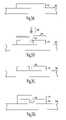
- FIG. 1Ais a cross sectional view of a thermo optic device in the form of an optical waveguide in accordance with the prior art
- FIG. 1Bis a planar view of the thermo optic device of FIG. 1A ;
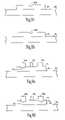
- FIG. 2Ais a cross sectional view of a lower cladding in which a resonator in accordance with the teachings of the present invention will be formed;
- FIG. 2Bis a cross sectional view in accordance with the teachings of the present invention of a first photomasking step in a processing step subsequent to FIG. 2A ;
- FIG. 2Cis a cross sectional view in accordance with the teachings of the present invention of a depression formed in a lower cladding in a processing step subsequent to FIG. 2B ;
- FIG. 2Dis a cross sectional view in accordance with the teachings of the present invention of a layer deposited on the lower cladding in a processing step subsequent to FIG. 2C ;
- FIG. 2Eis a cross sectional view in accordance with the teachings of the present invention of a second photomasking step in a processing step subsequent to FIG. 2D ;
- FIG. 2Fis a cross sectional view in accordance with the teachings of the present invention of a patterned resonator and waveguides in a processing step subsequent to FIG. 2E ;
- FIG. 2Gis a cross sectional view in accordance with the teachings of the present invention of a resonator and waveguides covered by an upper cladding thereby forming a thermo optic device in a processing step subsequent to FIG. 2F ;
- FIG. 3Ais a cross sectional view in accordance with the teachings of the present invention of another embodiment of a depression in a lower cladding;
- FIG. 3Bis a cross sectional view in accordance with the teachings of the present invention of still another embodiment of a depression in a lower cladding;
- FIG. 4Ais a cross sectional view in accordance with the teachings of the present invention of an input waveguide formed in a depression of a lower cladding;
- FIG. 4Bis a cross sectional view in accordance with the teachings of the present invention of an input and output waveguide formed in depressions of a lower cladding;
- FIG. 5is a cross sectional view in accordance with the teachings of the present invention of a plurality of resonators formed in a plurality of depressions of a lower cladding;
- FIG. 6is a perspective view in accordance with the teachings of the present invention of a depression formed across a lower cladding
- FIG. 7is a perspective view of an alternative embodiment of a plurality of depressions formed in a lower cladding
- FIG. 8is a perspective view in accordance with the teachings of the present invention of a depression pattern formed in a lower cladding
- FIG. 9is a perspective view in accordance with the teachings of the present invention of a plurality of regions of the lower cladding having depressions formed therein;
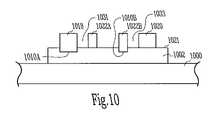
- FIG. 10is a cross sectional view in accordance with the teachings of the present invention of a waveguide and a resonator formed in a plurality of depressions of the lower cladding;
- FIG. 11is a block diagram of a system having a thermo optic package comprising resonators formed in accordance with the teachings of the present invention.
- FIG. 12is an alternative embodiment of a thermo optic package comprising resonators formed in accordance with the teachings of the present invention.
- substrate used in this specificationincludes any base semiconductor structure such as silicon-on-sapphire (SOS) technology, silicon-on-insulator (SOI) technology, thin film transistor (TFT) technology, doped and undoped semiconductors, epitaxial layers of a silicon supported by a base semiconductor structure, as well as other semiconductor structures well known to one skilled in the art.
- SOSsilicon-on-sapphire
- SOIsilicon-on-insulator
- TFTthin film transistor
- doped and undoped semiconductorsepitaxial layers of a silicon supported by a base semiconductor structure, as well as other semiconductor structures well known to one skilled in the art.
- the lower cladding of a thermo optic device of the present inventionhas a reference number of 202 , 302 , 402 , etc. corresponding to the lower cladding X 02 in FIGS. 2 , 3 , 4 , etc. where X is the number of the figure in which the reference numeral appears.
- a substrate 200is provided upon which a resonator for use with a thermo optic device will be formed.
- the substrateis silicon.
- itis a printed circuit board.
- itis any surface upon which a layer may be deposited.
- a first layer 202 or lower claddingis formed on the substrate.
- the substrateis some form of silicon and the first layer is formed as a grown layer via oxidation of the substrate.
- the first layeris formed by deposition techniques.
- Some particular deposition techniques for the first layer, and all remaining deposited layersinclude, but are not limited to, any variety of chemical vapor depositions (CVD), physical vapor depositions (PVD), epitaxy, evaporation, sputtering or other known or hereinafter developed techniques.
- CVD techniquesinclude low pressure (LP) ones, but could also be atmospheric pressure (AP), plasma enhanced (PE), high density plasma (HDP) or other.
- the first layeris a silicon oxide that is deposited via a LPCVD technique using a tetraethyl orthosilicate or TEOS source.
- a first mask 204is provided to photo impact 206 the first layer 202 in a photomasking step so that a photo impacted region 208 is formed in the lower cladding.
- the photo impactingis accomplished with an ultraviolet light from a photolithography device well known to those skilled in the art.
- the photo impactingshould not be limited to such an embodiment and may alternatively include X-rays or other light sources.
- the first mask 204may be configured as a clear-field or dark-field mask, as those terms as well understood by skilled artisans, according to the desired design of the photo impacted region 208 in the lower cladding.
- the first layer 202is etched so that the photo impacted region 208 is removed thereby leaving or forming a depression 210 in the lower cladding.
- the depression 210is shaped as a trench but it may also comprise other shapes, such as a concavity 310 A ( FIG. 3A ), an angular indentation 310 B ( FIG. 3 b ) or other.
- the depression 210is depicted in a cross sectional view it also has a lengthwise dimension (into or away from the paper) and it may be formed completely across the surface of the lower cladding or may be formed in just a particular region thereof.
- the depressionis formed as a trench 610 across an entire surface 621 of lower cladding 602 .
- the depressionis formed as a plurality of concavities 710 in only various regions of surface 721 of lower cladding 702 .
- the depressionmay take on a desired pattern or shape across the lower cladding or in just a particular region.
- the depressionis formed as a trench 810 extending lengthwise across surface 821 of the lower cladding 802 .
- the trench 810has a bend 811 representative of at least one depression pattern.
- the depression of the lower cladding 902is represented as a plurality of concavities 910 having a generally cube shape that is formed in various specific or random regions of surface 921 .
- depressionsare formable in the lower cladding and include, but are not limited to rectangles, circles, serpentine formations, tooth-shaped patterns, polygons, triangles, squares, or any other geometric shape(s) that could be fabricated with the first mask. It should be further appreciated that the particularly shown trenches, concavities, and angular indentations may be of various dimensions and take on any or all embodiments shown herein.
- some etching techniques embraced by this invention for removing the photo impacted region 208 from the lower cladding 202 to form depression 210include, but are not limited to, any variety of wet etches including immersion or spray, or dry etches including plasma, barrel or planar, ion milling, reactive ion etches (RIE) or deep RIE.
- wet etchesincluding immersion or spray, or dry etches including plasma, barrel or planar, ion milling, reactive ion etches (RIE) or deep RIE.
- RIEreactive ion etches
- the photo impacted region 208is dry etched with a photo resist pattern and CF 4 or CF 4 CHF 3 Argon based chemistry in a parallel plate reactor for 360 seconds under the conditions of about 50 militorr, 600 watts and 13.56 MHz.
- a second layer 212is formed on the surface of the first layer 202 in such a manner to “fill” the depression 210 and cover the lower cladding as shown.
- the second layeris a silicon oxynitride deposited with a PECVD technique using a silane with nitrous oxide reaction in an argon or helium plasma for 180 seconds, under the conditions of 400° C., 450 watts and 13.56 MHz.
- the second layeris a translucent material.
- the lower claddingin one embodiment, was formed of a silicon oxide and the second layer was formed of silicon oxynitride, it should be appreciated that numerous other materials for these first and second layers exist. What dictates the selection of the materials is the index of refraction. This is because the second layer will be formed into the waveguide and resonator and light will be propagated therein via reflections of light that occur at the boundary where the two layers meet. So long as the second layer is a material having an index of refraction that is different, either higher or lower, than the index of refraction for the first layer (at whatever wavelength of light the thermo optic device is designed for) light signals can be propagated.
- a second mask 214is provided to photo impact 216 the second layer 212 in another photomasking step.
- the photo impactingis accomplished with an ultraviolet light from a photolithography device but may alternatively include X-rays or other light sources.
- the second maskbe configured in such a way that the photo impacted region of the second layer takes on a desired form such as those previously shown.
- Some particular mask embodimentsinclude, but are not limited to, clear-field or dark-field masks.
- the photo impacted region 209 of the second layer 212 caused by photo impacting 216is etched away thereby forming a resonator 222 and at least one waveguide.
- the waveguideis an optical waveguide having an input waveguide 218 and an output waveguide 220 on either sides of the resonator.
- the resonator 222has a portion thereof, having a depth “D,” formed in the depression between surface 221 of first layer 202 and depression bottom 223 . It has another portion thereof formed between surface 221 and plane 225 . Simultaneously, the waveguides 218 , 220 have no portion thereof formed in the depression and all portions thereof formed on the surface 221 of the first layer and extending from the surface 221 to plane 225 . As a result, the aspect ratio between the resonator and the waveguides has decreased (in comparison to the prior art, FIG. 1A , for example) thereby increasing resonator bandwidth.
- the aspect ratio between adjacent resonatorsFIG. 5 , 522 A and 522 B also decreases which also helps with easier processing for the top cladding layer.
- the aspect ratiodecreased so significantly that the resonator bandwidth approximately doubled by increasing from about 16 nm to about 32 nm.
- the depth “d” to which the resonator is formed in or fills the depressionis dictated by at least two factors.
- the firstis a practical limitation governed by the fill capability inherent in the material of the second layer. For example, if the second layer were deposited as a liquid (amorphous), and the depth of the depression was a relatively substantial percentage of the thickness of the lower cladding, it would likely fill to a greater depth than a non-liquid.
- the depthis a function of the frequency gain the designed resonator is trying to achieve and varies greatly from application to application.
- the height of the resonator between surface 221 and plane 225is not required to be any particular height and is dictated according to the frequency characteristics demanded by the particular application in which the resonator is used. As a reference point, however, resonator and waveguide height is often in a range from about 1 to about 2 microns.
- the horizontal spacing between the resonators and the waveguidesis not required to be any particular distance and is dictated according to the frequency characteristics demanded by the particular application in which the resonator is used. As a reference point, however, horizontal spacing between resonators and waveguides is often in a range from about 1 to about 2 microns.
- the upper surfaces of the input and output waveguides 218 , 220 and resonator 222are all substantially coplanar as defined by plane 225 (although only shown in one dimension). As a result, the manufacturing of a resonator having an increased bandwidth is completed after the etching process performed on the second layer and no additional processing steps need to occur.
- a third layer 224 or upper claddingis deposited on the waveguides 218 , 220 , the resonator 222 and portions 235 of the lower cladding not having a waveguide or resonator.
- the upper claddingis deposited to a thickness sufficient to prevent outside light from interfering with the light propagated in the waveguide during use.
- thickness for both the upper and lower claddingsis often the same and in one embodiment is about 4 microns nominally.
- the third layeris a second silicon oxide layer deposited in the same manner as previously described for the first layer.
- the third layerhas an index of refraction that is substantially equal to the index of refraction of the first layer.
- the third layer 224has an upper surface 226 that can be used to stack multiple thermo optic devices by continuing the deposition, patterning and etching processes described herein.
- the surface 226may alternatively contain a heater (not shown) for changing a thermo optical property of the device as light propagates in the waveguide during use.
- thermo optic devices of the present inventionmay be formed with a more than a single resonator.
- a plurality of resonators, first and second resonators 522 A and 522 Bare formed in a corresponding number of depressions, first and second depressions 510 A and 510 B, while first and second waveguides, input and output waveguides 518 , 520 are formed on the surface 521 of the lower cladding.
- the horizontal spacing between adjacent resonatorsis in a range from about 2 to about 3 microns while the horizontal width of the resonator is about 2 microns nominally. In this manner, even further variations in the frequency characteristics of the resonator can be achieved as application demand varies.
- a first waveguide, input waveguide 418 Ais formed in a depression 410 while resonator 422 is formed on the surface 421 of the lower cladding 402 .
- a first and second waveguide, input and output waveguides 418 B, 420 Bare formed in depressions 410 while the resonator 422 is formed on surface 421 of the lower cladding 402 .
- waveguide 1018is formed in a first depression 1010 A while a first resonator, resonator 1022 A, is formed on the surface 1021 of the lower cladding 1002 . Accordingly, the aspect ratio in area 1031 is increased as between waveguide 1018 and resonator 1022 A, thereby decreasing bandwidth of resonator 1022 A.
- Waveguide 1020is formed on the surface 1021 while a second resonator, resonator 1022 B, is formed in depression 1010 B of the lower cladding. Accordingly, the aspect ratio in area 1033 is decreased as between waveguide 1022 and resonator 1022 B, thereby increasing bandwidth of resonator 1022 B.
- thermo optic devicemay be an amplifier, modulator, gate, filter, time delay element, switch, multiplexer, or other.
- a systemhaving as part thereof a resonator or waveguide formed in accordance with the teachings of the present invention, is shown generally as 1141 .
- the systemmay be an exclusively fiber optic system or may be a system having other software and hardware devices, as indicated by the dashed line 1145 , operably coupled to at least one fiber optic component thereof.
- a light source 1143will be provided as the source for propagating light signals along at least one fiber optic line 1147 .
- Well known light sourcesinclude, but are not limited to, laser light sources.
- the system 1141includes a plurality of fiber optic lines 1147 .
- thermo optic package 1149Contained within the thermo optic package is at least one thermo optic device 1153 having at least one resonator or waveguide formed in accordance with the present invention.
- the thermo optic device 1153is coupled to the input fiber optic port 1151 via an input connector 1155 while an output connector 1157 couples the thermo optic device to an output fiber optic port 1159 .
- the output fiber optic port 1159is coupled to another fiber optic line 1147 of system 1141 .
- a system usermerely needs to couple fiber optic lines 1147 to the input and output fiber optic ports of the package 1149 to readily achieve at least one resonator or waveguide having an increased or decreased bandwidth as necessary.
- thermo optic package 1249having a thermo optic device 1253 with a single input connector 1255 and a plurality of output connectors 1257 .
- the input connector 1255connects with input fiber optic port 1251 which is readily matable with a fiber optic line 1247 of a system.
- the output connectors 1257 of thermo optic device 1253are each matable with an output fiber optic port 1259 .
- the single input connector of the thermo optic device 1253having a resonator or waveguide formed in accordance with the present invention, may alternatively be replaced with two or more input connectors while the two output connectors may be replaced with one or more output connectors depending upon the type and desired use of the thermo optic device 1253 .
- thermo optic deviceshave been described, by way of example, and not by way of limitation, with respect to resonators for thermo optic devices.
- the resonator of a thermo optic deviceis formed in the same process steps as a waveguide and is formed in a depression of a lower cladding while the waveguide is formed on a surface of the lower cladding.
- the aspect ratio as between the waveguide and resonator in an area where the waveguide and resonator front or face one anotherdecreases thereby increasing the bandwidth of the resonator.
- the depressionis formed by photomasking and etching the lower cladding before forming the resonator and waveguide. Some depression embodiments include trenches, concavities and angular indentations.
- a plurality of resonatorsare taught that are formed in a plurality of depressions of the lower cladding while a plurality of waveguides are formed on the surface of the lower cladding.
- waveguide(s)are formed in the depression(s) of the lower cladding while the resonator is formed on the surface. In this manner, the aspect ratio increases thereby decreasing bandwidth of the resonator.
- Thermo optic devices formed with these resonatorsare also taught.
- resonators of this inventioncan be formed quicker and cheaper without any corresponding sacrifice in quality, reliability or longevity.
Landscapes
- Physics & Mathematics (AREA)
- General Physics & Mathematics (AREA)
- Optics & Photonics (AREA)
- Engineering & Computer Science (AREA)
- Microelectronics & Electronic Packaging (AREA)
- Nonlinear Science (AREA)
- Optical Integrated Circuits (AREA)
- Optical Modulation, Optical Deflection, Nonlinear Optics, Optical Demodulation, Optical Logic Elements (AREA)
Abstract
Description
Claims (65)
Priority Applications (4)
| Application Number | Priority Date | Filing Date | Title |
|---|---|---|---|
| US10/231,897US7120336B2 (en) | 2002-08-29 | 2002-08-29 | Resonator for thermo optic device |
| US11/493,717US7323353B2 (en) | 2002-08-29 | 2006-07-26 | Resonator for thermo optic device |
| US11/951,796US8195020B2 (en) | 2002-08-29 | 2007-12-06 | Resonator for thermo optic device |
| US13/483,542US9042697B2 (en) | 2002-08-29 | 2012-05-30 | Resonator for thermo optic device |
Applications Claiming Priority (1)
| Application Number | Priority Date | Filing Date | Title |
|---|---|---|---|
| US10/231,897US7120336B2 (en) | 2002-08-29 | 2002-08-29 | Resonator for thermo optic device |
Related Child Applications (1)
| Application Number | Title | Priority Date | Filing Date |
|---|---|---|---|
| US11/493,717ContinuationUS7323353B2 (en) | 2002-08-29 | 2006-07-26 | Resonator for thermo optic device |
Publications (2)
| Publication Number | Publication Date |
|---|---|
| US20040057687A1 US20040057687A1 (en) | 2004-03-25 |
| US7120336B2true US7120336B2 (en) | 2006-10-10 |
Family
ID=31990396
Family Applications (4)
| Application Number | Title | Priority Date | Filing Date |
|---|---|---|---|
| US10/231,897Expired - Fee RelatedUS7120336B2 (en) | 2002-08-29 | 2002-08-29 | Resonator for thermo optic device |
| US11/493,717Expired - Fee RelatedUS7323353B2 (en) | 2002-08-29 | 2006-07-26 | Resonator for thermo optic device |
| US11/951,796Expired - Fee RelatedUS8195020B2 (en) | 2002-08-29 | 2007-12-06 | Resonator for thermo optic device |
| US13/483,542Expired - Fee RelatedUS9042697B2 (en) | 2002-08-29 | 2012-05-30 | Resonator for thermo optic device |
Family Applications After (3)
| Application Number | Title | Priority Date | Filing Date |
|---|---|---|---|
| US11/493,717Expired - Fee RelatedUS7323353B2 (en) | 2002-08-29 | 2006-07-26 | Resonator for thermo optic device |
| US11/951,796Expired - Fee RelatedUS8195020B2 (en) | 2002-08-29 | 2007-12-06 | Resonator for thermo optic device |
| US13/483,542Expired - Fee RelatedUS9042697B2 (en) | 2002-08-29 | 2012-05-30 | Resonator for thermo optic device |
Country Status (1)
| Country | Link |
|---|---|
| US (4) | US7120336B2 (en) |
Cited By (12)
| Publication number | Priority date | Publication date | Assignee | Title |
|---|---|---|---|---|
| US20050025424A1 (en)* | 2002-08-29 | 2005-02-03 | Micron Technology, Inc. | Resistive heater for thermo optic device |
| US20060263027A1 (en)* | 2002-08-29 | 2006-11-23 | Micron Technology, Inc. | Resonator for thermo optic device |
| US7359607B2 (en) | 2002-08-29 | 2008-04-15 | Micron Technology, Inc. | Waveguide for thermo optic device |
| US20090238526A1 (en)* | 2003-03-04 | 2009-09-24 | Lucent Technologies Inc. | Optical transmission fiber with thermal management for high power applications |
| US20100054653A1 (en)* | 2008-08-29 | 2010-03-04 | Bae Systems Information And Electronic Systems Integration Inc. | Salicide structures for heat-influenced semiconductor applications |
| US20120138568A1 (en)* | 2010-12-07 | 2012-06-07 | Na Yun-Chung N | Low-cost passive optical waveguide using si substrate |
| US9465163B2 (en)* | 2014-03-07 | 2016-10-11 | Skorpios Technologies, Inc. | High-order-mode filter for semiconductor waveguides |
| US20170090118A1 (en)* | 2014-03-07 | 2017-03-30 | Skorpios Technologies, Inc. | Wide shoulder, high order mode filter for thick-silicon waveguides |
| US9885832B2 (en) | 2014-05-27 | 2018-02-06 | Skorpios Technologies, Inc. | Waveguide mode expander using amorphous silicon |
| US9977188B2 (en) | 2011-08-30 | 2018-05-22 | Skorpios Technologies, Inc. | Integrated photonics mode expander |
| US10649148B2 (en) | 2017-10-25 | 2020-05-12 | Skorpios Technologies, Inc. | Multistage spot size converter in silicon photonics |
| US11360263B2 (en) | 2019-01-31 | 2022-06-14 | Skorpios Technologies. Inc. | Self-aligned spot size converter |
Families Citing this family (1)
| Publication number | Priority date | Publication date | Assignee | Title |
|---|---|---|---|---|
| US9684191B2 (en) | 2015-11-05 | 2017-06-20 | International Business Machines Corporation | Efficient thermo-optic phase shifters using multi-pass heaters |
Citations (41)
| Publication number | Priority date | Publication date | Assignee | Title |
|---|---|---|---|---|
| US4166669A (en) | 1977-05-13 | 1979-09-04 | Massachusetts Institute Of Technology | Planar optical waveguide, modulator, variable coupler and switch |
| US4518219A (en) | 1980-01-25 | 1985-05-21 | Massachusetts Institute Of Technology | Optical guided wave devices employing semiconductor-insulator structures |
| US4799749A (en)* | 1985-02-25 | 1989-01-24 | Siemens Aktiengesellschaft | Integrated resonator matrix for wavelength-selective separation or joining of channels in the frequency domain of optical communications technology |
| US4886538A (en) | 1987-07-28 | 1989-12-12 | Polaroid Corporation | Process for tapering waveguides |
| US5639386A (en) | 1992-11-05 | 1997-06-17 | Xerox Corporation | Increased threshold uniformity of thermal ink transducers |
| US5710849A (en)* | 1995-11-01 | 1998-01-20 | Northern Telecom, Ltd. | Taper shapes for flatband response and sidelobe suppression in grating assisted optical coupler filters |
| US5841931A (en) | 1996-11-26 | 1998-11-24 | Massachusetts Institute Of Technology | Methods of forming polycrystalline semiconductor waveguides for optoelectronic integrated circuits, and devices formed thereby |
| US5987196A (en) | 1997-11-06 | 1999-11-16 | Micron Technology, Inc. | Semiconductor structure having an optical signal path in a substrate and method for forming the same |
| US6035089A (en) | 1997-06-11 | 2000-03-07 | Lockheed Martin Energy Research Corporation | Integrated narrowband optical filter based on embedded subwavelength resonant grating structures |
| US6052495A (en) | 1997-10-01 | 2000-04-18 | Massachusetts Institute Of Technology | Resonator modulators and wavelength routing switches |
| US6090636A (en) | 1998-02-26 | 2000-07-18 | Micron Technology, Inc. | Integrated circuits using optical waveguide interconnects formed through a semiconductor wafer and methods for forming same |
| US6097865A (en) | 1998-07-21 | 2000-08-01 | Lucent Technologies Inc. | Design and method for planar coupled waveguide filter |
| US6101300A (en)* | 1997-06-09 | 2000-08-08 | Massachusetts Institute Of Technology | High efficiency channel drop filter with absorption induced on/off switching and modulation |
| US6144779A (en) | 1997-03-11 | 2000-11-07 | Lightwave Microsystems Corporation | Optical interconnects with hybrid construction |
| US6150188A (en) | 1998-02-26 | 2000-11-21 | Micron Technology Inc. | Integrated circuits using optical fiber interconnects formed through a semiconductor wafer and methods for forming same |
| US6219366B1 (en) | 1997-05-02 | 2001-04-17 | Nec Corporation | Semiconductor optical device and method of manufacturing the same |
| US6278168B1 (en) | 1998-07-17 | 2001-08-21 | Bookham Technology Plc | Thermo-optic semiconductor device |
| US20010026670A1 (en) | 2000-03-28 | 2001-10-04 | Matsushita Electric Industrial Co., Ltd. | Optical waveguide and method for making the same |
| US6311004B1 (en) | 1998-11-10 | 2001-10-30 | Lightwave Microsystems | Photonic devices comprising thermo-optic polymer |
| US20010046363A1 (en) | 2000-03-03 | 2001-11-29 | Purchase Ken G. | Variable optical attenuators and optical shutters using a coupling layer in proximity to an optical waveguide (II) |
| US20020018634A1 (en) | 1998-02-02 | 2002-02-14 | Tsuguhiro Korenaga | Optical waveguide component and a method of producing the same |
| US6396988B1 (en)* | 1999-08-13 | 2002-05-28 | Nec Corporation | Optical waveguide device and method of forming the same |
| US6411752B1 (en)* | 1999-02-22 | 2002-06-25 | Massachusetts Institute Of Technology | Vertically coupled optical resonator devices over a cross-grid waveguide architecture |
| US6433919B1 (en)* | 2000-05-19 | 2002-08-13 | Wisconsin Alumni Research Foundation | Method and apparatus for wavelength conversion and switching |
| US6453377B1 (en) | 1998-06-16 | 2002-09-17 | Micron Technology, Inc. | Computer including optical interconnect, memory unit, and method of assembling a computer |
| US20020186920A1 (en) | 1999-10-28 | 2002-12-12 | Jean-Francois Viens | Coupler assisted tunable add/drop filter |
| US20030026575A1 (en)* | 2001-08-02 | 2003-02-06 | Motorola, Inc. | Structure and method for fabricating semiconductor optical waveguide structures utilizing the formation of a compliant substrate |
| US6522812B1 (en) | 2001-12-19 | 2003-02-18 | Intel Corporation | Method of precision fabrication by light exposure and structure of tunable waveguide bragg grating |
| US6532326B1 (en)* | 2000-09-21 | 2003-03-11 | Ut-Battelle, Llc | Transverse-longitudinal integrated resonator |
| US6567573B1 (en)* | 1997-02-12 | 2003-05-20 | Digilens, Inc. | Switchable optical components |
| US6571039B1 (en) | 1999-11-23 | 2003-05-27 | Lnl Technologies, Inc. | Optical waveguide having a weakly-confining waveguide section and a strongly-confining waveguide section optically coupled by a tapered neck |
| US6573813B1 (en) | 1999-04-23 | 2003-06-03 | Massachusetts Institute Of Technology | All-dielectric coaxial waveguide with annular sections |
| US20030169964A1 (en) | 2002-03-08 | 2003-09-11 | Tairan Wang | Power splitter/combiner with parameter tolerance and design process therefor |
| US20030174956A1 (en) | 2002-03-13 | 2003-09-18 | Jean-Francois Viens | Polarization insensitive modal field transformer for high index contrast waveguide devices |
| US20030174946A1 (en) | 2002-03-14 | 2003-09-18 | Jean-Francois Viens | Superstructure photonic band-gap grating add-drop filter |
| US20030174945A1 (en) | 2002-03-12 | 2003-09-18 | Fried Dale G. | Periodic electromagnetic waveguide structures with controlled polarization properties |
| US20030202548A1 (en)* | 2002-04-26 | 2003-10-30 | Andersen John Kai | Semiconductor micro-resonator for monitoring an optical device |
| US20040037341A1 (en)* | 2002-08-21 | 2004-02-26 | Tan Michael R. | Laser utilizing a microdisk resonator |
| US6748138B2 (en) | 2001-09-14 | 2004-06-08 | Fibera, Inc. | Optical grating fabrication |
| US20050025424A1 (en) | 2002-08-29 | 2005-02-03 | Micron Technology, Inc. | Resistive heater for thermo optic device |
| US20050031284A1 (en) | 2002-08-29 | 2005-02-10 | Micron Technology, Inc., Clarendon Photonics | Waveguide for thermo optic device |
Family Cites Families (39)
| Publication number | Priority date | Publication date | Assignee | Title |
|---|---|---|---|---|
| US3589794A (en) | 1968-08-07 | 1971-06-29 | Bell Telephone Labor Inc | Optical circuits |
| DE2706755C2 (en)* | 1977-02-17 | 1983-12-22 | Dynamit Nobel Ag, 5210 Troisdorf | Method and device for incorporating glass fibers into thermoplastics |
| US4616898A (en) | 1980-03-31 | 1986-10-14 | Polaroid Corporation | Optical communication systems using raman repeaters and components therefor |
| US4592043A (en) | 1983-07-08 | 1986-05-27 | At&T Bell Laboratories | Wavelength division multiplexing optical communications systems |
| DE3329719A1 (en) | 1983-08-17 | 1985-03-07 | Siemens Ag | PHOTODIOD WITH RESONATOR STRUCTURE FOR INCREASING ABSORPTION |
| EP0233896B1 (en) | 1985-07-24 | 1990-08-22 | BRITISH TELECOMMUNICATIONS public limited company | Dielectric optical waveguide device |
| US5155620A (en) | 1991-06-19 | 1992-10-13 | At&T Bell Laboratories | Nonlinear optical devices and methods |
| GB9225273D0 (en) | 1992-12-03 | 1993-01-27 | Int Computers Ltd | Electronic circuit assemblies |
| EP0631159A1 (en) | 1993-06-18 | 1994-12-28 | Siemens Aktiengesellschaft | Coupling between a planar optical waveguide and an optical fibre and fabrication method for an appropiate planar waveguide |
| US5784400A (en) | 1995-02-28 | 1998-07-21 | Massachusetts Institute Of Technology | Resonant cavities employing two dimensionally periodic dielectric materials |
| IL119006A (en)* | 1996-08-04 | 2001-04-30 | B G Negev Technologies And App | Tunable delay line optical filters |
| US5838845A (en)* | 1996-09-09 | 1998-11-17 | Lucent Technologies Inc. | Primary stage optical switch assembly for an optical fiber administration system |
| US5915051A (en) | 1997-01-21 | 1999-06-22 | Massascusetts Institute Of Technology | Wavelength-selective optical add/drop switch |
| US6022671A (en) | 1997-03-11 | 2000-02-08 | Lightwave Microsystems Corporation | Method of making optical interconnects with hybrid construction |
| JP3259765B2 (en)* | 1997-12-11 | 2002-02-25 | 住友電気工業株式会社 | Optical input / output module and optical reflector |
| JP4652507B2 (en) | 1998-12-25 | 2011-03-16 | 古河電気工業株式会社 | Optical waveguide circuit and manufacturing method thereof |
| WO2001022139A1 (en)* | 1999-09-21 | 2001-03-29 | Nanovation Technologies, Inc. | Channel-dropping filter having two resonators for coupling the two polarisation componants |
| US6393185B1 (en)* | 1999-11-03 | 2002-05-21 | Sparkolor Corporation | Differential waveguide pair |
| US20040114899A1 (en)* | 2000-02-16 | 2004-06-17 | Mattsson Kent Erick | Planar, integrated, optical, air-clad waveguide and method of producing same |
| US6865314B1 (en) | 2001-01-11 | 2005-03-08 | Steven M. Blair | Tunable optical wavelength filters and multi-level optical integrated circuits |
| JP2002353703A (en)* | 2001-03-19 | 2002-12-06 | Tdk Corp | Band pass filter |
| JP2002329369A (en) | 2001-04-27 | 2002-11-15 | Sony Corp | Optical disk and optical disk device |
| US20030033975A1 (en) | 2001-08-17 | 2003-02-20 | Michael Bazylenko | Method of forming a planar waveguide core |
| US6744953B2 (en)* | 2001-09-07 | 2004-06-01 | Agilent Technologies, Inc. | Planar optical waveguide with alignment structure |
| US20030048501A1 (en) | 2001-09-12 | 2003-03-13 | Michael Guess | Metropolitan area local access service system |
| JP2003172841A (en)* | 2001-09-28 | 2003-06-20 | Omron Corp | Optical waveguide and method of manufacturing the same |
| US20030123827A1 (en)* | 2001-12-28 | 2003-07-03 | Xtalight, Inc. | Systems and methods of manufacturing integrated photonic circuit devices |
| JP2003240997A (en) | 2002-02-21 | 2003-08-27 | Fujitsu Ltd | Method for manufacturing optical integrated circuit having space reflection type structure |
| US7184669B2 (en)* | 2002-04-26 | 2007-02-27 | Avago Technologies Fiber Ip (Singapore) Pte. Ltd. | Optical transceiver systems and methods |
| US6832034B2 (en)* | 2002-06-21 | 2004-12-14 | 3M Innovative Properties Company | Optical waveguide |
| US20040001665A1 (en)* | 2002-07-01 | 2004-01-01 | Majd Zoorob | Optical device |
| US6975798B2 (en) | 2002-07-05 | 2005-12-13 | Xponent Photonics Inc | Waveguides assembled for transverse-transfer of optical power |
| US20040008968A1 (en)* | 2002-07-09 | 2004-01-15 | L3 Optics, Inc. | Photosensitive optical glass |
| US6950581B2 (en) | 2002-07-22 | 2005-09-27 | Intel Corporation | Optical coupler apparatus and methods having reduced geometry sensitivity |
| US7120336B2 (en) | 2002-08-29 | 2006-10-10 | Micron Technology, Inc. | Resonator for thermo optic device |
| US7088919B2 (en) | 2002-11-04 | 2006-08-08 | Nortel Networks Limited | Modular photonic switch with wavelength conversion |
| KR100506311B1 (en) | 2003-01-20 | 2005-08-05 | 삼성전자주식회사 | Wide-band dispersion controlled optical fiber |
| KR100678222B1 (en) | 2004-02-07 | 2007-02-01 | 삼성전자주식회사 | Optical fiber for metro networks |
| KR100651506B1 (en) | 2004-05-13 | 2006-11-29 | 삼성전자주식회사 | Optical fiber for long distance optical network |
- 2002
- 2002-08-29USUS10/231,897patent/US7120336B2/ennot_activeExpired - Fee Related
- 2006
- 2006-07-26USUS11/493,717patent/US7323353B2/ennot_activeExpired - Fee Related
- 2007
- 2007-12-06USUS11/951,796patent/US8195020B2/ennot_activeExpired - Fee Related
- 2012
- 2012-05-30USUS13/483,542patent/US9042697B2/ennot_activeExpired - Fee Related
Patent Citations (49)
| Publication number | Priority date | Publication date | Assignee | Title |
|---|---|---|---|---|
| US4166669A (en) | 1977-05-13 | 1979-09-04 | Massachusetts Institute Of Technology | Planar optical waveguide, modulator, variable coupler and switch |
| US4518219A (en) | 1980-01-25 | 1985-05-21 | Massachusetts Institute Of Technology | Optical guided wave devices employing semiconductor-insulator structures |
| US4799749A (en)* | 1985-02-25 | 1989-01-24 | Siemens Aktiengesellschaft | Integrated resonator matrix for wavelength-selective separation or joining of channels in the frequency domain of optical communications technology |
| US4886538A (en) | 1987-07-28 | 1989-12-12 | Polaroid Corporation | Process for tapering waveguides |
| US5639386A (en) | 1992-11-05 | 1997-06-17 | Xerox Corporation | Increased threshold uniformity of thermal ink transducers |
| US5710849A (en)* | 1995-11-01 | 1998-01-20 | Northern Telecom, Ltd. | Taper shapes for flatband response and sidelobe suppression in grating assisted optical coupler filters |
| US6108464A (en) | 1996-11-26 | 2000-08-22 | Massachusetts Institute Of Technology | Optoelectronic integrated circuits formed of polycrystalline semiconductor waveguide |
| US5841931A (en) | 1996-11-26 | 1998-11-24 | Massachusetts Institute Of Technology | Methods of forming polycrystalline semiconductor waveguides for optoelectronic integrated circuits, and devices formed thereby |
| US6567573B1 (en)* | 1997-02-12 | 2003-05-20 | Digilens, Inc. | Switchable optical components |
| US6144779A (en) | 1997-03-11 | 2000-11-07 | Lightwave Microsystems Corporation | Optical interconnects with hybrid construction |
| US6219366B1 (en) | 1997-05-02 | 2001-04-17 | Nec Corporation | Semiconductor optical device and method of manufacturing the same |
| US6465269B2 (en) | 1997-05-02 | 2002-10-15 | Nec Corporation | Semiconductor optical device and method of manufacturing the same |
| US6101300A (en)* | 1997-06-09 | 2000-08-08 | Massachusetts Institute Of Technology | High efficiency channel drop filter with absorption induced on/off switching and modulation |
| US6035089A (en) | 1997-06-11 | 2000-03-07 | Lockheed Martin Energy Research Corporation | Integrated narrowband optical filter based on embedded subwavelength resonant grating structures |
| US6052495A (en) | 1997-10-01 | 2000-04-18 | Massachusetts Institute Of Technology | Resonator modulators and wavelength routing switches |
| US5987196A (en) | 1997-11-06 | 1999-11-16 | Micron Technology, Inc. | Semiconductor structure having an optical signal path in a substrate and method for forming the same |
| US20020018634A1 (en) | 1998-02-02 | 2002-02-14 | Tsuguhiro Korenaga | Optical waveguide component and a method of producing the same |
| US6090636A (en) | 1998-02-26 | 2000-07-18 | Micron Technology, Inc. | Integrated circuits using optical waveguide interconnects formed through a semiconductor wafer and methods for forming same |
| US6150188A (en) | 1998-02-26 | 2000-11-21 | Micron Technology Inc. | Integrated circuits using optical fiber interconnects formed through a semiconductor wafer and methods for forming same |
| US6526191B1 (en) | 1998-02-26 | 2003-02-25 | Micron Technology, Inc. | Integrated circuits using optical fiber interconnects formed through a semiconductor wafer and methods for forming same |
| US20030197186A1 (en) | 1998-02-26 | 2003-10-23 | Micron Technology, Inc. | Integrated circuits using optical waveguide interconnects formed through a semiconductor wafer and methods for forming same |
| US6519658B2 (en) | 1998-06-16 | 2003-02-11 | Micron Technology, Inc. | Memory unit and method of assembling a computer |
| US6453377B1 (en) | 1998-06-16 | 2002-09-17 | Micron Technology, Inc. | Computer including optical interconnect, memory unit, and method of assembling a computer |
| US6278168B1 (en) | 1998-07-17 | 2001-08-21 | Bookham Technology Plc | Thermo-optic semiconductor device |
| US6097865A (en) | 1998-07-21 | 2000-08-01 | Lucent Technologies Inc. | Design and method for planar coupled waveguide filter |
| US6311004B1 (en) | 1998-11-10 | 2001-10-30 | Lightwave Microsystems | Photonic devices comprising thermo-optic polymer |
| US6411752B1 (en)* | 1999-02-22 | 2002-06-25 | Massachusetts Institute Of Technology | Vertically coupled optical resonator devices over a cross-grid waveguide architecture |
| US6573813B1 (en) | 1999-04-23 | 2003-06-03 | Massachusetts Institute Of Technology | All-dielectric coaxial waveguide with annular sections |
| US6396988B1 (en)* | 1999-08-13 | 2002-05-28 | Nec Corporation | Optical waveguide device and method of forming the same |
| US20020186920A1 (en) | 1999-10-28 | 2002-12-12 | Jean-Francois Viens | Coupler assisted tunable add/drop filter |
| US6571039B1 (en) | 1999-11-23 | 2003-05-27 | Lnl Technologies, Inc. | Optical waveguide having a weakly-confining waveguide section and a strongly-confining waveguide section optically coupled by a tapered neck |
| US20010046363A1 (en) | 2000-03-03 | 2001-11-29 | Purchase Ken G. | Variable optical attenuators and optical shutters using a coupling layer in proximity to an optical waveguide (II) |
| US20010026670A1 (en) | 2000-03-28 | 2001-10-04 | Matsushita Electric Industrial Co., Ltd. | Optical waveguide and method for making the same |
| US6433919B1 (en)* | 2000-05-19 | 2002-08-13 | Wisconsin Alumni Research Foundation | Method and apparatus for wavelength conversion and switching |
| US6532326B1 (en)* | 2000-09-21 | 2003-03-11 | Ut-Battelle, Llc | Transverse-longitudinal integrated resonator |
| US20030026575A1 (en)* | 2001-08-02 | 2003-02-06 | Motorola, Inc. | Structure and method for fabricating semiconductor optical waveguide structures utilizing the formation of a compliant substrate |
| US6748138B2 (en) | 2001-09-14 | 2004-06-08 | Fibera, Inc. | Optical grating fabrication |
| US6522812B1 (en) | 2001-12-19 | 2003-02-18 | Intel Corporation | Method of precision fabrication by light exposure and structure of tunable waveguide bragg grating |
| US20030169964A1 (en) | 2002-03-08 | 2003-09-11 | Tairan Wang | Power splitter/combiner with parameter tolerance and design process therefor |
| US20030174945A1 (en) | 2002-03-12 | 2003-09-18 | Fried Dale G. | Periodic electromagnetic waveguide structures with controlled polarization properties |
| US20030174956A1 (en) | 2002-03-13 | 2003-09-18 | Jean-Francois Viens | Polarization insensitive modal field transformer for high index contrast waveguide devices |
| US20030174946A1 (en) | 2002-03-14 | 2003-09-18 | Jean-Francois Viens | Superstructure photonic band-gap grating add-drop filter |
| US20030202548A1 (en)* | 2002-04-26 | 2003-10-30 | Andersen John Kai | Semiconductor micro-resonator for monitoring an optical device |
| US20040037341A1 (en)* | 2002-08-21 | 2004-02-26 | Tan Michael R. | Laser utilizing a microdisk resonator |
| US20050025424A1 (en) | 2002-08-29 | 2005-02-03 | Micron Technology, Inc. | Resistive heater for thermo optic device |
| US20050031263A1 (en) | 2002-08-29 | 2005-02-10 | Micron Technology, Inc. | Resistive heater for thermo optic device |
| US20050031284A1 (en) | 2002-08-29 | 2005-02-10 | Micron Technology, Inc., Clarendon Photonics | Waveguide for thermo optic device |
| US7020365B2 (en) | 2002-08-29 | 2006-03-28 | Micron Technology, Inc. | Resistive heater for thermo optic device |
| US20060098911A1 (en) | 2002-08-29 | 2006-05-11 | Micron Technology, Inc. | Resistive heater for thermo optic device |
Non-Patent Citations (1)
| Title |
|---|
| Damask, Jay N., "Integrated-Optic Grating-Based Filters for Optical Communication Systems", Doctoral Thesis, Department of Electrical Engineering, Massachusetts Institute of Technology,(May 6, 1996), 143-183. |
Cited By (39)
| Publication number | Priority date | Publication date | Assignee | Title |
|---|---|---|---|---|
| US20110206332A1 (en)* | 2002-08-29 | 2011-08-25 | Blalock Guy T | Waveguide for thermo optic device |
| US20100220958A1 (en)* | 2002-08-29 | 2010-09-02 | Blalock Guy T | Waveguide for thermo optic device |
| US20060098911A1 (en)* | 2002-08-29 | 2006-05-11 | Micron Technology, Inc. | Resistive heater for thermo optic device |
| US20060263027A1 (en)* | 2002-08-29 | 2006-11-23 | Micron Technology, Inc. | Resonator for thermo optic device |
| US7215838B2 (en) | 2002-08-29 | 2007-05-08 | Micron Technology, Inc. | Resistive heater for thermo optic device |
| US7323353B2 (en) | 2002-08-29 | 2008-01-29 | Micron Technology, Inc. | Resonator for thermo optic device |
| US7359607B2 (en) | 2002-08-29 | 2008-04-15 | Micron Technology, Inc. | Waveguide for thermo optic device |
| US20080089647A1 (en)* | 2002-08-29 | 2008-04-17 | Micron Technology, Inc | Resonator for thermo optic device |
| US20080226247A1 (en)* | 2002-08-29 | 2008-09-18 | Micron Technology, Inc. | Waveguide for thermo optic device |
| US7509005B2 (en) | 2002-08-29 | 2009-03-24 | Micron Technology, Inc. | Resistive heater for thermo optic device |
| US7565039B2 (en) | 2002-08-29 | 2009-07-21 | Micron Technology, Inc. | Resistive heater for thermo optic device |
| US9042697B2 (en) | 2002-08-29 | 2015-05-26 | Micron Technology, Inc. | Resonator for thermo optic device |
| US8195020B2 (en) | 2002-08-29 | 2012-06-05 | Micron Technology, Inc. | Resonator for thermo optic device |
| US20050025424A1 (en)* | 2002-08-29 | 2005-02-03 | Micron Technology, Inc. | Resistive heater for thermo optic device |
| US7706647B2 (en) | 2002-08-29 | 2010-04-27 | Micron Technology, Inc. | Resistive heater for thermo optic device |
| US7720341B2 (en) | 2002-08-29 | 2010-05-18 | Micron Technology, Inc. | Waveguide for thermo optic device |
| US8111965B2 (en) | 2002-08-29 | 2012-02-07 | Micron Technology, Inc. | Waveguide for thermo optic device |
| US7936955B2 (en) | 2002-08-29 | 2011-05-03 | Micron Technology, Inc. | Waveguide for thermo optic device |
| US20050031263A1 (en)* | 2002-08-29 | 2005-02-10 | Micron Technology, Inc. | Resistive heater for thermo optic device |
| US8811789B2 (en)* | 2003-03-04 | 2014-08-19 | Alcatel Lucent | Optical transmission fiber with thermal management for high power applications |
| US20090238526A1 (en)* | 2003-03-04 | 2009-09-24 | Lucent Technologies Inc. | Optical transmission fiber with thermal management for high power applications |
| US7693354B2 (en) | 2008-08-29 | 2010-04-06 | Bae Systems Information And Electronic Systems Integration Inc. | Salicide structures for heat-influenced semiconductor applications |
| US20100054653A1 (en)* | 2008-08-29 | 2010-03-04 | Bae Systems Information And Electronic Systems Integration Inc. | Salicide structures for heat-influenced semiconductor applications |
| US20120138568A1 (en)* | 2010-12-07 | 2012-06-07 | Na Yun-Chung N | Low-cost passive optical waveguide using si substrate |
| US8437585B2 (en)* | 2010-12-07 | 2013-05-07 | Intel Corporation | Low-cost passive optical waveguide using Si substrate |
| US9977188B2 (en) | 2011-08-30 | 2018-05-22 | Skorpios Technologies, Inc. | Integrated photonics mode expander |
| US10895686B2 (en) | 2011-08-30 | 2021-01-19 | Skorpios Technologies, Inc. | Integrated photonics mode expander |
| US10295746B2 (en) | 2014-03-07 | 2019-05-21 | Skorpios Technologies, Inc. | Wide shoulder, high order mode filter for thick-silicon waveguides |
| US9465163B2 (en)* | 2014-03-07 | 2016-10-11 | Skorpios Technologies, Inc. | High-order-mode filter for semiconductor waveguides |
| US10088629B2 (en) | 2014-03-07 | 2018-10-02 | Skorpios Technologies, Inc. | Wide shoulder, high order mode filter for thick-silicon waveguides |
| US20170090118A1 (en)* | 2014-03-07 | 2017-03-30 | Skorpios Technologies, Inc. | Wide shoulder, high order mode filter for thick-silicon waveguides |
| US9664855B2 (en)* | 2014-03-07 | 2017-05-30 | Skorpios Technologies, Inc. | Wide shoulder, high order mode filter for thick-silicon waveguides |
| US10001600B2 (en) | 2014-05-27 | 2018-06-19 | Skorpios Technologies, Inc. | Waveguide mode expander having an amorphous-silicon shoulder |
| US9885832B2 (en) | 2014-05-27 | 2018-02-06 | Skorpios Technologies, Inc. | Waveguide mode expander using amorphous silicon |
| US10345521B2 (en) | 2014-05-27 | 2019-07-09 | Skorpios Technologies, Inc. | Method of modifying mode size of an optical beam, using a waveguide mode expander having non-crystalline silicon features |
| US11409039B2 (en) | 2014-05-27 | 2022-08-09 | Skorpios Technologies, Inc. | Waveguide mode expander having non-crystalline silicon features |
| US10649148B2 (en) | 2017-10-25 | 2020-05-12 | Skorpios Technologies, Inc. | Multistage spot size converter in silicon photonics |
| US11079549B2 (en) | 2017-10-25 | 2021-08-03 | Skorpios Technologies, Inc. | Multistage spot size converter in silicon photonics |
| US11360263B2 (en) | 2019-01-31 | 2022-06-14 | Skorpios Technologies. Inc. | Self-aligned spot size converter |
Also Published As
| Publication number | Publication date |
|---|---|
| US8195020B2 (en) | 2012-06-05 |
| US7323353B2 (en) | 2008-01-29 |
| US20120237165A1 (en) | 2012-09-20 |
| US9042697B2 (en) | 2015-05-26 |
| US20080089647A1 (en) | 2008-04-17 |
| US20040057687A1 (en) | 2004-03-25 |
| US20060263027A1 (en) | 2006-11-23 |
Similar Documents
| Publication | Publication Date | Title |
|---|---|---|
| US7323353B2 (en) | Resonator for thermo optic device | |
| US7720341B2 (en) | Waveguide for thermo optic device | |
| US6571039B1 (en) | Optical waveguide having a weakly-confining waveguide section and a strongly-confining waveguide section optically coupled by a tapered neck | |
| US20080205838A1 (en) | Optical Device Including a Buried Grating With Air Filled Voids and Method For Realising It | |
| US6921490B1 (en) | Optical component having waveguides extending from a common region | |
| CN114460681A (en) | Waveguide intersection including segmented waveguide segments | |
| US20030052082A1 (en) | Method of forming optical waveguides in a semiconductor substrate | |
| CN112230339A (en) | Grating coupler and preparation method thereof | |
| JP3613413B2 (en) | Method for producing waveguide Bragg reflector and product obtained | |
| US6732550B2 (en) | Method for performing a deep trench etch for a planar lightwave circuit | |
| US20040126051A1 (en) | Low-birefringent integrated optics structures | |
| TW202346974A (en) | Vertical grating filters for photonics and method of forming the same | |
| US10746925B2 (en) | Silicon nitride grating couplers | |
| KR100394019B1 (en) | method for production of optical communication type coupler element | |
| US20050211664A1 (en) | Method of forming optical waveguides in a semiconductor substrate | |
| US20250224566A1 (en) | Semiconductor photonics device and methods of formation | |
| KR100394018B1 (en) | method for production of optical communication type optical super prism | |
| KR100591766B1 (en) | Method for manufacturing silica flat optical waveguide with integrated mode size matcher | |
| JP2001201647A (en) | Optical waveguide circuit and method of manufacturing the same | |
| CN119535671A (en) | Silicon optical device structure and manufacturing method thereof | |
| JP2025128968A (en) | Optical Waveguide Element | |
| JP2011100054A (en) | Planar waveguide element | |
| CN117991447A (en) | Optical waveguide structure and method for manufacturing the same | |
| US20060096324A1 (en) | Method of manufacturing an integrated optical waveguide | |
| KR20120055297A (en) | Branching optical waveguide and method for fabricating the same |
Legal Events
| Date | Code | Title | Description |
|---|---|---|---|
| AS | Assignment | Owner name:MICRON TECHNOLOGY, INC., IDAHO Free format text:ASSIGNMENT OF ASSIGNORS INTEREST;ASSIGNORS:SANDHU, GURTEJ SINGH;BLALOCK, GUY T.;RHODES, HOWARD E.;REEL/FRAME:013260/0879 Effective date:20020304 | |
| FEPP | Fee payment procedure | Free format text:PAYOR NUMBER ASSIGNED (ORIGINAL EVENT CODE: ASPN); ENTITY STATUS OF PATENT OWNER: LARGE ENTITY | |
| CC | Certificate of correction | ||
| FPAY | Fee payment | Year of fee payment:4 | |
| FPAY | Fee payment | Year of fee payment:8 | |
| AS | Assignment | Owner name:U.S. BANK NATIONAL ASSOCIATION, AS COLLATERAL AGENT, CALIFORNIA Free format text:SECURITY INTEREST;ASSIGNOR:MICRON TECHNOLOGY, INC.;REEL/FRAME:038669/0001 Effective date:20160426 Owner name:U.S. BANK NATIONAL ASSOCIATION, AS COLLATERAL AGEN Free format text:SECURITY INTEREST;ASSIGNOR:MICRON TECHNOLOGY, INC.;REEL/FRAME:038669/0001 Effective date:20160426 | |
| AS | Assignment | Owner name:MORGAN STANLEY SENIOR FUNDING, INC., AS COLLATERAL AGENT, MARYLAND Free format text:PATENT SECURITY AGREEMENT;ASSIGNOR:MICRON TECHNOLOGY, INC.;REEL/FRAME:038954/0001 Effective date:20160426 Owner name:MORGAN STANLEY SENIOR FUNDING, INC., AS COLLATERAL Free format text:PATENT SECURITY AGREEMENT;ASSIGNOR:MICRON TECHNOLOGY, INC.;REEL/FRAME:038954/0001 Effective date:20160426 | |
| AS | Assignment | Owner name:U.S. BANK NATIONAL ASSOCIATION, AS COLLATERAL AGENT, CALIFORNIA Free format text:CORRECTIVE ASSIGNMENT TO CORRECT THE REPLACE ERRONEOUSLY FILED PATENT #7358718 WITH THE CORRECT PATENT #7358178 PREVIOUSLY RECORDED ON REEL 038669 FRAME 0001. ASSIGNOR(S) HEREBY CONFIRMS THE SECURITY INTEREST;ASSIGNOR:MICRON TECHNOLOGY, INC.;REEL/FRAME:043079/0001 Effective date:20160426 Owner name:U.S. BANK NATIONAL ASSOCIATION, AS COLLATERAL AGEN Free format text:CORRECTIVE ASSIGNMENT TO CORRECT THE REPLACE ERRONEOUSLY FILED PATENT #7358718 WITH THE CORRECT PATENT #7358178 PREVIOUSLY RECORDED ON REEL 038669 FRAME 0001. ASSIGNOR(S) HEREBY CONFIRMS THE SECURITY INTEREST;ASSIGNOR:MICRON TECHNOLOGY, INC.;REEL/FRAME:043079/0001 Effective date:20160426 | |
| FEPP | Fee payment procedure | Free format text:MAINTENANCE FEE REMINDER MAILED (ORIGINAL EVENT CODE: REM.) | |
| AS | Assignment | Owner name:MICRON TECHNOLOGY, INC., IDAHO Free format text:RELEASE BY SECURED PARTY;ASSIGNOR:U.S. BANK NATIONAL ASSOCIATION, AS COLLATERAL AGENT;REEL/FRAME:047243/0001 Effective date:20180629 | |
| LAPS | Lapse for failure to pay maintenance fees | Free format text:PATENT EXPIRED FOR FAILURE TO PAY MAINTENANCE FEES (ORIGINAL EVENT CODE: EXP.); ENTITY STATUS OF PATENT OWNER: LARGE ENTITY | |
| STCH | Information on status: patent discontinuation | Free format text:PATENT EXPIRED DUE TO NONPAYMENT OF MAINTENANCE FEES UNDER 37 CFR 1.362 | |
| FP | Lapsed due to failure to pay maintenance fee | Effective date:20181010 | |
| AS | Assignment | Owner name:MICRON TECHNOLOGY, INC., IDAHO Free format text:RELEASE BY SECURED PARTY;ASSIGNOR:MORGAN STANLEY SENIOR FUNDING, INC., AS COLLATERAL AGENT;REEL/FRAME:050937/0001 Effective date:20190731 |