US7120287B2 - Non-lot based method for assembling integrated circuit devices - Google Patents
Non-lot based method for assembling integrated circuit devicesDownload PDFInfo
- Publication number
- US7120287B2 US7120287B2US10/614,917US61491703AUS7120287B2US 7120287 B2US7120287 B2US 7120287B2US 61491703 AUS61491703 AUS 61491703AUS 7120287 B2US7120287 B2US 7120287B2
- Authority
- US
- United States
- Prior art keywords
- integrated circuit
- identification code
- devices
- mounting substrate
- circuit devices
- Prior art date
- Legal status (The legal status is an assumption and is not a legal conclusion. Google has not performed a legal analysis and makes no representation as to the accuracy of the status listed.)
- Expired - Fee Related, expires
Links
Images


Classifications
- H—ELECTRICITY
- H10—SEMICONDUCTOR DEVICES; ELECTRIC SOLID-STATE DEVICES NOT OTHERWISE PROVIDED FOR
- H10D—INORGANIC ELECTRIC SEMICONDUCTOR DEVICES
- H10D62/00—Semiconductor bodies, or regions thereof, of devices having potential barriers
- H10D62/50—Physical imperfections
- H10D62/57—Physical imperfections the imperfections being on the surface of the semiconductor body, e.g. the body having a roughened surface
- H—ELECTRICITY
- H01—ELECTRIC ELEMENTS
- H01L—SEMICONDUCTOR DEVICES NOT COVERED BY CLASS H10
- H01L21/00—Processes or apparatus adapted for the manufacture or treatment of semiconductor or solid state devices or of parts thereof
- H01L21/67—Apparatus specially adapted for handling semiconductor or electric solid state devices during manufacture or treatment thereof; Apparatus specially adapted for handling wafers during manufacture or treatment of semiconductor or electric solid state devices or components ; Apparatus not specifically provided for elsewhere
- H01L21/67005—Apparatus not specifically provided for elsewhere
- H01L21/67242—Apparatus for monitoring, sorting or marking
- H01L21/67294—Apparatus for monitoring, sorting or marking using identification means, e.g. labels on substrates or labels on containers
- G—PHYSICS
- G05—CONTROLLING; REGULATING
- G05B—CONTROL OR REGULATING SYSTEMS IN GENERAL; FUNCTIONAL ELEMENTS OF SUCH SYSTEMS; MONITORING OR TESTING ARRANGEMENTS FOR SUCH SYSTEMS OR ELEMENTS
- G05B19/00—Programme-control systems
- G05B19/02—Programme-control systems electric
- G05B19/418—Total factory control, i.e. centrally controlling a plurality of machines, e.g. direct or distributed numerical control [DNC], flexible manufacturing systems [FMS], integrated manufacturing systems [IMS] or computer integrated manufacturing [CIM]
- G05B19/4183—Total factory control, i.e. centrally controlling a plurality of machines, e.g. direct or distributed numerical control [DNC], flexible manufacturing systems [FMS], integrated manufacturing systems [IMS] or computer integrated manufacturing [CIM] characterised by data acquisition, e.g. workpiece identification
- H—ELECTRICITY
- H01—ELECTRIC ELEMENTS
- H01L—SEMICONDUCTOR DEVICES NOT COVERED BY CLASS H10
- H01L21/00—Processes or apparatus adapted for the manufacture or treatment of semiconductor or solid state devices or of parts thereof
- H01L21/67—Apparatus specially adapted for handling semiconductor or electric solid state devices during manufacture or treatment thereof; Apparatus specially adapted for handling wafers during manufacture or treatment of semiconductor or electric solid state devices or components ; Apparatus not specifically provided for elsewhere
- H01L21/67005—Apparatus not specifically provided for elsewhere
- H01L21/67242—Apparatus for monitoring, sorting or marking
- H01L21/67276—Production flow monitoring, e.g. for increasing throughput
- H—ELECTRICITY
- H01—ELECTRIC ELEMENTS
- H01L—SEMICONDUCTOR DEVICES NOT COVERED BY CLASS H10
- H01L23/00—Details of semiconductor or other solid state devices
- H01L23/544—Marks applied to semiconductor devices or parts, e.g. registration marks, alignment structures, wafer maps
- G—PHYSICS
- G05—CONTROLLING; REGULATING
- G05B—CONTROL OR REGULATING SYSTEMS IN GENERAL; FUNCTIONAL ELEMENTS OF SUCH SYSTEMS; MONITORING OR TESTING ARRANGEMENTS FOR SUCH SYSTEMS OR ELEMENTS
- G05B2219/00—Program-control systems
- G05B2219/30—Nc systems
- G05B2219/31—From computer integrated manufacturing till monitoring
- G05B2219/31307—Identification structure is partly a copy of operating structure
- G—PHYSICS
- G05—CONTROLLING; REGULATING
- G05B—CONTROL OR REGULATING SYSTEMS IN GENERAL; FUNCTIONAL ELEMENTS OF SUCH SYSTEMS; MONITORING OR TESTING ARRANGEMENTS FOR SUCH SYSTEMS OR ELEMENTS
- G05B2219/00—Program-control systems
- G05B2219/30—Nc systems
- G05B2219/36—Nc in input of data, input key till input tape
- G05B2219/36371—Barcode reader
- G—PHYSICS
- G05—CONTROLLING; REGULATING
- G05B—CONTROL OR REGULATING SYSTEMS IN GENERAL; FUNCTIONAL ELEMENTS OF SUCH SYSTEMS; MONITORING OR TESTING ARRANGEMENTS FOR SUCH SYSTEMS OR ELEMENTS
- G05B2219/00—Program-control systems
- G05B2219/30—Nc systems
- G05B2219/45—Nc applications
- G05B2219/45031—Manufacturing semiconductor wafers
- H—ELECTRICITY
- H01—ELECTRIC ELEMENTS
- H01L—SEMICONDUCTOR DEVICES NOT COVERED BY CLASS H10
- H01L2223/00—Details relating to semiconductor or other solid state devices covered by the group H01L23/00
- H01L2223/544—Marks applied to semiconductor devices or parts
- H01L2223/54433—Marks applied to semiconductor devices or parts containing identification or tracking information
- H01L2223/5444—Marks applied to semiconductor devices or parts containing identification or tracking information for electrical read out
- H—ELECTRICITY
- H01—ELECTRIC ELEMENTS
- H01L—SEMICONDUCTOR DEVICES NOT COVERED BY CLASS H10
- H01L2223/00—Details relating to semiconductor or other solid state devices covered by the group H01L23/00
- H01L2223/544—Marks applied to semiconductor devices or parts
- H01L2223/54473—Marks applied to semiconductor devices or parts for use after dicing
- H01L2223/5448—Located on chip prior to dicing and remaining on chip after dicing
- H—ELECTRICITY
- H01—ELECTRIC ELEMENTS
- H01L—SEMICONDUCTOR DEVICES NOT COVERED BY CLASS H10
- H01L2223/00—Details relating to semiconductor or other solid state devices covered by the group H01L23/00
- H01L2223/544—Marks applied to semiconductor devices or parts
- H01L2223/54473—Marks applied to semiconductor devices or parts for use after dicing
- H01L2223/54486—Located on package parts, e.g. encapsulation, leads, package substrate
- H—ELECTRICITY
- H01—ELECTRIC ELEMENTS
- H01L—SEMICONDUCTOR DEVICES NOT COVERED BY CLASS H10
- H01L2924/00—Indexing scheme for arrangements or methods for connecting or disconnecting semiconductor or solid-state bodies as covered by H01L24/00
- H01L2924/0001—Technical content checked by a classifier
- H01L2924/0002—Not covered by any one of groups H01L24/00, H01L24/00 and H01L2224/00
- Y—GENERAL TAGGING OF NEW TECHNOLOGICAL DEVELOPMENTS; GENERAL TAGGING OF CROSS-SECTIONAL TECHNOLOGIES SPANNING OVER SEVERAL SECTIONS OF THE IPC; TECHNICAL SUBJECTS COVERED BY FORMER USPC CROSS-REFERENCE ART COLLECTIONS [XRACs] AND DIGESTS
- Y02—TECHNOLOGIES OR APPLICATIONS FOR MITIGATION OR ADAPTATION AGAINST CLIMATE CHANGE
- Y02P—CLIMATE CHANGE MITIGATION TECHNOLOGIES IN THE PRODUCTION OR PROCESSING OF GOODS
- Y02P90/00—Enabling technologies with a potential contribution to greenhouse gas [GHG] emissions mitigation
- Y02P90/02—Total factory control, e.g. smart factories, flexible manufacturing systems [FMS] or integrated manufacturing systems [IMS]
Definitions
- This inventionrelates in general to methods for manufacturing integrated circuit (IC) devices. More specifically, the invention relates to non-lot based IC device manufacturing methods in which individual devices can be uniquely identified during their assembly, which enables individual tracking of the devices through assembly and, in turn, enables assembly of the devices in a substantially continuous manner.
- ICintegrated circuit
- a process 10 for manufacturing integrated circuit (IC) devicestypically begins with ICs being fabricated on the surfaces of wafers 12 of semiconductor material, such as silicon. Less typically, ICs may also be formed in layers of silicon deposited on layers of sapphire known as Silicon-on-Sapphire (SOS), Silicon-on-Insulator (SOI), or Silicon-on-Glass (SOG).
- SOSSilicon-on-Sapphire
- SOISilicon-on-Insulator
- SOOGSilicon-on-Glass
- ICsare electronically probed to determine whether they are functional (i.e., “good”) or nonfunctional (i.e., “bad”).
- a computerthen stores electronic wafer maps 14 of the wafers 12 identifying the locations of the good and bad ICs on the wafers 12 .
- ICsare sawed from their wafers 12 into discrete IC dice (also known as “chips”) using high-speed precision dicing equipment.
- IC dice identified as good by their wafer maps 14are then each “picked” by automated equipment from their sawed wafers 12 and “placed” on an epoxy coated bonding site of one of a set of lead frames 16 , while IC dice identified as bad are discarded into a scrap bin 18 .
- the epoxy attaching the good IC dice to their lead frames 16is allowed to cure, and the attached dice are then wire bonded to their lead frames 16 using high speed bonding equipment. At this point in the process 10 , the lead frames 16 of IC dice are still interconnected.
- IC dice and their lead frames 16are formed into IC packages using a hot thermosetting plastic encapsulant injected into a mold. Leads of the lead frames 16 project from the IC packages after encapsulation, and these leads are dipped in a cleansing chemical bath in a process referred to as “de-flash.” After de-flash, IC packages are cured to set their plastic encapsulant, and their projecting leads are then electroplated with a lead/tin finish.
- connections between the lead frames 16 of different IC packagesare cut to “singulate” the IC packages into discrete IC devices, and the leads projecting from each IC device are then trimmed and formed into their final form.
- the IC devicesare then tested in a simple electronic test that checks for “opens” (i.e., no connection) in the devices where connections should exist and “shorts” (i.e., a connection) where connections should not exist.
- Devices that fail the opens/shorts testare discarded into the scrap bin 18 , and devices that pass proceed to extensive back-end test procedures where they are tested for functionality before being shipped to customers.
- ICsare typically tracked by lot number through the fabrication, probe, assembly, and back-end test steps described above so the location of particular lots of ICs within the manufacturing process 10 can be determined.
- Lot numbersare first assigned to ICs when they are fabricated on semiconductor wafers 12 .
- a group of 20–50 wafers 12receives a unique lot number (e.g., 36/1/9970).
- the wafers 12are typically split into several sub-lots, with each sub-lot being assigned a new lot number (sometimes referred to as a “sub-lot” number) that is a modified form of the group's original lot number (e.g., 36/1/9970/0, 36/1/9970/1, . .
- sub-lotsare split and re-split for a variety of reasons until the group is typically split into many sub-lots, all having a unique lot number that is a modified form of the group's original lot number.
- FIG. 2An example of ICs being tracked through a portion of assembly using lot numbers is shown in FIG. 2 .
- ICsare first processed on molding equipment to encapsulate them. Once encapsulated, ICs are fed into output carriers 20 , each of which has a unique carrier number (e.g., a bar code).
- the lot numbers of ICs fed into a particular output carrier 20are stored in association with the carrier number of the carrier 20 in a data store 22 , such as a computer memory system.
- the output carriers 20 containing the encapsulated ICsare then placed on shelves, with the carrier number of each output carrier 20 being stored in the data store 22 in association with a unique shelf number of the shelf on which the output carrier 20 is placed (e.g., by scanning in the bar code of each output carrier 20 and a bar code of the shelf on which it is placed). Later, selected ICs are retrieved by lot from the shelves for processing on de-flash equipment by first identifying the output carriers 20 associated in the data store 22 with the lot number of the selected ICs, then identifying the shelves associated in the data store 22 with the carrier numbers of the identified output carriers 20 , and finally retrieving the identified output carriers 20 from the identified shelves for processing.
- a sub-lot(e.g., sub-lot H) is received from an input queue 26 where sub-lots wait to proceed through the assembly step 24 .
- the assembly step 24may be any step in the IC assembly process of FIG. 1 , including, for example, wafer saw, die attach, die cure, wire bond, molding, de-flash, lead finish, trim and form, and opens/shorts testing.
- data 28 related to the assembly step 24is generated.
- data 28may include, for example: an identification of the processing equipment and the operating personnel for the assembly step 24 ; information regarding the set-up of the assembly step 24 ; and the time and date the sub-lot advanced through the assembly step 24 .
- a process report 30is manually or automatically generated based on the generated data 28 .
- the process report 30lists the lot number (e.g., “H”) of the ICs in the sub-lot.
- the process report 30(often referred to as a “lot traveler”) also physically accompanies the sub-lot through the remainder of the manufacturing process to ensure that the data 28 is correlated with the ICs in the sub-lot.
- a processed sub-lot(e.g., sub-lot H) is cleared from equipment associated with the assembly step 24 to an output queue 32 to prepare the assembly step 24 for processing the next sub-lot (e.g., sub-lot I).
- the next sub-lotcan be processed.
- This “clearing” processis necessary because if two sub-lots (e.g., sub-lots H and I) proceed through the assembly step 24 in a continuous manner, the conventional lot-based tracking procedure described above is unable to correlate the data 28 and the process report 30 generated as each of the two sub-lots proceeds with the correct sub-lot. Instead, the data 28 for the two sub-lots is mixed, causing the conventional tracking procedure to fail to uniquely track the two sub-lots through the assembly step 24 .
- the described conventional lot-based tracking procedureis inefficient because it makes inefficient use of often very expensive manufacturing equipment and other resources by leaving sub-lots “parked” in input queues while process reports are generated and the equipment is cleared of already processed sub-lots.
- assembly steps which use multiple machines in parallel to process a sub-lote.g., wire bond
- some machinesmay be idle while other machines finish their allotment from the sub-lot being processed and the next sub-lot waits in an input queue.
- generation of the process reports, as well as clearing a processed sub-lot from equipmentoften requires laborious manual work by operating personnel.
- the conventional tracking procedureis not as reliable as desired, because the process reports that must physically accompany sub-lots through the manufacturing process can be lost or damaged.
- Fuse ID's and other electrically retrievable ID codesare typically programmed into ICs by blowing selected fuses or anti-fuses in circuitry on the ICs so that the circuitry outputs the ID code when accessed.
- None of these methodsaddresses the inefficiency and reliability problems associated with the conventional lot-based tracking procedure described above.
- a tracking method in accordance with the inventiontracks integrated circuit (IC) devices through the assembly steps in an IC device manufacturing process.
- the methodis applicable to a variety of IC devices including, for example, lead frame devices, Chip-on-Board (COB) devices, flip-chip devices, Single In-Line Memory Modules (SIMMs), Dual In-Line Memory Modules (DIMMs), and Multi-Chip Modules (MCMs).
- Each of the IC devicesincludes a mounting substrate, such as a lead frame or a printed circuit (PC) board, on which a substantially unique mounting substrate identification (ID) code is marked.
- IDmounting substrate identification
- This ID codemay be, for example, a bar code, an Optical Character Recognition (OCR) code, or, preferably, a coded hole matrix laser scribed into the substrate.
- OCROptical Character Recognition
- the ID codes of the IC devicesare read using, for example, a bar code reader, OCR reader, or optical hole reader, and the IC devices are advanced through at least one of the assembly steps in the manufacturing process in a substantially continuous manner (i.e., without a break between lots). While the IC devices advance, they generate data related to the assembly step, such as data identifying particular equipment used during the step and the time and date each device advanced through the step. This data is then associated with the ID code of each of the IC devices to which it pertains (preferably by storing the data in a computer memory system) so the progress of individual devices can be tracked through the manufacturing process.
- the inventionprovides for the tracking of individual IC devices during assembly, it allows the processing of IC devices without regard to lots, and thus substantially eliminates the inefficiencies associated with the conventional lot-based tracking methods previously described. Also, the invention provides a more reliable tracking method because it eliminates the need for lot travelers to accompany IC devices through the manufacturing process.
- Tracking continuity between fabrication, probe, assembly, and back-end testingcan be maintained in a number of ways.
- the mounting substrate ID codes of the IC devicescan be stored in association with lot numbers, wafer numbers, or fuse IDs used during fabrication and probe.
- lot numberscan be assigned to groups of the IC devices, or fuse IDs of individual devices can be stored in association with the mounting substrate ID codes of the devices.
- a locating methodcan locate an individual IC device on a manufacturing line.
- mounting substrates of each of the IC devicesare each marked with a substantially unique, optically-readable mounting substrate ID code.
- the ID code of the deviceis read and stored in association with a machine ID code of the machine.
- the ID code of the deviceis read and stored in association with a carrier ID number of the carrier.
- the carrier ID numbers of carriers storing IC devicesare then read and stored in association with a location code identifying the location of the carriers on the manufacturing line.
- This location codemay specify, for example, that a carrier is mounted to feed IC devices to a particular machine, mounted to receive processed IC devices from a particular machine, or stored in a particular storage location, such as a shelf or bin. Then, in order to locate an individual IC device on the manufacturing line, it is a simple matter of accessing the mounting substrate ID code of the device to be located and tracking the device to a particular machine, or to a particular carrier mounted on a machine or stored in a storage location.
- FIG. 1is a flow diagram illustrating a conventional lot-based integrated circuit (IC) manufacturing process
- FIG. 2is a flow diagram illustrating a portion of the conventional lot-based process of FIG. 1 in more detail
- FIG. 3is a flow diagram illustrating some of the inefficiencies of the conventional lot-based process of FIG. 1 ;
- FIG. 4is a diagram illustrating an IC, an IC device, an assembly machine, an IC device carrier, a shelf, and a bin having identification (ID) codes and location codes associated therewith in accordance with the invention
- FIGS. 5A and 5Bare flow diagrams of a method for assembling IC devices in accordance with the invention.
- FIG. 6is a flow diagram illustrating processing efficiencies gained by using the inventive method of FIGS. 5A and 5B .
- FIG. 4Some general concepts of the invention will be described with reference to FIG. 4 to aid in understanding the invention. This description of general concepts will be followed by a detailed description of the illustrated embodiments of the invention, with reference made to FIGS. 5A , 5 B, and 6 .
- an IC 40has at least one identification (ID) number, such as a lot number, a wafer number, or a fuse ID code, during fabrication and probe. This ID number allows the IC 40 to be tracked through fabrication and probe.
- IDidentification
- the IC 40is assembled into an IC device 42 that includes a lead frame 44 , laser scribed with a coded hole matrix, that gives the IC device 42 a substantially unique, optically readable lead frame ID code.
- This lead frame ID codeallows the IC device 42 to be individually tracked through assembly.
- the lead frame ID codeis stored in a computer system (not shown) in association with the ID number of the IC 40 .
- the IC device 42 , and the IC 40 from which it is formedcan be tracked from fabrication through assembly by referring to the unique lead frame ID code of the IC device 42 .
- the lead frame ID code of the IC device 42can be correlated at the opens/shorts testing step to a fuse ID code of the IC device 42 used during back-end testing, for example, or IC devices coming out of assembly can be bundled into lots for processing by lot during back-end testing.
- back-end ID codesother than fuse ID codes and lot numbers can be used in association with the invention.
- the IC device 42may be individually located within assembly, the machines 46 that assemble the IC device 42 , the IC device carriers 48 that store the IC device 42 , and the shelves 50 or bins 52 that store the carriers 48 each have a unique ID number.
- the carriers 48 and the IC device 42each have a location code that identifies their respective locations.
- the location code of the IC device 42may, for example, indicate that the IC device 42 is located in a particular carrier 48 , or that the IC device 42 is being processed on a particular machine 46 .
- the location code of the carrier 48may, for example, indicate that the carrier 48 is mounted at the input to a particular machine 46 , mounted at the output of the machine 46 , or stored on a particular shelf 50 or in a particular bin 52 .
- the IC device 42can be located at any time within assembly by referring to the lead frame ID code of the IC device 42 , which points the way to the machine 46 , shelf 50 , or bin 52 at which the IC device 42 is located.
- an inventive method 60 for tracking IC devices through assemblybegins at the die attach step 62 after the probe step has generated wafer maps 64 , as previously described, and the wafers (not shown) have been diced at the wafer saw step.
- DRAMsDynamic Random Access Memories
- SRAMsStatic RAMs
- SDRAMsSynchronous DRAMs
- ASICsApplication Specific ICs
- ROMsRead Only Memories
- EEPROMsElectrically Erasable Programmable ROMs
- flip-chip IC devicesChip-on-Board (COB) IC devices, lead frame IC devices, Single In-Line Memory Modules (SIMMs), Dual In-Line Memory Modules (DIMMs), and Multi-Chip Modules (MCMs).
- SIMMsSingle In-Line Memory Modules
- DIMMsDual In-Line Memory Modules
- MCMsMulti-Chip Modules
- inventive method 60may begin tracking IC devices at a step within assembly that is later than the die attach step 62 , but that the die attach step 62 is a convenient step in which to begin such tracking.
- the ICs(not shown) are provided to the die attach step 62 from the wafer saw step in lots identified by lot numbers.
- the lot numbers of the lotsare scanned using a bar code scanner.
- other meansmay also be used to retrieve the lot numbers.
- the inventionis not limited to working with ICs initially identified by lot numbers but, rather, works equally well with ICs initially identified by any front-end ID code, including, for example, a wafer ID number or a fuse ID code.
- Lead frames 66 used during assemblyare each marked in accordance with the invention with a substantially unique lead frame ID code.
- this “marking” processis performed by a laser scribe that produces a coded hole matrix in the rail of each of the lead frames 66 , which provides a lead frame ID code that should be readable throughout the various steps of assembly.
- other methodsmay be used for marking, including the use of bar codes or Optical Character Recognition (OCR) codes.
- OCROptical Character Recognition
- the inventionwill be described with respect to lead frames, it should be understood that the invention is equally applicable to IC devices manufactured on mounting substrates other than lead frames, such as printed circuit (PC) boards, where bar codes or OCR codes may be more suitable.
- substantially uniquemeans sufficiently unique for each of the codes to be unique amongst those IC devices currently being manufactured.
- a lead frame ID code of a previously manufactured IC devicemight be used again at a later date with an IC device then being manufactured.
- the lead frames 66are fed into the die attach step 62 and the lead frame ID code of each lead frame 66 is read using an optical hole reader (not shown).
- an optical hole readernot shown
- the ID codeis a bar or OCR code
- a bar code reader or OCR readerwill be used to read the ID codes of the lead frames 66 instead.
- a conventional Cycle Redundancy Check (CRC)may be used during reading to enhance the accuracy of the reading.
- the ICsare each attached to one of the lead frames 66 and the lot number of each of the ICs is stored in a data store 68 in association with the lead frame ID code of the lead frame 66 to which each IC is attached.
- Data related to the die attach step 62such as a machine ID number of equipment used during the step 62 and the date and time of processing through the step 62 , is also stored in the data store 68 in association with the lead frame ID codes.
- any ICs identified by the wafer maps 64 as being badare diverted to repair/scrap 70 .
- the IC deviceseach have an associated location code.
- the location codes of the IC devicesare stored in the data store 68 in association with the lead frame ID codes of the devices, and the location codes identify the location of the devices as being in-process on the die attach equipment (not shown).
- the data store 68employs local data distribution and buffering techniques so that a failure of a central portion of the computer system (not shown) does not impact the local storage and use of data in the data store 68 along the manufacturing line.
- the resulting IC devicesare output from the die attach equipment and stored in carriers 72 , such as IC device magazines or tubes.
- the carriers 72each have an associated carrier ID number (e.g., a bar code) and location code stored in the data store 68 . Because the carriers 72 are mounted at the output of the die attach equipment, the location codes of the carriers 72 indicate this. At the same time, as the IC devices exit the die attach equipment, the location codes of the devices are updated in the data store 68 to indicate that the IC devices are located inparticular carriers 72 .
- the carriers 72are stored on a shelf (not shown) or in a bin (not shown), and the location codes of the carriers 72 are updated in the data store 68 to indicate their location at a particular shelf having a shelf ID number or in a particular bin having a bin ID number.
- FIG. 5Bwhen the carriers 72 ( FIG. 5A ) are ready to be processed at another step within assembly, such as die cure, wire bond, molding, de-flash, lead finish, trim and form, or opens/shorts testing, an operator retrieves the carriers 72 from their storage location, at which point the carriers 72 are disassociated in the data store 68 with the storage location. Of course, if the carriers 72 proceed in a continuous manner between assembly steps, then the operator would retrieve the carriers 72 from the previous step rather than from a storage location.
- the carriers 72are loaded on the processing equipment of the next assembly step, and the location codes of the carriers 72 are updated in the data store 68 to indicate the new location of the carriers 72 .
- the IC devicesare then fed into the equipment from the carriers 72 , the lead frame ID codes of the devices are read using an optical hole reader mounted on the equipment, and the location codes of the devices are updated in the data store 68 to indicate they are in-process on the equipment.
- the devicesare then checked to verify they are supposed to be processed in the assembly step. If any of the devices are found to be at the equipment in error, or are found to be scrap, the devices are diverted to repair/scrap 70 .
- the devicesare processed on the equipment and process-related data, such as time and date of processing, is generated and stored in the data store 68 in association with the previously read lead frame ID codes of the devices.
- the devicesare then fed out of the equipment into new carriers 74 , with the location codes of the carriers 74 being updated in the data store 68 to indicate the carriers 74 are mounted at the output of the equipment, and the location codes of the IC devices being updated in the data store 68 to indicate their location in particular carriers 74 . If the carriers 74 are to be stored prior to being processed at the next assembly step, the carriers 74 are stored on a shelf or in a bin in a manner similar to that described above with respect to FIG. 5A .
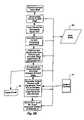
- a method 80 for tracking IC devices through an assembly step 82 in an IC manufacturing process in accordance with the inventionincludes a step 84 of receiving IC devices from multiple, mixed lots 86 .
- the assembly step 82may encompass processing by a single machine, part of a machine, many machines operating in series or parallel, or any combination thereof.
- the step 84 of receiving IC devices from multiple, mixed lots 86is without regard to the lots from which the IC devices come, and thus allows a more efficient use of processing equipment than traditional lot-based procedures.
- the inventionis described as being implemented in a single assembly step 82 for ease of understanding, the invention more typically is implemented in a series of assembly steps.
- a data store 88Before or after the IC devices progress through the assembly step 82 , their lead frame ID codes are read and stored in a data store 88 .
- data related to the assembly step 82is generated for each IC device. Such data may include, for example, the processing equipment used, the operating personnel present, the set-up, and the time and date of processing for the assembly step 82 .
- the set-up for the assembly step 82may include, for example, a standard set-up or a set-up in accordance with a Special Work Request (SWR) or a “hot” lot.
- SWRSpecial Work Request
- the processed IC devicesare output from the assembly step 82 to mixed output lots 90 . It should be understood that, in some cases, the processed IC devices must be cleared from assembly equipment before other IC devices can be processed, and in other cases, such as in serial-feed machines, processed IC devices are being output from the assembly step 82 while other IC devices are advancing through the assembly step 82 and still other IC devices are being received by the assembly step 82 . Any of these cases fall within the scope of the invention.
- the inventive method 80avoids the need for lot-based manufacturing altogether.
- the input and output lots 86 and 90may then be mixed without regard to lots, and the processing of IC devices through the assembly step 82 may proceed in a substantially continuous fashion, thus dramatically improving the utilization of processing equipment.
- the inventive methodis more reliable than conventional tracking procedures (i.e., it eliminates the need for lot travelers).
Landscapes
- Engineering & Computer Science (AREA)
- General Physics & Mathematics (AREA)
- Physics & Mathematics (AREA)
- Microelectronics & Electronic Packaging (AREA)
- Manufacturing & Machinery (AREA)
- Computer Hardware Design (AREA)
- Condensed Matter Physics & Semiconductors (AREA)
- Power Engineering (AREA)
- Automation & Control Theory (AREA)
- General Engineering & Computer Science (AREA)
- Quality & Reliability (AREA)
- General Factory Administration (AREA)
- Testing Or Measuring Of Semiconductors Or The Like (AREA)
- Semiconductor Integrated Circuits (AREA)
Abstract
Description
Claims (26)
Priority Applications (2)
| Application Number | Priority Date | Filing Date | Title |
|---|---|---|---|
| US10/614,917US7120287B2 (en) | 1998-02-20 | 2003-07-07 | Non-lot based method for assembling integrated circuit devices |
| US11/545,059US20070086644A1 (en) | 1998-02-20 | 2006-10-06 | Non-lot based method for assembling integrated circuit devices |
Applications Claiming Priority (5)
| Application Number | Priority Date | Filing Date | Title |
|---|---|---|---|
| US09/027,144US6049624A (en) | 1998-02-20 | 1998-02-20 | Non-lot based method for assembling integrated circuit devices |
| US09/440,736US6226394B1 (en) | 1998-02-20 | 1999-11-16 | Non-lot based method for assembling integrated circuit devices |
| US09/832,163US6400840B2 (en) | 1998-02-20 | 2001-04-09 | Non-lot based method for assembling integrated circuit devices |
| US10/117,244US6588854B2 (en) | 1998-02-20 | 2002-04-05 | Nonlot based method for assembling integrated circuit devices |
| US10/614,917US7120287B2 (en) | 1998-02-20 | 2003-07-07 | Non-lot based method for assembling integrated circuit devices |
Related Parent Applications (1)
| Application Number | Title | Priority Date | Filing Date |
|---|---|---|---|
| US10/117,244ContinuationUS6588854B2 (en) | 1998-02-20 | 2002-04-05 | Nonlot based method for assembling integrated circuit devices |
Related Child Applications (1)
| Application Number | Title | Priority Date | Filing Date |
|---|---|---|---|
| US11/545,059ContinuationUS20070086644A1 (en) | 1998-02-20 | 2006-10-06 | Non-lot based method for assembling integrated circuit devices |
Publications (2)
| Publication Number | Publication Date |
|---|---|
| US20040005090A1 US20040005090A1 (en) | 2004-01-08 |
| US7120287B2true US7120287B2 (en) | 2006-10-10 |
Family
ID=21835958
Family Applications (6)
| Application Number | Title | Priority Date | Filing Date |
|---|---|---|---|
| US09/027,144Expired - LifetimeUS6049624A (en) | 1998-02-20 | 1998-02-20 | Non-lot based method for assembling integrated circuit devices |
| US09/440,736Expired - LifetimeUS6226394B1 (en) | 1998-02-20 | 1999-11-16 | Non-lot based method for assembling integrated circuit devices |
| US09/832,163Expired - Fee RelatedUS6400840B2 (en) | 1998-02-20 | 2001-04-09 | Non-lot based method for assembling integrated circuit devices |
| US10/117,244Expired - LifetimeUS6588854B2 (en) | 1998-02-20 | 2002-04-05 | Nonlot based method for assembling integrated circuit devices |
| US10/614,917Expired - Fee RelatedUS7120287B2 (en) | 1998-02-20 | 2003-07-07 | Non-lot based method for assembling integrated circuit devices |
| US11/545,059AbandonedUS20070086644A1 (en) | 1998-02-20 | 2006-10-06 | Non-lot based method for assembling integrated circuit devices |
Family Applications Before (4)
| Application Number | Title | Priority Date | Filing Date |
|---|---|---|---|
| US09/027,144Expired - LifetimeUS6049624A (en) | 1998-02-20 | 1998-02-20 | Non-lot based method for assembling integrated circuit devices |
| US09/440,736Expired - LifetimeUS6226394B1 (en) | 1998-02-20 | 1999-11-16 | Non-lot based method for assembling integrated circuit devices |
| US09/832,163Expired - Fee RelatedUS6400840B2 (en) | 1998-02-20 | 2001-04-09 | Non-lot based method for assembling integrated circuit devices |
| US10/117,244Expired - LifetimeUS6588854B2 (en) | 1998-02-20 | 2002-04-05 | Nonlot based method for assembling integrated circuit devices |
Family Applications After (1)
| Application Number | Title | Priority Date | Filing Date |
|---|---|---|---|
| US11/545,059AbandonedUS20070086644A1 (en) | 1998-02-20 | 2006-10-06 | Non-lot based method for assembling integrated circuit devices |
Country Status (6)
| Country | Link |
|---|---|
| US (6) | US6049624A (en) |
| EP (1) | EP1062618A4 (en) |
| JP (1) | JP4008198B2 (en) |
| KR (1) | KR100417751B1 (en) |
| AU (1) | AU2481699A (en) |
| WO (1) | WO1999042945A1 (en) |
Cited By (9)
| Publication number | Priority date | Publication date | Assignee | Title |
|---|---|---|---|---|
| US20020183884A1 (en)* | 1997-03-24 | 2002-12-05 | Jones Mark L. | Method for continuous, non lot-based integrated circuit manufacturing |
| US20050096782A1 (en)* | 2003-10-30 | 2005-05-05 | T-Chun Chen | Automated sorter system and method thereof |
| US20060166383A1 (en)* | 2005-01-22 | 2006-07-27 | Samsung Electronics Co., Ltd. | Semiconductor substrate having reference semiconductor chip and method of assembling semiconductor chip using the same |
| US20070094632A1 (en)* | 1997-02-26 | 2007-04-26 | Beffa Raymond J | Method in an integrated circuit (IC) manufacturing process for identifying and redirecting ICs mis-processed during their manufacture |
| US20080149732A1 (en)* | 2006-12-20 | 2008-06-26 | Hsing-Lun Lo | Lot traceable printed circuit board |
| US7502659B2 (en) | 1997-02-17 | 2009-03-10 | Micron Technology, Inc. | Sorting a group of integrated circuit devices for those devices requiring special testing |
| US7561938B2 (en) | 1997-06-06 | 2009-07-14 | Micron Technology, Inc. | Method for using data regarding manufacturing procedures integrated circuits (ICS) have undergone, such as repairs, to select procedures the ICs will undergo, such as additional repairs |
| US7682847B2 (en) | 1997-01-17 | 2010-03-23 | Micron Technology, Inc. | Method for sorting integrated circuit devices |
| US20100274717A1 (en)* | 2009-04-22 | 2010-10-28 | Shaun Wright | Global Internet Based Method and System For Compiling, Assigning, Registration, and Maintenance of Unique Tags |
Families Citing this family (49)
| Publication number | Priority date | Publication date | Assignee | Title |
|---|---|---|---|---|
| US5927512A (en)* | 1997-01-17 | 1999-07-27 | Micron Technology, Inc. | Method for sorting integrated circuit devices |
| US5907492A (en)* | 1997-06-06 | 1999-05-25 | Micron Technology, Inc. | Method for using data regarding manufacturing procedures integrated circuits (IC's) have undergone, such as repairs, to select procedures the IC's will undergo, such as additional repairs |
| US6049624A (en)* | 1998-02-20 | 2000-04-11 | Micron Technology, Inc. | Non-lot based method for assembling integrated circuit devices |
| US6760472B1 (en)* | 1998-12-14 | 2004-07-06 | Hitachi, Ltd. | Identification method for an article using crystal defects |
| US6200823B1 (en)* | 1999-02-09 | 2001-03-13 | Advanced Micro Devices, Inc. | Method for isolation of optical defect images |
| DE10010948A1 (en)* | 2000-03-06 | 2001-09-27 | Siemens Ag | Electronic device containing permanent information, for identification marking |
| US6483334B1 (en)* | 2000-09-28 | 2002-11-19 | United Microelectronics Corp. | Method for reliability testing of semiconductor IC |
| US6469384B2 (en) | 2001-02-01 | 2002-10-22 | Fairchild Semiconductor Corporation | Unmolded package for a semiconductor device |
| US6901984B1 (en)* | 2001-02-27 | 2005-06-07 | Cypress Semiconductor Corporation | Method and system for controlling the processing of an integrated circuit chip assembly line using a central computer system and a common communication protocol |
| US6931298B1 (en) | 2001-02-27 | 2005-08-16 | Cypress Semiconductor Corporation | Integrated back-end integrated circuit manufacturing assembly |
| MY127433A (en)* | 2001-05-29 | 2006-12-29 | Integrated Device Tech | Die bonding apparatus with automatic die and lead frame image matching system. |
| US6601008B1 (en)* | 2001-08-02 | 2003-07-29 | Lsi Logic Corporation | Parametric device signature |
| US6792365B2 (en)* | 2001-08-10 | 2004-09-14 | Micron Technology, Inc. | Sequential unique marking |
| JP3870780B2 (en)* | 2001-12-21 | 2007-01-24 | ヤマハ株式会社 | Manufacturing method of semiconductor device |
| US7840803B2 (en)* | 2002-04-16 | 2010-11-23 | Massachusetts Institute Of Technology | Authentication of integrated circuits |
| WO2003091290A1 (en)* | 2002-04-23 | 2003-11-06 | Boehringer Ingelheim Pharmaceuticals, Inc. | Method for reduction of residual organic solvent in carbomer |
| US7668702B2 (en)* | 2002-07-19 | 2010-02-23 | Applied Materials, Inc. | Method, system and medium for controlling manufacturing process using adaptive models based on empirical data |
| DE10259049A1 (en)* | 2002-12-17 | 2004-07-15 | Infineon Technologies Ag | Integrated semiconductor module |
| JP2004253637A (en)* | 2003-02-20 | 2004-09-09 | Hitachi High-Technologies Corp | Semiconductor device and semiconductor manufacturing management system |
| WO2005052705A1 (en)* | 2003-11-28 | 2005-06-09 | Matsushita Electric Industrial Co., Ltd. | Circuit substrate manufacturing method and system, substrate used for the same, and circuit substrate using the same |
| US7415317B2 (en)* | 2004-02-25 | 2008-08-19 | Micron Technology, Inc. | Method and system for correlating and combining production and non-production data for analysis |
| US7395130B2 (en)* | 2004-02-27 | 2008-07-01 | Micron Technology, Inc. | Method and system for aggregating and combining manufacturing data for analysis |
| US7105377B1 (en)* | 2004-04-13 | 2006-09-12 | Cypress Semiconductor Corporation | Method and system for universal packaging in conjunction with a back-end integrated circuit manufacturing process |
| US7134599B2 (en)* | 2004-06-09 | 2006-11-14 | Inventec Appliances Corp. | Circuit board inspection apparatus |
| EP1810326A1 (en)* | 2004-10-15 | 2007-07-25 | Applied Materials, Inc. | Die-level traceability mechanism for semiconductor assembly and test facility |
| US7622313B2 (en)* | 2005-07-29 | 2009-11-24 | Freescale Semiconductor, Inc. | Fabrication of three dimensional integrated circuit employing multiple die panels |
| US20070050075A1 (en)* | 2005-08-26 | 2007-03-01 | Electro Scientific Industries, Inc. | Automatic wafer tracking process and apparatus for carrying out the process |
| US7684608B2 (en)* | 2006-02-23 | 2010-03-23 | Vistech Corporation | Tape and reel inspection system |
| TW200807425A (en)* | 2006-06-05 | 2008-02-01 | Renesas Tech Corp | Semiconductor device, unique ID of semiconductor device and method for verifying unique ID |
| US7494846B2 (en)* | 2007-03-09 | 2009-02-24 | Taiwan Semiconductor Manufacturing Company, Ltd. | Design techniques for stacking identical memory dies |
| US20090288057A1 (en)* | 2008-05-15 | 2009-11-19 | Texas Instruments Incorporated | System and Method for Ordering the Selection of Integrated Circuit Chips |
| DE102009015496A1 (en)* | 2009-03-30 | 2010-10-07 | Siemens Electronics Assembly Systems Gmbh & Co. Kg | Method for detecting and tracking elements to be loaded |
| JP5315186B2 (en) | 2009-09-18 | 2013-10-16 | ルネサスエレクトロニクス株式会社 | Manufacturing method of semiconductor device |
| US20110156033A1 (en)* | 2009-12-31 | 2011-06-30 | Stmicroelectronics Asia Pacific Pte. Ltd. | Method and system for tracing die at unit level |
| CN102129880B (en)* | 2010-01-14 | 2015-09-30 | 旺宏电子股份有限公司 | 3D Chip Picking for Shared Input Packages |
| US8377747B2 (en)* | 2010-04-21 | 2013-02-19 | Texas Instruments Incorporated | Interleaf for leadframe identification |
| KR101785618B1 (en) | 2012-02-02 | 2017-11-06 | 삼성전자주식회사 | A method for searching the position of multi sim mobile station |
| JP5970948B2 (en)* | 2012-05-11 | 2016-08-17 | 凸版印刷株式会社 | Production management system and production management method |
| JP5968705B2 (en)* | 2012-07-13 | 2016-08-10 | ルネサスエレクトロニクス株式会社 | Manufacturing method of semiconductor device |
| JP2013157626A (en)* | 2013-04-11 | 2013-08-15 | Renesas Electronics Corp | Semiconductor device manufacturing method |
| JP2015114814A (en)* | 2013-12-11 | 2015-06-22 | 株式会社デンソー | Product history management method of semiconductor device |
| WO2016035117A1 (en)* | 2014-09-01 | 2016-03-10 | 三菱電機株式会社 | Semiconductor device, semiconductor chip, and method for managing information on semiconductor chip properties |
| US10714427B2 (en) | 2016-09-08 | 2020-07-14 | Asml Netherlands B.V. | Secure chips with serial numbers |
| NL2019504B1 (en)* | 2016-09-08 | 2018-07-02 | Mapper Lithography Ip Bv | Secure chips with serial numbers |
| US10418324B2 (en) | 2016-10-27 | 2019-09-17 | Asml Netherlands B.V. | Fabricating unique chips using a charged particle multi-beamlet lithography system |
| CN110249408B (en)* | 2016-12-23 | 2023-05-12 | Asml荷兰有限公司 | Security chip with serial number |
| KR102653937B1 (en)* | 2018-07-17 | 2024-04-02 | 삼성전자주식회사 | Test method for semiconductor devices and test system for semiconductor devices |
| US11666100B2 (en) | 2020-01-13 | 2023-06-06 | Altria Client Services Llc | Nicotine electronic vaping device |
| US11771139B2 (en) | 2020-01-13 | 2023-10-03 | Altria Client Services Llc | Non-nicotine electronic vaping device with memory module |
Citations (125)
| Publication number | Priority date | Publication date | Assignee | Title |
|---|---|---|---|---|
| US4027246A (en) | 1976-03-26 | 1977-05-31 | International Business Machines Corporation | Automated integrated circuit manufacturing system |
| US4032949A (en) | 1975-05-15 | 1977-06-28 | Raytheon Company | Integrated circuit fusing technique |
| US4150331A (en) | 1977-07-29 | 1979-04-17 | Burroughs Corporation | Signature encoding for integrated circuits |
| JPS5850728A (en) | 1981-09-19 | 1983-03-25 | Mitsubishi Electric Corp | Manufacture of semiconductor device |
| JPS5852814A (en) | 1981-09-24 | 1983-03-29 | Nec Corp | Semiconductor integrated circuit |
| JPS5860529A (en) | 1981-10-06 | 1983-04-11 | Mitsubishi Electric Corp | Identifying method for semiconductor chip |
| US4454413A (en) | 1982-02-19 | 1984-06-12 | Precision Monolithics, Inc. | Apparatus for tracking integrated circuit devices |
| US4455495A (en) | 1979-10-01 | 1984-06-19 | Hitachi, Ltd. | Programmable semiconductor integrated circuitry including a programming semiconductor element |
| US4510673A (en) | 1983-06-23 | 1985-04-16 | International Business Machines Corporation | Laser written chip identification method |
| US4534014A (en) | 1983-06-20 | 1985-08-06 | Ames Oliver C | Mechanically programmable read only memory |
| JPS61120433A (en) | 1984-11-16 | 1986-06-07 | Toshiba Corp | die bonding equipment |
| US4667403A (en) | 1984-05-16 | 1987-05-26 | Siemens Aktiengesellschaft | Method for manufacturing electronic card modules |
| US4871963A (en) | 1986-07-22 | 1989-10-03 | Sgs Microelettronica S.P.A. | Method and apparatus for testing EPROM type semiconductor devices during burn-in |
| JPH02164017A (en) | 1988-12-19 | 1990-06-25 | Tokyo Electron Ltd | Semiconductor manufacturing apparatus |
| US4954453A (en) | 1989-02-24 | 1990-09-04 | At&T Bell Laboratories | Method of producing an article comprising a multichip assembly |
| US4958373A (en) | 1987-03-31 | 1990-09-18 | Kabushiki Kaisha Toshiba | Defect-recognition processing apparatus |
| JPH02246312A (en) | 1989-03-20 | 1990-10-02 | Fujitsu Ltd | How to identify the chip |
| US4967381A (en) | 1985-04-30 | 1990-10-30 | Prometrix Corporation | Process control interface system for managing measurement data |
| US4985988A (en) | 1989-11-03 | 1991-01-22 | Motorola, Inc. | Method for assembling, testing, and packaging integrated circuits |
| US5003251A (en) | 1989-09-12 | 1991-03-26 | Grumman Aerospace Corporation | Bar code reader for printed circuit board |
| US5043657A (en) | 1990-07-13 | 1991-08-27 | Analog Devices, Incorporated | Marking techniques for identifying integrated circuit parts at the time of testing |
| JPH0480949A (en) | 1990-07-23 | 1992-03-13 | Hitachi Ltd | Lead frame |
| US5103166A (en) | 1990-05-23 | 1992-04-07 | Samsung Electronics Co., Ltd. | Semiconductor integrated circuit chip having an identification circuit therein |
| US5105362A (en) | 1987-04-03 | 1992-04-14 | Mitsubishi Denki Kabushiki Kaisha | Method for producing semiconductor devices |
| US5110754A (en) | 1991-10-04 | 1992-05-05 | Micron Technology, Inc. | Method of making a DRAM capacitor for use as an programmable antifuse for redundancy repair/options on a DRAM |
| US5118369A (en) | 1990-08-23 | 1992-06-02 | Colorcode Unlimited Corporation | Microlabelling system and process for making microlabels |
| JPH04318911A (en) | 1991-04-17 | 1992-11-10 | Matsushita Electric Ind Co Ltd | How to manage processing processes on a multi-product production line |
| US5175774A (en) | 1990-10-16 | 1992-12-29 | Micron Technology, Inc. | Semiconductor wafer marking for identification during processing |
| JPH0513529A (en) | 1991-07-05 | 1993-01-22 | Nec Kyushu Ltd | Semiconductor integrated circuit |
| US5197650A (en) | 1990-09-18 | 1993-03-30 | Sharp Kabushiki Kaisha | Die bonding apparatus |
| JPH05121573A (en) | 1991-10-28 | 1993-05-18 | Sharp Corp | Marking method |
| US5217834A (en) | 1990-08-14 | 1993-06-08 | Kabushiki Kaisha Toshiba | Methods of forming and inspecting semiconductor device patterns |
| US5219765A (en) | 1990-09-12 | 1993-06-15 | Hitachi, Ltd. | Method for manufacturing a semiconductor device including wafer aging, probe inspection, and feeding back the results of the inspection to the device fabrication process |
| US5226118A (en) | 1991-01-29 | 1993-07-06 | Prometrix Corporation | Data analysis system and method for industrial process control systems |
| US5235550A (en) | 1991-05-16 | 1993-08-10 | Micron Technology, Inc. | Method for maintaining optimum biasing voltage and standby current levels in a DRAM array having repaired row-to-column shorts |
| US5253208A (en) | 1991-04-12 | 1993-10-12 | Hyundai Electronics Industries Co., Ltd. | Identification circuit for indicating redundant row or column substitution |
| JPH0574909B2 (en) | 1984-12-27 | 1993-10-19 | Toyota Motor Co Ltd | |
| US5256562A (en) | 1990-12-31 | 1993-10-26 | Kopin Corporation | Method for manufacturing a semiconductor device using a circuit transfer film |
| US5256578A (en) | 1991-12-23 | 1993-10-26 | Motorola, Inc. | Integral semiconductor wafer map recording |
| JPH05315207A (en) | 1992-05-08 | 1993-11-26 | Nec Corp | Semiconductor device |
| US5271796A (en) | 1991-03-27 | 1993-12-21 | Kabushiki Kaisha Toshiba | Method and apparatus for detecting defect on semiconductor substrate surface |
| JPH0613443A (en) | 1992-06-26 | 1994-01-21 | Toshiba Seiki Kk | Manufacture of semiconductor device |
| US5289113A (en) | 1989-08-01 | 1994-02-22 | Analog Devices, Inc. | PROM for integrated circuit identification and testing |
| US5294812A (en) | 1990-09-14 | 1994-03-15 | Kabushiki Kaisha Toshiba | Semiconductor device having identification region for carrying out failure analysis |
| US5296402A (en) | 1992-07-07 | 1994-03-22 | Hyundai Electronics Industries Co., Ltd. | Method for manufacturing a DRAM having a second effective capacitor area |
| US5301143A (en) | 1992-12-31 | 1994-04-05 | Micron Semiconductor, Inc. | Method for identifying a semiconductor die using an IC with programmable links |
| US5326709A (en) | 1991-12-19 | 1994-07-05 | Samsung Electronics Co., Ltd. | Wafer testing process of a semiconductor device comprising a redundancy circuit |
| US5345110A (en) | 1993-04-13 | 1994-09-06 | Micron Semiconductor, Inc. | Low-power fuse detect and latch circuit |
| US5347463A (en) | 1990-07-03 | 1994-09-13 | Honda Giken Kogyo Kabushiki Kaisha | System and method for line production management |
| JPH06267809A (en) | 1993-03-17 | 1994-09-22 | Hitachi Ltd | Multiple-chamber apparatus having wafer-id reading function |
| US5350715A (en) | 1991-11-12 | 1994-09-27 | Samsung Electronics Co., Ltd. | Chip identification scheme |
| US5352945A (en) | 1993-03-18 | 1994-10-04 | Micron Semiconductor, Inc. | Voltage compensating delay element |
| US5355320A (en) | 1992-03-06 | 1994-10-11 | Vlsi Technology, Inc. | System for controlling an integrated product process for semiconductor wafers and packages |
| US5360747A (en) | 1993-06-10 | 1994-11-01 | Xilinx, Inc. | Method of reducing dice testing with on-chip identification |
| JPH06349691A (en) | 1993-06-03 | 1994-12-22 | Hitachi Ltd | Semiconductor device and device and method for manufacturing it |
| JPH0766091A (en) | 1993-08-25 | 1995-03-10 | Sony Corp | Wafer, identification information reading method, method and apparatus for manufacturing integrated circuit |
| US5399531A (en) | 1990-12-17 | 1995-03-21 | United Micrpelectronics Corporation | Single semiconductor wafer transfer method and plural processing station manufacturing system |
| US5420796A (en) | 1993-12-23 | 1995-05-30 | Vlsi Technology, Inc. | Method of inspecting planarity of wafer surface after etchback step in integrated circuit fabrication |
| JPH0750233B2 (en) | 1987-03-17 | 1995-05-31 | 富士通株式会社 | How to install optical cable with connector on the same floor |
| US5424652A (en) | 1992-06-10 | 1995-06-13 | Micron Technology, Inc. | Method and apparatus for testing an unpackaged semiconductor die |
| US5428311A (en) | 1993-06-30 | 1995-06-27 | Sgs-Thomson Microelectronics, Inc. | Fuse circuitry to control the propagation delay of an IC |
| US5440240A (en) | 1991-06-04 | 1995-08-08 | Micron Technology, Inc. | Z-axis interconnect for discrete die burn-in for nonpackaged die |
| US5440493A (en) | 1993-04-15 | 1995-08-08 | Nec Corporation | Lot transporting system between stations having different manufacturing equipment |
| US5442561A (en) | 1992-05-12 | 1995-08-15 | Nippon Telegraph And Telephone Corporation | Production management system and its application method |
| US5448488A (en) | 1993-02-26 | 1995-09-05 | Sony Corporation | Computer-controlled individual chip management system for processing wafers |
| US5450326A (en) | 1994-07-06 | 1995-09-12 | Harris Corporation | Graphical display discriminant factor indicator for anomaly identification in semiconductor manufacture batch process |
| US5467304A (en) | 1993-11-17 | 1995-11-14 | Nec Corporation | Semiconductor integrated circuit |
| US5477493A (en) | 1993-10-04 | 1995-12-19 | Nec Corporation | Semiconductor device having a boundary scan test circuit |
| US5483175A (en) | 1992-04-10 | 1996-01-09 | Micron Technology, Inc. | Method for circuits connection for wafer level burning and testing of individual dies on semiconductor wafer |
| US5495417A (en) | 1990-08-14 | 1996-02-27 | Kabushiki Kaisha Toshiba | System for automatically producing different semiconductor products in different quantities through a plurality of processes along a production line |
| US5504369A (en) | 1993-07-23 | 1996-04-02 | Motorola Inc. | Apparatus for performing wafer level testing of integrated circuit dice |
| US5511005A (en) | 1994-02-16 | 1996-04-23 | Ade Corporation | Wafer handling and processing system |
| US5516028A (en) | 1993-11-10 | 1996-05-14 | Rasp; Richard A. | Process and system for temperature control and in-line testing of electronic, electromechanical and mechanical modules |
| JPH08162380A (en) | 1994-12-05 | 1996-06-21 | Nissan Motor Co Ltd | Method of production control and quality control of electronic parts |
| US5537325A (en) | 1991-10-29 | 1996-07-16 | Komatsu Electronic Metals Co., Ltd. | Apparatus for and method of manufacturing semiconductor wafer |
| US5538141A (en) | 1994-09-27 | 1996-07-23 | Intel Corporation | Test flow assurance using memory imprinting |
| US5539235A (en) | 1994-02-04 | 1996-07-23 | Advanced Micro Devices, Inc. | Metal programmed transistor array |
| US5563832A (en) | 1993-10-29 | 1996-10-08 | Nec Corporation | Semiconductor memory device having interface units memorizing available memory cell sub-arrays |
| US5568408A (en) | 1993-11-22 | 1996-10-22 | Nec Corporation | Automatic repair data editing system associated with repairing system for semiconductor integrated circuit device |
| US5570293A (en) | 1990-11-29 | 1996-10-29 | Tokyo Seimitsu Co., Ltd. | Method and device for manufacturing a semiconductor chip |
| US5581510A (en) | 1994-06-28 | 1996-12-03 | Mitsubishi Denki Kabushiki Kaisha | Method of testing flash memory |
| US5590069A (en) | 1994-10-17 | 1996-12-31 | Qualcomm Incorporated | Method and apparatus for providing ROM in an integrated circuit having update through single substance layer modification capability |
| US5600171A (en) | 1993-07-15 | 1997-02-04 | Mitsubishi Denki Kabushiki Kaisha | Mask ROM device |
| US5606193A (en) | 1994-10-03 | 1997-02-25 | Sharp Kabushiki Kaisha | DRAM and MROM cells with similar structure |
| US5617366A (en) | 1994-12-13 | 1997-04-01 | Samsung Electronics Co., Ltd. | Method and apparatus for a test control circuit of a semiconductor memory device |
| US5619469A (en) | 1995-05-26 | 1997-04-08 | Lg Semicon Co., Ltd. | Fuse redundancy circuitry for a semiconductor memory device |
| US5625816A (en) | 1994-04-05 | 1997-04-29 | Advanced Micro Devices, Inc. | Method and system for generating product performance history |
| US5642307A (en) | 1992-07-09 | 1997-06-24 | Advanced Micro Devices, Inc. | Die identifier and die indentification method |
| US5654204A (en) | 1994-07-20 | 1997-08-05 | Anderson; James C. | Die sorter |
| US5726074A (en) | 1994-12-08 | 1998-03-10 | Nec Corporation | Method and apparatus for manufacturing semiconductor device |
| JPH10104315A (en) | 1996-09-27 | 1998-04-24 | Nec Corp | Device and method for inspecting semiconductor integrated circuit |
| US5764650A (en) | 1996-08-02 | 1998-06-09 | Micron Technology, Inc. | Intelligent binning for electrically repairable semiconductor chips |
| EP0849675A2 (en) | 1996-12-18 | 1998-06-24 | Texas Instruments Incorporated | Volatile memory chip with non-volatile memory locations for storing quality information |
| US5787190A (en) | 1995-06-07 | 1998-07-28 | Advanced Micro Devices, Inc. | Method and apparatus for pattern recognition of wafer test bins |
| US5787012A (en) | 1995-11-17 | 1998-07-28 | Sun Microsystems, Inc. | Integrated circuit with identification signal writing circuitry distributed on multiple metal layers |
| US5801067A (en) | 1993-10-27 | 1998-09-01 | Ronald Shaw | Method for recording and identifying integrated circuit chips and the like |
| US5801965A (en) | 1993-12-28 | 1998-09-01 | Hitachi, Ltd. | Method and system for manufacturing semiconductor devices, and method and system for inspecting semiconductor devices |
| US5805472A (en) | 1996-02-27 | 1998-09-08 | Kabushiki Kaisha Toshiba | Test handler for semiconductor devices |
| US5828778A (en) | 1995-07-13 | 1998-10-27 | Matsushita Electric Industrial Co., Ltd. | Method and apparatus for analyzing failure of semiconductor wafer |
| US5837558A (en) | 1997-11-04 | 1998-11-17 | Texas Instruments Incorporated | Integrated circuit chip packaging method |
| US5844803A (en) | 1997-02-17 | 1998-12-01 | Micron Technology, Inc. | Method of sorting a group of integrated circuit devices for those devices requiring special testing |
| US5856923A (en) | 1997-03-24 | 1999-01-05 | Micron Technology, Inc. | Method for continuous, non lot-based integrated circuit manufacturing |
| JPH118327A (en) | 1997-06-16 | 1999-01-12 | Sony Corp | Method for providing semiconductor chip identification code and method for managing semiconductor chip |
| US5867505A (en) | 1996-08-07 | 1999-02-02 | Micron Technology, Inc. | Method and apparatus for testing an integrated circuit including the step/means for storing an associated test identifier in association with integrated circuit identifier for each test to be performed on the integrated circuit |
| US5865319A (en) | 1994-12-28 | 1999-02-02 | Advantest Corp. | Automatic test handler system for IC tester |
| US5890807A (en) | 1995-10-28 | 1999-04-06 | Deutsche Itt Industries Gmbh | Method for identifying an apparatus or device utilizing a randomly produced characteristic thereof |
| US5895962A (en) | 1996-06-13 | 1999-04-20 | Micron Technology, Inc. | Structure and a method for storing information in a semiconductor device |
| US5907492A (en) | 1997-06-06 | 1999-05-25 | Micron Technology, Inc. | Method for using data regarding manufacturing procedures integrated circuits (IC's) have undergone, such as repairs, to select procedures the IC's will undergo, such as additional repairs |
| US5915231A (en) | 1997-02-26 | 1999-06-22 | Micron Technology, Inc. | Method in an integrated circuit (IC) manufacturing process for identifying and redirecting IC's mis-processed during their manufacture |
| US5927512A (en) | 1997-01-17 | 1999-07-27 | Micron Technology, Inc. | Method for sorting integrated circuit devices |
| US5963881A (en) | 1995-09-22 | 1999-10-05 | Texas Instruments Incorporated | Method and system for enhancing the identification of causes of variations in the performance of manufactured articles |
| US5976899A (en) | 1996-09-13 | 1999-11-02 | Micron Technology, Inc. | Reduced terminal testing system |
| US5991699A (en) | 1995-05-04 | 1999-11-23 | Kla Instruments Corporation | Detecting groups of defects in semiconductor feature space |
| US6000830A (en) | 1997-04-18 | 1999-12-14 | Tokyo Electron Limited | System for applying recipe of semiconductor manufacturing apparatus |
| US6018686A (en) | 1997-10-31 | 2000-01-25 | Cypress Semiconductor Corp. | Electrically imprinting a semiconductor die with identifying information |
| US6049624A (en) | 1998-02-20 | 2000-04-11 | Micron Technology, Inc. | Non-lot based method for assembling integrated circuit devices |
| US6055463A (en) | 1997-05-20 | 2000-04-25 | Samsung Electronics Co. Ltd. | Control system and method for semiconductor integrated circuit test process |
| US6072574A (en) | 1997-01-30 | 2000-06-06 | Micron Technology, Inc. | Integrated circuit defect review and classification process |
| US6075216A (en) | 1994-06-30 | 2000-06-13 | Advantest Corp. | Device transfer and reinspection method for IC handler |
| US6100486A (en) | 1998-08-13 | 2000-08-08 | Micron Technology, Inc. | Method for sorting integrated circuit devices |
| US6138256A (en) | 1998-03-27 | 2000-10-24 | Micron Technology, Inc. | Intelligent binning for electrically repairable semiconductor chips |
| US6194738B1 (en) | 1996-06-13 | 2001-02-27 | Micron Technology, Inc. | Method and apparatus for storage of test results within an integrated circuit |
| US6265232B1 (en) | 1998-08-21 | 2001-07-24 | Micron Technology, Inc. | Yield based, in-line defect sampling method |
| US6636068B2 (en) | 1998-05-22 | 2003-10-21 | Micron Technology Inc | Device and method for isolating a short-circuited integrated circuit (IC) from other ICs on a semiconductor wafer |
| US6895538B2 (en) | 2000-07-18 | 2005-05-17 | Infineon Technologies Ag | Method for testing a device and a test configuration including a device with a test memory |
Family Cites Families (3)
| Publication number | Priority date | Publication date | Assignee | Title |
|---|---|---|---|---|
| US535295A (en)* | 1895-03-05 | Filter | ||
| JPH0574909A (en)* | 1990-12-17 | 1993-03-26 | Asia Electron Inc | Wafer test method |
| KR100189180B1 (en)* | 1996-05-28 | 1999-06-01 | 오우라 히로시 | Separation type handler system for ic tester |
- 1998
- 1998-02-20USUS09/027,144patent/US6049624A/ennot_activeExpired - Lifetime
- 1999
- 1999-01-29JPJP2000532808Apatent/JP4008198B2/ennot_activeExpired - Fee Related
- 1999-01-29EPEP99904416Apatent/EP1062618A4/ennot_activeWithdrawn
- 1999-01-29WOPCT/US1999/001916patent/WO1999042945A1/enactiveIP Right Grant
- 1999-01-29AUAU24816/99Apatent/AU2481699A/ennot_activeAbandoned
- 1999-01-29KRKR10-2000-7009243Apatent/KR100417751B1/ennot_activeExpired - Fee Related
- 1999-11-16USUS09/440,736patent/US6226394B1/ennot_activeExpired - Lifetime
- 2001
- 2001-04-09USUS09/832,163patent/US6400840B2/ennot_activeExpired - Fee Related
- 2002
- 2002-04-05USUS10/117,244patent/US6588854B2/ennot_activeExpired - Lifetime
- 2003
- 2003-07-07USUS10/614,917patent/US7120287B2/ennot_activeExpired - Fee Related
- 2006
- 2006-10-06USUS11/545,059patent/US20070086644A1/ennot_activeAbandoned
Patent Citations (164)
| Publication number | Priority date | Publication date | Assignee | Title |
|---|---|---|---|---|
| US4032949A (en) | 1975-05-15 | 1977-06-28 | Raytheon Company | Integrated circuit fusing technique |
| US4027246A (en) | 1976-03-26 | 1977-05-31 | International Business Machines Corporation | Automated integrated circuit manufacturing system |
| US4150331A (en) | 1977-07-29 | 1979-04-17 | Burroughs Corporation | Signature encoding for integrated circuits |
| US4455495A (en) | 1979-10-01 | 1984-06-19 | Hitachi, Ltd. | Programmable semiconductor integrated circuitry including a programming semiconductor element |
| JPS5850728A (en) | 1981-09-19 | 1983-03-25 | Mitsubishi Electric Corp | Manufacture of semiconductor device |
| JPS5852814A (en) | 1981-09-24 | 1983-03-29 | Nec Corp | Semiconductor integrated circuit |
| JPS5860529A (en) | 1981-10-06 | 1983-04-11 | Mitsubishi Electric Corp | Identifying method for semiconductor chip |
| US4454413A (en) | 1982-02-19 | 1984-06-12 | Precision Monolithics, Inc. | Apparatus for tracking integrated circuit devices |
| US4534014A (en) | 1983-06-20 | 1985-08-06 | Ames Oliver C | Mechanically programmable read only memory |
| US4510673A (en) | 1983-06-23 | 1985-04-16 | International Business Machines Corporation | Laser written chip identification method |
| US4667403A (en) | 1984-05-16 | 1987-05-26 | Siemens Aktiengesellschaft | Method for manufacturing electronic card modules |
| JPS61120433A (en) | 1984-11-16 | 1986-06-07 | Toshiba Corp | die bonding equipment |
| JPH0574909B2 (en) | 1984-12-27 | 1993-10-19 | Toyota Motor Co Ltd | |
| US4967381A (en) | 1985-04-30 | 1990-10-30 | Prometrix Corporation | Process control interface system for managing measurement data |
| US4871963A (en) | 1986-07-22 | 1989-10-03 | Sgs Microelettronica S.P.A. | Method and apparatus for testing EPROM type semiconductor devices during burn-in |
| JPH0750233B2 (en) | 1987-03-17 | 1995-05-31 | 富士通株式会社 | How to install optical cable with connector on the same floor |
| US4958373A (en) | 1987-03-31 | 1990-09-18 | Kabushiki Kaisha Toshiba | Defect-recognition processing apparatus |
| US5105362A (en) | 1987-04-03 | 1992-04-14 | Mitsubishi Denki Kabushiki Kaisha | Method for producing semiconductor devices |
| JPH02164017A (en) | 1988-12-19 | 1990-06-25 | Tokyo Electron Ltd | Semiconductor manufacturing apparatus |
| US4954453A (en) | 1989-02-24 | 1990-09-04 | At&T Bell Laboratories | Method of producing an article comprising a multichip assembly |
| JPH02246312A (en) | 1989-03-20 | 1990-10-02 | Fujitsu Ltd | How to identify the chip |
| US5289113A (en) | 1989-08-01 | 1994-02-22 | Analog Devices, Inc. | PROM for integrated circuit identification and testing |
| US5003251A (en) | 1989-09-12 | 1991-03-26 | Grumman Aerospace Corporation | Bar code reader for printed circuit board |
| US4985988A (en) | 1989-11-03 | 1991-01-22 | Motorola, Inc. | Method for assembling, testing, and packaging integrated circuits |
| US5103166A (en) | 1990-05-23 | 1992-04-07 | Samsung Electronics Co., Ltd. | Semiconductor integrated circuit chip having an identification circuit therein |
| US5347463A (en) | 1990-07-03 | 1994-09-13 | Honda Giken Kogyo Kabushiki Kaisha | System and method for line production management |
| US5043657A (en) | 1990-07-13 | 1991-08-27 | Analog Devices, Incorporated | Marking techniques for identifying integrated circuit parts at the time of testing |
| JPH0480949A (en) | 1990-07-23 | 1992-03-13 | Hitachi Ltd | Lead frame |
| US5495417A (en) | 1990-08-14 | 1996-02-27 | Kabushiki Kaisha Toshiba | System for automatically producing different semiconductor products in different quantities through a plurality of processes along a production line |
| US5217834A (en) | 1990-08-14 | 1993-06-08 | Kabushiki Kaisha Toshiba | Methods of forming and inspecting semiconductor device patterns |
| US5118369A (en) | 1990-08-23 | 1992-06-02 | Colorcode Unlimited Corporation | Microlabelling system and process for making microlabels |
| US5219765A (en) | 1990-09-12 | 1993-06-15 | Hitachi, Ltd. | Method for manufacturing a semiconductor device including wafer aging, probe inspection, and feeding back the results of the inspection to the device fabrication process |
| US5294812A (en) | 1990-09-14 | 1994-03-15 | Kabushiki Kaisha Toshiba | Semiconductor device having identification region for carrying out failure analysis |
| US5197650A (en) | 1990-09-18 | 1993-03-30 | Sharp Kabushiki Kaisha | Die bonding apparatus |
| US5175774A (en) | 1990-10-16 | 1992-12-29 | Micron Technology, Inc. | Semiconductor wafer marking for identification during processing |
| US5570293A (en) | 1990-11-29 | 1996-10-29 | Tokyo Seimitsu Co., Ltd. | Method and device for manufacturing a semiconductor chip |
| US5399531A (en) | 1990-12-17 | 1995-03-21 | United Micrpelectronics Corporation | Single semiconductor wafer transfer method and plural processing station manufacturing system |
| US5256562A (en) | 1990-12-31 | 1993-10-26 | Kopin Corporation | Method for manufacturing a semiconductor device using a circuit transfer film |
| US5226118A (en) | 1991-01-29 | 1993-07-06 | Prometrix Corporation | Data analysis system and method for industrial process control systems |
| US5271796A (en) | 1991-03-27 | 1993-12-21 | Kabushiki Kaisha Toshiba | Method and apparatus for detecting defect on semiconductor substrate surface |
| US5253208A (en) | 1991-04-12 | 1993-10-12 | Hyundai Electronics Industries Co., Ltd. | Identification circuit for indicating redundant row or column substitution |
| JPH04318911A (en) | 1991-04-17 | 1992-11-10 | Matsushita Electric Ind Co Ltd | How to manage processing processes on a multi-product production line |
| US5235550A (en) | 1991-05-16 | 1993-08-10 | Micron Technology, Inc. | Method for maintaining optimum biasing voltage and standby current levels in a DRAM array having repaired row-to-column shorts |
| US5440240A (en) | 1991-06-04 | 1995-08-08 | Micron Technology, Inc. | Z-axis interconnect for discrete die burn-in for nonpackaged die |
| JPH0513529A (en) | 1991-07-05 | 1993-01-22 | Nec Kyushu Ltd | Semiconductor integrated circuit |
| US5110754A (en) | 1991-10-04 | 1992-05-05 | Micron Technology, Inc. | Method of making a DRAM capacitor for use as an programmable antifuse for redundancy repair/options on a DRAM |
| JPH05121573A (en) | 1991-10-28 | 1993-05-18 | Sharp Corp | Marking method |
| US5537325A (en) | 1991-10-29 | 1996-07-16 | Komatsu Electronic Metals Co., Ltd. | Apparatus for and method of manufacturing semiconductor wafer |
| US5350715A (en) | 1991-11-12 | 1994-09-27 | Samsung Electronics Co., Ltd. | Chip identification scheme |
| US5326709A (en) | 1991-12-19 | 1994-07-05 | Samsung Electronics Co., Ltd. | Wafer testing process of a semiconductor device comprising a redundancy circuit |
| US5256578A (en) | 1991-12-23 | 1993-10-26 | Motorola, Inc. | Integral semiconductor wafer map recording |
| US5355320A (en) | 1992-03-06 | 1994-10-11 | Vlsi Technology, Inc. | System for controlling an integrated product process for semiconductor wafers and packages |
| US5483175A (en) | 1992-04-10 | 1996-01-09 | Micron Technology, Inc. | Method for circuits connection for wafer level burning and testing of individual dies on semiconductor wafer |
| JPH05315207A (en) | 1992-05-08 | 1993-11-26 | Nec Corp | Semiconductor device |
| US5442561A (en) | 1992-05-12 | 1995-08-15 | Nippon Telegraph And Telephone Corporation | Production management system and its application method |
| US5424652A (en) | 1992-06-10 | 1995-06-13 | Micron Technology, Inc. | Method and apparatus for testing an unpackaged semiconductor die |
| JPH0613443A (en) | 1992-06-26 | 1994-01-21 | Toshiba Seiki Kk | Manufacture of semiconductor device |
| US5296402A (en) | 1992-07-07 | 1994-03-22 | Hyundai Electronics Industries Co., Ltd. | Method for manufacturing a DRAM having a second effective capacitor area |
| US5642307A (en) | 1992-07-09 | 1997-06-24 | Advanced Micro Devices, Inc. | Die identifier and die indentification method |
| US5301143A (en) | 1992-12-31 | 1994-04-05 | Micron Semiconductor, Inc. | Method for identifying a semiconductor die using an IC with programmable links |
| US5448488A (en) | 1993-02-26 | 1995-09-05 | Sony Corporation | Computer-controlled individual chip management system for processing wafers |
| JPH06267809A (en) | 1993-03-17 | 1994-09-22 | Hitachi Ltd | Multiple-chamber apparatus having wafer-id reading function |
| US5352945A (en) | 1993-03-18 | 1994-10-04 | Micron Semiconductor, Inc. | Voltage compensating delay element |
| US5345110A (en) | 1993-04-13 | 1994-09-06 | Micron Semiconductor, Inc. | Low-power fuse detect and latch circuit |
| US5440493A (en) | 1993-04-15 | 1995-08-08 | Nec Corporation | Lot transporting system between stations having different manufacturing equipment |
| JPH06349691A (en) | 1993-06-03 | 1994-12-22 | Hitachi Ltd | Semiconductor device and device and method for manufacturing it |
| US5360747A (en) | 1993-06-10 | 1994-11-01 | Xilinx, Inc. | Method of reducing dice testing with on-chip identification |
| US5428311A (en) | 1993-06-30 | 1995-06-27 | Sgs-Thomson Microelectronics, Inc. | Fuse circuitry to control the propagation delay of an IC |
| US5600171A (en) | 1993-07-15 | 1997-02-04 | Mitsubishi Denki Kabushiki Kaisha | Mask ROM device |
| US5504369A (en) | 1993-07-23 | 1996-04-02 | Motorola Inc. | Apparatus for performing wafer level testing of integrated circuit dice |
| JPH0766091A (en) | 1993-08-25 | 1995-03-10 | Sony Corp | Wafer, identification information reading method, method and apparatus for manufacturing integrated circuit |
| US5477493A (en) | 1993-10-04 | 1995-12-19 | Nec Corporation | Semiconductor device having a boundary scan test circuit |
| US5801067A (en) | 1993-10-27 | 1998-09-01 | Ronald Shaw | Method for recording and identifying integrated circuit chips and the like |
| US5563832A (en) | 1993-10-29 | 1996-10-08 | Nec Corporation | Semiconductor memory device having interface units memorizing available memory cell sub-arrays |
| US5516028A (en) | 1993-11-10 | 1996-05-14 | Rasp; Richard A. | Process and system for temperature control and in-line testing of electronic, electromechanical and mechanical modules |
| US5467304A (en) | 1993-11-17 | 1995-11-14 | Nec Corporation | Semiconductor integrated circuit |
| US5568408A (en) | 1993-11-22 | 1996-10-22 | Nec Corporation | Automatic repair data editing system associated with repairing system for semiconductor integrated circuit device |
| US5420796A (en) | 1993-12-23 | 1995-05-30 | Vlsi Technology, Inc. | Method of inspecting planarity of wafer surface after etchback step in integrated circuit fabrication |
| US5801965A (en) | 1993-12-28 | 1998-09-01 | Hitachi, Ltd. | Method and system for manufacturing semiconductor devices, and method and system for inspecting semiconductor devices |
| US5539235A (en) | 1994-02-04 | 1996-07-23 | Advanced Micro Devices, Inc. | Metal programmed transistor array |
| US5511005A (en) | 1994-02-16 | 1996-04-23 | Ade Corporation | Wafer handling and processing system |
| US6148307A (en) | 1994-04-05 | 2000-11-14 | Advanced Micro Devices, Inc. | Method and system for generating product performance history |
| US5889674A (en) | 1994-04-05 | 1999-03-30 | Advanced Micro Devices, Inc. | Method and system for generating product performance history |
| US5625816A (en) | 1994-04-05 | 1997-04-29 | Advanced Micro Devices, Inc. | Method and system for generating product performance history |
| US5581510A (en) | 1994-06-28 | 1996-12-03 | Mitsubishi Denki Kabushiki Kaisha | Method of testing flash memory |
| US6075216A (en) | 1994-06-30 | 2000-06-13 | Advantest Corp. | Device transfer and reinspection method for IC handler |
| US5450326A (en) | 1994-07-06 | 1995-09-12 | Harris Corporation | Graphical display discriminant factor indicator for anomaly identification in semiconductor manufacture batch process |
| US5654204A (en) | 1994-07-20 | 1997-08-05 | Anderson; James C. | Die sorter |
| US5603412A (en) | 1994-09-27 | 1997-02-18 | Intel Corporation | Apparatus and semiconductor component for assuring test flow compliance |
| US5538141A (en) | 1994-09-27 | 1996-07-23 | Intel Corporation | Test flow assurance using memory imprinting |
| US5606193A (en) | 1994-10-03 | 1997-02-25 | Sharp Kabushiki Kaisha | DRAM and MROM cells with similar structure |
| US5590069A (en) | 1994-10-17 | 1996-12-31 | Qualcomm Incorporated | Method and apparatus for providing ROM in an integrated circuit having update through single substance layer modification capability |
| JPH08162380A (en) | 1994-12-05 | 1996-06-21 | Nissan Motor Co Ltd | Method of production control and quality control of electronic parts |
| US5726074A (en) | 1994-12-08 | 1998-03-10 | Nec Corporation | Method and apparatus for manufacturing semiconductor device |
| US5617366A (en) | 1994-12-13 | 1997-04-01 | Samsung Electronics Co., Ltd. | Method and apparatus for a test control circuit of a semiconductor memory device |
| US5865319A (en) | 1994-12-28 | 1999-02-02 | Advantest Corp. | Automatic test handler system for IC tester |
| US5991699A (en) | 1995-05-04 | 1999-11-23 | Kla Instruments Corporation | Detecting groups of defects in semiconductor feature space |
| US5619469A (en) | 1995-05-26 | 1997-04-08 | Lg Semicon Co., Ltd. | Fuse redundancy circuitry for a semiconductor memory device |
| US5787190A (en) | 1995-06-07 | 1998-07-28 | Advanced Micro Devices, Inc. | Method and apparatus for pattern recognition of wafer test bins |
| US5828778A (en) | 1995-07-13 | 1998-10-27 | Matsushita Electric Industrial Co., Ltd. | Method and apparatus for analyzing failure of semiconductor wafer |
| US5963881A (en) | 1995-09-22 | 1999-10-05 | Texas Instruments Incorporated | Method and system for enhancing the identification of causes of variations in the performance of manufactured articles |
| US5890807A (en) | 1995-10-28 | 1999-04-06 | Deutsche Itt Industries Gmbh | Method for identifying an apparatus or device utilizing a randomly produced characteristic thereof |
| US5787012A (en) | 1995-11-17 | 1998-07-28 | Sun Microsystems, Inc. | Integrated circuit with identification signal writing circuitry distributed on multiple metal layers |
| US5805472A (en) | 1996-02-27 | 1998-09-08 | Kabushiki Kaisha Toshiba | Test handler for semiconductor devices |
| US6365421B2 (en) | 1996-06-13 | 2002-04-02 | Micron Technology, Inc. | Method and apparatus for storage of test results within an integrated circuit |
| US6194738B1 (en) | 1996-06-13 | 2001-02-27 | Micron Technology, Inc. | Method and apparatus for storage of test results within an integrated circuit |
| US6190972B1 (en) | 1996-06-13 | 2001-02-20 | Micron Technology, Inc. | Method for storing information in a semiconductor device |
| US5895962A (en) | 1996-06-13 | 1999-04-20 | Micron Technology, Inc. | Structure and a method for storing information in a semiconductor device |
| US6219810B1 (en) | 1996-08-02 | 2001-04-17 | Micron Technology, Inc. | Intelligent binning for electrically repairable semiconductor chips |
| US5764650A (en) | 1996-08-02 | 1998-06-09 | Micron Technology, Inc. | Intelligent binning for electrically repairable semiconductor chips |
| US5867505A (en) | 1996-08-07 | 1999-02-02 | Micron Technology, Inc. | Method and apparatus for testing an integrated circuit including the step/means for storing an associated test identifier in association with integrated circuit identifier for each test to be performed on the integrated circuit |
| US6534785B1 (en) | 1996-09-13 | 2003-03-18 | Micron Technology, Inc. | Reduced terminal testing system |
| US6292009B1 (en) | 1996-09-13 | 2001-09-18 | Micron Technology, Inc. | Reduced terminal testing system |
| US5976899A (en) | 1996-09-13 | 1999-11-02 | Micron Technology, Inc. | Reduced terminal testing system |
| US5994915A (en) | 1996-09-13 | 1999-11-30 | Micron Technology, Inc. | Reduced terminal testing system |
| US6424168B1 (en) | 1996-09-13 | 2002-07-23 | Micron Technology, Inc. | Reduced terminal testing system |
| JPH10104315A (en) | 1996-09-27 | 1998-04-24 | Nec Corp | Device and method for inspecting semiconductor integrated circuit |
| EP0849675A2 (en) | 1996-12-18 | 1998-06-24 | Texas Instruments Incorporated | Volatile memory chip with non-volatile memory locations for storing quality information |
| US6130442A (en) | 1996-12-18 | 2000-10-10 | Texas Instruments Incorporated | Memory chip containing a non-volatile memory register for permanently storing information about the quality of the device and test method therefor |
| US6365860B1 (en) | 1997-01-17 | 2002-04-02 | Micron Technology, Inc. | Method for sorting integrated circuit devices |
| US5927512A (en) | 1997-01-17 | 1999-07-27 | Micron Technology, Inc. | Method for sorting integrated circuit devices |
| US6437271B1 (en) | 1997-01-17 | 2002-08-20 | Micron Technology, Inc. | Method for sorting integrated circuit devices |
| US6373011B1 (en) | 1997-01-17 | 2002-04-16 | Micron Technology, Inc. | Method for sorting integrated circuit devices |
| US6365861B1 (en) | 1997-01-17 | 2002-04-02 | Micron Technology, Inc. | Method for sorting integrated circuit devices |
| US6350959B1 (en) | 1997-01-17 | 2002-02-26 | Micron Technology, Inc. | Method for sorting integrated circuit devices |
| US6307171B1 (en) | 1997-01-17 | 2001-10-23 | Micron Technology, Inc. | Method for sorting integrated circuit devices |
| US6703573B2 (en) | 1997-01-17 | 2004-03-09 | Micron Technology, Inc. | Method for sorting integrated circuit devices |
| US6504123B2 (en) | 1997-01-17 | 2003-01-07 | Micron Technology, Inc. | Process for sorting integrated circuit devices |
| US6147316A (en) | 1997-01-17 | 2000-11-14 | Micron Technology, Inc. | Method for sorting integrated circuit devices |
| US6654114B2 (en) | 1997-01-30 | 2003-11-25 | Micron Technology, Inc. | Integrated circuit defect review and classification process |
| US6259520B1 (en) | 1997-01-30 | 2001-07-10 | Micron Technology, Inc. | Integrated circuit defect review and classification process |
| US6373566B2 (en) | 1997-01-30 | 2002-04-16 | Micron Technology, Inc. | Integrated circuit defect review and classification process |
| US6072574A (en) | 1997-01-30 | 2000-06-06 | Micron Technology, Inc. | Integrated circuit defect review and classification process |
| US6441897B1 (en) | 1997-01-30 | 2002-08-27 | Micron Technology, Inc. | Integrated circuit defect review and classification process |
| US6122563A (en) | 1997-02-17 | 2000-09-19 | Micron Technology, Inc. | Method of sorting a group of integrated circuit devices for those devices requiring special testing |
| US6788993B2 (en) | 1997-02-17 | 2004-09-07 | Micron Technology, Inc. | Sorting a group of integrated circuit devices for those devices requiring special testing |
| US5844803A (en) | 1997-02-17 | 1998-12-01 | Micron Technology, Inc. | Method of sorting a group of integrated circuit devices for those devices requiring special testing |
| US6529793B1 (en) | 1997-02-17 | 2003-03-04 | Micron Technology, Inc. | Method of sorting a group of integrated circuit devices for those devices requiring special testing |
| US6594611B2 (en) | 1997-02-26 | 2003-07-15 | Micron Technology, Inc. | Method in an integrated circuit (IC) manufacturing process for identifying and redirecting IC's mis-processed during their manufacture |
| US5915231A (en) | 1997-02-26 | 1999-06-22 | Micron Technology, Inc. | Method in an integrated circuit (IC) manufacturing process for identifying and redirecting IC's mis-processed during their manufacture |
| US6363329B2 (en) | 1997-02-26 | 2002-03-26 | Micron Technology, Inc. | Method in an integrated circuit (IC) manufacturing process for identifying and redirecting IC's mis-processed during their manufacture |
| US6944567B2 (en) | 1997-02-26 | 2005-09-13 | Micron Technology, Inc. | Method in an integrated circuit (IC) manufacturing process for identifying and redirecting ICs mis-processed during their manufacture |
| US6067507A (en) | 1997-02-26 | 2000-05-23 | Micron Technology, Inc. | Method in an integrated circuit (IC) manufacturing process for identifying and redirecting IC's mis-processd during their manufacture |
| US6208947B1 (en) | 1997-02-26 | 2001-03-27 | Micron Technology, Inc. | Method in an integrated circuit (IC) manufacturing process for identifying and redirecting IC's mis-processed during their manufacture |
| US6427092B1 (en) | 1997-03-24 | 2002-07-30 | Micron Technology, Inc. | Method for continuous, non lot-based integrated circuit manufacturing |
| US5856923A (en) | 1997-03-24 | 1999-01-05 | Micron Technology, Inc. | Method for continuous, non lot-based integrated circuit manufacturing |
| US6000830A (en) | 1997-04-18 | 1999-12-14 | Tokyo Electron Limited | System for applying recipe of semiconductor manufacturing apparatus |
| US6055463A (en) | 1997-05-20 | 2000-04-25 | Samsung Electronics Co. Ltd. | Control system and method for semiconductor integrated circuit test process |
| US6363295B1 (en) | 1997-06-06 | 2002-03-26 | Micron Technology, Inc. | Method for using data regarding manufacturing procedures integrated circuits (IC's) have undergone, such as repairs, to select procedures the IC's will undergo, such as additional repairs |
| US5907492A (en) | 1997-06-06 | 1999-05-25 | Micron Technology, Inc. | Method for using data regarding manufacturing procedures integrated circuits (IC's) have undergone, such as repairs, to select procedures the IC's will undergo, such as additional repairs |
| US6553276B2 (en) | 1997-06-06 | 2003-04-22 | Micron Technology, Inc. | Method of using data regarding manufacturing procedures integrated circuits (IC's) have undergone, such as repairs, to select procedures the IC's will undergo, such as additional repairs |
| JPH118327A (en) | 1997-06-16 | 1999-01-12 | Sony Corp | Method for providing semiconductor chip identification code and method for managing semiconductor chip |
| US6018686A (en) | 1997-10-31 | 2000-01-25 | Cypress Semiconductor Corp. | Electrically imprinting a semiconductor die with identifying information |
| US5837558A (en) | 1997-11-04 | 1998-11-17 | Texas Instruments Incorporated | Integrated circuit chip packaging method |
| US6400840B2 (en) | 1998-02-20 | 2002-06-04 | Micron Technology, Inc. | Non-lot based method for assembling integrated circuit devices |
| US6588854B2 (en) | 1998-02-20 | 2003-07-08 | Micron Technology, Inc. | Nonlot based method for assembling integrated circuit devices |
| US6226394B1 (en) | 1998-02-20 | 2001-05-01 | Micron Tecnology, Inc. | Non-lot based method for assembling integrated circuit devices |
| US6049624A (en) | 1998-02-20 | 2000-04-11 | Micron Technology, Inc. | Non-lot based method for assembling integrated circuit devices |
| US6138256A (en) | 1998-03-27 | 2000-10-24 | Micron Technology, Inc. | Intelligent binning for electrically repairable semiconductor chips |
| US6636068B2 (en) | 1998-05-22 | 2003-10-21 | Micron Technology Inc | Device and method for isolating a short-circuited integrated circuit (IC) from other ICs on a semiconductor wafer |
| US6100486A (en) | 1998-08-13 | 2000-08-08 | Micron Technology, Inc. | Method for sorting integrated circuit devices |
| US6265232B1 (en) | 1998-08-21 | 2001-07-24 | Micron Technology, Inc. | Yield based, in-line defect sampling method |
| US6613590B2 (en) | 1998-08-21 | 2003-09-02 | Micron Technology, Inc. | Yield based, in-line defect sampling method |
| US6895538B2 (en) | 2000-07-18 | 2005-05-17 | Infineon Technologies Ag | Method for testing a device and a test configuration including a device with a test memory |
Non-Patent Citations (2)
| Title |
|---|
| English translation of abstract of Japanese Patent No. 5-74909. |
| Fresonke, Dean, In-Fab Identification of Silicon Wafers with Clean, Laser Marked Barcodes, Advanced Semiconductor Manufacturing Conference and Workshop, 1994, IEEE/SEMI, pp. 157-160. |
Cited By (16)
| Publication number | Priority date | Publication date | Assignee | Title |
|---|---|---|---|---|
| US7875821B2 (en) | 1997-01-17 | 2011-01-25 | Micron Technology, Inc. | Method for sorting integrated circuit devices |
| US7682847B2 (en) | 1997-01-17 | 2010-03-23 | Micron Technology, Inc. | Method for sorting integrated circuit devices |
| US7502659B2 (en) | 1997-02-17 | 2009-03-10 | Micron Technology, Inc. | Sorting a group of integrated circuit devices for those devices requiring special testing |
| US20070094632A1 (en)* | 1997-02-26 | 2007-04-26 | Beffa Raymond J | Method in an integrated circuit (IC) manufacturing process for identifying and redirecting ICs mis-processed during their manufacture |
| US7885782B2 (en) | 1997-02-26 | 2011-02-08 | Micron Technology, Inc. | Method in an integrated circuit (IC) manufacturing process for identifying and redirecting ICs mis-processed during their manufacture |
| US8600540B2 (en) | 1997-03-24 | 2013-12-03 | Micron Technology, Inc. | Methods for non-lot-based manufacturing of articles |
| US8315730B2 (en) | 1997-03-24 | 2012-11-20 | Micron Technology, Inc. | Methods for non lot-based integrated circuit manufacturing |
| US20020183884A1 (en)* | 1997-03-24 | 2002-12-05 | Jones Mark L. | Method for continuous, non lot-based integrated circuit manufacturing |
| US7738988B2 (en) | 1997-03-24 | 2010-06-15 | Micron Technology, Inc. | Process and method for continuous, non lot-based integrated circuit manufacturing |
| US7561938B2 (en) | 1997-06-06 | 2009-07-14 | Micron Technology, Inc. | Method for using data regarding manufacturing procedures integrated circuits (ICS) have undergone, such as repairs, to select procedures the ICs will undergo, such as additional repairs |
| US20050096782A1 (en)* | 2003-10-30 | 2005-05-05 | T-Chun Chen | Automated sorter system and method thereof |
| US7618832B2 (en)* | 2005-01-22 | 2009-11-17 | Samsung Electronics Co., Ltd. | Semiconductor substrate having reference semiconductor chip and method of assembling semiconductor chip using the same |
| US20060166383A1 (en)* | 2005-01-22 | 2006-07-27 | Samsung Electronics Co., Ltd. | Semiconductor substrate having reference semiconductor chip and method of assembling semiconductor chip using the same |
| US7576287B2 (en)* | 2006-12-20 | 2009-08-18 | Nan Ya Printed Circuit Board Corporation | Lot traceable printed circuit board |
| US20080149732A1 (en)* | 2006-12-20 | 2008-06-26 | Hsing-Lun Lo | Lot traceable printed circuit board |
| US20100274717A1 (en)* | 2009-04-22 | 2010-10-28 | Shaun Wright | Global Internet Based Method and System For Compiling, Assigning, Registration, and Maintenance of Unique Tags |
Also Published As
| Publication number | Publication date |
|---|---|
| US20010021265A1 (en) | 2001-09-13 |
| US6049624A (en) | 2000-04-11 |
| US20070086644A1 (en) | 2007-04-19 |
| JP4008198B2 (en) | 2007-11-14 |
| EP1062618A4 (en) | 2006-01-25 |
| US6226394B1 (en) | 2001-05-01 |
| KR100417751B1 (en) | 2004-02-11 |
| KR20010034519A (en) | 2001-04-25 |
| JP2003524873A (en) | 2003-08-19 |
| US6400840B2 (en) | 2002-06-04 |
| US20040005090A1 (en) | 2004-01-08 |
| US6588854B2 (en) | 2003-07-08 |
| WO1999042945A1 (en) | 1999-08-26 |
| AU2481699A (en) | 1999-09-06 |
| EP1062618A1 (en) | 2000-12-27 |
| US20020110270A1 (en) | 2002-08-15 |
Similar Documents
| Publication | Publication Date | Title |
|---|---|---|
| US7120287B2 (en) | Non-lot based method for assembling integrated circuit devices | |
| US7738988B2 (en) | Process and method for continuous, non lot-based integrated circuit manufacturing | |
| US6363329B2 (en) | Method in an integrated circuit (IC) manufacturing process for identifying and redirecting IC's mis-processed during their manufacture | |
| US6788993B2 (en) | Sorting a group of integrated circuit devices for those devices requiring special testing | |
| US6363295B1 (en) | Method for using data regarding manufacturing procedures integrated circuits (IC's) have undergone, such as repairs, to select procedures the IC's will undergo, such as additional repairs |
Legal Events
| Date | Code | Title | Description |
|---|---|---|---|
| FEPP | Fee payment procedure | Free format text:PAYOR NUMBER ASSIGNED (ORIGINAL EVENT CODE: ASPN); ENTITY STATUS OF PATENT OWNER: LARGE ENTITY | |
| CC | Certificate of correction | ||
| FPAY | Fee payment | Year of fee payment:4 | |
| FPAY | Fee payment | Year of fee payment:8 | |
| AS | Assignment | Owner name:U.S. BANK NATIONAL ASSOCIATION, AS COLLATERAL AGENT, CALIFORNIA Free format text:SECURITY INTEREST;ASSIGNOR:MICRON TECHNOLOGY, INC.;REEL/FRAME:038669/0001 Effective date:20160426 Owner name:U.S. BANK NATIONAL ASSOCIATION, AS COLLATERAL AGEN Free format text:SECURITY INTEREST;ASSIGNOR:MICRON TECHNOLOGY, INC.;REEL/FRAME:038669/0001 Effective date:20160426 | |
| AS | Assignment | Owner name:MORGAN STANLEY SENIOR FUNDING, INC., AS COLLATERAL AGENT, MARYLAND Free format text:PATENT SECURITY AGREEMENT;ASSIGNOR:MICRON TECHNOLOGY, INC.;REEL/FRAME:038954/0001 Effective date:20160426 Owner name:MORGAN STANLEY SENIOR FUNDING, INC., AS COLLATERAL Free format text:PATENT SECURITY AGREEMENT;ASSIGNOR:MICRON TECHNOLOGY, INC.;REEL/FRAME:038954/0001 Effective date:20160426 | |
| AS | Assignment | Owner name:U.S. BANK NATIONAL ASSOCIATION, AS COLLATERAL AGENT, CALIFORNIA Free format text:CORRECTIVE ASSIGNMENT TO CORRECT THE REPLACE ERRONEOUSLY FILED PATENT #7358718 WITH THE CORRECT PATENT #7358178 PREVIOUSLY RECORDED ON REEL 038669 FRAME 0001. ASSIGNOR(S) HEREBY CONFIRMS THE SECURITY INTEREST;ASSIGNOR:MICRON TECHNOLOGY, INC.;REEL/FRAME:043079/0001 Effective date:20160426 Owner name:U.S. BANK NATIONAL ASSOCIATION, AS COLLATERAL AGEN Free format text:CORRECTIVE ASSIGNMENT TO CORRECT THE REPLACE ERRONEOUSLY FILED PATENT #7358718 WITH THE CORRECT PATENT #7358178 PREVIOUSLY RECORDED ON REEL 038669 FRAME 0001. ASSIGNOR(S) HEREBY CONFIRMS THE SECURITY INTEREST;ASSIGNOR:MICRON TECHNOLOGY, INC.;REEL/FRAME:043079/0001 Effective date:20160426 | |
| FEPP | Fee payment procedure | Free format text:MAINTENANCE FEE REMINDER MAILED (ORIGINAL EVENT CODE: REM.) | |
| AS | Assignment | Owner name:MICRON TECHNOLOGY, INC., IDAHO Free format text:RELEASE BY SECURED PARTY;ASSIGNOR:U.S. BANK NATIONAL ASSOCIATION, AS COLLATERAL AGENT;REEL/FRAME:047243/0001 Effective date:20180629 | |
| LAPS | Lapse for failure to pay maintenance fees | Free format text:PATENT EXPIRED FOR FAILURE TO PAY MAINTENANCE FEES (ORIGINAL EVENT CODE: EXP.); ENTITY STATUS OF PATENT OWNER: LARGE ENTITY | |
| STCH | Information on status: patent discontinuation | Free format text:PATENT EXPIRED DUE TO NONPAYMENT OF MAINTENANCE FEES UNDER 37 CFR 1.362 | |
| FP | Lapsed due to failure to pay maintenance fee | Effective date:20181010 | |
| AS | Assignment | Owner name:MICRON TECHNOLOGY, INC., IDAHO Free format text:RELEASE BY SECURED PARTY;ASSIGNOR:MORGAN STANLEY SENIOR FUNDING, INC., AS COLLATERAL AGENT;REEL/FRAME:050937/0001 Effective date:20190731 |