US7120047B2 - Device selection circuitry constructed with nanotube technology - Google Patents
Device selection circuitry constructed with nanotube technologyDownload PDFInfo
- Publication number
- US7120047B2 US7120047B2US10/693,241US69324103AUS7120047B2US 7120047 B2US7120047 B2US 7120047B2US 69324103 AUS69324103 AUS 69324103AUS 7120047 B2US7120047 B2US 7120047B2
- Authority
- US
- United States
- Prior art keywords
- nanotube
- layer
- devices
- memory
- nanotubes
- Prior art date
- Legal status (The legal status is an assumption and is not a legal conclusion. Google has not performed a legal analysis and makes no representation as to the accuracy of the status listed.)
- Expired - Lifetime, expires
Links
Images


Classifications
- G—PHYSICS
- G11—INFORMATION STORAGE
- G11C—STATIC STORES
- G11C23/00—Digital stores characterised by movement of mechanical parts to effect storage, e.g. using balls; Storage elements therefor
- B—PERFORMING OPERATIONS; TRANSPORTING
- B82—NANOTECHNOLOGY
- B82Y—SPECIFIC USES OR APPLICATIONS OF NANOSTRUCTURES; MEASUREMENT OR ANALYSIS OF NANOSTRUCTURES; MANUFACTURE OR TREATMENT OF NANOSTRUCTURES
- B82Y10/00—Nanotechnology for information processing, storage or transmission, e.g. quantum computing or single electron logic
- G—PHYSICS
- G11—INFORMATION STORAGE
- G11C—STATIC STORES
- G11C13/00—Digital stores characterised by the use of storage elements not covered by groups G11C11/00, G11C23/00, or G11C25/00
- G11C13/02—Digital stores characterised by the use of storage elements not covered by groups G11C11/00, G11C23/00, or G11C25/00 using elements whose operation depends upon chemical change
- G11C13/025—Digital stores characterised by the use of storage elements not covered by groups G11C11/00, G11C23/00, or G11C25/00 using elements whose operation depends upon chemical change using fullerenes, e.g. C60, or nanotubes, e.g. carbon or silicon nanotubes
- H—ELECTRICITY
- H01—ELECTRIC ELEMENTS
- H01H—ELECTRIC SWITCHES; RELAYS; SELECTORS; EMERGENCY PROTECTIVE DEVICES
- H01H1/00—Contacts
- H01H1/0094—Switches making use of nanoelectromechanical systems [NEMS]
- H—ELECTRICITY
- H10—SEMICONDUCTOR DEVICES; ELECTRIC SOLID-STATE DEVICES NOT OTHERWISE PROVIDED FOR
- H10B—ELECTRONIC MEMORY DEVICES
- H10B99/00—Subject matter not provided for in other groups of this subclass
- H10B99/10—Memory cells having a cross-point geometry
- G—PHYSICS
- G11—INFORMATION STORAGE
- G11C—STATIC STORES
- G11C2213/00—Indexing scheme relating to G11C13/00 for features not covered by this group
- G11C2213/70—Resistive array aspects
- G11C2213/77—Array wherein the memory element being directly connected to the bit lines and word lines without any access device being used
- G—PHYSICS
- G11—INFORMATION STORAGE
- G11C—STATIC STORES
- G11C2213/00—Indexing scheme relating to G11C13/00 for features not covered by this group
- G11C2213/70—Resistive array aspects
- G11C2213/81—Array wherein the array conductors, e.g. word lines, bit lines, are made of nanowires
- H—ELECTRICITY
- H10—SEMICONDUCTOR DEVICES; ELECTRIC SOLID-STATE DEVICES NOT OTHERWISE PROVIDED FOR
- H10D—INORGANIC ELECTRIC SEMICONDUCTOR DEVICES
- H10D86/00—Integrated devices formed in or on insulating or conducting substrates, e.g. formed in silicon-on-insulator [SOI] substrates or on stainless steel or glass substrates
- H10D86/201—Integrated devices formed in or on insulating or conducting substrates, e.g. formed in silicon-on-insulator [SOI] substrates or on stainless steel or glass substrates the substrates comprising an insulating layer on a semiconductor body, e.g. SOI
- Y—GENERAL TAGGING OF NEW TECHNOLOGICAL DEVELOPMENTS; GENERAL TAGGING OF CROSS-SECTIONAL TECHNOLOGIES SPANNING OVER SEVERAL SECTIONS OF THE IPC; TECHNICAL SUBJECTS COVERED BY FORMER USPC CROSS-REFERENCE ART COLLECTIONS [XRACs] AND DIGESTS
- Y10—TECHNICAL SUBJECTS COVERED BY FORMER USPC
- Y10S—TECHNICAL SUBJECTS COVERED BY FORMER USPC CROSS-REFERENCE ART COLLECTIONS [XRACs] AND DIGESTS
- Y10S977/00—Nanotechnology
- Y10S977/70—Nanostructure
- Y10S977/734—Fullerenes, i.e. graphene-based structures, such as nanohorns, nanococoons, nanoscrolls or fullerene-like structures, e.g. WS2 or MoS2 chalcogenide nanotubes, planar C3N4, etc.
- Y10S977/742—Carbon nanotubes, CNTs
- Y—GENERAL TAGGING OF NEW TECHNOLOGICAL DEVELOPMENTS; GENERAL TAGGING OF CROSS-SECTIONAL TECHNOLOGIES SPANNING OVER SEVERAL SECTIONS OF THE IPC; TECHNICAL SUBJECTS COVERED BY FORMER USPC CROSS-REFERENCE ART COLLECTIONS [XRACs] AND DIGESTS
- Y10—TECHNICAL SUBJECTS COVERED BY FORMER USPC
- Y10S—TECHNICAL SUBJECTS COVERED BY FORMER USPC CROSS-REFERENCE ART COLLECTIONS [XRACs] AND DIGESTS
- Y10S977/00—Nanotechnology
- Y10S977/70—Nanostructure
- Y10S977/762—Nanowire or quantum wire, i.e. axially elongated structure having two dimensions of 100 nm or less
- Y10S977/765—Nanowire or quantum wire, i.e. axially elongated structure having two dimensions of 100 nm or less with specified cross-sectional profile, e.g. belt-shaped
- Y—GENERAL TAGGING OF NEW TECHNOLOGICAL DEVELOPMENTS; GENERAL TAGGING OF CROSS-SECTIONAL TECHNOLOGIES SPANNING OVER SEVERAL SECTIONS OF THE IPC; TECHNICAL SUBJECTS COVERED BY FORMER USPC CROSS-REFERENCE ART COLLECTIONS [XRACs] AND DIGESTS
- Y10—TECHNICAL SUBJECTS COVERED BY FORMER USPC
- Y10S—TECHNICAL SUBJECTS COVERED BY FORMER USPC CROSS-REFERENCE ART COLLECTIONS [XRACs] AND DIGESTS
- Y10S977/00—Nanotechnology
- Y10S977/902—Specified use of nanostructure
- Y10S977/932—Specified use of nanostructure for electronic or optoelectronic application
- Y10S977/943—Information storage or retrieval using nanostructure
Definitions
- Electromechanical Memory Array Using Nanotube Ribbons and Method for Making Same(U.S. patent application Ser. No. 09/915,093).
- This inventionrelates in general to nonvolatile memory devices for use as memory storage in an electronic device and in particular to nonvolatile memory arrays that use electromechanical elements as the individual memory cells.
- ROMRead Only Memory
- PROMProgrammable Read only Memory
- EPROMElectrically Programmable Memory
- EEPROMElectrically Erasable Programmable Read Only Memory
- DRAMDynamic Random Access Memory
- SRAMStatic Random Access Memory
- ROMis relatively low cost but cannot be rewritten.
- PROMcan be electrically programmed but with only a single write cycle.
- EPROMhas read cycles that are fast relative to ROM and PROM read cycles, but has relatively long erase times and reliability only over a few iterative read/write cycles.
- EEPROM(or “Flash”) is inexpensive, and has low power consumption but has long write cycles (ms) and low relative speed in comparison to DRAM or SRAM. Flash also has a finite number of read/write cycles leading to low long-term reliability.
- ROM, PROM, EPROM and EEPROMare all non-volatile, meaning that if power to the memory is interrupted the memory will retain the information stored in the memory cells.
- DRAMstores charge on transistor gates that act as capacitors but must be electrically refreshed every few milliseconds complicating system design by requiring separate circuitry to “refresh” the memory contents before the capacitors discharge.
- SRAMdoes not need to be refreshed and is fast relative to DRAM, but has lower density and is more expensive relative to DRAM. Both SRAM and DRAM are volatile, meaning that if power to the memory is interrupted the memory will lose the information stored in the memory cells.
- MRAMmagnetic RAM
- FRAMferromagnetic RAM
- MRAMutilizes the orientation of magnetization or a ferromagnetic region to generate a nonvolatile memory cell.
- MRAMutilizes a magnetoresisitive memory element involving the anisotropic magnetoresistance or giant magnetoresistance of ferromagnetic materials yielding nonvolatility. Both of these types of memory cells have relatively high resistance and low-density.
- a different memory cell based upon magnetic tunnel junctionshas also been examined but has not led to large-scale commercialized MRAM devices.
- FRAMuses a circuit architecture similar to DRAM but which uses a thin film ferroelectric capacitor. This capacitor is purported to retain its electrical polarization after an externally applied electric field is removed yielding a nonvolatile memory.
- FRAMsuffers from a large memory cell size, and it is difficult to manufacture as a large-scale integrated component. See U.S. Pat. Nos. 4,853,893; 4,888,630; 5,198,994
- phase change memoryAnother technology having non-volatile memory is phase change memory.
- This technologystores information via a structural phase change in thin-film alloys incorporating elements such as selenium or tellurium. These alloys are purported to remain stable in both crystalline and amorphous states allowing the formation of a bistable switch. While the nonvolatility condition is met, this technology appears to suffer from slow operations, difficulty of manufacture and reliability and has not reached a state of commercialization. See U.S. Pat. Nos. 3,448,302; 4,845,533; 4,876,667; 6,044,008.
- Wire crossbar memoryhas also been proposed. See U.S. Pat. Nos. 6,128,214; 6,159,620; 6,198,655. These memory proposals envision molecules as bistable switches. Two wires (either a metal or semiconducting type) have a layer of molecules or molecule compounds sandwiched in between. Chemical assembly and electrochemical oxidation or reduction are used to generate an “on” or “off” state. This form of memory requires highly specialized wire junctions and may not retain non-volatility owing to the inherent instability found in redox processes.
- nanoscopic wiressuch as single-walled carbon nanotubes
- nanoscopic wiressuch as single-walled carbon nanotubes
- WO 01/03208Nanoscopic Wire-Based Devices, Arrays, and Methods of Their Manufacture
- Thomas Rueckes et al.“Carbon Nanotube-Based Nonvolatile Random Access Memory for Molecular Computing,” Science, vol. 289, pp. 94–97, 7 Jul., 2000.
- these devicesare called nanotube wire crossbar memories (NTWCMs).
- NSWCMsnanotube wire crossbar memories
- individual single-walled nanotube wires suspended over other wiresdefine memory cells. Electrical signals are written to one or both wires to cause them to physically attract or repel relative to one another.
- Each physical statecorresponds to an electrical state.
- Repelled wiresare an open circuit junction. Attracted wires are a closed state forming a rectified junction. When electrical power is removed from the junction, the wires retain their physical (and thus electrical) state thereby forming a non-volatile memory cell.
- NTWCM proposals to daterely on directed growth or chemical self-assembly techniques to grow the individual nanotubes needed for the memory cells. These techniques are now believed to be difficult to employ at commercial scales using modern technology. Moreover, they may contain inherent limitations such as the length of the nanotubes that may be grown reliably using these techniques, and it may difficult to control the statistical variance of geometries of nanotube wires so grown.
- the inventionprovides a memory system having electromechanical memory cells.
- a decoder circuitselects at least one of the memory cells of an array of such cells.
- Each cell in the arrayis a crossbar junction at least one element of which is a nanotube or a nanotube ribbon.
- the decoder circuitis constructed of crossbar junctions at least one element of each junction being a nanotube or a nanotube ribbon.
- FIG. 1illustrates a nanotube belt crossbar memory device according to certain embodiments of the invention
- FIGS. 2A–Billustrate two states of a memory cell according to certain embodiments of the invention
- FIG. 3illustrates acts of making memory devices according to certain embodiments of the invention
- FIGS. 4–11illustrate several forms of creating an intermediate structure used to make memory devices according to certain embodiments of the invention.
- FIG. 12illustrates the non-woven nanotube fabric, or matted nanotube layer, used to make certain embodiments of the invention
- FIG. 13illustrates the matted nanotube layer in relation to hidden, underlying traces of certain embodiments of the invention
- FIG. 14illustrates addressing logic of certain embodiments of the invention
- FIG. 15illustrates a hybrid technology embodiment of the invention in which the memory core uses nanotube technology
- FIG. 16illustrates a hybrid technology embodiment of the invention in which the memory core and addressing lines use nanotube ribbon technology.
- Preferred embodiments of the inventionprovide new electromechanical memory arrays and methods for making same.
- electromechanical memory cellsare created that operate anaologously to the NTWCM devices disclosed in WO 01/03208, which is hereby incorporated by reference in its entirety.
- preferred embodiments of the inventionreplace the suspended nanoscopic wires used in the NTWCM devices with new ribbons made from a matted layer of nanotubes or a non-woven fabric of nanotubes.
- These new devicesare referred to herein as nanotube ribbon crossbar memories (NTRCMs).
- NRCMsnanotube ribbon crossbar memories
- the new nanotube belt structuresare believed to be easier to build at the desired levels of integration and scale (in number of devices made) and the geometries are more easily controlled.
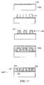
- FIG. 1illustrates an exemplary electromechanical memory array 100 constructed according to principles of preferred embodiments of the invention.
- the arrayhas a plurality of non volatile memory cells 103 which can be in an “on” state 105 or “off” state 106 .
- the actual number of such cellsis immaterial to understanding the invention but the technology may support devices having information storage capacities equivalent to or larger than modern non-volatile circuit devices.
- Each memory cell 103includes a nanotube ribbon 101 suspended by one or more supports 102 over electrical traces or wires, e.g., 104 .
- Each crossing of a ribbon 101 and a wire, e.g., 104forms a crossbar junction and defines a memory cell.
- each cellmay be read or written by applying currents and or voltages to electrodes 112 which are in electrical communication with ribbons 101 or through electrodes (not shown) in communication with traces or wires 104 .
- the supports 102are made from a layer 108 of silicon nitride (Si 3 N 4 ). Below layer 108 is a gate oxide layer 109 separating the n-doped silicon traces 104 from an underlying silicon wafer 110 .
- junction 106illustrates the cell in a first physical and electrical state in which the nanotube ribbon 101 is separated from corresponding trace 104 .
- Junction 105illustrates the cell in a second physical and electrical state in which the nanotube ribbon 101 is deflected toward corresponding trace 104 .
- the junctionIn the first state, the junction is an open circuit, which may be sensed as such on either the ribbon 101 or trace 104 when so addressed.
- the junctionIn the second state, the junction is a rectified junction (e.g., Schottky or PN), which may be sensed as such on either the tube 101 or trace 104 when so addressed.
- PNrectified junction
- the nanotube ribbon 101may be held in position at the supports by friction.
- the ribbonmay be held by other means, such as by anchoring the ribbons to the supports using any of a variety of techniques.
- This frictioncan be increased through the use of chemical interactions including covalent bonding through the use of carbon compounds such as pyrenes or other chemically reactive species.
- Evaporated or spin-coated materialsuch as metals, semiconductors or insulators especially silicon, titanium, silicon oxide or polyimide could also be added to increase the pinning strength.
- the nanotube ribbons or individual nanotubescan also be pinned through the use wafer bonding to the surface. See R. J.
- a nanotube ribbon 101has a width of about 180 nm and is pinned to a support 102 preferably fabricated of silicon nitride.
- the local area of trace 104 under ribbon 101forms an n-doped silicon electrode and is positioned close to the supports 102 and preferably is no wider than the belt, e.g., 180 nm.
- the relative separation 208 from the top of the support 102 to the deflected position where the belt 101 attaches to electrode 206should be approximately 5–50 nm.
- the magnitude of the separation 208is designed to be compatible with electromechanical switching capabilities of the memory device.
- the 5–50 nm separationis preferred for certain embodiments utilizing ribbons 101 made from carbon nanotubes, but other separations may be preferable for other materials. This magnitude arises from the interplay between strain energy and adhesion energy of the deflected nanotubes. These feature sizes are suggested in view of modem manufacturing techniques. Other embodiments may be made with much smaller (or larger) sizes to reflect the manufacturing equipment's capabilities.
- the nanotube ribbon 101 of certain embodimentsis formed from a non-woven fabric of entangled or matted nanotubes (more below).
- the switching parameters of the ribbonresemble those of individual nanotubes.
- the predicted switching times and voltages of the ribbonshould approximate the same times and voltages of nanotubes.
- preferred embodiments of the present inventionutilize fabrication techniques involving thin films and lithography. This method of fabrication lends itself to generation over large surfaces especially wafers of at least six inches.
- the ribbonsshould exhibit improved fault tolerances over individual nanotubes, by providing redundancy of conduction pathways contained with the ribbons. (If an individual nanotube breaks other tubes within the rib provide conductive paths, whereas if a sole nanotube were used the cell would be faulty.) Moreover, the resistances of the ribbons should be significantly lower than that for an individual nanotubes, thus, decreasing its impedance, since the ribbons may be made to have larger cross-sectional areas than individual nanotubes.
- FIG. 3illustrates a method of making certain embodiments of NTRCM devices 100 .
- a first intermediate structure 302is created or provided.
- the structure 302includes a silicon substrate 110 having an insulating layer 109 (such as silicon dioxide) and a silicon nitride layer (Si 3 N 4 ) 108 that defines a plurality of supports 102 .
- the supports 102are formed by rows of patterned silicon nitride, though many other arrangements are possible, such as a plurality of columns.
- Conductive traces 104extend between supports 102 .
- the traces 104are shown as essentially contacting the supports 102 , but other arrangements are possible as are other geometries; for example, spaces may exist between trace 104 and support 102 and trace 104 may be fashioned as a wire or may have non-rectangular transverse, cross-sections, including triangular or trapezoidal.
- Sacrificial layers 304are disposed above the traces 104 so as to define one planar surface 306 with the upper surface of the supports 102 . This planar surface, as will be explained below, facilitates growth of a matted nanotube layer of certain embodiments.
- the upper surface 306receives a catalyst 308 .
- a catalyst metal 308containing iron (Fe), molybdenum (Mo), cobalt or other metals, is applied by spin-coating or other application techniques to create a second intermediate structure 310 .
- a matted layer 312 of nanotubesis then grown into a non-woven fabric of single-walled carbon nanotubes (SWNTs) to form a third intermediate structure 314 .
- the second intermediate structure 310may be placed into an oven and heated to a high temperature (for example, about 800–1200° C.) while gases containing a carbon source, hydrogen and inert gas, such as argon or nitrogen, are flowed over the upper surface.
- gases containing a carbon source, hydrogen and inert gas, such as argon or nitrogenare flowed over the upper surface.
- This environmentfacilitates the generation or growth of the matted layer or film 312 of single-walled carbon nanotubes.
- the layer 312is primarily one nanotube thick and the various tubes adhere to one another via Van der Waals forces.
- the catalyst 308may be patterned to assist in growing the nanotubes with specific densities either more or less dense as is desired.
- nanotubescan be made to evenly distribute over a given field that is primarily a monolayer of nanotubes. Proper growth requires control of parameters including but not limited to catalyst composition and concentration, functionialization of the underlying surface, spin coating parameters (length and RPM), growth time, temperature and gas concentrations.
- a photoresistmay then be applied to the layer 312 and patterned to define ribbons in the matted layer of nanotubes 312 .
- the ribbon patternscross (for example, perpendicularly) the underlying traces 104 .
- the photoresistis removed to leave ribbons 101 of non-woven nanotube fabric lying on planar surface 306 to form fourth intermediate structure 318 .
- the fourth intermediate structure 318has portions 320 of its underlying sacrificial layer 304 exposed as shown.
- the structure 318is then treated with an acid, such as HF, to remove the sacrificial layer 304 , including the portion under the ribbons 101 , thus forming an array 322 of ribbons 101 suspended over traces 104 and supported by supports 102 .
- an acidsuch as HF
- addressing electrodese.g., 112 shown in FIG. 1 .
- One aspect of the above techniqueis that the various growth, patterning, and etching operations may use conventional techniques, such as lithographic patterning.
- thismay entail feature sizes (e.g., width of ribbon 101 ) of about 180 nm to as low as 130 nm, but the physical characteristics of the components are amenable to even smaller feature sizes if manufacturing capabilities permit.
- FIG. 4shows one way to create the first intermediate structure 302
- a silicon wafer 400is provided with an oxide layer 402 .
- the oxide layeris preferably a few nanometers in thickness but could be as much 1 ⁇ m.
- a silicon nitride (Si 3 N 4 ) layer 404is deposited on top of the oxide surface 402 .
- the silicon nitride layeris preferably at least 30 nm thick.
- the silicon nitride layer 404is then patterned and etched to generate cavities 406 to form support structure 407 .
- the cavity widthmay be about 180 nm wide or perhaps smaller.
- the remaining silicon nitride materialdefines the supports 102 (e.g., as row, or perhaps columns).
- a covering 408 of n-doped siliconis then deposited to fill the cavities 406 .
- the covering 408for exemplary embodiments may be about 1 ⁇ m thick but may be as thin as 30 nm.
- the covering 408is then processed, for example by self-flattening of thick silicon layers or by annealing, to produce a planar surface 306 , discussed above, to form structure 411 .
- RIEreactive ion-etching
- EPDend-point detection
- the structure 411is then oxidized to form and define sacrificial layers 304 of SiO 2 about 10–20 nm deep into planar surface 306 .
- the unconverted, remaining portions of siliconform traces 104 .
- FIG. 5shows another method that may be used to create the NTRCM devices 100 of certain embodiments.
- a support structure 407like that described in connection with FIG. 4 , is provided.
- a layer 514 of n-doped siliconis then added using a CVD process, sputtering or electroplating. Under certain embodiments, layer 514 is added to be about half the height of the Si 3 N 4 supports 102 .
- an annealing stepis performed to yield a planarized surface 306 to form a structure 411 like that described above.
- the annealing stepcauses the silicon of layer 514 to flow into the cavities 406 .
- the structure 411is then oxidized to form and define sacrificial layers 304 of SiO 2 about 10–20 nm deep into planar surface 306 .
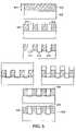
- FIG. 6shows another approach for forming an alternative first intermediate structure 302 ′.
- a silicon substrate 600is covered with a layer 602 of silicon nitride having a height 604 of at least 30 nm.
- the silicon nitride layer 602is then patterned and etched to generate spacings 606 and to defined supports 102 .
- the etching processexposes a portion 608 of the surface of silicon substrate 600 .
- the exposed silicon surface 608is oxidized to generate a silicon dioxide (SiO 2 ) layers 610 having a thickness of a few nm. These layers 610 eventually insulate traces 104 analogously to the way insulating layer 109 did for the above described structures 302 .
- the traces 104may be created in any of a variety of manner.
- FIG. 6illustrates the processing steps of FIGS. 4–5 used to create such traces to illustrate this point.
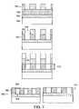
- FIG. 7shows another approach for forming first intermediate structure 302 .
- a silicon substrate 700 having a silicon dioxide layer 702 and a silicon nitride layer 704receives a patterned photoresist layer 706 .
- a photoresist layermay be spin-coated on layer 704 and subsequently exposed and lithographically developed.
- Reactive ion etchingor the like may then be used to etch the Si 3 N 4 layer 704 to form cavities 708 and to define supports 102 .
- n-doped silicon 710may be deposited in the cavities 708 .
- siliconis deposited to a height about equal to the height 712 of the Si 3 N 4 supports 102 .
- the photoresist 706 and silicon 710 on top of the photoresist 706are then stripped away to form an intermediate structure 411 like that described above.
- the structure 411is then oxidized to generate the sacrificial SiO 2 layers 304 .
- FIG. 8shows another approach for forming first intermediate structure 302 .
- a starting structure 800is provided having a lowest silicon layer 802 with a lowest silicon dioxide layer 804 on top of it.
- a second silicon layer 806is on top of layer 804 and a second silicon dioxide layer 808 is on top of the second silicon layer 806 .
- the top silicon dioxide (SiO 2 ) layer 808is patterned by photolithography to create an RIE mask 810 .
- the maskis used to etch the exposed portions 812 of second silicon layer 806 down to the first silicon dioxide layer 804 . This etching creates cavities 814 and defines traces 104 .
- the cavities 814are filled and covered with silicon nitride (Si 3 N 4 ) 816 .
- the Si 3 N 4 covering 816is backetched with RIE to the same height 818 as the remaining portions of the SiO 2 layer 806 covering the n-doped silicon electrodes 104 (which form the sacrificial layer 304 ).
- FIG. 9shows an approach for forming an alternative first intermediate structure 302 ′′.
- a structure like 407shown in FIG. 4 , but not FIG. 9 .
- the Si 3 N 4 supports 102have a height of about 30 nm.
- a thin layer of metal 902is deposited on top of the Si 3 N 4 supports 102 and on top of the exposed portions SiO 2 at the bottom of the cavities 904 as depicted by item 903 .
- Metal 902 and 903form temporary electrodes.
- a layer of n-doped silicon 906may then be deposited or grown by electroplating, covering the electrode 903 until the silicon 906 achieves a height 908 at the top of the support 102 and contacting electrode 902 .
- the growth processmay be controlled by the onset of a current flow between the lower and upper metal electrodes 902 , 3 .
- the exposed metal electrodes 902may then be removed by wet chemical methods or dry chemical methods. This forms an intermediate structure 411 ′ like the structure 411 described above, but with a buried electrode 903 , as an artifact of the silicon growing process.
- the structure 411 ′is then oxidized to form sacrificial layers 304 at the exposed portions of silicon, as described above.
- the layers 304may be grown to a thickness of about 10 nm.
- FIG. 10shows another approach for forming first intermediate structure 302 .
- a silicon substrate 1002 having a layer of silicon dioxide 1004 on top of it and a second layer 1006 of silicon (n-doped) on top of layer 1004is used as a starting material.
- a mask layer 1008is photolithographically patterned on top of layer 1006 .
- exposed portions 1010 of n-doped silicon layer 1006are chemically converted to Si 3 N 4 supports 102 .
- the unconverted portions of layer 1006form traces 104 .
- the mask 1008is removed forming a structure 411 like that described above.
- the exposed portions 1012 of silicon surfaceare then oxidized to form the SiO 2 sacrificial layers 304 .
- FIG. 11shows an approach for forming an alternative first intermediate structure 302 ′′′ Under this approach a silicon substrate 1102 is layered with a thin film 1104 of Si 3 N 4 as a starting structure. On top of the silicon nitride layer 1104 , n-doped silicon is added and lithographically patterned, by RIE, to form traces 104 .
- traces 104are oxidized to form the SiO 2 layer 1106 which acts as an alternative form of sacrificial layer 304 ′.
- the structureis overgrown with Si 3 N 4 1108 and back etched to form a planar surface 306 and to form alternative first intermediate structure 302 ′′′.
- traces 104will be separated from supports 102 .
- Other variations of this techniquemay be employed to create alternative transverse cross-sections of trace 104 .
- the traces 104may be created to have a rounded top, or to have a triangular or trapezoidal cross section.
- the cross sectionmay have other forms, such as a triangle with tapered sides.
- a matted nanotube layer 312is provided over the planar surface 306 of the structure 302 .
- the non-woven fabric layer 312is grown over the structure through the use of a catalyst 308 and through the control of a growth environment.
- Other embodimentsmay provide the matted nanotube layer 312 separately and apply it directly over the structure 302 .
- structure 302 under this approachpreferably includes the sacrificial layer to provide a planar surface to receive the independently grown fabric, the sacrificial layer may not be necessary under such an approach.
- FIG. 12is an approximate depiction of an actual nanotube non-woven fabric.
- nanotubeshave feature sizes as small as 1–2 nm which is below the precision of SEM.
- FIG. 12suggests the fabric's matted nature; not clear from the figure, however, is that the fabric may have small areas of discontinuity with no tubes present.
- Each tubetypically has a diameter 1–2 nm (thus defining a fabric layer about 1–2 nm) but may have lengths of a few microns but may be as long as 200 microns.
- the tubesmay curve and occasionally cross one another. Tubes attach to one another via Van der Waals forces.
- nanotubesgrow substantially unrestrained in the x- and y-axis directions, but are substantially restricted in the z-axis (perpendicular to page of FIG. 12 ) as a consequence of the self-assembly trait.
- Other embodimentsmay supplement the above approach to growing matte 312 with the use of field-oriented or flow-oriented growth techniques. Such supplementation may be used to further tailor growth such that any growth in one planar axis (e.g. the -x-axis) is retarded. This allows for a more even coverage of the desired area with a planar interwoven monolayer coating of nanotubes with a controllable density.
- FIG. 13A plan view of the matted nanotube layer 312 with underlying silicon traces 104 is shown in FIG. 13 .
- the layer 312is patterned and etched to define ribbons 101 of nanotube fabric that cross the supports 102 .
- the sacrificial layeris then removed (e.g., with acid) forming the array 322 described above in connection with FIG. 3 . Because the matted layer of nanotubes 312 form a non-woven fabric that is not a contiguous film, etchants or other chemicals may diffuse between the individual nanotube “fibers” and more easily reach the underlying components, such as the sacrificial layer.
- addressing electrodese.g., 112 shown in FIG. 1 , as outlined above.
- Other embodimentsuse nanotube technology to implement addressing of memory cells instead of using metallized electrodes 112 and addressing lines (not shown).
- nanotubesare used to form NTRCM arrays.
- Certain embodimentsuse nanotube technology, whether in individual wire or belt form, to implement addressing logic to select the memory cell(s) for reading or writing operations.
- This approachfurthers the integration of nanotube technology into system design and may provide beneficial functionality to higher-level system design. For example, under this approach the memory architecture will not only store memory contents in non-volatile manner but will inherently store the last memory address.
- the nanotube-based memory cellshave bistability characterized by a high ratio of resistance between “0” and “1” states. Switching between these states is accomplished by the application of specific voltages across the nanotube belt or wire and the underlying trace, in which at least one of the memory cell elements is a nanotube or a nanotube ribbon. In one approach, a “readout current” is applied and the voltage across this junction is determined with a “sense amplifier.” Reads are non-destructive, meaning that the cell retains its state, and no write-back operations are needed as is done with DRAM.
- FIG. 14depicts a branching binary select system, or decoder, 1400 .
- decoder 1400may be implemented with nanotubes or nanotube ribbon technology.
- the decodermay be constructed on the same circuit component as a nanotube memory cell array, e.g., NTRCM or NTWCM.
- a perpendicular intersection of two lines 1404 and 1406 depicted as a dot 1402indicates a junction of two nanotubes or nanotube ribbons.
- the interactionis analogous to a “pass transistor” found in CMOS and other technology, in which the intersection may be opened or closed.
- Locations such as 1420 where one nanotube or nanotube ribbon may cross another but which are not intended to create a crossbar junctionmay be insulated from one another with a lithographically patterned insulator between the components.
- the decoder illustratedis for a 3-bit binary address carried on addressing lines 1408 .
- the intersections (dots)will be switched to create only one path through which sensing current I may pass to select lines 1418 .
- a “dual rail” representation 1408 of each bit of the binary addressis fashioned externally so that each of the address bits 1410 is presented in true and complementary form.
- line 1406may be the logical true version of address line 1408 a
- line 1407may be the logical complement of address line 1408 a.
- the voltage values of the representation 1408are consistent with that needed to switch a crossbar junction to the “1” or “0” state as described above.
- an address 1408may be used to supply a sense current I to a bit or row of bits in an array, e.g., to nanotubes or nanotube ribbons.
- the same approachmay be used to sense a given trace, for example, selecting specific array column(s) to read sense from in conjunction with selecting a row.
- this approachmay be used for X and/or Y decoding both for reading and for writing operations.
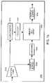
- a core memory cell array 1502is constructed using NTWCM or NTRCM, and that core is surrounded by semiconductor circuits forming X and Y address decoders 1504 and 1506 ; X and Y buffers 1508 and 1510 ; control logic 1512 and output buffers 1514 .
- the circuitry surrounding the NTWCM or NWBCM coremay be used for conventional interfacing functions, including providing read currents and sensing output voltages.
- the X and Y address decoders 1504 and 1506may be substituted with the nanotube wire or belt addressing technique discussed above.
- the corewould include memory cells and addressing logic.
- the hybrid circuit 1500may be formed by using a nanotube core (having either just memory cells or memory cells and addressing logic) and by implementing the surrounding circuitry using a field programmable gate array.
- the core and gate array circuitrymay be contained in a single physical package if desired. Or, they may be packaged separately.
- a hermitically packaged nanotube circuit(having memory or memory and addressing logic) may be combined with a PLD/FPGA/ASIC in which the I/O interfacing logic is contained.
- the resulting compact chipsetprovides access to the benefits of the NT memory for the user of the product, while maximizing the use of “off-the-shelf” technologies, which may be utilized on an as-needed basis by the manufacturer.
- FIG. 16depicts one possible implementation 1600 of the hybrid technology.
- a FPGA chip 1602 containing the buffering and control logic(described above) is connected via conducting traces on a (perhaps multilayer) printed circuit board (PCB) 1604 to a nanotube (NT) chip 1606 containing the memory cells and addressing logic.
- PCBprinted circuit board
- NTnanotube
- the nanotube arraywill be integrated before metallization but after ion implantation and planarization of the CMOS logic devices.
- a second methodinvolves growth of the nanotube arrays before fabrication of the CMOS devices involving ion implementation and high temperature annealing steps. Upon completion of these steps the final metallization of both the nanotube ribbons and the CMOS devices will proceed using standard and widely used protocols.
- Electrodesconsisting of n-doped silicon on top of some metal or semiconductor line can also be envisioned. This will still provide rectifying junctions in the ON state so that no multiple current pathways exist.
- Nanotubescan be functionalized with planar conjugated hydrocarbons such as pyrenes which may then aid in enhancing the internal adhesion between nanotubes within the ribbons.
- Certain of the above aspectsare applicable to individual nanotubes (e.g., using directed growth techniques, etc.) or to nanotube ribbons.
Landscapes
- Engineering & Computer Science (AREA)
- Chemical & Material Sciences (AREA)
- Nanotechnology (AREA)
- Physics & Mathematics (AREA)
- Mathematical Physics (AREA)
- Theoretical Computer Science (AREA)
- Crystallography & Structural Chemistry (AREA)
- Semiconductor Memories (AREA)
Abstract
Description
Claims (10)
Priority Applications (3)
| Application Number | Priority Date | Filing Date | Title |
|---|---|---|---|
| US10/693,241US7120047B2 (en) | 2001-07-25 | 2003-10-24 | Device selection circuitry constructed with nanotube technology |
| US11/546,130US7269052B2 (en) | 2001-07-25 | 2006-10-10 | Device selection circuitry constructed with nanotube technology |
| US11/853,550US8101976B2 (en) | 2001-07-25 | 2007-09-11 | Device selection circuitry constructed with nanotube ribbon technology |
Applications Claiming Priority (2)
| Application Number | Priority Date | Filing Date | Title |
|---|---|---|---|
| US09/915,173US6643165B2 (en) | 2001-07-25 | 2001-07-25 | Electromechanical memory having cell selection circuitry constructed with nanotube technology |
| US10/693,241US7120047B2 (en) | 2001-07-25 | 2003-10-24 | Device selection circuitry constructed with nanotube technology |
Related Parent Applications (1)
| Application Number | Title | Priority Date | Filing Date |
|---|---|---|---|
| US09/915,173ContinuationUS6643165B2 (en) | 2001-07-25 | 2001-07-25 | Electromechanical memory having cell selection circuitry constructed with nanotube technology |
Related Child Applications (1)
| Application Number | Title | Priority Date | Filing Date |
|---|---|---|---|
| US11/546,130ContinuationUS7269052B2 (en) | 2001-07-25 | 2006-10-10 | Device selection circuitry constructed with nanotube technology |
Publications (2)
| Publication Number | Publication Date |
|---|---|
| US20040085805A1 US20040085805A1 (en) | 2004-05-06 |
| US7120047B2true US7120047B2 (en) | 2006-10-10 |
Family
ID=25435352
Family Applications (4)
| Application Number | Title | Priority Date | Filing Date |
|---|---|---|---|
| US09/915,173Expired - LifetimeUS6643165B2 (en) | 2001-07-25 | 2001-07-25 | Electromechanical memory having cell selection circuitry constructed with nanotube technology |
| US10/693,241Expired - LifetimeUS7120047B2 (en) | 2001-07-25 | 2003-10-24 | Device selection circuitry constructed with nanotube technology |
| US11/546,130Expired - LifetimeUS7269052B2 (en) | 2001-07-25 | 2006-10-10 | Device selection circuitry constructed with nanotube technology |
| US11/853,550Expired - Fee RelatedUS8101976B2 (en) | 2001-07-25 | 2007-09-11 | Device selection circuitry constructed with nanotube ribbon technology |
Family Applications Before (1)
| Application Number | Title | Priority Date | Filing Date |
|---|---|---|---|
| US09/915,173Expired - LifetimeUS6643165B2 (en) | 2001-07-25 | 2001-07-25 | Electromechanical memory having cell selection circuitry constructed with nanotube technology |
Family Applications After (2)
| Application Number | Title | Priority Date | Filing Date |
|---|---|---|---|
| US11/546,130Expired - LifetimeUS7269052B2 (en) | 2001-07-25 | 2006-10-10 | Device selection circuitry constructed with nanotube technology |
| US11/853,550Expired - Fee RelatedUS8101976B2 (en) | 2001-07-25 | 2007-09-11 | Device selection circuitry constructed with nanotube ribbon technology |
Country Status (6)
| Country | Link |
|---|---|
| US (4) | US6643165B2 (en) |
| EP (1) | EP1410398A4 (en) |
| AU (1) | AU2002356510A1 (en) |
| CA (1) | CA2454898A1 (en) |
| TW (1) | TWI241687B (en) |
| WO (1) | WO2003023818A2 (en) |
Cited By (17)
| Publication number | Priority date | Publication date | Assignee | Title |
|---|---|---|---|---|
| US20050007002A1 (en)* | 2002-10-29 | 2005-01-13 | President And Fellows Of Harvard College | Carbon nanotube device fabrication |
| US20050218523A1 (en)* | 2004-03-30 | 2005-10-06 | Dubin Valery M | Integrated circuit with metal layer having carbon nanotubes and methods of making same |
| US20060006377A1 (en)* | 2002-10-29 | 2006-01-12 | President And Fellows Of Harvard College | Suspended carbon nanotube field effect transistor |
| US20080152792A1 (en)* | 2006-12-21 | 2008-06-26 | Motorola, Inc. | Method of manufacturing a bistable microelectronic switch stack |
| US20080150672A1 (en)* | 2006-12-21 | 2008-06-26 | Motorola, Inc. | Bistable microelectronic switch stack |
| US20080257859A1 (en)* | 2005-04-06 | 2008-10-23 | President And Fellows Of Harvard College | Molecular characterization with carbon nanotube control |
| US20090074607A1 (en)* | 2007-09-18 | 2009-03-19 | Barrick Gold Corporation | Process for recovering gold and silver from refractory ores |
| US20090136682A1 (en)* | 2007-10-02 | 2009-05-28 | President And Fellows Of Harvard College | Carbon nanotube synthesis for nanopore devices |
| US20090175068A1 (en)* | 2008-01-07 | 2009-07-09 | International Business Machines Corporation | Sram device, and sram device design structure, with adaptable access transistors |
| US20100148183A1 (en)* | 2001-07-25 | 2010-06-17 | Ward Jonathan W | Method of Forming a Carbon Nanotube-Based Contact to Semiconductor |
| US20100288980A1 (en)* | 2007-11-15 | 2010-11-18 | E. I. Du Pont De Nemours And Company | Protection of carbon nanotubes |
| US7897954B2 (en) | 2008-10-10 | 2011-03-01 | Macronix International Co., Ltd. | Dielectric-sandwiched pillar memory device |
| US8262768B2 (en) | 2007-09-17 | 2012-09-11 | Barrick Gold Corporation | Method to improve recovery of gold from double refractory gold ores |
| US8262770B2 (en) | 2007-09-18 | 2012-09-11 | Barrick Gold Corporation | Process for controlling acid in sulfide pressure oxidation processes |
| US8975610B1 (en) | 2013-12-23 | 2015-03-10 | Intermolecular, Inc. | Silicon based selector element |
| US8981327B1 (en) | 2013-12-23 | 2015-03-17 | Intermolecular, Inc. | Carbon-doped silicon based selector element |
| US9012878B1 (en) | 2013-12-23 | 2015-04-21 | Intermolecular, Inc. | MoOx based selector element |
Families Citing this family (260)
| Publication number | Priority date | Publication date | Assignee | Title |
|---|---|---|---|---|
| JP3991602B2 (en)* | 2001-03-02 | 2007-10-17 | 富士ゼロックス株式会社 | Carbon nanotube structure manufacturing method, wiring member manufacturing method, and wiring member |
| US6593666B1 (en) | 2001-06-20 | 2003-07-15 | Ambient Systems, Inc. | Energy conversion systems using nanometer scale assemblies and methods for using same |
| US6835591B2 (en) | 2001-07-25 | 2004-12-28 | Nantero, Inc. | Methods of nanotube films and articles |
| US6643165B2 (en)* | 2001-07-25 | 2003-11-04 | Nantero, Inc. | Electromechanical memory having cell selection circuitry constructed with nanotube technology |
| US6574130B2 (en) | 2001-07-25 | 2003-06-03 | Nantero, Inc. | Hybrid circuit having nanotube electromechanical memory |
| US7566478B2 (en)* | 2001-07-25 | 2009-07-28 | Nantero, Inc. | Methods of making carbon nanotube films, layers, fabrics, ribbons, elements and articles |
| US6706402B2 (en) | 2001-07-25 | 2004-03-16 | Nantero, Inc. | Nanotube films and articles |
| US6919592B2 (en) | 2001-07-25 | 2005-07-19 | Nantero, Inc. | Electromechanical memory array using nanotube ribbons and method for making same |
| US6924538B2 (en) | 2001-07-25 | 2005-08-02 | Nantero, Inc. | Devices having vertically-disposed nanofabric articles and methods of making the same |
| US7259410B2 (en)* | 2001-07-25 | 2007-08-21 | Nantero, Inc. | Devices having horizontally-disposed nanofabric articles and methods of making the same |
| US6672925B2 (en)* | 2001-08-17 | 2004-01-06 | Motorola, Inc. | Vacuum microelectronic device and method |
| US7319057B2 (en)* | 2001-10-30 | 2008-01-15 | Ovonyx, Inc. | Phase change material memory device |
| US6612695B2 (en)* | 2001-11-07 | 2003-09-02 | Michael Waters | Lighted reading glasses |
| CN1311553C (en)* | 2001-12-12 | 2007-04-18 | 松下电器产业株式会社 | Non-volatile memory and its manufacturing method |
| EP1341183B1 (en)* | 2002-02-25 | 2008-12-03 | STMicroelectronics S.r.l. | Optically readable molecular memory obtained using carbon nanotubes, and method for storing information in said molecular memory |
| US7335395B2 (en) | 2002-04-23 | 2008-02-26 | Nantero, Inc. | Methods of using pre-formed nanotubes to make carbon nanotube films, layers, fabrics, ribbons, elements and articles |
| US7304128B2 (en)* | 2002-06-04 | 2007-12-04 | E.I. Du Pont De Nemours And Company | Carbon nanotube binding peptides |
| US6864503B2 (en) | 2002-08-09 | 2005-03-08 | Macronix International Co., Ltd. | Spacer chalcogenide memory method and device |
| US6911373B2 (en)* | 2002-09-20 | 2005-06-28 | Intel Corporation | Ultra-high capacitance device based on nanostructures |
| US7259984B2 (en)* | 2002-11-26 | 2007-08-21 | Cornell Research Foundation, Inc. | Multibit metal nanocrystal memories and fabrication |
| US7858185B2 (en) | 2003-09-08 | 2010-12-28 | Nantero, Inc. | High purity nanotube fabrics and films |
| EP1585845A1 (en)* | 2003-01-13 | 2005-10-19 | Nantero, Inc. | Methods of using thin metal layers to make carbon nanotube films, layers, fabrics, ribbons, elements and articles |
| US7560136B2 (en)* | 2003-01-13 | 2009-07-14 | Nantero, Inc. | Methods of using thin metal layers to make carbon nanotube films, layers, fabrics, ribbons, elements and articles |
| US7294877B2 (en)* | 2003-03-28 | 2007-11-13 | Nantero, Inc. | Nanotube-on-gate FET structures and applications |
| US7113426B2 (en)* | 2003-03-28 | 2006-09-26 | Nantero, Inc. | Non-volatile RAM cell and array using nanotube switch position for information state |
| US7075141B2 (en)* | 2003-03-28 | 2006-07-11 | Nantero, Inc. | Four terminal non-volatile transistor device |
| US6944054B2 (en)* | 2003-03-28 | 2005-09-13 | Nantero, Inc. | NRAM bit selectable two-device nanotube array |
| US6995046B2 (en)* | 2003-04-22 | 2006-02-07 | Nantero, Inc. | Process for making byte erasable devices having elements made with nanotubes |
| US7045421B2 (en)* | 2003-04-22 | 2006-05-16 | Nantero, Inc. | Process for making bit selectable devices having elements made with nanotubes |
| CA2526946A1 (en) | 2003-05-14 | 2005-04-07 | Nantero, Inc. | Sensor platform using a non-horizontally oriented nanotube element |
| US7148579B2 (en)* | 2003-06-02 | 2006-12-12 | Ambient Systems, Inc. | Energy conversion systems utilizing parallel array of automatic switches and generators |
| US7095645B2 (en)* | 2003-06-02 | 2006-08-22 | Ambient Systems, Inc. | Nanoelectromechanical memory cells and data storage devices |
| US7254690B2 (en)* | 2003-06-02 | 2007-08-07 | S. Aqua Semiconductor Llc | Pipelined semiconductor memories and systems |
| US7199498B2 (en)* | 2003-06-02 | 2007-04-03 | Ambient Systems, Inc. | Electrical assemblies using molecular-scale electrically conductive and mechanically flexible beams and methods for application of same |
| US20040238907A1 (en)* | 2003-06-02 | 2004-12-02 | Pinkerton Joseph F. | Nanoelectromechanical transistors and switch systems |
| US7910064B2 (en)* | 2003-06-03 | 2011-03-22 | Nanosys, Inc. | Nanowire-based sensor configurations |
| US7274064B2 (en) | 2003-06-09 | 2007-09-25 | Nanatero, Inc. | Non-volatile electromechanical field effect devices and circuits using same and methods of forming same |
| US7301802B2 (en) | 2003-06-09 | 2007-11-27 | Nantero, Inc. | Circuit arrays having cells with combinations of transistors and nanotube switching elements |
| DE10327530A1 (en) | 2003-06-17 | 2005-01-20 | Electrovac Gesmbh | Device comprising at least one heat source formed by a functional element to be cooled, having at least one heat sink and at least one intermediate layer of a thermal conductive material between the heat source and the heat sink and thermal conductive mass, in particular for use in such a device |
| JP3731589B2 (en)* | 2003-07-18 | 2006-01-05 | ソニー株式会社 | Imaging device and synchronization signal generator |
| US7026432B2 (en) | 2003-08-12 | 2006-04-11 | General Electric Company | Electrically conductive compositions and method of manufacture thereof |
| US7354988B2 (en) | 2003-08-12 | 2008-04-08 | General Electric Company | Electrically conductive compositions and method of manufacture thereof |
| CN1868002B (en)* | 2003-08-13 | 2011-12-14 | 南泰若股份有限公司 | Nanotube-based switching element with multiple controls and circuits made therefrom |
| US7289357B2 (en)* | 2003-08-13 | 2007-10-30 | Nantero, Inc. | Isolation structure for deflectable nanotube elements |
| WO2005017967A2 (en) | 2003-08-13 | 2005-02-24 | Nantero, Inc. | Nanotube device structure and methods of fabrication |
| US7115960B2 (en)* | 2003-08-13 | 2006-10-03 | Nantero, Inc. | Nanotube-based switching elements |
| EP1665278A4 (en)* | 2003-08-13 | 2007-11-07 | Nantero Inc | NANOTUBE SWITCHING ELEMENTS COMPRISING MULTIPLE CONTROLS AND CIRCUITS PRODUCED FROM THESE ELEMENTS |
| US7504051B2 (en)* | 2003-09-08 | 2009-03-17 | Nantero, Inc. | Applicator liquid for use in electronic manufacturing processes |
| US7416993B2 (en)* | 2003-09-08 | 2008-08-26 | Nantero, Inc. | Patterned nanowire articles on a substrate and methods of making the same |
| US7375369B2 (en) | 2003-09-08 | 2008-05-20 | Nantero, Inc. | Spin-coatable liquid for formation of high purity nanotube films |
| US7309727B2 (en) | 2003-09-29 | 2007-12-18 | General Electric Company | Conductive thermoplastic compositions, methods of manufacture and articles derived from such compositions |
| US7528437B2 (en)* | 2004-02-11 | 2009-05-05 | Nantero, Inc. | EEPROMS using carbon nanotubes for cell storage |
| US6969651B1 (en) | 2004-03-26 | 2005-11-29 | Lsi Logic Corporation | Layout design and process to form nanotube cell for nanotube memory applications |
| US20050218397A1 (en)* | 2004-04-06 | 2005-10-06 | Availableip.Com | NANO-electronics for programmable array IC |
| US7312155B2 (en)* | 2004-04-07 | 2007-12-25 | Intel Corporation | Forming self-aligned nano-electrodes |
| US7658869B2 (en)* | 2004-06-03 | 2010-02-09 | Nantero, Inc. | Applicator liquid containing ethyl lactate for preparation of nanotube films |
| US7556746B2 (en)* | 2004-06-03 | 2009-07-07 | Nantero, Inc. | Method of making an applicator liquid for electronics fabrication process |
| US7709880B2 (en)* | 2004-06-09 | 2010-05-04 | Nantero, Inc. | Field effect devices having a gate controlled via a nanotube switching element |
| US7329931B2 (en)* | 2004-06-18 | 2008-02-12 | Nantero, Inc. | Receiver circuit using nanotube-based switches and transistors |
| US7288970B2 (en) | 2004-06-18 | 2007-10-30 | Nantero, Inc. | Integrated nanotube and field effect switching device |
| US7330709B2 (en)* | 2004-06-18 | 2008-02-12 | Nantero, Inc. | Receiver circuit using nanotube-based switches and logic |
| US7167026B2 (en)* | 2004-06-18 | 2007-01-23 | Nantero, Inc. | Tri-state circuit using nanotube switching elements |
| US7161403B2 (en) | 2004-06-18 | 2007-01-09 | Nantero, Inc. | Storage elements using nanotube switching elements |
| US7164744B2 (en)* | 2004-06-18 | 2007-01-16 | Nantero, Inc. | Nanotube-based logic driver circuits |
| US7652342B2 (en)* | 2004-06-18 | 2010-01-26 | Nantero, Inc. | Nanotube-based transfer devices and related circuits |
| CN101061576A (en)* | 2004-06-21 | 2007-10-24 | 3M创新有限公司 | Patterning and aligning semiconductor nanoparticles |
| WO2007024204A2 (en) | 2004-07-19 | 2007-03-01 | Ambient Systems, Inc. | Nanometer-scale electrostatic and electromagnetic motors and generators |
| US6955937B1 (en) | 2004-08-12 | 2005-10-18 | Lsi Logic Corporation | Carbon nanotube memory cell for integrated circuit structure with removable side spacers to permit access to memory cell and process for forming such memory cell |
| TWI399864B (en) | 2004-09-16 | 2013-06-21 | Nantero Inc | Light emitters using nanotubes and methods of making same |
| WO2006132658A2 (en)* | 2004-09-21 | 2006-12-14 | Nantero, Inc. | Resistive elements using carbon nanotubes |
| WO2006137876A2 (en) | 2004-09-22 | 2006-12-28 | Nantero, Inc. | Random access memory including nanotube switching elements |
| US20100147657A1 (en)* | 2004-11-02 | 2010-06-17 | Nantero, Inc. | Nanotube esd protective devices and corresponding nonvolatile and volatile nanotube switches |
| CA2586120A1 (en)* | 2004-11-02 | 2006-12-28 | Nantero, Inc. | Nanotube esd protective devices and corresponding nonvolatile and volatile nanotube switches |
| US20060092695A1 (en)* | 2004-11-02 | 2006-05-04 | Wing Malcolm J | Hybrid memory array with single cycle access |
| US7472576B1 (en) | 2004-11-17 | 2009-01-06 | State Of Oregon Acting By And Through The State Board Of Higher Education On Behalf Of Portland State University | Nanometrology device standards for scanning probe microscopes and processes for their fabrication and use |
| US7608503B2 (en)* | 2004-11-22 | 2009-10-27 | Macronix International Co., Ltd. | Side wall active pin memory and manufacturing method |
| US20090124776A1 (en)* | 2004-11-30 | 2009-05-14 | Hideyuki Takai | Cycloaliphatic epoxy (meth)acrylates, preparation processes thereof, and copolymers |
| EP1825038B1 (en)* | 2004-12-16 | 2012-09-12 | Nantero, Inc. | Aqueous carbon nanotube applicator liquids and methods for producing applicator liquids thereof |
| US8362525B2 (en) | 2005-01-14 | 2013-01-29 | Nantero Inc. | Field effect device having a channel of nanofabric and methods of making same |
| US7598544B2 (en)* | 2005-01-14 | 2009-10-06 | Nanotero, Inc. | Hybrid carbon nanotude FET(CNFET)-FET static RAM (SRAM) and method of making same |
| US7462656B2 (en) | 2005-02-15 | 2008-12-09 | Sabic Innovative Plastics Ip B.V. | Electrically conductive compositions and method of manufacture thereof |
| US9390790B2 (en) | 2005-04-05 | 2016-07-12 | Nantero Inc. | Carbon based nonvolatile cross point memory incorporating carbon based diode select devices and MOSFET select devices for memory and logic applications |
| US9287356B2 (en)* | 2005-05-09 | 2016-03-15 | Nantero Inc. | Nonvolatile nanotube diodes and nonvolatile nanotube blocks and systems using same and methods of making same |
| US9196615B2 (en)* | 2005-05-09 | 2015-11-24 | Nantero Inc. | Nonvolatile nanotube diodes and nonvolatile nanotube blocks and systems using same and methods of making same |
| US7479654B2 (en) | 2005-05-09 | 2009-01-20 | Nantero, Inc. | Memory arrays using nanotube articles with reprogrammable resistance |
| US8013363B2 (en)* | 2005-05-09 | 2011-09-06 | Nantero, Inc. | Nonvolatile nanotube diodes and nonvolatile nanotube blocks and systems using same and methods of making same |
| US7835170B2 (en) | 2005-05-09 | 2010-11-16 | Nantero, Inc. | Memory elements and cross point switches and arrays of same using nonvolatile nanotube blocks |
| US7782650B2 (en)* | 2005-05-09 | 2010-08-24 | Nantero, Inc. | Nonvolatile nanotube diodes and nonvolatile nanotube blocks and systems using same and methods of making same |
| TWI324773B (en) | 2005-05-09 | 2010-05-11 | Nantero Inc | Non-volatile shadow latch using a nanotube switch |
| US8513768B2 (en) | 2005-05-09 | 2013-08-20 | Nantero Inc. | Nonvolatile nanotube diodes and nonvolatile nanotube blocks and systems using same and methods of making same |
| US9911743B2 (en)* | 2005-05-09 | 2018-03-06 | Nantero, Inc. | Nonvolatile nanotube diodes and nonvolatile nanotube blocks and systems using same and methods of making same |
| US7781862B2 (en) | 2005-05-09 | 2010-08-24 | Nantero, Inc. | Two-terminal nanotube devices and systems and methods of making same |
| US7394687B2 (en)* | 2005-05-09 | 2008-07-01 | Nantero, Inc. | Non-volatile-shadow latch using a nanotube switch |
| US8183665B2 (en)* | 2005-11-15 | 2012-05-22 | Nantero Inc. | Nonvolatile nanotube diodes and nonvolatile nanotube blocks and systems using same and methods of making same |
| US8217490B2 (en) | 2005-05-09 | 2012-07-10 | Nantero Inc. | Nonvolatile nanotube diodes and nonvolatile nanotube blocks and systems using same and methods of making same |
| US7598127B2 (en)* | 2005-05-12 | 2009-10-06 | Nantero, Inc. | Nanotube fuse structure |
| US7575693B2 (en)* | 2005-05-23 | 2009-08-18 | Nantero, Inc. | Method of aligning nanotubes and wires with an etched feature |
| US7928521B1 (en) | 2005-05-31 | 2011-04-19 | Nantero, Inc. | Non-tensioned carbon nanotube switch design and process for making same |
| US7402770B2 (en) | 2005-06-10 | 2008-07-22 | Lsi Logic Corporation | Nano structure electrode design |
| US7321130B2 (en) | 2005-06-17 | 2008-01-22 | Macronix International Co., Ltd. | Thin film fuse phase change RAM and manufacturing method |
| US7696503B2 (en) | 2005-06-17 | 2010-04-13 | Macronix International Co., Ltd. | Multi-level memory cell having phase change element and asymmetrical thermal boundary |
| US7238994B2 (en)* | 2005-06-17 | 2007-07-03 | Macronix International Co., Ltd. | Thin film plate phase change ram circuit and manufacturing method |
| JP5019192B2 (en)* | 2005-06-24 | 2012-09-05 | 株式会社東芝 | Semiconductor device |
| US7349236B2 (en)* | 2005-06-24 | 2008-03-25 | Xerox Corporation | Electromechanical memory cell with torsional movement |
| US7538040B2 (en) | 2005-06-30 | 2009-05-26 | Nantero, Inc. | Techniques for precision pattern transfer of carbon nanotubes from photo mask to wafers |
| US7495952B2 (en)* | 2005-07-13 | 2009-02-24 | Cornell Research Foundation, Inc. | Relay-connected semiconductor transistors |
| US7612424B1 (en) | 2005-07-22 | 2009-11-03 | Northwestern University | Nanoelectromechanical bistable cantilever device |
| ATE518131T1 (en)* | 2005-09-06 | 2011-08-15 | Nantero Inc | NANOTUBE-BASED SENSOR SYSTEM AND METHOD FOR USE THEREOF |
| AU2006347609A1 (en) | 2005-09-06 | 2008-05-08 | Nantero, Inc. | Carbon nanotubes for the selective transfer of heat from electronics |
| US7446044B2 (en)* | 2005-09-19 | 2008-11-04 | California Institute Of Technology | Carbon nanotube switches for memory, RF communications and sensing applications, and methods of making the same |
| US7450411B2 (en)* | 2005-11-15 | 2008-11-11 | Macronix International Co., Ltd. | Phase change memory device and manufacturing method |
| US7635855B2 (en)* | 2005-11-15 | 2009-12-22 | Macronix International Co., Ltd. | I-shaped phase change memory cell |
| US7394088B2 (en) | 2005-11-15 | 2008-07-01 | Macronix International Co., Ltd. | Thermally contained/insulated phase change memory device and method (combined) |
| US7786460B2 (en) | 2005-11-15 | 2010-08-31 | Macronix International Co., Ltd. | Phase change memory device and manufacturing method |
| US7414258B2 (en) | 2005-11-16 | 2008-08-19 | Macronix International Co., Ltd. | Spacer electrode small pin phase change memory RAM and manufacturing method |
| US7829876B2 (en) | 2005-11-21 | 2010-11-09 | Macronix International Co., Ltd. | Vacuum cell thermal isolation for a phase change memory device |
| CN100524878C (en)* | 2005-11-21 | 2009-08-05 | 旺宏电子股份有限公司 | Programmable resistive material memory array with air-insulated cells |
| US7479649B2 (en)* | 2005-11-21 | 2009-01-20 | Macronix International Co., Ltd. | Vacuum jacketed electrode for phase change memory element |
| US7507986B2 (en) | 2005-11-21 | 2009-03-24 | Macronix International Co., Ltd. | Thermal isolation for an active-sidewall phase change memory cell |
| US7449710B2 (en) | 2005-11-21 | 2008-11-11 | Macronix International Co., Ltd. | Vacuum jacket for phase change memory element |
| US7599217B2 (en)* | 2005-11-22 | 2009-10-06 | Macronix International Co., Ltd. | Memory cell device and manufacturing method |
| US7847285B2 (en)* | 2005-11-23 | 2010-12-07 | Lsi Corporation | Configurable power segmentation using a nanotube structure |
| US7459717B2 (en) | 2005-11-28 | 2008-12-02 | Macronix International Co., Ltd. | Phase change memory cell and manufacturing method |
| US7688619B2 (en)* | 2005-11-28 | 2010-03-30 | Macronix International Co., Ltd. | Phase change memory cell and manufacturing method |
| US7385839B2 (en)* | 2005-12-01 | 2008-06-10 | International Business Machines Corporation | Memory devices using carbon nanotube (CNT) technologies |
| US7521364B2 (en)* | 2005-12-02 | 2009-04-21 | Macronix Internation Co., Ltd. | Surface topology improvement method for plug surface areas |
| US7336527B1 (en) | 2005-12-14 | 2008-02-26 | International Business Machines Corporation | Electromechanical storage device |
| US7531825B2 (en)* | 2005-12-27 | 2009-05-12 | Macronix International Co., Ltd. | Method for forming self-aligned thermal isolation cell for a variable resistance memory array |
| US8062833B2 (en) | 2005-12-30 | 2011-11-22 | Macronix International Co., Ltd. | Chalcogenide layer etching method |
| US8264137B2 (en) | 2006-01-03 | 2012-09-11 | Samsung Electronics Co., Ltd. | Curing binder material for carbon nanotube electron emission cathodes |
| US7560337B2 (en) | 2006-01-09 | 2009-07-14 | Macronix International Co., Ltd. | Programmable resistive RAM and manufacturing method |
| US7595218B2 (en) | 2006-01-09 | 2009-09-29 | Macronix International Co., Ltd. | Programmable resistive RAM and manufacturing method |
| US20070158632A1 (en)* | 2006-01-09 | 2007-07-12 | Macronix International Co., Ltd. | Method for Fabricating a Pillar-Shaped Phase Change Memory Element |
| US7741636B2 (en) | 2006-01-09 | 2010-06-22 | Macronix International Co., Ltd. | Programmable resistive RAM and manufacturing method |
| US7432206B2 (en) | 2006-01-24 | 2008-10-07 | Macronix International Co., Ltd. | Self-aligned manufacturing method, and manufacturing method for thin film fuse phase change ram |
| DE102006004218B3 (en)* | 2006-01-30 | 2007-08-16 | Infineon Technologies Ag | Electromechanical storage device and method for manufacturing an electromechanical storage device |
| US7956358B2 (en) | 2006-02-07 | 2011-06-07 | Macronix International Co., Ltd. | I-shaped phase change memory cell with thermal isolation |
| US20070183189A1 (en)* | 2006-02-08 | 2007-08-09 | Thomas Nirschl | Memory having nanotube transistor access device |
| US7554144B2 (en) | 2006-04-17 | 2009-06-30 | Macronix International Co., Ltd. | Memory device and manufacturing method |
| US7492046B2 (en)* | 2006-04-21 | 2009-02-17 | International Business Machines Corporation | Electric fuses using CNTs (carbon nanotubes) |
| US7928421B2 (en)* | 2006-04-21 | 2011-04-19 | Macronix International Co., Ltd. | Phase change memory cell with vacuum spacer |
| US7423300B2 (en)* | 2006-05-24 | 2008-09-09 | Macronix International Co., Ltd. | Single-mask phase change memory element |
| US7696506B2 (en)* | 2006-06-27 | 2010-04-13 | Macronix International Co., Ltd. | Memory cell with memory material insulation and manufacturing method |
| US7785920B2 (en)* | 2006-07-12 | 2010-08-31 | Macronix International Co., Ltd. | Method for making a pillar-type phase change memory element |
| JP5410974B2 (en) | 2006-08-08 | 2014-02-05 | ナンテロ,インク. | Nonvolatile nanotube diode, nonvolatile nanotube block, system using the same, and manufacturing method thereof |
| US7772581B2 (en)* | 2006-09-11 | 2010-08-10 | Macronix International Co., Ltd. | Memory device having wide area phase change element and small electrode contact area |
| US7504653B2 (en) | 2006-10-04 | 2009-03-17 | Macronix International Co., Ltd. | Memory cell device with circumferentially-extending memory element |
| US7510929B2 (en) | 2006-10-18 | 2009-03-31 | Macronix International Co., Ltd. | Method for making memory cell device |
| US7863655B2 (en)* | 2006-10-24 | 2011-01-04 | Macronix International Co., Ltd. | Phase change memory cells with dual access devices |
| US7476587B2 (en) | 2006-12-06 | 2009-01-13 | Macronix International Co., Ltd. | Method for making a self-converged memory material element for memory cell |
| US20080137400A1 (en)* | 2006-12-06 | 2008-06-12 | Macronix International Co., Ltd. | Phase Change Memory Cell with Thermal Barrier and Method for Fabricating the Same |
| US7682868B2 (en)* | 2006-12-06 | 2010-03-23 | Macronix International Co., Ltd. | Method for making a keyhole opening during the manufacture of a memory cell |
| US7473576B2 (en) | 2006-12-06 | 2009-01-06 | Macronix International Co., Ltd. | Method for making a self-converged void and bottom electrode for memory cell |
| US7903447B2 (en)* | 2006-12-13 | 2011-03-08 | Macronix International Co., Ltd. | Method, apparatus and computer program product for read before programming process on programmable resistive memory cell |
| US8344347B2 (en)* | 2006-12-15 | 2013-01-01 | Macronix International Co., Ltd. | Multi-layer electrode structure |
| US7718989B2 (en) | 2006-12-28 | 2010-05-18 | Macronix International Co., Ltd. | Resistor random access memory cell device |
| US7440315B2 (en)* | 2007-01-09 | 2008-10-21 | Macronix International Co., Ltd. | Method, apparatus and computer program product for stepped reset programming process on programmable resistive memory cell |
| US7433226B2 (en)* | 2007-01-09 | 2008-10-07 | Macronix International Co., Ltd. | Method, apparatus and computer program product for read before programming process on multiple programmable resistive memory cell |
| US7535756B2 (en) | 2007-01-31 | 2009-05-19 | Macronix International Co., Ltd. | Method to tighten set distribution for PCRAM |
| US7663135B2 (en) | 2007-01-31 | 2010-02-16 | Macronix International Co., Ltd. | Memory cell having a side electrode contact |
| US7619311B2 (en)* | 2007-02-02 | 2009-11-17 | Macronix International Co., Ltd. | Memory cell device with coplanar electrode surface and method |
| US7701759B2 (en)* | 2007-02-05 | 2010-04-20 | Macronix International Co., Ltd. | Memory cell device and programming methods |
| US7483292B2 (en) | 2007-02-07 | 2009-01-27 | Macronix International Co., Ltd. | Memory cell with separate read and program paths |
| US7463512B2 (en)* | 2007-02-08 | 2008-12-09 | Macronix International Co., Ltd. | Memory element with reduced-current phase change element |
| US8138028B2 (en)* | 2007-02-12 | 2012-03-20 | Macronix International Co., Ltd | Method for manufacturing a phase change memory device with pillar bottom electrode |
| US7884343B2 (en)* | 2007-02-14 | 2011-02-08 | Macronix International Co., Ltd. | Phase change memory cell with filled sidewall memory element and method for fabricating the same |
| WO2008127780A2 (en)* | 2007-02-21 | 2008-10-23 | Nantero, Inc. | Symmetric touch screen system with carbon nanotube-based transparent conductive electrode pairs |
| US7956344B2 (en) | 2007-02-27 | 2011-06-07 | Macronix International Co., Ltd. | Memory cell with memory element contacting ring-shaped upper end of bottom electrode |
| US7982209B2 (en) | 2007-03-27 | 2011-07-19 | Sandisk 3D Llc | Memory cell comprising a carbon nanotube fabric element and a steering element |
| US7667999B2 (en) | 2007-03-27 | 2010-02-23 | Sandisk 3D Llc | Method to program a memory cell comprising a carbon nanotube fabric and a steering element |
| US7786461B2 (en) | 2007-04-03 | 2010-08-31 | Macronix International Co., Ltd. | Memory structure with reduced-size memory element between memory material portions |
| US7839028B2 (en) | 2007-04-03 | 2010-11-23 | CJP IP Holding, Ltd. | Nanoelectromechanical systems and methods for making the same |
| US8610098B2 (en)* | 2007-04-06 | 2013-12-17 | Macronix International Co., Ltd. | Phase change memory bridge cell with diode isolation device |
| WO2009008929A2 (en)* | 2007-04-09 | 2009-01-15 | Northeastern University | Bistable nanoswitch |
| US7569844B2 (en) | 2007-04-17 | 2009-08-04 | Macronix International Co., Ltd. | Memory cell sidewall contacting side electrode |
| US7755076B2 (en) | 2007-04-17 | 2010-07-13 | Macronix International Co., Ltd. | 4F2 self align side wall active phase change memory |
| US7483316B2 (en) | 2007-04-24 | 2009-01-27 | Macronix International Co., Ltd. | Method and apparatus for refreshing programmable resistive memory |
| WO2009002748A1 (en)* | 2007-06-22 | 2008-12-31 | Nantero, Inc. | Two-terminal nanotube devices including a nanotube bridge and methods of making same |
| US7701013B2 (en)* | 2007-07-10 | 2010-04-20 | International Business Machines Corporation | Nanoelectromechanical transistors and methods of forming same |
| US7550354B2 (en)* | 2007-07-11 | 2009-06-23 | International Business Machines Corporation | Nanoelectromechanical transistors and methods of forming same |
| US8513637B2 (en)* | 2007-07-13 | 2013-08-20 | Macronix International Co., Ltd. | 4F2 self align fin bottom electrodes FET drive phase change memory |
| US7777215B2 (en)* | 2007-07-20 | 2010-08-17 | Macronix International Co., Ltd. | Resistive memory structure with buffer layer |
| US7884342B2 (en)* | 2007-07-31 | 2011-02-08 | Macronix International Co., Ltd. | Phase change memory bridge cell |
| US7729161B2 (en) | 2007-08-02 | 2010-06-01 | Macronix International Co., Ltd. | Phase change memory with dual word lines and source lines and method of operating same |
| US9018615B2 (en)* | 2007-08-03 | 2015-04-28 | Macronix International Co., Ltd. | Resistor random access memory structure having a defined small area of electrical contact |
| US7642125B2 (en)* | 2007-09-14 | 2010-01-05 | Macronix International Co., Ltd. | Phase change memory cell in via array with self-aligned, self-converged bottom electrode and method for manufacturing |
| US8178386B2 (en)* | 2007-09-14 | 2012-05-15 | Macronix International Co., Ltd. | Phase change memory cell array with self-converged bottom electrode and method for manufacturing |
| US7551473B2 (en)* | 2007-10-12 | 2009-06-23 | Macronix International Co., Ltd. | Programmable resistive memory with diode structure |
| US7919766B2 (en) | 2007-10-22 | 2011-04-05 | Macronix International Co., Ltd. | Method for making self aligning pillar memory cell device |
| US7804083B2 (en)* | 2007-11-14 | 2010-09-28 | Macronix International Co., Ltd. | Phase change memory cell including a thermal protect bottom electrode and manufacturing methods |
| US7646631B2 (en)* | 2007-12-07 | 2010-01-12 | Macronix International Co., Ltd. | Phase change memory cell having interface structures with essentially equal thermal impedances and manufacturing methods |
| US20090166610A1 (en)* | 2007-12-31 | 2009-07-02 | April Schricker | Memory cell with planarized carbon nanotube layer and methods of forming the same |
| US7639527B2 (en) | 2008-01-07 | 2009-12-29 | Macronix International Co., Ltd. | Phase change memory dynamic resistance test and manufacturing methods |
| US7879643B2 (en) | 2008-01-18 | 2011-02-01 | Macronix International Co., Ltd. | Memory cell with memory element contacting an inverted T-shaped bottom electrode |
| US20110001117A1 (en)* | 2008-01-21 | 2011-01-06 | President And Fellows Of Harvard College | Nanoscale wire-based memory devices |
| US7879645B2 (en)* | 2008-01-28 | 2011-02-01 | Macronix International Co., Ltd. | Fill-in etching free pore device |
| US8158965B2 (en) | 2008-02-05 | 2012-04-17 | Macronix International Co., Ltd. | Heating center PCRAM structure and methods for making |
| US8084842B2 (en) | 2008-03-25 | 2011-12-27 | Macronix International Co., Ltd. | Thermally stabilized electrode structure |
| US8030634B2 (en)* | 2008-03-31 | 2011-10-04 | Macronix International Co., Ltd. | Memory array with diode driver and method for fabricating the same |
| US7825398B2 (en) | 2008-04-07 | 2010-11-02 | Macronix International Co., Ltd. | Memory cell having improved mechanical stability |
| US7612270B1 (en)* | 2008-04-09 | 2009-11-03 | International Business Machines Corporation | Nanoelectromechanical digital inverter |
| US7791057B2 (en)* | 2008-04-22 | 2010-09-07 | Macronix International Co., Ltd. | Memory cell having a buried phase change region and method for fabricating the same |
| US8077505B2 (en)* | 2008-05-07 | 2011-12-13 | Macronix International Co., Ltd. | Bipolar switching of phase change device |
| US7701750B2 (en) | 2008-05-08 | 2010-04-20 | Macronix International Co., Ltd. | Phase change device having two or more substantial amorphous regions in high resistance state |
| US8415651B2 (en)* | 2008-06-12 | 2013-04-09 | Macronix International Co., Ltd. | Phase change memory cell having top and bottom sidewall contacts |
| KR101472512B1 (en)* | 2008-06-27 | 2014-12-24 | 삼성전자주식회사 | Nanofilament structure |
| US8134857B2 (en)* | 2008-06-27 | 2012-03-13 | Macronix International Co., Ltd. | Methods for high speed reading operation of phase change memory and device employing same |
| US8222127B2 (en)* | 2008-07-18 | 2012-07-17 | Micron Technology, Inc. | Methods of forming structures having nanotubes extending between opposing electrodes and structures including same |
| US20100019215A1 (en)* | 2008-07-22 | 2010-01-28 | Macronix International Co., Ltd. | Mushroom type memory cell having self-aligned bottom electrode and diode access device |
| US7932506B2 (en) | 2008-07-22 | 2011-04-26 | Macronix International Co., Ltd. | Fully self-aligned pore-type memory cell having diode access device |
| US9263126B1 (en) | 2010-09-01 | 2016-02-16 | Nantero Inc. | Method for dynamically accessing and programming resistive change element arrays |
| US7903457B2 (en) | 2008-08-19 | 2011-03-08 | Macronix International Co., Ltd. | Multiple phase change materials in an integrated circuit for system on a chip application |
| US7719913B2 (en)* | 2008-09-12 | 2010-05-18 | Macronix International Co., Ltd. | Sensing circuit for PCRAM applications |
| US8324605B2 (en)* | 2008-10-02 | 2012-12-04 | Macronix International Co., Ltd. | Dielectric mesh isolated phase change structure for phase change memory |
| US8036014B2 (en)* | 2008-11-06 | 2011-10-11 | Macronix International Co., Ltd. | Phase change memory program method without over-reset |
| US8907316B2 (en)* | 2008-11-07 | 2014-12-09 | Macronix International Co., Ltd. | Memory cell access device having a pn-junction with polycrystalline and single crystal semiconductor regions |
| US8664689B2 (en) | 2008-11-07 | 2014-03-04 | Macronix International Co., Ltd. | Memory cell access device having a pn-junction with polycrystalline plug and single-crystal semiconductor regions |
| US7869270B2 (en) | 2008-12-29 | 2011-01-11 | Macronix International Co., Ltd. | Set algorithm for phase change memory cell |
| US8089137B2 (en)* | 2009-01-07 | 2012-01-03 | Macronix International Co., Ltd. | Integrated circuit memory with single crystal silicon on silicide driver and manufacturing method |
| US8107283B2 (en)* | 2009-01-12 | 2012-01-31 | Macronix International Co., Ltd. | Method for setting PCRAM devices |
| US8030635B2 (en)* | 2009-01-13 | 2011-10-04 | Macronix International Co., Ltd. | Polysilicon plug bipolar transistor for phase change memory |
| US8064247B2 (en) | 2009-01-14 | 2011-11-22 | Macronix International Co., Ltd. | Rewritable memory device based on segregation/re-absorption |
| US8933536B2 (en) | 2009-01-22 | 2015-01-13 | Macronix International Co., Ltd. | Polysilicon pillar bipolar transistor with self-aligned memory element |
| US8084760B2 (en)* | 2009-04-20 | 2011-12-27 | Macronix International Co., Ltd. | Ring-shaped electrode and manufacturing method for same |
| US8173987B2 (en)* | 2009-04-27 | 2012-05-08 | Macronix International Co., Ltd. | Integrated circuit 3D phase change memory array and manufacturing method |
| US8097871B2 (en)* | 2009-04-30 | 2012-01-17 | Macronix International Co., Ltd. | Low operational current phase change memory structures |
| US7933139B2 (en)* | 2009-05-15 | 2011-04-26 | Macronix International Co., Ltd. | One-transistor, one-resistor, one-capacitor phase change memory |
| EP2433290B1 (en)* | 2009-05-19 | 2018-09-05 | Hewlett-Packard Development Company, L. P. | Nanoflat resistor |
| US8350316B2 (en)* | 2009-05-22 | 2013-01-08 | Macronix International Co., Ltd. | Phase change memory cells having vertical channel access transistor and memory plane |
| US7968876B2 (en) | 2009-05-22 | 2011-06-28 | Macronix International Co., Ltd. | Phase change memory cell having vertical channel access transistor |
| US8809829B2 (en)* | 2009-06-15 | 2014-08-19 | Macronix International Co., Ltd. | Phase change memory having stabilized microstructure and manufacturing method |
| US8406033B2 (en) | 2009-06-22 | 2013-03-26 | Macronix International Co., Ltd. | Memory device and method for sensing and fixing margin cells |
| US8238149B2 (en) | 2009-06-25 | 2012-08-07 | Macronix International Co., Ltd. | Methods and apparatus for reducing defect bits in phase change memory |
| US8363463B2 (en) | 2009-06-25 | 2013-01-29 | Macronix International Co., Ltd. | Phase change memory having one or more non-constant doping profiles |
| US8198619B2 (en) | 2009-07-15 | 2012-06-12 | Macronix International Co., Ltd. | Phase change memory cell structure |
| US8110822B2 (en) | 2009-07-15 | 2012-02-07 | Macronix International Co., Ltd. | Thermal protect PCRAM structure and methods for making |
| US7894254B2 (en) | 2009-07-15 | 2011-02-22 | Macronix International Co., Ltd. | Refresh circuitry for phase change memory |
| US8253171B1 (en) | 2009-08-27 | 2012-08-28 | Lockheed Martin Corporation | Two terminal nanotube switch, memory array incorporating the same and method of making |
| US8350360B1 (en) | 2009-08-28 | 2013-01-08 | Lockheed Martin Corporation | Four-terminal carbon nanotube capacitors |
| US20110056812A1 (en)* | 2009-09-08 | 2011-03-10 | Kaul Anupama B | Nano-electro-mechanical switches using three-dimensional sidewall-conductive carbon nanofibers and method for making the same |
| US8064248B2 (en) | 2009-09-17 | 2011-11-22 | Macronix International Co., Ltd. | 2T2R-1T1R mix mode phase change memory array |
| US8178387B2 (en) | 2009-10-23 | 2012-05-15 | Macronix International Co., Ltd. | Methods for reducing recrystallization time for a phase change material |
| US8435798B2 (en)* | 2010-01-13 | 2013-05-07 | California Institute Of Technology | Applications and methods of operating a three-dimensional nano-electro-mechanical resonator and related devices |
| US8405189B1 (en) | 2010-02-08 | 2013-03-26 | Lockheed Martin Corporation | Carbon nanotube (CNT) capacitors and devices integrated with CNT capacitors |
| US8729521B2 (en) | 2010-05-12 | 2014-05-20 | Macronix International Co., Ltd. | Self aligned fin-type programmable memory cell |
| US8310864B2 (en) | 2010-06-15 | 2012-11-13 | Macronix International Co., Ltd. | Self-aligned bit line under word line memory array |
| US8164946B2 (en)* | 2010-07-20 | 2012-04-24 | Tdk Corporation | Magnetic memory element, magnetic memory device, information recording/reproducing apparatus |
| US8125824B1 (en) | 2010-09-02 | 2012-02-28 | Lockheed Martin Corporation | Nanotube random access memory (NRAM) and transistor integration |
| US10069072B2 (en) | 2010-09-20 | 2018-09-04 | Nantero, Inc. | Nanotube solutions with high concentration and low contamination and methods for purifiying nanotube solutions |
| US8395935B2 (en) | 2010-10-06 | 2013-03-12 | Macronix International Co., Ltd. | Cross-point self-aligned reduced cell size phase change memory |
| US8497705B2 (en) | 2010-11-09 | 2013-07-30 | Macronix International Co., Ltd. | Phase change device for interconnection of programmable logic device |
| US8467238B2 (en) | 2010-11-15 | 2013-06-18 | Macronix International Co., Ltd. | Dynamic pulse operation for phase change memory |
| US9183916B2 (en)* | 2011-09-15 | 2015-11-10 | The Regents Of The University Of California | Electro-mechanical diode non-volatile memory cell for cross-point memory arrays |
| US8987700B2 (en) | 2011-12-02 | 2015-03-24 | Macronix International Co., Ltd. | Thermally confined electrode for programmable resistance memory |
| US9196766B1 (en) | 2012-04-25 | 2015-11-24 | Magnolia Optical Technologies, Inc. | Thermal detectors using graphene and oxides of graphene and methods of making the same |
| US8753953B1 (en)* | 2013-03-15 | 2014-06-17 | International Business Machines Corporation | Self aligned capacitor fabrication |
| US9336879B2 (en) | 2014-01-24 | 2016-05-10 | Macronix International Co., Ltd. | Multiple phase change materials in an integrated circuit for system on a chip application |
| US9559113B2 (en) | 2014-05-01 | 2017-01-31 | Macronix International Co., Ltd. | SSL/GSL gate oxide in 3D vertical channel NAND |
| US9159412B1 (en) | 2014-07-15 | 2015-10-13 | Macronix International Co., Ltd. | Staggered write and verify for phase change memory |
| US9672906B2 (en) | 2015-06-19 | 2017-06-06 | Macronix International Co., Ltd. | Phase change memory with inter-granular switching |
Citations (260)
| Publication number | Priority date | Publication date | Assignee | Title |
|---|---|---|---|---|
| US3448302A (en) | 1966-06-16 | 1969-06-03 | Itt | Operating circuit for phase change memory devices |
| US3740494A (en) | 1970-11-24 | 1973-06-19 | Sescosem Soc Europ Semiconduct | Electromechanical vibration pick-ups and record pick-ups with field effect transistors |
| US3892890A (en) | 1972-05-12 | 1975-07-01 | Hitachi Ltd | Process for forming carbon coatings |
| US4324814A (en) | 1981-03-19 | 1982-04-13 | Rca Corporation | Method for forming a narrow thin film line |
| US4378629A (en) | 1979-08-10 | 1983-04-05 | Massachusetts Institute Of Technology | Semiconductor embedded layer technology including permeable base transistor, fabrication method |
| US4495511A (en) | 1982-08-23 | 1985-01-22 | The United States Of America As Represented By The Secretary Of The Navy | Permeable base transistor structure |
| US4510016A (en) | 1982-12-09 | 1985-04-09 | Gte Laboratories | Method of fabricating submicron silicon structures such as permeable base transistors |
| US4524431A (en) | 1982-02-01 | 1985-06-18 | Texas Instruments Incorporated | High-speed nonvolatile memory array |
| EP0217023A2 (en) | 1985-10-04 | 1987-04-08 | International Business Machines Corporation | Pipelined instruction execution with fast branch instructions |
| US4673474A (en) | 1984-10-16 | 1987-06-16 | Matsushita Electric Industrial Co., Ltd. | Molecular controlled structure and method of producing the same |
| US4694427A (en) | 1984-09-21 | 1987-09-15 | Kabushiki Kaisha Toshiba | Programmable semiconductor memory device with combined sense amplification and programming capability |
| US4707197A (en) | 1984-08-02 | 1987-11-17 | American Telephone And Telegraph Company, At&T Bell Laboratories | Method of producing a silicide/Si heteroepitaxial structure, and articles produced by the method |
| EP0269225A2 (en) | 1986-11-26 | 1988-06-01 | Energy Conversion Devices, Inc. | Thin film electrical devices with amorphous carbon electrodes and method of making same |
| US4758534A (en) | 1985-11-13 | 1988-07-19 | Bell Communications Research, Inc. | Process for producing porous refractory metal layers embedded in semiconductor devices |
| US4819212A (en) | 1986-05-31 | 1989-04-04 | Kabushiki Kaisha Toshiba | Nonvolatile semiconductor memory device with readout test circuitry |
| EP0315392A2 (en) | 1987-11-05 | 1989-05-10 | Energy Conversion Devices, Inc. | Data storage device having an encapsulated phase change memory medium and means for suppressing ablation thereof |
| US4853893A (en) | 1987-07-02 | 1989-08-01 | Ramtron Corporation | Data storage device and method of using a ferroelectric capacitance divider |
| US4876667A (en) | 1987-06-22 | 1989-10-24 | Energy Conversion Devices, Inc. | Data storage device having a phase change memory medium reversible by direct overwrite |
| US4888630A (en) | 1988-03-21 | 1989-12-19 | Texas Instruments Incorporated | Floating-gate transistor with a non-linear intergate dielectric |
| US4901121A (en) | 1985-03-29 | 1990-02-13 | American Telephone & Telegraph Co., At&T Bell Labs. | Semiconductor device comprising a perforated metal silicide layer |
| US4903090A (en) | 1984-11-19 | 1990-02-20 | Fujitsu Limited | Semiconductor device |
| US4939556A (en) | 1986-07-10 | 1990-07-03 | Canon Kabushiki Kaisha | Conductor device |
| EP0296716A3 (en) | 1987-06-22 | 1990-07-04 | Energy Conversion Devices, Inc. | Data storage device having a phase change memory medium reversible by direct overwrite and method of direct overwrite |
| US4947226A (en) | 1987-12-08 | 1990-08-07 | Hoenywell, Inc. | Bilateral switching device |
| US4979149A (en) | 1986-09-10 | 1990-12-18 | Lgz Landis & Gyr Zug Ag | Non-volatile memory device including a micro-mechanical storage element |
| US4985871A (en) | 1989-11-13 | 1991-01-15 | Chips And Technologies, Inc. | Memory controller for using reserved dram addresses for expanded memory space |
| US5010037A (en) | 1988-10-14 | 1991-04-23 | California Institute Of Technology | Pinhole-free growth of epitaxial CoSi2 film on Si(111) |
| US5031145A (en) | 1989-03-29 | 1991-07-09 | Hughes Microelectronics Limited | Sense amplifier |
| US5032538A (en) | 1979-08-10 | 1991-07-16 | Massachusetts Institute Of Technology | Semiconductor embedded layer technology utilizing selective epitaxial growth methods |
| EP0441409A3 (en) | 1987-07-29 | 1991-08-28 | Kabushiki Kaisha Toshiba | Nonvolatile semiconductor memory device |
| US5051956A (en) | 1988-03-25 | 1991-09-24 | Hughes Microelectronics Limited | Memory cell having means for maintaining the gate and substrate at the same potential |
| US5057883A (en) | 1989-05-10 | 1991-10-15 | Mitsubishi Denki Kabushiki Kaisha | Permeable base transistor with gate fingers |
| US5089545A (en) | 1989-02-12 | 1992-02-18 | Biotech International, Inc. | Switching and memory elements from polyamino acids and the method of their assembly |
| US5155561A (en) | 1988-01-05 | 1992-10-13 | Massachusetts Institute Of Technology | Permeable base transistor having an electrode configuration for heat dissipation |
| US5161218A (en) | 1989-11-13 | 1992-11-03 | Chips And Technologies, Inc. | Memory controller for using reserved DRAM addresses for EMS |
| US5168070A (en) | 1990-02-07 | 1992-12-01 | Forschungszentrum Julich Gmbh | Electronic component, especially a permeable base transistor |
| US5175597A (en) | 1990-06-15 | 1992-12-29 | Thomson-Csf | Semiconductor component with schottky junction for microwave amplification and fast logic circuits |
| US5184320A (en) | 1988-02-12 | 1993-02-02 | Texas Instruments Incorporated | Cached random access memory device and system |
| US5196396A (en) | 1991-07-16 | 1993-03-23 | The President And Fellows Of Harvard College | Method of making a superconducting fullerene composition by reacting a fullerene with an alloy containing alkali metal |
| US5198994A (en) | 1988-08-31 | 1993-03-30 | Kabushiki Kaisha Toshiba | Ferroelectric memory device |
| US5198390A (en) | 1992-01-16 | 1993-03-30 | Cornell Research Foundation, Inc. | RIE process for fabricating submicron, silicon electromechanical structures |
| US5252835A (en) | 1992-07-17 | 1993-10-12 | President And Trustees Of Harvard College | Machining oxide thin-films with an atomic force microscope: pattern and object formation on the nanometer scale |
| US5290715A (en) | 1991-12-31 | 1994-03-01 | U.S. Philips Corporation | Method of making dielectrically isolated metal base transistors and permeable base transistors |
| EP0613130A1 (en) | 1993-02-26 | 1994-08-31 | Nec Corporation | Carbon material originating from graphite and method of producing same |
| US5346683A (en) | 1993-03-26 | 1994-09-13 | Gas Research Institute | Uncapped and thinned carbon nanotubes and process |
| WO1995002709A3 (en) | 1993-07-15 | 1995-04-06 | Harvard College | EXTENDED NITRIDE MATERIAL COMPRISING β-C3N¿4? |
| US5412785A (en) | 1990-04-09 | 1995-05-02 | Motorola, Inc. | Microprogrammed data processor which includes a microsequencer in which a next microaddress output of a microROM is connected to the or-plane of an entry PLA |
| US5424054A (en) | 1993-05-21 | 1995-06-13 | International Business Machines Corporation | Carbon fibers and method for their production |
| US5426070A (en) | 1993-05-26 | 1995-06-20 | Cornell Research Foundation, Inc. | Microstructures and high temperature isolation process for fabrication thereof |
| EP0665187A1 (en) | 1994-01-28 | 1995-08-02 | Director-General Of The Agency Of Industrial Science And Technology | Method and device for the production of carbon nanotubes |
| US5444651A (en) | 1991-10-30 | 1995-08-22 | Sharp Kabushiki Kaisha | Non-volatile memory device |
| US5444421A (en) | 1994-02-10 | 1995-08-22 | Racom Systems, Inc. | Low power consumption oscillator using multiple transconductance amplifiers |
| US5453970A (en) | 1993-07-13 | 1995-09-26 | Rust; Thomas F. | Molecular memory medium and molecular memory disk drive for storing information using a tunnelling probe |
| US5456986A (en) | 1993-06-30 | 1995-10-10 | Carnegie Mellon University | Magnetic metal or metal carbide nanoparticles and a process for forming same |
| US5475341A (en) | 1992-06-01 | 1995-12-12 | Yale University | Sub-nanoscale electronic systems and devices |
| US5479172A (en) | 1994-02-10 | 1995-12-26 | Racom Systems, Inc. | Power supply and power enable circuit for an RF/ID transponder |
| US5517194A (en) | 1994-02-10 | 1996-05-14 | Racom Systems, Inc. | Passive RF transponder and method |
| US5521602A (en) | 1994-02-10 | 1996-05-28 | Racom Systems, Inc. | Communications system utilizing FSK/PSK modulation techniques |
| US5533061A (en) | 1994-02-10 | 1996-07-02 | Racom Systems, Inc. | Method and apparatus for detecting an FSK encoded carrier signal |
| US5538916A (en) | 1993-04-28 | 1996-07-23 | Mitsubishi Denki Kabushiki Kaisha | Method of manufacturing semiconductor device isolation region |
| US5547748A (en) | 1994-01-14 | 1996-08-20 | Sri International | Carbon nanoencapsulates |
| US5553099A (en) | 1994-02-10 | 1996-09-03 | Racom Systems, Inc. | FSK detector for determining an increasing time period between adjacent pulses of an FSK modulated square wave pulse train |
| US5563424A (en) | 1994-03-24 | 1996-10-08 | Uniax Corporation | Polymer grid triodes |
| WO1996038410A1 (en) | 1995-06-02 | 1996-12-05 | Forskningscenter Risø | Novel physically functional materials |
| US5586286A (en) | 1993-03-22 | 1996-12-17 | Compaq Computer Corporation | Memory controller having flip-flops for synchronously generating DRAM address and control signals from a single chip |
| WO1996041043A1 (en) | 1995-06-07 | 1996-12-19 | President And Fellows Of Harvard College | Carbide nanomaterials |
| US5590078A (en) | 1994-10-07 | 1996-12-31 | Mukesh Chatter | Method of and apparatus for improved dynamic random access memory (DRAM) providing increased data bandwidth and addressing range for current DRAM devices and/or equivalent bandwidth and addressing range for smaller DRAM devices |
| US5592644A (en) | 1988-12-22 | 1997-01-07 | Framdrive | Ferroelectric storage device emulating a rotating disk drive unit in a computer system and having an optical data interface |
| US5592643A (en) | 1988-12-22 | 1997-01-07 | Framdrive | Ferroelectric storage device emulating a rotating disk drive unit in acomputer system and having a parallel data interface |
| US5608888A (en) | 1991-03-15 | 1997-03-04 | C-Cube Microsystems, Inc. | Method and apparatus for mapping data of a 2-dimensional space from a linearly addressed memory system |
| US5608246A (en) | 1994-02-10 | 1997-03-04 | Ramtron International Corporation | Integration of high value capacitor with ferroelectric memory |
| WO1997009272A1 (en) | 1995-09-08 | 1997-03-13 | William Marsh Rice University | Ropes of single-wall carbon nanotubes |
| US5623638A (en) | 1994-11-22 | 1997-04-22 | Advanced Micro Devices, Inc. | Memory control unit with programmable edge generator to minimize delay periods for critical DRAM timing parameters |
| US5626670A (en) | 1994-10-03 | 1997-05-06 | American Research Corporation Of Virginia | Method for producing low thermal budget ferroelectric thin films for integrated device structures using laser-crystallization of spin-on sol-gel films |
| US5640133A (en) | 1995-06-23 | 1997-06-17 | Cornell Research Foundation, Inc. | Capacitance based tunable micromechanical resonators |
| US5640343A (en) | 1996-03-18 | 1997-06-17 | International Business Machines Corporation | Magnetic memory array using magnetic tunnel junction devices in the memory cells |
| US5650958A (en) | 1996-03-18 | 1997-07-22 | International Business Machines Corporation | Magnetic tunnel junctions with controlled magnetic response |
| US5651126A (en) | 1992-06-26 | 1997-07-22 | Apple Computer, Inc. | Method and apparatus for reducing transitions on computer signal lines |
| WO1997031139A1 (en) | 1996-02-26 | 1997-08-28 | President And Fellows Of Harvard College | Metal oxide nanorods |
| EP0426282B1 (en) | 1989-10-31 | 1997-10-29 | STMicroelectronics, Inc. | Programmable logic device |
| WO1997043473A1 (en) | 1996-05-15 | 1997-11-20 | Hyperion Catalysis International, Inc. | High surface area nanofibers |
| US5699317A (en) | 1992-01-22 | 1997-12-16 | Ramtron International Corporation | Enhanced DRAM with all reads from on-chip cache and all writers to memory array |
| WO1997022971A9 (en) | 1996-12-12 | 1998-01-29 | A negative voltage switch architecture for a nonvolatile memory | |
| US5716708A (en) | 1995-01-17 | 1998-02-10 | Lagow; Richard J. | Acetylenic carbon allotrope |
| US5719073A (en) | 1993-02-04 | 1998-02-17 | Cornell Research Foundation, Inc. | Microstructures and single mask, single-crystal process for fabrication thereof |
| US5739057A (en) | 1995-11-06 | 1998-04-14 | Tiwari; Sandip | Method of making self-aligned dual gate MOSFET with an ultranarrow channel |
| US5747180A (en) | 1995-05-19 | 1998-05-05 | University Of Notre Dame Du Lac | Electrochemical synthesis of quasi-periodic quantum dot and nanostructure arrays |
| EP0758028A3 (en) | 1995-07-10 | 1998-05-06 | Research Development Corporation Of Japan | Process of producing graphite fiber |
| US5751156A (en) | 1995-06-07 | 1998-05-12 | Yale University | Mechanically controllable break transducer |
| US5753088A (en) | 1997-02-18 | 1998-05-19 | General Motors Corporation | Method for making carbon nanotubes |
| WO1998026871A1 (en) | 1996-12-18 | 1998-06-25 | Eidgenössische Technische Hochschule Zürich | Nanotubes, use and manufacture of same |
| US5780101A (en) | 1995-02-17 | 1998-07-14 | Arizona Board Of Regents On Behalf Of The University Of Arizona | Method for producing encapsulated nanoparticles and carbon nanotubes using catalytic disproportionation of carbon monoxide |
| US5781717A (en) | 1996-09-19 | 1998-07-14 | I-Cube, Inc. | Dynamic spare column replacement memory system |
| US5799209A (en) | 1995-12-29 | 1998-08-25 | Chatter; Mukesh | Multi-port internally cached DRAM system utilizing independent serial interfaces and buffers arbitratively connected under a dynamic configuration |
| US5802583A (en) | 1996-10-30 | 1998-09-01 | Ramtron International Corporation | Sysyem and method providing selective write protection for individual blocks of memory in a non-volatile memory device |
| WO1998039250A1 (en) | 1997-03-07 | 1998-09-11 | William Marsh Rice University | Carbon fibers formed from single-wall carbon nanotubes |
| WO1998039251A1 (en) | 1997-03-07 | 1998-09-11 | President And Fellows Of Harvard College | Preparation of carbide nanorods |
| WO1998042620A1 (en) | 1997-03-21 | 1998-10-01 | Japan Fine Ceramics Center | Process for producing carbon nanotubes, process for producing carbon nanotube film, and structure provided with carbon nanotube film |
| WO1998048456A1 (en) | 1997-04-24 | 1998-10-29 | Massachusetts Institute Of Technology | Nanowire arrays |
| US5838165A (en) | 1996-08-21 | 1998-11-17 | Chatter; Mukesh | High performance self modifying on-the-fly alterable logic FPGA, architecture and method |
| US5847565A (en) | 1997-03-31 | 1998-12-08 | Council Of Scientific And Industrial Research | Logic device |
| US5850089A (en) | 1992-03-13 | 1998-12-15 | American Research Corporation Of Virginia | Modulated-structure of PZT/PT ferroelectric thin films for non-volatile random access memories |
| US5850231A (en) | 1993-04-13 | 1998-12-15 | Casio Computer Co., Ltd. | Electronic device having ferroelectric memory |
| US5858862A (en) | 1996-09-25 | 1999-01-12 | Sony Corporation | Process for producing quantum fine wire |
| JPH1111917A (en) | 1997-06-18 | 1999-01-19 | Canon Inc | Manufacturing method of carbon nanotube |
| WO1999006618A1 (en) | 1997-08-04 | 1999-02-11 | Hyperion Catalysis International, Inc. | Process for producing single wall nanotubes using unsupported metal catalysts and single wall nanotubes |
| US5875451A (en) | 1996-03-14 | 1999-02-23 | Enhanced Memory Systems, Inc. | Computer hybrid memory including DRAM and EDRAM memory components, with secondary cache in EDRAM for DRAM |
| US5878840A (en) | 1997-05-06 | 1999-03-09 | Tessum; Mark Reed | Apparatus and method for stabilizing a scaffold assembly |
| US5897945A (en) | 1996-02-26 | 1999-04-27 | President And Fellows Of Harvard College | Metal oxide nanorods |
| US5903010A (en) | 1997-10-29 | 1999-05-11 | Hewlett-Packard Company | Quantum wire switch and switching method |
| US5914553A (en) | 1997-06-16 | 1999-06-22 | Cornell Research Foundation, Inc. | Multistable tunable micromechanical resonators |
| US5930164A (en) | 1998-02-26 | 1999-07-27 | Motorola, Inc. | Magnetic memory unit having four states and operating method thereof |
| US5928450A (en) | 1998-02-05 | 1999-07-27 | Russell; Daniel Nelson | Process of making fractal tubes |
| US5939785A (en) | 1996-04-12 | 1999-08-17 | Texas Instruments Incorporated | Micromechanical device including time-release passivant |
| US5946228A (en) | 1998-02-10 | 1999-08-31 | International Business Machines Corporation | Limiting magnetic writing fields to a preferred portion of a changeable magnetic region in magnetic devices |
| US5946930A (en) | 1997-03-26 | 1999-09-07 | Anthony; Michael M. | Self-cooling beverage and food container using fullerene nanotubes |
| WO1999047570A1 (en) | 1998-03-18 | 1999-09-23 | University Of Rochester | Macromolecular self-assembly of microstructures, nanostructures, objects and mesoporous solids |
| EP0945402A1 (en) | 1998-03-25 | 1999-09-29 | Research Institute of Innovative Technology for the Earth | Method for producing carbon |
| WO1999048810A1 (en) | 1998-03-24 | 1999-09-30 | Kia Silverbrook | Method for construction of nanotube matrix material |
| US5973444A (en) | 1995-12-20 | 1999-10-26 | Advanced Technology Materials, Inc. | Carbon fiber-based field emission devices |
| WO1999058748A1 (en) | 1998-05-13 | 1999-11-18 | Applied Sciences, Inc. | Plasma catalysis of carbon nanofibers |
| US5993697A (en) | 1996-05-14 | 1999-11-30 | The Regents Of The University Of California | Metallic carbon materials |
| US5994733A (en) | 1997-06-24 | 1999-11-30 | Mitsubishi Denki Kabushiki Kaisha | Nonvolatile semiconductor memory device and method of fabricating the same |
| US6025618A (en) | 1996-11-12 | 2000-02-15 | Chen; Zhi Quan | Two-parts ferroelectric RAM |
| WO2000008650A1 (en) | 1998-08-03 | 2000-02-17 | Motorola, Inc. | Mram array having a plurality of memory banks |
| WO2000009443A1 (en) | 1998-08-14 | 2000-02-24 | The Board Of Trustees Of The Leland Stanford Junior University | Carbon nanotube structures made using catalyst islands |
| US6031711A (en) | 1996-05-15 | 2000-02-29 | Hyperion Catalysis International, Inc. | Graphitic nanofibers in electrochemical capacitors |
| US6031756A (en) | 1997-02-06 | 2000-02-29 | International Business Machines Corporation | Molecule, layered medium and method for creating a pattern |
| US6038060A (en) | 1997-01-16 | 2000-03-14 | Crowley; Robert Joseph | Optical antenna array for harmonic generation, mixing and signal amplification |
| US6038637A (en) | 1997-11-25 | 2000-03-14 | Nortel Networks Corporation | Universal DRAM address multiplexer |
| US6044008A (en) | 1997-06-20 | 2000-03-28 | Hyundai Electronics Industries Co., Ltd. | Ferroelectric RAM device |
| WO2000017101A1 (en) | 1998-09-18 | 2000-03-30 | William Marsh Rice University | Chemical derivatization of single-wall carbon nanotubes to facilitate solvation thereof; and use of derivatized nanotubes |
| WO2000019494A1 (en) | 1998-09-28 | 2000-04-06 | Xidex Corporation | Method for manufacturing carbon nanotubes as functional elements of mems devices |
| US6049856A (en) | 1997-05-27 | 2000-04-11 | Unisys Corporation | System for simultaneously accessing two portions of a shared memory |
| US6048740A (en) | 1998-11-05 | 2000-04-11 | Sharp Laboratories Of America, Inc. | Ferroelectric nonvolatile transistor and method of making same |
| US6052313A (en) | 1997-02-26 | 2000-04-18 | Kabushiki Kaisha Toshiba | Semiconductor integrated circuit device |
| US6052263A (en) | 1998-08-21 | 2000-04-18 | International Business Machines Corporation | Low moment/high coercivity pinned layer for magnetic tunnel junction sensors |
| US6063243A (en) | 1995-02-14 | 2000-05-16 | The Regents Of The Univeristy Of California | Method for making nanotubes and nanoparticles |
| US6064107A (en) | 1998-02-10 | 2000-05-16 | United Microelectronics Corp. | Gate structure of a semiconductor device having an air gap |
| US6062931A (en) | 1999-09-01 | 2000-05-16 | Industrial Technology Research Institute | Carbon nanotube emitter with triode structure |
| US6069380A (en) | 1997-07-25 | 2000-05-30 | Regents Of The University Of Minnesota | Single-electron floating-gate MOS memory |
| US6072718A (en) | 1998-02-10 | 2000-06-06 | International Business Machines Corporation | Magnetic memory devices having multiple magnetic tunnel junctions therein |
| US6083624A (en) | 1996-11-12 | 2000-07-04 | Nec Corporation | Carbon material and method of preparing the same |
| US6087293A (en) | 1995-11-27 | 2000-07-11 | The Dow Chemical Company | Supported catalyst containing tethered cation forming activator |
| US6088760A (en) | 1997-03-07 | 2000-07-11 | Mitsubishi Semiconductor America, Inc. | Addressing system in a multi-port RAM having main and cache memories |
| WO2000044094A1 (en) | 1999-01-21 | 2000-07-27 | University Of South Carolina | Molecular computer |
| US6104633A (en) | 1998-02-10 | 2000-08-15 | International Business Machines Corporation | Intentional asymmetry imposed during fabrication and/or access of magnetic tunnel junction devices |
| WO2000048195A1 (en) | 1999-02-12 | 2000-08-17 | Board Of Trustees Operating Michigan State University | Nanocapsules containing charged particles, their uses and methods of forming the same |
| US6105381A (en) | 1999-03-31 | 2000-08-22 | International Business Machines Corporation | Method and apparatus for cooling GMR heads for magnetic hard disks |
| US6128214A (en)* | 1999-03-29 | 2000-10-03 | Hewlett-Packard | Molecular wire crossbar memory |
| US6138219A (en) | 1998-03-27 | 2000-10-24 | Nexabit Networks Llc | Method of and operating architectural enhancement for multi-port internally cached dynamic random access memory (AMPIC DRAM) systems, eliminating external control paths and random memory addressing, while providing zero bus contention for DRAM access |
| US6136160A (en) | 1998-07-09 | 2000-10-24 | Ims Ionen-Mikrofabrikations Systeme Gmbh | Process for producing a carbon film on a substrate |
| EP1046613A2 (en) | 1999-04-21 | 2000-10-25 | Iljin Nanotech Co., Ltd. | Method of forming carbon nanotubes |
| WO2000063115A1 (en) | 1999-04-16 | 2000-10-26 | Commonwealth Scientific And Industrial Research Organisation | Multilayer carbon nanotube films |
| US6146227A (en) | 1998-09-28 | 2000-11-14 | Xidex Corporation | Method for manufacturing carbon nanotubes as functional elements of MEMS devices |
| EP1052520A1 (en) | 1999-05-10 | 2000-11-15 | Hitachi Europe Limited | Magnetoelectric device |
| EP1054249A1 (en) | 1998-12-03 | 2000-11-22 | Daiken Chemical Co. Ltd. | Electronic device surface signal control probe and method of manufacturing the probe |
| US6159620A (en) | 1997-03-31 | 2000-12-12 | The Regents Of The University Of California | Single-electron solid state electronic device |
| US6159742A (en) | 1998-06-05 | 2000-12-12 | President And Fellows Of Harvard College | Nanometer-scale microscopy probes |
| EP1061044A1 (en) | 1999-06-16 | 2000-12-20 | Institute of Metal Research of the Chinese Academy of Sciences | Production of single-walled carbon nanotubes |
| EP1061040A1 (en) | 1999-06-15 | 2000-12-20 | Iljin Nanotech Co., Ltd. | Mass purification method of carbon nanotubes |
| EP1061544A1 (en) | 1999-06-15 | 2000-12-20 | Iljin Nanotech Co., Ltd. | Field emitter having carbon nanotube film, method of fabricating the same, and field emission display device using the field emitter. |
| EP1059266A3 (en) | 1999-06-11 | 2000-12-20 | Iljin Nanotech Co., Ltd. | Mass synthesis method of high purity carbon nanotubes vertically aligned over large-size substrate using thermal chemical vapor deposition |
| EP1061043A1 (en) | 1999-06-15 | 2000-12-20 | Iljin Nanotech Co., Ltd. | Low-temperature synthesis of carbon nanotubes using metal catalyst layer for decomposing carbon source gas |
| EP1061555A1 (en) | 1999-06-18 | 2000-12-20 | Iljin Nanotech Co., Ltd. | White light source using carbon nanotubes and fabrication method thereof |
| US6166948A (en) | 1999-09-03 | 2000-12-26 | International Business Machines Corporation | Magnetic memory array with magnetic tunnel junction memory cells having flux-closed free layers |
| US6165890A (en) | 1997-01-21 | 2000-12-26 | Georgia Tech Research Corporation | Fabrication of a semiconductor device with air gaps for ultra-low capacitance interconnections |
| EP1069206A2 (en) | 1999-07-15 | 2001-01-17 | Lucent Technologies Inc. | Nanoscale conductive connectors and method for making same |
| US6177703B1 (en) | 1999-05-28 | 2001-01-23 | Vlsi Technology, Inc. | Method and apparatus for producing a single polysilicon flash EEPROM having a select transistor and a floating gate transistor |
| EP1072693A1 (en) | 1999-07-27 | 2001-01-31 | Iljin Nanotech Co., Ltd. | Chemical vapor deposition apparatus and method of synthesizing carbon nanotubes using the apparatus |
| US6187823B1 (en) | 1998-10-02 | 2001-02-13 | University Of Kentucky Research Foundation | Solubilizing single-walled carbon nanotubes by direct reaction with amines and alkylaryl amines |
| US6198655B1 (en) | 1999-12-10 | 2001-03-06 | The Regents Of The University Of California | Electrically addressable volatile non-volatile molecular-based switching devices |
| EP0989579A3 (en) | 1998-09-21 | 2001-03-07 | Lucent Technologies Inc. | Device comprising a carbon nanotube field emitter structure and process for forming device |
| US6203814B1 (en) | 1994-12-08 | 2001-03-20 | Hyperion Catalysis International, Inc. | Method of making functionalized nanotubes |
| US6203864B1 (en) | 1998-06-08 | 2001-03-20 | Nec Corporation | Method of forming a heterojunction of a carbon nanotube and a different material, method of working a filament of a nanotube |
| US6212597B1 (en) | 1997-07-28 | 2001-04-03 | Neonet Lllc | Apparatus for and method of architecturally enhancing the performance of a multi-port internally cached (AMPIC) DRAM array and like |
| WO2001023303A1 (en) | 1999-09-29 | 2001-04-05 | Electrovac, Fabrikation Elektrotechnischer Spezialartikel Gesellschaft M.B.H. | Method for producing a nanotube layer on a substrate |
| US6219212B1 (en) | 1998-09-08 | 2001-04-17 | International Business Machines Corporation | Magnetic tunnel junction head structure with insulating antiferromagnetic layer |
| US6226722B1 (en) | 1994-05-19 | 2001-05-01 | International Business Machines Corporation | Integrated level two cache and controller with multiple ports, L1 bypass and concurrent accessing |
| US6233665B1 (en) | 1997-05-27 | 2001-05-15 | Unisys Corporation | Mapping shared DRAM address bits by accessing data memory in page mode cache status memory in word mode |
| US6232706B1 (en) | 1998-11-12 | 2001-05-15 | The Board Of Trustees Of The Leland Stanford Junior University | Self-oriented bundles of carbon nanotubes and method of making same |
| US6231980B1 (en) | 1995-02-14 | 2001-05-15 | The Regents Of The University Of California | BX CY NZ nanotubes and nanoparticles |
| EP1100106A2 (en) | 1999-10-18 | 2001-05-16 | Lucent Technologies Inc. | Article comprising aligned nanowires and process for fabricating article |
| EP1100297A2 (en) | 1999-11-10 | 2001-05-16 | Electrovac, Fabrikation Elektrotechnischer Spezialartikel Gesellschaft M.B.H. | Releasably contacting a contactlead onto a conductive path of a circuit board |
| US6237130B1 (en) | 1998-10-29 | 2001-05-22 | Nexabit Networks, Inc. | Chip layout for implementing arbitrated high speed switching access of pluralities of I/O data ports to internally cached DRAM banks and the like |
| US6239547B1 (en) | 1997-09-30 | 2001-05-29 | Ise Electronics Corporation | Electron-emitting source and method of manufacturing the same |
| US6250984B1 (en) | 1999-01-25 | 2001-06-26 | Agere Systems Guardian Corp. | Article comprising enhanced nanotube emitter structure and process for fabricating article |
| WO1999065821A9 (en) | 1998-06-19 | 2001-06-28 | Univ New York State Res Found | Free-standing and aligned carbon nanotubes and synthesis thereof |
| US20010004979A1 (en) | 1999-12-14 | 2001-06-28 | Lg Electronics Inc. | Field emission display and method for fabricating the same |
| US6256767B1 (en) | 1999-03-29 | 2001-07-03 | Hewlett-Packard Company | Demultiplexer for a molecular wire crossbar network (MWCN DEMUX) |
| US6259277B1 (en) | 1998-07-27 | 2001-07-10 | University Of South Carolina | Use of molecular electrostatic potential to process electronic signals |
| US6262469B1 (en) | 1998-03-25 | 2001-07-17 | Advanced Micro Devices, Inc. | Capacitor for use in a capacitor divider that has a floating gate transistor as a corresponding capacitor |
| US6277318B1 (en) | 1999-08-18 | 2001-08-21 | Agere Systems Guardian Corp. | Method for fabrication of patterned carbon nanotube films |
| EP1132920A2 (en) | 2000-02-28 | 2001-09-12 | Hewlett-Packard Company | MRAM device |
| US20010023123A1 (en) | 1999-12-24 | 2001-09-20 | Kim Jin-Woong | Method for forming semiconductor device having low parasite capacitance using air gap and self-aligned contact plug |
| US20010023986A1 (en) | 2000-02-07 | 2001-09-27 | Vladimir Mancevski | System and method for fabricating logic devices comprising carbon nanotube transistors |
| US6300205B1 (en) | 1998-11-18 | 2001-10-09 | Advanced Micro Devices, Inc. | Method of making a semiconductor device with self-aligned active, lightly-doped drain, and halo regions |
| US6314019B1 (en) | 1999-03-29 | 2001-11-06 | Hewlett-Packard Company | Molecular-wire crossbar interconnect (MWCI) for signal routing and communications |
| US6325909B1 (en) | 1999-09-24 | 2001-12-04 | The Governing Council Of The University Of Toronto | Method of growth of branched carbon nanotubes and devices produced from the branched nanotubes |
| WO2001018246A8 (en) | 1999-08-26 | 2001-12-06 | Univ Princeton | Microfluidic and nanofluidic electronic devices for detecting changes in capacitance of fluids and methods of using |
| WO2000073204A9 (en) | 1999-05-28 | 2002-01-31 | Commw Scient Ind Res Org | Substrate-supported aligned carbon nanotube films |
| US6346413B1 (en) | 1989-06-07 | 2002-02-12 | Affymetrix, Inc. | Polymer arrays |
| GB2364933A (en) | 2000-07-18 | 2002-02-13 | Lg Electronics Inc | Method of horizontally growing carbon nanotubes and field effect transistor using the carbon nanotubes grown by the method |
| WO2001003208A9 (en) | 1999-07-02 | 2002-02-14 | Harvard College | Nanoscopic wire-based devices, arrays, and methods of their manufacture |
| US6348295B1 (en) | 1999-03-26 | 2002-02-19 | Massachusetts Institute Of Technology | Methods for manufacturing electronic and electromechanical elements and devices by thin-film deposition and imaging |
| US6348700B1 (en) | 1998-10-27 | 2002-02-19 | The Mitre Corporation | Monomolecular rectifying wire and logic based thereupon |
| US6358756B1 (en) | 2001-02-07 | 2002-03-19 | Micron Technology, Inc. | Self-aligned, magnetoresistive random-access memory (MRAM) structure utilizing a spacer containment scheme |
| US6361861B2 (en) | 1999-06-14 | 2002-03-26 | Battelle Memorial Institute | Carbon nanotubes on a substrate |
| US6380434B1 (en) | 1995-10-26 | 2002-04-30 | Long Y. Chiang | Fullerene derivatives |
| WO2002037500A1 (en) | 2000-10-31 | 2002-05-10 | The Regents Of The University Of California | Organic bistable device and organic memory cells |
| EP1205436A1 (en) | 2000-11-13 | 2002-05-15 | International Business Machines Corporation | Crystals comprising single-walled carbon nanotubes |
| WO2002038496A1 (en) | 2000-11-13 | 2002-05-16 | International Business Machines Corporation | Crystals comprising single-walled carbon nanotubes |
| US20020061441A1 (en) | 1998-03-31 | 2002-05-23 | Shizuo Ogura | Lithium battery and electrode |
| EP1209123A2 (en) | 1995-09-08 | 2002-05-29 | William Marsh Rice University | Ropes of single-wall carbon nanotubes |
| US6400091B1 (en) | 1999-03-18 | 2002-06-04 | Matsushita Electric Industrial Co., Ltd. | Electron emission element and image output device |
| US6400088B1 (en) | 2000-11-15 | 2002-06-04 | Trw Inc. | Infrared carbon nanotube detector |
| US20020068170A1 (en) | 2000-08-24 | 2002-06-06 | Smalley Richard E. | Polymer-wrapped single wall carbon nanotubes |
| US6406776B1 (en) | 1998-11-30 | 2002-06-18 | General Electric Company | Surface functionalized diamond crystals and methods for producing same |
| US6407443B2 (en) | 2000-03-01 | 2002-06-18 | Hewlett-Packard Company | Nanoscale patterning for the formation of extensive wires |
| US20020081787A1 (en) | 2000-08-31 | 2002-06-27 | Kohl Paul Albert | Fabrication of semiconductor devices with air gaps for ultra low capacitance interconnections and methods of making same |
| US20020081380A1 (en) | 1999-08-12 | 2002-06-27 | Dillon Anne C. | Highly purified single-wall carbon nanotubes and production thereof |
| US6413487B1 (en) | 2000-06-02 | 2002-07-02 | The Board Of Regents Of The University Of Oklahoma | Method and apparatus for producing carbon nanotubes |
| US6417606B1 (en) | 1998-10-12 | 2002-07-09 | Kabushiki Kaisha Toshiba | Field emission cold-cathode device |
| US20020090331A1 (en) | 1997-03-07 | 2002-07-11 | William Marsh Rice University | Method for growing continuous fiber |
| US20020088938A1 (en) | 1996-08-08 | 2002-07-11 | William Marsh Rice University | Method for forming an array of single-wall carbon nanotubes and compositions thereof |
| US6421271B1 (en) | 2000-08-23 | 2002-07-16 | Infineon Technologies Ag | MRAM configuration |
| US6420726B2 (en) | 1999-12-30 | 2002-07-16 | Samsung Sdi Co., Ltd. | Triode structure field emission device |
| US6422450B1 (en) | 1999-03-01 | 2002-07-23 | University Of North Carolina, The Chapel | Nanotube-based high energy material and method |
| US6423583B1 (en) | 2001-01-03 | 2002-07-23 | International Business Machines Corporation | Methodology for electrically induced selective breakdown of nanotubes |
| EP1225613A1 (en) | 1999-10-12 | 2002-07-24 | Matsushita Electric Industrial Co., Ltd. | Electron-emitting device and electron source comprising the same, field-emission image display, fluorescent lamp, and methods for producing them |
| US6426134B1 (en) | 1998-06-30 | 2002-07-30 | E. I. Du Pont De Nemours And Company | Single-wall carbon nanotube-polymer composites |
| US20020102194A1 (en) | 2001-01-31 | 2002-08-01 | William Marsh Rice University | Process utilizing seeds for making single-wall carbon nanotubes |
| US20020102193A1 (en) | 2001-01-31 | 2002-08-01 | William Marsh Rice University | Process utilizing two zones for making single-wall carbon nanotubes |
| US6432740B1 (en) | 2001-06-28 | 2002-08-13 | Hewlett-Packard Company | Fabrication of molecular electronic circuit by imprinting |
| US20020112814A1 (en) | 2000-09-18 | 2002-08-22 | Hafner Jason H. | Fabrication of nanotube microscopy tips |
| US20020125805A1 (en) | 2001-03-09 | 2002-09-12 | Hsu David S. Y. | Self-aligned integrally gated nanofilament field emitter cell and array |
| WO2002059898A3 (en) | 2001-01-25 | 2002-09-26 | Infineon Technologies Ag | Mram arrangement |
| WO2002048822A3 (en) | 2000-12-11 | 2002-10-17 | Yaron Mayer | Ram memory based on nanotechnology, capable, among other things, of replacing the hard disk in computers |
| US20020160111A1 (en) | 2001-04-25 | 2002-10-31 | Yi Sun | Method for fabrication of field emission devices using carbon nanotube film as a cathode |
| WO2002060812A3 (en) | 2001-01-29 | 2002-11-14 | Univ Rice William M | Process for derivatizing carbon nanotubes with diazonium species and compositions thereof |
| US20020172639A1 (en) | 2001-05-21 | 2002-11-21 | Fuji Xerox Co., Ltd. | Carbon nanotube structures, carbon nanotube devices using the same and method for manufacturing carbon nanotube structures |
| US20020175323A1 (en) | 2001-05-25 | 2002-11-28 | Guillom Michael A. | Gated fabrication of nanostructure field emission cathode material within a device |
| US20020175390A1 (en) | 2001-04-03 | 2002-11-28 | Goldstein Seth Copen | Electronic circuit device, system, and method |
| US20020179434A1 (en) | 1998-08-14 | 2002-12-05 | The Board Of Trustees Of The Leland Stanford Junior University | Carbon nanotube devices |
| US6495116B1 (en) | 2000-04-10 | 2002-12-17 | Lockheed Martin Corporation | Net shape manufacturing using carbon nanotubes |
| US20030004058A1 (en) | 2001-05-21 | 2003-01-02 | Trustees Of Boston College | Varied morphology carbon nanotubes and method for their manufacture |
| WO2002042204A3 (en) | 2000-11-03 | 2003-01-16 | Lockheed Corp | Rapid manufacturing of carbon nanotube composite structures |
| US20030021966A1 (en) | 2001-07-25 | 2003-01-30 | Segal Brent M. | Electromechanical memory array using nanotube ribbons and method for making same |
| WO2001044796A9 (en) | 1999-12-15 | 2003-01-30 | Univ Leland Stanford Junior | Carbon nanotube devices |
| US6518156B1 (en) | 1999-03-29 | 2003-02-11 | Hewlett-Packard Company | Configurable nanoscale crossbar electronic circuits made by electrochemical reaction |
| US6548841B2 (en) | 2000-11-09 | 2003-04-15 | Texas Instruments Incorporated | Nanomechanical switches and circuits |
| US6566983B2 (en) | 2000-09-02 | 2003-05-20 | Lg Electronics Inc. | Saw filter using a carbon nanotube and method for manufacturing the same |
| US6574130B2 (en) | 2001-07-25 | 2003-06-03 | Nantero, Inc. | Hybrid circuit having nanotube electromechanical memory |
| WO2002048701A9 (en) | 2000-12-11 | 2003-09-18 | Harvard College | Nanosensors |
| WO2003091486A1 (en) | 2002-04-23 | 2003-11-06 | Nantero, Inc. | Methods of using pre-formed nanotubes to make carbon nanotube films, layers, fabrics, ribbons, elements and articles |
| WO2004065657A1 (en) | 2003-01-13 | 2004-08-05 | Nantero, Inc. | Methods of making carbon nanotube films, layers, fabrics, ribbons, elements and articles |
| WO2004065655A1 (en) | 2003-01-13 | 2004-08-05 | Nantero, Inc. | Methods of using thin metal layers to make carbon nanotube films, layers, fabrics, ribbons, elements and articles |
| WO2004065671A1 (en) | 2003-01-13 | 2004-08-05 | Nantero, Inc. | Carbon nanotube films, layers, fabrics, ribbons, elements and articles |
| US6803840B2 (en) | 2001-03-30 | 2004-10-12 | California Institute Of Technology | Pattern-aligned carbon nanotube growth and tunable resonator apparatus |
| US6809465B2 (en) | 2002-08-23 | 2004-10-26 | Samsung Electronics Co., Ltd. | Article comprising MEMS-based two-dimensional e-beam sources and method for making the same |
Family Cites Families (38)
| Publication number | Priority date | Publication date | Assignee | Title |
|---|---|---|---|---|
| US6198A (en) | 1849-03-20 | Cookufg-kaetgb | ||
| US655A (en) | 1838-03-24 | Combined parlor and kitchen fireplace | ||
| US1132920A (en)* | 1912-04-17 | 1915-03-23 | Rimmon C Fay | Turning-lathe. |
| US1225613A (en)* | 1915-02-20 | 1917-05-08 | Cornelius M Geiger | Skirt-fastener. |
| US4495551A (en) | 1983-08-17 | 1985-01-22 | Halkey-Roberts Corporation | Conductor tube for flashlights |
| US4761801A (en) | 1986-06-18 | 1988-08-02 | Hughes Aircraft Company | Look ahead terminal counter |
| US5384488A (en)* | 1992-06-15 | 1995-01-24 | Texas Instruments Incorporated | Configuration and method for positioning semiconductor device bond pads using additional process layers |
| IT1270228B (en) | 1994-06-15 | 1997-04-29 | Imr Srl | STRUCTURE OF BALLASTING MACHINE FOR SHELL MOLDING MACHINES |
| US6100109A (en) | 1994-11-02 | 2000-08-08 | Siemens Aktiengesellschaft | Method for producing a memory device |
| AU1332097A (en) | 1995-12-20 | 1997-07-14 | Intel Corporation | A negative voltage switch architecture for a nonvolatile memory |
| US6445006B1 (en) | 1995-12-20 | 2002-09-03 | Advanced Technology Materials, Inc. | Microelectronic and microelectromechanical devices comprising carbon nanotube components, and methods of making same |
| US6809462B2 (en) | 2000-04-05 | 2004-10-26 | Sri International | Electroactive polymer sensors |
| US6443901B1 (en) | 2000-06-15 | 2002-09-03 | Koninklijke Philips Electronics N.V. | Capacitive micromachined ultrasonic transducers |
| EP1170799A3 (en) | 2000-07-04 | 2009-04-01 | Infineon Technologies AG | Electronic device and method of manufacture of an electronic device |
| US6426687B1 (en) | 2001-05-22 | 2002-07-30 | The Aerospace Corporation | RF MEMS switch |
| US6643165B2 (en)* | 2001-07-25 | 2003-11-04 | Nantero, Inc. | Electromechanical memory having cell selection circuitry constructed with nanotube technology |
| US7259410B2 (en) | 2001-07-25 | 2007-08-21 | Nantero, Inc. | Devices having horizontally-disposed nanofabric articles and methods of making the same |
| US6911682B2 (en)* | 2001-12-28 | 2005-06-28 | Nantero, Inc. | Electromechanical three-trace junction devices |
| US6924538B2 (en) | 2001-07-25 | 2005-08-02 | Nantero, Inc. | Devices having vertically-disposed nanofabric articles and methods of making the same |
| US6635506B2 (en)* | 2001-11-07 | 2003-10-21 | International Business Machines Corporation | Method of fabricating micro-electromechanical switches on CMOS compatible substrates |
| WO2003063208A2 (en) | 2002-01-18 | 2003-07-31 | California Institute Of Technology | Array-based architecture for molecular electronics |
| EP1341184B1 (en) | 2002-02-09 | 2005-09-14 | Samsung Electronics Co., Ltd. | Memory device utilizing carbon nanotubes and method of fabricating the memory device |
| US6759693B2 (en) | 2002-06-19 | 2004-07-06 | Nantero, Inc. | Nanotube permeable base transistor |
| US7051945B2 (en) | 2002-09-30 | 2006-05-30 | Nanosys, Inc | Applications of nano-enabled large area macroelectronic substrates incorporating nanowires and nanowire composites |
| US6919740B2 (en) | 2003-01-31 | 2005-07-19 | Hewlett-Packard Development Company, Lp. | Molecular-junction-nanowire-crossbar-based inverter, latch, and flip-flop circuits, and more complex circuits composed, in part, from molecular-junction-nanowire-crossbar-based inverter, latch, and flip-flop circuits |
| US6918284B2 (en) | 2003-03-24 | 2005-07-19 | The United States Of America As Represented By The Secretary Of The Navy | Interconnected networks of single-walled carbon nanotubes |
| US7294877B2 (en) | 2003-03-28 | 2007-11-13 | Nantero, Inc. | Nanotube-on-gate FET structures and applications |
| CA2526946A1 (en) | 2003-05-14 | 2005-04-07 | Nantero, Inc. | Sensor platform using a non-horizontally oriented nanotube element |
| US20040238907A1 (en) | 2003-06-02 | 2004-12-02 | Pinkerton Joseph F. | Nanoelectromechanical transistors and switch systems |
| US7301802B2 (en) | 2003-06-09 | 2007-11-27 | Nantero, Inc. | Circuit arrays having cells with combinations of transistors and nanotube switching elements |
| US6882256B1 (en) | 2003-06-20 | 2005-04-19 | Northrop Grumman Corporation | Anchorless electrostatically activated micro electromechanical system switch |
| US7115960B2 (en) | 2003-08-13 | 2006-10-03 | Nantero, Inc. | Nanotube-based switching elements |
| EP1665278A4 (en) | 2003-08-13 | 2007-11-07 | Nantero Inc | NANOTUBE SWITCHING ELEMENTS COMPRISING MULTIPLE CONTROLS AND CIRCUITS PRODUCED FROM THESE ELEMENTS |
| US6969651B1 (en) | 2004-03-26 | 2005-11-29 | Lsi Logic Corporation | Layout design and process to form nanotube cell for nanotube memory applications |
| US7161403B2 (en) | 2004-06-18 | 2007-01-09 | Nantero, Inc. | Storage elements using nanotube switching elements |
| US6955937B1 (en) | 2004-08-12 | 2005-10-18 | Lsi Logic Corporation | Carbon nanotube memory cell for integrated circuit structure with removable side spacers to permit access to memory cell and process for forming such memory cell |
| US20060237799A1 (en) | 2005-04-21 | 2006-10-26 | Lsi Logic Corporation | Carbon nanotube memory cells having flat bottom electrode contact surface |
| US7402770B2 (en) | 2005-06-10 | 2008-07-22 | Lsi Logic Corporation | Nano structure electrode design |
- 2001
- 2001-07-25USUS09/915,173patent/US6643165B2/ennot_activeExpired - Lifetime
- 2002
- 2002-07-25WOPCT/US2002/023860patent/WO2003023818A2/ennot_activeApplication Discontinuation
- 2002-07-25AUAU2002356510Apatent/AU2002356510A1/ennot_activeAbandoned
- 2002-07-25EPEP02798079Apatent/EP1410398A4/ennot_activeWithdrawn
- 2002-07-25CACA002454898Apatent/CA2454898A1/ennot_activeAbandoned
- 2003
- 2003-01-10TWTW092100452Apatent/TWI241687B/ennot_activeIP Right Cessation
- 2003-10-24USUS10/693,241patent/US7120047B2/ennot_activeExpired - Lifetime
- 2006
- 2006-10-10USUS11/546,130patent/US7269052B2/ennot_activeExpired - Lifetime
- 2007
- 2007-09-11USUS11/853,550patent/US8101976B2/ennot_activeExpired - Fee Related
Patent Citations (311)
| Publication number | Priority date | Publication date | Assignee | Title |
|---|---|---|---|---|
| US3448302A (en) | 1966-06-16 | 1969-06-03 | Itt | Operating circuit for phase change memory devices |
| US3740494A (en) | 1970-11-24 | 1973-06-19 | Sescosem Soc Europ Semiconduct | Electromechanical vibration pick-ups and record pick-ups with field effect transistors |
| US3892890A (en) | 1972-05-12 | 1975-07-01 | Hitachi Ltd | Process for forming carbon coatings |
| US5032538A (en) | 1979-08-10 | 1991-07-16 | Massachusetts Institute Of Technology | Semiconductor embedded layer technology utilizing selective epitaxial growth methods |
| US4378629A (en) | 1979-08-10 | 1983-04-05 | Massachusetts Institute Of Technology | Semiconductor embedded layer technology including permeable base transistor, fabrication method |
| US4324814A (en) | 1981-03-19 | 1982-04-13 | Rca Corporation | Method for forming a narrow thin film line |
| US4524431A (en) | 1982-02-01 | 1985-06-18 | Texas Instruments Incorporated | High-speed nonvolatile memory array |
| US4495511A (en) | 1982-08-23 | 1985-01-22 | The United States Of America As Represented By The Secretary Of The Navy | Permeable base transistor structure |
| US4510016A (en) | 1982-12-09 | 1985-04-09 | Gte Laboratories | Method of fabricating submicron silicon structures such as permeable base transistors |
| US4707197A (en) | 1984-08-02 | 1987-11-17 | American Telephone And Telegraph Company, At&T Bell Laboratories | Method of producing a silicide/Si heteroepitaxial structure, and articles produced by the method |
| US4694427A (en) | 1984-09-21 | 1987-09-15 | Kabushiki Kaisha Toshiba | Programmable semiconductor memory device with combined sense amplification and programming capability |
| US4673474A (en) | 1984-10-16 | 1987-06-16 | Matsushita Electric Industrial Co., Ltd. | Molecular controlled structure and method of producing the same |
| US4903090A (en) | 1984-11-19 | 1990-02-20 | Fujitsu Limited | Semiconductor device |
| US4901121A (en) | 1985-03-29 | 1990-02-13 | American Telephone & Telegraph Co., At&T Bell Labs. | Semiconductor device comprising a perforated metal silicide layer |
| EP0217023A2 (en) | 1985-10-04 | 1987-04-08 | International Business Machines Corporation | Pipelined instruction execution with fast branch instructions |
| US4701842A (en) | 1985-10-04 | 1987-10-20 | International Business Machines Corporation | Method and apparatus for avoiding excessive delay in a pipelined processor during the execution of a microbranch instruction |
| US4758534A (en) | 1985-11-13 | 1988-07-19 | Bell Communications Research, Inc. | Process for producing porous refractory metal layers embedded in semiconductor devices |
| US4819212A (en) | 1986-05-31 | 1989-04-04 | Kabushiki Kaisha Toshiba | Nonvolatile semiconductor memory device with readout test circuitry |
| US4939556A (en) | 1986-07-10 | 1990-07-03 | Canon Kabushiki Kaisha | Conductor device |
| US4845533A (en) | 1986-08-22 | 1989-07-04 | Energy Conversion Devices, Inc. | Thin film electrical devices with amorphous carbon electrodes and method of making same |
| US4979149A (en) | 1986-09-10 | 1990-12-18 | Lgz Landis & Gyr Zug Ag | Non-volatile memory device including a micro-mechanical storage element |
| EP0269225A3 (en) | 1986-11-26 | 1989-10-11 | Energy Conversion Devices, Inc. | Thin film electrical devices with amorphous carbon electrodes and method of making same |
| EP0269225A2 (en) | 1986-11-26 | 1988-06-01 | Energy Conversion Devices, Inc. | Thin film electrical devices with amorphous carbon electrodes and method of making same |
| US4876667A (en) | 1987-06-22 | 1989-10-24 | Energy Conversion Devices, Inc. | Data storage device having a phase change memory medium reversible by direct overwrite |
| EP0296716A3 (en) | 1987-06-22 | 1990-07-04 | Energy Conversion Devices, Inc. | Data storage device having a phase change memory medium reversible by direct overwrite and method of direct overwrite |
| US4853893A (en) | 1987-07-02 | 1989-08-01 | Ramtron Corporation | Data storage device and method of using a ferroelectric capacitance divider |
| EP0441409B1 (en) | 1987-07-29 | 1993-10-06 | Kabushiki Kaisha Toshiba | Nonvolatile semiconductor memory device |
| EP0441409A3 (en) | 1987-07-29 | 1991-08-28 | Kabushiki Kaisha Toshiba | Nonvolatile semiconductor memory device |
| EP0315392A3 (en) | 1987-11-05 | 1990-09-12 | Energy Conversion Devices, Inc. | Data storage device having an encapsulated phase change memory medium and means for suppressing ablation thereof |
| EP0315392A2 (en) | 1987-11-05 | 1989-05-10 | Energy Conversion Devices, Inc. | Data storage device having an encapsulated phase change memory medium and means for suppressing ablation thereof |
| US4947226A (en) | 1987-12-08 | 1990-08-07 | Hoenywell, Inc. | Bilateral switching device |
| US5155561A (en) | 1988-01-05 | 1992-10-13 | Massachusetts Institute Of Technology | Permeable base transistor having an electrode configuration for heat dissipation |
| US5184320A (en) | 1988-02-12 | 1993-02-02 | Texas Instruments Incorporated | Cached random access memory device and system |
| US4888630A (en) | 1988-03-21 | 1989-12-19 | Texas Instruments Incorporated | Floating-gate transistor with a non-linear intergate dielectric |
| US5051956A (en) | 1988-03-25 | 1991-09-24 | Hughes Microelectronics Limited | Memory cell having means for maintaining the gate and substrate at the same potential |
| US5198994A (en) | 1988-08-31 | 1993-03-30 | Kabushiki Kaisha Toshiba | Ferroelectric memory device |
| US5010037A (en) | 1988-10-14 | 1991-04-23 | California Institute Of Technology | Pinhole-free growth of epitaxial CoSi2 film on Si(111) |
| US5592644A (en) | 1988-12-22 | 1997-01-07 | Framdrive | Ferroelectric storage device emulating a rotating disk drive unit in a computer system and having an optical data interface |
| US5592643A (en) | 1988-12-22 | 1997-01-07 | Framdrive | Ferroelectric storage device emulating a rotating disk drive unit in acomputer system and having a parallel data interface |
| US5089545A (en) | 1989-02-12 | 1992-02-18 | Biotech International, Inc. | Switching and memory elements from polyamino acids and the method of their assembly |
| US5031145A (en) | 1989-03-29 | 1991-07-09 | Hughes Microelectronics Limited | Sense amplifier |
| US5057883A (en) | 1989-05-10 | 1991-10-15 | Mitsubishi Denki Kabushiki Kaisha | Permeable base transistor with gate fingers |
| US6346413B1 (en) | 1989-06-07 | 2002-02-12 | Affymetrix, Inc. | Polymer arrays |
| EP0426282B1 (en) | 1989-10-31 | 1997-10-29 | STMicroelectronics, Inc. | Programmable logic device |
| US5161218A (en) | 1989-11-13 | 1992-11-03 | Chips And Technologies, Inc. | Memory controller for using reserved DRAM addresses for EMS |
| US4985871A (en) | 1989-11-13 | 1991-01-15 | Chips And Technologies, Inc. | Memory controller for using reserved dram addresses for expanded memory space |
| US5168070A (en) | 1990-02-07 | 1992-12-01 | Forschungszentrum Julich Gmbh | Electronic component, especially a permeable base transistor |
| US5412785A (en) | 1990-04-09 | 1995-05-02 | Motorola, Inc. | Microprogrammed data processor which includes a microsequencer in which a next microaddress output of a microROM is connected to the or-plane of an entry PLA |
| US5175597A (en) | 1990-06-15 | 1992-12-29 | Thomson-Csf | Semiconductor component with schottky junction for microwave amplification and fast logic circuits |
| US5608888A (en) | 1991-03-15 | 1997-03-04 | C-Cube Microsystems, Inc. | Method and apparatus for mapping data of a 2-dimensional space from a linearly addressed memory system |
| US5196396A (en) | 1991-07-16 | 1993-03-23 | The President And Fellows Of Harvard College | Method of making a superconducting fullerene composition by reacting a fullerene with an alloy containing alkali metal |
| US5444651A (en) | 1991-10-30 | 1995-08-22 | Sharp Kabushiki Kaisha | Non-volatile memory device |
| US5290715A (en) | 1991-12-31 | 1994-03-01 | U.S. Philips Corporation | Method of making dielectrically isolated metal base transistors and permeable base transistors |
| US5316979A (en) | 1992-01-16 | 1994-05-31 | Cornell Research Foundation, Inc. | RIE process for fabricating submicron, silicon electromechanical structures |
| US5198390A (en) | 1992-01-16 | 1993-03-30 | Cornell Research Foundation, Inc. | RIE process for fabricating submicron, silicon electromechanical structures |
| US5699317A (en) | 1992-01-22 | 1997-12-16 | Ramtron International Corporation | Enhanced DRAM with all reads from on-chip cache and all writers to memory array |
| US5721862A (en) | 1992-01-22 | 1998-02-24 | Ramtron International Corporation | Enhanced DRAM with single row SRAM cache for all device read operations |
| US5887272A (en) | 1992-01-22 | 1999-03-23 | Enhanced Memory Systems, Inc. | Enhanced DRAM with embedded registers |
| US5850089A (en) | 1992-03-13 | 1998-12-15 | American Research Corporation Of Virginia | Modulated-structure of PZT/PT ferroelectric thin films for non-volatile random access memories |
| US5475341A (en) | 1992-06-01 | 1995-12-12 | Yale University | Sub-nanoscale electronic systems and devices |
| US5589692A (en) | 1992-06-01 | 1996-12-31 | Yale University | Sub-nanoscale electronic systems and devices |
| US5651126A (en) | 1992-06-26 | 1997-07-22 | Apple Computer, Inc. | Method and apparatus for reducing transitions on computer signal lines |
| US5252835A (en) | 1992-07-17 | 1993-10-12 | President And Trustees Of Harvard College | Machining oxide thin-films with an atomic force microscope: pattern and object formation on the nanometer scale |
| US5846849A (en) | 1993-02-04 | 1998-12-08 | Cornell Research Foundation, Inc. | Microstructure and single mask, single-crystal process for fabrication thereof |
| US5719073A (en) | 1993-02-04 | 1998-02-17 | Cornell Research Foundation, Inc. | Microstructures and single mask, single-crystal process for fabrication thereof |
| US6051866A (en) | 1993-02-04 | 2000-04-18 | Cornell Research Foundation, Inc. | Microstructures and single mask, single-crystal process for fabrication thereof |
| US5847454A (en) | 1993-02-04 | 1998-12-08 | Cornell Research Foundcatton, Inc. | Electrically isolated released microstructures |
| US5925465A (en) | 1993-02-26 | 1999-07-20 | Nec Corporation | Carbon material originating from graphite and method of producing same |
| EP0613130A1 (en) | 1993-02-26 | 1994-08-31 | Nec Corporation | Carbon material originating from graphite and method of producing same |
| US5626812A (en) | 1993-02-26 | 1997-05-06 | Nec Corporation | Method of producing carbon material by bending at least one carbon atom layer of graphite |
| US5652856A (en) | 1993-03-22 | 1997-07-29 | Compaq Computer Corporation | Memory controller having all DRAM address and control singals provided synchronously from a single device |
| US5586286A (en) | 1993-03-22 | 1996-12-17 | Compaq Computer Corporation | Memory controller having flip-flops for synchronously generating DRAM address and control signals from a single chip |
| US5346683A (en) | 1993-03-26 | 1994-09-13 | Gas Research Institute | Uncapped and thinned carbon nanotubes and process |
| US5850231A (en) | 1993-04-13 | 1998-12-15 | Casio Computer Co., Ltd. | Electronic device having ferroelectric memory |
| US5538916A (en) | 1993-04-28 | 1996-07-23 | Mitsubishi Denki Kabushiki Kaisha | Method of manufacturing semiconductor device isolation region |
| US5424054A (en) | 1993-05-21 | 1995-06-13 | International Business Machines Corporation | Carbon fibers and method for their production |
| US5426070A (en) | 1993-05-26 | 1995-06-20 | Cornell Research Foundation, Inc. | Microstructures and high temperature isolation process for fabrication thereof |
| US5456986A (en) | 1993-06-30 | 1995-10-10 | Carnegie Mellon University | Magnetic metal or metal carbide nanoparticles and a process for forming same |
| US5453970A (en) | 1993-07-13 | 1995-09-26 | Rust; Thomas F. | Molecular memory medium and molecular memory disk drive for storing information using a tunnelling probe |
| WO1995002709A3 (en) | 1993-07-15 | 1995-04-06 | Harvard College | EXTENDED NITRIDE MATERIAL COMPRISING β-C3N¿4? |
| US5840435A (en) | 1993-07-15 | 1998-11-24 | President And Fellows Of Harvard College | Covalent carbon nitride material comprising C2 N and formation method |
| US5547748A (en) | 1994-01-14 | 1996-08-20 | Sri International | Carbon nanoencapsulates |
| EP0665187A1 (en) | 1994-01-28 | 1995-08-02 | Director-General Of The Agency Of Industrial Science And Technology | Method and device for the production of carbon nanotubes |
| US5482601A (en) | 1994-01-28 | 1996-01-09 | Director-General Of Agency Of Industrial Science And Technology | Method and device for the production of carbon nanotubes |
| EP0665187B1 (en) | 1994-01-28 | 1997-12-29 | Director-General Of The Agency Of Industrial Science And Technology | Method and device for the production of carbon nanotubes |
| US5553099A (en) | 1994-02-10 | 1996-09-03 | Racom Systems, Inc. | FSK detector for determining an increasing time period between adjacent pulses of an FSK modulated square wave pulse train |
| US5521602A (en) | 1994-02-10 | 1996-05-28 | Racom Systems, Inc. | Communications system utilizing FSK/PSK modulation techniques |
| US5533061A (en) | 1994-02-10 | 1996-07-02 | Racom Systems, Inc. | Method and apparatus for detecting an FSK encoded carrier signal |
| US5608246A (en) | 1994-02-10 | 1997-03-04 | Ramtron International Corporation | Integration of high value capacitor with ferroelectric memory |
| US5909624A (en) | 1994-02-10 | 1999-06-01 | Ramtron International Corporation | Method of making integration of high value capacitor with ferroelectric memory |
| US5479172A (en) | 1994-02-10 | 1995-12-26 | Racom Systems, Inc. | Power supply and power enable circuit for an RF/ID transponder |
| US5517194A (en) | 1994-02-10 | 1996-05-14 | Racom Systems, Inc. | Passive RF transponder and method |
| US5444421A (en) | 1994-02-10 | 1995-08-22 | Racom Systems, Inc. | Low power consumption oscillator using multiple transconductance amplifiers |
| US5563424A (en) | 1994-03-24 | 1996-10-08 | Uniax Corporation | Polymer grid triodes |
| US6226722B1 (en) | 1994-05-19 | 2001-05-01 | International Business Machines Corporation | Integrated level two cache and controller with multiple ports, L1 bypass and concurrent accessing |
| US5626670A (en) | 1994-10-03 | 1997-05-06 | American Research Corporation Of Virginia | Method for producing low thermal budget ferroelectric thin films for integrated device structures using laser-crystallization of spin-on sol-gel films |
| US5590078A (en) | 1994-10-07 | 1996-12-31 | Mukesh Chatter | Method of and apparatus for improved dynamic random access memory (DRAM) providing increased data bandwidth and addressing range for current DRAM devices and/or equivalent bandwidth and addressing range for smaller DRAM devices |
| US5623638A (en) | 1994-11-22 | 1997-04-22 | Advanced Micro Devices, Inc. | Memory control unit with programmable edge generator to minimize delay periods for critical DRAM timing parameters |
| US6203814B1 (en) | 1994-12-08 | 2001-03-20 | Hyperion Catalysis International, Inc. | Method of making functionalized nanotubes |
| US5985446A (en) | 1995-01-17 | 1999-11-16 | Lagow; Richard J. | Acetylenic carbon allotrope |
| US5716708A (en) | 1995-01-17 | 1998-02-10 | Lagow; Richard J. | Acetylenic carbon allotrope |
| US6063243A (en) | 1995-02-14 | 2000-05-16 | The Regents Of The Univeristy Of California | Method for making nanotubes and nanoparticles |
| US6231980B1 (en) | 1995-02-14 | 2001-05-15 | The Regents Of The University Of California | BX CY NZ nanotubes and nanoparticles |
| US5780101A (en) | 1995-02-17 | 1998-07-14 | Arizona Board Of Regents On Behalf Of The University Of Arizona | Method for producing encapsulated nanoparticles and carbon nanotubes using catalytic disproportionation of carbon monoxide |
| US5747180A (en) | 1995-05-19 | 1998-05-05 | University Of Notre Dame Du Lac | Electrochemical synthesis of quasi-periodic quantum dot and nanostructure arrays |
| WO1996038410A1 (en) | 1995-06-02 | 1996-12-05 | Forskningscenter Risø | Novel physically functional materials |
| US5751156A (en) | 1995-06-07 | 1998-05-12 | Yale University | Mechanically controllable break transducer |
| WO1996041043A1 (en) | 1995-06-07 | 1996-12-19 | President And Fellows Of Harvard College | Carbide nanomaterials |
| US6190634B1 (en) | 1995-06-07 | 2001-02-20 | President And Fellows Of Harvard College | Carbide nanomaterials |
| US5640133A (en) | 1995-06-23 | 1997-06-17 | Cornell Research Foundation, Inc. | Capacitance based tunable micromechanical resonators |
| EP0758028A3 (en) | 1995-07-10 | 1998-05-06 | Research Development Corporation Of Japan | Process of producing graphite fiber |
| EP1209123A2 (en) | 1995-09-08 | 2002-05-29 | William Marsh Rice University | Ropes of single-wall carbon nanotubes |
| WO1997009272A1 (en) | 1995-09-08 | 1997-03-13 | William Marsh Rice University | Ropes of single-wall carbon nanotubes |
| US6183714B1 (en) | 1995-09-08 | 2001-02-06 | Rice University | Method of making ropes of single-wall carbon nanotubes |
| US6380434B1 (en) | 1995-10-26 | 2002-04-30 | Long Y. Chiang | Fullerene derivatives |
| US5739057A (en) | 1995-11-06 | 1998-04-14 | Tiwari; Sandip | Method of making self-aligned dual gate MOSFET with an ultranarrow channel |
| US6087293A (en) | 1995-11-27 | 2000-07-11 | The Dow Chemical Company | Supported catalyst containing tethered cation forming activator |
| US5973444A (en) | 1995-12-20 | 1999-10-26 | Advanced Technology Materials, Inc. | Carbon fiber-based field emission devices |
| US6108725A (en) | 1995-12-29 | 2000-08-22 | Chatter; Mukesh | Multi-port internally cached DRAM system utilizing independent serial interfaces and buffers arbitratively connected under a dynamic configuration to allow access to a common internal bus |
| US5799209A (en) | 1995-12-29 | 1998-08-25 | Chatter; Mukesh | Multi-port internally cached DRAM system utilizing independent serial interfaces and buffers arbitratively connected under a dynamic configuration |
| US5897945A (en) | 1996-02-26 | 1999-04-27 | President And Fellows Of Harvard College | Metal oxide nanorods |
| WO1997031139A1 (en) | 1996-02-26 | 1997-08-28 | President And Fellows Of Harvard College | Metal oxide nanorods |
| US6036774A (en) | 1996-02-26 | 2000-03-14 | President And Fellows Of Harvard College | Method of producing metal oxide nanorods |
| US5875451A (en) | 1996-03-14 | 1999-02-23 | Enhanced Memory Systems, Inc. | Computer hybrid memory including DRAM and EDRAM memory components, with secondary cache in EDRAM for DRAM |
| US5841692A (en) | 1996-03-18 | 1998-11-24 | International Business Machines Corporation | Magnetic tunnel junction device with antiferromagnetically coupled pinned layer |
| US5650958A (en) | 1996-03-18 | 1997-07-22 | International Business Machines Corporation | Magnetic tunnel junctions with controlled magnetic response |
| US5793697A (en) | 1996-03-18 | 1998-08-11 | International Business Machines Corporation | Read circuit for magnetic memory array using magnetic tunnel junction devices |
| US5640343A (en) | 1996-03-18 | 1997-06-17 | International Business Machines Corporation | Magnetic memory array using magnetic tunnel junction devices in the memory cells |
| US5939785A (en) | 1996-04-12 | 1999-08-17 | Texas Instruments Incorporated | Micromechanical device including time-release passivant |
| US5993697A (en) | 1996-05-14 | 1999-11-30 | The Regents Of The University Of California | Metallic carbon materials |
| WO1997043473A1 (en) | 1996-05-15 | 1997-11-20 | Hyperion Catalysis International, Inc. | High surface area nanofibers |
| US6031711A (en) | 1996-05-15 | 2000-02-29 | Hyperion Catalysis International, Inc. | Graphitic nanofibers in electrochemical capacitors |
| US20020088938A1 (en) | 1996-08-08 | 2002-07-11 | William Marsh Rice University | Method for forming an array of single-wall carbon nanotubes and compositions thereof |
| US20020096634A1 (en) | 1996-08-08 | 2002-07-25 | William Marsh Rice University | Method for cutting single-wall carbon nanotubes |
| US20020092983A1 (en) | 1996-08-08 | 2002-07-18 | William Marsh Rice University | Method for growing single-wall carbon nanotubes utilizing seed molecules |
| US20020092984A1 (en) | 1996-08-08 | 2002-07-18 | William Marsh Rice University | Method for purification of as-produced single-wall carbon nanotubes |
| US5838165A (en) | 1996-08-21 | 1998-11-17 | Chatter; Mukesh | High performance self modifying on-the-fly alterable logic FPGA, architecture and method |
| US5781717A (en) | 1996-09-19 | 1998-07-14 | I-Cube, Inc. | Dynamic spare column replacement memory system |
| US5858862A (en) | 1996-09-25 | 1999-01-12 | Sony Corporation | Process for producing quantum fine wire |
| US5802583A (en) | 1996-10-30 | 1998-09-01 | Ramtron International Corporation | Sysyem and method providing selective write protection for individual blocks of memory in a non-volatile memory device |
| US6025618A (en) | 1996-11-12 | 2000-02-15 | Chen; Zhi Quan | Two-parts ferroelectric RAM |
| US6083624A (en) | 1996-11-12 | 2000-07-04 | Nec Corporation | Carbon material and method of preparing the same |
| WO1997022971A9 (en) | 1996-12-12 | 1998-01-29 | A negative voltage switch architecture for a nonvolatile memory | |
| WO1998026871A1 (en) | 1996-12-18 | 1998-06-25 | Eidgenössische Technische Hochschule Zürich | Nanotubes, use and manufacture of same |
| US6038060A (en) | 1997-01-16 | 2000-03-14 | Crowley; Robert Joseph | Optical antenna array for harmonic generation, mixing and signal amplification |
| US6165890A (en) | 1997-01-21 | 2000-12-26 | Georgia Tech Research Corporation | Fabrication of a semiconductor device with air gaps for ultra-low capacitance interconnections |
| US6031756A (en) | 1997-02-06 | 2000-02-29 | International Business Machines Corporation | Molecule, layered medium and method for creating a pattern |
| US5753088A (en) | 1997-02-18 | 1998-05-19 | General Motors Corporation | Method for making carbon nanotubes |
| US6052313A (en) | 1997-02-26 | 2000-04-18 | Kabushiki Kaisha Toshiba | Semiconductor integrated circuit device |
| US6320428B1 (en) | 1997-02-26 | 2001-11-20 | Kabushiki Kaisha Toshiba | Semiconductor integrated circuit device |
| US5997832A (en) | 1997-03-07 | 1999-12-07 | President And Fellows Of Harvard College | Preparation of carbide nanorods |
| US6088760A (en) | 1997-03-07 | 2000-07-11 | Mitsubishi Semiconductor America, Inc. | Addressing system in a multi-port RAM having main and cache memories |
| US20020102196A1 (en) | 1997-03-07 | 2002-08-01 | William Marsh Rice University | Compositions and articles of manufacture |
| WO1998039250A1 (en) | 1997-03-07 | 1998-09-11 | William Marsh Rice University | Carbon fibers formed from single-wall carbon nanotubes |
| WO1998039251A1 (en) | 1997-03-07 | 1998-09-11 | President And Fellows Of Harvard College | Preparation of carbide nanorods |
| US20020098135A1 (en) | 1997-03-07 | 2002-07-25 | William Marsh Rice University | Array of single-wall carbon nanotubes |
| US20020090331A1 (en) | 1997-03-07 | 2002-07-11 | William Marsh Rice University | Method for growing continuous fiber |
| EP0947466A1 (en) | 1997-03-21 | 1999-10-06 | Japan Fine Ceramics Center | Process for producing carbon nanotubes, process for producing carbon nanotube film, and structure provided with carbon nanotube film |
| WO1998042620A1 (en) | 1997-03-21 | 1998-10-01 | Japan Fine Ceramics Center | Process for producing carbon nanotubes, process for producing carbon nanotube film, and structure provided with carbon nanotube film |
| US5946930A (en) | 1997-03-26 | 1999-09-07 | Anthony; Michael M. | Self-cooling beverage and food container using fullerene nanotubes |
| US6159620A (en) | 1997-03-31 | 2000-12-12 | The Regents Of The University Of California | Single-electron solid state electronic device |
| US5847565A (en) | 1997-03-31 | 1998-12-08 | Council Of Scientific And Industrial Research | Logic device |
| WO1998048456A1 (en) | 1997-04-24 | 1998-10-29 | Massachusetts Institute Of Technology | Nanowire arrays |
| US6231744B1 (en) | 1997-04-24 | 2001-05-15 | Massachusetts Institute Of Technology | Process for fabricating an array of nanowires |
| US5878840A (en) | 1997-05-06 | 1999-03-09 | Tessum; Mark Reed | Apparatus and method for stabilizing a scaffold assembly |
| US6233665B1 (en) | 1997-05-27 | 2001-05-15 | Unisys Corporation | Mapping shared DRAM address bits by accessing data memory in page mode cache status memory in word mode |
| US6049856A (en) | 1997-05-27 | 2000-04-11 | Unisys Corporation | System for simultaneously accessing two portions of a shared memory |
| US5914553A (en) | 1997-06-16 | 1999-06-22 | Cornell Research Foundation, Inc. | Multistable tunable micromechanical resonators |
| JPH1111917A (en) | 1997-06-18 | 1999-01-19 | Canon Inc | Manufacturing method of carbon nanotube |
| US6044008A (en) | 1997-06-20 | 2000-03-28 | Hyundai Electronics Industries Co., Ltd. | Ferroelectric RAM device |
| US5994733A (en) | 1997-06-24 | 1999-11-30 | Mitsubishi Denki Kabushiki Kaisha | Nonvolatile semiconductor memory device and method of fabricating the same |
| US6069380A (en) | 1997-07-25 | 2000-05-30 | Regents Of The University Of Minnesota | Single-electron floating-gate MOS memory |
| US6212597B1 (en) | 1997-07-28 | 2001-04-03 | Neonet Lllc | Apparatus for and method of architecturally enhancing the performance of a multi-port internally cached (AMPIC) DRAM array and like |
| WO1999006618A1 (en) | 1997-08-04 | 1999-02-11 | Hyperion Catalysis International, Inc. | Process for producing single wall nanotubes using unsupported metal catalysts and single wall nanotubes |
| US6221330B1 (en) | 1997-08-04 | 2001-04-24 | Hyperion Catalysis International Inc. | Process for producing single wall nanotubes using unsupported metal catalysts |
| US6239547B1 (en) | 1997-09-30 | 2001-05-29 | Ise Electronics Corporation | Electron-emitting source and method of manufacturing the same |
| US5903010A (en) | 1997-10-29 | 1999-05-11 | Hewlett-Packard Company | Quantum wire switch and switching method |
| US6060724A (en) | 1997-10-29 | 2000-05-09 | Hewlett-Packard Company | Quantum wire logic gate |
| US6038637A (en) | 1997-11-25 | 2000-03-14 | Nortel Networks Corporation | Universal DRAM address multiplexer |
| US5928450A (en) | 1998-02-05 | 1999-07-27 | Russell; Daniel Nelson | Process of making fractal tubes |
| US6104633A (en) | 1998-02-10 | 2000-08-15 | International Business Machines Corporation | Intentional asymmetry imposed during fabrication and/or access of magnetic tunnel junction devices |
| US6064107A (en) | 1998-02-10 | 2000-05-16 | United Microelectronics Corp. | Gate structure of a semiconductor device having an air gap |
| US6072718A (en) | 1998-02-10 | 2000-06-06 | International Business Machines Corporation | Magnetic memory devices having multiple magnetic tunnel junctions therein |
| US5946228A (en) | 1998-02-10 | 1999-08-31 | International Business Machines Corporation | Limiting magnetic writing fields to a preferred portion of a changeable magnetic region in magnetic devices |
| US5930164A (en) | 1998-02-26 | 1999-07-27 | Motorola, Inc. | Magnetic memory unit having four states and operating method thereof |
| WO1999047570A1 (en) | 1998-03-18 | 1999-09-23 | University Of Rochester | Macromolecular self-assembly of microstructures, nanostructures, objects and mesoporous solids |
| WO1999048810A1 (en) | 1998-03-24 | 1999-09-30 | Kia Silverbrook | Method for construction of nanotube matrix material |
| US6262469B1 (en) | 1998-03-25 | 2001-07-17 | Advanced Micro Devices, Inc. | Capacitor for use in a capacitor divider that has a floating gate transistor as a corresponding capacitor |
| EP0945402A1 (en) | 1998-03-25 | 1999-09-29 | Research Institute of Innovative Technology for the Earth | Method for producing carbon |
| US6138219A (en) | 1998-03-27 | 2000-10-24 | Nexabit Networks Llc | Method of and operating architectural enhancement for multi-port internally cached dynamic random access memory (AMPIC DRAM) systems, eliminating external control paths and random memory addressing, while providing zero bus contention for DRAM access |
| US20020061441A1 (en) | 1998-03-31 | 2002-05-23 | Shizuo Ogura | Lithium battery and electrode |
| US6156256A (en) | 1998-05-13 | 2000-12-05 | Applied Sciences, Inc. | Plasma catalysis of carbon nanofibers |
| WO1999058748A1 (en) | 1998-05-13 | 1999-11-18 | Applied Sciences, Inc. | Plasma catalysis of carbon nanofibers |
| US6159742A (en) | 1998-06-05 | 2000-12-12 | President And Fellows Of Harvard College | Nanometer-scale microscopy probes |
| US6203864B1 (en) | 1998-06-08 | 2001-03-20 | Nec Corporation | Method of forming a heterojunction of a carbon nanotube and a different material, method of working a filament of a nanotube |
| WO1999065821A9 (en) | 1998-06-19 | 2001-06-28 | Univ New York State Res Found | Free-standing and aligned carbon nanotubes and synthesis thereof |
| US6426134B1 (en) | 1998-06-30 | 2002-07-30 | E. I. Du Pont De Nemours And Company | Single-wall carbon nanotube-polymer composites |
| US6136160A (en) | 1998-07-09 | 2000-10-24 | Ims Ionen-Mikrofabrikations Systeme Gmbh | Process for producing a carbon film on a substrate |
| US6259277B1 (en) | 1998-07-27 | 2001-07-10 | University Of South Carolina | Use of molecular electrostatic potential to process electronic signals |
| WO2000008650A1 (en) | 1998-08-03 | 2000-02-17 | Motorola, Inc. | Mram array having a plurality of memory banks |
| WO2000009443A1 (en) | 1998-08-14 | 2000-02-24 | The Board Of Trustees Of The Leland Stanford Junior University | Carbon nanotube structures made using catalyst islands |
| US20020179434A1 (en) | 1998-08-14 | 2002-12-05 | The Board Of Trustees Of The Leland Stanford Junior University | Carbon nanotube devices |
| US6052263A (en) | 1998-08-21 | 2000-04-18 | International Business Machines Corporation | Low moment/high coercivity pinned layer for magnetic tunnel junction sensors |
| US6219212B1 (en) | 1998-09-08 | 2001-04-17 | International Business Machines Corporation | Magnetic tunnel junction head structure with insulating antiferromagnetic layer |
| WO2000017101A1 (en) | 1998-09-18 | 2000-03-30 | William Marsh Rice University | Chemical derivatization of single-wall carbon nanotubes to facilitate solvation thereof; and use of derivatized nanotubes |
| EP0989579A3 (en) | 1998-09-21 | 2001-03-07 | Lucent Technologies Inc. | Device comprising a carbon nanotube field emitter structure and process for forming device |
| US6146227A (en) | 1998-09-28 | 2000-11-14 | Xidex Corporation | Method for manufacturing carbon nanotubes as functional elements of MEMS devices |
| WO2000019494A1 (en) | 1998-09-28 | 2000-04-06 | Xidex Corporation | Method for manufacturing carbon nanotubes as functional elements of mems devices |
| US6187823B1 (en) | 1998-10-02 | 2001-02-13 | University Of Kentucky Research Foundation | Solubilizing single-walled carbon nanotubes by direct reaction with amines and alkylaryl amines |
| US6417606B1 (en) | 1998-10-12 | 2002-07-09 | Kabushiki Kaisha Toshiba | Field emission cold-cathode device |
| US6348700B1 (en) | 1998-10-27 | 2002-02-19 | The Mitre Corporation | Monomolecular rectifying wire and logic based thereupon |
| US6237130B1 (en) | 1998-10-29 | 2001-05-22 | Nexabit Networks, Inc. | Chip layout for implementing arbitrated high speed switching access of pluralities of I/O data ports to internally cached DRAM banks and the like |
| US6048740A (en) | 1998-11-05 | 2000-04-11 | Sharp Laboratories Of America, Inc. | Ferroelectric nonvolatile transistor and method of making same |
| US6232706B1 (en) | 1998-11-12 | 2001-05-15 | The Board Of Trustees Of The Leland Stanford Junior University | Self-oriented bundles of carbon nanotubes and method of making same |
| US6300205B1 (en) | 1998-11-18 | 2001-10-09 | Advanced Micro Devices, Inc. | Method of making a semiconductor device with self-aligned active, lightly-doped drain, and halo regions |
| US6406776B1 (en) | 1998-11-30 | 2002-06-18 | General Electric Company | Surface functionalized diamond crystals and methods for producing same |
| EP1054249A1 (en) | 1998-12-03 | 2000-11-22 | Daiken Chemical Co. Ltd. | Electronic device surface signal control probe and method of manufacturing the probe |
| WO2000044094A1 (en) | 1999-01-21 | 2000-07-27 | University Of South Carolina | Molecular computer |
| US6250984B1 (en) | 1999-01-25 | 2001-06-26 | Agere Systems Guardian Corp. | Article comprising enhanced nanotube emitter structure and process for fabricating article |
| WO2000048195A1 (en) | 1999-02-12 | 2000-08-17 | Board Of Trustees Operating Michigan State University | Nanocapsules containing charged particles, their uses and methods of forming the same |
| US6422450B1 (en) | 1999-03-01 | 2002-07-23 | University Of North Carolina, The Chapel | Nanotube-based high energy material and method |
| US6400091B1 (en) | 1999-03-18 | 2002-06-04 | Matsushita Electric Industrial Co., Ltd. | Electron emission element and image output device |
| US6348295B1 (en) | 1999-03-26 | 2002-02-19 | Massachusetts Institute Of Technology | Methods for manufacturing electronic and electromechanical elements and devices by thin-film deposition and imaging |
| US6256767B1 (en) | 1999-03-29 | 2001-07-03 | Hewlett-Packard Company | Demultiplexer for a molecular wire crossbar network (MWCN DEMUX) |
| US6518156B1 (en) | 1999-03-29 | 2003-02-11 | Hewlett-Packard Company | Configurable nanoscale crossbar electronic circuits made by electrochemical reaction |
| US6314019B1 (en) | 1999-03-29 | 2001-11-06 | Hewlett-Packard Company | Molecular-wire crossbar interconnect (MWCI) for signal routing and communications |
| US6128214A (en)* | 1999-03-29 | 2000-10-03 | Hewlett-Packard | Molecular wire crossbar memory |
| US6105381A (en) | 1999-03-31 | 2000-08-22 | International Business Machines Corporation | Method and apparatus for cooling GMR heads for magnetic hard disks |
| WO2000063115A1 (en) | 1999-04-16 | 2000-10-26 | Commonwealth Scientific And Industrial Research Organisation | Multilayer carbon nanotube films |
| EP1046613A2 (en) | 1999-04-21 | 2000-10-25 | Iljin Nanotech Co., Ltd. | Method of forming carbon nanotubes |
| US6331209B1 (en) | 1999-04-21 | 2001-12-18 | Jin Jang | Method of forming carbon nanotubes |
| EP1052520A1 (en) | 1999-05-10 | 2000-11-15 | Hitachi Europe Limited | Magnetoelectric device |
| US6177703B1 (en) | 1999-05-28 | 2001-01-23 | Vlsi Technology, Inc. | Method and apparatus for producing a single polysilicon flash EEPROM having a select transistor and a floating gate transistor |
| WO2000073204A9 (en) | 1999-05-28 | 2002-01-31 | Commw Scient Ind Res Org | Substrate-supported aligned carbon nanotube films |
| US6350488B1 (en) | 1999-06-11 | 2002-02-26 | Iljin Nanotech Co., Ltd. | Mass synthesis method of high purity carbon nanotubes vertically aligned over large-size substrate using thermal chemical vapor deposition |
| EP1059266A3 (en) | 1999-06-11 | 2000-12-20 | Iljin Nanotech Co., Ltd. | Mass synthesis method of high purity carbon nanotubes vertically aligned over large-size substrate using thermal chemical vapor deposition |
| US20020055010A1 (en) | 1999-06-14 | 2002-05-09 | Yufei Gao | Carbon nanotubes on a substrate and method of making |
| US6361861B2 (en) | 1999-06-14 | 2002-03-26 | Battelle Memorial Institute | Carbon nanotubes on a substrate |
| EP1061040A1 (en) | 1999-06-15 | 2000-12-20 | Iljin Nanotech Co., Ltd. | Mass purification method of carbon nanotubes |
| EP1061043A1 (en) | 1999-06-15 | 2000-12-20 | Iljin Nanotech Co., Ltd. | Low-temperature synthesis of carbon nanotubes using metal catalyst layer for decomposing carbon source gas |
| EP1061544A1 (en) | 1999-06-15 | 2000-12-20 | Iljin Nanotech Co., Ltd. | Field emitter having carbon nanotube film, method of fabricating the same, and field emission display device using the field emitter. |
| EP1061044A1 (en) | 1999-06-16 | 2000-12-20 | Institute of Metal Research of the Chinese Academy of Sciences | Production of single-walled carbon nanotubes |
| EP1061555A1 (en) | 1999-06-18 | 2000-12-20 | Iljin Nanotech Co., Ltd. | White light source using carbon nanotubes and fabrication method thereof |
| US20020130353A1 (en) | 1999-07-02 | 2002-09-19 | Lieber Charles M. | Nanoscopic wire-based devices, arrays, and methods of their manufacture |
| WO2001003208A9 (en) | 1999-07-02 | 2002-02-14 | Harvard College | Nanoscopic wire-based devices, arrays, and methods of their manufacture |
| US6322713B1 (en) | 1999-07-15 | 2001-11-27 | Agere Systems Guardian Corp. | Nanoscale conductive connectors and method for making same |
| EP1069206A2 (en) | 1999-07-15 | 2001-01-17 | Lucent Technologies Inc. | Nanoscale conductive connectors and method for making same |
| EP1072693A1 (en) | 1999-07-27 | 2001-01-31 | Iljin Nanotech Co., Ltd. | Chemical vapor deposition apparatus and method of synthesizing carbon nanotubes using the apparatus |
| US20020081380A1 (en) | 1999-08-12 | 2002-06-27 | Dillon Anne C. | Highly purified single-wall carbon nanotubes and production thereof |
| EP1096533B1 (en) | 1999-08-18 | 2006-03-01 | Lucent Technologies Inc. | Method for fabrication of patterned carbon nanotube films |
| US6277318B1 (en) | 1999-08-18 | 2001-08-21 | Agere Systems Guardian Corp. | Method for fabrication of patterned carbon nanotube films |
| WO2001018246A8 (en) | 1999-08-26 | 2001-12-06 | Univ Princeton | Microfluidic and nanofluidic electronic devices for detecting changes in capacitance of fluids and methods of using |
| US6062931A (en) | 1999-09-01 | 2000-05-16 | Industrial Technology Research Institute | Carbon nanotube emitter with triode structure |
| US6166948A (en) | 1999-09-03 | 2000-12-26 | International Business Machines Corporation | Magnetic memory array with magnetic tunnel junction memory cells having flux-closed free layers |
| US6325909B1 (en) | 1999-09-24 | 2001-12-04 | The Governing Council Of The University Of Toronto | Method of growth of branched carbon nanotubes and devices produced from the branched nanotubes |
| US20020102353A1 (en) | 1999-09-29 | 2002-08-01 | Electrovac, Fabrikation Electrotechnischer Spezialartikel Gesellschaft M.B.H. | Method of producing a nanotube layer on a substrate |
| WO2001023303A1 (en) | 1999-09-29 | 2001-04-05 | Electrovac, Fabrikation Elektrotechnischer Spezialartikel Gesellschaft M.B.H. | Method for producing a nanotube layer on a substrate |
| EP1225613A1 (en) | 1999-10-12 | 2002-07-24 | Matsushita Electric Industrial Co., Ltd. | Electron-emitting device and electron source comprising the same, field-emission image display, fluorescent lamp, and methods for producing them |
| EP1100106A2 (en) | 1999-10-18 | 2001-05-16 | Lucent Technologies Inc. | Article comprising aligned nanowires and process for fabricating article |
| EP1100297A2 (en) | 1999-11-10 | 2001-05-16 | Electrovac, Fabrikation Elektrotechnischer Spezialartikel Gesellschaft M.B.H. | Releasably contacting a contactlead onto a conductive path of a circuit board |
| US6198655B1 (en) | 1999-12-10 | 2001-03-06 | The Regents Of The University Of California | Electrically addressable volatile non-volatile molecular-based switching devices |
| US20010004979A1 (en) | 1999-12-14 | 2001-06-28 | Lg Electronics Inc. | Field emission display and method for fabricating the same |
| WO2001044796A9 (en) | 1999-12-15 | 2003-01-30 | Univ Leland Stanford Junior | Carbon nanotube devices |
| US6362073B2 (en) | 1999-12-24 | 2002-03-26 | Hyundai Electronics Industries Co., Ltd. | Method for forming semiconductor device having low parasite capacitance using air gap and self-aligned contact plug |
| US20010023123A1 (en) | 1999-12-24 | 2001-09-20 | Kim Jin-Woong | Method for forming semiconductor device having low parasite capacitance using air gap and self-aligned contact plug |
| US6420726B2 (en) | 1999-12-30 | 2002-07-16 | Samsung Sdi Co., Ltd. | Triode structure field emission device |
| US20010023986A1 (en) | 2000-02-07 | 2001-09-27 | Vladimir Mancevski | System and method for fabricating logic devices comprising carbon nanotube transistors |
| EP1132920A2 (en) | 2000-02-28 | 2001-09-12 | Hewlett-Packard Company | MRAM device |
| US6407443B2 (en) | 2000-03-01 | 2002-06-18 | Hewlett-Packard Company | Nanoscale patterning for the formation of extensive wires |
| US6495116B1 (en) | 2000-04-10 | 2002-12-17 | Lockheed Martin Corporation | Net shape manufacturing using carbon nanotubes |
| US6413487B1 (en) | 2000-06-02 | 2002-07-02 | The Board Of Regents Of The University Of Oklahoma | Method and apparatus for producing carbon nanotubes |
| GB2364933A (en) | 2000-07-18 | 2002-02-13 | Lg Electronics Inc | Method of horizontally growing carbon nanotubes and field effect transistor using the carbon nanotubes grown by the method |
| US6515339B2 (en) | 2000-07-18 | 2003-02-04 | Lg Electronics Inc. | Method of horizontally growing carbon nanotubes and field effect transistor using the carbon nanotubes grown by the method |
| US6421271B1 (en) | 2000-08-23 | 2002-07-16 | Infineon Technologies Ag | MRAM configuration |
| US20020068170A1 (en) | 2000-08-24 | 2002-06-06 | Smalley Richard E. | Polymer-wrapped single wall carbon nanotubes |
| WO2002019420A3 (en) | 2000-08-31 | 2003-05-15 | Georgia Tech Res Inst | Fabrication of semiconductor devices with air gaps for ultra low capacitance interconnection structures |
| US20020081787A1 (en) | 2000-08-31 | 2002-06-27 | Kohl Paul Albert | Fabrication of semiconductor devices with air gaps for ultra low capacitance interconnections and methods of making same |
| US6566983B2 (en) | 2000-09-02 | 2003-05-20 | Lg Electronics Inc. | Saw filter using a carbon nanotube and method for manufacturing the same |
| US20020112814A1 (en) | 2000-09-18 | 2002-08-22 | Hafner Jason H. | Fabrication of nanotube microscopy tips |
| WO2002037500A1 (en) | 2000-10-31 | 2002-05-10 | The Regents Of The University Of California | Organic bistable device and organic memory cells |
| WO2002042204A3 (en) | 2000-11-03 | 2003-01-16 | Lockheed Corp | Rapid manufacturing of carbon nanotube composite structures |
| US6548841B2 (en) | 2000-11-09 | 2003-04-15 | Texas Instruments Incorporated | Nanomechanical switches and circuits |
| WO2002038496A1 (en) | 2000-11-13 | 2002-05-16 | International Business Machines Corporation | Crystals comprising single-walled carbon nanotubes |
| EP1205436A1 (en) | 2000-11-13 | 2002-05-15 | International Business Machines Corporation | Crystals comprising single-walled carbon nanotubes |
| US6400088B1 (en) | 2000-11-15 | 2002-06-04 | Trw Inc. | Infrared carbon nanotube detector |
| WO2002048822A3 (en) | 2000-12-11 | 2002-10-17 | Yaron Mayer | Ram memory based on nanotechnology, capable, among other things, of replacing the hard disk in computers |
| WO2002048701A9 (en) | 2000-12-11 | 2003-09-18 | Harvard College | Nanosensors |
| WO2002054505A3 (en) | 2001-01-03 | 2002-11-14 | Ibm | System and method for electrically induced breakdown of nanostructures |
| US20020173083A1 (en) | 2001-01-03 | 2002-11-21 | International Business Machines Corporation | Methodology for electrically induced selective breakdown of nanotubes |
| US6423583B1 (en) | 2001-01-03 | 2002-07-23 | International Business Machines Corporation | Methodology for electrically induced selective breakdown of nanotubes |
| WO2002059898A3 (en) | 2001-01-25 | 2002-09-26 | Infineon Technologies Ag | Mram arrangement |
| WO2002060812A3 (en) | 2001-01-29 | 2002-11-14 | Univ Rice William M | Process for derivatizing carbon nanotubes with diazonium species and compositions thereof |
| US20020102193A1 (en) | 2001-01-31 | 2002-08-01 | William Marsh Rice University | Process utilizing two zones for making single-wall carbon nanotubes |
| US20020102194A1 (en) | 2001-01-31 | 2002-08-01 | William Marsh Rice University | Process utilizing seeds for making single-wall carbon nanotubes |
| WO2002060813A3 (en) | 2001-01-31 | 2002-11-07 | Univ Rice William M | Process utilizing two zones for making single-wall carbon nanotubes |
| US6358756B1 (en) | 2001-02-07 | 2002-03-19 | Micron Technology, Inc. | Self-aligned, magnetoresistive random-access memory (MRAM) structure utilizing a spacer containment scheme |
| US20020125805A1 (en) | 2001-03-09 | 2002-09-12 | Hsu David S. Y. | Self-aligned integrally gated nanofilament field emitter cell and array |
| US6803840B2 (en) | 2001-03-30 | 2004-10-12 | California Institute Of Technology | Pattern-aligned carbon nanotube growth and tunable resonator apparatus |
| US20020175390A1 (en) | 2001-04-03 | 2002-11-28 | Goldstein Seth Copen | Electronic circuit device, system, and method |
| US20020160111A1 (en) | 2001-04-25 | 2002-10-31 | Yi Sun | Method for fabrication of field emission devices using carbon nanotube film as a cathode |
| US20030004058A1 (en) | 2001-05-21 | 2003-01-02 | Trustees Of Boston College | Varied morphology carbon nanotubes and method for their manufacture |
| US20020172639A1 (en) | 2001-05-21 | 2002-11-21 | Fuji Xerox Co., Ltd. | Carbon nanotube structures, carbon nanotube devices using the same and method for manufacturing carbon nanotube structures |
| US20020175323A1 (en) | 2001-05-25 | 2002-11-28 | Guillom Michael A. | Gated fabrication of nanostructure field emission cathode material within a device |
| US6432740B1 (en) | 2001-06-28 | 2002-08-13 | Hewlett-Packard Company | Fabrication of molecular electronic circuit by imprinting |
| US20030021966A1 (en) | 2001-07-25 | 2003-01-30 | Segal Brent M. | Electromechanical memory array using nanotube ribbons and method for making same |
| US6574130B2 (en) | 2001-07-25 | 2003-06-03 | Nantero, Inc. | Hybrid circuit having nanotube electromechanical memory |
| WO2003091486A1 (en) | 2002-04-23 | 2003-11-06 | Nantero, Inc. | Methods of using pre-formed nanotubes to make carbon nanotube films, layers, fabrics, ribbons, elements and articles |
| US6809465B2 (en) | 2002-08-23 | 2004-10-26 | Samsung Electronics Co., Ltd. | Article comprising MEMS-based two-dimensional e-beam sources and method for making the same |
| WO2004065657A1 (en) | 2003-01-13 | 2004-08-05 | Nantero, Inc. | Methods of making carbon nanotube films, layers, fabrics, ribbons, elements and articles |
| WO2004065655A1 (en) | 2003-01-13 | 2004-08-05 | Nantero, Inc. | Methods of using thin metal layers to make carbon nanotube films, layers, fabrics, ribbons, elements and articles |
| WO2004065671A1 (en) | 2003-01-13 | 2004-08-05 | Nantero, Inc. | Carbon nanotube films, layers, fabrics, ribbons, elements and articles |
Non-Patent Citations (272)
| Title |
|---|
| "8 Mb Synchronous Communication SRAM (IBM0418A86LQKA, IBM0418A86SQKA, IBM0436A861QKA, IBM436A86SQKA)." International Business Machines Corp. (IBM), 1999. |
| "Double Sided 4Mb SRAM Coupled Cap PBGA Card Assembly Guide." International Business Machines Corp. (IBM), 1998. |
| "IBM Builds Tiny Transistor that Beats Silicon", Technology—Reuters, Yahoo, May 16, 2002. |
| "Nanochip NC800SX, 0.8 Gbyte Molecular Memory IC (R/W), Nanochip NC200SX, 0.2 Gbyte Molecular Memory IC (R/W), Nanochip NCM4510SX, Molecular Array Read/write Engine, Low Voltage Thermal Actuated, Dynamic Media Series M2, Nanochip NC4525DX, A/D-D/A Interface, Preliminary Specifications, Advance Information, (C) 1996-2000 Nanochip Document NCM2230500." |
| "Package Mechanicals for USAR ICs." USAR Systems, Inc., 1998. |
| "Preliminary: 8Mb (256K×36 & 512K×18) and 4Mb (128K×36 & 256K×18) [IBM0418A8CBLBB, IBM0418A4CBLBB, IBM0436A8CBLBB, IBM0436A4CBLBB]." International Business Machines Corp. (IBM), 1998. |
| "The Ultimate Memory Guide." Kingston Technology (1998). |
| Advanced Semiconductor Engineering, Inc., Substrate Design 420L BGA 35*35, Dwg. No. K-I-0420, 2 pages. |
| Ago, Hiroki et al. "Gas-Phase Synthesis of Single-wall Carbon Nanotubes from Colloidal Solution of Metal Nanoparticles." Journal of Physical Chemistry B (Nov. 1, 2001); 105, 10453-10456. |
| Ajayan, P. M. et al. "Nanotubes in a Flash—Ignition and Reconstruction." Science (Apr. 26, 2002); 296, 705. |
| Ajayan, Pulickel M. and Otto Z. Zhou. "Applications of Carbon Nanotubes." Topics in Applied Physics (2001); 80, 391-425. |
| An, Lei, "Synthesis of Nearly Uniform Single-Walled Carbon Nanotubes Using Identical Metal-Containing Molecular Nanoclusters as Catalysts," j. Amer. Chem. Soc., 2002, vol. (?), total of 4 pgs. |
| Avouris, P., "Carbon nanotube electronics," Carbon, 2002, vol. 40, pp. 429-445. |
| Bahr, Jeffrey L. and James. M. Tour. "Highly Functionalized Carbon Nanotubes Using in Situ Generated Diazonium Compounds." Chemical Materials (2001); 13, 3823-3824. |
| Bahr, Jeffrey L., "Functionalization of Carbon Nanotubes by Electrochemical Reduction of Aryl Diazonium Salts: A Bucky Paper Electrode," American Chemical Society, 2001, vol. 123, pp. 6536-6542. |
| Batra, Inder P., "Quantum transport through one-dimensional aluminum wires," J. Vac. Sci Technol., May/Jun. 2002, B 20(3), pp. 812<SUB>-</SUB>817. |
| Batra, Inder P., "Quantum transport through one-dimensional aluminum wires," J. Vac. Sci Technol., May/Jun. 2002, B 20(3), pp. 812—817. |
| Bekyarova, E. et al. "Oxidation and Porosity Evaluation of Budlike Single-Wall Carbon Nanohorn Aggregates." American Chemical Society (2002). |
| Benerjee, Sarbajit and Stanislaus S. Wong. "Functionalization of Carbon Nanotubes with a Metal-Containing Molecular Complex." Nano Letters (2001); 0, A-E. |
| Berber, S., Phys. Rev. Lett, 84, 4613 (2000). |
| Berber, Savas, "Unusually High Thermal Conductivity of Carbon Nanotubes," Physical Review Letters, May 15, 2000, vol. 84, No. 20, pp. 4613-4616. |
| Bergbreiter, David E., "Using Soluble Polymers To Recover Catalysts and Ligands," Chemical Reviews, Mar. 5, 2002, pp. A-AM. |
| Berry, A.D., "Fabrication of GaAs and InAs wires in nanochannel gas," Applied Physics Letters, Nov. 4, 1996, vol. 69, pp. 2846-2848. |
| Blick, R.H., "Nanostructural silicon for studying fundamental aspects of nanomechanics," J. of Physics: Condensed Matter, (2002), pp. R905-R945. |
| Bonard, J., et al., "Monodisperse Multiwall Carbon Nanotubes Obtained with Ferritin as Catalyst," Nano Leters, (2002), vol. 2, No. 6, pp. 665-667. |
| Bozler, C.O., et al., "Fabrication and Microwave Performance of the Permeable Base Transistor," IEEE Tech. Dig. Int. Electron Devices Meeting (1979) 384. |
| Bozovic, Dolores et al. "Electronic properties of mechanically induced kinds on single-walled carbon nanotubes." Applied Physics Letters (Jun. 4, 2001);78, 3693-3695. |
| Brown, David A. et al. "Kinetics of Inron(III) Chelation from Polynuclear Oxo-Hydroxy Aggregates by Hydroxamic Acids." Inorganic Chemistry (1999); 38, 5198-5202. |
| Callaby, D. Roy et al. "Solid State Memory Study Final Report." National Media Lab, Feb. 1994. |
| Calleja, M., "Fabrication of gold nanowires on insulating substrates by field-induced mass transport," Applied Physics Letters, Oct. 8, 2001, vol. 79, pp. 2471-2473. |
| Cao, Anyuan et al. "Macroscopic Three-Dimensional Arrays of Fe Nanoparticles Supported in Aligned Carbon Nanotubes." The Journal of Physical Chemistry B (2001); 105, 11937-11940. |
| Cassell, Alan M. et al. "Large Scale CVD Synthesis of Single-Walled Carbon Nanotubes." American Chemical Society (1999): 6484-6492. |
| Cassell, Alan M., "Combinatorial Optimization of Heterogeneous Catalysts Used in the Growth of Carbon Nanotubes," Langmuir 2001, vol. 17, pp. 260-264. |
| Cassell, Alan M., "Directed Growth of Free-Standing Single-Walled Carbon Nanotubes," American Chemical Society, Jun. 21, 1999, vol. 121, pp. 7975-7976. |
| Cassell, Alan M., "Large Scale CVD Synthesis of Single-Walled Carbor Nanotubes," J. Phys. Chem. B 1999, vol. 103, pp. 6484-6492. |
| Charlier, Jean-Chrisophe and Sumio Iijima. "Growth Mechanisms of Carbon Nanotubes." Topics in Applied Physics (2001); 80, 55-81. |
| Chattopadhyay, et al., "Metal-Assisted Organization of Shortened Carbon Nanotubes in Monolayer and Mulilayer Forest Assemblies," Journal of the American Chemical Society, Aug. 28, 2001, vol. 123, 9451-9452. |
| Chen, Bin, "Heterogeneous Single-Walled Carbon Nanotube Catalyst Discovery and Optimization," Chemical Materials, Dec. 7, 2001, vol. 14, pp. 1891-1896. |
| Chen, J. et al., "Large On-Off Ratios and Negative Differential Resistance in a Molecular Electronic Device," Science, vol. 286, Nov. 19, 1999, pp. 1550-151. |
| Chen, Robert J. et al. "Molecular photodesorption from single-walled carbon nanotubes." Applied Physics Letters (Oct. 1, 2001): 2258-2260. |
| Chen, Robert J. et al. "Noncovalent Sidewall Functionalization of Single-Walled Carbon Nanotubes for Protein Immobilization." American Chemical Society (2001): 3838-3839. |
| Chen, Robert J., "Noncovalent Sidewall Functionalization of Single-Walled Carbon Nanotubes for Protein Immobilization," J. Amer. Chem. Soc., 2001, vol. 123, pp. 3838-3839. |
| Cheng, H. M. et al. "Large-scale and low-cost synthesis of single-walled carbon nanotubes by the catalytic pyrolysis of hydrocarbons." Applied Physics Letters (Jun. 22, 1998); 72, 3282-3284. |
| Cheung. Chin Li et al. "Growth and fabrication with single-walled carbon nanotube probe microscopy tips." Applied Physics Letters (2000); 76, 3136-3138. |
| Chiang, I.W., "Purification and Characterization of Single-Wall Carbon Nanotubes (SWNTs) Obtained from the Gas-Phase Decomposition of CO (HiPco Process)," J. Phys. Chem. B 2001, vol. 105, pp. 8297-8301. |
| Choi, Hee Cheul, "Spontaneous Reduction of Metal Ions on the Sidewalls of Carbon Nanotubes," J. Amer. Chem. Soc., May 7, 2002, pp. A-B. |
| Ci, Lijie, "Double Wall Carbon Nanotubes Promoted by Sulfur in a Floating Iron Catalyst CVD System," Chemical Physics Letters 359, Jun. 13, 2002, pp. 63-67. |
| Ciraci, S., "Quantum effects in electrical and thermal transport through nanowires," J. of Physics: Condensed Matter, (2001), pp. R537-R568. |
| Cleland, A.N., "Single-crystal aluminum nitride nanomechanical resonators," Applied Physics Letters, Sep. 24, 2001, vol. 79, pp. 2070-2072. |
| Collier, C.P., et al., "Electronically Configurable Molecular-Based Logic Gates," Science, vol. 285. Jul. 16, 1999, pp. 391-394. |
| Collins, P., et al., "Engineering Carbon Nanotubes and Nanotube Circuits Using Electrical Breakdown," Science (2001); 292: 706-709. |
| Colomer, J. F., "Different Purification Methods of Carbon Nanotubes Produced by Catalytic Synthesis," Synthetic Metals 103, 1999, pp. 2482-2483. |
| Colomer, J. F., et al., "Characterization of Single-Walled Carbon Nanotubes Produced by CCVD Method," Chemical Physics Letters (2001); 345, 11-17. |
| Connelly, Neil G., "Chemical Redox Agents for Organometallic Chemistry," Chemical Reviews, Jan. 9, 1996, vol. 96, pp. 877-910. |
| Crystal Growth, Wafer Fabrication and Basic Properties of Silicon Wafers, Chapter 3, pp. 93-149. |
| Cui, Yi et al. "Functional Nanoscale Electronic Devices Assembled Using Silicon Nanowire Building Blocks." Science (2001); 291: 851-53. |
| Cui, Yi, "Functional Nanoscale Electronic Devices Assembled Using Silicon Nanowire Building Blocks," Science, Feb. 2, 2001, vol. 291, pp. 851-853. |
| Cui, Yi. "Doping and Electrical Transport in Silicon Nanowires." The Journal of Physical Chemistry B (2000); vol. 104, No. 22: 5213-5216. |
| Dai, Hongjie et al. "Exploiting the properties of carbon nanotubes for nanolithography." Applied Physics Letters (Sep. 14, 1998); 73, 1508-1510. |
| Dai, Hongjie. "Controlled Chemical Routes to Nanotube Architectures, Physics, and Devices." The Journal of Physical Chemistry B (1999); 103: 11246-11255. |
| Dai, Hongjie. "Nanotube Growth and Characterization." Topics in Applied Physics (2001); 80, 29-53. |
| Dai, Hongju, "Controlled Chemical Routes to Nanotube Architectures, Physics, and Devices," J. Phys. Chem. B 1999, vol. 103, pp. 11246-11255. |
| Dalton, A.B., "A Functional Conjugated Polymer to Process, Purify and Selectively Interact with Single Wall Carbon Nanotubes," Synthetic Metals 121, 2001, pp. 1217-1218. |
| De Vos, Dirk E., "Ordered Mesoporous and Microporous Molecular Sieves Functionalized with Transition Metal Complexes as Catalysts for Selective Organic Transformations," Chemical Reviews, Jan. 31, 2002, pp. A-Z. |
| Delzeit, L., et al., "Multilayered Metal Catalysts for Controlling the Density of Single-walled Carbon Nanotube Growth," Chemical Physics Letters, 348, 368, 2001. |
| Deng, S. Z., "Synthesis of silicon carbide nanowires in a catalyst-assisted process," Chemical Physics Letters, Apr. 26, 2002, vol. 356, pp. 511-514. |
| Dequesnes, Marc, "Calculation of pull-in voltages for carbon-nanotube-based nanoelectromechanical switches," Nanotechnology, Jan. 22, 2002, vol. 13, pp. 120-131. |
| Derycke, V. et al. "Carbon Nanotube Inter-and Intramolecular Logic Gates." Nano Letters (Sep. 2001); 1, 453-456. |
| Derycke, V., "Catalyst-Free Growth of Ordered Single-Walled Carbon Nanotube Networks," Nano Letters, 2002, pp. A-D. |
| Diehl, Michael R. et al. "Self-Assembled, Deterministic Carbon Nanotube Wiring Networks." Angew. Chemical International Edition (2002): 41, 353-356. |
| Diehl, Michael R., "Self-Assembled, Deterministic Carbon Nanotube Wiring Networks," Angew. Chem. Int. Ed. , 200, vol. 41, pp. 353-356. |
| Dillon, Anne C., "A Simple and Complete Purification of Single-Walled Carbon Nanotube Materials," Advanced Materials, 1999, vol. 11, pp. 1354-1358. |
| Dinaro, Joanna, "Analysis of an Elementary Reaction Mechanism for Benzene Oxidation in Supercritical Water, Combustion Institute," 2000, vol. 28, pp. 1529-1536. |
| Dipert, Brian. "Exotic Memories, Diverse Approaches." EDN Magazine. Apr. 26, 2001, 56-70. |
| Dipert, Brian. "Memory Cards: Designing with a Full Deck." EDN Magazine. May 25, 2000. |
| Douglas, Trevor and Vistoria T. Stark. "Nanophase Cobalt Oxyhydroxide Mineral Synthesized within the Protein Cage of Ferritin," Inorganic Chemistry (2000); 39, 1828-1830. |
| Dresselhaus, M.S., "Raman Spectroscopy on One Isolated Carbon Nanotube," Physica B 323, 2002, pp. 15-20. |
| Dresselhaus, Mildred S. and Morinobu Endo. "Relation of Carbon Nanotubes to Other Carbon Materials." Topics in Applied Physics (2001); 80, 11-28. |
| Dresselhaus, Mildred S. and Phaedon Avouris. "Introduction to Carbon Materials Research." Topics Applied Physics (2001); 80, 1-9. |
| Dresselhaus, Mildred S., Preface (Publication unknown) Jan. 2001. |
| Duan, Xiangfeng, "Indium phosphide nanowires as building blocks for nanoscale electronic and optoelectronic devices," Nature, Jan. 4, 2001, vol. 409, pp. 66-69. |
| Duan, Xiangfeng, "Nonvolatile Memory and Programmable Logic from Molecule-Gated Nanowires," Nano Letters, 2002, pp. A-D. |
| Duan, Xiangfeng, Nonvolatile Memory and Programmable Logic from Molecule-Gated Nanowires, Nano Letters, Mar. 2002, pp. 1-4. |
| Duan, Xiangfeng. "Indium Phosphide Nanowires as Building Blocks for Nanoscale Electronic and Optoelectronic Devices." Nature (2001); 409: 66-69. |
| Dubois, S., "Fabrication and properties of arrays of superconducting nanowires," Journal of Materials Research Mar. 1999, vol. 14, pp. 665-671. |
| Dürkop, T., "Nanotubes are High Mobility Semiconductors," Department of Physics, University of Maryland, 4 pgs. |
| Erkoc et al., Int. J. Modern Phys. C, 12:865-870 (2001). |
| Fan, Hongyou, "Multiphased assembly of nanoporous silica particles," Journal of Non-Crystalline Solids (2001) vol. 285, pp. 71-78. |
| Fan, Shoushan et al. "Carbon nanotube arrays on silicon substrates and their possible application." Physica E (2000): 179-183. |
| Fan, Shoushan et al. "Self-Oriented Regular Arrays of Carbon Nanotubes and Their Field Emission Properties." Science (Jan. 22, 1999); 283, 512-514. |
| Filho, A. G. Souza et al. "Electronic transition energy Eli for an isolated (n, m) single-wall carbon nanotube obtained by anti-Stokes/Stokes resonant Raman intensity ratio." Physical Review (2002); 63, 241404(4). |
| Fink, Joerg H. and Philippe Lambin. "Electron Spectroscopy Studies of Carbon Nanotubes." Topics in Applied Physics (2001); 80, 247-272. |
| Flahaut, E. et al. "Synthesis of single-walled carbon nanotube-Co-MgO composite powders and extraction of the nanotubes." Journal of Chemical Materials (2000); 10, 249-252. |
| Forro, Laszlo and Christian Schoenenberger. "Physical Properties of Multi-wall Nanotubes." Topics in Applied Physics (2001);80, 329-391. |
| Franklin, Nathan R. and Hongjie Dai, "An Enhanced CVD Approach to Extensive Nanotube Networks with Directionality." Advanced Materials (2000): 890-894. |
| Franklin, Nathan R. et al. "Patterned growth of single-walled carbon nanotubes on full 4-inch wafers." Applied Physics Letters (Dec. 31, 2001); 79, 4571-4573. |
| Franklin, Nathan R., "Integration of suspended carbon nanotube arrays into electronic devices and electromechanical systems," Applied Physics Letters, Jul. 29, 2002, vol. 81, No. 5, 913-915. |
| Franklin, Nathan R., "Integration of suspended carbon nanotube arrays into electronic devices and electromechanical systems," Applied Physics Letters, Jul. 29, 2002, vol. 81, pp. 913-915 |
| Fruchart, O., "Vertical self-organization of epitaxial magnetic nanostructures," Journal of Magnetism and Magnetic Materials, 2002, vol. 239, pp. 224-227. |
| Fu, Qiang, "Electrodeposition of Carbon Films from Various Organic Liquids," Surface & Coatings Technology 124, 2000, pp. 196-200. |
| Fuhrer, M.S., "High-Mobility Nanotube Transistor Memory," Nano Letters, 2002, vol. 2, No. 7, pp. 755-759. |
| Gromov, A., "Purification of Carbon Nanotubes," Caramel Workshop, Jan. 23, 2002, pp. 1-13. |
| Haddon, R. C. "C70 Thin Film Transistors." Journal of the American Chemical Society (1996); 118, 3041-3042. |
| Hafner, J.H. et al. "Structural and functional imaging with carbon nanotube AFM probes." Progress in Biophysics & Molecular Biology (2001); 77, 73-110. |
| Hafner, Jason H. et al. "Catalytic growth of single-wall carbon nanotubes from metal particles." Chemical Physics Letters (Oct. 30, 1998); 296, 195-202. |
| Hafner, Jason H. et al. "Direct Growth of Single-Walled Carbon Nanotube Scanning Probe Microscopy Tips." Journal of the American Chemical Society (1999); 121, 9750-9751. |
| Hafner, Jason H. et al. "Growth of nanotubes for probe microscopy tips." Scientific Correspondence (Apr. 29, 1999); 398, 761, 762. |
| Hafner, Jason H. et al. "High-Yield Assembly of Individual Single-Walled Carbon Nanotube Tips for Scanning Prone Microscopies." The Journal of Physical Chemistry (Feb. 1, 2001); 105, 743-746. |
| Harutyunyan, A., et al., "CVD Synthesis of Single Wall Carbon Nanotubes under ‘Soft’ Conditions," Nano Letters vol. 2c No. 5 525 (2002); Published on web Mar. 27, 2002. |
| Harutyunyan, Avetik R., "CVD Synthesis of Single Wall Carbon Nanotubes under "Soft" Conditions," Nano Letters, Feb. 25, 2002, pp. A-F. |
| Hatzikontsantinidou et al., Phys. Scripta 54: 226-229 (1994). |
| He, J. Z., "Dispersion, refinement, and manipulation of single silicon nanowires," Applied Physics Letters, Mar. 11, 2002, vol. 80, pp. 1812-1814. |
| Heinze, S., "Carbon Nanotubes as Schottky Barrier Transistors," Physical Review Letters, Sep. 2, 2002, vol. 89, pp. 106801-1 through 106801-4. |
| Heinze, S., "Carbon Nanotubes as Schottky Barrier Transistors," Physical Review Letters, Sep. 2, 2002, vol. 89, No. 10, 106801-1-106801-4. |
| Hernadi, K., "Reactivity of Different Kinds of Carbon During Oxidative Purification of Catalytically Prepared Carbon Nanotubes,", Solid State Ionics 141-142, 2001, pp. 203-209. |
| Homma, Y., "Single-Walled Carbon Nanotube Growth on Silicon Substrates Using Nanoparticle Catalysts," Jpn. J. Appl. Phys., (220) vol. 41, pp. L89-L91. |
| Homma, Yoshikazu, "Growth of suspended carbon nanotube networks on 100-nm-scale silicon pillars," Applied Physics Letters, Sep. 16, 2002, vol. 81, pp. 2261-2263. |
| Hone, James. "Phonons and Thermal Properties of Carbon Nanotubes." Topics of Applied Physics (2001); 80, 273-286. |
| Hou, P. X., "Multi-step purification of carbon nanotubes," 2002 Elsevier Science Ltd., Mar. 8, 2001, vol. 40, pp. 81-85. |
| Hu, Jiangtao et al. "Controlled Growth and Electrical Properties of Heterojunctions of Carbon Nanotubes and Silicon Nanowires." Nature (1999); 399: 48-51. |
| Huang, et al., "Patterned Growth of Well-Aligned Carbon Nanotubes: A Soft-Lithographic Approach," The Journal of Physical Chemistry B., Mar. 16, 2000, vol. 104, No. 10, 2193-2196. |
| Huang, Houjin, "Purification and alignment of arc-synthesis single-walled carbon nanotube bundles," Chemical Physics Letters,2002, vol. 356, pp. 567-572. |
| Huang, Yu et al. "Directed Assembly of One-Dimensional Nanostructures into Functional Networks." Science (2001); 291: 630-33. |
| Hyeon-Lee, Jingyu, "Aero-Sol-Gel Synthesis of Nanostructured Silica Powders," Chemical Materials, 1997, vol. 9, pp. 2400-2403. |
| Integrated Device Technology, Inc. BG Package Outline, Feb. 18, 1994. |
| Integrated Device Technology, Inc., DA Package Design, Sep. 25, 1997, 2 pages. |
| Introduction and Historical Perspective, Chapter 1, pp. 1-48. |
| Javey, A., et al., "Carbon Nanotube Transistor Arrays for Multistage Complementary Logic and Ring Oscillators," Nano Letters (2002); vol. 2 No. 9 929-932. Published on web Jul. 31, 2002. |
| Javey, Ali, "Carbon Nanotube Transistor Arrays for Multistage Complementary Logic and Ring Oscillators," Nano Letters, 2002, pp. A-D. |
| Jorio, A. et al. "Joint density of electronic states for one isolated single-wall carbon nanotube studied by resonant Raman scattering." Physical Review B (2001); 63: 24541(4). |
| Jorio, A. et al. "Structural (n, m) Determination of Isolated Single-Wall Carbon Nanotubes by Resonant Raman Scattering." Physical Review Letters (Feb. 5, 2001); 86, 1118-1121. |
| Jorritsma, J., "Fabrication of large arrays of metallic nanowires on V-grooved substrates," Applied Physics Letters, Sep. 4, 1995, vol. 67, pp. 1489-1491. |
| Joselevich, Ernesto, "Vectorial Growth of Metallic and Semiconducting Single-Wall Carbon Nanotubes," Nano Letters, xxxx, vol. 0, pp. A-E. |
| Kiang, Ching-Hwa. "Growth of Large-Diameter Single-Walled Carbon Nanotubes." American Chemical Society (2000); 104, 2454-2456. |
| Kiang, Ching-Hwa. "Growth of Large-Diameter Single-Walled Carbon Nanotubes." Journal of Physical Chemistry A. (2000); 104, 2454-2456. |
| Kim, Philip et al. "Nanotube Nanotweezers." Science (1999); 286: 2148-2150. |
| Kim, W., et al., "Synthesis of Ultralong and High Percentage of Semiconduction Single-walled Carbon Nanotubes," Nano Letters (2002); vol. 2 No. 7 703-708. Published on web Jun. 1, 2002. |
| Kluth, P., "Fabrication of epitaxial CoSi<SUB>2 </SUB>nanowires," Applied Physics Letters, Aug. 6, 2001, vol. 79, pp. 824-826. |
| Kluth, P., "Fabrication of epitaxial CoSi2 nanowires," Applied Physics Letters, Aug. 6, 2001, vol. 79, pp. 824-826. |
| Kong, J. et al. "Synthesis, integration, and electrical properties of individual single-walled carbon nanotubes." Applied Physics A (1999); 69, 305-308. |
| Kong, J., et al., "Syntheses of Individual Single-Walled Carbon Nanotubes on Patterned Wafers," Nature (1998); 395: 878-881. |
| Kong, Jing et al. "Quantum Interference and Ballistic Transmission in Nanotube Electron Waveguides." Physical Review Letters (Sep. 3, 2001): 87, 106801(4). |
| Kong, Jing, "Chemical vapor deposition of methane for single-walled carbon nanotubes," Chemical Physics Letters, 1998, vol. 292, pp. 567-574. |
| Kong, Jing, "Synthesis of Individual single-walled carbon nanotubes on patterned silicon wafers," Nature, Oct. 29, 1998, vol. 395, pp. 878-881. |
| Kong, Jing; Chongwu Zhou; Erhan Yenilmez; Hongjie Dai. "Alkaline metal-doped n-type semiconducting nanotubes as quantum dots." ApplieDPhysics Letters (Dec. 11, 2000): 3977-3979. |
| Legrand, B., "Silicon nanowires with sub 10 nm lateral dimensions: From atomic force microscope lithography based fabrication to electrical measurements," J. Vac. Sci. Technol., May/Jun. 2002, B 20(3), pp. 862-870. |
| Lei, Y, Fabrication, characterization, and photoluminescence properties of highly ordered TiO<SUB>2 </SUB>nanowire arrays, J. Material Research, Apr. 2001, vol. 16, pp. 1138-1144. |
| Lei, Y, Fabrication, characterization, and photoluminescence properties of highly ordered TiO2 nanowire arrays, J. Material Research, Apr. 2001, vol. 16, pp. 1138-1144. |
| Lei, Y., "Fabrication, characterization and Raman study of TiO<SUB>2 </SUB>nanowire arrays prepared by anodic oxidative hydrolysis of TiCI<SUB>3</SUB>," Chemical Physics Letters, 2001, vol. 338, pp. 231-236. |
| Lei, Y., "Fabrication, characterization and Raman study of TiO2 nanowire arrays prepared by anodic oxidative hydrolysis of TiCI3," Chemical Physics Letters, 2001, vol. 338, pp. 231-236. |
| Lewenstein, Justin C. High-Yield Selective Placement of Carbon Nanotubes on Pre-Patterned Electrodes, Nano Letters., 2002, vol. 2, No. 5, pp. 443-446. |
| Li, C.P., "Silicon Nanowires Wrapped with Au Film," J. Phys. Chem. B 2002, vol. 106, pp. 6980-6984. |
| Li, Jian-Long, "Spontaneous formation of ordered indium nanowire array on Si(001)," Applied Physics Letters, Oct. 22, 2001, vol. 79, pp. 2826-2828. |
| Li, Jun, "Novel Three-Dimensional Electrodes: Electrochemical Properties of Carbon Nanotube Ensembles," J. Phys. Chem. B 2002, pp. A-G. |
| Li, Mingtao et al. "Direct Three-dimensional Patterning Using Nanoimprint Lithography." Applied Physics Letters (2000); vol. 78, No. 21: 3322-3324. |
| Li, Q., et al., "High-Density Growth of Single-Wall Carbon Nanotubes on Silicon by Fabrication of Nanosized Catalyst Thin Films," Chem. Mater. (2002), 14, 4262; Published on web Sep. 11, 2002. |
| Li, Shoutian et al. "Semiconductor Nanoparticles in Contact: Quenching of the Photoluminescence from Silicon Nanocrystals by WO3 nanoparticles Suspended in Solution." The Journal of Physical Chemistry B (1998); 102, 7319-7322. |
| Li, Y. et al., "Preparation of Monodispersed Fe-Mo Nanoparticles as the Catalyst for CVD Synthesis of Carbon Nanotubes," Chem. Mater., 12. 1008, 2001. |
| Li, Y., "Fabrication of Highly ordered ZnO nanowire arrays in anodic alumina membranes," J. Materials Research, Nov. 2000, vol. 15, p. 2305-2308. |
| Li, Y., et al., "Growth of Single-Walled Carbon Nanotubes from Discrete Catalytic Nanoparticles of Various Sizes," The Journal of Physical Chemistry B (2001); 105, 11424. |
| Li, Yan et al. "Preparation of Monodispersed Fe-Mo Nanoparticles as the Catalyst for CVD Synthesis of Carbon Nanotubes." Chemical Material (2001): 13; 1008-1014. |
| Li, Yan et al. "Preparation on Monodispersed Fe-Mo Nanoparticles as the Catalyst for CVD Synthesis of Carbon Nanotubes." Chemical Material (2001); 13, 1008-1014. |
| Li, Yiming et al. "Growth of Single-Walled Carbon Nanotubes from Discrete Catalytic Nanoparticles of Various Sizes." Journal of Physical Chemistry B (2001). |
| Liu, C. et al. "Synthesis of Macroscopically Long Ropes of Well-Aligned Single-Walled Carbon Nanotubes." Advanced Materials (Aug. 16, 2000); 12, 1190-1192. |
| Liu, et al., "Organizing Single-Walled Carbon Nanotubes on Gold Using a Wet Chemical Self-Assembling Technique, Langmuir," Apr. 18, 2000, vol. 16, No. 8, 3659-3573. |
| Liu, Lei et al. "Controllable Reversibility of an sp2 to sp3 Transition of a single Wall Nanotube under the Manipulation of an AFM Tip." Physical Review Letters (May 22, 2000): 4950-4953. |
| Liu, Z.Q., "Synthesis of alpha-SiO<SUB>2 </SUB>nanowires using Au nanoparticle catalysts of a silicon substrate," Journal of Materials Research, Mar. 2001, vol. 16, pp. 683-686. |
| Liu, Z.Q., "Synthesis of α-SiO2 nanowires using Au nanoparticle catalysts of a silicon substrate," Journal of Materials Research, Mar. 2001, vol. 16, pp. 683-686. |
| Louie, Steven G. "Electronic Properties, Junctions, and Defects of Carbon Nanotubes." Topics in Applied Physics (2001); 80, 113-145. |
| Marsen, Bjorn, "Fullerene-Structured Nanowires of Silicon," Physical Review B, Oct. 15, 1999, vol. 60, No. 16, pp. 11593-11600. |
| Martino, Anthony, "Catalyst Testing of Highly Dispersed Metal Nanoparticles for Coal Liquefaction and Coal/Waste Copressing," Catalysis and Chemical Technologies Department, Sandia National Laboratories, pp. 1-7. |
| Massot, L., "Electrodeposition of carbon films from molten alkaline fluoride media," Electrochimica Acta, Jan. 28, 2002, vol. 47, pp. 1949-1957. |
| Maurin, I., "Carbon Miscibility in the Boron Layers of the MgB<SUB>2 </SUB>Superconductor," Chemical Materials, 2002, pp. A-D. |
| Maurin, I., "Carbon Miscibility in the Boron Layers of the MgB2 Superconductor," Chemical Materials, 2002, pp. A-D. |
| McEuen, Paul L., Single-Walled Carbon Nanotube Electronics, to be published in the inaugural issue of the IEEE Transactions on Nanotechnology (2002), 9 pgs. |
| Modern CMOS Technology, Chapter 2, pp. 49-92. |
| Monthioux, M., "Sensitivity of single-wall carbon nanotubes to chemical processing: an electron microscopy investigation," Carbon, 2001, vol. 39, pp. 1251-1272. |
| Moore, Gordon E., "Cramming more components into integrated circuits," Electronics, Apr. 19, 1965, vol. 38, No. 8(4), 4 pgs. |
| Morales, Alfredo et al. "A Laser Ablation Method for the Synthesis of Crystalline Semiconductor Nanowires." Science (1998); 279: 208-11. |
| Murphy, Robert, "High-Yield, Nondestructive Purification and Quantification Method for Multiwalled Carbon Nanotubes," J. Phys. Chem. B 2002, vol. 106, pp. 3087-3091. |
| Namatsu, Hideo, "Fabrication of one-dimensional nanowire structures utilizing crystallographic orientation in silicon and their conductance characteristics," J. Vac. Sci. Technol., Sep./Oct. 1997, B 15(5), pp. 1688-1696. |
| Namatsu, Hideo, "Fabrication of thickness-controlled silicon nanowires and their characteristics," J. Vac. Sci. Technol., Nov./Dec. 1995, B 13(6), pp. 2166-2169. |
| Nerushev, Oleg A. et al. "Carbon nanotube films obtained by thermal chemical vapor deposition." Journal of Chemistry Materials (2001); 11, 1122-1132. |
| Nerushev, Oleg A. et al. "Carbon nanotube films obtained by thermal chemical vapour deposition." Journal of Material Chemistry (2001); 11, 1122-1132. |
| Ng, Hou Tee et al. "Soft-Lithography-Mediated Chemical Vapor Deposition of Architectured Carbon Nanotube Networks on Elastomeric Polymer." American Chemical Society (2001). |
| O'Connell, Michael J., "Reversible water-solubilization of single-walled carbon nanotubes by polymer wrapping," Chemical Physics Letters, 2001, vol. 342, pp. 265-271. |
| Odom, Teri Wang et al. "Atomic Structure and Electronic Properties of Single-Walled Carbon Nanotubes." Nature (1998); 391: 62-64. |
| Odom, Teri Wang et al. "Magnetic Clusters on Single-Walled Carbon Nanotubes: The Kondo Effect in a One-Dimensional Host." Science (2000); 290: 1549-1552. |
| Odom, Teri Wang et al. "Scanning Probe Microscopy Studies of Carbon Nanotubes." Topics in Applied Physics (2001); 80, 173-211. |
| Oullette, Jennifer. "Exploiting Molecular Self-Assembly." The Industrial Physicist. American Institute of Physics, Dec. 2000. |
| Ouyang, Min. "Atomically Resolved Single-Walled Carbon Nanotube Intramolecular Junctions." Science (2001); 291: 97-100. |
| Peigney, Alain et al. "A Study of the Formation of Single- and Double-Walled Carbon Nanotubes by a CVD Method." Journal of Physical Chemistry B (2001); 105, 9699-9710. |
| Peng, Shu et al. "Chemical Control of Nanotube Electronics." Nanotechnology (2000); 11: 57-60. |
| Peng, X.S., "Electrochemical fabrication of ordered Ag<SUB>2</SUB>S nanowire arrays," Materials Research Bulletin, 2002, No. 37, pp. 1369-1375. |
| Peng, X.S., "Electrochemical fabrication of ordered Ag2S nanowire arrays," Materials Research Bulletin, 2002, No. 37, pp. 1369-1375. |
| Pimenta, M.A., "Diameter dependence of the Raman D-band in isolated single-wall carbon nanotubes," Physical Review B, vol. 64 pp. 04140-1-04140-4. |
| Postma, Henk W. C. et al. "Manipulation and Imaging of Individual Single-Walled Carbon Nanotubes with an Atomic Force Microscope." Advanced Materials (Sep. 1, 2000); 12, 1299-1302. |
| Puntes, Victor F., "Synthesis of hcp-Co Nanodisks," J. Amer. Chem. Soc., 2002, vol. 124, pp. 12874-12880. |
| Radosavljevic, M., Novolatile Memory Elements Based on Ambipolar Nanotube Field Effect Transitors, Nano Letters, 2002, vol. 2, pp. 761-764. |
| Radosavljević, M., Novolatile Memory Elements Based on Ambipolar Nanotube Field Effect Transitors, Nano Letters, 2002, vol. 2, pp. 761-764. |
| Ramsperger, U., "Fabrication and lateral electronic transport measurements of gold nanowires," Applied Physics Letters, Jan. 1, 2001, vol. 78, pp. 85-87. |
| Rao, C. N. R. et al. "Nanotubes." CHEMPHYCHEM (2001); 2, 78-105. |
| Reynoso, J. 391PGA Drawings (3): Project No. 32639103. Kyocera America, Inc. (Apr. 12, 1994). |
| Robertson, John, "Section 11. Non-Crystalline Carbon, Properties and Prospects for Non-Crystalline Carbons," Journal of Non-Crystalline Solids 299-302, 2002, pp. 798-804. |
| Robinson, L.A. W., "Self-aligned electrodes for suspended carbon nanotube structures," Microelectronics Research Centre, Cavendish Laboratory, University of Cambridge and Hitachi Cambridge Laboratory, pp. 1-2. |
| Roucoux, Alain, "Reduced Transition Metal Colloids: A Novel Family of Reusable Catalysts?," Chemical Reviews, Jan. 30, 2002, pp. A-V. |
| Rueckes, Thomas et al. "Carbon Nanotube-Based Nonvolatile Random Access Memory for Molecular Computing." Science (2000); 289: 94-7. |
| Saito, R. et al. "Chirality-dependent G-band Raman intensity of carbon nanotubes." Physical Review (2001); 64, 085312(7). |
| Saito, Riichiro and Hiromichi Kataura. "Optical Properties and Raman Spectroscopy of Carbon Nanotubes." Topics in Applied Physics (2001); 80, 213-247. |
| Sax, Harald, "Polysilicon Overfill Etch Back Using Wet Chemical Spin-process Technology," 7 pgs. |
| Schönenberger, Christian et al. "Physics of Multiwall Carbon Nanotubes." Physics World. Apr. 4, 2000. |
| Sekiba, Daiichiro, "Fabrication of stable nanopatterns on metals," Applied Physics Letters, Sep. 30, 2002, vol. 81, pp. 2632-2634. |
| Sellmyer, D.J., "Magnetism of Fe, Co and Ni nanowires in self-assembled arrays," J. of Physics: Condensed Matter, (2000) vol. 13, pp. R433-R460. |
| Serp, Philippe, "Chemical Vapor Deposition Methods for the Controlled Preparation of Supported Catalytic Materials," Chemical Reviews, Apr. 10, 2002, pp. A-AR. |
| Shim, Moonsub et al. "Polymer Functionalization for Air-Stable n-Type Carbon Nanotube Field-Effect Transistors." Journal of American Chemical Society (2001); 123, 11512-11513. |
| Shipley, Microposit® XP-90104A E-Beam Resist, Preliminary Product Information, pp. 1-2. |
| Sidorov, S. N. et al. "Cobalt Nanoparticle Formation in the Pores of Hyper-Cross-Linked Polystyrene." Chemical Materials (1999); 11, 3210-3215. |
| Smalley, R. E., Foreword (Publication unknown), Jan. 2001. |
| Snow, E. et al, "Random Networks of Carbon Nanotubes as an Electronic Material," Applied Physica Letter, Mar. 31, 2003, vol. 82, No. 13, pp. 2145-2147. |
| Soh, et al., "Integrated Nanotube Circuits: controlled growth and ohmic contacting of single-walled carbon nanotubes," Applied Physics Letters, Aug. 2, 1999, vol. 75, No. 5, 627-629. |
| Soh, Hyongsok T. et al. "Integrated nanotube circuits." Applied Physics Letters (Aug. 2, 1999); 75, 627-629. |
| Sohn, Jung Inn, et al., "Patterned selective growth of carbon nanotubes and large field emission from vertically well-aligned carbon nanotube field emitter arrays." Appl. Phys. Letters (Feb. 12, 2001); 78, 901-903. |
| Steuerman, David W., "Interactions between Conjugated Polymers and Single-Walled Carbon Nanotubes," J. Phys. Chem. B 2002, vol. 106, pp. 3124-3130. |
| Su, M., et al., "A Scalable CVD Method for the Synthesis of Single-Walled Carbon Nanotubes with High Catalyst Productivity." Chemical Physics Letters (2000); vol. 322, 231-326. |
| Table of Contents for Semiconductor Consulting Services (1999). |
| Tans, Sander J., "Room-temperature transistor based on a single carbon nanotube," Nature, May 1998, vol. 393, pp. 49-52. |
| Tat, Kerk Wai, "Preparation and Characterization of Cobalt/Silica Core-Shell Magnetic Nanoparticles," Dept. Chem., National University of Singapore 2000/2001, pp. 1-5. |
| Tenne, Richard and Alex K. Zettl. "Nanotubes from Inorganic Materials." Topics in Applied Physics (2001); 80, 81-112. |
| Tombler, Thomas W.; Chongwu Zhou; Jing Kong; Hongjie Dai. "Gating individual nanotubes and crossed with scanning probes." Applied Physics Letters (Apr. 24, 2000): 2412-2414. |
| Tsutsumi, Toshiyuki, "Fabrication technology of ultrafine SiO<SUB>2 </SUB>masks and Si nanowires using oxidation of vertical sidewalls of a poly-Si layer," J. Vac. Sci. Technol., Jan./Feb. 1999, B 17(1), pp. 77-81. |
| Tsutsumi, Toshiyuki, "Fabrication technology of ultrafine SiO2 masks and Si nanowires using oxidation of vertical sidewalls of a poly-Si layer," J. Vac. Sci. Technol., Jan./Feb. 1999, B 17(1), pp. 77-81. |
| Tulchinsky, D.A., "Fabrication and domain imaging of iron magnetic nanowire arrays," J. Vac. Sci. Technol., May/Jun. 1998, A 16(3), pp. 1817-1819. |
| Tyagi et al. "A 130nm Generation Logic Technology Featuring 70nm Transistors, Dual Vt Transistors and 6 Layers of Cu Interconnects." Portland Technology Development. |
| Untiedt, C., Fabrication and Characterization of Metallic Nanowires, Physical Review B, Jul. 15, 1997, vol. 56, No. 4 , pp. 2154-2160. |
| Wang, Suhua, Thermal Oxidation of Cu2S Nanowires: a Template Method for the Fabrication of Mesoscopic CuχO (χ=1,2) Wires, Phys. Chem. Chem. Phys., 2002, vol. 4, pp. 3425-3429. |
| Wang, Y.W., "Fabrication of Ordered Ferromagnetic-Nonmagnetic Alloy Nanowire Arrays and their Magnetic Property Dependence on Annealing Temperature," J. Phys. Chem. B 2002, vol. 106, pp. 2502-2507. |
| Wei, B. Q. et al. "Organized assembly of carbon nanotubes." Nature (Apr. 4, 2002); 416, 495-496. |
| Wei, Chengyu et al. "Temperature and Stain-Rate Dependent Plastic Deformation of Carbon Nanotube." |
| Wei, Y., et al., "Effect of Catalyst Film Thickness on Carbon Nanotube Growth by Selective Area Chemical Vapor Deposition," Applied Physics Letters (2001); vol. 78, pp. 1394-1396. |
| Whatmore, Roger W. "Nanotechnology." Ingenia. Feb., 2000. |
| Wind, S. J., "Fabrication and Electrical Characterization of Top Gate Single-Wall Carbon Nanotube Field-Effect Transistors," IBM T. J. Watson Research Center, 14 pgs. |
| Wind, S. J., "Localized and Directed Lateral Growth of Carbon Nanotubes from a Porous Template," IBM T.J. Watson Research Center, 17 pgs. |
| Wong, Eric et al. "Nanobeam Mechanics: Elasticity, Strength, and Toughness of Nanorods and Nanotubes." Science (1997); 277: 1971-1975. |
| Woolley, Adam T. et al. "Structural biology with carbon nanotube AFM probes." Chemistry & Biology (2000); 7, R193-204. |
| Yakobson, Boris I. And Phaedon Avouris. "Mechanical Properties of Carbon Nanotubes." Topics in Applied Physics (2001); 80, 287-327. |
| Yang. "A High Performance 180 nm Generation Logic Technology." Portland Technology Development. |
| Yao, B. D. and N. Wang. "Carbon Nanotube Arrays Prepared by MWCVD." Journal of Physical Chemistry (2001); 105, 11395-11398. |
| Yao, Z., et al, Phys. Rev. Lett, 84, 2941 (2000). |
| Yao, Zhen et al. "Electrical Transport Through Single-Wall Carbon Nanotubes." Topics in Applied Physics (2001); 80, 147-171. |
| Yao, Zhen, "High-Field Electrical Transport in a Single-Wall Carbon Nanotubes," Physical Review Letters, Mar. 27, 2000, vol. 84, No. 13, pp. 2641-2944. |
| Yenilmez, Erhan, "Wafer scale production of carbon nanotube scanning probe tips for atomic force microscopy," Applied Physics Letters, Mar. 25, 2002, vol. 80, pp. 2225-2227. |
| Yin, A. J., "Fabrication of highly ordered metallic nanowire arrays by electrodeposition," Applied Physics Letters, Aug. 31, 2001, vol. 79, pp. 1039-1041. |
| Yoshida, Jun-ichi, "Tag Strategy for Separation and Recovery," Chemical Reviews, Mar. 18, 2002, pp. A-X. |
| Yu , Zhonghua, "(n, m) Structural Assignments and Chirality Dependence in Single-Wall Carbon Nanotube Raman Scattering," J. Phys. Chem. B 2001, vol. 105, pp. 6831-6837. |
| Yu, et al., J. Phys. Chem. B, 105:6831-6837 (2001). |
| Yu, Jae-Young, "Silicon Nanowires: Preparation, Device, Fabrication, and Transport Properteis," J. Phys. Chem. B 2000, vol. 104, pp. 11864-11870. |
| Yun, Wan Soo, "Fabrication of metal nanowire using carbon nanotube as a mask," J. Vac. Sci. Technol., Jul./Aug. 2000, A 18(4), pp. 1329-1332. |
| Zhang, J., "Fabrication and photoluminescence of ordered GaN nanowire arrays," Journal of Chemical Physics, Oct. 1, 2001, vol. 115, pp. 5714-5717. |
| Zhang, R. Q., "Silicon nanotubes: Why not?," Chemical Physics Letters, 2002, vol. 364, pp. 251-258. |
| Zhang, Shengjun et al. "Select Pathways to Caron Nanotube Film Growth." Advanced Materials (Dec. 3, 2001); 13, 1767-1770. |
| Zhang, Y. and Hongjie Dai. "Formation of metal nanowires on suspended single-walled carbon nanotubes." Applied Physics Letters (Nov. 6, 2000): 3015-3017. |
| Zhang, Y. et al. "Electric-field-directed growth of aligned single-walled carbon nanotubes." Applied Physics Letters (Nov. 5, 2001): 3155-3157. |
| Zhang, Y. et al. "Metal coating on suspended carbon nanotubes and its implication to metal-tube interaction." Chemical Physics Letters (Nov. 24, 2000): 35-41. |
| Zhang, Y., "Formation of metal nanowires on suspended single-walled carbon nanotubes," Applied Physics Letters. Nov. 6, 2000, vol. 77, pp. 3015-3017. |
| Zhang, Y.F., "Liquid Phase Synthesis of Carbon Nanotubes," Physica B 323, 2002, pp. 293-295. |
| Zhao, Y.-P. et al. "Frequency-dependent electrical transport in carbon nanotubes." Physical Review B (2001); 64, 201402(4). |
| Zheng et al, Chemical Vapor Deposition Growth of Well-Aligned Carbon Nanotube Patterns on Cubic Mesoporous Silica Films by Soft Lithography, Chemistry of Materials, Jun. 9, 2001, vol. 13, 2240-2242. |
| Zheng, Bo, "Efficient CVD Growth of Single-Walled Carbon Nanotubes on Surfaces Using Carbon Monoxide Precursor,"Nano Letters, 2002, pp. A-D. |
| Zheng, M. J., "Fabrication and optical properties of large-scale uniform zinc oxide nanowire arrays by one-step electrochemical deposition technique," Chemical Physics Letters, 2002, vol. 363, pp. 123-128. |
| Zhou, Chongwu et al. "Electrical measurements of individual semiconducting single-walled carbon nanotubes of various diameters." Applied Physics Letters (Mar. 20, 2000); 76, 1597-1599. |
| Zhou, Chongwu: et al. "Electrical measurements of individual semiconducting single-walled carbon nanotubes of various diameters." Applied Physics Letters (Mar. 20, 2000): 1597-1599. |
| Zhu, H. W. et al. "Direct Synthesis of Long Single-Walled Carbon Nanotube Strands." Science (May 3, 2002); 296, 884-886. |
Cited By (28)
| Publication number | Priority date | Publication date | Assignee | Title |
|---|---|---|---|---|
| US8044388B2 (en) | 2001-07-25 | 2011-10-25 | Nantero, Inc. | Method of forming a carbon nanotube-based contact to semiconductor |
| US20100148183A1 (en)* | 2001-07-25 | 2010-06-17 | Ward Jonathan W | Method of Forming a Carbon Nanotube-Based Contact to Semiconductor |
| US20090130386A1 (en)* | 2002-10-29 | 2009-05-21 | President And Fellows Of Harvard College | Carbon nanotube device fabrication |
| US20060006377A1 (en)* | 2002-10-29 | 2006-01-12 | President And Fellows Of Harvard College | Suspended carbon nanotube field effect transistor |
| US7253434B2 (en)* | 2002-10-29 | 2007-08-07 | President And Fellows Of Harvard College | Suspended carbon nanotube field effect transistor |
| US7969079B2 (en) | 2002-10-29 | 2011-06-28 | President And Fellows Of Harvard College | Carbon nanotube device fabrication |
| US20050007002A1 (en)* | 2002-10-29 | 2005-01-13 | President And Fellows Of Harvard College | Carbon nanotube device fabrication |
| US7466069B2 (en) | 2002-10-29 | 2008-12-16 | President And Fellows Of Harvard College | Carbon nanotube device fabrication |
| US20050218523A1 (en)* | 2004-03-30 | 2005-10-06 | Dubin Valery M | Integrated circuit with metal layer having carbon nanotubes and methods of making same |
| US7300860B2 (en)* | 2004-03-30 | 2007-11-27 | Intel Corporation | Integrated circuit with metal layer having carbon nanotubes and methods of making same |
| US20080257859A1 (en)* | 2005-04-06 | 2008-10-23 | President And Fellows Of Harvard College | Molecular characterization with carbon nanotube control |
| US8092697B2 (en) | 2005-04-06 | 2012-01-10 | President And Fellows Of Harvard College | Molecular characterization with carbon nanotube control |
| US7705707B2 (en)* | 2006-12-21 | 2010-04-27 | Motorola, Inc. | Bistable microelectronic switch stack |
| US20080150672A1 (en)* | 2006-12-21 | 2008-06-26 | Motorola, Inc. | Bistable microelectronic switch stack |
| US20080152792A1 (en)* | 2006-12-21 | 2008-06-26 | Motorola, Inc. | Method of manufacturing a bistable microelectronic switch stack |
| US8262768B2 (en) | 2007-09-17 | 2012-09-11 | Barrick Gold Corporation | Method to improve recovery of gold from double refractory gold ores |
| US20090074607A1 (en)* | 2007-09-18 | 2009-03-19 | Barrick Gold Corporation | Process for recovering gold and silver from refractory ores |
| US8262770B2 (en) | 2007-09-18 | 2012-09-11 | Barrick Gold Corporation | Process for controlling acid in sulfide pressure oxidation processes |
| US7922788B2 (en) | 2007-09-18 | 2011-04-12 | Barrick Gold Corporation | Process for recovering gold and silver from refractory ores |
| US8470408B2 (en) | 2007-10-02 | 2013-06-25 | President And Fellows Of Harvard College | Carbon nanotube synthesis for nanopore devices |
| US20090136682A1 (en)* | 2007-10-02 | 2009-05-28 | President And Fellows Of Harvard College | Carbon nanotube synthesis for nanopore devices |
| US20100288980A1 (en)* | 2007-11-15 | 2010-11-18 | E. I. Du Pont De Nemours And Company | Protection of carbon nanotubes |
| US8009461B2 (en) | 2008-01-07 | 2011-08-30 | International Business Machines Corporation | SRAM device, and SRAM device design structure, with adaptable access transistors |
| US20090175068A1 (en)* | 2008-01-07 | 2009-07-09 | International Business Machines Corporation | Sram device, and sram device design structure, with adaptable access transistors |
| US7897954B2 (en) | 2008-10-10 | 2011-03-01 | Macronix International Co., Ltd. | Dielectric-sandwiched pillar memory device |
| US8975610B1 (en) | 2013-12-23 | 2015-03-10 | Intermolecular, Inc. | Silicon based selector element |
| US8981327B1 (en) | 2013-12-23 | 2015-03-17 | Intermolecular, Inc. | Carbon-doped silicon based selector element |
| US9012878B1 (en) | 2013-12-23 | 2015-04-21 | Intermolecular, Inc. | MoOx based selector element |
Also Published As
| Publication number | Publication date |
|---|---|
| US8101976B2 (en) | 2012-01-24 |
| US20080169488A1 (en) | 2008-07-17 |
| CA2454898A1 (en) | 2003-03-20 |
| WO2003023818A3 (en) | 2003-09-04 |
| TW200412654A (en) | 2004-07-16 |
| US6643165B2 (en) | 2003-11-04 |
| US20070030721A1 (en) | 2007-02-08 |
| WO2003023818A2 (en) | 2003-03-20 |
| US20040085805A1 (en) | 2004-05-06 |
| US20030022428A1 (en) | 2003-01-30 |
| AU2002356510A1 (en) | 2003-03-24 |
| EP1410398A2 (en) | 2004-04-21 |
| EP1410398A4 (en) | 2006-09-06 |
| TWI241687B (en) | 2005-10-11 |
| US7269052B2 (en) | 2007-09-11 |
Similar Documents
| Publication | Publication Date | Title |
|---|---|---|
| US7120047B2 (en) | Device selection circuitry constructed with nanotube technology | |
| US7056758B2 (en) | Electromechanical memory array using nanotube ribbons and method for making same | |
| US6574130B2 (en) | Hybrid circuit having nanotube electromechanical memory | |
| US7915066B2 (en) | Methods of making electromechanical three-trace junction devices |
Legal Events
| Date | Code | Title | Description |
|---|---|---|---|
| STCF | Information on status: patent grant | Free format text:PATENTED CASE | |
| AS | Assignment | Owner name:LOCKHEED MARTIN CORPORATION, MARYLAND Free format text:LICENSE;ASSIGNOR:NANTERO, INC.;REEL/FRAME:021411/0337 Effective date:20080813 Owner name:LOCKHEED MARTIN CORPORATION,MARYLAND Free format text:LICENSE;ASSIGNOR:NANTERO, INC.;REEL/FRAME:021411/0337 Effective date:20080813 | |
| FPAY | Fee payment | Year of fee payment:4 | |
| FEPP | Fee payment procedure | Free format text:PAT HOLDER NO LONGER CLAIMS SMALL ENTITY STATUS, ENTITY STATUS SET TO UNDISCOUNTED (ORIGINAL EVENT CODE: STOL); ENTITY STATUS OF PATENT OWNER: LARGE ENTITY | |
| FPAY | Fee payment | Year of fee payment:8 | |
| MAFP | Maintenance fee payment | Free format text:PAYMENT OF MAINTENANCE FEE, 12TH YEAR, LARGE ENTITY (ORIGINAL EVENT CODE: M1553) Year of fee payment:12 | |
| AS | Assignment | Owner name:SILICON VALLEY BANK, MASSACHUSETTS Free format text:INTELLECTUAL PROPERTY SECURITY AGREEMENT;ASSIGNOR:NANTERO, INC.;REEL/FRAME:054383/0632 Effective date:20201110 | |
| AS | Assignment | Owner name:NANTERO, INC., MASSACHUSETTS Free format text:RELEASE OF SECURITY INTEREST IN PATENTS;ASSIGNOR:SILICON VALLEY BANK;REEL/FRAME:056790/0001 Effective date:20210701 |