US7119591B1 - Delay-locked loop (DLL) integrated circuits having binary-weighted delay chain units with built-in phase comparators that support efficient phase locking - Google Patents
Delay-locked loop (DLL) integrated circuits having binary-weighted delay chain units with built-in phase comparators that support efficient phase lockingDownload PDFInfo
- Publication number
- US7119591B1 US7119591B1US10/891,919US89191904AUS7119591B1US 7119591 B1US7119591 B1US 7119591B1US 89191904 AUS89191904 AUS 89191904AUS 7119591 B1US7119591 B1US 7119591B1
- Authority
- US
- United States
- Prior art keywords
- delay
- signal
- delay chain
- clock signal
- reference clock
- Prior art date
- Legal status (The legal status is an assumption and is not a legal conclusion. Google has not performed a legal analysis and makes no representation as to the accuracy of the status listed.)
- Expired - Lifetime, expires
Links
- 230000001174ascending effectEffects0.000claimsabstractdescription4
- 238000000034methodMethods0.000claimsdescription19
- 230000000750progressive effectEffects0.000claimsdescription7
- 230000001934delayEffects0.000claimsdescription2
- 230000003111delayed effectEffects0.000description16
- 238000010586diagramMethods0.000description9
- 230000001360synchronised effectEffects0.000description8
- 230000000737periodic effectEffects0.000description7
- 230000000295complement effectEffects0.000description6
- 230000007704transitionEffects0.000description5
- 230000000630rising effectEffects0.000description4
- 101100273210Arabidopsis thaliana CAR5 geneProteins0.000description3
- 101100004996Mus musculus Ca5a geneProteins0.000description3
- 238000001514detection methodMethods0.000description3
- 230000001960triggered effectEffects0.000description2
- 238000010079rubber tappingMethods0.000description1
- 239000000758substrateSubstances0.000description1
Images


Classifications
- H—ELECTRICITY
- H03—ELECTRONIC CIRCUITRY
- H03K—PULSE TECHNIQUE
- H03K5/00—Manipulating of pulses not covered by one of the other main groups of this subclass
- H03K5/22—Circuits having more than one input and one output for comparing pulses or pulse trains with each other according to input signal characteristics, e.g. slope, integral
- H03K5/26—Circuits having more than one input and one output for comparing pulses or pulse trains with each other according to input signal characteristics, e.g. slope, integral the characteristic being duration, interval, position, frequency, or sequence
- H—ELECTRICITY
- H03—ELECTRONIC CIRCUITRY
- H03D—DEMODULATION OR TRANSFERENCE OF MODULATION FROM ONE CARRIER TO ANOTHER
- H03D13/00—Circuits for comparing the phase or frequency of two mutually-independent oscillations
- H03D13/003—Circuits for comparing the phase or frequency of two mutually-independent oscillations in which both oscillations are converted by logic means into pulses which are applied to filtering or integrating means
- H03D13/004—Circuits for comparing the phase or frequency of two mutually-independent oscillations in which both oscillations are converted by logic means into pulses which are applied to filtering or integrating means the logic means delivering pulses at more than one terminal, e.g. up and down pulses
- H—ELECTRICITY
- H03—ELECTRONIC CIRCUITRY
- H03L—AUTOMATIC CONTROL, STARTING, SYNCHRONISATION OR STABILISATION OF GENERATORS OF ELECTRONIC OSCILLATIONS OR PULSES
- H03L7/00—Automatic control of frequency or phase; Synchronisation
- H03L7/06—Automatic control of frequency or phase; Synchronisation using a reference signal applied to a frequency- or phase-locked loop
- H03L7/08—Details of the phase-locked loop
- H03L7/081—Details of the phase-locked loop provided with an additional controlled phase shifter
- H03L7/0812—Details of the phase-locked loop provided with an additional controlled phase shifter and where no voltage or current controlled oscillator is used
- H03L7/0814—Details of the phase-locked loop provided with an additional controlled phase shifter and where no voltage or current controlled oscillator is used the phase shifting device being digitally controlled
- H—ELECTRICITY
- H03—ELECTRONIC CIRCUITRY
- H03L—AUTOMATIC CONTROL, STARTING, SYNCHRONISATION OR STABILISATION OF GENERATORS OF ELECTRONIC OSCILLATIONS OR PULSES
- H03L7/00—Automatic control of frequency or phase; Synchronisation
- H03L7/06—Automatic control of frequency or phase; Synchronisation using a reference signal applied to a frequency- or phase-locked loop
- H03L7/08—Details of the phase-locked loop
- H03L7/081—Details of the phase-locked loop provided with an additional controlled phase shifter
- H03L7/0812—Details of the phase-locked loop provided with an additional controlled phase shifter and where no voltage or current controlled oscillator is used
- H03L7/0816—Details of the phase-locked loop provided with an additional controlled phase shifter and where no voltage or current controlled oscillator is used the controlled phase shifter and the frequency- or phase-detection arrangement being connected to a common input
- H—ELECTRICITY
- H03—ELECTRONIC CIRCUITRY
- H03L—AUTOMATIC CONTROL, STARTING, SYNCHRONISATION OR STABILISATION OF GENERATORS OF ELECTRONIC OSCILLATIONS OR PULSES
- H03L7/00—Automatic control of frequency or phase; Synchronisation
- H03L7/06—Automatic control of frequency or phase; Synchronisation using a reference signal applied to a frequency- or phase-locked loop
- H03L7/08—Details of the phase-locked loop
- H03L7/085—Details of the phase-locked loop concerning mainly the frequency- or phase-detection arrangement including the filtering or amplification of its output signal
Definitions
- the present inventionrelates to integrated circuit devices and, more particularly, to delay locked loop integrated circuit devices and methods of operating same.
- Phase-locked loop (PLL) and delay-locked loop (DLL) integrated circuitsare frequently used to generate highly accurate internal clock signals on integrated circuit substrates (e.g., chips). These PLL and DLL integrated circuits may utilize phase comparators that compare a phase of a primary clock signal, such as a reference clock signal REF, to that of a secondary clock signal, such as a feedback clock signal FB. Phase comparators may generate output signals, such as a LOCK signal, which indicates whether the primary and secondary clock signals are in phase relative to each other (within some acceptable tolerance), and a COMP signal, which indicates whether the phase of the primary clock signal leads or lags the phase of the secondary clock signal when the two signals are not in phase relative to each other.
- LOCK signalwhich indicates whether the primary and secondary clock signals are in phase relative to each other (within some acceptable tolerance)
- COMPwhich indicates whether the phase of the primary clock signal leads or lags the phase of the secondary clock signal when the two signals are not in phase relative to each other.
- the PLLmay operate to speed up the phase of the secondary clock signal.
- the PLLmay operate to slow down the phase of the secondary clock signal.
- Conventional phase comparatorsmay generate the LOCK signal by evaluating the presence or absence of a leading edge of the secondary clock signal within a time window centered about a leading edge of the primary clock signal. This time window is frequently referred to as a transition detection window. For high frequency applications, a relatively small transition detection window is required.
- phase comparison operationsmay use an edge transition of one clock signal to capture a value (0 or 1) of another clock signal. For example, if a rising edge of a feedback clock signal FB captures a reference clock signal REF having a logic 1 value, then the COMP signal will cause FB to be advanced in time. Alternatively, if a rising edge of the feedback clock signal FB captures a reference clock signal REF having a logic 0 value, then the COMP signal will cause FB to be delayed in time.
- Operations to generate a LOCK signal within a phase comparatortypically will work so long as the transition detection window is shorter than the period of the primary clock signal, and it typically does not matter whether the duty cycle of the primary clock signal is unity or not.
- operations to generate a COMP signaltypically assume that the duty cycle of the primary clock signal is unity. When this is the case, the probabilities of capturing a logic 1 value or a logic 0 value are equivalent when comparing the relative phases of the primary and secondary clock signals. But, when the duty cycle of the primary clock signal is not unity, operations to generate a COMP signal and achieve phase lock between the primary and secondary clock signals may be inefficient.
- the duty cycle of the primary clock signalis 0.25 and a conventional linear search routine is used to achieve phase lock, then a worst case time shift of 80% of the period of the primary clock signal will need to be made to the secondary clock signal before phase lock is achieved.
- a duty cycle of 0.25corresponds to a primary clock signal that is high 20% of the time and low 80% of the time.
- the secondary clock signalcaptures a logic 0 value of the primary clock signal immediately after a high-to-low transition of the primary clock signal, then the COMP signal will specify that the secondary clock signal needs to be slowed down to achieve phase lock.
- the secondary clock signalwill repeatedly capture logic 0 values until time units providing a total of 80% of the period of the primary clock signal have been added to the phase of the secondary clock signal.
- a potentially better alternative in this caseinvolves speeding up the secondary clock signal by only 20% of the period of the primary clock signal, but the conventional phase comparator has no way of knowing which shift direction (slower or faster) will achieve the faster lock condition.
- the relatively high degree of inefficiency in the phase locking operationsmay actually increase if a conventional binary search routine is used in place of the linear search routine.
- Embodiments of the present inventioninclude delay-locked loop (DLL) and phase-locked loop (PLL) integrated circuits that support efficient phase locking of clock signals having non-unity duty cycles.
- These locked loop integrated circuitsinclude digital phase comparators that are unaffected by variable duty cycle ratios because they determine a shortest direction to phase lock before establishing a value of a compare signal (COMP) that specifies the shortest direction.
- a phase comparatoris provided that is responsive to a reference clock signal REF and a feedback clock signal FB. These clock signals have equivalent periods and may have equivalent non-unity duty cycle ratios.
- This phase comparatoris configured to determine whether a first degree to which the reference clock signal REF leads the feedback clock signal FB is smaller or larger than a second degree to which the reference clock signal REF lags the feedback clock signal FB. Based on this determination, the phase comparator generates a compare signal COMP that identifies a direction in time the feedback clock signal FB should be shifted to bring it into alignment with the reference clock signal REF. This direction represents a speed-up direction when the first degree is determined to be less than the second degree or a slow-down direction when the second degree is determined to be less than the first degree.
- the phase comparatoris further configured to generate a shift value signal (SHIFTVAL) that specifies an amount the feedback clock signal FB needs to be shifted to bring it into alignment with the reference clock signal REF.
- SHIFTVALshift value signal
- the generation of this shift value signalsupports a reduction in the number of feedback delay adjustments that are made by the locked loop integrated circuit to just two adjustments.
- This aspect of the phase comparatormay surpass conventional phase comparators that support binary search routines, yet nonetheless typically require more than two phase adjustments to obtain a lock condition.
- phase comparatorsthat generate a period value signal (PERHOLD) that specifies the period of the reference clock signal REF. This period value signal can be used by a locked loop integrated circuit to generate phase delayed outputs. These phase comparators may also be configured to generate a lock signal LOCK that identifies whether or not the reference and feedback clock signals are aligned with each other.
- PERHOLDperiod value signal
- LOCKlock signal
- the operations to generate the LOCK signalinclude logically ORing a first lock signal, which specifies whether a leading edge of the reference clock signal REF is within a first time window relative to a leading edge of the feedback clock signal FB, with a second lock signal, which specifies whether the leading edge of the feedback clock signal FB is within a second time window relative to the leading edge of the reference clock signal REF.
- the first and second time windowsmay be equivalent.
- Delay-locked loop integrated circuitsinclude a delay chain having a plurality of delay chain units therein.
- the delay chainmay be a binary-weighted delay chain and the delay chain units may be arranged in ascending or descending order (e.g., x1, x2, x4, x8, . . . ) according to delay, however, other configurations (e.g., random) are also possible.
- Each of the plurality of delay chain unitsmay include a respective phase comparator. Each phase comparator is configured to identify whether a delay provided by the corresponding delay chain unit exceeds a fraction of a period of a reference clock signal applied to an input of the delay chain. This fraction of a period may be equivalent to one-half or other portion of a period of the reference clock signal.
- the phase comparators within the delay chain unitsoperate to generate a multi-bit delay value signal, which is provided as an input to a delay chain control circuit.
- Each of the plurality of delay chain unitsmay be configured to support a respective delay path and a respective bypass path therein.
- the delay chain unitadds a rated delay to the delay chain using a delay element (e.g., inverter string).
- the delay element within the delay chain unitis bypassed, which means the delay chain unit is essentially removed from the delay chain.
- the delay chainmay be responsive to a multi-bit delay unit enable signal having a value that identifies which ones of the delay paths are active within the plurality of delay chain units.
- the delay element in each of the plurality of delay chain unitsmay be a respective inverter delay line.
- the phase comparator in each of the plurality of delay chain unitsmay have inputs that tap off at least two nodes of the corresponding inverter delay line.
- the delay chain control circuitmay include a system clock generator therein that synchronizes at least some operations performed by the delay-locked loop.
- This system clock generatormay include a plurality of clock dividers, which are responsive to the reference clock signal, and a clock selector.
- This clock selectis configured to select an output of one of the plurality of clock dividers as a system clock, in response to the multi-bit delay value signal generated by the delay chain.
- this multi-bit delay value signalmay undergo encoding/decoding operations before being provided to the clock selector.
- Further embodiments of the present inventioninclude methods of operating locked loop integrated circuits. These methods may include evaluating a plurality of binary-weighted delays provided by a corresponding plurality of delay chain units within a delay chain that is responsive to a reference clock signal. This evaluating step is performed to identify a first one of the plurality of delay chain units having a first delay in excess of a fraction of a period of the reference clock signal. A step is then performed to remove at least a second one of the plurality of delay chain units having a second delay in excess of the first delay from a delay path of the delay chain. This removal step facilitates efficient locking of the locked loop integrated circuit after a power-up or reset operation.
- Stepsmay also be performed to generate a compare signal that identifies a leading or lagging phase relationship between the reference clock signal and a feedback clock signal derived from an output of the delay chain.
- the locked loop integrated circuitis then locked by performing a progressive binary search operation using the value of the compare signal to control adjustments to the delay of the delay chain.
- Other methods of operating a locked loop integrated circuitinclude generating a multi-bit signal that identifies a plurality of delay chain units within a binary-weighted digital delay line that provide a delay greater than one-half a period of a reference clock signal received at an input of the digital delay line.
- the delay of the binary-weighted digital delay lineis then set to substantially match a delay of a smallest one of the identified plurality of delay chain units.
- These operationsmay be performed to set the delay line to a mid-point delay value, which supports efficient phase locking when the locked loop integrated circuit undergoes a power-up/reset operation.
- FIG. 1Ais a block diagram of a delay-locked loop integrated circuit according to embodiments of the present invention.
- FIG. 1Bis an electrical schematic of the phase comparator of FIG. 1A , according to embodiments of the present invention.
- FIG. 2is an electrical schematic of a phase half-comparator (phasecomphalf) illustrated by FIG. 1B .
- FIGS. 3A–3Care timing diagrams that illustrate various cases for generating the lock signal LOCK illustrated by FIG. 1B .
- FIG. 4Ais a block diagram of a delay-locked loop integrated circuit according to embodiments of the present invention.
- FIG. 4Bis a flow diagram of operations that illustrate methods of operating delay-locked loop integrated circuits according to embodiments of the present invention.
- FIG. 4Cis a flow diagram of operations that illustrate methods of operating delay-locked loop integrated circuits during the power-up operations illustrated by FIG. 4B .
- FIG. 4Dis a flow diagram of operations that illustrate methods of performing binary search operations to achieve a lock condition in the delay-locked loop integrated circuit of FIG. 4A , according to embodiments of the present invention.
- FIG. 5Ais a block diagram of a binary-weighted delay chain, according to embodiments of the present invention.
- FIG. 5Bis an electrical schematic of a first delay chain unit that may be used in the delay chain of FIG. 5A .
- FIG. 5Cis an electrical schematic of a second delay chain unit that may be used in the delay chain of FIG. 5B .
- FIG. 5Dillustrates a configuration of a delay element that may be used in the delay chain units of FIGS. 5B–5C .
- FIG. 5Eillustrates a block diagram of a delay chain control circuit that may be used in the delay-locked loop integrated circuit of FIG. 4A .
- the suffix B or prefix N to a signal namemay also denote a complementary data or information signal or an active low control signal, for example.
- a device, structure or elementwhen identified as being responsive to an identified signal, it may be directly responsive to the identified signal (without change) or directly responsive to another signal derived from the identified signal.
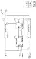
- the DLL integrated circuit 200is illustrated as including a digital delay line 110 that is configured to generate an internal clock signal ICLK in response to a reference clock signal REF, which may have a non-unity duty cycle.
- the digital delay line 110may comprise a plurality of delay units that collectively establish the total delay provided by the delay line 110 .
- the delay units(not shown) may provide a variable delay that is controlled by a value of a control signal (CNTL), which is generated by a delay line control circuit 120 .
- CNTLcontrol signal
- each of the delay unitsmay provide a fixed delay, with the number of active delay units within the delay line 110 being controlled by the value of the control signal CNTL generated by the delay line control circuit 120 .
- This control signal CNTLmay be a multi-bit digital signal. Exemplary delay lines are illustrated and described in commonly assigned U.S. patent application Ser. Nos. 10/643,208, filed Aug. 18, 2003, and Ser. No. 10/663,624, filed Sep. 16, 2003, the disclosures of which are hereby incorporated herein by reference.
- the DLL integrated circuit 200is also illustrated as including a phase comparator 100 , which is responsive to the reference clock signal REF and a feedback clock signal FB.
- the feedback clock signal FBtypically represents a delayed version of the internal clock signal ICLK, with the degree of delay being provided by a fixed delay unit 130 that is configured to receive the internal clock signal ICLK.
- the reference clock signal REF and the feedback clock signal FBwill be in-phase with each other when a total delay provided by the digital delay line 110 and the fixed delay unit 130 equals an integer multiple of the period of the reference clock signal REF.
- the phase comparator 100is also illustrated as being responsive to a power-up signal PWU and a reset signal RESET.
- the reset signal RESETis an active high pulse that is used to reset a second clock divider 20 b , which is responsive to the reference clock signal REF.
- the phase comparator 100is also illustrated as generating four output signals. These four output signals include the compare signal COMP, the lock signal LOCK, the period value signal PERHOLD[ 0 : 5 ] and the shift value signal SHIFTVAL[ 0 : 6 ].
- the compare signal COMPoperates to slow down FB relative to REF or speed up FB relative to REF. As described herein, when the compare signal COMP is set to a logic 1 value, the DLL integrated circuit 200 will operate to slow FB down, and when the compare signal COMP is set to a logic 0 value, the DLL integrated circuit 200 will operate to speed FB up.
- the lock signal LOCKspecifies whether or not the reference and feedback clock signals REF and FB are in-phase.
- the period value signal PERHOLD[ 0 : 5 ], where PERHOLD[ 5 ] is the most significant bit,is the encoded size of one period (T) of the reference clock signal REF.
- the shift value signal SHIFTVAL[ 0 : 6 ]is the encoded value of the amount of delay that the DLL integrated circuit 200 must shift the feedback clock signal FB (in the direction indicated by the compare signal COMP) to lock FB in phase with REF.
- the delay line control circuit 120is responsive to the signals generated by the phase comparator 100 .
- the delay line control circuit 120is configured to adjust a value of the control signal CNTL upwards or downwards in response to the value of the compare signal COMP generated by the phase comparator 100 .
- the magnitude of the initial adjustment that is made to the value of the control signal CNTL (after power-up)is typically controlled by the value of the shift value signal SHIFTVAL[ 0 : 6 ], with adjustments continuing thereafter, if necessary, until the lock signal LOCK indicates phase lock between REF and FB.
- the delay line control circuit 120may be configured to adjust the value of the control signal CNTL so that the phase of the internal clock signal ICLK (and FB) jumps by a phase amount specified by the value of the shift value signal SHIFTVAL[ 0 : 6 ].
- the delay line control circuit 120may also operate to respond to the value of the period value signal PERHOLD[ 0 : 5 ] by generating additional control signals (not shown) that enable the DLL integrated circuit 200 to generate DLL phase delayed output signals for additional applications.
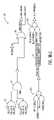
- FIG. 1Billustrates an embodiment of the phase comparator 100 illustrated by FIG. 1A .
- the logic required to generate the period value signal PERHOLD[ 0 : 5 ]includes a pair of negative edge triggered D-type flip-flops (NET DFF) 10 a and 10 b , a positive edge triggered D-type flip-flop (PET DFF) 12 a , a NOR gate 14 and a 6-bit counter 40 a , which is also illustrated and described in U.S. Provisional Application Ser. No. 60/534,381, filed Jan. 5, 2004.
- Each of the D-type flip-flopsincludes a data input (D), a true output (Q) and a complementary output (NQ).
- the three D-type flip-flops 10 a , 10 b and 12 acollectively generate a three-bit period position signal PERPOS[ 0 : 2 ] and a three-bit not period position signal NPERPOS[ 0 : 2 ].
- the NOR gate 14generates a period time signal PERTIME in response to the signals PERPOS 1 and NPERPOS 0 .
- the 6-bit counter 40 aincludes a clock input (CLKDBY 3 ), an enable input (ENABLE), a not enable input (NENABLE), a 3-bit not position input NPOS[ 0 : 2 ] and a 3-bit position input POS[ 0 : 2 ].
- the 6-bit counter 40 agenerates a 6-bit hold count signal HOLDCNT[ 0 : 5 ] and a 6-bit not hold count signal NHOLDCNT[ 0 : 5 ].
- the logic required to generate the compare signal COMPincludes a pair of clock dividers 20 a and 20 b (i.e., divide-by-3 clock generators), which are synchronized with the feedback and reference clock signals FB and REF, respectively, and a pair of phase half-comparators 30 a and 30 b , which are illustrated in greater detail by FIG. 2 .
- the first clock divider 20 agenerates the signal FBDIV 3 at its output (CLKDIV 3 ).
- the signal FBDIV 3is a periodic signal that is synchronized with the feedback clock signal FB and has a period that is three times a period of the feedback clock signal FB.
- the second clock divider 20 bgenerates the signal REFDIV 3 at its output (CLKDIV 3 ).
- the signal REFDIV 3is a periodic signal that is synchronized with the reference clock signal REF and has a period that is three times a period of the reference clock signal REF.
- the combination of REF and REFDIV 3is used to count the amount of time from the falling edge of REF to the falling edge of FB.
- Each of the phase half-comparators 30 a and 30 bhas three input terminals FB, FBDIV 3 and REF and four output terminals COMP, LOCK, NREFHOLD[ 0 : 5 ] and REFHOLD[ 0 : 5 ].
- the first phase half-comparator 30 agenerates the signals COMPREFTOFB, LOCKREFTOFB, and NREFHOLD[ 0 : 5 ] and the second phase half-comparator 30 b generates the signals LOCKFBTOREF and FBHOLD[ 0 : 5 ].
- a first AND-OR logic circuit 50 agenerates the compare signal COMP in response to the compare output COMP of the first phase half-comparator 30 a , the complementary signals NUSECNTCMP (not use count compare) and USECNTCMP (use count compare) and a carry signal CAR 5 .
- the compare output COMPreflects the value of COMPREFTOFB. As described more fully herein, this means the rising edge of FB is simply used to capture the current value of REF when performing the compare operation.
- the signals NUSECNTCMP and USECNTCMPare generated by the logic illustrated by FIG. 1B.2 .
- This logicwhich includes the NOR gates 22 , 24 and 28 and NAND gate 26 , is responsive to a multi-bit result signal RESULT[ 0 : 5 ], a most significant bit of a multi-bit period carry signal PERCAR[ 0 : 5 ] and a most significant bit of a multi-bit carry signal CAR[ 0 : 5 ].
- the phase comparator 100uses a conventional phase comparison method (i.e., an edge comparison method) to generate the compare signal COMP because the period of the reference clock signal REF is too small for the preferred counting phase comparison method to be effective.
- the shift value signal SHIFTVAL[0:6]is also set to 1000000, which is the smallest delay value the DLL integrated circuit 200 can shift the feedback clock signal FB in time by.
- the shift value signal SHIFTVAL[ 0 : 6 ]is equal to the shortest phase difference between the rising edges of FB and REF.
- the carry signal CAR[ 0 : 5 ] and the result signal RESULT[ 0 : 5 ]are generated by a second ripple carry adder 60 b and the period carry signal PERCAR[ 0 : 5 ] is generated by a first ripple carry adder 60 a .
- These ripple carry adders 60 a and 60 binclude first and second comparand inputs IN 0 and IN 1 and a carry input CIN and generate a carry output COUT and a sum output SUM.
- the first and second ripple carry adders 60 a and 60 bare 6-bit adders, which are also illustrated and described in the aforementioned '381 application.
- the second ripple carry adder 60 bis configured to operate as a subtractor that uses count comparisons to determine the shortest route to phase lock.
- the second ripple carry adder 60 boperates to compare REFHOLD[ 0 : 5 ] to FBHOLD[ 0 : 5 ] and uses the conventional phase comparison method when these signals are equal. If they are not equal, the smaller value of the two becomes the smallest phase difference between FB and REF, which is reflected in the value of TERHOLD[ 0 : 5 ].
- the conventional phase comparison methode.g., edge comparison method
- the lock signal LOCKis generated by logically ORing the pair of lock signals generated by the phase half-comparators 30 a and 30 b , which are shown as LOCKREFTOFB and LOCKFBTOREF. Operations to generate these lock signals will be described more fully hereinbelow with reference to FIGS. 3A–3C .
- the shift value signal SHIFTVAL[ 0 : 6 ]is generated by a x7 AND-OR logic circuit 50 b .
- This ternary-to-binary converter 70takes bits that have absolute weights of 3 ⁇ 2 n and converts them to bits that have absolute weights of 2 n .
- the ternary hold signal TERHOLD[ 0 : 5 ]is generated by a x6 AND-OR logic circuit 50 c , which is responsive to the 6-bit reference hold signal REFHOLD[ 0 : 5 ], the carry signal CAR 5 and the feedback hold signal FBHOLD[ 0 : 5 ].
- the reference hold signal REFHOLD[ 0 : 5 ]is generated by the first phase half-comparator 30 a and the feedback hold signal FBHOLD[ 0 : 5 ] is generated by the second phase half-comparator 30 b.
- a phase half-comparator 30is illustrated as including three NET DFFs 10 c – 10 e , four PET DFFs 12 b – 12 e , a pair of NOR gates 32 and 34 and a 6-bit counter 40 b .
- the NET DFF 10 creceives the FBDIV 3 signal at its data input D and generates a feedback position signal FBPOS.
- the NET DFF 10 dreceives the FBDIV 3 signal at its data input D and generates the reference position 0 signal REFPOS 0 and the not reference position 0 signal NREFPOSO.
- the NET DFF 10 ereceives the REFPOS 0 signal at its data input D and generates the reference position 1 signal REFPOS 1 and the not reference position 1 signal NREFPOS 1 .
- the NOR gate 32generates a reference time signal REFTIME in response to FBPOS, NREFPOS 0 and REFPOS 1 .
- the 6-bit counter 40 bWhen this reference time signal REFTIME is active at a high level, the 6-bit counter 40 b is enabled to perform count operations.
- the PET DFF 12 breceives the reference clock signal REF at its data input D and generates a reference beginning signal QREFBEG.
- the PET DFF 12 creceives the FBDIV 3 signal at its data input D and generates the reference position 2 signal REFPOS 2 at its true output Q and the not reference position 2 signal NREFPOS 2 at its complementary output NQ.
- the PET DFF 12 dis synchronized with the signal NFB, which is an inverted version of the feedback clock signal FB.
- the PET DFF 12 dreceives the reference clock signal REF at its data input D and generates a reference midpoint signal QREFMID.
- the PET DFF 12 ereceives the reference clock signal REF at its data input D and generates the not reference end signal NQREFEND at its complementary output NQ.
- the PET DFF 12 eis synchronized with a delayed feedback clock signal FBD.
- the NOR gate 34generates a lock signal LOCK for the phase half-comparator 30 .
- This NOR gate 34is responsive to the reference beginning signal QREFBEG and the not reference end signal NQREFEND.
- the 6-bit counter 40 bgenerates the 6-bit reference hold signal REFHOLD[ 0 : 5 ] and the 6-bit not reference hold NREFHOLD signal NREFHOLD[ 0 : 5 ] for the phase half-comparator 30 .
- the timing of the above-described signals FBDIV 3 , FB, REF, REFTIME, REFPOS[ 0 : 2 ] and FBPOS within the phase half-comparator 30are also illustrated by FIG. 13 of the aforementioned '318 application.
- the phase comparator 100is illustrated as being responsive to first and second periodic signals (REF and FB) which may have equivalent non-unity duty cycle ratios.
- the phase comparator 100generates a compare signal COMP that identifies a direction the feedback clock signal FB should be shifted in time to bring it into alignment with the reference clock signal REF.
- This compare signal COMPis generated by comparing a first degree to which the reference clock signal REF leads the feedback clock signal FB to a second degree to which the reference clock signal REF lags the feedback clock signal FB.
- phase comparator 100determines a smaller of the first and second degrees and sets the compare signal COMP of FIG. 1A to a value that results in a speed-up of the feedback clock signal FB when the first degree is determined to be less than the second degree.
- the compare signal COMPis set at a value that results in a slow-down of the feedback clock signal FB when the second degree is determined to be less than the first degree.
- the delay line control circuit 120may respond to the shift value signal SHIFTVAL[ 0 : 6 ] by adjusting the value of the control signal CNTL in a single cycle so that the phase of the feedback clock signal FB jumps by an amount sufficient to almost immediately place it into at least close alignment with the reference clock signal REF.
- the lock signal LOCK illustrated in FIG. 1B.1is generated by logically ORing a first lock signal (LOCKREFTOFB), which specifies whether a leading edge of the reference clock signal REF is within a first time window (e.g., a 200 ps time window) relative to a leading edge of the feedback clock signal FB, and a second lock signal (LOCKFBTOREF), which specifies whether the leading edge of the feedback clock signal FB is within a second time window (e.g., 200 ps time window) relative to the leading edge of the reference clock signal REF.
- LOCKREFTOFBa first lock signal
- LOCKFBTOREFsecond lock signal
- FIGS. 3A–3Cillustrate the timing diagrams of FIGS. 3A–3C .
- FIG. 3Aillustrates an ideal case when the reference and feedback clock signals REF and FB are aligned with each other.
- the first and second phase half-comparators 30 a and 30 boperate to identify whether or not the phases of the reference and feedback clock signals are sufficiently aligned to constitute a lock condition.
- a ⁇ 100 ps phase difference between the leading edges of the reference and feedback clock signalsrepresents a lock condition.
- This lock conditionoccurs under two timing scenarios illustrated by FIG. 3A .
- accelerated and delayed versions of the feedback clock signal FBare used to capture the state of the reference clock signal REF as “0” and “1”, respectively.
- These operationsare performed within the first phase half-comparator 30 a , with the reference clock signal REF being provided as a data input to the flip-flops 12 b , 12 d and 12 e .
- the nominal delay provided by an inverterequals 100 ps
- the delayed feedback clock signal FBDwhich is provided to the clock input of PET DFF 12 e
- will be delayed by 200 ps relative to the clock input of PET DFF 12 bwhich receives the feedback clock signal FB.
- the clock signals provided to these two clock inputsare illustrated as PCH_REFTOFB.FB and PCH_REFTOFB.FBD in FIG. 3A , and the first lock signal LOCKREFTOFB is generated at the output of the NOR gate 34 .
- accelerated and delayed versions of the reference clock signal REFare used to capture the state of the feedback clock signal FB as “0” and “1”, respectively.
- These operationsare performed within the second phase half-comparator 30 b , with the feedback clock signal FB being provided as a data input to the flip-flops 12 b , 12 d and 12 e .
- the clock signals provided to the clock inputs of flip-flop 12 b and 12 eare illustrated as PCH_FBTOREF.REF and PCH_FBTOREF.REFD, respectively, in FIG. 3A .
- the second lock signal LOCKFBTOREFis generated at the output of the NOR gate 34 . Accordingly, under this ideal timing condition, both the first and second lock signals LOCKREFTOFB and LOCKFBTOREF will be generated at logic 1 values and passed to an output of the phase comparator 100 as a LOCK signal having an active high level.
- FIG. 3Billustrates a first extreme case when the feedback clock signal FB leads the reference clock signal REF by 100 ps.
- the first and second phase half-comparators 30 a and 30 boperate to identify whether or not the phases of the reference and feedback clock signals are sufficiently aligned to constitute a lock condition.
- the determination of this lock conditionoccurs under two timing scenarios illustrated by FIG. 3B .
- Under the first timing scenarioaccelerated and delayed versions of the feedback clock signal FB are used to capture the state of the reference clock signal REF as “0” and “0”, respectively.
- These operationsare performed within the first phase half-comparator 30 a , with the reference clock signal REF being provided as a data input to the flip-flops 12 b , 12 d and 12 e .
- the clock signals provided to the clock inputs of flip-flops 12 b and 12 eare illustrated as PCH_REFTOFB.FB and PCH_REFTOFB.FBD, respectively, and the first lock signal LOCKREFTOFB is generated as a logic 0 signal, which indicates a failure to detect a lock condition.
- accelerated and delayed versions of the reference clock signal REFare used to capture the state of the feedback clock signal FB as “0” and “1”, respectively.
- the clock signals provided to the clock inputs of flip-flop 12 b and 12 eare illustrated as PCH_FBTOREF.REF and PCH_FBTOREF.REFD, respectively, in FIG. 3B .
- the second lock signal LOCKFBTOREFis generated as a logic 1 signal to indicate a lock condition. Accordingly, under this first extreme case, the second lock signal LOCKFBTOREF will be generated at a logic 1 value and passed to an output of the phase comparator 100 as a LOCK signal having an active high level.
- FIG. 3Cillustrates a second extreme case when the feedback clock signal FB lags the reference clock signal REF by 100 ps.
- the first and second phase half-comparators 30 a and 30 boperate to identify whether or not the phases of the reference and feedback clock signals are sufficiently aligned to constitute a lock condition.
- the determination of this lock conditionoccurs under two timing scenarios illustrated by FIG. 3C .
- Under the first timing scenarioaccelerated and delayed versions of the feedback clock signal FB are used to capture the state of the reference clock signal REF as “0” and “1”, respectively.
- the operationsare performed within the first phase half-comparator 30 a , with the reference clock signal REF being provided as a data input to the flip-flops 12 b , 12 d and 12 e .
- the clock signals provided to the clock inputs of flip-flops 12 b and 12 eare illustrated as PCH_REFTOFB.FB and PCH_REFTOFB.FBD, respectively, and the first lock signal LOCKREFTOFB is generated as a logic 1 signal, which indicates a lock condition.
- accelerated and delayed versions of the reference clock signal REFare used to capture the state of the feedback clock signal FB as “0” and “0”, respectively.
- the second phase half-comparator 30 bThese operations are performed within the second phase half-comparator 30 b , with the feedback clock signal FB being provided as a data input to the flip-flops 12 b , 12 d and 12 e .
- the clock signals provided to the clock inputs of flip-flop 12 b and 12 eare illustrated as PCH_FBTOREF.REF and PCH_FBTOREF.REFD, respectively, in FIG. 3C .
- the second lock signal LOCKFBTOREFis generated as a logic 0 signal, which indicates a failure to detect a lock condition. Accordingly, under this second extreme case, the first lock signal LOCKREFTOFB will be generated at a logic 1 value and passed to an output of the phase comparator 100 as a LOCK signal having an active high level.
- a delay-locked loop integrated circuit 400includes a delay chain 402 , a phase comparator 404 and a delay chain control circuit 406 , connected as illustrated.
- the delay chain 402is illustrated as a binary-weighted delay chain 402 that is configured to receive a periodic signal to be delayed.
- the delay chain 402includes a plurality of delay chain units (DCUs), such as those illustrated in more detail in FIGS. 5A–5C .
- DCUsdelay chain units
- the delay chain control circuit 406may include a control circuit 502 , a buffer register 504 , an adder/subtractor 506 , a priority encoder 508 , a shift register 510 , a delay line decoder 512 and a clock generator/selector circuit 514 , as illustrated by FIG. 5E .
- the periodic signalis illustrated as a reference clock signal that is received at an input (CLKIN) of the delay chain 402 and also received at a first input (REF) of the phase comparator 404 .
- the output (CLKOUT) of the delay chain 402is configured to generate a delayed version of the periodic signal received at the input of the delay chain 402 .
- the delay chain 402is illustrated as generating an output clock signal, which may be provided to circuit elements (not shown) on an integrated circuit chip.
- the output clock signal(or a delayed version thereof) may also be used as a feedback clock signal.
- This feedback clock signalis provided to a second input (FB) of the phase comparator 404 .
- the signal path from the output (CLKOUT) of the delay chain 402 to the second input (FB) of the phase comparator 404may also include a fixed delay device (e.g., fixed delay line), which adds an additional delay to the periodic signal generated at the output of the delay chain 402 .
- a fixed delay devicee.g., fixed delay line
- the phase comparator 404is illustrated as generating a compare signal (COMP) and a lock signal (LOCK).
- the compare signal COMPis configured to identify a leading or lagging relationship between the reference clock signal and the feedback clock signal.
- the lock signal LOCKis configured to indicate whether the reference and feedback clock signals are sufficiently close in phase to be considered phase-locked to each other.
- the delay chain control circuit 406is configured to receive the reference clock signal and the lock and compare signals generated by the phase comparator 404 .
- the delay chain control circuitis also configured to receive a power-up signal (PWU), which is active during a power-up time interval and thereafter inactive, and a reset signal (RESET), which may be used to simply reset a clock generator/selector located internal to the delay chain control circuit 406 .
- the reset signal RESETmay also perform operations similar to the power-up signal.
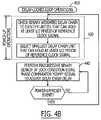
- operations 410 performed by the delay-locked loop integrated circuit 400 of FIG. 4Ainclude power-up operations, Block 420 , and search operations, Block 440 .
- the power-up operations 420are illustrated as including an operation to check the binary-weighted delay chain 402 to identify at least one delay chain unit that can hold a desired fraction of a period of a reference clock signal, which is provided to an input of the delay chain 402 .
- This desired fraction of the periodis preferably set at a value of one-half the period of the reference clock signal, however, other fractions of the period can also be identified.
- the smallest of the identified delay chain unitsis then selected by enabling its delay path within the delay chain 402 and enabling the bypass paths within the remaining delay chain units within the delay chain 402 .
- This selection operationcauses the delay chain 402 to provide a total delay equivalent to about the delay of the selected delay chain unit. This total delay represents a starting point for the search operations illustrated by Block 440 , which occur after the power-up operations are complete.
- the power-up operationsare followed by a progressive binary search operation to a achieve a lock condition within the delay-locked loop integrated circuit 400 .
- the compare signal COMP generated by the phase comparator 404is used by the delay chain control circuit 406 to adjust (+ or ⁇ ) the amount of delay provided by the delay chain 402 .
- the phase comparator 404will generate an active lock signal LOCK, which operates to suspend further adjustments to the delay of the delay chain 402 until the active state of the lock signal LOCK is removed.
- the operations illustrated by Block 440continue until a next power-down/power-up event occurs.
- the power-up operations, Block 420may include an operation to force the delay chain 402 to its halfway point, Block 420 a .
- An operationis also performed to generate a plurality of internal divide-by-N clock signals in response to the reference clock signal, Block 420 b .
- the plurality of divide-by-N clock signalsmay include divide-by-2, divide-by-3, divide-by-4, divide-by-5, divide-by-6, divide-by-8, divide-by-9 and divide-by-10 clock signals, which are synchronized with the reference clock signal.
- These clock signalsallow for the selection of a higher frequency system clock signal as the frequency of the reference clock signal increases and a shorter locking time is required.
- the delay chain 402also generates a multi-bit delay value signal SAME[ 0 : 6 ], Block 420 c .
- This delay value signal SAMEidentifies all of the delay chain units (DCUs) that are configured to provide a delay in excess of one-half the period of the reference clock signal.
- DCUsdelay chain units
- the delay chain units 404 _ 16 , 404 _ 32 and 404 _ 64are configured to provide a delay in excess of one-half the period of a particular reference clock signal, then the multi-bit delay value signal SAME[ 0 : 6 ] may equal [0000111].
- the delay chain control circuit 406selects the smallest delay chain unit from the group identified as providing an excessive delay, Block 420 d . In the specified example, this operation would select the fifth delay chain unit 404 _ 16 .
- This selection operationis performed by the priority encoder 508 , which generates an encoded output signal (not shown) in response to the multi-bit delay value signal SAME, and the delay line decoder 512 , which generates a multi-bit decode signal (not shown) in response to the encoded output signal generated by the priority encoder 508 . These operations are performed under the control of the control circuit 502 .
- Delay preset operationsare then performed by loading the identity of the selected delay chain unit DCU into the buffer register 504 and into the shift register 510 , under the control of the control circuit 502 , Block 420 e .
- This identityis specified by the multi-bit decode signal generated by the delay line decoder 512 .
- the identity of the smallest delay chain unit DCUis also used by the system clock selector 514 to select one of a plurality of divide-by-N clock signals as a system clock signal.
- This system clock signalis used to control timing of operations within the delay chain control circuit 406 , Block 420 f .
- These divide-by-N clock signalsare generated by respective clock generators that receive the reference clock signal as a synchronization signal.
- the selection of the fifth delay chain unit 404 _ 16 during power-upwill cause the system clock signal to have a period equal to 6 ⁇ the period of the reference clock signal.
- the control circuit 502operates to terminate the power-up operations in-sync with the selected system clock signal, Block 420 g , and thereafter the progressive binary search operations commence, Block 440 , at a rate dictated by the selected system clock signal. Accordingly, as the frequency of the reference clock signal increases and a smaller delay chain unit is selected during power-up, the frequency of the system clock signal increases to yield a faster search operation rate and shorter lock time.
- the progressive binary search operationsinclude using the current value stored within the buffer register 504 to set the initial value of the multi-bit delay unit enable signal SW[ 0 : 6 ] generated by the control circuit 502 , Block 440 a .
- the value stored within the shift register 510is then updated to one-half its current value by the control circuit 502 , Block 440 b .
- the phase comparator 404operates to compare the phases of the reference and feedback clock signals, Block 440 c , and a check is made to determine whether a lock condition is present, Block 440 d .
- the value of the compare signal COMPis used by the delay chain control circuit 406 to add/subtract the current value of the shift register 510 to/from the value stored within the buffer register 504 and then the buffer register 504 is updated with this new value, Block 440 e .
- the compare signal COMPis set to a logic 1 value
- an operationmay be performed to add the current value of the shift register 510 to the value stored within the buffer register 504 .
- the compare signalis set to a logic 0 value
- an operationmay be performed to subtract the current value of the shift register 510 from the value stored within the buffer register 504 .
- the output of the buffer register 504may then be used to generate an updated multi-bit delay unit enable signal SW[ 0 : 6 ], Block 440 f .
- This updateis preferably synchronized with the output of the system clock selector 514 , which represents the system clock used by the control circuit 502 .
- the maximum rate of update of the multi-bit delay unit enable signal SW[ 0 : 6 ] during the progressive binary search operationsis a function of the value of the multi-bit delay value signal SAME[0:6] generated during the power-up operations, which is a function of the reference clock signal frequency.
- the shift register 510is then updated with half its current value, Block 440 g , to achieve a next step in the progressive binary search operation. Control is then returned to Block 440 c .
- the operations illustrated by Blocks 440 c – 440 gare then repeated as many times as necessary to achieve a phase-locked condition, Block 440 d.
- the binary-weighted delay chain 402 of FIG. 4Amay include a plurality of delay chain units 404 _ 1 – 404 _ 64 , which are illustrated as being arranged in ascending order according to delay. Other arrangements of the delay chain units within the delay chain 402 are also possible.
- the first two delay chain units 404 _ 1 and 404 _ 2are illustrated more fully by FIG. 5B and the remaining five delay chain units 404 _ 4 – 404 _ 64 are illustrated more fully by FIG. 5C .
- Each of the delay chain units (DCUs)includes a delay path, a bypass path and a built-in phase comparator.
- the delay and bypass pathsinclude first and second inverters I 1 and I 2 , first and second NAND gates ND 1 and ND 2 , a NOR gate NR 1 and a delay element 408 , which is illustrated more fully as a string of inverters in FIG. 5D .
- the bypass pathis enabled when a corresponding bit (i.e., SW[n]) of the multi-bit delay unit enable signal SW[ 0 : 6 ] is set to a logic 0 value and the output of inverter I 1 is switched low-to-high to thereby enable the first NAND gate ND 1 .
- the corresponding delay chain unit DCUis essentially removed from the serial delay path provided by the delay chain 402 .
- the phase comparatorincludes third, fourth and fifth inverters I 3 , I 4 and I 5 , first and second D-type flip-flops FF 1 and FF 2 and a NOR gate NR 2 .
- the signals MID(2 n ⁇ 1) and NMID(2 n ⁇ 1)are derived from an output of the delay element 408 and provided as inputs to the first and second flip-flops FF 1 and FF 2 , as illustrated.
- the input IN to the delay chain unit DCUis provided as a clock input to the flip-flops, which generate signals SM 0 and SM 1 . These signals SM 0 and SM 1 are logically OR'ed to thereby generate a respective bit of the multi-bit delay value signal SAME[ 0 : 6 ]. Based on this configuration of the phase comparator within the delay chain unit DCU, the signal SAME in FIG. 5B is set to a logic 1 value whenever the delay provided by the corresponding delay element 408 is greater than one-half the period of the signal provided to the input IN of the delay chain unit, which equals the period of the reference clock signal received by the delay chain 402 .
- the remaining delay chain units 404 _ 4 – 404 _ 64 of FIG. 5Care similar to the delay chain units illustrated by FIG. 5B , however, the phase comparator illustrated in FIG. 5C includes three D-type flip-flops FF 3 , FF 4 and FF 5 and a three-input NOR gate NR 3 .
- the signal MID(2 (n ⁇ 1) +1)is also used in addition to the signals MID( 2 n ⁇ 1) and NMID(2 n ⁇ 1), which are derived from an output of the delay element 408 . As illustrated by FIG.
- the signal MID(2 (n ⁇ 1) +1)is derived by tapping off a corresponding node in the inverter string within the delay element 408 , where “n” is a positive integer having the values shown by FIG. 5A .
- This inverter stringis illustrated as including the inverters INVM 0 –INVM(2 n ⁇ 1).
Landscapes
- Engineering & Computer Science (AREA)
- Power Engineering (AREA)
- Physics & Mathematics (AREA)
- Nonlinear Science (AREA)
- Stabilization Of Oscillater, Synchronisation, Frequency Synthesizers (AREA)
Abstract
Description
Claims (7)
Priority Applications (2)
| Application Number | Priority Date | Filing Date | Title |
|---|---|---|---|
| US10/891,919US7119591B1 (en) | 2004-01-05 | 2004-07-15 | Delay-locked loop (DLL) integrated circuits having binary-weighted delay chain units with built-in phase comparators that support efficient phase locking |
| US11/532,657US7279938B1 (en) | 2004-01-05 | 2006-09-18 | Delay chain integrated circuits having binary-weighted delay chain units with built-in phase comparators therein |
Applications Claiming Priority (3)
| Application Number | Priority Date | Filing Date | Title |
|---|---|---|---|
| US53431804P | 2004-01-05 | 2004-01-05 | |
| US10/880,804US7109760B1 (en) | 2004-01-05 | 2004-06-30 | Delay-locked loop (DLL) integrated circuits that support efficient phase locking of clock signals having non-unity duty cycles |
| US10/891,919US7119591B1 (en) | 2004-01-05 | 2004-07-15 | Delay-locked loop (DLL) integrated circuits having binary-weighted delay chain units with built-in phase comparators that support efficient phase locking |
Related Parent Applications (1)
| Application Number | Title | Priority Date | Filing Date |
|---|---|---|---|
| US10/880,804Continuation-In-PartUS7109760B1 (en) | 2004-01-05 | 2004-06-30 | Delay-locked loop (DLL) integrated circuits that support efficient phase locking of clock signals having non-unity duty cycles |
Related Child Applications (1)
| Application Number | Title | Priority Date | Filing Date |
|---|---|---|---|
| US11/532,657DivisionUS7279938B1 (en) | 2004-01-05 | 2006-09-18 | Delay chain integrated circuits having binary-weighted delay chain units with built-in phase comparators therein |
Publications (1)
| Publication Number | Publication Date |
|---|---|
| US7119591B1true US7119591B1 (en) | 2006-10-10 |
Family
ID=36974491
Family Applications (2)
| Application Number | Title | Priority Date | Filing Date |
|---|---|---|---|
| US10/880,804Expired - LifetimeUS7109760B1 (en) | 2004-01-05 | 2004-06-30 | Delay-locked loop (DLL) integrated circuits that support efficient phase locking of clock signals having non-unity duty cycles |
| US10/891,919Expired - LifetimeUS7119591B1 (en) | 2004-01-05 | 2004-07-15 | Delay-locked loop (DLL) integrated circuits having binary-weighted delay chain units with built-in phase comparators that support efficient phase locking |
Family Applications Before (1)
| Application Number | Title | Priority Date | Filing Date |
|---|---|---|---|
| US10/880,804Expired - LifetimeUS7109760B1 (en) | 2004-01-05 | 2004-06-30 | Delay-locked loop (DLL) integrated circuits that support efficient phase locking of clock signals having non-unity duty cycles |
Country Status (1)
| Country | Link |
|---|---|
| US (2) | US7109760B1 (en) |
Cited By (54)
| Publication number | Priority date | Publication date | Assignee | Title |
|---|---|---|---|---|
| US20060158274A1 (en)* | 2005-01-19 | 2006-07-20 | Self Paul W R | Circuits and methods of generating and controlling signals on an integrated circuit |
| US20060164141A1 (en)* | 2005-01-21 | 2006-07-27 | Self Paul W R | Controlled delay line circuit with integrated transmission line reference |
| US20060203948A1 (en)* | 2005-03-14 | 2006-09-14 | Micron Technology, Inc. | Phase detector and method providing rapid locking of delay-lock loops |
| US20060261871A1 (en)* | 2004-08-20 | 2006-11-23 | Eric Becker | Delay circuit with reset-based forward path static delay |
| US20070002675A1 (en)* | 2005-06-30 | 2007-01-04 | Koo Cheul H | Synchronous memory device with output driver controller |
| US20070035351A1 (en)* | 2005-01-19 | 2007-02-15 | Self Paul W R | Fully integrated frequency generator |
| US7287235B1 (en)* | 2004-08-06 | 2007-10-23 | Calypto Design Systems, Inc. | Method of simplifying a circuit for equivalence checking |
| US20080144423A1 (en)* | 2006-12-19 | 2008-06-19 | Jongtae Kwak | Timing synchronization circuit with loop counter |
| US20080232179A1 (en)* | 2007-03-15 | 2008-09-25 | Micron Technology, Inc. | Circuit, system and method for controlling read latency |
| US20090015302A1 (en)* | 2007-07-12 | 2009-01-15 | Hynix Semiconductor Inc. | Delay locked loop and method of controlling the same |
| US20140359089A1 (en)* | 2009-10-30 | 2014-12-04 | Iii Holdings 2, Llc | Network proxy for high-performance, low-power data center interconnect fabric |
| US8913448B2 (en) | 2012-10-25 | 2014-12-16 | Micron Technology, Inc. | Apparatuses and methods for capturing data in a memory |
| US8984320B2 (en) | 2011-03-29 | 2015-03-17 | Micron Technology, Inc. | Command paths, apparatuses and methods for providing a command to a data block |
| US9001594B2 (en) | 2012-07-06 | 2015-04-07 | Micron Technology, Inc. | Apparatuses and methods for adjusting a path delay of a command path |
| US9000817B2 (en) | 2012-02-01 | 2015-04-07 | Micron Technology, Inc. | Apparatuses and methods for altering a forward path delay of a signal path |
| US9054675B2 (en) | 2012-06-22 | 2015-06-09 | Micron Technology, Inc. | Apparatuses and methods for adjusting a minimum forward path delay of a signal path |
| US9166579B2 (en) | 2012-06-01 | 2015-10-20 | Micron Technology, Inc. | Methods and apparatuses for shifting data signals to match command signal delay |
| US9262225B2 (en) | 2009-10-30 | 2016-02-16 | Iii Holdings 2, Llc | Remote memory access functionality in a cluster of data processing nodes |
| US9329623B2 (en) | 2012-08-22 | 2016-05-03 | Micron Technology, Inc. | Apparatuses, integrated circuits, and methods for synchronizing data signals with a command signal |
| US9465771B2 (en) | 2009-09-24 | 2016-10-11 | Iii Holdings 2, Llc | Server on a chip and node cards comprising one or more of same |
| US9479463B2 (en) | 2009-10-30 | 2016-10-25 | Iii Holdings 2, Llc | System and method for data center security enhancements leveraging managed server SOCs |
| US9508417B2 (en) | 2014-02-20 | 2016-11-29 | Micron Technology, Inc. | Methods and apparatuses for controlling timing paths and latency based on a loop delay |
| US9509552B2 (en) | 2009-10-30 | 2016-11-29 | Iii Holdings 2, Llc | System and method for data center security enhancements leveraging server SOCs or server fabrics |
| US9530473B2 (en) | 2014-05-22 | 2016-12-27 | Micron Technology, Inc. | Apparatuses and methods for timing provision of a command to input circuitry |
| US9531363B2 (en) | 2015-04-28 | 2016-12-27 | Micron Technology, Inc. | Methods and apparatuses including command latency control circuit |
| US9585281B2 (en) | 2011-10-28 | 2017-02-28 | Iii Holdings 2, Llc | System and method for flexible storage and networking provisioning in large scalable processor installations |
| US9601170B1 (en) | 2016-04-26 | 2017-03-21 | Micron Technology, Inc. | Apparatuses and methods for adjusting a delay of a command signal path |
| US9648102B1 (en) | 2012-12-27 | 2017-05-09 | Iii Holdings 2, Llc | Memcached server functionality in a cluster of data processing nodes |
| US9680770B2 (en) | 2009-10-30 | 2017-06-13 | Iii Holdings 2, Llc | System and method for using a multi-protocol fabric module across a distributed server interconnect fabric |
| US9792249B2 (en) | 2011-10-31 | 2017-10-17 | Iii Holdings 2, Llc | Node card utilizing a same connector to communicate pluralities of signals |
| US9813067B2 (en) | 2015-06-10 | 2017-11-07 | Micron Technology, Inc. | Clock signal and supply voltage variation tracking |
| US9865317B2 (en) | 2016-04-26 | 2018-01-09 | Micron Technology, Inc. | Methods and apparatuses including command delay adjustment circuit |
| US9876735B2 (en) | 2009-10-30 | 2018-01-23 | Iii Holdings 2, Llc | Performance and power optimized computer system architectures and methods leveraging power optimized tree fabric interconnect |
| US9997220B2 (en) | 2016-08-22 | 2018-06-12 | Micron Technology, Inc. | Apparatuses and methods for adjusting delay of command signal path |
| TWI634747B (en)* | 2017-01-13 | 2018-09-01 | 國立中山大學 | Delay-locked loop |
| US10140245B2 (en) | 2009-10-30 | 2018-11-27 | Iii Holdings 2, Llc | Memcached server functionality in a cluster of data processing nodes |
| US10224938B2 (en) | 2017-07-26 | 2019-03-05 | Micron Technology, Inc. | Apparatuses and methods for indirectly detecting phase variations |
| US10877695B2 (en) | 2009-10-30 | 2020-12-29 | Iii Holdings 2, Llc | Memcached server functionality in a cluster of data processing nodes |
| US11031924B1 (en)* | 2019-12-25 | 2021-06-08 | Nuvoton Technology Corporation | Clock multiplier |
| US20220085818A1 (en)* | 2019-03-26 | 2022-03-17 | Lapis Semiconductor Co., Ltd. | Semiconductor device |
| US11467883B2 (en) | 2004-03-13 | 2022-10-11 | Iii Holdings 12, Llc | Co-allocating a reservation spanning different compute resources types |
| US11494235B2 (en) | 2004-11-08 | 2022-11-08 | Iii Holdings 12, Llc | System and method of providing system jobs within a compute environment |
| US11496415B2 (en) | 2005-04-07 | 2022-11-08 | Iii Holdings 12, Llc | On-demand access to compute resources |
| US11522952B2 (en) | 2007-09-24 | 2022-12-06 | The Research Foundation For The State University Of New York | Automatic clustering for self-organizing grids |
| US11630704B2 (en) | 2004-08-20 | 2023-04-18 | Iii Holdings 12, Llc | System and method for a workload management and scheduling module to manage access to a compute environment according to local and non-local user identity information |
| US11650857B2 (en) | 2006-03-16 | 2023-05-16 | Iii Holdings 12, Llc | System and method for managing a hybrid computer environment |
| US11652706B2 (en) | 2004-06-18 | 2023-05-16 | Iii Holdings 12, Llc | System and method for providing dynamic provisioning within a compute environment |
| US11658916B2 (en) | 2005-03-16 | 2023-05-23 | Iii Holdings 12, Llc | Simple integration of an on-demand compute environment |
| US11720290B2 (en) | 2009-10-30 | 2023-08-08 | Iii Holdings 2, Llc | Memcached server functionality in a cluster of data processing nodes |
| US11960937B2 (en) | 2004-03-13 | 2024-04-16 | Iii Holdings 12, Llc | System and method for an optimizing reservation in time of compute resources based on prioritization function and reservation policy parameter |
| US12120040B2 (en) | 2005-03-16 | 2024-10-15 | Iii Holdings 12, Llc | On-demand compute environment |
| US12119830B2 (en) | 2023-03-13 | 2024-10-15 | Apple Inc. | Systems and methods for PLL gain calibration and duty cycle calibration using shared phase detector |
| US12132490B2 (en) | 2023-03-13 | 2024-10-29 | Apple Inc. | Systems and methods for PLL gain calibration |
| US12231132B2 (en) | 2023-03-13 | 2025-02-18 | Apple Inc. | Systems and methods for PLL duty cycle calibration |
Citations (33)
| Publication number | Priority date | Publication date | Assignee | Title |
|---|---|---|---|---|
| US5317219A (en) | 1991-09-30 | 1994-05-31 | Data Delay Devices, Inc. | Compensated digital delay circuit |
| US5374860A (en) | 1993-01-15 | 1994-12-20 | National Semiconductor Corporation | Multi-tap digital delay line |
| US5485490A (en) | 1992-05-28 | 1996-01-16 | Rambus, Inc. | Method and circuitry for clock synchronization |
| US5515403A (en)* | 1994-06-21 | 1996-05-07 | Dsc Communications Corporation | Apparatus and method for clock alignment and switching |
| US5561692A (en) | 1993-12-09 | 1996-10-01 | Northern Telecom Limited | Clock phase shifting method and apparatus |
| US5614855A (en) | 1994-02-15 | 1997-03-25 | Rambus, Inc. | Delay-locked loop |
| US5719515A (en) | 1993-09-27 | 1998-02-17 | Sgs-Thomson Microelectronics S.A. | Digital delay line |
| US5818769A (en) | 1996-11-26 | 1998-10-06 | Tweed; David B. | Dynamically variable digital delay line |
| US5828257A (en) | 1995-09-08 | 1998-10-27 | International Business Machines Corporation | Precision time interval division with digital phase delay lines |
| US5844954A (en) | 1993-02-17 | 1998-12-01 | Texas Instruments Incorporated | Fine resolution digital delay line with coarse and fine adjustment stages |
| US5847616A (en) | 1996-12-12 | 1998-12-08 | Tritech Microelectronics International, Ltd. | Embedded voltage controlled oscillator with minimum sensitivity to process and supply |
| US5910740A (en) | 1997-06-18 | 1999-06-08 | Raytheon Company | Phase locked loop having memory |
| US6125157A (en) | 1997-02-06 | 2000-09-26 | Rambus, Inc. | Delay-locked loop circuitry for clock delay adjustment |
| US6134180A (en) | 1998-08-04 | 2000-10-17 | Samsung Electronics, Co., Ltd. | Synchronous burst semiconductor memory device |
| US6194937B1 (en) | 1997-10-06 | 2001-02-27 | Nec Corporation | Synchronous delay circuit system |
| US6239892B1 (en) | 1998-05-31 | 2001-05-29 | Sun Microsystems, Inc. | Method and apparatus for bit synchronization in optical communication and networking systems |
| US6255969B1 (en) | 1997-12-18 | 2001-07-03 | Advanced Micro Devices, Inc. | Circuit and method for high speed bit stream capture using a digital delay line |
| US6275899B1 (en) | 1998-11-13 | 2001-08-14 | Creative Technology, Ltd. | Method and circuit for implementing digital delay lines using delay caches |
| US6285172B1 (en) | 2000-11-13 | 2001-09-04 | Texas Instruments Incorporated | Digital phase-locked loop circuit with reduced phase jitter frequency |
| US6285229B1 (en) | 1999-12-23 | 2001-09-04 | International Business Machines Corp. | Digital delay line with low insertion delay |
| US6288574B1 (en) | 1999-12-21 | 2001-09-11 | Xerox Corporation | Digital phase detector |
| US6313676B1 (en) | 1999-03-16 | 2001-11-06 | Kabushiki Kaisha Toshiba | Synchronous type semiconductor integrated circuit having a delay monitor controlled by a delay control signal obtained in a delay measuring mode |
| US6313621B1 (en) | 1997-09-16 | 2001-11-06 | Siemens Aktiengesellschaft | Method and arrangement for determining the phase difference between two timing signals |
| US6348827B1 (en) | 2000-02-10 | 2002-02-19 | International Business Machines Corporation | Programmable delay element and synchronous DRAM using the same |
| US6356099B1 (en) | 1994-11-10 | 2002-03-12 | Advanced Micro Devices, Inc. | Transmission-line-noise immune input buffer |
| US6356158B1 (en) | 2000-05-02 | 2002-03-12 | Xilinx, Inc. | Phase-locked loop employing programmable tapped-delay-line oscillator |
| US6359489B1 (en) | 2000-10-05 | 2002-03-19 | Silicon Integrated Systems Corp. | Clock signal generation and buffer circuit having high noise immunity and low power consumption |
| US6366150B1 (en) | 1997-05-23 | 2002-04-02 | Mitsubishi Denki Kabushiki Kaisha | Digital delay line |
| US6411142B1 (en) | 2000-12-06 | 2002-06-25 | Ati International, Srl | Common bias and differential structure based DLL with fast lockup circuit and current range calibration for process variation |
| US6424228B1 (en) | 1997-10-13 | 2002-07-23 | Samsung Electronics Co., Ltd. | Stabilized phase lock detection circuits and methods of operation therefor |
| US6469493B1 (en)* | 1995-08-01 | 2002-10-22 | Teradyne, Inc. | Low cost CMOS tester with edge rate compensation |
| US6477110B2 (en) | 2001-03-09 | 2002-11-05 | Samsung Electronics Co., Ltd. | Semiconductor memory device having different data rates in read operation and write operation |
| US6664838B1 (en) | 2001-08-31 | 2003-12-16 | Integrated Device Technology, Inc. | Apparatus and method for generating a compensated percent-of-clock period delay signal |
Family Cites Families (7)
| Publication number | Priority date | Publication date | Assignee | Title |
|---|---|---|---|---|
| US5121010A (en)* | 1991-02-14 | 1992-06-09 | Motorola, Inc. | Phase detector with deadzone window |
| JPH0818991A (en)* | 1994-06-30 | 1996-01-19 | Mitsubishi Denki Semiconductor Software Kk | Sampling circuit, phase reference detection circuit, and sampling clock moving circuit |
| TW538597B (en)* | 1998-03-31 | 2003-06-21 | Fujitsu General Co Ltd | Phase lock loop circuit |
| US6265902B1 (en)* | 1999-11-02 | 2001-07-24 | Ericsson Inc. | Slip-detecting phase detector and method for improving phase-lock loop lock time |
| US6622255B1 (en)* | 2000-09-13 | 2003-09-16 | Intel Corporation | Digital clock skew detection and phase alignment |
| US6556489B2 (en)* | 2001-08-06 | 2003-04-29 | Micron Technology, Inc. | Method and apparatus for determining digital delay line entry point |
| KR100520657B1 (en)* | 2003-03-19 | 2005-10-13 | 주식회사 하이닉스반도체 | Phase Comparator for DLL(Delay Locked Loop) |
- 2004
- 2004-06-30USUS10/880,804patent/US7109760B1/ennot_activeExpired - Lifetime
- 2004-07-15USUS10/891,919patent/US7119591B1/ennot_activeExpired - Lifetime
Patent Citations (36)
| Publication number | Priority date | Publication date | Assignee | Title |
|---|---|---|---|---|
| US5317219A (en) | 1991-09-30 | 1994-05-31 | Data Delay Devices, Inc. | Compensated digital delay circuit |
| US5485490A (en) | 1992-05-28 | 1996-01-16 | Rambus, Inc. | Method and circuitry for clock synchronization |
| US5374860A (en) | 1993-01-15 | 1994-12-20 | National Semiconductor Corporation | Multi-tap digital delay line |
| US5844954A (en) | 1993-02-17 | 1998-12-01 | Texas Instruments Incorporated | Fine resolution digital delay line with coarse and fine adjustment stages |
| US5719515A (en) | 1993-09-27 | 1998-02-17 | Sgs-Thomson Microelectronics S.A. | Digital delay line |
| US5561692A (en) | 1993-12-09 | 1996-10-01 | Northern Telecom Limited | Clock phase shifting method and apparatus |
| US5614855A (en) | 1994-02-15 | 1997-03-25 | Rambus, Inc. | Delay-locked loop |
| US5515403A (en)* | 1994-06-21 | 1996-05-07 | Dsc Communications Corporation | Apparatus and method for clock alignment and switching |
| US6356099B1 (en) | 1994-11-10 | 2002-03-12 | Advanced Micro Devices, Inc. | Transmission-line-noise immune input buffer |
| US6469493B1 (en)* | 1995-08-01 | 2002-10-22 | Teradyne, Inc. | Low cost CMOS tester with edge rate compensation |
| US5828257A (en) | 1995-09-08 | 1998-10-27 | International Business Machines Corporation | Precision time interval division with digital phase delay lines |
| US5818769A (en) | 1996-11-26 | 1998-10-06 | Tweed; David B. | Dynamically variable digital delay line |
| US5923597A (en) | 1996-11-26 | 1999-07-13 | Harris Corporation | Dynamically variable digital delay line |
| US5847616A (en) | 1996-12-12 | 1998-12-08 | Tritech Microelectronics International, Ltd. | Embedded voltage controlled oscillator with minimum sensitivity to process and supply |
| US6125157A (en) | 1997-02-06 | 2000-09-26 | Rambus, Inc. | Delay-locked loop circuitry for clock delay adjustment |
| US6539072B1 (en) | 1997-02-06 | 2003-03-25 | Rambus, Inc. | Delay locked loop circuitry for clock delay adjustment |
| US6366150B1 (en) | 1997-05-23 | 2002-04-02 | Mitsubishi Denki Kabushiki Kaisha | Digital delay line |
| US5910740A (en) | 1997-06-18 | 1999-06-08 | Raytheon Company | Phase locked loop having memory |
| US6313621B1 (en) | 1997-09-16 | 2001-11-06 | Siemens Aktiengesellschaft | Method and arrangement for determining the phase difference between two timing signals |
| US6194937B1 (en) | 1997-10-06 | 2001-02-27 | Nec Corporation | Synchronous delay circuit system |
| US6424228B1 (en) | 1997-10-13 | 2002-07-23 | Samsung Electronics Co., Ltd. | Stabilized phase lock detection circuits and methods of operation therefor |
| US6255969B1 (en) | 1997-12-18 | 2001-07-03 | Advanced Micro Devices, Inc. | Circuit and method for high speed bit stream capture using a digital delay line |
| US6239892B1 (en) | 1998-05-31 | 2001-05-29 | Sun Microsystems, Inc. | Method and apparatus for bit synchronization in optical communication and networking systems |
| US6134180A (en) | 1998-08-04 | 2000-10-17 | Samsung Electronics, Co., Ltd. | Synchronous burst semiconductor memory device |
| US6275899B1 (en) | 1998-11-13 | 2001-08-14 | Creative Technology, Ltd. | Method and circuit for implementing digital delay lines using delay caches |
| US6313676B1 (en) | 1999-03-16 | 2001-11-06 | Kabushiki Kaisha Toshiba | Synchronous type semiconductor integrated circuit having a delay monitor controlled by a delay control signal obtained in a delay measuring mode |
| US6288574B1 (en) | 1999-12-21 | 2001-09-11 | Xerox Corporation | Digital phase detector |
| US6285229B1 (en) | 1999-12-23 | 2001-09-04 | International Business Machines Corp. | Digital delay line with low insertion delay |
| US6348827B1 (en) | 2000-02-10 | 2002-02-19 | International Business Machines Corporation | Programmable delay element and synchronous DRAM using the same |
| US6400202B1 (en) | 2000-02-10 | 2002-06-04 | International Business Machines Corporation | Programmable delay element and synchronous DRAM using the same |
| US6356158B1 (en) | 2000-05-02 | 2002-03-12 | Xilinx, Inc. | Phase-locked loop employing programmable tapped-delay-line oscillator |
| US6359489B1 (en) | 2000-10-05 | 2002-03-19 | Silicon Integrated Systems Corp. | Clock signal generation and buffer circuit having high noise immunity and low power consumption |
| US6285172B1 (en) | 2000-11-13 | 2001-09-04 | Texas Instruments Incorporated | Digital phase-locked loop circuit with reduced phase jitter frequency |
| US6411142B1 (en) | 2000-12-06 | 2002-06-25 | Ati International, Srl | Common bias and differential structure based DLL with fast lockup circuit and current range calibration for process variation |
| US6477110B2 (en) | 2001-03-09 | 2002-11-05 | Samsung Electronics Co., Ltd. | Semiconductor memory device having different data rates in read operation and write operation |
| US6664838B1 (en) | 2001-08-31 | 2003-12-16 | Integrated Device Technology, Inc. | Apparatus and method for generating a compensated percent-of-clock period delay signal |
Non-Patent Citations (5)
| Title |
|---|
| Dehng et al., Clock-Deskew Buffer Using a SAR-Controlled Delay-Locked Loop, IEEE Journal of Solid-State Circuits, vol. 35, No. 8, Aug. 2000, pp. 1128-1136. |
| Lee et al., "A 2.5 V CMOS Delay-Locked Loop for an 18 Mbit, 500 Megabyte/s DRAM," IEEE Journal of Solid-State Circuits, vol. 29, No. 12, Dec. 1994, pp. 1491-1496. |
| Minami et al., A 1-GHz Portable Digital Delay-Locked Loop with Infinite Phase Capture Ranges, IEICE Trans. Electron., vol. E84-C, No. 2, Feb. 2001, pp. 220-228. |
| Okajima et al., "Digital Delay Locked Loop and Design Technique for High-Speed Synchronous Interface," IEICE Trans. Electron., vol. E79-C, No. 6, Jun. 1996, pp. 798-806. |
| Ryan, Kevin, "DDR SDRAM Functionality and Controller Read Data Capture," Micron Technology, Inc., vol. 8, Issue 3, 1999, pp. 1-24. |
Cited By (104)
| Publication number | Priority date | Publication date | Assignee | Title |
|---|---|---|---|---|
| US11467883B2 (en) | 2004-03-13 | 2022-10-11 | Iii Holdings 12, Llc | Co-allocating a reservation spanning different compute resources types |
| US12124878B2 (en) | 2004-03-13 | 2024-10-22 | Iii Holdings 12, Llc | System and method for scheduling resources within a compute environment using a scheduler process with reservation mask function |
| US11960937B2 (en) | 2004-03-13 | 2024-04-16 | Iii Holdings 12, Llc | System and method for an optimizing reservation in time of compute resources based on prioritization function and reservation policy parameter |
| US12009996B2 (en) | 2004-06-18 | 2024-06-11 | Iii Holdings 12, Llc | System and method for providing dynamic provisioning within a compute environment |
| US11652706B2 (en) | 2004-06-18 | 2023-05-16 | Iii Holdings 12, Llc | System and method for providing dynamic provisioning within a compute environment |
| US7287235B1 (en)* | 2004-08-06 | 2007-10-23 | Calypto Design Systems, Inc. | Method of simplifying a circuit for equivalence checking |
| US20060261871A1 (en)* | 2004-08-20 | 2006-11-23 | Eric Becker | Delay circuit with reset-based forward path static delay |
| US11630704B2 (en) | 2004-08-20 | 2023-04-18 | Iii Holdings 12, Llc | System and method for a workload management and scheduling module to manage access to a compute environment according to local and non-local user identity information |
| US7276947B2 (en)* | 2004-08-20 | 2007-10-02 | Micron Technology, Inc. | Delay circuit with reset-based forward path static delay |
| US11709709B2 (en) | 2004-11-08 | 2023-07-25 | Iii Holdings 12, Llc | System and method of providing system jobs within a compute environment |
| US12039370B2 (en) | 2004-11-08 | 2024-07-16 | Iii Holdings 12, Llc | System and method of providing system jobs within a compute environment |
| US12008405B2 (en) | 2004-11-08 | 2024-06-11 | Iii Holdings 12, Llc | System and method of providing system jobs within a compute environment |
| US11494235B2 (en) | 2004-11-08 | 2022-11-08 | Iii Holdings 12, Llc | System and method of providing system jobs within a compute environment |
| US11537435B2 (en) | 2004-11-08 | 2022-12-27 | Iii Holdings 12, Llc | System and method of providing system jobs within a compute environment |
| US11537434B2 (en) | 2004-11-08 | 2022-12-27 | Iii Holdings 12, Llc | System and method of providing system jobs within a compute environment |
| US11886915B2 (en) | 2004-11-08 | 2024-01-30 | Iii Holdings 12, Llc | System and method of providing system jobs within a compute environment |
| US11861404B2 (en) | 2004-11-08 | 2024-01-02 | Iii Holdings 12, Llc | System and method of providing system jobs within a compute environment |
| US11656907B2 (en) | 2004-11-08 | 2023-05-23 | Iii Holdings 12, Llc | System and method of providing system jobs within a compute environment |
| US11762694B2 (en) | 2004-11-08 | 2023-09-19 | Iii Holdings 12, Llc | System and method of providing system jobs within a compute environment |
| US7375593B2 (en)* | 2005-01-19 | 2008-05-20 | Paul William Ronald Self | Circuits and methods of generating and controlling signals on an integrated circuit |
| US20070035351A1 (en)* | 2005-01-19 | 2007-02-15 | Self Paul W R | Fully integrated frequency generator |
| US7215208B2 (en)* | 2005-01-19 | 2007-05-08 | Paul William Ronald Self | Fully integrated frequency generator |
| US20060158274A1 (en)* | 2005-01-19 | 2006-07-20 | Self Paul W R | Circuits and methods of generating and controlling signals on an integrated circuit |
| US20060164141A1 (en)* | 2005-01-21 | 2006-07-27 | Self Paul W R | Controlled delay line circuit with integrated transmission line reference |
| US7428284B2 (en) | 2005-03-14 | 2008-09-23 | Micron Technology, Inc. | Phase detector and method providing rapid locking of delay-lock loops |
| US20060203948A1 (en)* | 2005-03-14 | 2006-09-14 | Micron Technology, Inc. | Phase detector and method providing rapid locking of delay-lock loops |
| US12120040B2 (en) | 2005-03-16 | 2024-10-15 | Iii Holdings 12, Llc | On-demand compute environment |
| US11658916B2 (en) | 2005-03-16 | 2023-05-23 | Iii Holdings 12, Llc | Simple integration of an on-demand compute environment |
| US12155582B2 (en) | 2005-04-07 | 2024-11-26 | Iii Holdings 12, Llc | On-demand access to compute resources |
| US12160371B2 (en) | 2005-04-07 | 2024-12-03 | Iii Holdings 12, Llc | On-demand access to compute resources |
| US11496415B2 (en) | 2005-04-07 | 2022-11-08 | Iii Holdings 12, Llc | On-demand access to compute resources |
| US11522811B2 (en) | 2005-04-07 | 2022-12-06 | Iii Holdings 12, Llc | On-demand access to compute resources |
| US11831564B2 (en) | 2005-04-07 | 2023-11-28 | Iii Holdings 12, Llc | On-demand access to compute resources |
| US11533274B2 (en) | 2005-04-07 | 2022-12-20 | Iii Holdings 12, Llc | On-demand access to compute resources |
| US11765101B2 (en) | 2005-04-07 | 2023-09-19 | Iii Holdings 12, Llc | On-demand access to compute resources |
| US20070002675A1 (en)* | 2005-06-30 | 2007-01-04 | Koo Cheul H | Synchronous memory device with output driver controller |
| US7511546B2 (en)* | 2005-06-30 | 2009-03-31 | Hynix Semiconductor Inc. | Synchronous memory device with output driver controlller |
| US11650857B2 (en) | 2006-03-16 | 2023-05-16 | Iii Holdings 12, Llc | System and method for managing a hybrid computer environment |
| US7716510B2 (en)* | 2006-12-19 | 2010-05-11 | Micron Technology, Inc. | Timing synchronization circuit with loop counter |
| US8732509B2 (en) | 2006-12-19 | 2014-05-20 | Micron Technology, Inc. | Timing synchronization circuit with loop counter |
| US20080144423A1 (en)* | 2006-12-19 | 2008-06-19 | Jongtae Kwak | Timing synchronization circuit with loop counter |
| US9529379B2 (en) | 2006-12-19 | 2016-12-27 | Micron Technology, Inc. | Timing synchronization circuit with loop counter |
| US20100199117A1 (en)* | 2006-12-19 | 2010-08-05 | Micron Technology, Inc. | Timing synchronization circuit with loop counter |
| US8018791B2 (en) | 2007-03-15 | 2011-09-13 | Micron Technology, Inc. | Circuit, system and method for controlling read latency |
| US10658019B2 (en) | 2007-03-15 | 2020-05-19 | Micron Technology, Inc. | Circuit, system and method for controlling read latency |
| US7656745B2 (en) | 2007-03-15 | 2010-02-02 | Micron Technology, Inc. | Circuit, system and method for controlling read latency |
| US20080232179A1 (en)* | 2007-03-15 | 2008-09-25 | Micron Technology, Inc. | Circuit, system and method for controlling read latency |
| US20100103754A1 (en)* | 2007-03-15 | 2010-04-29 | Micron Technology, Inc. | Circuit, system and method for controlling read latency |
| US8988966B2 (en) | 2007-03-15 | 2015-03-24 | Micron Technology, Inc. | Circuit, system and method for controlling read latency |
| US20090015302A1 (en)* | 2007-07-12 | 2009-01-15 | Hynix Semiconductor Inc. | Delay locked loop and method of controlling the same |
| US7821308B2 (en)* | 2007-07-12 | 2010-10-26 | Hynix Semiconductor Inc. | Delay locked loop and method of controlling the same |
| US11522952B2 (en) | 2007-09-24 | 2022-12-06 | The Research Foundation For The State University Of New York | Automatic clustering for self-organizing grids |
| US9465771B2 (en) | 2009-09-24 | 2016-10-11 | Iii Holdings 2, Llc | Server on a chip and node cards comprising one or more of same |
| US9929976B2 (en) | 2009-10-30 | 2018-03-27 | Iii Holdings 2, Llc | System and method for data center security enhancements leveraging managed server SOCs |
| US9405584B2 (en) | 2009-10-30 | 2016-08-02 | Iii Holdings 2, Llc | System and method for high-performance, low-power data center interconnect fabric with addressing and unicast routing |
| US20140359089A1 (en)* | 2009-10-30 | 2014-12-04 | Iii Holdings 2, Llc | Network proxy for high-performance, low-power data center interconnect fabric |
| US9262225B2 (en) | 2009-10-30 | 2016-02-16 | Iii Holdings 2, Llc | Remote memory access functionality in a cluster of data processing nodes |
| US10050970B2 (en) | 2009-10-30 | 2018-08-14 | Iii Holdings 2, Llc | System and method for data center security enhancements leveraging server SOCs or server fabrics |
| US9311269B2 (en)* | 2009-10-30 | 2016-04-12 | Iii Holdings 2, Llc | Network proxy for high-performance, low-power data center interconnect fabric |
| US10135731B2 (en) | 2009-10-30 | 2018-11-20 | Iii Holdings 2, Llc | Remote memory access functionality in a cluster of data processing nodes |
| US10140245B2 (en) | 2009-10-30 | 2018-11-27 | Iii Holdings 2, Llc | Memcached server functionality in a cluster of data processing nodes |
| US9977763B2 (en) | 2009-10-30 | 2018-05-22 | Iii Holdings 2, Llc | Network proxy for high-performance, low-power data center interconnect fabric |
| US9454403B2 (en) | 2009-10-30 | 2016-09-27 | Iii Holdings 2, Llc | System and method for high-performance, low-power data center interconnect fabric |
| US9479463B2 (en) | 2009-10-30 | 2016-10-25 | Iii Holdings 2, Llc | System and method for data center security enhancements leveraging managed server SOCs |
| US11720290B2 (en) | 2009-10-30 | 2023-08-08 | Iii Holdings 2, Llc | Memcached server functionality in a cluster of data processing nodes |
| US9509552B2 (en) | 2009-10-30 | 2016-11-29 | Iii Holdings 2, Llc | System and method for data center security enhancements leveraging server SOCs or server fabrics |
| US9680770B2 (en) | 2009-10-30 | 2017-06-13 | Iii Holdings 2, Llc | System and method for using a multi-protocol fabric module across a distributed server interconnect fabric |
| US10877695B2 (en) | 2009-10-30 | 2020-12-29 | Iii Holdings 2, Llc | Memcached server functionality in a cluster of data processing nodes |
| US9749326B2 (en) | 2009-10-30 | 2017-08-29 | Iii Holdings 2, Llc | System and method for data center security enhancements leveraging server SOCs or server fabrics |
| US11526304B2 (en) | 2009-10-30 | 2022-12-13 | Iii Holdings 2, Llc | Memcached server functionality in a cluster of data processing nodes |
| US9866477B2 (en) | 2009-10-30 | 2018-01-09 | Iii Holdings 2, Llc | System and method for high-performance, low-power data center interconnect fabric |
| US9876735B2 (en) | 2009-10-30 | 2018-01-23 | Iii Holdings 2, Llc | Performance and power optimized computer system architectures and methods leveraging power optimized tree fabric interconnect |
| US8984320B2 (en) | 2011-03-29 | 2015-03-17 | Micron Technology, Inc. | Command paths, apparatuses and methods for providing a command to a data block |
| US10021806B2 (en) | 2011-10-28 | 2018-07-10 | Iii Holdings 2, Llc | System and method for flexible storage and networking provisioning in large scalable processor installations |
| US9585281B2 (en) | 2011-10-28 | 2017-02-28 | Iii Holdings 2, Llc | System and method for flexible storage and networking provisioning in large scalable processor installations |
| US9965442B2 (en) | 2011-10-31 | 2018-05-08 | Iii Holdings 2, Llc | Node card management in a modular and large scalable server system |
| US9792249B2 (en) | 2011-10-31 | 2017-10-17 | Iii Holdings 2, Llc | Node card utilizing a same connector to communicate pluralities of signals |
| US9000817B2 (en) | 2012-02-01 | 2015-04-07 | Micron Technology, Inc. | Apparatuses and methods for altering a forward path delay of a signal path |
| US9166579B2 (en) | 2012-06-01 | 2015-10-20 | Micron Technology, Inc. | Methods and apparatuses for shifting data signals to match command signal delay |
| US9054675B2 (en) | 2012-06-22 | 2015-06-09 | Micron Technology, Inc. | Apparatuses and methods for adjusting a minimum forward path delay of a signal path |
| US9001594B2 (en) | 2012-07-06 | 2015-04-07 | Micron Technology, Inc. | Apparatuses and methods for adjusting a path delay of a command path |
| US9329623B2 (en) | 2012-08-22 | 2016-05-03 | Micron Technology, Inc. | Apparatuses, integrated circuits, and methods for synchronizing data signals with a command signal |
| US8913448B2 (en) | 2012-10-25 | 2014-12-16 | Micron Technology, Inc. | Apparatuses and methods for capturing data in a memory |
| US9648102B1 (en) | 2012-12-27 | 2017-05-09 | Iii Holdings 2, Llc | Memcached server functionality in a cluster of data processing nodes |
| US9508417B2 (en) | 2014-02-20 | 2016-11-29 | Micron Technology, Inc. | Methods and apparatuses for controlling timing paths and latency based on a loop delay |
| US9530473B2 (en) | 2014-05-22 | 2016-12-27 | Micron Technology, Inc. | Apparatuses and methods for timing provision of a command to input circuitry |
| US9531363B2 (en) | 2015-04-28 | 2016-12-27 | Micron Technology, Inc. | Methods and apparatuses including command latency control circuit |
| US10193558B2 (en) | 2015-06-10 | 2019-01-29 | Micron Technology, Inc. | Clock signal and supply voltage variation tracking |
| US9813067B2 (en) | 2015-06-10 | 2017-11-07 | Micron Technology, Inc. | Clock signal and supply voltage variation tracking |
| US9601170B1 (en) | 2016-04-26 | 2017-03-21 | Micron Technology, Inc. | Apparatuses and methods for adjusting a delay of a command signal path |
| US10290336B2 (en) | 2016-04-26 | 2019-05-14 | Micron Technology, Inc. | Methods and apparatuses including command delay adjustment circuit |
| US10755758B2 (en) | 2016-04-26 | 2020-08-25 | Micron Technology, Inc. | Methods and apparatuses including command delay adjustment circuit |
| US9865317B2 (en) | 2016-04-26 | 2018-01-09 | Micron Technology, Inc. | Methods and apparatuses including command delay adjustment circuit |
| US11087806B2 (en) | 2016-08-22 | 2021-08-10 | Micron Technology, Inc. | Apparatuses and methods for adjusting delay of command signal path |
| US9997220B2 (en) | 2016-08-22 | 2018-06-12 | Micron Technology, Inc. | Apparatuses and methods for adjusting delay of command signal path |
| TWI634747B (en)* | 2017-01-13 | 2018-09-01 | 國立中山大學 | Delay-locked loop |
| US10797708B2 (en) | 2017-07-26 | 2020-10-06 | Micron Technology, Inc. | Apparatuses and methods for indirectly detecting phase variations |
| US10224938B2 (en) | 2017-07-26 | 2019-03-05 | Micron Technology, Inc. | Apparatuses and methods for indirectly detecting phase variations |
| US20220085818A1 (en)* | 2019-03-26 | 2022-03-17 | Lapis Semiconductor Co., Ltd. | Semiconductor device |
| US11728815B2 (en)* | 2019-03-26 | 2023-08-15 | Lapis Semiconductor Co., Ltd. | Semiconductor device |
| US11031924B1 (en)* | 2019-12-25 | 2021-06-08 | Nuvoton Technology Corporation | Clock multiplier |
| US12119830B2 (en) | 2023-03-13 | 2024-10-15 | Apple Inc. | Systems and methods for PLL gain calibration and duty cycle calibration using shared phase detector |
| US12132490B2 (en) | 2023-03-13 | 2024-10-29 | Apple Inc. | Systems and methods for PLL gain calibration |
| US12231132B2 (en) | 2023-03-13 | 2025-02-18 | Apple Inc. | Systems and methods for PLL duty cycle calibration |
Also Published As
| Publication number | Publication date |
|---|---|
| US7109760B1 (en) | 2006-09-19 |
Similar Documents
| Publication | Publication Date | Title |
|---|---|---|
| US7119591B1 (en) | Delay-locked loop (DLL) integrated circuits having binary-weighted delay chain units with built-in phase comparators that support efficient phase locking | |
| US7583117B2 (en) | Delay lock clock synthesizer and method thereof | |
| US6919749B2 (en) | Apparatus and method for a digital delay locked loop | |
| US6388485B2 (en) | Delay-locked loop circuit having master-slave structure | |
| US7639086B2 (en) | Thermometer code generator, and frequency-locked loop including the same | |
| US20110254606A1 (en) | Frequency Divider, Frequency Dividing Method Thereof, and Phase Locked Loop Utilizing the Frequency Divider | |
| US6150889A (en) | Circuit and method for minimizing recovery time | |
| US6646484B2 (en) | PLL circuit including a control logic circuit for adjusting the delay times of the clocks so that the phase error of the clocks is reduced | |
| KR101326117B1 (en) | A digital delay-locked loop using a phase-inversion algorithm and method for controlling the same | |
| US7071750B2 (en) | Method for multiple-phase splitting by phase interpolation and circuit the same | |
| JP4220320B2 (en) | Semiconductor integrated circuit device | |
| US7279938B1 (en) | Delay chain integrated circuits having binary-weighted delay chain units with built-in phase comparators therein | |
| US20080303565A1 (en) | Dll circuit and related method for avoiding stuck state and harmonic locking utilizing a frequency divider and an inverter | |
| US6639958B1 (en) | Circuit configuration for the interference-free initialization of delay locked loop circuits with fast lock | |
| US6747518B1 (en) | CDR lock detector with hysteresis | |
| JP4015254B2 (en) | Lock detection circuit and PLL frequency synthesizer | |
| US7372340B2 (en) | Precision frequency and phase synthesis with fewer voltage-controlled oscillator stages | |
| CN113206664A (en) | Clock signal selection circuit, delay chain circuit and delay phase-locked loop | |
| US12289113B2 (en) | Delay locked loop | |
| CN108551342B (en) | A Delay-Locked Loop with Wide Frequency Input Range | |
| JPS5957530A (en) | Phase locked loop | |
| US6218907B1 (en) | Frequency comparator and PLL circuit using the same | |
| CN215186700U (en) | Clock signal selection circuit, delay chain circuit and delay phase-locked loop | |
| US7079615B2 (en) | Expanded comparator for control of digital delay lines in a delay locked loop or phase locked loop | |
| US7471126B2 (en) | Phase locked loop utilizing frequency folding |
Legal Events
| Date | Code | Title | Description |
|---|---|---|---|
| AS | Assignment | Owner name:INTEGRATED DEVICE TECHNOLOGY, INC., CALIFORNIA Free format text:ASSIGNMENT OF ASSIGNORS INTEREST;ASSIGNOR:LIN, JAMES K.;REEL/FRAME:015145/0695 Effective date:20040714 | |
| FEPP | Fee payment procedure | Free format text:PAYOR NUMBER ASSIGNED (ORIGINAL EVENT CODE: ASPN); ENTITY STATUS OF PATENT OWNER: LARGE ENTITY | |
| STCF | Information on status: patent grant | Free format text:PATENTED CASE | |
| FPAY | Fee payment | Year of fee payment:4 | |
| FPAY | Fee payment | Year of fee payment:8 | |
| AS | Assignment | Owner name:JPMORGAN CHASE BANK, N.A., AS COLLATERAL AGENT, NE Free format text:SECURITY AGREEMENT;ASSIGNORS:INTEGRATED DEVICE TECHNOLOGY, INC.;GIGPEAK, INC.;MAGNUM SEMICONDUCTOR, INC.;AND OTHERS;REEL/FRAME:042166/0431 Effective date:20170404 Owner name:JPMORGAN CHASE BANK, N.A., AS COLLATERAL AGENT, NEW YORK Free format text:SECURITY AGREEMENT;ASSIGNORS:INTEGRATED DEVICE TECHNOLOGY, INC.;GIGPEAK, INC.;MAGNUM SEMICONDUCTOR, INC.;AND OTHERS;REEL/FRAME:042166/0431 Effective date:20170404 | |
| MAFP | Maintenance fee payment | Free format text:PAYMENT OF MAINTENANCE FEE, 12TH YEAR, LARGE ENTITY (ORIGINAL EVENT CODE: M1553) Year of fee payment:12 | |
| AS | Assignment | Owner name:CHIPX, INCORPORATED, CALIFORNIA Free format text:RELEASE BY SECURED PARTY;ASSIGNOR:JPMORGAN CHASE BANK, N.A.;REEL/FRAME:048746/0001 Effective date:20190329 Owner name:MAGNUM SEMICONDUCTOR, INC., CALIFORNIA Free format text:RELEASE BY SECURED PARTY;ASSIGNOR:JPMORGAN CHASE BANK, N.A.;REEL/FRAME:048746/0001 Effective date:20190329 Owner name:INTEGRATED DEVICE TECHNOLOGY, INC., CALIFORNIA Free format text:RELEASE BY SECURED PARTY;ASSIGNOR:JPMORGAN CHASE BANK, N.A.;REEL/FRAME:048746/0001 Effective date:20190329 Owner name:ENDWAVE CORPORATION, CALIFORNIA Free format text:RELEASE BY SECURED PARTY;ASSIGNOR:JPMORGAN CHASE BANK, N.A.;REEL/FRAME:048746/0001 Effective date:20190329 Owner name:GIGPEAK, INC., CALIFORNIA Free format text:RELEASE BY SECURED PARTY;ASSIGNOR:JPMORGAN CHASE BANK, N.A.;REEL/FRAME:048746/0001 Effective date:20190329 |