US7119396B2 - NROM device - Google Patents
NROM deviceDownload PDFInfo
- Publication number
- US7119396B2 US7119396B2US10/962,008US96200804AUS7119396B2US 7119396 B2US7119396 B2US 7119396B2US 96200804 AUS96200804 AUS 96200804AUS 7119396 B2US7119396 B2US 7119396B2
- Authority
- US
- United States
- Prior art keywords
- region
- substrate
- layer
- forming
- dielectric
- Prior art date
- Legal status (The legal status is an assumption and is not a legal conclusion. Google has not performed a legal analysis and makes no representation as to the accuracy of the status listed.)
- Expired - Lifetime, expires
Links
Images


Classifications
- H—ELECTRICITY
- H10—SEMICONDUCTOR DEVICES; ELECTRIC SOLID-STATE DEVICES NOT OTHERWISE PROVIDED FOR
- H10B—ELECTRONIC MEMORY DEVICES
- H10B43/00—EEPROM devices comprising charge-trapping gate insulators
- H10B43/30—EEPROM devices comprising charge-trapping gate insulators characterised by the memory core region
- H—ELECTRICITY
- H01—ELECTRIC ELEMENTS
- H01L—SEMICONDUCTOR DEVICES NOT COVERED BY CLASS H10
- H01L21/00—Processes or apparatus adapted for the manufacture or treatment of semiconductor or solid state devices or of parts thereof
- H01L21/02—Manufacture or treatment of semiconductor devices or of parts thereof
- H01L21/04—Manufacture or treatment of semiconductor devices or of parts thereof the devices having potential barriers, e.g. a PN junction, depletion layer or carrier concentration layer
- H01L21/18—Manufacture or treatment of semiconductor devices or of parts thereof the devices having potential barriers, e.g. a PN junction, depletion layer or carrier concentration layer the devices having semiconductor bodies comprising elements of Group IV of the Periodic Table or AIIIBV compounds with or without impurities, e.g. doping materials
- H01L21/28—Manufacture of electrodes on semiconductor bodies using processes or apparatus not provided for in groups H01L21/20 - H01L21/268
- H01L21/28008—Making conductor-insulator-semiconductor electrodes
- H01L21/28017—Making conductor-insulator-semiconductor electrodes the insulator being formed after the semiconductor body, the semiconductor being silicon
- H01L21/28026—Making conductor-insulator-semiconductor electrodes the insulator being formed after the semiconductor body, the semiconductor being silicon characterised by the conductor
- H01L21/28114—Making conductor-insulator-semiconductor electrodes the insulator being formed after the semiconductor body, the semiconductor being silicon characterised by the conductor characterised by the sectional shape, e.g. T, inverted-T
- H—ELECTRICITY
- H10—SEMICONDUCTOR DEVICES; ELECTRIC SOLID-STATE DEVICES NOT OTHERWISE PROVIDED FOR
- H10B—ELECTRONIC MEMORY DEVICES
- H10B69/00—Erasable-and-programmable ROM [EPROM] devices not provided for in groups H10B41/00 - H10B63/00, e.g. ultraviolet erasable-and-programmable ROM [UVEPROM] devices
- H—ELECTRICITY
- H10—SEMICONDUCTOR DEVICES; ELECTRIC SOLID-STATE DEVICES NOT OTHERWISE PROVIDED FOR
- H10D—INORGANIC ELECTRIC SEMICONDUCTOR DEVICES
- H10D64/00—Electrodes of devices having potential barriers
- H10D64/01—Manufacture or treatment
- H10D64/018—Spacers formed inside holes at the prospective gate locations, e.g. holes left by removing dummy gates
Definitions
- the present inventionrelates to nonvolatile read-only memory (NROM) devices and more particularly to NROMs formed in a self aligned manner.
- NROMnonvolatile read-only memory
- An NROM deviceis a nonvolatile read-only memory electronic memory device which stores charges in a dielectric layer and is well-known in the art.
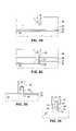
- FIG. 1there is shown a cross-sectional view of an NROM device 1 of the prior art.
- the device 1is made on a silicon substrate 2 with a first conductivity type, and with first and second regions 3 / 4 spaced apart from one another which are of a second conductivity type different from the first conductivity type of the silicon substrate 2 . Separating the first region 3 from the second region 4 is a channel region 5 .
- a first insulating layer 6such as silicon oxide or silicon dioxide is formed over the channel region 5 .
- a dielectric 7such as silicon nitride, is positioned over the silicon dioxide layer 6 .
- a second insulating layer 8such as another layer of silicon dioxide is positioned over the dielectric 7 .
- the first insulating layer 6 , the dielectric layer 7 and the second insulating layer 8are also known as an ONO layer 6 – 8 .
- a polysilicon gate 9is positioned on the second layer silicon dioxide 8 .
- the dielectric 7is spaced apart and is insulated from the channel region 5 via the first insulating layer 6 .
- the polysilicon gate 9is insulated and separated from the dielectric 7 by the second insulating layer of silicon dioxide 8 .
- the polysilicon gate 9is spaced apart and separated from the channel region 5 by the ONO layer 6 – 8 .
- the NROM device 1is a double density, nonvolatile storage cell, capable of storing 2 bits of information in the cell.
- the polysilicon layer 9serves as the gate and controls the flow of current between the first region 3 and the second region 4 through the channel region 5 .
- the polysilicon gate 9is raised to a high positive voltage.
- the first region 3is held at or near ground and the second region 4 is raised to a high positive voltage. Electrons from the first region 3 accelerate into the channel 5 towards the second region 4 and through hot channel electron injection mechanism are injected through the first oxide layer 6 and are trapped in the dielectric 7 near the region 10 of the dielectric layer 7 . Since the dielectric layer 7 , comprising of silicon nitride is a nonconductive material, the charges are trapped in the region 10 .
- the polysilicon layer 9is raised to a high positive voltage.
- the second region 4is held at or near ground and the first region 3 is raised to a high positive voltage. Electrons from the second region 4 accelerate in the channel 5 towards the first region 3 and through hot channel electron injection mechanism are injected through the first silicon dioxide layer 6 and are trapped in the region 11 of the dielectric layer 7 . Again, since the silicon nitride layer 7 is nonconductive, the charges are trapped in the region 11 .
- the first region 3is held near ground.
- a positive bias voltageis applied to the polysilicon layer 9 .
- the voltage appliedis such that if the region 11 does not contain trapped charges (i.e. is not programmed), it will cause the channel region 5 underneath it to be conductive. However, if the region 11 has trapped charges (i.e. is programmed), the channel region 5 underneath will not be conductive (not be turned on).
- a positive voltageis also applied to the second region 4 .
- the voltage applied to the second region 4is such that it causes a depletion region of the second region 4 to expand and encroach the channel region 5 so that it extends beyond the region 10 .
- the state of whether region 10 is programmed or notis irrelevant in reading region 11 of the memory cell. Therefore, under that condition, the state of conduction of the channel 5 between the first region 3 and the second region 4 is dependent solely on the state of charge stored or trapped in the region 11 .
- the voltages appliedare simply reversed.
- the second region 4is held near ground.
- a positive bias voltageis applied to the polysilicon layer 9 .
- the voltage appliedis such that if region 10 is not programmed, it will cause the channel region 5 underneath it to be conductive. However, if region 10 is programmed, channel region 5 underneath will not be conductive (not be turned on).
- a positive voltageis also applied to the first region 3 .
- the voltage applied to first region 3is such that it causes the depletion region of the first region 3 to expand and encroach into the channel region 5 beyond region 11 so that the state of charge stored or trapped in region 11 is irrelevant in reading region 10 of the memory cell.
- the substrate 2 , the first region 3 , and the second region 4may be connected to a high positive voltage thereby causing electrons from the trapped regions 10 and 11 to tunnel via Fowler/Nordheim tunneling into the substrate 2 .
- the problem with the NROM cell 1 of the prior artis that the channel 5 is on the planar surface of the silicon substrate 2 , and channel region 5 needs to be sufficiently large so that the two trapped regions 10 and 11 are sufficiently separated. This becomes a problem as the cell 1 is scaled to smaller sizes, especially since the thickness of the ONO layers 6 – 8 cannot be scaled.
- FIG. 2illustrates another prior art design of a NROM device which stores charges in a dielectric layer, with a split gate memory cell configuration.
- oxide and nitride layers 6 – 7along with a memory gate electrode 8 , are disposed over only a first section of the channel region 5 .
- the polysilicon gate 9has a lower portion that is disposed over and insulated from a second section of the channel region 5 (via insulation material 12 ), and a second portion that extends up and over oxide 6 , nitride 7 and memory gate 8 .
- Electrical contacts 13 and 14are formed to make electrical contact with first and second regions 3 / 4 .
- the effective channel lengthneeds to be long enough to tolerate different lithographic steps used to form the separate poly gate 9 and oxide 6 /nitride 7 /gate 8 .
- the width of the oxide/nitride/gate 6 / 7 / 8is at least one lithographic feature length long, which is unnecessarily long given that the trapped charges are immobile within the dielectric material.
- the present inventionsolves the aforementioned problems by forming the memory gates with isolated nitride storage nodes defined by spacer dimensions smaller than a lithographic limitation.
- the present inventionis a method of forming a memory device on a substrate of a first conductivity type, including forming an electron trapping dielectric material over the substrate, forming a first conductive material over the dielectric material, forming a spacer of material over the first conductive material, removing portions of the dielectric material and the first conductive material to form segments of the dielectric and the first conductive materials disposed underneath the spacer of material, forming first and second spaced-apart regions in the substrate having a second conductivity type different from the first conductivity type wherein a channel region with first and second portions is defined in the substrate between the first and second regions and wherein the segments of the dielectric and first conductive materials are disposed over the channel region first portion for controlling a conductivity thereof, and forming a second conductive material over and insulated from the channel region second portion for controlling a conductivity thereof.
- the present inventionis also a method for forming a memory device on a substrate of a first conductivity type that includes forming a first layer of an electron trapping dielectric material over the substrate, forming a second layer of a conductive material over the first layer, forming a third layer of a material over the second layer, forming a trench in the third layer, forming spacers of material along sidewalls of the trench, forming a first region in the substrate this is disposed under the trench and has a second conductivity type different from the first conductivity type, removing portions of the third layer adjacent the trench, removing portions of the first and second layers to form segments of the first and second layers that are each disposed under one of the spacers of material, forming a fourth layer of a conductive material over and insulated from the substrate, forming a pair of second regions in the substrate having the second conductivity type, wherein a pair of channel regions are each defined in the substrate between the first region and one of the pair of second regions, and wherein each channel region includes a first
- a method of forming a memory device on a substrate of a first conductivity typeincludes forming pairs of memory cells on the substrate, forming a plurality of first regions in the substrate, and forming a layer of second conductive material. Forming each of the memory cell pairs includes forming an electron trapping dielectric material over the substrate, forming a first conductive material over the dielectric material, forming a pair of spacers of material over the first conductive material, and removing portions of the dielectric material and the first conductive material to form segments of the dielectric and the first conductive materials each disposed underneath one of the spacers of material.
- the forming of the first regionsincludes forming a plurality of first regions in the substrate where each is disposed under one of the memory cell pairs and has a second conductivity type different from the first conductivity type, wherein a plurality of channel regions are defined in the substrate each extending between adjacent pairs of the first regions, and wherein each of the channel regions have first and second portions.
- the forming of the layer of second conductive materialincludes forming a layer of second conductive material that extends over the pairs of memory cells and that includes portions each of which extend over and are insulated from one of the channel region second portions for controlling a conductivity thereof. Each of the segments of the dielectric and first conductive materials are disposed over one of the channel region first portions for controlling a conductivity thereof.
- a memory devicein yet one more aspect of the present invention, includes pairs of memory cells formed on a substrate of a first conductivity type, a plurality of channel regions and a layer of second conductive material.
- Each of the memory cell pairsincludes a pair of electron trapping dielectric material segments disposed over the substrate, a pair of first conductive material segments disposed over the dielectric material segments, a pair of spacers of material disposed over the first conductive material segments, and a first region formed in the substrate under the memory cell pair and having a second conductivity type different from the first conductivity type.
- the plurality of channel regionsare defined in the substrate each extending between adjacent pairs of the first regions, wherein each of the channel regions have first and second portions, and wherein each of the segments of the dielectric and first conductive materials are disposed over one of the channel region first portions for controlling a conductivity thereof.
- the layer of second conductive materialextends over the pairs of memory cells and includes portions each of which extend over and are insulated from one of the channel region second portions for controlling a conductivity thereof.
- FIG. 1is a cross-sectional side view of a conventional memory cell.
- FIG. 2is a cross-sectional side view of another conventional memory cell.
- FIG. 3A to 3Hare cross-sectional side views of one of the active regions showing in sequence the process for forming a non volatile memory array of electron trapping memory cells of the present invention.
- FIG. 4is a cross-sectional side view of an alternative embodiment of the electron trapping memory cells of the present invention.
- FIG. 5is an enlarged cross-sectional side view of the alternative embodiment of the electron trapping memory cells of the present invention.
- the present inventionis a method of forming an NROM device in a self aligned manner.
- the dimensions of the memory cell componentscan be more easily and reliably scaled down to smaller dimensions.
- FIGS. 3A to 3Hillustrate the formation of the memory cells of the present invention. These figures illustrate cross section views of one portion of one of the active regions, which are formed in-between isolation regions. The formation of isolation regions (via LOCOS, STI, etc.) interleaved among active regions is well known in the art and not further discussed herein. The following figures illustrate the formation of a single pair of memory cells, wherein the process in fact produces many such memory cell pairs in each of the active regions.
- a layer of insulation materialis formed on the substrate 10 by well known techniques such as oxidation or deposition (e.g. chemical vapor deposition or CVD), forming a layer of silicon dioxide (oxide) preferably 2–8 nm thick.
- a layer of dielectric material 24such as silicon nitride (nitride) is formed over the oxide layer 22 preferably by CVD (e.g. 3–12 nm thick).
- a layer of polysilicon 26(hereinafter “poly”) is deposited over the nitride layer 24 (e.g. 10–20 nm thick), by a well known process such as Low Pressure CVD or LPCVD.
- a sacrificial layer of material 28is formed over poly layer 26 , again preferably by CVD (e.g. 20–40 nm thick). It should be well understood that all of the parameters described herein depend upon the design rules and the process technology generation, and one skilled in the art would understand that the present invention is not limited to any specific process technology generation, nor to any specific value in any of the process parameters described herein. The resulting structure is shown in FIG. 3A .
- a trench 30is formed into the nitride layer 28 , preferably using a conventional photo-lithography process (e.g. form mask layer over portions of nitride 28 , and performing an anisotropic nitride etch to remove exposed portions of nitride 28 ).
- the width of trench 30can be as small as the smallest possible lithographic feature for the process used.
- Trench 30extends down to and exposes poly layer 26 .
- first spacers 32are formed along the sidewalls of the trench 30 .
- the formation of spacersis well known in the art, and includes depositing a material over the contour of a structure, followed by an anisotropic etch process (e.g.
- first spacers 32a thick layer of oxide is deposited over the structure, followed by an anisotropic oxide etch, which removes the deposited oxide except for first spacers 32 inside trenches 30 .
- the resulting structureis shown in FIG. 3B .
- Anisotropic poly, nitride and oxide etchesfollow, to remove exposed portions of poly layer 26 , nitride layer 24 and oxide layer 22 , for extending trench 30 down to and exposing substrate 20 .
- the lower portion of trench 30has a width less than that of the upper portion of the trench 30 ).
- Second spacers 34are next formed in the lower portion of trench 30 by oxide deposition and anisotropic etch, further narrowing the lower portion of trench 30 .
- the trench 30is then filled with a block of polysilicon 36 by depositing a thick poly layer over the structure, followed by a planarizing poly etch (e.g. CMP-Chemical Mechanical Polish) that uses nitride 28 as an etch stop.
- a planarizing poly etche.g. CMP-Chemical Mechanical Polish
- Suitable ion implantationis then made across the entire surface of the structure, where the ions form a first region (i.e. source region) 38 in the exposed portion of substrate 20 at the bottom of trench 30 . It should be noted that some or all of this ion implantation can occur before the formation of second spacers 34 , depending upon the desired width of the source region 38 .
- the resulting structureis shown in FIG. 3C .
- a protective oxide layer 40is next formed on the top exposed portion of poly block 36 .
- Oxide layer 40is preferably formed via thermal oxidation or by TEOS (tetra-ethyl-ortho-silicate) deposition.
- TEOStetra-ethyl-ortho-silicate
- a nitride etchfollows, which removes nitride layer 28 .
- An anisotropic poly etchis used to remove exposed portions of poly layer 26 , leaving only segments of poly layer 26 directly under first spacers 32 , as shown in FIG. 3D .
- Thermal oxidationis then used to form a layer of oxide 42 on the exposed (side) portions of poly layer 26 .
- Anisotropic nitride and oxide etchesare performed to remove exposed portions of nitride layer 24 and oxide layer 22 , leaving separate segments of these layers under spacers 32 , where the width of these segments are defined by the width of the spacers 32 .
- the resulting structureis shown in FIG. 3E .
- a thin insulation layer 44is next formed on the exposed portions of substrate 20 , preferably made of oxide formed by thermal oxidation.
- a poly layer 46is then formed over the structure, as illustrated in FIG. 3F .
- Nitride spacers 48are then formed along the vertical portions of poly layer 44 by nitride deposition and anisotropic etch. An anisotropic poly etch is then used to remove those portions of poly layer 44 not protected by nitride spacers 48 .
- Suitable ion implantationis used (with any appropriate blocking masks) to form second regions (i.e. drain regions) 44 in the exposed portions of the substrate 20 .
- the resulting structureis shown in FIG. 3G .
- Additional nitride spacers 52are formed with a nitride deposition and etch process, for sealing and protecting the exposed ends of the poly layer 46 .
- Passivation or other insulating materialsuch as BPSG 54 , is used to cover the structure.
- a masking stepis performed to define etching areas over the second (drain) regions 50 .
- the BPSG 54is selectively etched in the etching areas to create contact openings that extend down to second (drain) regions 50 .
- the contact openingsare then filled with conductor metal contacts 56 by metal deposition and planarizing etch-back.
- the final memory cell structureis shown in FIG. 3H . It should be noted that other processing steps can be intermixed in the above process for forming other memory devices, well implant areas and/or peripheral devices on the same substrate.
- the process of the present inventionforms pairs of memory cells 60 that mirror each other, with first and second regions 38 / 50 forming the source and drain for each cell (those skilled in the art know that source and drain can be switched during operation).
- Each pair of memory cellsshares a single source region 38 .
- the channel region 58 for each cellis the portion of the substrate that is in-between the source and drain 38 / 50 .
- poly layer 46constitutes the control gate
- poly layer segment 26constitutes the memory gate
- nitride layer segment 24serves as the charge trapping dielectric material.
- Control gate 46is disposed over a first portion of the channel region 58 (insulated therefrom by oxide 44 ), and charge trapping dielectric 24 is disposed over a second portion of the channel region 58 .
- Memory gate 26is disposed over charge trapping dielectric 24 .
- a common contact 62 linecan be formed to connect all the metal contacts 56 in the active region together.
- Poly block 36 , memory gates 26 and control gates 46preferably extend through all the isolation and active regions forming lines that connect together like components from other pairs of memory cells in other active regions. Thus, any given memory cell in the array can be selected by the appropriate combination of the contact line ( 62 ), memory gate line ( 26 ), source line ( 36 ) and control gate line ( 46 ).
- the memory gate 26is raised to a positive voltage (e.g. 4–10V)
- the control gate 46is raised to a positive voltage (e.g. 1–3V)
- the drain region 50is held at or near ground potential
- the source region 38is raised to a positive voltage (e.g. 4–8V). Electrons from the drain region 50 accelerate into the channel region 58 towards the source region 38 , and through hot channel electron injection are injected through the oxide layer 22 and are trapped in charge trapping dielectric 24 .
- the drain region 50is held near ground potential. Voltages are applied to memory gate 26 (e.g. ⁇ 5 to +5V), control gate 46 (e.g. 2–4V) and source groin 38 (e.g. 1–3V). The positive voltage on the control gate 46 will turn on (make conductive) that portion of the channel region 58 under the control gate 46 .
- the voltage applied to the memory gate 26is such that if charge trapping dielectric 24 does not contain trapped electron charges (i.e. is not programmed), it will cause the portion of channel region 58 underneath it to be turned on (i.e. conductive) as well.
- channel conductivitymay be detected by switching the above described drain and source potentials, so that current flows is in the opposite direction.
- the substrate 20 and source 38may be connected to a high positive voltage thereby injecting holes from the substrate into the charge trapping dielectric 24 to neutralize the trapped electrons.
- either the memory gate 26 or control gate 46can be raised to a high voltage to inject the holes into the charge trapping dielectric 24 .
- the design and process of the present inventionhas many advantages.
- the memory cellsare made using a single photo-lithographic step. This means that the memory cell components are all self aligned to each other, thus allowing better scaling to small geometries and eliminating alignment tolerance issues for multiple photo-lithography steps.
- the dimensions of key memory cell componentsare more controllable and can be smaller than the single feature resolution of the photo-lithographic step.
- spacers 32are used to define the width of memory gate 26 and the charge trapping dielectric 24 .
- the deposition thickness of poly 46 and spacers 48are used to define the width of control gate 46 over channel region 58 .
- the overall memory cell sizeis reduced, and component sizes can be better and more uniformly controlled.
- Improved hot electron injectionis achieved by having the electrons pass the gap between the control gate 46 and the memory gate 26 , which accelerates the electrons even faster for better injection efficiency and faster speed.
- FIG. 4illustrates an alternate embodiment of the present invention, which is a bidirectional version of the self aligned memory cell described above.
- the present embodimentincludes the same structure shown in FIG. 3F , except that the poly layer 46 is selectively removed from the isolation regions separating the active regions (preferably using a masking/etch process), leaving strips of poly 46 each extending along the length of one of the active regions.
- This configurationoperates in a similar manner to that described above, except that the source (first) region 38 from one pair of memory cells is operationally used as the drain (second) region for the adjacent pairs of memory cells, and vice versa.
- FIG. 5shows two adjacent memory cells (left hand memory cell 60 L and right hand memory cell 60 R) from adjacent pairs of memory cells 60 .
- the memory gate 26 Ris raised to a positive voltage (e.g. 4–8V)
- the control gate 46is raised to a positive voltage (e.g. 1–3V)
- the source region 38 Lis held at or near ground potential
- the source region 38 Ris raised to a positive voltage (e.g. 2–5V).
- Electrons from the source region 38 Laccelerate into the channel region 58 towards the source region 38 R and through hot channel electron injection are injected through the oxide layer 22 and are trapped in the charge trapping dielectric 24 R.
- the left and right voltages aboveare reversed.
- the source region 38 Ris held near ground. Positive voltages are applied to memory gate 26 R (e.g. ⁇ 3 to 0V) and to control gate 46 (e.g. 1–4V). A positive voltage is applied to the source region 38 L such that it causes a depletion region of the source region 38 L to expand and encroach the channel region 58 so that it extends beyond charge trapping dielectric 24 L. A positive voltage (e.g. 0–3V) may be applied to the memory gate 26 L to enhance the depletion region formation around region 38 L. Thus, the state of whether charge trapping dielectric 24 L is programmed or not is irrelevant in reading memory cell 60 R.
- the positive voltage on the control gate 46will turn on (make conductive) that portion of the channel region 58 under the control gate 46 .
- the voltage applied to the memory gate 26 Ris such that if charge trapping dielectric 24 R does not contain trapped electron charges (i.e. is not programmed), it will cause the portion of channel region 58 underneath it to be turned on (i.e. conductive) as well. With both portions of the channel region conductive, electrical current will flow across the channel region 58 , indicating an unprogrammed state (e.g. a “0” state). However, if charge trapping dielectric 24 R does contain trapped electron charges (i.e. is programmed), the portion of channel region 58 underneath will not be turned on (i.e. not conductive). With part of the channel region turned off, little or no electrical current will flow across the channel region, indicating a programmed state (e.g. a “1” state). To read the left hand memory cell 60 L, the left and right voltages above are reversed.
- the substrate 20 and source(s) 38 R and/or 38 Lmay be connected to a high positive voltage thereby injecting holes from the substrate into the charge trapping dielectrics 24 R and/or 24 L to neutralize the trapped electrons.
- either the memory gates 26 R and 26 L or control gate 46can be raised to a high voltage to inject the holes into the charge trapping dielectrics 24 R and/or 24 L.
- the terms “over” and “on” and “under” inclusivelyinclude “directly on” or “directly under” (no intermediate materials, elements or space disposed therebetween) and “indirectly on” or “indirectly under” (intermediate materials, elements or space disposed therebetween).
- the term “adjacent”includes “directly adjacent” (no intermediate materials, elements or space disposed therebetween) and “indirectly adjacent” (intermediate materials, elements or space disposed therebetween).
- forming an element “over a substrate”can include forming the element directly on the substrate with no intermediate materials/elements therebetween, as well as forming the element indirectly on the substrate with one or more intermediate materials/elements therebetween.
Landscapes
- Engineering & Computer Science (AREA)
- Physics & Mathematics (AREA)
- Condensed Matter Physics & Semiconductors (AREA)
- General Physics & Mathematics (AREA)
- Manufacturing & Machinery (AREA)
- Computer Hardware Design (AREA)
- Microelectronics & Electronic Packaging (AREA)
- Power Engineering (AREA)
- Non-Volatile Memory (AREA)
- Semiconductor Memories (AREA)
- Bipolar Transistors (AREA)
Abstract
Description
Claims (4)
Priority Applications (5)
| Application Number | Priority Date | Filing Date | Title |
|---|---|---|---|
| US10/962,008US7119396B2 (en) | 2004-10-08 | 2004-10-08 | NROM device |
| TW094131508ATWI358090B (en) | 2004-10-08 | 2005-09-13 | Nrom device and method of making same |
| JP2005322821AJP5348824B2 (en) | 2004-10-08 | 2005-10-07 | NROM device and manufacturing method thereof |
| KR1020050094338AKR101138214B1 (en) | 2004-10-08 | 2005-10-07 | NROM device and method of making same |
| CNB2005101084151ACN100501976C (en) | 2004-10-08 | 2005-10-08 | NROM device and its manufacturing method |
Applications Claiming Priority (1)
| Application Number | Priority Date | Filing Date | Title |
|---|---|---|---|
| US10/962,008US7119396B2 (en) | 2004-10-08 | 2004-10-08 | NROM device |
Publications (2)
| Publication Number | Publication Date |
|---|---|
| US20060079053A1 US20060079053A1 (en) | 2006-04-13 |
| US7119396B2true US7119396B2 (en) | 2006-10-10 |
Family
ID=36145892
Family Applications (1)
| Application Number | Title | Priority Date | Filing Date |
|---|---|---|---|
| US10/962,008Expired - LifetimeUS7119396B2 (en) | 2004-10-08 | 2004-10-08 | NROM device |
Country Status (5)
| Country | Link |
|---|---|
| US (1) | US7119396B2 (en) |
| JP (1) | JP5348824B2 (en) |
| KR (1) | KR101138214B1 (en) |
| CN (1) | CN100501976C (en) |
| TW (1) | TWI358090B (en) |
Cited By (4)
| Publication number | Priority date | Publication date | Assignee | Title |
|---|---|---|---|---|
| US20100001338A1 (en)* | 2008-07-03 | 2010-01-07 | Nec Electronics Corporation | Non-volatile semiconductor memory device, and manufacture method for non-volatile semiconductor memory device |
| US20170098654A1 (en)* | 2015-10-01 | 2017-04-06 | Silicon Storage Technology, Inc. | Non-volatile split gate memory cells with integrated high k metal gate, and method of making same |
| US20170103989A1 (en)* | 2015-10-07 | 2017-04-13 | Silicon Storage Technology, Inc. | Method Of Making Embedded Memory Device With Silicon-On-Insulator Substrate |
| US10714634B2 (en) | 2017-12-05 | 2020-07-14 | Silicon Storage Technology, Inc. | Non-volatile split gate memory cells with integrated high K metal control gates and method of making same |
Families Citing this family (6)
| Publication number | Priority date | Publication date | Assignee | Title |
|---|---|---|---|---|
| US8803217B2 (en)* | 2007-03-13 | 2014-08-12 | Freescale Semiconductor, Inc. | Process of forming an electronic device including a control gate electrode, a semiconductor layer, and a select gate electrode |
| US7916544B2 (en)* | 2008-01-25 | 2011-03-29 | Micron Technology, Inc. | Random telegraph signal noise reduction scheme for semiconductor memories |
| CN101777561B (en)* | 2010-01-12 | 2013-05-01 | 上海宏力半导体制造有限公司 | Split-gate type nonvolatile storage and production method thereof |
| US9484261B2 (en)* | 2013-07-05 | 2016-11-01 | Silicon Storage Technology, Inc. | Formation of self-aligned source for split-gate non-volatile memory cell |
| US9472645B1 (en)* | 2015-06-08 | 2016-10-18 | Taiwan Semiconductor Manufacturing Co., Ltd. | Dual control gate spacer structure for embedded flash memory |
| US10797647B1 (en)* | 2019-08-05 | 2020-10-06 | GM Global Technology Operations LLC | Receiver apparatus |
Citations (7)
| Publication number | Priority date | Publication date | Assignee | Title |
|---|---|---|---|---|
| US5768192A (en) | 1996-07-23 | 1998-06-16 | Saifun Semiconductors, Ltd. | Non-volatile semiconductor memory cell utilizing asymmetrical charge trapping |
| US6011725A (en) | 1997-08-01 | 2000-01-04 | Saifun Semiconductors, Ltd. | Two bit non-volatile electrically erasable and programmable semiconductor memory cell utilizing asymmetrical charge trapping |
| US6486028B1 (en) | 2001-11-20 | 2002-11-26 | Macronix International Co., Ltd. | Method of fabricating a nitride read-only-memory cell vertical structure |
| US6559500B2 (en)* | 2001-03-29 | 2003-05-06 | Fujitsu Limited | Non-volatile semiconductor memory and its driving method |
| US20030235076A1 (en) | 2002-06-21 | 2003-12-25 | Micron Technology, Inc. | Multistate NROM having a storage density much greater than 1 Bit per 1F2 |
| US6773994B2 (en) | 2001-12-26 | 2004-08-10 | Agere Systems Inc. | CMOS vertical replacement gate (VRG) transistors |
| US6853587B2 (en)* | 2002-06-21 | 2005-02-08 | Micron Technology, Inc. | Vertical NROM having a storage density of 1 bit per 1F2 |
Family Cites Families (10)
| Publication number | Priority date | Publication date | Assignee | Title |
|---|---|---|---|---|
| US6255166B1 (en)* | 1999-08-05 | 2001-07-03 | Aalo Lsi Design & Device Technology, Inc. | Nonvolatile memory cell, method of programming the same and nonvolatile memory array |
| US6329685B1 (en)* | 1999-09-22 | 2001-12-11 | Silicon Storage Technology, Inc. | Self aligned method of forming a semiconductor memory array of floating gate memory cells and a memory array made thereby |
| US6525371B2 (en)* | 1999-09-22 | 2003-02-25 | International Business Machines Corporation | Self-aligned non-volatile random access memory cell and process to make the same |
| JP2001357681A (en)* | 2000-06-12 | 2001-12-26 | Sony Corp | Semiconductor storage device and its driving method |
| TW503528B (en)* | 2000-07-12 | 2002-09-21 | Koninkl Philips Electronics Nv | Semiconductor device |
| KR100437470B1 (en)* | 2001-01-31 | 2004-06-23 | 삼성전자주식회사 | Semiconductor device having a flash memory cell and fabrication method thereof |
| JP3983105B2 (en)* | 2002-05-29 | 2007-09-26 | Necエレクトロニクス株式会社 | Method for manufacturing nonvolatile semiconductor memory device |
| JP2004152924A (en)* | 2002-10-30 | 2004-05-27 | Renesas Technology Corp | Semiconductor storage element and semiconductor device |
| KR100480645B1 (en)* | 2003-04-01 | 2005-03-31 | 삼성전자주식회사 | Method for manufacturing SONOS memory device with twin-ONO by reverse self-aligning process |
| KR100525448B1 (en)* | 2004-04-30 | 2005-11-02 | 동부아남반도체 주식회사 | Method for fabricating of flash memory device |
- 2004
- 2004-10-08USUS10/962,008patent/US7119396B2/ennot_activeExpired - Lifetime
- 2005
- 2005-09-13TWTW094131508Apatent/TWI358090B/enactive
- 2005-10-07JPJP2005322821Apatent/JP5348824B2/ennot_activeExpired - Fee Related
- 2005-10-07KRKR1020050094338Apatent/KR101138214B1/ennot_activeExpired - Lifetime
- 2005-10-08CNCNB2005101084151Apatent/CN100501976C/ennot_activeExpired - Fee Related
Patent Citations (7)
| Publication number | Priority date | Publication date | Assignee | Title |
|---|---|---|---|---|
| US5768192A (en) | 1996-07-23 | 1998-06-16 | Saifun Semiconductors, Ltd. | Non-volatile semiconductor memory cell utilizing asymmetrical charge trapping |
| US6011725A (en) | 1997-08-01 | 2000-01-04 | Saifun Semiconductors, Ltd. | Two bit non-volatile electrically erasable and programmable semiconductor memory cell utilizing asymmetrical charge trapping |
| US6559500B2 (en)* | 2001-03-29 | 2003-05-06 | Fujitsu Limited | Non-volatile semiconductor memory and its driving method |
| US6486028B1 (en) | 2001-11-20 | 2002-11-26 | Macronix International Co., Ltd. | Method of fabricating a nitride read-only-memory cell vertical structure |
| US6773994B2 (en) | 2001-12-26 | 2004-08-10 | Agere Systems Inc. | CMOS vertical replacement gate (VRG) transistors |
| US20030235076A1 (en) | 2002-06-21 | 2003-12-25 | Micron Technology, Inc. | Multistate NROM having a storage density much greater than 1 Bit per 1F2 |
| US6853587B2 (en)* | 2002-06-21 | 2005-02-08 | Micron Technology, Inc. | Vertical NROM having a storage density of 1 bit per 1F2 |
Cited By (6)
| Publication number | Priority date | Publication date | Assignee | Title |
|---|---|---|---|---|
| US20100001338A1 (en)* | 2008-07-03 | 2010-01-07 | Nec Electronics Corporation | Non-volatile semiconductor memory device, and manufacture method for non-volatile semiconductor memory device |
| US20170098654A1 (en)* | 2015-10-01 | 2017-04-06 | Silicon Storage Technology, Inc. | Non-volatile split gate memory cells with integrated high k metal gate, and method of making same |
| US9634019B1 (en)* | 2015-10-01 | 2017-04-25 | Silicon Storage Technology, Inc. | Non-volatile split gate memory cells with integrated high K metal gate, and method of making same |
| US20170103989A1 (en)* | 2015-10-07 | 2017-04-13 | Silicon Storage Technology, Inc. | Method Of Making Embedded Memory Device With Silicon-On-Insulator Substrate |
| US9634020B1 (en)* | 2015-10-07 | 2017-04-25 | Silicon Storage Technology, Inc. | Method of making embedded memory device with silicon-on-insulator substrate |
| US10714634B2 (en) | 2017-12-05 | 2020-07-14 | Silicon Storage Technology, Inc. | Non-volatile split gate memory cells with integrated high K metal control gates and method of making same |
Also Published As
| Publication number | Publication date |
|---|---|
| TWI358090B (en) | 2012-02-11 |
| CN1835210A (en) | 2006-09-20 |
| KR101138214B1 (en) | 2012-04-24 |
| US20060079053A1 (en) | 2006-04-13 |
| TW200618124A (en) | 2006-06-01 |
| JP5348824B2 (en) | 2013-11-20 |
| CN100501976C (en) | 2009-06-17 |
| KR20060052105A (en) | 2006-05-19 |
| JP2006114921A (en) | 2006-04-27 |
Similar Documents
| Publication | Publication Date | Title |
|---|---|---|
| KR100472163B1 (en) | Self-aligned method of forming a semiconductor memory array of floating gate memory cells with buried source line and floating gate, and a memory array made thereby | |
| US7205198B2 (en) | Method of making a bi-directional read/program non-volatile floating gate memory cell | |
| US7315056B2 (en) | Semiconductor memory array of floating gate memory cells with program/erase and select gates | |
| US6764905B2 (en) | Method of manufacturing a scalable flash EEPROM memory cell with floating gate spacer wrapped by control gate | |
| US6917069B2 (en) | Semiconductor memory array of floating gate memory cells with buried bit-line and vertical word line transistor | |
| CN100440514C (en) | Nonvolatile floating gate memory cell, its array, and its forming method | |
| US9461182B2 (en) | Memory cell | |
| WO2017189179A1 (en) | Split-gate, twin-bit non-volatile memory cell | |
| US7119396B2 (en) | NROM device | |
| US6822287B1 (en) | Array of integrated circuit units with strapping lines to prevent punch through | |
| US6936883B2 (en) | Bi-directional read/program non-volatile floating gate memory cell and array thereof, and method of formation | |
| JP2005142354A (en) | Nonvolatile semiconductor memory device, driving method thereof, and manufacturing method thereof | |
| US6972230B1 (en) | Method for fabricating a floating gate memory device | |
| US11404545B2 (en) | Method of forming split-gate flash memory cell with spacer defined floating gate and discretely formed polysilicon gates | |
| JP4662680B2 (en) | Self-alignment method for forming a semiconductor memory array of floating gate memory cells with buried bit lines and raised source lines and memory array manufactured by the method | |
| US7008846B2 (en) | Non-volatile floating gate memory cell with floating gates formed as spacers, and an array thereof, and a method of manufacturing | |
| US7358559B2 (en) | Bi-directional read/program non-volatile floating gate memory array, and method of formation | |
| JP2005260235A (en) | Embedded bit line type nonvolatile floating gate memory cell having independently controllable control gate in trench, array thereof, and manufacturing method thereof |
Legal Events
| Date | Code | Title | Description |
|---|---|---|---|
| AS | Assignment | Owner name:SILICON STORAGE TECHNOLOGY, INC., CALIFORNIA Free format text:ASSIGNMENT OF ASSIGNORS INTEREST;ASSIGNORS:CHEN, BOMY;LEE, DANA;HU, YAW WEN;AND OTHERS;REEL/FRAME:015656/0216;SIGNING DATES FROM 20050112 TO 20050117 | |
| STCF | Information on status: patent grant | Free format text:PATENTED CASE | |
| FPAY | Fee payment | Year of fee payment:4 | |
| FPAY | Fee payment | Year of fee payment:8 | |
| AS | Assignment | Owner name:JPMORGAN CHASE BANK, N.A., AS ADMINISTRATIVE AGENT, ILLINOIS Free format text:SECURITY INTEREST;ASSIGNOR:SILICON STORAGE TECHNOLOGY, INC.;REEL/FRAME:041675/0316 Effective date:20170208 Owner name:JPMORGAN CHASE BANK, N.A., AS ADMINISTRATIVE AGENT Free format text:SECURITY INTEREST;ASSIGNOR:SILICON STORAGE TECHNOLOGY, INC.;REEL/FRAME:041675/0316 Effective date:20170208 | |
| MAFP | Maintenance fee payment | Free format text:PAYMENT OF MAINTENANCE FEE, 12TH YEAR, LARGE ENTITY (ORIGINAL EVENT CODE: M1553) Year of fee payment:12 | |
| AS | Assignment | Owner name:JPMORGAN CHASE BANK, N.A., AS ADMINISTRATIVE AGENT, ILLINOIS Free format text:SECURITY INTEREST;ASSIGNORS:MICROCHIP TECHNOLOGY INCORPORATED;SILICON STORAGE TECHNOLOGY, INC.;ATMEL CORPORATION;AND OTHERS;REEL/FRAME:046426/0001 Effective date:20180529 Owner name:JPMORGAN CHASE BANK, N.A., AS ADMINISTRATIVE AGENT Free format text:SECURITY INTEREST;ASSIGNORS:MICROCHIP TECHNOLOGY INCORPORATED;SILICON STORAGE TECHNOLOGY, INC.;ATMEL CORPORATION;AND OTHERS;REEL/FRAME:046426/0001 Effective date:20180529 | |
| AS | Assignment | Owner name:WELLS FARGO BANK, NATIONAL ASSOCIATION, AS NOTES COLLATERAL AGENT, CALIFORNIA Free format text:SECURITY INTEREST;ASSIGNORS:MICROCHIP TECHNOLOGY INCORPORATED;SILICON STORAGE TECHNOLOGY, INC.;ATMEL CORPORATION;AND OTHERS;REEL/FRAME:047103/0206 Effective date:20180914 Owner name:WELLS FARGO BANK, NATIONAL ASSOCIATION, AS NOTES C Free format text:SECURITY INTEREST;ASSIGNORS:MICROCHIP TECHNOLOGY INCORPORATED;SILICON STORAGE TECHNOLOGY, INC.;ATMEL CORPORATION;AND OTHERS;REEL/FRAME:047103/0206 Effective date:20180914 | |
| AS | Assignment | Owner name:JPMORGAN CHASE BANK, N.A., AS ADMINISTRATIVE AGENT, DELAWARE Free format text:SECURITY INTEREST;ASSIGNORS:MICROCHIP TECHNOLOGY INC.;SILICON STORAGE TECHNOLOGY, INC.;ATMEL CORPORATION;AND OTHERS;REEL/FRAME:053311/0305 Effective date:20200327 | |
| AS | Assignment | Owner name:MICROSEMI CORPORATION, CALIFORNIA Free format text:RELEASE BY SECURED PARTY;ASSIGNOR:JPMORGAN CHASE BANK, N.A, AS ADMINISTRATIVE AGENT;REEL/FRAME:053466/0011 Effective date:20200529 Owner name:ATMEL CORPORATION, ARIZONA Free format text:RELEASE BY SECURED PARTY;ASSIGNOR:JPMORGAN CHASE BANK, N.A, AS ADMINISTRATIVE AGENT;REEL/FRAME:053466/0011 Effective date:20200529 Owner name:SILICON STORAGE TECHNOLOGY, INC., ARIZONA Free format text:RELEASE BY SECURED PARTY;ASSIGNOR:JPMORGAN CHASE BANK, N.A, AS ADMINISTRATIVE AGENT;REEL/FRAME:053466/0011 Effective date:20200529 Owner name:MICROSEMI STORAGE SOLUTIONS, INC., ARIZONA Free format text:RELEASE BY SECURED PARTY;ASSIGNOR:JPMORGAN CHASE BANK, N.A, AS ADMINISTRATIVE AGENT;REEL/FRAME:053466/0011 Effective date:20200529 Owner name:MICROCHIP TECHNOLOGY INC., ARIZONA Free format text:RELEASE BY SECURED PARTY;ASSIGNOR:JPMORGAN CHASE BANK, N.A, AS ADMINISTRATIVE AGENT;REEL/FRAME:053466/0011 Effective date:20200529 | |
| AS | Assignment | Owner name:WELLS FARGO BANK, NATIONAL ASSOCIATION, MINNESOTA Free format text:SECURITY INTEREST;ASSIGNORS:MICROCHIP TECHNOLOGY INC.;SILICON STORAGE TECHNOLOGY, INC.;ATMEL CORPORATION;AND OTHERS;REEL/FRAME:053468/0705 Effective date:20200529 | |
| AS | Assignment | Owner name:WELLS FARGO BANK, NATIONAL ASSOCIATION, AS COLLATERAL AGENT, MINNESOTA Free format text:SECURITY INTEREST;ASSIGNORS:MICROCHIP TECHNOLOGY INCORPORATED;SILICON STORAGE TECHNOLOGY, INC.;ATMEL CORPORATION;AND OTHERS;REEL/FRAME:055671/0612 Effective date:20201217 | |
| AS | Assignment | Owner name:WELLS FARGO BANK, NATIONAL ASSOCIATION, AS NOTES COLLATERAL AGENT, MINNESOTA Free format text:SECURITY INTEREST;ASSIGNORS:MICROCHIP TECHNOLOGY INCORPORATED;SILICON STORAGE TECHNOLOGY, INC.;ATMEL CORPORATION;AND OTHERS;REEL/FRAME:057935/0474 Effective date:20210528 | |
| AS | Assignment | Owner name:MICROSEMI STORAGE SOLUTIONS, INC., ARIZONA Free format text:RELEASE BY SECURED PARTY;ASSIGNOR:JPMORGAN CHASE BANK, N.A., AS ADMINISTRATIVE AGENT;REEL/FRAME:059333/0222 Effective date:20220218 Owner name:MICROSEMI CORPORATION, ARIZONA Free format text:RELEASE BY SECURED PARTY;ASSIGNOR:JPMORGAN CHASE BANK, N.A., AS ADMINISTRATIVE AGENT;REEL/FRAME:059333/0222 Effective date:20220218 Owner name:ATMEL CORPORATION, ARIZONA Free format text:RELEASE BY SECURED PARTY;ASSIGNOR:JPMORGAN CHASE BANK, N.A., AS ADMINISTRATIVE AGENT;REEL/FRAME:059333/0222 Effective date:20220218 Owner name:SILICON STORAGE TECHNOLOGY, INC., ARIZONA Free format text:RELEASE BY SECURED PARTY;ASSIGNOR:JPMORGAN CHASE BANK, N.A., AS ADMINISTRATIVE AGENT;REEL/FRAME:059333/0222 Effective date:20220218 Owner name:MICROCHIP TECHNOLOGY INCORPORATED, ARIZONA Free format text:RELEASE BY SECURED PARTY;ASSIGNOR:JPMORGAN CHASE BANK, N.A., AS ADMINISTRATIVE AGENT;REEL/FRAME:059333/0222 Effective date:20220218 | |
| AS | Assignment | Owner name:SILICON STORAGE TECHNOLOGY, INC., ARIZONA Free format text:RELEASE BY SECURED PARTY;ASSIGNOR:JPMORGAN CHASE BANK, N.A., AS ADMINISTRATIVE AGENT;REEL/FRAME:059687/0344 Effective date:20220218 | |
| AS | Assignment | Owner name:MICROSEMI STORAGE SOLUTIONS, INC., ARIZONA Free format text:RELEASE BY SECURED PARTY;ASSIGNOR:WELLS FARGO BANK, NATIONAL ASSOCIATION, AS NOTES COLLATERAL AGENT;REEL/FRAME:059358/0001 Effective date:20220228 Owner name:MICROSEMI CORPORATION, ARIZONA Free format text:RELEASE BY SECURED PARTY;ASSIGNOR:WELLS FARGO BANK, NATIONAL ASSOCIATION, AS NOTES COLLATERAL AGENT;REEL/FRAME:059358/0001 Effective date:20220228 Owner name:ATMEL CORPORATION, ARIZONA Free format text:RELEASE BY SECURED PARTY;ASSIGNOR:WELLS FARGO BANK, NATIONAL ASSOCIATION, AS NOTES COLLATERAL AGENT;REEL/FRAME:059358/0001 Effective date:20220228 Owner name:SILICON STORAGE TECHNOLOGY, INC., ARIZONA Free format text:RELEASE BY SECURED PARTY;ASSIGNOR:WELLS FARGO BANK, NATIONAL ASSOCIATION, AS NOTES COLLATERAL AGENT;REEL/FRAME:059358/0001 Effective date:20220228 Owner name:MICROCHIP TECHNOLOGY INCORPORATED, ARIZONA Free format text:RELEASE BY SECURED PARTY;ASSIGNOR:WELLS FARGO BANK, NATIONAL ASSOCIATION, AS NOTES COLLATERAL AGENT;REEL/FRAME:059358/0001 Effective date:20220228 | |
| AS | Assignment | Owner name:MICROSEMI STORAGE SOLUTIONS, INC., ARIZONA Free format text:RELEASE BY SECURED PARTY;ASSIGNOR:WELLS FARGO BANK, NATIONAL ASSOCIATION, AS NOTES COLLATERAL AGENT;REEL/FRAME:059863/0400 Effective date:20220228 Owner name:MICROSEMI CORPORATION, ARIZONA Free format text:RELEASE BY SECURED PARTY;ASSIGNOR:WELLS FARGO BANK, NATIONAL ASSOCIATION, AS NOTES COLLATERAL AGENT;REEL/FRAME:059863/0400 Effective date:20220228 Owner name:ATMEL CORPORATION, ARIZONA Free format text:RELEASE BY SECURED PARTY;ASSIGNOR:WELLS FARGO BANK, NATIONAL ASSOCIATION, AS NOTES COLLATERAL AGENT;REEL/FRAME:059863/0400 Effective date:20220228 Owner name:SILICON STORAGE TECHNOLOGY, INC., ARIZONA Free format text:RELEASE BY SECURED PARTY;ASSIGNOR:WELLS FARGO BANK, NATIONAL ASSOCIATION, AS NOTES COLLATERAL AGENT;REEL/FRAME:059863/0400 Effective date:20220228 Owner name:MICROCHIP TECHNOLOGY INCORPORATED, ARIZONA Free format text:RELEASE BY SECURED PARTY;ASSIGNOR:WELLS FARGO BANK, NATIONAL ASSOCIATION, AS NOTES COLLATERAL AGENT;REEL/FRAME:059863/0400 Effective date:20220228 | |
| AS | Assignment | Owner name:MICROSEMI STORAGE SOLUTIONS, INC., ARIZONA Free format text:RELEASE BY SECURED PARTY;ASSIGNOR:WELLS FARGO BANK, NATIONAL ASSOCIATION, AS NOTES COLLATERAL AGENT;REEL/FRAME:059363/0001 Effective date:20220228 Owner name:MICROSEMI CORPORATION, ARIZONA Free format text:RELEASE BY SECURED PARTY;ASSIGNOR:WELLS FARGO BANK, NATIONAL ASSOCIATION, AS NOTES COLLATERAL AGENT;REEL/FRAME:059363/0001 Effective date:20220228 Owner name:ATMEL CORPORATION, ARIZONA Free format text:RELEASE BY SECURED PARTY;ASSIGNOR:WELLS FARGO BANK, NATIONAL ASSOCIATION, AS NOTES COLLATERAL AGENT;REEL/FRAME:059363/0001 Effective date:20220228 Owner name:SILICON STORAGE TECHNOLOGY, INC., ARIZONA Free format text:RELEASE BY SECURED PARTY;ASSIGNOR:WELLS FARGO BANK, NATIONAL ASSOCIATION, AS NOTES COLLATERAL AGENT;REEL/FRAME:059363/0001 Effective date:20220228 Owner name:MICROCHIP TECHNOLOGY INCORPORATED, ARIZONA Free format text:RELEASE BY SECURED PARTY;ASSIGNOR:WELLS FARGO BANK, NATIONAL ASSOCIATION, AS NOTES COLLATERAL AGENT;REEL/FRAME:059363/0001 Effective date:20220228 | |
| AS | Assignment | Owner name:MICROSEMI STORAGE SOLUTIONS, INC., ARIZONA Free format text:RELEASE BY SECURED PARTY;ASSIGNOR:WELLS FARGO BANK, NATIONAL ASSOCIATION, AS NOTES COLLATERAL AGENT;REEL/FRAME:060894/0437 Effective date:20220228 Owner name:MICROSEMI CORPORATION, ARIZONA Free format text:RELEASE BY SECURED PARTY;ASSIGNOR:WELLS FARGO BANK, NATIONAL ASSOCIATION, AS NOTES COLLATERAL AGENT;REEL/FRAME:060894/0437 Effective date:20220228 Owner name:ATMEL CORPORATION, ARIZONA Free format text:RELEASE BY SECURED PARTY;ASSIGNOR:WELLS FARGO BANK, NATIONAL ASSOCIATION, AS NOTES COLLATERAL AGENT;REEL/FRAME:060894/0437 Effective date:20220228 Owner name:SILICON STORAGE TECHNOLOGY, INC., ARIZONA Free format text:RELEASE BY SECURED PARTY;ASSIGNOR:WELLS FARGO BANK, NATIONAL ASSOCIATION, AS NOTES COLLATERAL AGENT;REEL/FRAME:060894/0437 Effective date:20220228 Owner name:MICROCHIP TECHNOLOGY INCORPORATED, ARIZONA Free format text:RELEASE BY SECURED PARTY;ASSIGNOR:WELLS FARGO BANK, NATIONAL ASSOCIATION, AS NOTES COLLATERAL AGENT;REEL/FRAME:060894/0437 Effective date:20220228 |