US7117022B2 - CDMA base station system - Google Patents
CDMA base station systemDownload PDFInfo
- Publication number
- US7117022B2 US7117022B2US09/735,547US73554700AUS7117022B2US 7117022 B2US7117022 B2US 7117022B2US 73554700 AUS73554700 AUS 73554700AUS 7117022 B2US7117022 B2US 7117022B2
- Authority
- US
- United States
- Prior art keywords
- signal
- coupled
- output signal
- output
- receive
- Prior art date
- Legal status (The legal status is an assumption and is not a legal conclusion. Google has not performed a legal analysis and makes no representation as to the accuracy of the status listed.)
- Expired - Fee Related, expires
Links
Images


Classifications
- H—ELECTRICITY
- H04—ELECTRIC COMMUNICATION TECHNIQUE
- H04W—WIRELESS COMMUNICATION NETWORKS
- H04W88/00—Devices specially adapted for wireless communication networks, e.g. terminals, base stations or access point devices
- H04W88/08—Access point devices
- H—ELECTRICITY
- H04—ELECTRIC COMMUNICATION TECHNIQUE
- H04B—TRANSMISSION
- H04B17/00—Monitoring; Testing
- H04B17/30—Monitoring; Testing of propagation channels
- H04B17/309—Measuring or estimating channel quality parameters
- H04B17/318—Received signal strength
- H—ELECTRICITY
- H04—ELECTRIC COMMUNICATION TECHNIQUE
- H04B—TRANSMISSION
- H04B7/00—Radio transmission systems, i.e. using radiation field
- H04B7/14—Relay systems
- H04B7/15—Active relay systems
- H04B7/155—Ground-based stations
Definitions
- the present inventionrelates to a code division multiple access (CDMA) base station system, and more particularly to a CDMA base station system which reduces the deterioration of call quality.
- CDMAcode division multiple access
- FIG. 1is a block diagram illustrating the construction of a related art CDMA base station system.
- the related art CDMA base stationincludes a base station processor 101 for taking charge of an interface in a base station and controlling peripheral boards. It further includes an upper processor 102 for taking charge of an interface between the base station and an exchange (not illustrated). The upper processor 102 is communicatively coupled to base station processor 101 . Next, a channel card 103 is provided to modulate/demodulate signals transmitted/received from the base station.
- the CDMA base stationalso includes a transmitted frequency converter 104 to convert a transmitted frequency into an allocated use frequency band, and a transmitted power amplifier 106 to amplify the signal to transmit at a rated power of the base station.
- a transmitted frequency band filter 108is provided to allow only the allocated frequency band (i.e., the transmitted frequency band to be used) to pass through to the transmitting antenna 111 .
- the CDMA base stationnext includes a received frequency converter 105 , to convert a received frequency into a frequency band used in the base station.
- a receiving amplifier 107is coupled to the frequency converter 105 for amplifying a low-level signal from a terminal, and a received frequency band filter 109 is coupled to the receiving amplifier 107 , and allows only the allocated frequency band to pass through.
- a power level measuring device 110is provided to measure a power level of a final end (i.e., an output) of the base station.
- the operation of the related art CDMA base stationis typically divided into three functions: (1) base station transmission; (2) base station reception; and (3) output signal strength detection.
- the channel card 103which controls the transmitted/received signal modulation and demodulation, modulates the transmitted signal of the CDMA base station.
- the modulated signalthen passes through the transmitted frequency band filter 108 via the transmitted frequency converter 104 . This is done to convert the transmitted signal into the frequency to be actually used (i.e., allocated use frequency).
- the signalpasses through the transmitted power amplifier 106 to increase the transmission power to the rated power (i.e., the maximum power of the base station that can be transmitted within the range satisfying the characteristic of the base station).
- the signalis then outputted from transmitted power amplifier 106 and passes through the transmitted frequency band filter 108 , and then transmitted through the transmission antenna 111 .
- the receiving function of the CDMA base stationis contrary to the transmission function.
- a signalis first received through a receiving antenna 112 , and then passes through the received frequency filter 109 .
- the filter 109is used to ensure that only the allocated frequency band is outputted from the received frequency band filter 109 .
- the signal, having passed through the received frequency band filter 109is then amplified by the receiving amplifier 107 as much as the power of the received signal required by the CDMA base station.
- the thusly amplified signalis then is converted into a low frequency signal required by the CDMA base station through the received frequency converter 105 .
- the low frequency signalis then demodulated by the channel card 103 in charge of the transmitted/received signal modulation and demodulation.
- the CDMA base stationmeasures the strength of the current transmitted signal of the final end using the power level measuring device 110 .
- the power level measuring device 110detects the strength of the transmitted output, and reports the measured strength to the base station processor 101 .
- the related art CDMA base stationhas various problems.
- the processor 101simply confirms whether or not the power supply to the boards of the channel card 103 , transmitted/received frequency converters 104 and 105 , transmitted/received power amplifiers 106 and 107 , transmitted/received frequency filters 108 and 109 , etc., is in a normal state, or whether the cables connected among them are in a normal state.
- the related art CDMA base stationhas no way to confirm the RF characteristics of the base station. Consequently, except for the reading of the final received power level, the RF characteristic of the base station cannot be recognized until a problem occurs and affects the call quality.
- An object of the present inventionis to provide a CDMA base station that substantially obviates problems caused by disadvantages in the related art.
- a CDMA base station systemcomprising a channel card for modulating/demodulating a transmitted/received signal; a transmitting section for transmitting the signal outputted from the channel card to the outside; a receiving section for receiving a signal from the outside and transmitting the received signal to the channel card; a radio frequency (RF) characteristic analyzer for analyzing characteristics of the transmitting section and the receiving section by monitoring output signals thereof and transmitting a result of analysis to a base station processor; a first processor for interfacing among the channel card, the transmitting section, the receiving section, and the RF characteristic analyzer; a power level measuring device for measuring a power level of a final end of the base station, and transmitting the power level to the base station processor; and a second processor for interfacing between the first processor and an exchange.
- RFradio frequency
- an RF characteristic analyzercomprising a first analyzing circuit for monitoring and analyzing the output signal of the transmitting section in real time; a second analyzing circuit for monitoring and analyzing the output signal of the receiving section in real time; an alarm circuit for receiving analyzed data from the first and second analyzing circuits, and generating an alarm message; an input/output circuit for transmission/reception of the signals and input/output of the alarm signal with the base station; and a power supply circuit for supplying a necessary power to the RF characteristic analyzer.
- an RF characteristic analyzerhaving a first analyzing circuit, comprising a band rejection filter for eliminating a specified band signal; an analog-to-digital converting circuit for converting an analog signal passing through the band rejection filter into a digital signal; a low pass filter for passing therethrough only a low frequency among the converted digital signal; a differentiator for judging whether a strength of a signal outputted from the analog-to-digital converting circuit is increased or decreased; a sign changer for changing a sign of an output signal of the differentiator; an integrator for outputting a positive integer value if an output signal of the low pass filter is larger than a specified threshold value; and a logic gate for a logical operation of an output signal of the sign changer and an output of the integrator.
- an RF characteristic analyzerhaving a second analyzing circuit, comprising a band pass filter for passing the specified band signal; an analog-to-digital converting circuit for converting an analog signal passing through the band pass filter into a digital signal; a low pass filter for passing therethrough only a low frequency among the converted digital signal; a differentiator for judging whether a strength of a signal outputted from the analog-to-digital converting circuit is increased or decreased; a sign changer for changing a sign of an output signal of the differentiator; an integrator for outputting a positive integer value if an output signal of the low pass filter is larger than a specified threshold value; and a logic gate for a logical operation of an output signal of the sign changer and an output of the integrator.
- FIG. 1is a block diagram illustrating the construction of a related art CDMA base station system
- FIG. 2is a block diagram illustrating the construction of a CDMA base station system according to a preferred embodiment of the present invention
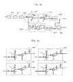
- FIG. 3is a block diagram illustrating the construction of an RF characteristic analyzer of FIG. 1 ;
- FIGS. 4 a to 4 care circuit diagrams of constituent elements constituting the RF characteristic analyzer of FIG. 3 .
- the CDMA base station systemincludes a base station processor 201 to take charge of an interface in a base station and control peripheral boards. It also includes an upper processor 202 communicatively coupled to the base station processor 201 for taking charge of an interface between the base station and an exchange (not illustrated). Next, a channel card 203 is provided to modulate/demodulate signals transmitted from/received by the base station.
- a transmitted frequency converter 204is provided to convert a transmitted frequency into an allocated use frequency band, and a transmitted power amplifier 206 is provided to amplify the signal to transmit at a rated power of the base station.
- the systemalso includes a transmitted frequency band filter 208 , which passes therethrough only the allocated frequency band (i.e., the transmitted frequency band to be used).
- the base station systemincludes a received frequency converter 205 , to convert a received frequency into a frequency band used in the base station.
- a receiving amplifier 207is coupled to the received frequency converter 205 to amplify a low-level signal from a terminal.
- the systemalso includes a received frequency band filter 209 , which passes therethrough only the allocated frequency band.
- a power level measuring device 210is included, and measures a power level of a final end of the base station, and an RF characteristic analyzer 211 included to monitor and analyze output signals of the transmitted frequency band filter and the received frequency converter.
- the RF characteristic analyzer 211is configured to transmit a result of its analysis to the base station processor.
- the operation of the CDMA base stationis preferably divided into four functions: (1) base station transmission; (2) base station reception; (3) output signal strength detection; and (4) RF characteristic analysis.
- the channel card 203which controls the transmitted/received signal modulation and demodulation, modulates the transmitted signal of the CDMA base station.
- the modulated signalthen passes through the transmitted frequency band filter 208 via the transmitted frequency converter 204 .
- the frequency converterconverts the transmitted signal to be transmitted into the proper frequency for use (i.e., the allocated use frequency).
- the transmitted power amplifier 206After the signal passes through the transmitted frequency converter 204 , it passes through the transmitted power amplifier 206 to increase the transmitted power to the rated power (i.e., the maximum power of the base station that can be transmitted within the range satisfying the characteristic of the base station).
- the signal outputted from transmitted power amplifier 206next passes through the transmitted frequency band filter 208 , which eliminates any unwanted frequencies from the signal, and is then transmitted through a transmission antenna 212 .
- the receiving function of the CDMA base stationis contrary to the transmission function.
- a signalis received through the receiving antenna 213 , and passes through the received frequency filter 209 . Only the allocated frequency band is outputted from the received frequency band filter 209 .
- the signal, having passed through the received frequency band filter 209is next amplified by the receiving amplifier 207 as much as is required based on the power of the received signal and the power required by the CDMA base station.
- the thusly amplified signalis then converted into a low frequency signal through the received frequency converter 205 .
- the signalis thus set at a frequency that is usable by the CDMA base station.
- the signal converted into the low frequencyis transmitted to and demodulated by the channel card 203 .
- the CDMA base stationmeasures the strength of the current transmitted signal of the final end using the power level measuring device 210 .
- the power level measuring devicedetects the strength of the transmitted output, and reports the measured strength to the base station processor 201 .
- the RF characteristic analyzer 211preferably monitors and analyzes the output signals of both the transmitted frequency band filter 208 and the received frequency converter 205 . If it determines that the call quality may deteriorate, it transmits an alarm signal to the base station processor so that an appropriate measure can be taken before the call quality deteriorates.
- the RF characteristic analyzer employed in the CDMA base stationcomprises an input/output circuit 301 , coupled to input/output the signals to be monitored, and to output the alarm signal.
- a transmission characteristic analyzing circuit 302is provided to monitor and analyze the output signal of the transmitted frequency band filter 208 in real time
- a reception characteristic analyzing circuit 303is provided to monitor and analyze the output signal of the received frequency converter 205 in real time.
- the RF characteristic analyzerfurther includes an alarm generating circuit 304 , which preferably receives analyzed data from the transmission characteristic analyzing circuit 302 and the reception characteristic analyzing circuit 303 , and generates an alarm message in accordance with the received data.
- a power supply circuit 500is preferably provided to supply power to the RF characteristic analyzer.
- the transmission characteristic analyzing circuit 302preferably comprises a first filter 401 , which is preferably a band rejection filter that eliminates a used base station transmission band signal.
- An analog-to-digital (A/D) converter 402is also provided, and converts an analog signal passing through the first band rejection) filter 401 into a digital signal.
- a second filter 403is provided to remove a prescribed frequency component.
- the second filter 403is preferably a low pass filter, to remove a high-frequency component, passing therethrough only a low frequency.
- the circuitalso preferably includes a differentiator 404 which determines whether a strength of a signal outputted from the A/D converter is gradually increased or decreased, and a sign changer 405 for changing a sign of an output signal of the differentiator. That is, if the signal received from the differentiator 404 is a negative number, the sign changer changes it to a positive number, while if the signal is a positive number, the sign changer changes it to a negative number.
- the circuitalso preferably includes an integrator 406 which outputs a positive integer value if the signal inputted thereto is larger than a specified threshold value, and noise removers 407 and 408 coupled to the sign changer 405 and the integrator 406 , respectively, for removing input noises.
- the circuitpreferably includes a logic gate 409 coupled to receive the outputs of each of the noise removers 407 , 408 .
- the reception characteristic analyzing circuit 303has the same construction as the transmission characteristic analyzing circuit 302 , except that the first filter 410 is preferably a band pass filter for passing therethrough a prescribed band of frequencies.
- the bandwidthis preferably 5 MHz, including a received intermediate frequency (IF) band.
- the transmitted signalis inputted to a monitoring port a of the base station through the input/output circuit 301 .
- the signalthen passes through the band rejection filter 401 of the transmission characteristic analyzing circuit 302 .
- the positive signalwhich is a normal signal existing in the actual band, is eliminated, and an unwanted wave signal, which includes unnecessary out-of-band signals, passes through the band rejection filter 401 .
- the band rejection filterpasses therethrough frequencies having the characteristics of ⁇ 1.25 MHz, ⁇ 1.98 MHz, ⁇ 2.25 MHz and greater than ⁇ 2.25 MHz from the used frequency of 1.23 MHz.
- the unwanted wave signalis then converted into a digital signal by the A/D converter 402 .
- the value of the digital signalis represented as a real number in proportion to the signal strength of the unwanted wave signal.
- the output signal of the A/D converter 402passes through the low pass filter 403 with its high-frequency component noise removed, and then passes through the differentiator 404 . At this time, the output value of the differentiator is given by
- Equation 1“Rf 1 ” denotes the value of a feedback resistor, and “Vs” denotes a voltage of the input terminal of the differentiator.
- the systemdetermines whether the signal strength of the input terminal of the differentiator (i.e., the real number) is gradually increasing. At this time, if the strength is gradually increasing, the sign of the output value is a negative number.
- the output of the differentiator 404then passes through the sign changer 405 . At this time, the output of the sign changer 405 is given by
- Equation 2“Rf2” denotes a feedback resistor
- the signalAfter passing through the sign changer 405 , the signal is inputted to the noise remover 407 , and an output value Vp 1 is outputted from the noise remover 407 with its sign clarified.
- an accurate high-level (i.e., 5V) valueis inputted to the input terminal of the alarm circuit 419 .
- the alarm circuit 419receives the output value Vp 1 . If the output value Vp 1 is “high”, the power supply Vcc is applied to a node V of the alarm circuit 419 to initiate a first indicator, for example turning on a yellow LED LY. A “high” signal is sent to node Va 1 of the alarm circuit 419 , and a first alarm message is consequently transmitted to the base station processor 201 through the input/output circuit 301 .
- the signal on a node O of the differentiator 404is inputted to the integrator 406 .
- the output function of the integratoris expressed by
- Equation 3“R” denotes the value of a resistor connected to a terminal V 2 of an amplifier in the differentiator, “V 2 ” denotes a threshold value determined by varying the value Rv in the integrator 406 , and “V 1 ” denotes an input signal of the integrator 406 .
- the output values Vp 1 and Vp 5are inputted to the logic gate 409 , and a value Vp 2 is outputted from the logic gate 409 .
- the value Vp 2becomes “high.”
- the value Vp 2is then inputted to the alarm circuit 420 , and thus a red LED LR is turned on, and a second alarm message is transmitted to the base station processor 201 through the input/output circuit 301 .
- the signal from the received frequency converter 205is inputted to a monitoring port b of the base station through the input/output circuit 301 .
- the signalthen passes through the band pass filter 410 of the reception characteristic analyzing circuit 303 .
- the 5 MHz band, including the IF bandpasses through the band pass filter 410 .
- the CDMA base station system as described hereinhas several advantages. For example, the call quality can be improved by receiving an advanced alarm message before any problem occurs in the base station, and thus enabling an appropriate measure to be taken. Also, the RF characteristic analysis can be performed by the base station itself without the necessity of a separate measuring equipment.
- the base station characteristic changecan be confirmed during the reliability test of the base station, and thus the system can be usefully adopted in mass production, thereby ensuring reliability.
Landscapes
- Engineering & Computer Science (AREA)
- Computer Networks & Wireless Communication (AREA)
- Signal Processing (AREA)
- Quality & Reliability (AREA)
- Physics & Mathematics (AREA)
- Electromagnetism (AREA)
- Mobile Radio Communication Systems (AREA)
- Monitoring And Testing Of Transmission In General (AREA)
Abstract
Description
denotes the output value of the differentiator. By the above equation, the sign of the output value is changed. Thus, if the sign were a negative value, it would change to a positive value. Specifically, the sign of the output value becomes positive if the unwanted wave of the base station transmission characteristic is gradually increasing, while otherwise, it becomes negative.
Claims (27)
Applications Claiming Priority (2)
| Application Number | Priority Date | Filing Date | Title |
|---|---|---|---|
| KR1019990057877AKR100314426B1 (en) | 1999-12-15 | 1999-12-15 | System for base station of Code Division Multiple Access |
| KR57877/1999 | 1999-12-15 |
Publications (2)
| Publication Number | Publication Date |
|---|---|
| US20010016503A1 US20010016503A1 (en) | 2001-08-23 |
| US7117022B2true US7117022B2 (en) | 2006-10-03 |
Family
ID=19626014
Family Applications (1)
| Application Number | Title | Priority Date | Filing Date |
|---|---|---|---|
| US09/735,547Expired - Fee RelatedUS7117022B2 (en) | 1999-12-15 | 2000-12-14 | CDMA base station system |
Country Status (2)
| Country | Link |
|---|---|
| US (1) | US7117022B2 (en) |
| KR (1) | KR100314426B1 (en) |
Cited By (2)
| Publication number | Priority date | Publication date | Assignee | Title |
|---|---|---|---|---|
| US20040204026A1 (en)* | 2003-04-09 | 2004-10-14 | Ar Card | Method, apparatus and system of configuring a wireless device based on location |
| US20130278421A1 (en)* | 2012-04-18 | 2013-10-24 | Qualcomm Incorporated | Bidirectional single-pin alarm interface |
Families Citing this family (29)
| Publication number | Priority date | Publication date | Assignee | Title |
|---|---|---|---|---|
| KR20010057357A (en)* | 1999-12-22 | 2001-07-04 | 박종섭 | Character verification apparatus of RF receiver in base station of CDMA communication system |
| KR20030055828A (en)* | 2001-12-27 | 2003-07-04 | 에스케이 텔레콤주식회사 | Mobile data communication system having improved modulator digital signal processor |
| KR100496061B1 (en)* | 2002-05-29 | 2005-06-16 | 에스케이 텔레콤주식회사 | Code domain analyzing system of cdma base station |
| US8320951B2 (en)* | 2004-03-12 | 2012-11-27 | Alcatel Lucent | Power sharing process in cellular network architecture |
| KR100576308B1 (en)* | 2004-04-01 | 2006-05-03 | 주식회사 지.아이.티 | Transmission Signal Strength Indicator Power Detector for Wideband Code Division Multiple Access Optical Repeater |
| US7366477B2 (en)* | 2004-05-06 | 2008-04-29 | Nokia Corporation | Redundancy version implementation for an uplink enhanced dedicated channel |
| AU2008222837B2 (en)* | 2007-03-06 | 2013-02-14 | Qualcomm Incorporated | System and method for spectrum management |
| US20090075644A1 (en)* | 2007-09-19 | 2009-03-19 | Adc Telecommunications, Inc. | System and method for selectively rejecting frequency bands in wireless communication systems |
| KR101032310B1 (en) | 2009-06-29 | 2011-05-06 | 한국항공우주연구원 | RF integrated measuring device for satellite |
| KR101006017B1 (en)* | 2010-02-10 | 2011-01-06 | 주식회사 건양기술공사 건축사사무소 | Porch drain of apartment which can reduce drainage noise |
| US12256233B2 (en) | 2013-03-15 | 2025-03-18 | Digital Global Systems, Inc. | Systems and methods for automated financial settlements for dynamic spectrum sharing |
| US10257729B2 (en) | 2013-03-15 | 2019-04-09 | DGS Global Systems, Inc. | Systems, methods, and devices having databases for electronic spectrum management |
| US10231206B2 (en) | 2013-03-15 | 2019-03-12 | DGS Global Systems, Inc. | Systems, methods, and devices for electronic spectrum management for identifying signal-emitting devices |
| US10299149B2 (en) | 2013-03-15 | 2019-05-21 | DGS Global Systems, Inc. | Systems, methods, and devices for electronic spectrum management |
| US11646918B2 (en) | 2013-03-15 | 2023-05-09 | Digital Global Systems, Inc. | Systems, methods, and devices for electronic spectrum management for identifying open space |
| US9078162B2 (en) | 2013-03-15 | 2015-07-07 | DGS Global Systems, Inc. | Systems, methods, and devices for electronic spectrum management |
| US12356206B2 (en) | 2013-03-15 | 2025-07-08 | Digital Global Systems, Inc. | Systems and methods for automated financial settlements for dynamic spectrum sharing |
| US10271233B2 (en) | 2013-03-15 | 2019-04-23 | DGS Global Systems, Inc. | Systems, methods, and devices for automatic signal detection with temporal feature extraction within a spectrum |
| US10257727B2 (en) | 2013-03-15 | 2019-04-09 | DGS Global Systems, Inc. | Systems methods, and devices having databases and automated reports for electronic spectrum management |
| US10219163B2 (en) | 2013-03-15 | 2019-02-26 | DGS Global Systems, Inc. | Systems, methods, and devices for electronic spectrum management |
| US10237770B2 (en) | 2013-03-15 | 2019-03-19 | DGS Global Systems, Inc. | Systems, methods, and devices having databases and automated reports for electronic spectrum management |
| US10257728B2 (en) | 2013-03-15 | 2019-04-09 | DGS Global Systems, Inc. | Systems, methods, and devices for electronic spectrum management |
| US12205477B2 (en) | 2017-01-23 | 2025-01-21 | Digital Global Systems, Inc. | Unmanned vehicle recognition and threat management |
| US10529241B2 (en) | 2017-01-23 | 2020-01-07 | Digital Global Systems, Inc. | Unmanned vehicle recognition and threat management |
| US10498951B2 (en) | 2017-01-23 | 2019-12-03 | Digital Global Systems, Inc. | Systems, methods, and devices for unmanned vehicle detection |
| US10459020B2 (en) | 2017-01-23 | 2019-10-29 | DGS Global Systems, Inc. | Systems, methods, and devices for automatic signal detection based on power distribution by frequency over time within a spectrum |
| US10700794B2 (en) | 2017-01-23 | 2020-06-30 | Digital Global Systems, Inc. | Systems, methods, and devices for automatic signal detection based on power distribution by frequency over time within an electromagnetic spectrum |
| US12183213B1 (en) | 2017-01-23 | 2024-12-31 | Digital Global Systems, Inc. | Unmanned vehicle recognition and threat management |
| US10943461B2 (en)* | 2018-08-24 | 2021-03-09 | Digital Global Systems, Inc. | Systems, methods, and devices for automatic signal detection based on power distribution by frequency over time |
Citations (11)
| Publication number | Priority date | Publication date | Assignee | Title |
|---|---|---|---|---|
| US4989204A (en)* | 1988-02-10 | 1991-01-29 | Nec Corporation | High throughput communication method and system for a digital mobile station when crossing a zone boundary during a session |
| US5255307A (en)* | 1992-05-07 | 1993-10-19 | Sony Electronics Inc. | Status indicator control for cellular mobile telephone system |
| US5423071A (en)* | 1990-11-02 | 1995-06-06 | Telenokia Oy | Monitoring and alarm circuitry for a base station transmitting supervising signals to one or more mobile radio stations |
| US5442811A (en)* | 1992-12-14 | 1995-08-15 | Fujitsu Limited | Loop testable radio transmitters/receivers |
| US5768689A (en)* | 1995-04-03 | 1998-06-16 | Telefonaktiebolaget Lm Ericsson | Transceiver tester |
| US5890056A (en)* | 1996-07-09 | 1999-03-30 | Lucent Technologies, Inc. | Channel usage monitoring arrangement for base station |
| US5978659A (en)* | 1995-12-30 | 1999-11-02 | Samsung Electronics Co., Ltd. | Radio characteristic evaluating apparatus of mobile telecommunication device |
| US6112070A (en)* | 1996-04-23 | 2000-08-29 | Oki Electric Industry Co., Ltd. | High frequency receiving circuit for mobile communication apparatus |
| US6157183A (en)* | 1994-12-22 | 2000-12-05 | Anritsu Company | Two port handheld vector network analyzer with frequency monitor mode |
| US6529712B1 (en)* | 1999-08-25 | 2003-03-04 | Conexant Systems, Inc. | System and method for amplifying a cellular radio signal |
| US6842614B2 (en)* | 2002-02-04 | 2005-01-11 | Agilent Technologies, Inc. | Network analyzer for measuring the antenna return loss in a live cellular network |
- 1999
- 1999-12-15KRKR1019990057877Apatent/KR100314426B1/ennot_activeExpired - Fee Related
- 2000
- 2000-12-14USUS09/735,547patent/US7117022B2/ennot_activeExpired - Fee Related
Patent Citations (11)
| Publication number | Priority date | Publication date | Assignee | Title |
|---|---|---|---|---|
| US4989204A (en)* | 1988-02-10 | 1991-01-29 | Nec Corporation | High throughput communication method and system for a digital mobile station when crossing a zone boundary during a session |
| US5423071A (en)* | 1990-11-02 | 1995-06-06 | Telenokia Oy | Monitoring and alarm circuitry for a base station transmitting supervising signals to one or more mobile radio stations |
| US5255307A (en)* | 1992-05-07 | 1993-10-19 | Sony Electronics Inc. | Status indicator control for cellular mobile telephone system |
| US5442811A (en)* | 1992-12-14 | 1995-08-15 | Fujitsu Limited | Loop testable radio transmitters/receivers |
| US6157183A (en)* | 1994-12-22 | 2000-12-05 | Anritsu Company | Two port handheld vector network analyzer with frequency monitor mode |
| US5768689A (en)* | 1995-04-03 | 1998-06-16 | Telefonaktiebolaget Lm Ericsson | Transceiver tester |
| US5978659A (en)* | 1995-12-30 | 1999-11-02 | Samsung Electronics Co., Ltd. | Radio characteristic evaluating apparatus of mobile telecommunication device |
| US6112070A (en)* | 1996-04-23 | 2000-08-29 | Oki Electric Industry Co., Ltd. | High frequency receiving circuit for mobile communication apparatus |
| US5890056A (en)* | 1996-07-09 | 1999-03-30 | Lucent Technologies, Inc. | Channel usage monitoring arrangement for base station |
| US6529712B1 (en)* | 1999-08-25 | 2003-03-04 | Conexant Systems, Inc. | System and method for amplifying a cellular radio signal |
| US6842614B2 (en)* | 2002-02-04 | 2005-01-11 | Agilent Technologies, Inc. | Network analyzer for measuring the antenna return loss in a live cellular network |
Cited By (4)
| Publication number | Priority date | Publication date | Assignee | Title |
|---|---|---|---|---|
| US20040204026A1 (en)* | 2003-04-09 | 2004-10-14 | Ar Card | Method, apparatus and system of configuring a wireless device based on location |
| US7421276B2 (en)* | 2003-04-09 | 2008-09-02 | Nortel Networks Limited | Method, apparatus and system of configuring a wireless device based on location |
| US20130278421A1 (en)* | 2012-04-18 | 2013-10-24 | Qualcomm Incorporated | Bidirectional single-pin alarm interface |
| US9013305B2 (en)* | 2012-04-18 | 2015-04-21 | Qualcomm Incorporated | Bidirectional single-pin alarm interface |
Also Published As
| Publication number | Publication date |
|---|---|
| KR20010056422A (en) | 2001-07-04 |
| US20010016503A1 (en) | 2001-08-23 |
| KR100314426B1 (en) | 2001-11-17 |
Similar Documents
| Publication | Publication Date | Title |
|---|---|---|
| US7117022B2 (en) | CDMA base station system | |
| US7519112B2 (en) | Testing device and method for providing receiver overload protection during transceiver testing | |
| US6313874B1 (en) | Method and apparatus for direct detection of communication system leakage signals | |
| JP3061005B2 (en) | Transceiver with antenna abnormality detection function | |
| US7659708B2 (en) | Broadcast receiver having integrated spectrum analysis | |
| KR20060014730A (en) | Time Division Duplex Transmission / Reception Unit Utilizing Transmit and Receive Mode Simultaneously and Self-Diagnostic Method | |
| US7982467B2 (en) | Built-in test for high-speed electrical networks | |
| EP0208530B1 (en) | Squelch detecting circuit with squelch start determining means | |
| US11128390B1 (en) | Antenna-free receiver bit error rate testing | |
| JP2009265108A (en) | Integrated circuit comprising transmission channel equipped with integrated independent tester | |
| US5444862A (en) | Circuit for stopping data transmission responding to low level and rapid fall of received electric field | |
| KR20030024285A (en) | Operating Point Determination Apparatus and method for High Power Amplifier of Communication and Broadcasting Satellite Transponder | |
| CN113890561B (en) | Electronic equipment and radio frequency circuit thereof | |
| KR100355773B1 (en) | Apparatus for diagnosing oscillation state of wireless repeater | |
| KR100400921B1 (en) | Apparatus and method for diagnostic of RF block by using receiving auto gain control | |
| KR100336844B1 (en) | Remote monitoring system of base station for wireless communication device | |
| FI86935B (en) | FOERFARANDE FOER IDENTIFIERING AV EN OEVERVAKNINGSSIGNAL PAO BASSTATION I RADIOTELEFONSYSTEMET. | |
| US20070149155A1 (en) | System and method for detecting narrow bandwidth signal content to determine channel occupancy | |
| KR20000046232A (en) | Device for frequency conversion loop for self-examination of communicators using difference frequencies | |
| US4414568A (en) | Device for the measurement, in operation, of non-linearity products in a television transmitter | |
| JP2531377B2 (en) | Modulation method identification circuit | |
| KR100416338B1 (en) | Device for monitoring a repeater by measurement of field strength | |
| JP2834043B2 (en) | Received electric field monitoring device | |
| CN118802030A (en) | Wireless microphone frequency management method and system | |
| CN117615352A (en) | VDES transceiver equipment test system architecture |
Legal Events
| Date | Code | Title | Description |
|---|---|---|---|
| AS | Assignment | Owner name:LG ELECTRONICS, INC., KOREA, REPUBLIC OF Free format text:ASSIGNMENT OF ASSIGNORS INTEREST;ASSIGNOR:KANG, SEOK MOON;REEL/FRAME:011375/0421 Effective date:20001212 | |
| AS | Assignment | Owner name:LG NORTEL CO., LTD., KOREA, REPUBLIC OF Free format text:ASSIGNMENT OF ASSIGNORS INTEREST;ASSIGNOR:LG ELECTRONICS INC.;REEL/FRAME:018296/0720 Effective date:20060710 | |
| FEPP | Fee payment procedure | Free format text:PAYOR NUMBER ASSIGNED (ORIGINAL EVENT CODE: ASPN); ENTITY STATUS OF PATENT OWNER: LARGE ENTITY | |
| FPAY | Fee payment | Year of fee payment:4 | |
| AS | Assignment | Owner name:LG-ERICSSON CO., LTD., KOREA, REPUBLIC OF Free format text:CHANGE OF NAME;ASSIGNOR:LG-NORTEL CO., LTD.;REEL/FRAME:025948/0842 Effective date:20100630 | |
| FEPP | Fee payment procedure | Free format text:PAYER NUMBER DE-ASSIGNED (ORIGINAL EVENT CODE: RMPN); ENTITY STATUS OF PATENT OWNER: LARGE ENTITY Free format text:PAYOR NUMBER ASSIGNED (ORIGINAL EVENT CODE: ASPN); ENTITY STATUS OF PATENT OWNER: LARGE ENTITY | |
| FPAY | Fee payment | Year of fee payment:8 | |
| FEPP | Fee payment procedure | Free format text:MAINTENANCE FEE REMINDER MAILED (ORIGINAL EVENT CODE: REM.) | |
| LAPS | Lapse for failure to pay maintenance fees | Free format text:PATENT EXPIRED FOR FAILURE TO PAY MAINTENANCE FEES (ORIGINAL EVENT CODE: EXP.); ENTITY STATUS OF PATENT OWNER: LARGE ENTITY | |
| STCH | Information on status: patent discontinuation | Free format text:PATENT EXPIRED DUE TO NONPAYMENT OF MAINTENANCE FEES UNDER 37 CFR 1.362 | |
| FP | Lapsed due to failure to pay maintenance fee | Effective date:20181003 |