US7116912B2 - Method and apparatus for pluggable fiber optic modules - Google Patents
Method and apparatus for pluggable fiber optic modulesDownload PDFInfo
- Publication number
- US7116912B2 US7116912B2US10/118,761US11876102AUS7116912B2US 7116912 B2US7116912 B2US 7116912B2US 11876102 AUS11876102 AUS 11876102AUS 7116912 B2US7116912 B2US 7116912B2
- Authority
- US
- United States
- Prior art keywords
- printed circuit
- circuit board
- fiber optic
- optical
- pcb
- Prior art date
- Legal status (The legal status is an assumption and is not a legal conclusion. Google has not performed a legal analysis and makes no representation as to the accuracy of the status listed.)
- Ceased, expires
Links
- 239000000835fiberSubstances0.000titleclaimsabstractdescription259
- 238000000034methodMethods0.000titledescription13
- 230000005693optoelectronicsEffects0.000claimsabstractdescription64
- 230000003287optical effectEffects0.000claimsdescription217
- 239000013307optical fiberSubstances0.000claimsdescription59
- 229910000679solderInorganic materials0.000claimsdescription51
- 239000004033plasticSubstances0.000claimsdescription25
- 230000008878couplingEffects0.000claimsdescription22
- 238000010168coupling processMethods0.000claimsdescription22
- 238000005859coupling reactionMethods0.000claimsdescription22
- 239000002184metalSubstances0.000claimsdescription17
- 230000005672electromagnetic fieldEffects0.000claimsdescription6
- MPCDNZSLJWJDNW-UHFFFAOYSA-N1,2,3-trichloro-4-(3,5-dichlorophenyl)benzeneChemical compoundClC1=CC(Cl)=CC(C=2C(=C(Cl)C(Cl)=CC=2)Cl)=C1MPCDNZSLJWJDNW-UHFFFAOYSA-N0.000description86
- BQENMISTWGTJIJ-UHFFFAOYSA-N2,3,3',4,5-pentachlorobiphenylChemical compoundClC1=CC=CC(C=2C(=C(Cl)C(Cl)=C(Cl)C=2)Cl)=C1BQENMISTWGTJIJ-UHFFFAOYSA-N0.000description83
- 239000004593EpoxySubstances0.000description18
- 239000003292glueSubstances0.000description13
- 230000006854communicationEffects0.000description9
- 238000004891communicationMethods0.000description9
- 238000004519manufacturing processMethods0.000description7
- 239000004065semiconductorSubstances0.000description7
- 239000003990capacitorSubstances0.000description6
- 238000002955isolationMethods0.000description4
- 239000000463materialSubstances0.000description4
- 230000008901benefitEffects0.000description3
- 238000012986modificationMethods0.000description3
- 230000004048modificationEffects0.000description3
- 230000003068static effectEffects0.000description3
- 239000000758substrateSubstances0.000description3
- 230000005540biological transmissionEffects0.000description2
- 238000010586diagramMethods0.000description2
- 238000001746injection mouldingMethods0.000description2
- 230000007246mechanismEffects0.000description2
- 230000004044responseEffects0.000description2
- 238000005476solderingMethods0.000description2
- 239000000853adhesiveSubstances0.000description1
- 230000001070adhesive effectEffects0.000description1
- 230000003321amplificationEffects0.000description1
- 238000005452bendingMethods0.000description1
- 230000007175bidirectional communicationEffects0.000description1
- 238000000071blow mouldingMethods0.000description1
- 239000000919ceramicSubstances0.000description1
- 239000004020conductorSubstances0.000description1
- 238000010276constructionMethods0.000description1
- 238000001514detection methodMethods0.000description1
- 230000009977dual effectEffects0.000description1
- 230000005684electric fieldEffects0.000description1
- 238000005242forgingMethods0.000description1
- 230000004927fusionEffects0.000description1
- 239000007924injectionSubstances0.000description1
- 238000003780insertionMethods0.000description1
- 230000037431insertionEffects0.000description1
- 239000012212insulatorSubstances0.000description1
- 238000003754machiningMethods0.000description1
- 230000013011matingEffects0.000description1
- 238000002844meltingMethods0.000description1
- 230000008018meltingEffects0.000description1
- 230000007176multidirectional communicationEffects0.000description1
- 230000006855networkingEffects0.000description1
- 239000012811non-conductive materialSubstances0.000description1
- 238000003199nucleic acid amplification methodMethods0.000description1
- 239000004417polycarbonateSubstances0.000description1
- 229920000515polycarbonatePolymers0.000description1
- 230000008569processEffects0.000description1
- 230000005855radiationEffects0.000description1
- 238000011084recoveryMethods0.000description1
- 238000000926separation methodMethods0.000description1
- 239000011343solid materialSubstances0.000description1
- 229910001220stainless steelInorganic materials0.000description1
- 239000010935stainless steelSubstances0.000description1
- 229920001169thermoplasticPolymers0.000description1
- 239000004416thermosoftening plasticSubstances0.000description1
- 230000002463transducing effectEffects0.000description1
- 238000001721transfer mouldingMethods0.000description1
- 239000001993waxSubstances0.000description1
- 238000003466weldingMethods0.000description1
Images

Classifications
- G—PHYSICS
- G02—OPTICS
- G02B—OPTICAL ELEMENTS, SYSTEMS OR APPARATUS
- G02B6/00—Light guides; Structural details of arrangements comprising light guides and other optical elements, e.g. couplings
- G02B6/24—Coupling light guides
- G02B6/42—Coupling light guides with opto-electronic elements
- G02B6/4201—Packages, e.g. shape, construction, internal or external details
- G02B6/4204—Packages, e.g. shape, construction, internal or external details the coupling comprising intermediate optical elements, e.g. lenses, holograms
- G02B6/4214—Packages, e.g. shape, construction, internal or external details the coupling comprising intermediate optical elements, e.g. lenses, holograms the intermediate optical element having redirecting reflective means, e.g. mirrors, prisms for deflecting the radiation from horizontal to down- or upward direction toward a device
- G—PHYSICS
- G02—OPTICS
- G02B—OPTICAL ELEMENTS, SYSTEMS OR APPARATUS
- G02B6/00—Light guides; Structural details of arrangements comprising light guides and other optical elements, e.g. couplings
- G02B6/24—Coupling light guides
- G02B6/42—Coupling light guides with opto-electronic elements
- G02B6/4201—Packages, e.g. shape, construction, internal or external details
- G02B6/4219—Mechanical fixtures for holding or positioning the elements relative to each other in the couplings; Alignment methods for the elements, e.g. measuring or observing methods especially used therefor
- G02B6/4236—Fixing or mounting methods of the aligned elements
- G02B6/424—Mounting of the optical light guide
- G—PHYSICS
- G02—OPTICS
- G02B—OPTICAL ELEMENTS, SYSTEMS OR APPARATUS
- G02B6/00—Light guides; Structural details of arrangements comprising light guides and other optical elements, e.g. couplings
- G02B6/24—Coupling light guides
- G02B6/42—Coupling light guides with opto-electronic elements
- G02B6/4201—Packages, e.g. shape, construction, internal or external details
- G02B6/4246—Bidirectionally operating package structures
- G—PHYSICS
- G02—OPTICS
- G02B—OPTICAL ELEMENTS, SYSTEMS OR APPARATUS
- G02B6/00—Light guides; Structural details of arrangements comprising light guides and other optical elements, e.g. couplings
- G02B6/24—Coupling light guides
- G02B6/42—Coupling light guides with opto-electronic elements
- G02B6/4201—Packages, e.g. shape, construction, internal or external details
- G02B6/4251—Sealed packages
- G02B6/4253—Sealed packages by embedding housing components in an adhesive or a polymer material
- G—PHYSICS
- G02—OPTICS
- G02B—OPTICAL ELEMENTS, SYSTEMS OR APPARATUS
- G02B6/00—Light guides; Structural details of arrangements comprising light guides and other optical elements, e.g. couplings
- G02B6/24—Coupling light guides
- G02B6/42—Coupling light guides with opto-electronic elements
- G02B6/4201—Packages, e.g. shape, construction, internal or external details
- G02B6/4256—Details of housings
- G02B6/4257—Details of housings having a supporting carrier or a mounting substrate or a mounting plate
- G—PHYSICS
- G02—OPTICS
- G02B—OPTICAL ELEMENTS, SYSTEMS OR APPARATUS
- G02B6/00—Light guides; Structural details of arrangements comprising light guides and other optical elements, e.g. couplings
- G02B6/24—Coupling light guides
- G02B6/42—Coupling light guides with opto-electronic elements
- G02B6/4201—Packages, e.g. shape, construction, internal or external details
- G02B6/4256—Details of housings
- G02B6/426—Details of housings mounting, engaging or coupling of the package to a board, a frame or a panel
- G02B6/4261—Packages with mounting structures to be pluggable or detachable, e.g. having latches or rails
- G—PHYSICS
- G02—OPTICS
- G02B—OPTICAL ELEMENTS, SYSTEMS OR APPARATUS
- G02B6/00—Light guides; Structural details of arrangements comprising light guides and other optical elements, e.g. couplings
- G02B6/24—Coupling light guides
- G02B6/42—Coupling light guides with opto-electronic elements
- G02B6/4201—Packages, e.g. shape, construction, internal or external details
- G02B6/4256—Details of housings
- G02B6/4262—Details of housings characterised by the shape of the housing
- G02B6/4263—Details of housings characterised by the shape of the housing of the transisitor outline [TO] can type
- G—PHYSICS
- G02—OPTICS
- G02B—OPTICAL ELEMENTS, SYSTEMS OR APPARATUS
- G02B6/00—Light guides; Structural details of arrangements comprising light guides and other optical elements, e.g. couplings
- G02B6/24—Coupling light guides
- G02B6/42—Coupling light guides with opto-electronic elements
- G02B6/4201—Packages, e.g. shape, construction, internal or external details
- G02B6/4274—Electrical aspects
- G02B6/4277—Protection against electromagnetic interference [EMI], e.g. shielding means
- G—PHYSICS
- G02—OPTICS
- G02B—OPTICAL ELEMENTS, SYSTEMS OR APPARATUS
- G02B6/00—Light guides; Structural details of arrangements comprising light guides and other optical elements, e.g. couplings
- G02B6/24—Coupling light guides
- G02B6/42—Coupling light guides with opto-electronic elements
- G02B6/4201—Packages, e.g. shape, construction, internal or external details
- G02B6/4274—Electrical aspects
- G02B6/428—Electrical aspects containing printed circuit boards [PCB]
- G—PHYSICS
- G02—OPTICS
- G02B—OPTICAL ELEMENTS, SYSTEMS OR APPARATUS
- G02B6/00—Light guides; Structural details of arrangements comprising light guides and other optical elements, e.g. couplings
- G02B6/24—Coupling light guides
- G02B6/42—Coupling light guides with opto-electronic elements
- G02B6/4201—Packages, e.g. shape, construction, internal or external details
- G02B6/4274—Electrical aspects
- G02B6/4284—Electrical aspects of optical modules with disconnectable electrical connectors
- G—PHYSICS
- G02—OPTICS
- G02B—OPTICAL ELEMENTS, SYSTEMS OR APPARATUS
- G02B6/00—Light guides; Structural details of arrangements comprising light guides and other optical elements, e.g. couplings
- G02B6/24—Coupling light guides
- G02B6/42—Coupling light guides with opto-electronic elements
- G02B6/4292—Coupling light guides with opto-electronic elements the light guide being disconnectable from the opto-electronic element, e.g. mutually self aligning arrangements
Definitions
- This inventionrelates to fiber optic modules.
- Fiber optic modulesinterface optical fibers to electronic circuitry transducing communication by light or photons with communication by electrical signals.
- a fiber optic modulemay be a fiber optic receiver, transmitter or transceiver including both receive and transmit functions.
- the fiber optic receiver, transmitter and transceivereach have optical elements (OE) and electrical elements (EE).
- the fiber optic transmitter OEincludes an emitter (such as a semiconductor LED or Laser) mounted in a package and an optical coupling element for coupling light or photons from the OE into the optical fiber.
- the type of semiconductor laser(light amplification by stimulated emission of radiation) may be a vertical cavity surface emitting laser (VCSEL).
- the fiber optic receiver OEincludes a photodetector (such as a photodiode) mounted in a package and an optical coupling element for coupling light or photons from the optical fiber into the photodetector.
- the EE for eachincludes integrated circuits and passive elements mounted on a substrate such as a printed circuit board (PCB) or ceramic.
- PCBprinted circuit board
- the OE and EEare connected electrically at the emitter and photodetector.
- the fiber optic transceiverIn order to reduce EMI, shielding of the electrical components is required which is usually accomplished by attaching a metal shield to the substrate of the fiber optic module and connecting it to ground. In order to avoid electronic crosstalk and EMI, the fiber optic transceiver usually employs separate components and separate shielding of fiber optic receiver and fiber optic transmitter components. In order to avoid optical crosstalk where light or photons can interfere between communication channels, the fiber optic transceiver usually employs separate optical elements for coupling light or photons into and out of the optical fiber for fiber optic receiver and fiber optic transmitter. Using separate optical elements requires additional components and increases the costs of fiber optic transceivers. It is desirable to reduce the component count of fiber optic transceivers such that they are less expensive to manufacture.
- the form factor or size of the fiber optic moduleis of concern.
- the fiber optic transceiver, receiver, and transmitterutilized horizontal boards or substrates which mounted parallel with a system printed circuit board utilized significant footprint or board space.
- the horizontal boardsprovided nearly zero optical crosstalk and minimal electronic crosstalk when properly shielded.
- the horizontal boards, parallel to the system printed circuit boardrequired large spacing between optical fiber connectors to make the connection to the optical fibers. While this may have been satisfactory for early systems using minimal fiber optic communication, the trend is towards greater usage of fiber optic communication requiring improved connectivity and smaller optical fiber connectors to more densely pack them on a system printed circuit board.
- the OEis desirable to minimize the size of system printed circuit boards (PCBs) and accordingly it is desirable to reduce the footprint of the fiber optic module which will attach to such system PCBs.
- PCBssystem printed circuit boards
- the desire for tighter interconnect leads of fiber optic cablesrestricts the size of the OE's.
- the header dimension of the interconnect leadis normally 5.6 mm.
- the two optical fibersare separated by a distance of only 0.75 mm. This severely restricts the method of coupling light or photons from the OE into and out of fiber optic cables.
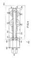
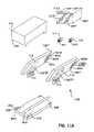
- FIG. 1is a simplified top cutaway view of a first embodiment of the invention.
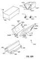
- FIG. 2is an exploded view of the first embodiment of the invention.
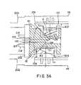
- FIG. 3Ais a cross-sectional view from the top of the optic block for the first embodiment of the invention.
- FIG. 3Bis a front side perspective view from the left of the optic block for the first embodiment of the invention.
- FIG. 3Cis a frontal view of the optic block for the first embodiment of the invention.
- FIG. 3Dis a back side perspective view from the right of the optic block for the first embodiment of the invention.
- FIG. 3Eis a back view of the optic block for the first embodiment of the invention.
- FIG. 3Fis a right side view of the optic block for the first embodiment of the invention.
- FIG. 3Gis a left side view of the optic block for the first embodiment of the invention.
- FIG. 3His a cross-sectional view of the optic block for the first embodiment of the invention.
- FIG. 3Iis a magnified cross-sectional view of the alignment post of the optic block.
- FIG. 4is a simplified top cutaway view of another embodiment of the invention.
- FIG. 5Ais an exploded view of the embodiment of the invention of FIG. 4 .
- FIG. 5Bis an exploded view of an alternate embodiment of the invention of FIG. 4 .
- FIG. 5Cis an exploded view of another alternate embodiment of the invention of FIG. 4 .
- FIG. 5Dis an exploded view of another alternate embodiment of the invention of FIG. 4 .
- FIG. 6Ais a cross-sectional view from the top of the optic block for embodiments of the invention.
- FIG. 6Bis a front side view of the optic block for the embodiments of the invention.
- FIG. 6Cis a back side view of the optic block for the embodiments of the invention.
- FIG. 6Dis a top side view of the optic block for the embodiments of the invention.
- FIG. 7Ais a top view of a manufacturing step of the invention.
- FIG. 7Bis a side view of a manufacturing step of the invention.
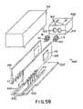
- FIG. 8Ais an exploded view of another embodiment of the invention.
- FIG. 8Bis perspective view of an alternate baseplate for embodiments of the invention.
- FIG. 8Cis a rear cross sectional view of the assembled invention illustrated in FIG. 8A .
- FIG. 9Ais an exploded view of another embodiment of the invention.
- FIG. 9Bis a rear cross sectional view of the assembled invention illustrated in FIG. 9A .
- FIG. 9Cillustrates an alternate embodiment of a single ground plane for a printed circuit board.
- FIG. 9Dillustrates an alternate embodiment of a single ground plane for a printed circuit board.
- FIG. 9Eillustrates an alternate embodiment of a ground plane sandwiched between layers in a multilayer printed circuit board.
- FIG. 10Ais an exploded view of another embodiment of the invention.
- FIG. 10Bis a rear cross sectional view of the assembled invention illustrated in FIG. 10A .
- FIG. 11Ais an exploded view of another embodiment of the invention.
- FIG. 11Bis a rear cross sectional view of the assembled invention illustrated in FIG. 11A .
- FIG. 12Ais an exploded view of another embodiment of the invention.
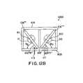
- FIG. 12Bis a rear cross sectional view of the assembled invention illustrated in FIG. 12A .
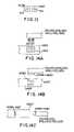
- FIG. 13illustrates a receive optical block and a transmit optical block as an alternative to a single optical block.
- FIG. 14Aillustrates how the pin configuration of the fiber optic modules can plug into a socket on a host printed circuit board.
- FIG. 14Billustrates how a socket configuration of the fiber optic modules can plug into a socket on a host printed circuit board.
- FIG. 14Cillustrates how a socket configuration of the fiber optic modules can horizontally plug into a socket on a host printed circuit board.
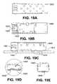
- FIG. 15Aillustrates a bottom perspective view of an alternate embodiment of the shielded housing or cover and base of the invention.
- FIG. 15Billustrates a rear cross sectional view of the assembled invention illustrated in FIG. 10A substituting the alternate embodiment of the shielded housing or cover of FIG. 15A .
- FIG. 15Cillustrates a rear cross sectional view of the alternate embodiment of the shielded housing or cover of FIG. 15A .
- FIG. 15Dillustrates a cross sectional view of another alternate embodiment of the shielded housing or cover.
- FIG. 15Eillustrates a cross sectional view of another alternate embodiment of the shielded housing or cover.
- FIG. 15Fillustrates a cross sectional view of another alternate embodiment of the shielded housing or cover.
- FIG. 15Gillustrates a cross sectional view of another alternate embodiment of the shielded housing or cover.
- FIG. 16Aillustrates a rear cross sectional view of an assembled alternate embodiment of the invention.
- FIG. 16Billustrates a rear cross sectional view of an assembled alternate embodiment of the invention.
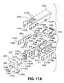
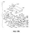
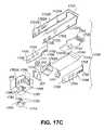
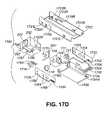
- FIGS. 17A–17Dillustrate exploded perspective views of an embodiment of the invention.
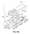
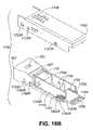
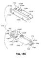
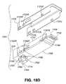
- FIGS. 18A–18Dillustrate a perspective views of the embodiment of the invention illustrated in FIGS. 17A–17D without the cover/housing assembled thereto.
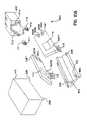
- FIGS. 19A–19Eare views of an exemplary cage assembly or module receptacle for fiber optic modules.
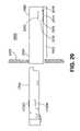
- FIG. 20is a side view of an embodiment of a fiber optic module and an exemplary host connector without the exemplary cage assembly of FIGS. 19A–19E .
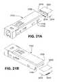
- FIGS. 21A–21Dare perspective views of an embodiment of a fiber optic module and an exemplary host connector without the exemplary cage assembly of FIGS. 19A–19E .
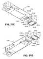
- FIGS. 22A–22Bare cross section views illustrating an embodiment of a fiber optic module coupling to the exemplary host connector of FIGS. 20 , 21 A– 21 D and the exemplary cage assembly of FIGS. 19A–19E .
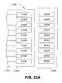
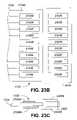
- FIGS. 23A–23Cillustrate an example of how an electrical connection between the interface printed circuit board of an embodiment of the fiber optic module and the host connector of a host printed circuit board is formed.
- the embodiments of the inventioninclude a method, apparatus and system for vertical board construction of fiber optic transmitters, receivers and transceivers.
- fiber optic transmitter and receiver electrical elementsare implemented on at least two separate printed circuit boards (PCBs) in a fiber optic module.
- the separate boardsare arranged within the fiber optic module to reduce the footprint of the fiber optic module.
- bending light or photons through ninety degrees, the light transmitter (a packaged type of emitter) and a light receiver (a packaged type of photodetector)are each mounted substantially perpendicular to the transmit and receive boards respectively such that their active areas are nearly facing each other but offset.
- a single optical blockcan be used to implement lenses and reflecting surfaces to minimize manufacturing costs.
- the light receiver and light transmitterare mounted offset from each other in the optical block in order to avoid optical cross talk.
- the light transmitter (emitter) and the light receiver (photodetector)are each mounted substantially parallel with the transmit and receive boards respectively, the optical axis of transmitter and receiver and the connection to the optical fibers.
- the separate receive and transmit boardscan be provided with ground planes in order to minimize electrical cross talk.
- Preferably the ground planes on the back sides of the printed circuit boardsface each other.
- a module outer shielded housing or cover, manufactured out of metal or metal plated plastic,provides further shielding for EMI.
- the separate boardsmay be extended to support multiple channels or multiple parallel fibers such as in a ribbon optical fiber cable. Manufacturing steps of the boards for the fiber optic module are disclosed to provide reduced manufacturing costs.
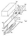
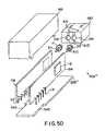
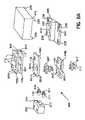
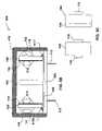
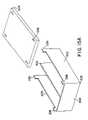
- FIG. 1illustrates a fiber optic module 100 coupling to a pair of fiber optic cables 101 .
- Fiber optic module 100includes an optical block 102 and an electrical element 104 .
- the optical block 102may also be referred to as a nose, an optical port, an alignment block, an optical connector, an optical receptacle or receptacle.
- the optical block 102can interface to an optical connector such as an LC, MT-RJ or VF-45 optical connector.
- the electrical element 104includes a transmit printed circuit board (PCB) 106 , a receive PCB 108 , an optional internal shield 109 , a light transmitter 110 , a light receiver 111 , and a shielded housing or cover 119 .
- the light transmitter 110 and light receiver 111are optoelectronic devices for communicating with optical fibers using light of various wavelengths or photons.
- An optoelectronic deviceis a device which can convert or transduce light or photons into an electrical signal or an electrical signal into light or photons.
- the transmitter 110is a packaged emitter, that converts an electrical signal into emitting light or photons, such as a semiconductor laser or LED, preferably packaged in a TO can.
- the receiver 111is a packaged photodetector, that detects or receives light or photons and converts it into an electrical signal, such as a photo diode, preferably package in a TO can. However other packages, housings or covers, or optoelectronic devices for receiving and transmitting light or photon may be used for the receiver 111 or transmitter 110 .
- Each of the optoelectronic devices, receiver 111 and transmitter 110have terminals.
- terminals of one or more optoelectronic devicescouple to thruholes of the PCB 106 or PCB 108 or both.
- terminals of one or more optoelectronic devicescouple to an edge connector of the PCB 106 or PCB 108 or both.
- the transmit PCB 106includes electrical components 112 (transmitter integrated circuit (laser driver), resistors, capacitors and other passive or active electrical components), pins 113 , and a ground plane 114 .
- the electrical components 112control the transmitter 110 and buffer the data signal received from a system for transmission over an optical fiber.
- the receive PCB 108includes electrical components 116 (receiver integrated circuit (transimpedance amplifier and post amplifier), resistors, capacitors and other passive or active electrical components), pins 117 , and a ground plane 118 .
- the electrical components 116control the receiver 111 and buffer the data signal received from an optical fiber.
- the ground planes 114 and 118 and the shielded housing or cover 119are coupled to ground.
- a pin headerconsisting of a dielectric medium that is molded over a plurality of pins, is used to couple to through holes in the PCB 108 or PCB 106 .
- the electrical components 116 and pins 117are sandwiched between the ground plane 118 and the shielding 119 to shunt electromagnetic fields to ground and avoid crosstalk in the receive PCB 108 .
- Electrical components 112 and pins 113are sandwiched between the ground plane 114 and the shielded housing or cover 119 to shunt electromagnetic fields generated by these components to ground and avoid crosstalk in the transmit PCB 106 .
- Optional internal shielding 109further provides additional crosstalk protection between printed circuit boards. If ground planes 114 and 118 are not used, then internal shielding 109 is required to reduce the electromagnetic fields that may be generated.
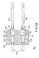
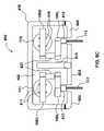
- the optical block 102includes lenses 120 – 123 and reflectors 124 – 125 .
- Lenses 120 – 123may be any collimating lenses including aspheric lenses, ball lenses, and GRIN lenses.
- Lenses 121 – 123may be symmetric (circular symmetry) or asymmetric to provide optical steering.
- Lens 123is for collimating the light or photons diverging from the transmitter 110 and lens 122 is for focussing the collimated light or photons into an optical fiber.
- Lens 120is for collimating the light or photons diverging out from the end of an optical fiber and lens 121 is for focusing the collimated light or photons into the receiver 111 .
- Reflectors 124 – 125may be facets formed in the optical block having angles to provide total internal reflection between the optical block material and the atmosphere. Preferably they are forty five degree angle facets. Alternatively, they may be facets coated with a reflective surface or mirror surface to reflect light or photons off the reflective coated surface or facets having an optical grating surface to reflect photons.
- the optical block 102is preferably constructed of a thermoplastic or polycarbonate which is clear to the desired wavelengths of light or photons.
- the reflectors 124 – 125 , lenses 120 – 123 and other elements of the optical block 102 described beloware preferably formed through injection molding of the desired material.
- Transmitter 110is inserted into an opening 214 in the optical block 102 .
- Receiver 111is inserted into an opening 213 in optical block 102 .
- An epoxyis injected into top and bottom tacking holes 215 in order to hold the transmitter 110 and receiver 111 in openings 214 and 213 respectively.
- An MT alignment plate 201has optical block alignment holes 216 , an optical opening 217 and fiber optic connector alignment pins 218 for alignment purposes.
- the optical block holes 216couple to optical block alignment pins in the optical block 102 , not illustrated in FIG. 2 .
- the fiber optic connector alignment pins 218are for aligning optical fibers that couple to the fiber optic module 100 .
- the fiber optic module 100has a nose 202 and a nose shield 203 .
- the nose 202includes an optical fiber opening 222 and a latch opening 223 .
- the latch opening 223receives the optical fiber connector and holds the optical fiber substantially fixed in place and aligned with the optical opening 217 of the alignment plate 201 .
- the nose shield 203includes an opening 224 for insertion over the nose 202 and shield tabs 225 for coupling to the ground plane of the package.
- the nose shielding 203further reduces EMI.
- the transmitter 110 and receiver 111may be aligned to provide optimal light or photon output and reception. Alignment of the transmitter 110 and receiver 111 in optical block 102 is performed by active alignment where the receiver 111 and transmitter 110 are powered up to detect and emit photons. The receiver 111 and transmitter 110 are properly aligned in the optical block 102 to provide maximum photon detection from or coupling into fiber 101 .
- the tacking holes 215extend into the openings 213 and 214 such that epoxy may poured in to hold the optoelectronic devices to the optical block. After alignment is complete, the epoxy is UV cured and allowed to set such that the receiver 111 and transmitter 110 are substantially coupled to the optical block 102 .
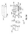
- the receive PCB 108 and the transmit PCB 106may be attached to the receiver 111 and transmitter 110 respectively.
- Receiver thruholes 232 in the receive PCB 108are aligned and slid over terminals 211 of the receiver 111 .
- the terminals 211are then soldered to make an electrical connection on the component side (opposite the side of the ground plane 118 ) of the receive PCB 108 .
- Transmitter thruholes 233 in the transmit PCB 106are aligned and then slid over the terminals 210 of the transmitter 110 .
- the terminals 210are then soldered to make an electrical connection on the component side (opposite the side of the ground plane 114 ) of transmit PCB 106 .
- Ground planes 114 and 118have sufficient material removed around the transmitter thruholes 233 and the receiver thruholes 232 respectively to avoid shorting the terminals of the transmitter 110 and receiver 111 to ground.
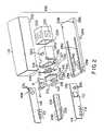
- the assemblyis inserted into the shielded housing or cover 119 .
- the optional internal shield 109is next assembled into the shielded housing or cover 119 between the PCBs 106 and 108 .
- the optional internal shield 109has pin slots 230 to surround the pins 113 and 117 and avoid shorting thereto.
- the shielded housing or cover 119includes clips or tabs 236 at each corner for mating to a base 205 .
- the base 205includes PCB slots 240 , clip openings or slots 238 into which the clips or tabs 236 may be inserted, and base pin holes 242 into which the PCB pins 113 and 117 may be inserted.
- the base 205includes a guide post 244 for mounting the fiber optic module into a system printed circuit board. The bottom of the base mounts parallel to the printed circuit board of the system such that when horizontal, the receive PCB 108 and the transmit PCB 106 are vertical and substantially perpendicular in reference to the printed circuit board of the system and the base 205 .
- the base 205has its base pin holes 242 slid over the PCB pins 113 and 117 , the printed circuit boards 106 and 108 are guided to mate with the PCB slots 240 , and the clips or tabs 236 of the shielded housing or cover 119 are guided into the clip openings or slots 238 .
- the receive PCB pins 113 and the transmit PCB pins 117are vertical and substantially perpendicular in reference to the printed circuit board of the system and the base 205 .
- the clips or tabs 236are bent, twisted, or otherwise changed in order to hold the base 205 in place.
- the shielded housing or cover 119may use plastic clips, or a ridge, integrated into each side that couples to base 205 appropriately.
- the shielded housing or cover 119which is coupled to ground, encases the PCBs 106 and 108 to reduce the electromagnetic fields generated by the electrical components coupled thereto by shunting the electric fields to ground to reduce electromagnetic interference (EMI).
- EMIelectromagnetic interference
- the transmitter 110 , the receiver 111 , and the MT alignment plate 201are coupled to the optical block 102 .
- the light transmitter 110includes an emitter 302 for generation of light or photons in response to electrical signals from the transmit PCB 106 .
- the light receiver 111includes a detector 304 to receive light or photons and generate electrical signals in response to light or photons coupled thereto.
- Light or photons emitted by the emitter 302are coupled into lens 123 and collimated onto the reflector 125 at an incident angle I 1 (angle with the perpendicular to reflector 125 surface) preferably of substantially forty five degrees.
- Reflector 125reflects the incident light or photons on a refraction angle R 1 (angle with the perpendicular to reflector 125 surface) equivalent to incident angle I 1 preferably of substantially forty five degrees.
- the reflected light or photonspreferably travel perpendicular to the incident light or photons towards the lens 122 .
- Lens 122focuses the light or photons from the emitter 302 into an aligned optical fiber through the optical port 217 in the MT alignment plate 201 .
- light or photons coupled or launched into an optical fiber, defining a first optical axisare preferably substantially perpendicular to the light or photons emitted and incident upon lens 123 from the emitter 302 of the transmitter 110 .
- Lens 120collimates the incident light or photons from a fiber optic cable onto the reflector 124 at an incident angle I 2 of preferably substantially forty five degrees.
- Reflector 124reflects incident light or photons at a refractive angle R 2 equivalent to incident angle I 2 of preferably substantially forty five degrees towards lens 121 .
- Lens 121focuses the light or photons received from a fiber optical cable onto the detector 304 .
- Light or photons incident from a fiber optic cable, defining a second optical axis,are preferably substantially perpendicular to the light or photons incident upon the detector 304 .
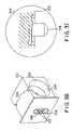
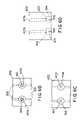
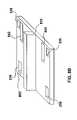
- FIG. 3Billustrates a frontal perspective view from the left side of the optical block 102 .
- the front side of the optical block 102includes optical block alignment pins 316 and an optical output opening 317 .
- the optical block alignment pins 316couple to the alignment holes 216 of the alignment plate 201 such that the optical output opening 317 is aligned with the optical port 217 in the alignment plate 201 .
- FIG. 3Cillustrates the front side of the optical block 102 .
- the optical output opening 317is indicated.
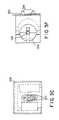
- FIG. 3Dis a back side perspective view from the right of the optical block 102 .
- the back side of the optical block 102includes a cavity 322 that is used to form the shape of the reflective surfaces 124 – 125 during manufacturing of the optical block 102 .
- FIG. 3Eis a back view of the optic block illustrating the opening into the cavity 322 .
- FIG. 3Fillustrates the right side of the optical block 102 which has the opening 214 to mate with the type of housing of the transmitter 110 .
- the lens 123can be viewed near the center of the opening 214 .
- FIG. 3Gillustrates the left side of the optical block 102 . which has the opening 213 to mate with the type of housing of the receiver 111 .
- the lens 121can be viewed near the center of the opening 213 . Comparing FIGS. 3F and 3G , the offset between openings 213 and 214 to avoid optical crosstalk is visible.
- receiver 111is closer to the optical opening 317 in order to minimize the loss of incoming received optical power. However, the position of receiver 111 and transmitter 110 can be interchanged.
- FIG. 3Gillustrates the right side of the optical block 102 which has the opening 214 to mate with the type of housing of the transmitter 110 .
- the lens 123can be viewed near the center of the opening 214 .
- FIG. 3Gillustrates the left
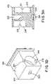
- FIG. 3His a cross-sectional view of the optical block 102 illustrating the relative position of the optical block alignment posts 316 .
- the area 324 surrounding the alignment post 316is magnified in FIG. 3I .
- FIG. 3Iprovides a magnified cross-sectional view of the alignment post 316 .
- FIG. 4illustrates another embodiment of the invention.
- a fiber optic module 400includes an optical block 402 and electrical elements 404 .
- the optical block 402may also be referred to as a nose, an optical port, an alignment block, an optical connector, an optical receptacle or receptacle.
- the optical block 402can interface to an optical connector such as an LC, MT-RJ or VF-45 optical connector.
- Electrical elements 404include transmitter PCB 106 , receiver PCB 108 , light receiver 111 , light transmitter 110 , and a shielded housing or cover 419 .
- Shielded housing or cover 419may be narrower than shielded housing or cover 119 due to receiver 111 and transmitter 110 being parallel with the PCBs 108 and 106 .
- the optical or alignment block 402may include lens 423 and lens 421 for coupling light or photons into and out of the fiber optic cable 101 .
- the lens 423 and 421may be coupled to the receiver 111 and transmitter 110 .
- Lens 423 and 421may be spherical lenses or each may be a pair of aspheric lenses on the same optical axis.
- Light or photons emitted by the transmitter 110are collected and focused by lens 423 into a transmit fiber optic cable.
- Light or photons on a receive fiber optic cableare collected and focused by lens 421 into the receiver 111 .
- fiber optic module 400preferably keeps light or photons substantially in parallel and does not have to reflect the light or photons to couple it with receiver 111 or transmitter 110 .
- FIG. 5Aillustrates an exploded diagram of the fiber optic module 400 .
- Fiber optic module 400is assembled similar to fiber optic module 100 as previously described with reference to FIG. 2 .
- optical or alignment block 402differs from optical block 102 .
- Receiver 111 and transmitter 110are inserted into openings 513 and 514 respectively in the optical or alignment block 402 .
- the receiver and transmittermay be held in place by a press fit or glued in place.
- an epoxy or glueis injected in top and bottom tacking holes 515 of the optical or alignment block 402 while the receiver 111 and transmitter 110 are tested and aligned to substantially couple light or photons into and out of fiber optic cables.
- the transmit PCB 106 and the receive PCB 108are coupled respectively to the transmitter 110 and the receiver 111 .
- the terminals 511 and 510 of the receiver 111 and the transmitter 110respectively are soldered directly onto the PCB.
- the high frequency pins associated with the receiver 111 and transmitter 110are preferably soldered on the component side of the printed circuit boards in order to provide proper shielding.
- the alignment plate 201 , the nose 202 and the nose shielding 203are unnecessary in this embodiment of the invention. Fiber ferrules are utilized instead for alignment between the optical or alignment block 402 and the optical fibers 101 .
- Fiber optic module 400 ′is assembled similar to fiber optic module 400 as previously described with reference to FIG. 5A but a different base 205 ′ is utilized.
- the base 205 ′differs from base 205 in that it has a pair of guide rails 540 to hold the PCBs 106 and 108 in place and a pair of cutouts or open slots 542 for the pins 113 and 117 to extend through. In this manner, the PCBs 106 and 108 may slide into place onto the base 205 ′.
- Fiber optic module 400 ′′is assembled similar to fiber optic module 400 as previously described with reference to FIG. 5A but a different base 205 ′′ is utilized.
- the base 205 ′′differs from base 205 in that it has pairs of mounting brackets 540 ′ to hold the PCBs 106 and 108 in place and a pair of openings 542 ′ for the pins 113 and 117 to extend through.
- FIG. 5Dillustrates an exploded view of a fiber optic module 400 ′′′.
- Fiber optic module 400 ′′′is assembled similar to fiber optic module 400 as previously described with reference to FIG. 5A but a different base 205 ′′′ is utilized and a slightly different optical block 502 is utilized.
- the base 205 ′′′differs from base 205 in that there are no slots 240 and that there are a pair of cutouts or open slots 542 for the pins 113 and 117 to extend through.
- the optical block 502differs from the optical block 402 in that a pair of slots 525 are provided to align the PCBs 106 and 108 with the optical block.
- the transmitter 110 and the receiver 111are coupled to the optical or alignment block 402 .
- the transmitter 110includes an emitter 302 for generation of light or photons.
- the receiver 111includes a detector 304 to receive light or photons.
- Light or photons emitted by the emitter 302are coupled into lens 423 , collected and focused into the optical fiber through the optical port 417 A.
- Light or photons, incident from a fiber optic cable coupled to the fiber optic module 400is received through the optical port 417 B. Photons from the fiber optic cable are incident upon the lens 421 .
- Lens 421collects and focuses the incident light or photons from the fiber optic cable onto the detector 304 of the receiver 111 .
- a pair of fiber ferrules 421are provided. The fiber ferrules 421 are inserted into the optical ports 417 A and 417 B.
- FIG. 6Billustrates the front side of the optical or alignment block 402 .
- the front side of the optical or alignment block 402includes optical output ports 417 A and 417 B.
- the lens 421is visible through the optical output port 417 B and lens 423 is visible through the optical output port 417 A.
- FIG. 6Cis an illustration of the back side of the optical or alignment block 402 .
- the lens 421is visible through opening 513 and lens 423 is visible through opening 514 .
- FIG. 6Dillustrates the top side of the optical or alignment block 402 which has the tacking holes 515 coupling to the openings 513 and 514 . Epoxy may be inserted into the top and bottom tacking holes 515 to hold the transmitter 110 and receiver 111 in position in the optical or alignment block 402 .
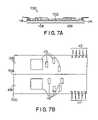
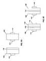
- Transmit PCB 106 and receive PCB 108are assembled as one unit on one printed circuit board 700 with a center score 702 defining a boundary line between transmit and receive components. After all components have been attached and assembled onto the unitary PCB 700 , the PCB 700 is flexed along the score 702 such that the transmit PCB 106 and the receive PCB 108 may be separated. Transmit PCB 106 and the receive PCB 108 may thereafter be assembled as part of the fiber optic module 100 and the fiber optic module 400 .
- the transmit PCB 106 and the receive PCB 108may each be approximately 6.5 mm in height excluding pins 113 and 117 .
- FIG. 8Aillustrates an exploded view of a fiber optic module 800 .
- the fiber optic module 800includes an upper transmit PCB 106 U, a lower transmit PCB 106 L, an upper receive PCB 108 U, a lower receive PCB 108 L, the transmitter 110 , the receiver 111 , the optical block 402 , the shielded housing or cover 419 , a first and second PCB interconnect pin headers 827 , a first terminal pin header 813 for the transmitter, a second terminal pin header 817 for the receiver, and a baseplate 805 .
- the transmitter 110is a transmit optical subassembly (Tx OSA) that includes a VCSEL or other semiconductor device that transduces electrical signals into photons or a light output.
- the receiver 111is a receive optical subassembly (Rx OSA) including a PIN diode or other device that converts photons or light input into electrical signals.
- the Tx OSA and Rx OSAare attached to physically separated transmit and receive electrical subassemblies (ESA's).
- the transmit ESAincludes an upper and lower transmit PCBs 106 U and 106 L with components 116 mounted thereto.
- the receive ESAincludes an upper and lower receive PCBs 108 U and 108 L with components 112 mounted thereto.
- the lower transmit PCB 106 L and the upper transmit PCB 106 Uprovide similar functionality to that of the transmit PCB 106 and include components 112 .
- the lower receive PCB 108 L and the upper receive PCB 108 Uprovide similar functionality to that of the receive PCB 108 and include components 116 .
- the upper and lower transmit PCBs 106 U and 106 Lare parallel to each other in a horizontal plane and parallel with the optical axis of the transmitter 110 .
- the upper and lower receive PCBs 108 U and 108 Lare parallel to each other in a horizontal plane and parallel with the optical axis of the receiver 111 .
- This configuration of parallel horizontal boards for each of the transmit and receive capabilitycan be referred to as dual-stack horizontal modular PCBs.
- the first and second pin interconnect headers 827include the conductive signal pins 837 molded into a non-conductive medium.
- the first and second pin interconnect headers 827are used to interconnect lower and upper PCB's.
- the first pin header 827provides signal interconnection between the upper and lower transmit PCBs 106 U and 106 L.
- the first pin header 827provides signal interconnection between the upper and lower transmit PCBs 106 U and 106 L.
- the second pin header 827provides signal interconnection between the upper and lower receive PCBs 108 U and 108 L.
- the second pin header 827has pins 837 that couple into upper throughholes 847 U in the upper receive PCB 108 U and lower through holes 847 L in the lower receive PCB 108 L.
- the first pin header 827similarly has pins 837 that couple into upper and lower throughholes in the upper and lower transmit PCBs 106 U and 106 L respectively.
- the first and second terminal pin headers 817 and 813include conductive signal pins molded into a non-conductive medium.
- the first and second terminal pin headers 817 and 813are used to route electrical signals to and from the fiber optic module 800 to a host system.
- the first terminal pin header 813has pins 113 that couple to through holes 842 in the lower transmit PCB 106 L.
- the second terminal pin header 817has pins 117 that couple to through holes 842 in the lower receive PCB 108 L.
- the transmitter 110couples to the upper transmit PCB 106 U in one embodiment.
- the terminals 810 of the transmitter 110couple to the upper transmit PCB 106 U in one embodiment.
- one or more terminalscouple to upper edge traces 820 U on a top side of the upper transmit PCB 106 U and one or more terminals couple to lower edge traces 820 L on a back side of the upper transmit PCB 106 U.
- the optoelectronic devicei.e. the transmitter 110 or the receiver 111
- the terminals 810may couple to the lower transmit PCB 106 U.
- the terminals 810may couple between the upper and lower receive PCBs so that one or more couple to the upper PCB and one or more couple to the lower PCB.
- the terminals 810may couple into holes of the upper or lower transmit PCBs or both upper and lower transmit PCBs.
- the optoelectronic devicei.e. the transmitter 110 or the receiver 111
- the optoelectronic devicehas its optical axis nearly parallel with a plane of the printed circuit board.
- the receiver 111couples to the upper receive PCB 108 U in one embodiment.
- the terminals 811 of the receiver 111couple to the upper receive PCB 108 U in one embodiment.
- one or more terminalscouple to upper edge traces 821 U on a top side of the upper receive PCB 108 U and one or more terminals couple to lower edge traces 821 L on a back side of the upper receive PCB 108 U.
- the terminals 811may couple to the lower receive PCB 108 U.
- the terminals 811may couple between the upper and lower receive PCBs so that one or more couple to the upper PCB and one or more couple to the lower PCB.
- the terminals 811may couple into holes of the upper or lower receive PCBs or both upper and lower receive PCBs.
- the baseplate 805may include an inner septum 815 that divides the transceiver and receiver into two separate cavities, for EMI and electrical isolation of the transmitter from the receiver or between channels.
- the baseplate 805acts like a chassis or frame to provide support for the shielded housing or cover 419 and the receiver and transmit subassemblies.
- the baseplate 805may include an inner septum 815 , one or more openings 242 to receive the pins 113 and 117 , and one or more clip openings or slots 238 to receive the clips or tabs 236 .
- the baseplate 805in one embodiment is plastic in other embodiments that baseplate may be metal or a metalized plastic to provide shielding.
- the inner septum 815provides separation between the transmitter and the receiver or between channels.
- Baseplate 805 ′differs from baseplate 805 in that it includes slots 842 for pins 113 and 117 .
- Baseplate 805 ′may similarly include clip openings or slots 238 and the inner septum 815 .
- the baseplate 805 with the inner septum 815can divide the fiber optic module 800 into two separate cavities.
- the separate cavitiescan improve EMI and electrical isolation of the transmitter from the receiver.
- the receiver 111couples to the upper receive PCB 108 U with its terminals 811 using a straddle mount in one embodiment.
- the transmitter 111couples to the upper transmit PCB 106 U with its terminals 810 using a straddle mount in one embodiment.
- the upper and lower transmit PCBs 106 U and 106 Lare parallel to each other in a horizontal plane and parallel with the optical axis of the transmitter 110 .
- the upper and lower receive PCBs 108 U and 108 Lare parallel to each other in a horizontal plane and parallel with the optical axis of the receiver 111 .
- This configuration of parallel horizontal boards for each channelcan be referred to as dual-stack horizontal modular PCBs.
- the dual stacked horizontal PCB'sallow an increase in component surface mounting area for a given volume. Both sides of the upper and lower transmit and receive PCB's can be utilized to mount electronic components. This increased surface area can provide increased functionality in a fiber optic module by allowing additional components such as integrated circuits and passive components such as filters, capacitors, and inductors to be utilized.
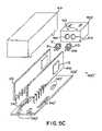
- FIG. 9Aillustrates an exploded view of a fiber optic module 900 .
- the fiber optic module 900utilizes a motherboard which is common to daughtercards PCBs which are substantially perpendicular to the motherboard. Assuming the motherboard is horizontal, the daughtercard PCBs are substantially vertical to the motherboard and can be also be referred to as vertical PCBs. The substantially vertical PCB's couple to the common motherboard.
- the fiber optic module 900includes a vertical transmit PCB 106 ′ and a vertical receive PCB 108 ′ in parallel coupled to a horizontal motherboard PCB 905 .
- the motherboard PCB 905can separate ground and power planes between receiver and transmitter channels in order to maximize isolation and minimize cross talk.
- the vertical transmit PCB and the vertical receive PCBmay have traces soldered to traces of the motherboard for electrical connectivity or otherwise include pins that plugged into holes or sockets of the motherboard to ease replacement or to expand the number of transmit or receive channels with additional transmit PCBs or receive PCBs.
- the electrical connection between the vertical transmit PCB and the vertical receive PCB and motherboard PCBmay be made with electrical connectors in lieu of solder joints.
- the mother board PCBincludes Input/Output Pins (I/O Pins) or an I/O socket connector to couple to holes or a socket of a host system PCB to interface with a host system.
- the vertical transmit PCB and the vertical receive PCBprovides mounting surfaces for components on both the left and right side surfaces (or front and back surfaces). Additionally, a top surface of the motherboard PCB 905 may also be used to mount components or circuits for increased electrical functionality such as a clock/data recovery (CDR) function and minimize the form factor of the fiber optic module.
- CDRclock/data recovery
- an inner shield similar to the shield 109may be used.
- one or both of the vertical transmit PCB and the vertical receive PCBmay have a ground plane on of its left or right side surfaces (sometimes referred to as a backside ground plane).
- the vertical PCBs 106 ′ and 108 ′are similar to PCBs 106 and 108 but for the coupling to the horizontal motherboard PCB 905 .
- the vertical PCBs 106 ′ and 108 ′have signal traces soldered to signal traces of the horizontal motherboard PCB 905 which can also mechanically support the vertical PCBs 106 ′ and 108 ′.
- Solder joints 917 Rcouple the receive PCB 108 ′ to the horizontal motherboard PCB 905 .
- Solder joints 917 Tcouple the transmit PCB 106 ′ to the horizontal motherboard PCB 905 (see FIG. 9B ).
- the fiber optic module 900can be referred to as having vertical PCB's with a horizontal motherboard PCB.
- the horizontal motherboard PCB 905includes input/output (I/O) pins 113 and 117 to couple to a host system and wire traces to route power, ground and signals between the pins 113 and 117 and the vertical PCBs 106 ′ and 108 ′.
- I/Oinput/output
- the fiber optic module 900further includes the transmitter 110 , the receiver 111 , the optical block 402 , and the shielded housing or cover 419 .
- the shielded housing or cover 419has clips or tabs 236 that couple into clip openings or slots 238 in the motherboard PCB 905 .
- the clips or tabs 236can be held in place in the slots by a friction fit or glued in place or they may extend through the motherboard PCB 905 and be turned and or bent to couple the shielded housing or cover 419 and the motherboard PCB 905 together.
- the clips or tabs 236 of the shielded housing or cover 419can wrap around the motherboard PCB 905 to couple them together.
- the transmitter 110couples into the opening 514 of the optical block 402 .
- the receiver 111couples into the opening 513 of the optical block. They are held in place by either a friction fit or a glue such as an epoxy.
- the transmitter 110couples to the transmit PCB 106 ′.
- the terminals 810 of the transmitter 110couple to the transmit PCB 106 ′.
- one or more terminals 810couple to left edge traces 920 L on a left side and one or more terminals 810 couple to right edge traces 920 R on a right side of the transmit PCB 106 ′.
- the terminals 810may couple to one side of the transmit PCB 106 ′.
- the terminals 810may couple into holes of the transmit PCB 106 ′.
- the receiver 111couples to the receive PCB 108 ′.
- the terminals 811 of the receiver 111couple to the receive PCB 108 ′.
- one or more terminals 811couple to left edge traces 921 L on a left side and one or more terminals 811 couple to right edge traces 921 R on a right side of the receive PCB 108 ′.
- the terminals 811may couple to one side of the receive PCB 108 ′.
- the terminals 811may couple into holes of the receive PCB 108 ′.
- FIG. 9Ba rear cross-sectional view of the assembled fiber optic module 900 is illustrated.
- Traces 920 on the motherboard PCBroute signals to components on the motherboard PCB, the I/O pins 113 and 117 , and the solder joints 917 R and 917 T.
- a ground plane 118can be coupled to a side the vertical receive PCB 108 ′ or a ground plane 114 can be coupled to a side of the vertical transmit PCB 106 ′ or both.
- the vertical transmit PCB 106 ′includes the ground plane 114 and the vertical receive PCB 108 ′ is without a ground plane to allow room for added components 116 on each side; Referring to FIG.
- the vertical receive PCB 108 ′includes the ground plane 118 and the vertical transmit PCB 106 ′ is without a ground plane to allow room for added components 112 on each side.
- An optional inner shield 109can also be used for further isolation between channels to reduce cross-talk and EMI as illustrated in FIG. 9B .
- the ground plane 114 and 118will have cutouts for traces to coupled to the terminals 810 and 811 and may have additional cutouts for components 112 or 116 as the case may be. Referring now to FIG.
- the ground plane 118 or the ground plane 114may be alternatively sandwiched between layers of either the vertical receive PCB 108 ′ or the vertical transmit PCB 106 ′ or both as a part of a multilayer PCB as illustrated by FIG. 9C . This can allow for further components 116 and 112 to be added to both sides of the vertical receive PCB 108 ′ and the vertical transmit PCB 106 ′.
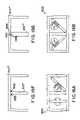
- FIG. 10Aillustrates an exploded view of a fiber optic module 1000 .
- the fiber optic module 1000has angled PCBs with respect to a horizontal or vertical axis of the fiber optic module 1000 .
- the length of the PCBsremain parallel to the optical axis of the receiver 111 and transmitter 110 .
- the PCBsmay be made smaller to fit a smaller form factor or alternatively the surface area can be increased. That is the available PCB surface area for mounting components can be increased for a given volume by angling the PCBs.
- the increased surface areacan give the final assembled fiber optic module increased functionality by allowing components such as integrated circuits and passive components such as filters, capacitors, and inductors to be added. More room can also be provided in the fiber optic module 1000 for mounting larger components by angling the PCBs.
- the fiber optic module 1000includes an angled transmit PCB 106 ′′, an angled receive PCB 108 ′′, the transmitter 110 , the receiver 111 , an optical block 402 ′, the shielded housing or cover 419 , a first terminal pin header 1027 T for the transmitter, a second terminal pin header 1027 R for the receiver, and the baseplate 805 or 805 ′.
- the angled transmit PCB 106 ′′ and the angled receive PCB 108 ′′are arranged within the fiber optic module at an angle with respect to the horizontal axis thereof as defined by a line normal to both receiver and transmitter optical axes.
- the angled transmit PCB 106 ′′ and the angled receive PCB 108 ′′are held in place having a width that is on an angle with respect to a horizontal or vertical axis of the fiber optic module 1000 .
- the length of the angled transmit PCB 106 ′′ and the angled receive PCB 108 ′′are parallel to the optical axis of the receiver 111 and transmitter 110 .
- the angled transmit PCB 106 ′′includes components 116 and left and right edge traces 921 L and 921 R.
- the first terminal pin header 1027 Thas pins 117 that couple to holes of the angled transmit PCB 106 ′′ on one end.
- the angled receive PCB 108 ′′includes components 112 and left and right edge traces 920 L and 920 R.
- the second terminal pin header 1027 Rhas pins 113 that couple to holes of the angled receive PCB 108 ′′ on one end.
- the transmitter 110is a transmit optical subassembly (Tx OSA) that includes a VCSEL or other semiconductor device that transduces electrical signals into photons or a light output.
- the receiver 111is a receive optical subassembly (Rx OSA) including a PIN diode or other device that converts photons or light input into electrical signals.
- the Tx OSA and Rx OSAare attached to physically separated transmit and receive electrical subassemblies (ESA's).
- the transmit ESAincludes the angled transmit PCB 106 ′′ with components 116 and the first terminal pin header 1027 T mounted thereto.
- the receive ESAincludes the angled receive PCB 108 ′′ with components 112 and the second terminal pin header 1027 R mounted thereto.
- the optical block 402 ′is similar to the optical block 402 but has some modifications to accommodate the angled transmit PCB 106 ′′ and the angled receive PCB 108 ′′.
- the optical block 402 ′includes openings 513 ′ and 514 ′ to receive the receiver 111 and transmitter 110 respectively and angled slots 1015 to receive the angled transmit PCB 106 ′′ and the angled receive PCB 108 ′′.
- the angled slots 1015can provide a friction fit with the angled transmit PCB 106 ′′ and the angled receive PCB 108 ′′ or glue or epoxy can be used to couple them together.
- the angled slots 1015can also serve to tack the receiver 111 and transmitter 110 in place within the optical block 402 ′.
- the transmitter 110couples into the opening 514 ′ of the optical block 402 ′.
- the receiver 111couples into the opening 513 ′ of the optical block 402 ′. They can be held in place by either a friction fit or a glue such as an epoxy.
- the transmitter 110also couples to the transmit PCB 106 ′′.
- the terminals 810 of the transmitter 110couple to the transmit PCB 106 ′′ in one embodiment.
- one or more terminals 810couple to left edge traces 920 L on a left side and one or more terminals 810 couple to right edge traces 920 R on a right side of the transmit PCB 106 ′′.
- the terminals 810may couple to one side of the transmit PCB 106 ′′.
- the terminals 810may couple into holes of the transmit PCB 106 ′′.
- the receiver 111also couples to the receive PCB 108 ′′.
- the terminals 811 of the receiver 111couple to the receive PCB 108 ′′.
- one or more terminals 811couple to left edge traces 921 L on a left side and one or more terminals 811 couple to right edge traces 921 R on a right side of the receive PCB 108 ′′.
- the terminals 811may couple to one side of the receive PCB 108 ′′.
- the terminals 811may couple into holes of the receive PCB 108 ′′.
- the first terminal pin header 1027 Tis coupled to the angled transmit PCB 1027 T so that pins 117 are vertical with the reference axis.
- the second terminal pin header 1027 Ris coupled to the angled receive PCB 108 ′′ so that pins 113 are vertical with the reference axis.
- a ground plane 118can be coupled to a side the angled receive PCB 108 ′′ or a ground plane 114 can be coupled to a side of the angled transmit PCB 106 ′′ or both similar to previously described with reference to the vertical boards and FIGS. 9B–9E .
- the shield housing or cover 419couples to the base or baseplate 805 or 805 ′ around the printed circuit boards.
- the angles ⁇ 1 and ⁇ 2 which the printed boards make with the base or baseplate 805 or 805 ′can vary between zero and ninety degrees.
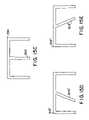
- FIG. 11Aillustrates an exploded view of a fiber optic module 1100 .
- the fiber optic module 1100has parallel angled or slanted PCBs with respect to a horizontal or vertical axis of the fiber optic module 1100 .
- the length of the PCBsremain parallel to the optical axis of the receiver 111 and transmitter 110 .
- the PCBsmay be made smaller to fit a smaller form factor or alternatively the surface area can be increased. That is the available PCB surface area for mounting components can be increased for a given volume by angling the PCBs.
- the increased surface areacan give the final assembled fiber optic module increased functionality by allowing components such as integrated circuits and passive components such as filters, capacitors, and inductors to be added. More room can also be provided in the fiber optic module 1100 for mounting larger components by angling the PCBs in parallel together.
- the fiber optic module 1100includes an angled transmit PCB 106 ′′′, an angled receive PCB 108 ′′′, the transmitter 110 , the receiver 111 , an optical block 402 ′′, the shielded housing or cover 419 , a first terminal pin header 1027 T′ for the transmitter, a second terminal pin header 1027 R′ for the receiver, and a baseplate 805 ′′.
- the angled transmit PCB 106 ′′′ and the angled receive PCB 108 ′′′are arranged in parallel and at an angle with respect to a horizontal datum plane that passes through and is normal to receiver and transmitter optical axes.
- the angled transmit PCB 106 ′′′ and the angled receive PCB 108 ′′′are slanted in parallel to the right but can be easily arranged so as to slant in parallel to the left.
- the angled transmit PCB 106 ′′′ and the angled receive PCB 108 ′′′are held in place having a width that is on an angle with respect to a horizontal or vertical axis of the fiber optic module 1100 .
- the length of the angled transmit PCB 106 ′′′ and the angled receive PCB 108 ′′′are parallel to the optical axis of the receiver 111 and transmitter 110 .
- the angled transmit PCB 106 ′′′includes components 116 and left and right edge traces 921 L and 921 R.
- the first terminal pin header 1027 T′has pins 117 that couple to holes of the angled transmit PCB 106 ′′′ on one end.
- the angled receive PCB 108 ′′′includes components 112 and left and right edge traces 920 L and 920 R.
- the second terminal pin header 1027 R′has pins 113 that couple to holes of the angled receive PCB 108 ′′′ on one end.
- the transmitter 110is a transmit optical subassembly (Tx OSA) that includes a VCSEL or other semiconductor device that transduces electrical signals into photons or a light output.
- the receiver 111is a receive optical subassembly (Rx OSA) including a PIN diode or other device that converts photons or light input into electrical signals.
- the Tx OSA and Rx OSAare attached to physically separated transmit and receive electrical subassemblies (ESA's).
- the transmit ESAincludes the angled transmit PCB 106 ′′′ with components 116 and the first terminal pin header 1027 T′ mounted thereto.
- the receive ESAincludes the angled receive PCB 108 ′′′ with components 112 and the second terminal pin header 1027 R′ mounted thereto.
- the baseplate 805 ′′is similar to the baseplate 805 and 805 ′ but has angled inner septum 815 ′ to be angled in parallel with the angled transmit PCB 106 ′′′ and the angled receive PCB 108 ′′′.
- the baseplates 805 , 805 ′, 805 ′′in one embodiment may be a dielectric to isolate components and insulate them from one another.
- baseplates 805 , 805 ′, 805 ′′may be an insulator.
- baseplates 805 , 805 ′, 805 ′′may have their septum 815 or 815 ′ metalized so as to provide EMI and crosstalk shielding.
- a metal shieldmy be placed on top of the septum 815 or 815 ′ such as shield 109 .
- the optical block 402 ′′is similar to the optical block 402 but has some modifications to accommodate the angled transmit PCB 106 ′′′ and the angled receive PCB 108 ′′′.
- the optical block 402 ′′includes openings 513 ′′ and 514 ′′ to receive the receiver 111 and transmitter 110 respectively and angled slots 1115 to receive the angled transmit PCB 106 ′′′ and the angled receive PCB 108 ′′′.
- the angled slots 1115can provide a friction fit with the angled transmit PCB 106 ′′′ and the angled receive PCB 108 ′′′ or glue or epoxy can be used to couple them together.
- the angled slots 1115can also serve to tack the receiver 111 and transmitter 110 in place within the optical block 402 ′′.
- the transmitter 110couples into the opening 514 ′′ of the optical block 402 ′′.
- the receiver 111couples into the opening 513 ′′ of the optical block 402 ′′. They can be held in place by either a friction fit or a glue such as an epoxy.
- the transmitter 110also couples to the transmit PCB 106 ′′′.
- the terminals 810 of the transmitter 110couple to the transmit PCB 106 ′′′ in one embodiment.
- one or more terminals 810couple to left edge traces 920 L on a left side and one or more terminals 810 couple to right edge traces 920 R on a right side of the transmit PCB 106 ′′′.
- the terminals 810may couple to one side of the transmit PCB 106 ′′′.
- the terminals 810may couple into holes of the transmit PCB 106 ′′′.
- the receiver 111also couples to the receive PCB 108 ′′′.
- the terminals 811 of the receiver 111couple to the receive PCB 108 ′′′.
- one or more terminals 811couple to left edge traces 921 L on a left side and one or more terminals 811 couple to right edge traces 921 R on a right side of the receive PCB 108 ′′′.
- the terminals 811may couple to one side of the receive PCB 108 ′′′.
- the terminals 811may couple into holes of the receive PCB 108 ′′′.
- FIG. 11Ba rear cross-sectional view of the assembled fiber optic module 1100 is illustrated.
- the angled receive PCB 108 ′′′ and the angled transmit PCB 106 ′′′ of the fiber optic module 1100are angled in parallel together with respect to a horizontal or vertical axis thereof.
- the first terminal pin header 1027 T′is coupled to the angled transmit PCB 1027 T′ so that pins 117 are vertical with the reference axis.
- the second terminal pin header 1027 R′is coupled to the angled receive PCB 108 ′′′ so that pins 113 are vertical with the reference axis.
- a ground plane 118can be coupled to a side the angled receive PCB 108 ′′′ or a ground plane 114 can be coupled to a side of the angled transmit PCB 106 ′′′ or both similar to previously described with reference to the vertical boards and FIGS. 9B–9E .
- the shield housing or cover 419couples to the baseplate 805 ′′ around the printed circuit boards.
- the angles ⁇ 3 and ⁇ 4 which the printed boards make with the base or baseplate 805 ′′ and the angle ⁇ 5 which the septum 815 ′ makes with the base or baseplate 805 ′′can vary between zero and ninety degrees.
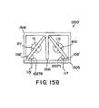
- FIG. 12Aillustrates an exploded view of a fiber optic module 1200 .
- the fiber optic module 1200has angled or slanted PCBs with respect to a horizontal or vertical axis of the fiber optic module 1200 .
- the PCBsare angled or slanted away at top edges to form a V configuration of PCB orientation.
- the length of the PCBsremain parallel to the optical axis of the receiver 111 and transmitter 110 .
- the PCBsmay be made smaller to fit a smaller form factor or alternatively the surface area can be increased.
- the available PCB surface area for mounting componentscan be increased for a given volume by angling the PCBs.
- the increased surface areacan give the final assembled fiber optic module increased functionality by allowing components such as integrated circuits and passive components such as filters, capacitors, and inductors to be added. More room can also be provided in the fiber optic module 1200 for mounting larger components by angling the PCBs.
- the fiber optic module 1200includes an angled transmit PCB 106 ′′′′, an angled receive PCB 108 ′′′′, the transmitter 110 , the receiver 111 , an optical block 402 ′′′, the shielded housing or cover 419 , a first terminal pin header 1027 T′′ for the transmitter, a second terminal pin header 1027 R′′ for the receiver, and the baseplate 805 or 805 ′.
- the angled transmit PCB 106 ′′′′ and the angled receive PCB 108 ′′′′are arranged at an angle with respect to the horizontal axis of the fiber optic module as defined by a line normal to both receiver and transmitter optical axes.
- the angled transmit PCB 106 ′′′′ and the angled receive PCB 108 ′′′′slant away from each other to form the V configuration.
- the angled transmit PCB 106 ′′′′ and the angled receive PCB 108 ′′′′are held in place having a width that is on an angle with respect to a horizontal or vertical axis of the fiber optic module 1200 .
- the length of the angled transmit PCB 106 ′′′′ and the angled receive PCB 108 ′′′′are parallel to the optical axis of the receiver 111 and transmitter 110 .
- the angled transmit PCB 106 ′′′′includes components 116 and left and right edge traces 921 L and 921 R.
- the first terminal pin header 1027 T′′has pins 117 that couple to holes of the angled transmit PCB 106 ′′′′ on one end.
- the angled receive PCB 108 ′′′′includes components 112 and left and right edge traces 920 L and 920 R.
- the second terminal pin header 1027 R′′has pins 113 that couple to holes of the angled receive PCB 108 ′′′′ on one end.
- the transmitter 110is a transmit optical subassembly (Tx OSA) that includes a VCSEL or other semiconductor device that transduces electrical signals into photons or a light output.
- the receiver 111is a receive optical subassembly (Rx OSA) including a PIN diode or other device that converts photons or light input into electrical signals.
- the Tx OSA and Rx OSAare attached to physically separated transmit and receive electrical subassemblies (ESA's).
- the transmit ESAincludes the angled transmit PCB 106 ′′′′ with components 116 and the first terminal pin header 1027 T′′ mounted thereto.
- the receive ESAincludes the angled receive PCB 108 ′′′′ with components 112 and the second terminal pin header 1027 R′′ mounted thereto.
- the optical block 402 ′′′is similar to the optical block 402 but has some modifications to accommodate the angled transmit PCB 106 ′′′′ and the angled receive PCB 108 ′′′′.
- the optical block 402 ′′′includes openings 513 ′′′ and 514 ′′′ to receive the receiver 111 and transmitter 110 respectively and angled slots 1215 to receive the angled transmit PCB 106 ′′′′ and the angled receive PCB 108 ′′′′.
- the angled slots 1215can provide a friction fit with the angled transmit PCB 106 ′′′′ and the angled receive PCB 108 ′′′′ or glue or epoxy can be used to couple them together.
- the angled slots 1215can also serve to tack the receiver 111 and transmitter 110 in place within the optical block 402 ′′′.
- the transmitter 110couples into the opening 514 ′′′ of the optical block 402 ′′′.
- the receiver 111couples into the opening 513 ′′′ of the optical block 402 ′′′. They can be held in place by either a friction fit or a glue such as an epoxy.
- the transmitter 110also couples to the transmit PCB 106 ′′′′.
- the terminals 810 of the transmitter 110couple to the transmit PCB 106 ′′′′ in one embodiment.
- one or more terminals 810couple to left edge traces 920 L on a left side and one or more terminals 810 couple to right edge traces 920 R on a right side of the transmit PCB 106 ′′′′.
- the terminals 810may couple to one side of the transmit PCB 106 ′′′′.
- the terminals 810may couple into holes of the transmit PCB 106 ′′′′.
- the receiver 111also couples to the receive PCB 108 ′′′′.
- the terminals 811 of the receiver 111couple to the receive PCB 108 ′′′′.
- one or more terminals 811couple to left edge traces 921 L on a left side and one or more terminals 811 couple to right edge traces 921 R on a right side of the receive PCB 108 ′′′′.
- the terminals 811may couple to one side of the receive PCB 108 ′′′′.
- the terminals 811may couple into holes of the receive PCB 108 ′′′′.
- FIG. 12Ba rear cross-sectional view of the assembled fiber optic module 1200 is illustrated.
- the angled receive PCB 108 ′′′′ and the angled transmit PCB 106 ′′′′ of the fiber optic module 1200are angled away from each other with respect to a horizontal or vertical axis thereof.
- the first terminal pin header 1027 T′′is coupled to the angled transmit PCB 1027 T′′ so that pins 117 are vertical with the reference axis.
- the second terminal pin header 1027 R′′is coupled to the angled receive PCB 108 ′′′′ so that pins 113 are vertical with the reference axis.
- a ground plane 118can be coupled to a side the angled receive PCB 108 ′′′′ or a ground plane 114 can be coupled to a side of the angled transmit PCB 106 ′′′′ or both similar to previously described with reference to the vertical boards and FIGS. 9B–9E .
- the shield housing or cover 419couples to the baseplate 805 or 805 ′ around the printed circuit boards.
- the angles ⁇ 6 and ⁇ 7 which the printed boards make with the base or baseplate 805 or 805 ′can vary between zero and ninety degrees.
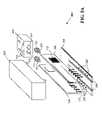
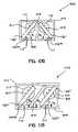
- FIG. 16Aillustrates a fiber optic module 1600 with such an arrangement for an alternate embodiment of the invention.
- a receiver optical block 402 R and a transmitter optical block 402 Tare illustrated as an alternative to the optical block 402 or 402 ′.
- the fiber optic moduleswere described and illustrate using a single optical block 402 or 402 ′.
- the optical blocks 402 R and 402 Tcan provide similar functionality to the single optical block 402 or 402 ′.
- the receiver optical block 402 Rcouples to the receiver 111 while the transmit optical block 402 T couples to the transmitter 110 .
- the receiver 111 and transmitter 110can be press fit into the openings 513 and 514 or alternatively a glue or epoxy can inserted into the tacking holes to couple them together.
- Each optical receiver optical block 402 R and transmit optical block 402 Tprovides alignment to an optical fiber and may include a lens. If one more receiver channels are desired, one or more receiver optical blocks 402 R can be utilized. If one or more transmit channels are desired, one or more transmit optical blocks 402 T can be utilized.
- pins 113 and 117 of the fiber optic modules( 100 , 400 , 800 , 900 , 1000 , 1100 , or 1200 ) facilitate soldering to a host printed circuit board, they can also be plugged into a socket 1402 on a host printed circuit board 1404 as illustrated in FIG. 14A .
- the pins 113 and 117can each be replaced with one or more sockets 1406 R and 1406 T coupled to the printed circuit boards on the bottom edge or back edge.
- the fiber optic module( 100 , 400 , 800 , 900 , 1000 , 1100 , or 1200 ) plugs vertically or downward on sockets 1408 R and 1408 T for example of the host printed circuit board 1404 ′ as illustrated by FIG. 14B .
- the fiber optic module( 100 , 400 , 800 , 900 , 1000 , 1100 , or 1200 ) plugs horizontally or inward into a socket or sockets 1418 R and 1418 T of the host printed circuit board 1404 ′′.
- the shielded housing or cover 1519includes a center inner septum 1515 incorporated as part of the housing or cover to isolate a transmit channel from a receive channel or one channel from another channel.
- the center inner septum 1515splits the fiber optic module into a left side and a right side as does the other septums described herein.
- the housing or cover 1519further includes a back side 1521 , a left side 1522 , a right side 1523 and clips or tabs 236 .
- a front side 1524 of the housing or cover 1519is open to couple to the optical block 402 and/or a nose.
- the alternate base 1505has no septum and may include clip openings or slots 238 .
- a baseis without the clip openings or slots 238 such that the clips or tabs 236 of the housing or cover are bent over and around the base.
- FIG. 15Ba cross sectional view of a fiber optic module 1000 ′ utilizing the alternate embodiment of the shielded housing or cover 1519 and base 1505 is illustrated.
- the fiber optic module 1000 ′is similar to fiber optic module 1000 as described with reference to FIGS. 10A–10B but for the alternate shielded housing or cover 1519 and the alternate base 1505 .
- the shielded housing or cover 1519is a monolithic or integrated shielded housing or cover incorporating the septum 1515 .
- the shielded housing or cover 1519can be formed of a metal, a plastic or other solid material.
- the shielded housing or cover 1519if made of metal, can be formed by forging, stamping or machining. Lower costs methods to fabricate the shielded housing or cover 1519 include injection, transfer, or blow molding the shape out of plastic.
- the plasticcan then be plated, painted or otherwise coated with a conductive material, if conductivity is desired. Likewise a metal part can be overcoated with a non-conductive material if conductivity is not desired.
- the septumcan be angled as well to accommodate parallel angled PCB boards as illustrated by the septum 1515 ′ of the shielded housing or cover 1519 ′ and the septum 1515 ′′ of the shielded housing or cover 1519 ′′.
- the septumcan be formed separately from the housing or cover and coupled thereto.
- the shielded housing or cover 1519 ′′′includes a septum 1515 ′′′ which is formed separately and coupled together.
- the septum 1515 ′′′can be coupled to the outer housing by using fusion techniques such as soldering, welding, or melting.
- FIG. 15Fillustrates the fuse links 1530 (solder, weld, etc) coupling the septum 1515 ′′′ to the outer housing of the shielded housing or cover 1519 ′′′.
- FIG. 15Gillustrates the shielded housing or cover 1519 ′′′′ including a septum 1515 ′′′′ which is formed separately and coupled together.
- the outer cover of the shielded housing or cover 1519 ′′′′includes a groove 1532 and the septum 1515 ′′′′ includes a tongue 1534 to form a tongue and groove system.
- a glue, adhesive or epoxy 1535is applied between the tongue and groove system which may be conductive or non-conductive to couple the outer housing and the septum 1515 ′′′′ together to form the shielded housing or cover 1519 ′′′′.
- the fiber optic modules previously described with reference to FIGS. 8A–15Gwere illustrated with the optoelectronic devices (transmitter 110 and receiver 111 ) having its terminals coupled to the printed circuit boards using a straddle mount. However, one or all of the optoelectronic devices may have their terminals coupled to the printed circuit boards using a through hole mount.
- the optoelectronic devicei.e. the transmitter 110 or the receiver 111
- the optoelectronic deviceIn a straddle mount, the optoelectronic device (i.e. the transmitter 110 or the receiver 111 ) has its optical axis nearly in-line and parallel with a plane of the printed circuit board.
- the optoelectronic devicei.e. the transmitter 110 or the receiver 111
- a rear cross-section of a fiber optic module 1600is illustrated having a first optoelectronic device with its terminals coupled to a first printed circuit board in a straddle mount configuration and a second optoelectronic device with its terminals coupled to a second printed circuit board in a through hole mount configuration.
- both the first optoelectronic device the second optoelectronic devicemay have their terminals coupled to their respective printed circuit boards in a through hole mount configuration as illustrated by the rear cross-section of fiber optic module 1602 of FIG. 16B .
- the pluggable fiber optic module 1700is an MTRJ-SFP pluggable fiber optic module.
- the pluggable fiber optic module 1700may include a cover/housing 1702 , an interface printed circuit board (PCB) 1704 , a support base 1706 , a transmit printed circuit board (PCB) 1708 , a receive printed circuit board (PCB) 1710 , the optical block 102 , the transmitter 110 , the receiver 111 , an alignment plate 201 ′, a nose receptacle 202 ′, and an actuator 1714 .
- PCBinterface printed circuit board
- PCBtransmit printed circuit board
- PCBreceive printed circuit board
- optical block 102The details of the optical block 102 , the transmitter 110 , the receiver 111 were previously described and will not be repeated here for reasons of brevity.
- the cover/housing 1702may have one or more top, left, and right side electromagnetic interference (EMI) fingers 1720 T, 1720 L, 1720 R extending outward from a top surface, left surface and right surface thereof, respectively.
- the cover/housing 1702may further have one or more right and left side openings 1721 R, 1721 L, 1722 R, 1722 L, 1723 R, 1723 L in the top surface, the left surface, and the right surface thereof.
- the cover/housing 1702may further have a contact tab 1726 extending inward from the top surface.
- the right and left side openings 1721 R, 1721 L, 1722 R, 1722 Lmay interface to right and left tabs 1741 R, 1741 L, 1742 R, 1742 L in the support base 1704 to couple the cover/housing 102 to a subassembly of the fiber optic module 1700 .
- the right and left side openings 1723 R, 1723 Lmay interface to right and left tabs (right tab 1782 R only shown in the Figures with left tab 1782 L being a mirror image thereof) in the nose receptacle 202 ′ to further the cover/housing 102 to the subassembly of the fiber optic module 1700 .
- the contact tab 1726may electrically couple to an edge of the alignment plate 201 ′, if its conductive. Alternatively, the contact tab 1726 may extend and electrically couple to both the alignment plate 201 ′ and the nose receptacle 202 ′ if both are conductive.
- the cover/housing 1702 , alignment plate 201 ′, and nose receptacle 202 ′may be formed of a metal or a plastic.
- the plasticmay be metalized to form of a metalized plastic in order to be conductive and provide static (ESD), EMI, or RF shielding through a ground connection which may be made through the one or more fingers 1720 T, 1720 L, 1720 R (one or more fingers 1720 L are not shown in the figures but being a mirror image of the one or more fingers 1720 R).
- the cover/housing 1702is formed of stainless steel.
- the interface PCB 1704may also be referred to as a horizontal printed circuit board.
- the interface PCB 1704may include one or more openings 1734 to slide over one or more alignment pillars 1740 in the support base 1706 .
- the interface PCB 1704may further include an edge connection 1730 formed by traces on the surface of the interface PCB 1704 ; left and right side solder pads 1732 L, 1732 R; and one or more integrated circuits (ICs) 1736 or other electrical components.
- the edge connection 1730 of the interface PCB 1704may also be referred to as an edge connector, a plug, an interface slot, or a connector tongue.
- the left and right side solder pads 1732 L, 1732 Rare for forming an electrical connection with the transmit PCB 1708 and the receive PCB 1710 by means of one or more solder joints.
- each solder jointis a ninety degree castellation solder joint.
- the interface PCB 1704may further include left and right cutouts 1738 L, 1738 R which may allow respective edges of the transmit PCB 1708 and the receive PCB 1710 to slide into respective left and right slots 1743 L, 1743 R in the support base 1706 .
- the edge connection 1730 of the interface PCB 1704allows the fiber optic module 1700 to be plugged into and out of an edge connector of a host printed circuit board.
- the edge connection 1730as discussed further below, may allow for the hot pluggability of the fiber optic module 1700 into a powered up host printed circuit board.
- the support base 1706may include the one or more alignment pillars 1740 ; the left and right tabs 1741 R, 1741 L, 1742 R, 1742 L (left tab 1741 L is not shown in the figures but being a mirror image of the right tab 1741 R); the left and right slots 1743 L, 1743 R; a support edge 1744 ; and a support tab 1746 .
- the left slot 1743 Lis for receiving an edge of the transmit PCB 1708 in the preferred embodiment.
- the right slot 1743 Ris for receiving an edge of the receive PCB 1710 in the preferred embodiment.
- the receive PCB and transmit PCBcan swap sides along with swapping sides of the transmitter 110 and receiver 111 and the optical components (i.e. lenses, etc.) within the optical block 102 .
- the interface PCB 1704may include one or more openings 1734 to slide over the one or more alignment pillars 1740 in the support base 1706 .
- An epoxy or gluecan be deposited around the pillars 1740 and on the surface of the interface PCB 1704 near the openings 1734 in order to hold interface PCB 1704 and the support base 1706 coupled together.
- the edge connection 1730 of the interface PCB 1704is plugged into and out of an edge connector of a host PCB
- the pillars 1740deter movement of the interface PCB 1704 with respect to the fiber optic module 1700 .
- the support edge 1744 of the support base 1706provides support to the interface PCB 1704 nearer the edge connection 1730 .
- the support tab 1746provides support to the interface PCB 1704 near an end opposite to the end having the edge connection 1730 .
- the right and left tabs 1741 R, 1741 L, 1742 R, 1742 L in the support base 1704couple into the right and left side openings 1721 R, 1721 L, 1722 R, 1722 L in the cover/housing 102 to couple the cover/housing 102 and the support base 1704 together.
- the tabsare shaped as a ramp or a wedge as illustrated so that the edges of the cover/housing 102 can easily slide over the tabs.
- the receive PCB 1710may also be referred to as a vertical printed circuit board and is a receiver electrical subassembly.
- the receive PCB 1710includes one or more solder pads 1752 , one or more integrated circuits (ICs) 1754 or other electrical components, and one or more thruholes 1756 .
- the receive PCB 1710may also include a ground plane or a portion thereof on one side or the other to provide EMI/RF shielding.
- the receive PCB 1710may also a cutout area 1758 in the circuit board to electrically couple the one or more solder pads 1752 to the interface PCB and allow the edge of the transmit PCB to slide into a slot in the support base 1706 .
- the one or more thruholes 1756 in the receive PCB 1710are similar to the thruholes 232 in the receive PCB 108 illustrated in FIG. 2 and discussed previously.
- the one or more thruholes 1756 in the receive PCB 1710are aligned and then slid over the terminals 211 of the receiver 111 .
- the terminals 211are then soldered to the receive PCB 1710 to make an electrical connection thereto.
- the one or more solder pads 1752may be electrically coupled to the receiver 111 and/or the one or more integrated circuits (ICs) 1754 or other electrical components thereon through traces of the receiver PCB 1710 .
- ICsintegrated circuits
- each solder jointis a ninety degree castellation solder joint.
- the transmit PCB 1708may also be referred to as a vertical printed circuit board and is a transmitter electrical subassembly.
- the transmit PCB 1708includes one or more solder pads 1762 , one or more integrated circuits (ICs) 1764 or other electrical components, and one or more thruholes 1766 .
- the transmit PCB 1708may also include a ground plane or a portion thereof on one side or the other to provide EMI/RF shielding.
- the transmit PCB 1708may also a cutout area 1768 in the circuit board to electrically couple the one or more solder pads 1762 to the interface PCB and allow the edge of the transmit PCB to slide into a slot in the support base 1706 .
- the one or more thruholes 1766 in the transmit PCB 1708are similar to the thruholes 233 in the transmit PCB 106 illustrated in FIG. 2 and discussed previously.
- the one or more thruholes 1766 in the transmit PCB 1708are aligned and then slid over the terminals 210 of the transmitter 110 .
- the terminals 210are then soldered to the transmit PCB 1708 to make an electrical connection thereto.
- the one or more solder pads 1762may be electrically coupled to the transmitter 110 and/or the one or more integrated circuits (ICs) 1764 or other electrical components thereon through traces of the transmit PCB 1708 .
- ICsintegrated circuits
- each solder jointis a ninety degree castellation solder joint.
- the transmitter 110coupled to the transmit PCB 1708 and the receiver 111 coupled to the receive PCB 1710 , the transmitter 110 can be inserted into the opening 213 of the optical block 102 and the receiver 111 can be inserted into the opening 214 of the optical block 102 . As discussed previously, the transmitter 110 and the receiver 111 can be aligned and coupled to the optical block 102 within the openings 213 and 214 , respectively.
- the alignment plate 201 ′may also be referred to as an EMI block and functions somewhat similar to the alignment plate 201 .
- Alignment plate 201 ′may have some similar features and may have some different features as the alignment plate 201 in order to accommodate the same or different fiber optic plugs and fiber optic cables.
- the alignment plate 201 ′has the optical block alignment holes 216 and an optical opening 217 ′ to allow light to pass through similar to the alignment plate 201 .
- the alignment plate 201 ′may or may not have the fiber optic connector alignment pins 218 depending upon the type of fiber optic plug is being used.
- the optical block holes 216couple to optical block alignment pins in the optical block 102 , not illustrated in FIG. 2 .
- the fiber optic connector alignment pins 218are for aligning optical fibers that couple to the fiber optic module 100 .
- the alignment plate 201 ′may further have openings 1770 to align with pins in the nose receptacle 202 ′ in order to couple to the nose receptacle 202 ′.
- the alignment plate 201 ′may be formed of plastic, metal or a metalized plastic. If formed of metal or metalized plastic, the alignment plate 201 ′ may be electrically grounded through the cover/housing 1702 or otherwise to reduce EMI or RF interference.
- the fiber optic module 1700has the nose receptacle 202 ′.
- the nose receptacle 202 ′may include the plug opening 222 ′ and the latch opening 223 to couple to a fiber optic connector or plug of an optical fiber.
- the optical fibermay be one or more optical fibers to provide unidirectional, bidirectional, or multidirectional communication.
- the latch opening 223can receive a latch of the optical fiber connector and hold the fiber optic connector of the optical fiber coupled thereto.
- the optical fiber plug opening 222 ′receives an optical fiber plug and aligns the optical fibers with the optical opening 217 of the alignment plate 201 ′.
- the nose receptacle 202 ′may be formed of plastic, metal or metalized plastic. If formed of metal or metalized plastic, the nose receptacle 202 ′ may be electrically grounded through the cover/housing 1702 or otherwise to further reduce EMI or RF interference.
- the nose receptacle 202 ′may further include the right and left tabs (right tab 1782 R only shown in the Figures with left tab 1782 L being a mirror image thereof) to interface with the right and left side openings 1723 R, 1723 L of the cover/housing 102 .
- the nose receptacle 202 ′may further include right and left slots (right slot 1783 R only shown in the Figures with left slot 1783 L being a mirror image thereof) to allow a portion of the support base 1706 including the right and left side tabs 1742 R, 1742 L to slide therein. In this manner, the right and left side tabs 1742 R, 1742 L may be supported in place by the nose receptacle 202 ′ when the cover/housing 1702 is engaged therewith.
- the nose receptacle 202 ′may further include an opening 1784 having a pair of tangs or ridges 1786 on opposite side thereof to slideably interface with the actuator 1714 .
- the actuator 1714is an SFP actuator.
- the nose receptacle 202 ′may further include a center region in the opening 1784 over which a portion of the actuator 1714 may slide.
- the actuator 1714includes one or more ramps or wedges (a pair of which are illustrated) 1792 , slot or grooves 1794 on each side having an opening at one end and a closure at an opposite end.
- the slots or grooves 1794 in the actuator 1714slideably engage the ridges or tangs 1786 in the nose receptacle 202 ′.
- the nose receptacle 202 ′may further include a pair of pins 1780 and a support slot 1781 for engaging with the alignment plate 201 ′.
- the pair of pins 1780can slide into the openings 1770 in the alignment plate 201 ′.
- the support slot 1781may be unshaped to accept and hold the alignment plate 201 ′ in place with the nose receptacle 202 ′.
- the nose receptacle 202 ′may further include a hook or boss 1785 and the center region 1787 .
- the hook or boss 1785interfaces to a latch of a cage or host receptacle as described further below.
- a portion of the actuator 1714may slide over the center region 1787 in the opening 1784 .
- the actuator 1714includes the one or more ramps or wedges (a pair of which are illustrated) 1792 for releasing the hook or boss 1785 from a latch and freeing the fiber optic module from 1700 a cage or host receptacle.
- the center region 1787can provide slideable support to the actuator 1714 to allow it to push out on the latch while the ridges or tangs 1786 can provide slideable guidance in movement thereof.
- the nose receptacle 202 ′may further include a nose grip at its sides.
- the nose gripincludes vertical ribs located at the sides near the opening 222 ′.
- the nose gripcan serve to provide additional gripable surface area during the withdrawal process of the fiber optic module 1700 .
- the one or more vertical ribsdeters slippage during handling.
- the nose gripmay be an integrated part of the nose receptacle 202 ′ and can be formed of similar materials.
- the fiber optic module 1700may optionally include an internal shield, such as the optional internal shield 109 illustrated in FIGS. 1–2 and previously described above, located between the receive PCB 1710 and the transmit PCB 1708 and the interface PCB 1704 .
- the internal shieldmay be coupled to a ground trace or ground plane of one of the receive PCB 1710 , the transmit PCB 1708 and the interface PCB 1704 or alternatively, it may be coupled to the cover/housing 1702 .
- the optional internal shieldneeds to formed so as to not short to any integrated circuit, other electrical component, wire or trace of the printed circuit boards.
- the fiber optic module 1700may optionally include pull-action delatching, push button release, pull-lever release, or other delatching or release mechanisms as described in application Ser. No. 09/896,695, titled “METHOD AND APPARATUS FOR PUSH BUTTON RELEASE FIBER OPTIC MODULES”, filed Jun. 28, 2001; application Ser. No. 09/939,403, titled “DE-LATCHING MECHANISMS FOR FIBER OPTIC MODULES”, filed Aug. 23, 2001; application Ser. No. 09/939,413, titled “PULL-ACTION DE-LATCHING MECHANISMS FOR FIBER OPTIC MODULES”, filed Aug. 23, 2001; and application Ser. No.
- FIGS. 18A–18Dperspective views of a partially assembled pluggable fiber optic module 1700 are illustrated with the cover/housing 1702 being disassembled therefrom.
- the transmitter 110 and receiver 111are coupled into respective openings in the optical block 102 .
- the pins 211 of the receiver 111are coupled to the receive PCB 1710 .
- the pins 210 of the transmitterare coupled to the transmit PCB 1708 .
- the cutout 1758 of the receive PCB 1710 and the cutout 1738 R of the interface PCBallow the respective solder pads 1752 and solder pads 1732 R align up together.
- the solder pads 1752 of the receive PCB 1710are electrically coupled to the right side solder pads 1732 R of the interface PCB 1704 by means of one or more solder joints 1802 R.
- the cutout 1768 of the transmit PCB 1708 and the cutout 1738 L of the interface PCBallow the respective solder pads 1762 and solder pads 1732 L align up together.
- the solder pads 1762 of the transmit PCB 1708are electrically coupled to the left side solder pads 1732 L of the interface PCB 1704 by means of one or more solder joints 1802 L (The one or more solder joints 1802 L are not shown in the figures but are a mirror image of the one or more solder joints 1802 R).
- the one or more solder jointsare ninety degree castellation solder joints. This subassembly is then assembled to the support base 1706 .
- the openings 1734 of the interface PCB 1704are slid over the pillars 1740 of the support base 1706 .
- the respective edges of the transmit PCB 1708 and the receive PCB 1710slide into the slot 1743 L and the slot 1743 R.
- the interface PCB 1704rests for is support on the support edge 1744 and the support tab 1746 .
- a wax, epoxy, or gluemay be dripped onto the pillars 1740 to couple the support base 1706 and the interface PCB 1704 together with the rest of the subassembly.
- the alignment plate 201 ′is coupled to the optical block 102 .
- the alignment holes 216 of the alignment plate 201 ′are slid over the alignment pins 316 in the optical block 102 .
- the alignment plate 201 ′may first couple to the nose receptacle 202 ′ before coupling to the optical block 102 .
- the actuator 1714is coupled to the nose receptacle 202 ′.
- the slots or grooves 1794 in the actuator 1714are mated with the ridges or tangs 1786 of the nose receptacle 202 ′.
- the actuator 1714may slide back and forth in the opening 1784 in the nose receptacle 202 ′.
- the nose receptacle 202 ′is coupled to the alignment plate 201 ′ and the support base 1706 .
- the openings 1770 in the alignment plate 201 ′are slid over the pins 1780 of the nose receptacle 202 ′.
- the cover/housing 1702is coupled to the nose receptacle 202 ′ and the support base 1706 .
- the sides of the cover/housing 1702are slid over the sides of the subassembly so that the openings 1721 R, 1722 R, 1723 R, 1712 L, 1722 L, and 1723 L may align with the respective tabs 1741 R, 1742 R, 1782 R, 1741 L, 1742 L, and 1782 L of the support base 1706 and the nose receptacle 202 ′.
- the edge of the sides of the cover/housing 1702slide over the tabs 1741 R, 1742 R, 1782 R, 1741 L, 1742 L, and 1782 L.
- the tabs 1741 R, 1742 R, 1782 R, 1741 L, 1742 L, and 1782 Lengage the respective openings 1721 R, 1722 R, 1723 R, 1712 L, 1722 L, and 1723 L in the cover/housing 1702 .
- the tabssnap in place into the openings of the cover/housing.
- the sides of cover/housing 1702couple to the sides of the support base 1706 and the nose receptacle 202 ′.
- the contact tab 1726 of the cover/housing 1702may contact a surface of the alignment plate 201 ′ or a surface of both the alignment plate 201 ′ and nose receptacle 202 ′.
- the completed assembly of the fiber optic module 1700 with the cover/housing 1702 coupled in placeis illustrated in FIG. 20 and FIGS. 21A–21D .
- FIGS. 19A–19Eviews of an exemplary cage assembly or module receptacle 1900 for fiber optic modules is illustrated. That is a fiber optic module, such as fiber optic module 1700 , is inserted into the cage assembly or module receptacle 1900 .
- the latch 1902is illustrated in a bottom view of the module receptacle 1900 .
- the latch 1902includes a catch 1905 that mates with the hook or boss 1785 of the fiber optic module 1700 .
- the latch 1902is flexed downward in order to release the fiber optic module.
- the one or more ramps 1792 of the actuator 1714 of the fiber optic module 1700flexes the latch 1902 downward when the fiber optic module is pushed in or a force is exerted on a delatching or other release mechanism operating in conjunction with the actuator.
- the one or more ramps 1792 of the actuator 1714meets a lip 1908 of the latch 1902 which is bent on an angle and then flexes the latch 1902 outward so that the catch 1905 is released from the hook or boss 1785 .
- the cage assembly or module receptacle 1900may include one or more pins 1910 to mechanically and/or electrically couple to a host printed circuit board 1912 .
- the pins 1910may couple to a ground trace or a ground plane so that static charges, EMI, and RF interference may be dissipated through to ground or a negative power supply.
- the host system 2000may include the host printed circuit board 1912 , an exemplary host connector 2002 coupled to the host printed circuit board 1912 , and the exemplary cage assembly or module receptacle 1900 coupled to the host printed circuit board 1912 .
- the host system 2000may be networking equipment, computer equipment, or other equipment desiring data communication using an optical fiber.
- the cage assembly or module receptacle 1900may extend through an opening 2004 in a plate or bezel 2006 of the host system 2000 as illustrated in FIG. 20 , remain flush with the plate or bezel 2006 , or be recessed from the plate or bezel 2006 .
- the plate or bezel 2006may be formed of metal or plastic. If formed of plastic, the plastic may be metalized to make the plate or bezel 2006 conductive.
- the cage assembly or module receptacle 1900may include external grounding fingers to couple to a surface of the plate or bezel 2006 or within the opening 2004 of the plate or bezel 2006 so as to ground thereto. Alternatively, the cage assembly or module receptacle 1900 may be insulated from the plate or bezel 2006 so as to electrically isolate each from the other.
- the exemplary host connector 2002is for coupling to an edge connection of a printed circuit board, such as the edge connection 1730 of the interface PCB 1704 in the pluggable fiber optic module 1700 .
- the host connector 2002may also be referred to as an edge connector.
- the edge connector 2002is located inside the perimeter of the cage assembly or module receptacle 1900 nearer its back end.
- the edge connector 2002may include one or more alignment posts 2014 to interface with one or more openings in the host printed circuit board 1912 .
- the edge connector 2002further includes one or more external pins 2016 on either or both sides to couple to electrical traces of the host printed circuit board 1912 .
- the edge connector 2002further includes one or more internal pins to couple to the edge connection 1730 of the interface PCB 1704 of the pluggable fiber optic module 1700 .
- the one or more external pins 2016are electrically coupled to one or more internal pins of the edge connector 2002 in order to electrically couple the fiber optic module 1700 to the host printed circuit board 1912 .
- the edge connection 1730 of the fiber optic module 1700is first inserted into an open end of the cage assembly or module receptacle 1900 .
- the fiber optic module 1700is further inserted into the cage assembly or module receptacle 1900 so that the one or more top, left, and right side electromagnetic interference (EMI) fingers 1720 T, 1720 L, 1720 R extending outward from the top surface, left surface and right surface are inserted into the open end of the cage assembly or module receptacle 1900 .
- EMIelectromagnetic interference
- the one or more top, left, and right side electromagnetic interference (EMI) fingers 1720 T, 1720 L, 1720 R of the fiber optic module 1700slidingly couple to the top, left, or right side inner surfaces of the cage assembly or module receptacle 1900 .
- static chargesmay be grounded out to the cage assembly or module receptacle 1900 before the fiber optic module 1700 couples to the edge connector 2002 .
- the fiber optic module 1700is further inserted into the cage assembly or module receptacle 1900 so that the edge connection 1730 finally couples to the edge connector 2002 of the host system 2000 and the opening 1905 in the latch 1902 engages with the boss 1785 .
- the fiber optic modulemay be pushed further inward to cause the ramps 1792 of the actuator 1714 to push out on the latch 1902 , disengaging the opening 1905 from the boss 1785 and pulling out on the fiber optic module 1700 .
- the methods and apparatus described in application Ser. Nos. 09/896,695; 09/939,403; 09/939,413; and 10/056,394 referred to abovemay be used to decouple, remove or unplug the fiber optic module 1700 from the host system 2000 .
- FIGS. 21A–21Dperspective views of the fiber optic module 1700 and the exemplary edge connector 2002 are illustrated.
- FIGS. 21A–21Dbetter illustrate some aspects of the edge connector 2002 .
- the edge connection 1730 of the interface PCB 1704is inserted into the opening 2018 of the edge connector 2002 to couple thereto.
- the pins 2016 of the edge connector 2002are for coupling to conductive traces on a host printed circuit board.
- the alignment pins 2014 of the edge connector 2002assure that the pins 2016 properly line up to couple to the traces of the host printed circuit board.
- the pins 2016may be soldered to the host printed circuit board.
- the edge connection 1730includes one or more pads 2100 A on one side and one or more pads 2100 B on an opposite side of the interface PCB 1704 .
- the one or more pads 2100 A and 2100 B on the interface PCB 1704are to couple to internal pins of the edge connector 2002 when inserted into the opening 2018 .
- the size of the edge connector 2002is such that the sides of cover/housing 1702 of the fiber optic module 1700 may fit over and partially cover the edge connector 2002 . That is, the cover/housing 1702 of the fiber optic module 1700 may receive the edge connector 2002 so that the edge connection 1730 may couple thereto.
- the cover/housing 1702is deterred from being decoupled from the fiber optic module 1200 during the sliding engagement between the one or more top, left, and right side electromagnetic interference (EMI) fingers 1720 T, 1720 L, 1720 R of the fiber optic module 1700 and the top, left, or right side inner surfaces of the cage assembly or module receptacle 1900 .
- EMIelectromagnetic interference
- FIG. 22Aa cross sectional view of the fiber optic module 1700 coupled to the edge connector 2002 is illustrated.
- the cross section view of the fiber optic module 1700illustrates more clearly how the support tab 1746 and the support edge 1744 of the support base 1744 supports the interface PCB 1704 . It also further illustrates how the one or more openings 1734 slide over the one or more pillars 1740 and keep the interface PCB 1704 from moving when plugged into and pulled out from the edge connector 2002 .
- a portion of the sides of the cover/housing 1702 of the fiber optic module 1700fit over and partially cover the edge connector 2002 .
- the edge connection 1730 of the interface PCB 1704is coupled into the edge connector 2002 through the opening 2018 .
- the host system 2000includes the edge connector 2002 and the cage assembly 1900 coupled to the host printed circuit board 1912 .
- the fiber optic module 1700is illustrated as being fully inserted into the cage assembly 1900 so that its edge connection 1730 is coupled into the edge connector 2002 through the opening 2018 .
- the pins 2016 of the edge connector 2002are coupled to traces 2202 on the host printed circuit board 1912 .
- the alignment pins 2104are coupled into openings or holes in the host printed circuit board 1912 .
- the one or more top side electromagnetic interference (EMI) fingers 1720 T of the fiber optic module 1700is coupled to the top inner surface of the cage assembly or module receptacle 1900 .
- EMItop side electromagnetic interference
- the edge connection 1730includes the one or more pads 2100 A on one side 1704 A and the one or more pads 2100 B on an opposite side 1704 B of the interface PCB 1704 .
- the edge connector 2002includes one or more internal pins 2302 A on one side and one or more internal pins 2302 B on an opposite side of the opening 2018 .
- the one or more pads 2100 A of the edge connection 1730slidingly couple to respective ones of the one or more internal pins 2302 A of the edge connector 2002 .
- the one or more pads 2100 B of the edge connection 1730slidingly couple to respective ones of the one or more internal pins 2302 B of the edge connector 2002 .
- Contactis made between the pads 2100 B and the pins 2302 B such that an electrical connection is formed.
- FIG. 23Ca side view of the edge connection 1730 is illustrated.
- a side view of one of the one or more pads 2300 A and one of the one or more pads 2300 B on opposite sides of the interface PCB 1704are more clearly illustrated.
- a side view of one of the one or more internal pins 2302 A and one of the one or more internal pins 2302 B of the edge connector 2002is also illustrated in FIG. 23C .
- the one or more internal pins 2302 A and 2302 Bare coupled to the external pins 2016 of the edge connector 2002 . With the external pins 2016 coupled to the host printed circuit board 1912 , the internal pins 2302 A and 2302 B are coupled to the host printed circuit board 1912 as well.
- a number of the one or more pads 2100 A and/or 2100 Bcan be staggered from the edge of the edge connection 1730 as illustrated in FIGS. 23A–23C in order that ground may be provided first and power may be provided secondly, prior to making connections for signal or data lines.
- the interface PCB 1704 and the fiber optic module 1700may be hot-pluggable into the edge connector 2002 and the host system 2000 . That is, power can be maintained to the host printed circuit board 1912 while the fiber optic module 1700 is plugged into or out of the cage assembly 1900 and the edge connector 2002 .
- fiber optic modulesas including a receiver and transmitter.
- a fiber optic modulemay be a receiver only or a transmitter only such that only one board type is used.
- the previous detailed descriptiondescribed one receive channel and one transmit channel.
- the inventionmay be extended to a plurality of channels in parallel which can be all transmit channels, all receive channels or both receive and transmit channels into multiple fiber optic cables.
Landscapes
- Physics & Mathematics (AREA)
- General Physics & Mathematics (AREA)
- Optics & Photonics (AREA)
- Engineering & Computer Science (AREA)
- Microelectronics & Electronic Packaging (AREA)
- Electromagnetism (AREA)
- Optical Couplings Of Light Guides (AREA)
Abstract
Description
Claims (41)
Priority Applications (2)
| Application Number | Priority Date | Filing Date | Title |
|---|---|---|---|
| US10/118,761US7116912B2 (en) | 1999-05-27 | 2002-04-08 | Method and apparatus for pluggable fiber optic modules |
| US11/873,641USRE41147E1 (en) | 1999-05-27 | 2007-10-17 | Method and apparatus for pluggable fiber optic modules |
Applications Claiming Priority (4)
| Application Number | Priority Date | Filing Date | Title |
|---|---|---|---|
| US09/321,308US6901221B1 (en) | 1999-05-27 | 1999-05-27 | Method and apparatus for improved optical elements for vertical PCB fiber optic modules |
| US09/656,779US6873800B1 (en) | 1999-05-26 | 2000-09-07 | Hot pluggable optical transceiver in a small form pluggable package |
| US28304601P | 2001-04-10 | 2001-04-10 | |
| US10/118,761US7116912B2 (en) | 1999-05-27 | 2002-04-08 | Method and apparatus for pluggable fiber optic modules |
Related Parent Applications (2)
| Application Number | Title | Priority Date | Filing Date |
|---|---|---|---|
| US09/321,308Continuation-In-PartUS6901221B1 (en) | 1999-05-26 | 1999-05-27 | Method and apparatus for improved optical elements for vertical PCB fiber optic modules |
| US09/656,779Continuation-In-PartUS6873800B1 (en) | 1999-05-26 | 2000-09-07 | Hot pluggable optical transceiver in a small form pluggable package |
Related Child Applications (1)
| Application Number | Title | Priority Date | Filing Date |
|---|---|---|---|
| US11/873,641ReissueUSRE41147E1 (en) | 1999-05-27 | 2007-10-17 | Method and apparatus for pluggable fiber optic modules |
Publications (2)
| Publication Number | Publication Date |
|---|---|
| US20030020986A1 US20030020986A1 (en) | 2003-01-30 |
| US7116912B2true US7116912B2 (en) | 2006-10-03 |
Family
ID=27403356
Family Applications (2)
| Application Number | Title | Priority Date | Filing Date |
|---|---|---|---|
| US10/118,761CeasedUS7116912B2 (en) | 1999-05-27 | 2002-04-08 | Method and apparatus for pluggable fiber optic modules |
| US11/873,641Expired - Fee RelatedUSRE41147E1 (en) | 1999-05-27 | 2007-10-17 | Method and apparatus for pluggable fiber optic modules |
Family Applications After (1)
| Application Number | Title | Priority Date | Filing Date |
|---|---|---|---|
| US11/873,641Expired - Fee RelatedUSRE41147E1 (en) | 1999-05-27 | 2007-10-17 | Method and apparatus for pluggable fiber optic modules |
Country Status (1)
| Country | Link |
|---|---|
| US (2) | US7116912B2 (en) |
Cited By (17)
| Publication number | Priority date | Publication date | Assignee | Title |
|---|---|---|---|---|
| US20060029336A1 (en)* | 2004-08-06 | 2006-02-09 | Gunther Peter U | Opto-electrical module for optical signals from at least two optical data channels for arranging on a main circuit board of a component assembly and opto-electrical component assembly |
| US20070183707A1 (en)* | 2006-02-07 | 2007-08-09 | Fuji Xerox Co., Ltd. | Optical connector |
| US20080260379A1 (en)* | 2007-04-19 | 2008-10-23 | Department Of The Navy | Transceiver optical subassembly |
| US20090034983A1 (en)* | 2007-07-31 | 2009-02-05 | Nec Corporation | Optical transmitter-receiver subassembly and optical transmitter-receiver module |
| US20090226130A1 (en)* | 2008-03-10 | 2009-09-10 | International Business Machines Corporation | Optical Transceiver Module with Optical Windows |
| US20120195558A1 (en)* | 2011-01-28 | 2012-08-02 | Satoru Ishii | Optical transceiver |
| US9052880B2 (en) | 2012-04-18 | 2015-06-09 | International Business Machines Corporation | Multi-level interconnect apparatus |
| US20150160422A1 (en)* | 2013-12-09 | 2015-06-11 | Hitachi Metals, Ltd. | Optical communication module and optical communication device |
| US20160299310A1 (en)* | 2014-11-20 | 2016-10-13 | Fujikura Ltd. | Optical fiber ribbon, optical fiber cable, and method for producing optical fiber ribbon |
| US20170187462A1 (en)* | 2015-12-23 | 2017-06-29 | Global Technology Inc. | Multi-channel parallel optical transceiver module |
| US9759879B1 (en)* | 2016-05-13 | 2017-09-12 | Yamaichi Electronics Co., Ltd. | Transceiver module, transceiver module receptacle assembly and transceiver module assembly |
| US9927585B1 (en)* | 2016-09-23 | 2018-03-27 | Chen-Yueh Shih | Housing structure for optical transceiver module |
| US10191221B1 (en)* | 2018-04-26 | 2019-01-29 | Hewlett Packard Enterprise Development Lp | Optical assembly with cover to base opto-mechanical coupling |
| US10254492B2 (en)* | 2017-07-19 | 2019-04-09 | Innolight Technology (Suzhou) Ltd. | Optical module and assembly method thereof |
| US20190329498A1 (en)* | 2016-06-15 | 2019-10-31 | Empa Eidgenössische Materialprüfungs- Und Forschungsanstalt | In situ and real time quality control in additive manufacturing process |
| US11098738B2 (en)* | 2018-01-02 | 2021-08-24 | Delta Electronics, Inc. | Transceiver module |
| US11474312B2 (en)* | 2020-02-28 | 2022-10-18 | Ii-Vi Delaware, Inc. | Optoelectronic module for receiving multiple optical connectors |
Families Citing this family (206)
| Publication number | Priority date | Publication date | Assignee | Title |
|---|---|---|---|---|
| US6942395B1 (en)* | 2001-01-29 | 2005-09-13 | Jds Uniphase Corporation | Method and apparatus of pull-lever release for fiber optic modules |
| US6533603B1 (en) | 2001-10-04 | 2003-03-18 | Finisar Corporation | Electronic module having an integrated latching mechanism |
| US7314384B2 (en)* | 2001-10-04 | 2008-01-01 | Finisar Corporation | Electronic modules having an integrated connector detachment mechanism |
| US7186134B2 (en)* | 2001-10-04 | 2007-03-06 | Finisar Corporation | Electronic modules having integrated lever-activated latching mechanisms |
| US7255484B2 (en)* | 2001-12-06 | 2007-08-14 | Finisar Corporation | Method and system for releasing a pluggable module |
| US7371965B2 (en)* | 2002-05-09 | 2008-05-13 | Finisar Corporation | Modular cage with heat sink for use with pluggable module |
| US6986679B1 (en) | 2002-09-14 | 2006-01-17 | Finisar Corporation | Transceiver module cage for use with modules of varying widths |
| AU2003277403A1 (en)* | 2002-10-16 | 2004-05-04 | Finisar Corporation, Llc | Transceiver latch mechanism |
| US9337948B2 (en) | 2003-06-10 | 2016-05-10 | Alexander I. Soto | System and method for performing high-speed communications over fiber optical networks |
| US7030642B2 (en)* | 2004-02-06 | 2006-04-18 | Honeywell International Inc. | Quick attachment fixture and power card for diode-based light devices |
| TWI244278B (en) | 2004-06-04 | 2005-11-21 | Ind Tech Res Inst | Optical transceiver module |
| JP4555631B2 (en)* | 2004-08-27 | 2010-10-06 | 富士通株式会社 | Optical transmission circuit device |
| US7664405B2 (en)* | 2004-09-28 | 2010-02-16 | Calix Networks, Inc. | Pluggable optical diplexer/triplexer module |
| JP4581636B2 (en)* | 2004-11-10 | 2010-11-17 | 富士ゼロックス株式会社 | Optical signal transmission device and optical signal transmission system using optical signal transmission device |
| KR100869701B1 (en)* | 2006-12-06 | 2008-11-21 | 옵티시스 주식회사 | Optical transceiver |
| US8498541B2 (en)* | 2008-07-31 | 2013-07-30 | Finisar Corporation | Backdoor diagnostic communication to transceiver module |
| US8135282B2 (en)* | 2008-07-31 | 2012-03-13 | Finisar Corporation | Fiberoptic transceiver module with integral status indicators |
| US8861972B2 (en)* | 2008-08-28 | 2014-10-14 | Finisar Corporation | Combination network fiber connector and light pipe |
| US8837950B2 (en)* | 2008-08-28 | 2014-09-16 | Finisar Corporation | Accessing transceiver link information from host interface |
| US8687966B2 (en)* | 2008-08-28 | 2014-04-01 | Finisar Corporation | Fiber optic transceiver module with optical diagnostic data output |
| TWI497140B (en)* | 2010-12-16 | 2015-08-21 | Hon Hai Prec Ind Co Ltd | Optical fiber coupling connector assembly and optical fiber coupling connector |
| US8817483B2 (en)* | 2011-08-01 | 2014-08-26 | Honeywell International Inc. | Connector assembly for a sensor |
| KR101434395B1 (en)* | 2011-09-21 | 2014-09-02 | 한국전자통신연구원 | Bidirectional optical transmitting and receiving device |
| CN103149648B (en)* | 2011-12-07 | 2016-03-02 | 鸿富锦精密工业(深圳)有限公司 | Photoelectricity module |
| TWI506323B (en)* | 2011-12-07 | 2015-11-01 | Hon Hai Prec Ind Co Ltd | Photoelectric module |
| JP5880041B2 (en)* | 2011-12-28 | 2016-03-08 | 住友電気工業株式会社 | Optical module |
| WO2013180943A1 (en) | 2012-05-29 | 2013-12-05 | 3M Innovative Properties Company | Optical interconnect |
| US8856417B2 (en)* | 2012-10-09 | 2014-10-07 | International Business Machines Corporation | Memory module connector with auxiliary power cable |
| US10009065B2 (en) | 2012-12-05 | 2018-06-26 | At&T Intellectual Property I, L.P. | Backhaul link for distributed antenna system |
| US9113347B2 (en) | 2012-12-05 | 2015-08-18 | At&T Intellectual Property I, Lp | Backhaul link for distributed antenna system |
| EP2974140B1 (en) | 2013-03-14 | 2017-09-27 | Exfo Inc. | Pass-through test device |
| US9999038B2 (en) | 2013-05-31 | 2018-06-12 | At&T Intellectual Property I, L.P. | Remote distributed antenna system |
| US9525524B2 (en) | 2013-05-31 | 2016-12-20 | At&T Intellectual Property I, L.P. | Remote distributed antenna system |
| US9638876B2 (en)* | 2013-08-02 | 2017-05-02 | Fci Americas Technology Llc | Opto-electrical transceiver module and active optical cable |
| US8897697B1 (en) | 2013-11-06 | 2014-11-25 | At&T Intellectual Property I, Lp | Millimeter-wave surface-wave communications |
| US9209902B2 (en) | 2013-12-10 | 2015-12-08 | At&T Intellectual Property I, L.P. | Quasi-optical coupler |
| JP6359848B2 (en)* | 2014-03-18 | 2018-07-18 | 株式会社エンプラス | Optical receptacle and optical module having the same |
| JP6352068B2 (en)* | 2014-06-20 | 2018-07-04 | 日本オクラロ株式会社 | Optical transceiver |
| US9692101B2 (en) | 2014-08-26 | 2017-06-27 | At&T Intellectual Property I, L.P. | Guided wave couplers for coupling electromagnetic waves between a waveguide surface and a surface of a wire |
| US9768833B2 (en) | 2014-09-15 | 2017-09-19 | At&T Intellectual Property I, L.P. | Method and apparatus for sensing a condition in a transmission medium of electromagnetic waves |
| US10063280B2 (en) | 2014-09-17 | 2018-08-28 | At&T Intellectual Property I, L.P. | Monitoring and mitigating conditions in a communication network |
| US9628854B2 (en) | 2014-09-29 | 2017-04-18 | At&T Intellectual Property I, L.P. | Method and apparatus for distributing content in a communication network |
| US9615269B2 (en) | 2014-10-02 | 2017-04-04 | At&T Intellectual Property I, L.P. | Method and apparatus that provides fault tolerance in a communication network |
| US9685992B2 (en) | 2014-10-03 | 2017-06-20 | At&T Intellectual Property I, L.P. | Circuit panel network and methods thereof |
| US9503189B2 (en) | 2014-10-10 | 2016-11-22 | At&T Intellectual Property I, L.P. | Method and apparatus for arranging communication sessions in a communication system |
| US9762289B2 (en) | 2014-10-14 | 2017-09-12 | At&T Intellectual Property I, L.P. | Method and apparatus for transmitting or receiving signals in a transportation system |
| US9973299B2 (en) | 2014-10-14 | 2018-05-15 | At&T Intellectual Property I, L.P. | Method and apparatus for adjusting a mode of communication in a communication network |
| US9564947B2 (en) | 2014-10-21 | 2017-02-07 | At&T Intellectual Property I, L.P. | Guided-wave transmission device with diversity and methods for use therewith |
| US9627768B2 (en) | 2014-10-21 | 2017-04-18 | At&T Intellectual Property I, L.P. | Guided-wave transmission device with non-fundamental mode propagation and methods for use therewith |
| US9312919B1 (en) | 2014-10-21 | 2016-04-12 | At&T Intellectual Property I, Lp | Transmission device with impairment compensation and methods for use therewith |
| US9780834B2 (en) | 2014-10-21 | 2017-10-03 | At&T Intellectual Property I, L.P. | Method and apparatus for transmitting electromagnetic waves |
| US9577306B2 (en) | 2014-10-21 | 2017-02-21 | At&T Intellectual Property I, L.P. | Guided-wave transmission device and methods for use therewith |
| US9769020B2 (en) | 2014-10-21 | 2017-09-19 | At&T Intellectual Property I, L.P. | Method and apparatus for responding to events affecting communications in a communication network |
| US9653770B2 (en) | 2014-10-21 | 2017-05-16 | At&T Intellectual Property I, L.P. | Guided wave coupler, coupling module and methods for use therewith |
| US9520945B2 (en) | 2014-10-21 | 2016-12-13 | At&T Intellectual Property I, L.P. | Apparatus for providing communication services and methods thereof |
| US9954287B2 (en) | 2014-11-20 | 2018-04-24 | At&T Intellectual Property I, L.P. | Apparatus for converting wireless signals and electromagnetic waves and methods thereof |
| US10340573B2 (en) | 2016-10-26 | 2019-07-02 | At&T Intellectual Property I, L.P. | Launcher with cylindrical coupling device and methods for use therewith |
| US10009067B2 (en) | 2014-12-04 | 2018-06-26 | At&T Intellectual Property I, L.P. | Method and apparatus for configuring a communication interface |
| US9654173B2 (en) | 2014-11-20 | 2017-05-16 | At&T Intellectual Property I, L.P. | Apparatus for powering a communication device and methods thereof |
| US9997819B2 (en) | 2015-06-09 | 2018-06-12 | At&T Intellectual Property I, L.P. | Transmission medium and method for facilitating propagation of electromagnetic waves via a core |
| US9680670B2 (en) | 2014-11-20 | 2017-06-13 | At&T Intellectual Property I, L.P. | Transmission device with channel equalization and control and methods for use therewith |
| US9544006B2 (en) | 2014-11-20 | 2017-01-10 | At&T Intellectual Property I, L.P. | Transmission device with mode division multiplexing and methods for use therewith |
| US10243784B2 (en) | 2014-11-20 | 2019-03-26 | At&T Intellectual Property I, L.P. | System for generating topology information and methods thereof |
| US9461706B1 (en) | 2015-07-31 | 2016-10-04 | At&T Intellectual Property I, Lp | Method and apparatus for exchanging communication signals |
| US9800327B2 (en) | 2014-11-20 | 2017-10-24 | At&T Intellectual Property I, L.P. | Apparatus for controlling operations of a communication device and methods thereof |
| US9742462B2 (en) | 2014-12-04 | 2017-08-22 | At&T Intellectual Property I, L.P. | Transmission medium and communication interfaces and methods for use therewith |
| WO2016123204A1 (en)* | 2015-01-27 | 2016-08-04 | Molex, Llc | Plug module system |
| US10144036B2 (en) | 2015-01-30 | 2018-12-04 | At&T Intellectual Property I, L.P. | Method and apparatus for mitigating interference affecting a propagation of electromagnetic waves guided by a transmission medium |
| US9876570B2 (en) | 2015-02-20 | 2018-01-23 | At&T Intellectual Property I, Lp | Guided-wave transmission device with non-fundamental mode propagation and methods for use therewith |
| US9749013B2 (en) | 2015-03-17 | 2017-08-29 | At&T Intellectual Property I, L.P. | Method and apparatus for reducing attenuation of electromagnetic waves guided by a transmission medium |
| US9739961B2 (en)* | 2015-03-31 | 2017-08-22 | Avago Technologies General Ip (Singapore) Pte. Ltd. | Pluggable optical communications module and system with aligned ESA axis |
| US10224981B2 (en) | 2015-04-24 | 2019-03-05 | At&T Intellectual Property I, Lp | Passive electrical coupling device and methods for use therewith |
| US9705561B2 (en) | 2015-04-24 | 2017-07-11 | At&T Intellectual Property I, L.P. | Directional coupling device and methods for use therewith |
| US9948354B2 (en) | 2015-04-28 | 2018-04-17 | At&T Intellectual Property I, L.P. | Magnetic coupling device with reflective plate and methods for use therewith |
| US9793954B2 (en) | 2015-04-28 | 2017-10-17 | At&T Intellectual Property I, L.P. | Magnetic coupling device and methods for use therewith |
| US9490869B1 (en) | 2015-05-14 | 2016-11-08 | At&T Intellectual Property I, L.P. | Transmission medium having multiple cores and methods for use therewith |
| US10276907B2 (en) | 2015-05-14 | 2019-04-30 | At&T Intellectual Property I, L.P. | Transmission medium and methods for use therewith |
| US9748626B2 (en) | 2015-05-14 | 2017-08-29 | At&T Intellectual Property I, L.P. | Plurality of cables having different cross-sectional shapes which are bundled together to form a transmission medium |
| US9871282B2 (en) | 2015-05-14 | 2018-01-16 | At&T Intellectual Property I, L.P. | At least one transmission medium having a dielectric surface that is covered at least in part by a second dielectric |
| US10714803B2 (en) | 2015-05-14 | 2020-07-14 | At&T Intellectual Property I, L.P. | Transmission medium and methods for use therewith |
| US10650940B2 (en) | 2015-05-15 | 2020-05-12 | At&T Intellectual Property I, L.P. | Transmission medium having a conductive material and methods for use therewith |
| US10679767B2 (en) | 2015-05-15 | 2020-06-09 | At&T Intellectual Property I, L.P. | Transmission medium having a conductive material and methods for use therewith |
| US9917341B2 (en) | 2015-05-27 | 2018-03-13 | At&T Intellectual Property I, L.P. | Apparatus and method for launching electromagnetic waves and for modifying radial dimensions of the propagating electromagnetic waves |
| US10154493B2 (en) | 2015-06-03 | 2018-12-11 | At&T Intellectual Property I, L.P. | Network termination and methods for use therewith |
| US9912381B2 (en) | 2015-06-03 | 2018-03-06 | At&T Intellectual Property I, Lp | Network termination and methods for use therewith |
| US9866309B2 (en) | 2015-06-03 | 2018-01-09 | At&T Intellectual Property I, Lp | Host node device and methods for use therewith |
| US10348391B2 (en) | 2015-06-03 | 2019-07-09 | At&T Intellectual Property I, L.P. | Client node device with frequency conversion and methods for use therewith |
| US10103801B2 (en) | 2015-06-03 | 2018-10-16 | At&T Intellectual Property I, L.P. | Host node device and methods for use therewith |
| US10812174B2 (en) | 2015-06-03 | 2020-10-20 | At&T Intellectual Property I, L.P. | Client node device and methods for use therewith |
| US9913139B2 (en) | 2015-06-09 | 2018-03-06 | At&T Intellectual Property I, L.P. | Signal fingerprinting for authentication of communicating devices |
| US9608692B2 (en) | 2015-06-11 | 2017-03-28 | At&T Intellectual Property I, L.P. | Repeater and methods for use therewith |
| US9820146B2 (en) | 2015-06-12 | 2017-11-14 | At&T Intellectual Property I, L.P. | Method and apparatus for authentication and identity management of communicating devices |
| JP6627873B2 (en)* | 2015-06-15 | 2020-01-08 | 日本電気株式会社 | Pluggable optical module and optical communication system |
| US10502909B2 (en)* | 2015-06-15 | 2019-12-10 | Nec Corporation | Pluggable optical module and optical communication system |
| US9667317B2 (en) | 2015-06-15 | 2017-05-30 | At&T Intellectual Property I, L.P. | Method and apparatus for providing security using network traffic adjustments |
| US9509415B1 (en) | 2015-06-25 | 2016-11-29 | At&T Intellectual Property I, L.P. | Methods and apparatus for inducing a fundamental wave mode on a transmission medium |
| US9640850B2 (en) | 2015-06-25 | 2017-05-02 | At&T Intellectual Property I, L.P. | Methods and apparatus for inducing a non-fundamental wave mode on a transmission medium |
| US9865911B2 (en) | 2015-06-25 | 2018-01-09 | At&T Intellectual Property I, L.P. | Waveguide system for slot radiating first electromagnetic waves that are combined into a non-fundamental wave mode second electromagnetic wave on a transmission medium |
| US10341142B2 (en) | 2015-07-14 | 2019-07-02 | At&T Intellectual Property I, L.P. | Apparatus and methods for generating non-interfering electromagnetic waves on an uninsulated conductor |
| US10170840B2 (en) | 2015-07-14 | 2019-01-01 | At&T Intellectual Property I, L.P. | Apparatus and methods for sending or receiving electromagnetic signals |
| US9853342B2 (en) | 2015-07-14 | 2017-12-26 | At&T Intellectual Property I, L.P. | Dielectric transmission medium connector and methods for use therewith |
| US9722318B2 (en) | 2015-07-14 | 2017-08-01 | At&T Intellectual Property I, L.P. | Method and apparatus for coupling an antenna to a device |
| US10033108B2 (en) | 2015-07-14 | 2018-07-24 | At&T Intellectual Property I, L.P. | Apparatus and methods for generating an electromagnetic wave having a wave mode that mitigates interference |
| US9847566B2 (en) | 2015-07-14 | 2017-12-19 | At&T Intellectual Property I, L.P. | Method and apparatus for adjusting a field of a signal to mitigate interference |
| US10205655B2 (en) | 2015-07-14 | 2019-02-12 | At&T Intellectual Property I, L.P. | Apparatus and methods for communicating utilizing an antenna array and multiple communication paths |
| US10044409B2 (en) | 2015-07-14 | 2018-08-07 | At&T Intellectual Property I, L.P. | Transmission medium and methods for use therewith |
| US9836957B2 (en) | 2015-07-14 | 2017-12-05 | At&T Intellectual Property I, L.P. | Method and apparatus for communicating with premises equipment |
| US10148016B2 (en) | 2015-07-14 | 2018-12-04 | At&T Intellectual Property I, L.P. | Apparatus and methods for communicating utilizing an antenna array |
| US9882257B2 (en) | 2015-07-14 | 2018-01-30 | At&T Intellectual Property I, L.P. | Method and apparatus for launching a wave mode that mitigates interference |
| US10320586B2 (en) | 2015-07-14 | 2019-06-11 | At&T Intellectual Property I, L.P. | Apparatus and methods for generating non-interfering electromagnetic waves on an insulated transmission medium |
| US9628116B2 (en) | 2015-07-14 | 2017-04-18 | At&T Intellectual Property I, L.P. | Apparatus and methods for transmitting wireless signals |
| US10033107B2 (en) | 2015-07-14 | 2018-07-24 | At&T Intellectual Property I, L.P. | Method and apparatus for coupling an antenna to a device |
| US9793951B2 (en) | 2015-07-15 | 2017-10-17 | At&T Intellectual Property I, L.P. | Method and apparatus for launching a wave mode that mitigates interference |
| US10090606B2 (en) | 2015-07-15 | 2018-10-02 | At&T Intellectual Property I, L.P. | Antenna system with dielectric array and methods for use therewith |
| US9608740B2 (en) | 2015-07-15 | 2017-03-28 | At&T Intellectual Property I, L.P. | Method and apparatus for launching a wave mode that mitigates interference |
| US9749053B2 (en) | 2015-07-23 | 2017-08-29 | At&T Intellectual Property I, L.P. | Node device, repeater and methods for use therewith |
| US9948333B2 (en) | 2015-07-23 | 2018-04-17 | At&T Intellectual Property I, L.P. | Method and apparatus for wireless communications to mitigate interference |
| US9871283B2 (en) | 2015-07-23 | 2018-01-16 | At&T Intellectual Property I, Lp | Transmission medium having a dielectric core comprised of plural members connected by a ball and socket configuration |
| US9912027B2 (en) | 2015-07-23 | 2018-03-06 | At&T Intellectual Property I, L.P. | Method and apparatus for exchanging communication signals |
| US10784670B2 (en) | 2015-07-23 | 2020-09-22 | At&T Intellectual Property I, L.P. | Antenna support for aligning an antenna |
| US10020587B2 (en) | 2015-07-31 | 2018-07-10 | At&T Intellectual Property I, L.P. | Radial antenna and methods for use therewith |
| US9967173B2 (en) | 2015-07-31 | 2018-05-08 | At&T Intellectual Property I, L.P. | Method and apparatus for authentication and identity management of communicating devices |
| US9735833B2 (en) | 2015-07-31 | 2017-08-15 | At&T Intellectual Property I, L.P. | Method and apparatus for communications management in a neighborhood network |
| US9904535B2 (en) | 2015-09-14 | 2018-02-27 | At&T Intellectual Property I, L.P. | Method and apparatus for distributing software |
| US10051629B2 (en) | 2015-09-16 | 2018-08-14 | At&T Intellectual Property I, L.P. | Method and apparatus for use with a radio distributed antenna system having an in-band reference signal |
| US9705571B2 (en) | 2015-09-16 | 2017-07-11 | At&T Intellectual Property I, L.P. | Method and apparatus for use with a radio distributed antenna system |
| US10079661B2 (en) | 2015-09-16 | 2018-09-18 | At&T Intellectual Property I, L.P. | Method and apparatus for use with a radio distributed antenna system having a clock reference |
| US10009901B2 (en) | 2015-09-16 | 2018-06-26 | At&T Intellectual Property I, L.P. | Method, apparatus, and computer-readable storage medium for managing utilization of wireless resources between base stations |
| US10136434B2 (en) | 2015-09-16 | 2018-11-20 | At&T Intellectual Property I, L.P. | Method and apparatus for use with a radio distributed antenna system having an ultra-wideband control channel |
| US10009063B2 (en) | 2015-09-16 | 2018-06-26 | At&T Intellectual Property I, L.P. | Method and apparatus for use with a radio distributed antenna system having an out-of-band reference signal |
| US9769128B2 (en) | 2015-09-28 | 2017-09-19 | At&T Intellectual Property I, L.P. | Method and apparatus for encryption of communications over a network |
| US9729197B2 (en) | 2015-10-01 | 2017-08-08 | At&T Intellectual Property I, L.P. | Method and apparatus for communicating network management traffic over a network |
| US9882277B2 (en) | 2015-10-02 | 2018-01-30 | At&T Intellectual Property I, Lp | Communication device and antenna assembly with actuated gimbal mount |
| US10074890B2 (en) | 2015-10-02 | 2018-09-11 | At&T Intellectual Property I, L.P. | Communication device and antenna with integrated light assembly |
| US9876264B2 (en) | 2015-10-02 | 2018-01-23 | At&T Intellectual Property I, Lp | Communication system, guided wave switch and methods for use therewith |
| US10051483B2 (en) | 2015-10-16 | 2018-08-14 | At&T Intellectual Property I, L.P. | Method and apparatus for directing wireless signals |
| US10355367B2 (en) | 2015-10-16 | 2019-07-16 | At&T Intellectual Property I, L.P. | Antenna structure for exchanging wireless signals |
| US10665942B2 (en) | 2015-10-16 | 2020-05-26 | At&T Intellectual Property I, L.P. | Method and apparatus for adjusting wireless communications |
| US9912419B1 (en) | 2016-08-24 | 2018-03-06 | At&T Intellectual Property I, L.P. | Method and apparatus for managing a fault in a distributed antenna system |
| US9860075B1 (en) | 2016-08-26 | 2018-01-02 | At&T Intellectual Property I, L.P. | Method and communication node for broadband distribution |
| US10291311B2 (en) | 2016-09-09 | 2019-05-14 | At&T Intellectual Property I, L.P. | Method and apparatus for mitigating a fault in a distributed antenna system |
| US11032819B2 (en) | 2016-09-15 | 2021-06-08 | At&T Intellectual Property I, L.P. | Method and apparatus for use with a radio distributed antenna system having a control channel reference signal |
| US10135147B2 (en) | 2016-10-18 | 2018-11-20 | At&T Intellectual Property I, L.P. | Apparatus and methods for launching guided waves via an antenna |
| US10135146B2 (en) | 2016-10-18 | 2018-11-20 | At&T Intellectual Property I, L.P. | Apparatus and methods for launching guided waves via circuits |
| US10340600B2 (en) | 2016-10-18 | 2019-07-02 | At&T Intellectual Property I, L.P. | Apparatus and methods for launching guided waves via plural waveguide systems |
| US10811767B2 (en) | 2016-10-21 | 2020-10-20 | At&T Intellectual Property I, L.P. | System and dielectric antenna with convex dielectric radome |
| US10374316B2 (en) | 2016-10-21 | 2019-08-06 | At&T Intellectual Property I, L.P. | System and dielectric antenna with non-uniform dielectric |
| US9876605B1 (en) | 2016-10-21 | 2018-01-23 | At&T Intellectual Property I, L.P. | Launcher and coupling system to support desired guided wave mode |
| US9991580B2 (en) | 2016-10-21 | 2018-06-05 | At&T Intellectual Property I, L.P. | Launcher and coupling system for guided wave mode cancellation |
| US10312567B2 (en) | 2016-10-26 | 2019-06-04 | At&T Intellectual Property I, L.P. | Launcher with planar strip antenna and methods for use therewith |
| US10291334B2 (en) | 2016-11-03 | 2019-05-14 | At&T Intellectual Property I, L.P. | System for detecting a fault in a communication system |
| US10498044B2 (en) | 2016-11-03 | 2019-12-03 | At&T Intellectual Property I, L.P. | Apparatus for configuring a surface of an antenna |
| US10225025B2 (en) | 2016-11-03 | 2019-03-05 | At&T Intellectual Property I, L.P. | Method and apparatus for detecting a fault in a communication system |
| US10224634B2 (en) | 2016-11-03 | 2019-03-05 | At&T Intellectual Property I, L.P. | Methods and apparatus for adjusting an operational characteristic of an antenna |
| US10535928B2 (en) | 2016-11-23 | 2020-01-14 | At&T Intellectual Property I, L.P. | Antenna system and methods for use therewith |
| US10178445B2 (en) | 2016-11-23 | 2019-01-08 | At&T Intellectual Property I, L.P. | Methods, devices, and systems for load balancing between a plurality of waveguides |
| US10090594B2 (en) | 2016-11-23 | 2018-10-02 | At&T Intellectual Property I, L.P. | Antenna system having structural configurations for assembly |
| US10340603B2 (en) | 2016-11-23 | 2019-07-02 | At&T Intellectual Property I, L.P. | Antenna system having shielded structural configurations for assembly |
| US10340601B2 (en) | 2016-11-23 | 2019-07-02 | At&T Intellectual Property I, L.P. | Multi-antenna system and methods for use therewith |
| CA3045290A1 (en)* | 2016-11-29 | 2018-06-07 | Corning Optical Communications LLC | Laser sintered flexible ribbon |
| US10305190B2 (en) | 2016-12-01 | 2019-05-28 | At&T Intellectual Property I, L.P. | Reflecting dielectric antenna system and methods for use therewith |
| US10361489B2 (en) | 2016-12-01 | 2019-07-23 | At&T Intellectual Property I, L.P. | Dielectric dish antenna system and methods for use therewith |
| US10020844B2 (en) | 2016-12-06 | 2018-07-10 | T&T Intellectual Property I, L.P. | Method and apparatus for broadcast communication via guided waves |
| US9927517B1 (en) | 2016-12-06 | 2018-03-27 | At&T Intellectual Property I, L.P. | Apparatus and methods for sensing rainfall |
| US10135145B2 (en) | 2016-12-06 | 2018-11-20 | At&T Intellectual Property I, L.P. | Apparatus and methods for generating an electromagnetic wave along a transmission medium |
| US10819035B2 (en) | 2016-12-06 | 2020-10-27 | At&T Intellectual Property I, L.P. | Launcher with helical antenna and methods for use therewith |
| US10755542B2 (en) | 2016-12-06 | 2020-08-25 | At&T Intellectual Property I, L.P. | Method and apparatus for surveillance via guided wave communication |
| US10694379B2 (en) | 2016-12-06 | 2020-06-23 | At&T Intellectual Property I, L.P. | Waveguide system with device-based authentication and methods for use therewith |
| US10382976B2 (en) | 2016-12-06 | 2019-08-13 | At&T Intellectual Property I, L.P. | Method and apparatus for managing wireless communications based on communication paths and network device positions |
| US10727599B2 (en) | 2016-12-06 | 2020-07-28 | At&T Intellectual Property I, L.P. | Launcher with slot antenna and methods for use therewith |
| US10439675B2 (en) | 2016-12-06 | 2019-10-08 | At&T Intellectual Property I, L.P. | Method and apparatus for repeating guided wave communication signals |
| US10326494B2 (en) | 2016-12-06 | 2019-06-18 | At&T Intellectual Property I, L.P. | Apparatus for measurement de-embedding and methods for use therewith |
| US10637149B2 (en) | 2016-12-06 | 2020-04-28 | At&T Intellectual Property I, L.P. | Injection molded dielectric antenna and methods for use therewith |
| US10168695B2 (en) | 2016-12-07 | 2019-01-01 | At&T Intellectual Property I, L.P. | Method and apparatus for controlling an unmanned aircraft |
| US10359749B2 (en) | 2016-12-07 | 2019-07-23 | At&T Intellectual Property I, L.P. | Method and apparatus for utilities management via guided wave communication |
| US10446936B2 (en) | 2016-12-07 | 2019-10-15 | At&T Intellectual Property I, L.P. | Multi-feed dielectric antenna system and methods for use therewith |
| US10389029B2 (en) | 2016-12-07 | 2019-08-20 | At&T Intellectual Property I, L.P. | Multi-feed dielectric antenna system with core selection and methods for use therewith |
| US9893795B1 (en) | 2016-12-07 | 2018-02-13 | At&T Intellectual Property I, Lp | Method and repeater for broadband distribution |
| US10547348B2 (en) | 2016-12-07 | 2020-01-28 | At&T Intellectual Property I, L.P. | Method and apparatus for switching transmission mediums in a communication system |
| US10139820B2 (en) | 2016-12-07 | 2018-11-27 | At&T Intellectual Property I, L.P. | Method and apparatus for deploying equipment of a communication system |
| US10243270B2 (en) | 2016-12-07 | 2019-03-26 | At&T Intellectual Property I, L.P. | Beam adaptive multi-feed dielectric antenna system and methods for use therewith |
| US10027397B2 (en) | 2016-12-07 | 2018-07-17 | At&T Intellectual Property I, L.P. | Distributed antenna system and methods for use therewith |
| US10530505B2 (en) | 2016-12-08 | 2020-01-07 | At&T Intellectual Property I, L.P. | Apparatus and methods for launching electromagnetic waves along a transmission medium |
| US10326689B2 (en) | 2016-12-08 | 2019-06-18 | At&T Intellectual Property I, L.P. | Method and system for providing alternative communication paths |
| US9911020B1 (en) | 2016-12-08 | 2018-03-06 | At&T Intellectual Property I, L.P. | Method and apparatus for tracking via a radio frequency identification device |
| US10389037B2 (en) | 2016-12-08 | 2019-08-20 | At&T Intellectual Property I, L.P. | Apparatus and methods for selecting sections of an antenna array and use therewith |
| US10938108B2 (en) | 2016-12-08 | 2021-03-02 | At&T Intellectual Property I, L.P. | Frequency selective multi-feed dielectric antenna system and methods for use therewith |
| US10411356B2 (en) | 2016-12-08 | 2019-09-10 | At&T Intellectual Property I, L.P. | Apparatus and methods for selectively targeting communication devices with an antenna array |
| US10103422B2 (en) | 2016-12-08 | 2018-10-16 | At&T Intellectual Property I, L.P. | Method and apparatus for mounting network devices |
| US10601494B2 (en) | 2016-12-08 | 2020-03-24 | At&T Intellectual Property I, L.P. | Dual-band communication device and method for use therewith |
| US10777873B2 (en) | 2016-12-08 | 2020-09-15 | At&T Intellectual Property I, L.P. | Method and apparatus for mounting network devices |
| US9998870B1 (en) | 2016-12-08 | 2018-06-12 | At&T Intellectual Property I, L.P. | Method and apparatus for proximity sensing |
| US10916969B2 (en) | 2016-12-08 | 2021-02-09 | At&T Intellectual Property I, L.P. | Method and apparatus for providing power using an inductive coupling |
| US10069535B2 (en) | 2016-12-08 | 2018-09-04 | At&T Intellectual Property I, L.P. | Apparatus and methods for launching electromagnetic waves having a certain electric field structure |
| US10264586B2 (en) | 2016-12-09 | 2019-04-16 | At&T Mobility Ii Llc | Cloud-based packet controller and methods for use therewith |
| US9838896B1 (en) | 2016-12-09 | 2017-12-05 | At&T Intellectual Property I, L.P. | Method and apparatus for assessing network coverage |
| US10340983B2 (en) | 2016-12-09 | 2019-07-02 | At&T Intellectual Property I, L.P. | Method and apparatus for surveying remote sites via guided wave communications |
| CN110100398B (en)* | 2016-12-19 | 2022-03-29 | 日本电气株式会社 | Pluggable optical module and optical transmission system |
| JP7097303B2 (en)* | 2016-12-20 | 2022-07-07 | 古河電気工業株式会社 | Manufacturing method of optical fiber intermittent tape core wire and optical fiber intermittent tape core wire |
| US9973940B1 (en) | 2017-02-27 | 2018-05-15 | At&T Intellectual Property I, L.P. | Apparatus and methods for dynamic impedance matching of a guided wave launcher |
| US10298293B2 (en) | 2017-03-13 | 2019-05-21 | At&T Intellectual Property I, L.P. | Apparatus of communication utilizing wireless network devices |
| US10320482B2 (en)* | 2017-03-21 | 2019-06-11 | Optomedia Technology Inc. | Connector module and optical signal processing device connected thereto |
| US11165507B2 (en)* | 2018-06-15 | 2021-11-02 | Source Photonics (Chengdu) Company, Ltd. | Optical transmitter and/or receiver including an EMI filter, and methods of using the same |
| JP7265878B2 (en)* | 2019-02-12 | 2023-04-27 | アルプスアルパイン株式会社 | input device |
| TWM590824U (en)* | 2019-06-05 | 2020-02-11 | 光紅建聖股份有限公司 | A frame structure with indicator lights |
| CN116449505A (en)* | 2022-01-07 | 2023-07-18 | 武汉光迅科技股份有限公司 | Optical transceiver module and optical transceiver device |
Citations (163)
| Publication number | Priority date | Publication date | Assignee | Title |
|---|---|---|---|---|
| US3792284A (en) | 1972-10-13 | 1974-02-12 | Gte Sylvania Inc | Electro-optic transmission link |
| US3809908A (en) | 1973-06-29 | 1974-05-07 | Itt | Electro-optical transmission line |
| US3870396A (en) | 1973-07-05 | 1975-03-11 | Corning Glass Works | Optical coupler |
| US3976877A (en) | 1974-02-22 | 1976-08-24 | U.S. Philips Corporation | Opto-electronic photocoupling device and method of manufacturing same |
| US4149072A (en) | 1977-08-05 | 1979-04-10 | Minnesota Mining And Manufacturing Company | System for flat ribbon optical fiber data communications link |
| US4161650A (en) | 1978-04-06 | 1979-07-17 | Lockheed Aircraft Corporation | Self-powered fiber optic interconnect system |
| US4217030A (en) | 1978-07-18 | 1980-08-12 | Bell Telephone Laboratories, Incorporated | Fiberoptic-electronic connector assembly |
| US4229067A (en) | 1978-11-17 | 1980-10-21 | Corning Glass Works | Optical waveguide mode scrambler |
| US4273413A (en) | 1979-02-26 | 1981-06-16 | Amp Incorporated | Photoelectric element/optical cable connector |
| US4347655A (en) | 1978-09-28 | 1982-09-07 | Optical Information Systems, Inc. | Mounting arrangement for semiconductor optoelectronic devices |
| US4387956A (en) | 1981-06-09 | 1983-06-14 | Rockwell International Corporation | Fiber optic interlock |
| US4432604A (en) | 1982-04-28 | 1984-02-21 | Bell Telephone Laboratories, Incorporated | Self-adjusting fiberoptic connector assembly |
| US4446515A (en) | 1980-01-17 | 1984-05-01 | Siemens Aktiengesellschaft | Passive bus system for decentrally organized multi-computer systems |
| US4449244A (en) | 1981-03-05 | 1984-05-15 | Bbc Brown, Boveri & Company Limited | Data transmission network employing optical wave guide |
| US4461537A (en) | 1981-12-24 | 1984-07-24 | Molex Incorporated | Fiber optic connector assembly |
| US4491981A (en) | 1980-05-22 | 1985-01-01 | Siemens Aktiengesellschaft | Galvanically separating coupling location for energy and/or signal transmission |
| US4493113A (en) | 1982-09-10 | 1985-01-08 | At&T Bell Laboratories | Bidirectional fiber optic transmission systems and photodiodes for use in such systems |
| US4533209A (en) | 1983-10-24 | 1985-08-06 | Motorola, Inc. | Connectorless fiber optic package |
| US4534616A (en) | 1982-05-24 | 1985-08-13 | Amp Incorporated | Fiber optic connector having lens |
| US4535233A (en) | 1982-01-22 | 1985-08-13 | Digital Equipment Corporation | Bootstrap-transimpedance preamplifier for a fiber optic receiver |
| US4539476A (en) | 1980-11-28 | 1985-09-03 | Tokyo Shibaura Denki Kabushiki Kaisha | Module for a fiber optic link |
| US4542076A (en) | 1982-12-27 | 1985-09-17 | Siemens Aktiengesellschaft | Metallized molded plastic component housings for shielding against electromagnetic interference fields |
| US4549783A (en) | 1983-04-06 | 1985-10-29 | Tektronix, Inc. | Connector for optically connecting an electrically-energizable light source to an optical fiber |
| US4549782A (en) | 1983-06-06 | 1985-10-29 | At&T Bell Laboratories | Active optical fiber tap |
| US4553811A (en) | 1981-10-29 | 1985-11-19 | Licentia Patent-Verwaltungs-Gmbh | Optoelectrical coupling arrangement |
| US4580295A (en) | 1983-12-07 | 1986-04-01 | Allied Corporation | System for monitoring optical data bus transmissions |
| US4595839A (en) | 1982-09-30 | 1986-06-17 | Tetra-Tech, Inc. | Bidirectional optical electronic converting connector with integral preamplification |
| US4612670A (en) | 1984-05-16 | 1986-09-16 | General Dynamics Corporation | Electro-optical connection between electronic modules |
| US4625333A (en) | 1982-10-26 | 1986-11-25 | Tokyo Shibaura Denki Kabushiki Kaisha | Duplex optical communication device |
| US4647148A (en) | 1983-03-31 | 1987-03-03 | Tokyo Shibaura Denki Kabushiki Kaisha | Fiber optic receiver module |
| US4678264A (en) | 1983-03-30 | 1987-07-07 | Amp Incorporated | Electrical and fiber optic connector assembly |
| US4699455A (en) | 1985-02-19 | 1987-10-13 | Allen-Bradley Company | Fiber optic connector |
| US4720630A (en) | 1985-04-05 | 1988-01-19 | Hitachi, Ltd. | Active optical connector including an electronic circuit board and an optical fiber |
| US4727248A (en) | 1984-07-11 | 1988-02-23 | Smh Alcatel | Optoelectronic detector of passing objects |
| US4756593A (en) | 1985-12-11 | 1988-07-12 | Hitachi, Ltd. | Connector comprising a plug having a built-in optoelectronic conversion means and a socket |
| US4807955A (en) | 1987-08-06 | 1989-02-28 | Amp Incorporated | Opto-electrical connecting means |
| US4840451A (en) | 1987-12-08 | 1989-06-20 | Molex Incorporated | Shielded fiber optic connector assembly |
| US4844581A (en) | 1985-04-23 | 1989-07-04 | Stc Plc | Optical transmission package |
| US4856091A (en) | 1987-04-27 | 1989-08-08 | American Telephone And Telegraph Company | Radiation-coupled daisy chain |
| US4861134A (en) | 1988-06-29 | 1989-08-29 | American Telephone And Telegraph Company, At&T Bell Laboratories | Opto-electronic and optical fiber interface arrangement |
| US4881789A (en) | 1988-05-26 | 1989-11-21 | Finisar Corporation | Integrated optical coupler and connector |
| US4897711A (en) | 1988-03-03 | 1990-01-30 | American Telephone And Telegraph Company | Subassembly for optoelectronic devices |
| US4912521A (en) | 1987-10-30 | 1990-03-27 | International Business Machines Corporation | Electro-optical transducer assembly |
| US4913511A (en) | 1989-03-30 | 1990-04-03 | Northern Telecom Limited | Transient voltage suppression for electro-optic modules |
| US4945229A (en) | 1988-12-29 | 1990-07-31 | Thomas & Betts Corporation | Fiber optic receiver and transceiver |
| US4979787A (en) | 1990-01-12 | 1990-12-25 | Pco, Inc. | Optical-electronic interface module |
| US4986625A (en) | 1985-12-26 | 1991-01-22 | Amp Incorporated | Optical fiber connector with retainer |
| US4989934A (en) | 1987-11-13 | 1991-02-05 | Kopin Corporation | Monolithic integrated transceiver of III-V devices on silicon |
| US5005939A (en) | 1990-03-26 | 1991-04-09 | International Business Machines Corporation | Optoelectronic assembly |
| US5011246A (en) | 1989-05-19 | 1991-04-30 | E. I. Du Pont De Nemours And Company | Housing for an opto-electronic device |
| US5013247A (en) | 1989-10-16 | 1991-05-07 | International Business Machines Corporation | Fiber optic connector assembly adapted for providing circuit card charging |
| US5039194A (en) | 1990-01-09 | 1991-08-13 | International Business Machines Corporation | Optical fiber link card |
| US5043775A (en) | 1989-02-21 | 1991-08-27 | Wai-Hon Lee | Semiconductor laser assembly |
| US5093879A (en) | 1990-06-22 | 1992-03-03 | International Business Machines Corporation | Electro-optical connectors |
| US5099307A (en) | 1990-03-13 | 1992-03-24 | Sumitomo Electric Industries, Ltd. | Process for producing optical module |
| US5104243A (en) | 1990-04-23 | 1992-04-14 | E. I. Du Pont De Nemours And Company | Device for electro-optical signal conversion |
| US5109454A (en) | 1989-09-29 | 1992-04-28 | Sumitomo Electric Industries Ltd. | Light communication apparatus |
| US5109453A (en) | 1991-02-25 | 1992-04-28 | Amp Incorporated | Optical fiber connector with latching beam mechanism |
| US5117474A (en) | 1989-10-03 | 1992-05-26 | Ciba-Geigy Corporation | Device for injecting the light energy of a laser beam into a fibre-optic optical waveguide and a method for adjusting and monitoring the position of the end of the fibre-optic optical waveguide |
| US5117476A (en) | 1990-01-19 | 1992-05-26 | Amp Incorporated | Optical transceiver package with insertable subassembly |
| US5122893A (en) | 1990-12-20 | 1992-06-16 | Compaq Computer Corporation | Bi-directional optical transceiver |
| US5136152A (en) | 1990-12-19 | 1992-08-04 | Hoetron, Inc. | Hybrid optical pickup with integrated power emission and reading photodetectors |
| US5155786A (en) | 1991-04-29 | 1992-10-13 | International Business Machines Corporation | Apparatus and a method for an optical fiber interface |
| US5159190A (en) | 1990-10-19 | 1992-10-27 | Carl-Zeiss-Stiftung | Radiating and receiving arrangement for a fiber-optic sensor having dual sources and detectors |
| US5163109A (en) | 1988-10-27 | 1992-11-10 | Kabushiki Kaisha Komatsu Seisakusho | Optical connector assembly |
| US5168537A (en) | 1991-06-28 | 1992-12-01 | Digital Equipment Corporation | Method and apparatus for coupling light between an optoelectronic device and a waveguide |
| US5202943A (en) | 1991-10-04 | 1993-04-13 | International Business Machines Corporation | Optoelectronic assembly with alignment member |
| US5241614A (en) | 1991-04-29 | 1993-08-31 | International Business Machines Corporation | Apparatus and a method for an optical fiber interface |
| US5253320A (en) | 1991-11-29 | 1993-10-12 | Fujitsu Limited | Optical fiber cable lead-in structure |
| US5259054A (en) | 1992-01-10 | 1993-11-02 | At&T Bell Laboratories | Self-aligned optical subassembly |
| US5280191A (en) | 1989-12-26 | 1994-01-18 | At&T Bell Laboratories | Lightwave packaging for pairs of optical devices having thermal dissipation means |
| US5285512A (en) | 1992-06-24 | 1994-02-08 | Litton Systems, Inc. | Fiber optic transceiver with integrated coupler |
| US5289345A (en) | 1989-05-19 | 1994-02-22 | Bt&D Technologies Ltd. | Opto-electronic device housing having self-healing elastomeric board mount with support pylons |
| US5295214A (en) | 1992-11-16 | 1994-03-15 | International Business Machines Corporation | Optical module with tolerant wave soldered joints |
| US5325455A (en) | 1992-10-21 | 1994-06-28 | Minnesota Mining And Manufacturing Company | Fiber optic edge card connector |
| US5329428A (en) | 1993-06-21 | 1994-07-12 | International Business Machines Corporation | High-density packaging for multiple removable electronics subassemblies |
| US5337396A (en) | 1993-01-22 | 1994-08-09 | Optical Communication Products, Inc. | Conductive plastic optical-electronic interface module |
| US5337391A (en) | 1993-05-03 | 1994-08-09 | Motorola, Inc. | Optoelectronic sub-module and method of making same |
| US5337398A (en) | 1992-11-30 | 1994-08-09 | At&T Bell Laboratories | Single in-line optical package |
| US5345524A (en) | 1993-05-20 | 1994-09-06 | Motorola, Inc. | Optoelectronic transceiver sub-module and method for making |
| US5361244A (en) | 1991-04-10 | 1994-11-01 | Hitachi, Ltd. | Optical head and information recording apparatus |
| USD353796S (en) | 1993-05-17 | 1994-12-27 | 3 Com Corporation | Fiber optic interchangeable transceiver module |
| USD354271S (en) | 1993-05-17 | 1995-01-10 | 3 Com Corporation | Fiber optic interchangeable transceiver module |
| US5412497A (en) | 1992-02-24 | 1995-05-02 | Fujitsu Limited | Optical communication device with optical modules and optical fiber supporting plates |
| WO1995012227A1 (en) | 1993-10-25 | 1995-05-04 | Siemens Aktiengesellschaft | Electrical unit |
| US5414787A (en) | 1993-07-27 | 1995-05-09 | Nec Corporation | Coupling structure between optical semiconductor and optical waveguide, and coupling method of the same |
| US5416871A (en) | 1993-04-09 | 1995-05-16 | Sumitomo Electric Industries, Ltd. | Molded optical connector module |
| US5416870A (en) | 1993-12-03 | 1995-05-16 | Motorola, Inc. | Optoelectronic interface device and method with reflective surface |
| US5416872A (en) | 1993-07-06 | 1995-05-16 | At&T Corp. | Arrangement for interconnecting an optical fiber an optoelectronic component |
| US5416668A (en) | 1993-11-09 | 1995-05-16 | At&T Corp. | Shielded member |
| US5428704A (en) | 1993-07-19 | 1995-06-27 | Motorola, Inc. | Optoelectronic interface and method of making |
| US5432630A (en) | 1992-09-11 | 1995-07-11 | Motorola, Inc. | Optical bus with optical transceiver modules and method of manufacture |
| US5434747A (en) | 1993-03-30 | 1995-07-18 | Yamaichi Electronics Co., Ltd. | Photoelectric transducer |
| US5442726A (en) | 1994-02-22 | 1995-08-15 | Hubbell Incorporated | Optical fiber storage system |
| JPH07225328A (en) | 1994-02-15 | 1995-08-22 | Sumitomo Electric Ind Ltd | Card type optical data link |
| JPH07225327A (en) | 1994-02-15 | 1995-08-22 | Sumitomo Electric Ind Ltd | Card type optical data link |
| US5446814A (en) | 1993-11-05 | 1995-08-29 | Motorola | Molded reflective optical waveguide |
| US5452387A (en) | 1994-10-21 | 1995-09-19 | Motorola, Inc. | Coaxial optoelectronic mount and method of making same |
| US5473715A (en) | 1994-05-03 | 1995-12-05 | Methode Electronics, Inc. | Hybrid fiber optic/electrical connector |
| US5475783A (en) | 1993-09-30 | 1995-12-12 | Sumitomo Electric Industries, Ltd. | Optical module, method of manufacturing the same, and sleeve |
| US5482658A (en) | 1993-08-13 | 1996-01-09 | Motorola, Inc. | Method of making an optoelectronic interface module |
| US5499312A (en) | 1993-11-09 | 1996-03-12 | Hewlett-Packard Company | Passive alignment and packaging of optoelectronic components to optical waveguides using flip-chip bonding technology |
| US5499311A (en) | 1994-12-16 | 1996-03-12 | International Business Machines Corporation | Receptacle for connecting parallel fiber optic cables to a multichip module |
| US5515468A (en) | 1993-02-23 | 1996-05-07 | The Whitaker Corporation | Light bending devices |
| US5528408A (en) | 1994-10-12 | 1996-06-18 | Methode Electronics, Inc. | Small footprint optoelectronic transceiver with laser |
| US5535296A (en) | 1994-09-28 | 1996-07-09 | Optobahn Corporation | Integrated optoelectronic coupling and connector |
| US5546281A (en) | 1995-01-13 | 1996-08-13 | Methode Electronics, Inc. | Removable optoelectronic transceiver module with potting box |
| US5548677A (en) | 1993-03-31 | 1996-08-20 | Sumitomo Electric Industries, Ltd. | Housing structure for coupling and releasing optical modules |
| US5561727A (en) | 1994-02-15 | 1996-10-01 | Sumitomo Electric Industries, Ltd. | Card-shaped optical data link device |
| US5596665A (en)* | 1994-10-31 | 1997-01-21 | Sumitomo Electric Industries, Ltd. | Optical module having structure for defining fixing position of sleeve |
| US5596663A (en) | 1994-04-25 | 1997-01-21 | Matsushita Electric Industrial Co., Ltd. | Fiber optic module |
| US5636298A (en) | 1996-08-19 | 1997-06-03 | Motorola | Coalescing optical module and method for making |
| US5717533A (en) | 1995-01-13 | 1998-02-10 | Methode Electronics Inc. | Removable optoelectronic module |
| US5734558A (en) | 1995-01-13 | 1998-03-31 | Poplawski; Daniel S. | Removable optoelectronic module |
| US5736782A (en) | 1995-06-30 | 1998-04-07 | Temic Telefunken Microelectronic Gmbh | Chip card with integrated IR transceiver |
| US5738538A (en) | 1993-10-25 | 1998-04-14 | Siemens Aktiengesellschaft | Electrical unit |
| US5751471A (en) | 1997-05-02 | 1998-05-12 | Motorola, Inc. | Switchable lens and method of making |
| US5757998A (en) | 1996-10-02 | 1998-05-26 | International Business Machines Corporation | Multigigabit adaptable transceiver module |
| US5767999A (en) | 1996-05-02 | 1998-06-16 | Vixel Corporation | Hot-pluggable/interchangeable circuit module and universal guide system having a standard form factor |
| US5774614A (en) | 1996-07-16 | 1998-06-30 | Gilliland; Patrick B. | Optoelectronic coupling and method of making same |
| US5778127A (en) | 1995-06-07 | 1998-07-07 | Gilliland; Patrick | Optical transceiver and filler composition |
| US5812717A (en) | 1996-01-18 | 1998-09-22 | Methode Electronics, Inc. | Optical package with alignment means and method of assembling an optical package |
| US5812582A (en) | 1995-10-03 | 1998-09-22 | Methode Electronics, Inc. | Vertical cavity surface emitting laser feedback system and method |
| US5815623A (en) | 1996-01-18 | 1998-09-29 | Methode Electronics, Inc. | Optical package with alignment means and method of assembling an optical package |
| US5864468A (en) | 1995-01-13 | 1999-01-26 | Methode Electronics, Inc. | Removable optoelectronic module with grounding means |
| US5879173A (en) | 1995-01-13 | 1999-03-09 | Methode Electronics, Inc. | Removable transceiver module and receptacle |
| US5901263A (en) | 1997-09-12 | 1999-05-04 | International Business Machines Corporation | Hot pluggable module integrated lock/extraction tool |
| GB2297007B (en) | 1995-01-13 | 1999-05-05 | Methode Electronics Inc | Removable transceiver module and receptacle |
| US5966487A (en) | 1997-05-27 | 1999-10-12 | Methode Electronics, Inc. | External pluggable high frequency data communication module |
| US5980324A (en) | 1998-12-18 | 1999-11-09 | International Business Machines Corporation | Guide rail system with integrated wedge connector for removable transceiver |
| US6024500A (en)* | 1998-04-29 | 2000-02-15 | Lucent Technologies Inc. | Transceiver package |
| US6047172A (en) | 1998-03-10 | 2000-04-04 | 3Com Corporation | Transceiver assembly with an electromagnetic shield |
| US6061493A (en) | 1998-09-01 | 2000-05-09 | Methode Electronics, Inc. | Optical subassembly with attenuating plug |
| US6062893A (en) | 1998-06-04 | 2000-05-16 | Molex Incorporated | Adapter frame for an electrical connector |
| US6071017A (en) | 1996-01-18 | 2000-06-06 | Methode Electronics, Inc. | Optical package with alignment means and method of assembling an optical package |
| US6074228A (en) | 1998-12-18 | 2000-06-13 | International Business Machines Corporation | Guide rail and CAM system with integrated connector for removable transceiver |
| US6085006A (en) | 1997-09-12 | 2000-07-04 | International Business Machines Corporation | Optical fiber link module with internal electromagnetic shield |
| US6178096B1 (en) | 1998-11-25 | 2001-01-23 | The Whitaker Corporation | Shielding cover having parts held together by latch members |
| US6179627B1 (en) | 1998-04-22 | 2001-01-30 | Stratos Lightwave, Inc. | High speed interface converter module |
| US6203333B1 (en) | 1998-04-22 | 2001-03-20 | Stratos Lightwave, Inc. | High speed interface converter module |
| US6213651B1 (en) | 1999-05-26 | 2001-04-10 | E20 Communications, Inc. | Method and apparatus for vertical board construction of fiber optic transmitters, receivers and transceivers |
| US6220878B1 (en) | 1995-10-04 | 2001-04-24 | Methode Electronics, Inc. | Optoelectronic module with grounding means |
| US6220873B1 (en) | 1999-08-10 | 2001-04-24 | Stratos Lightwave, Inc. | Modified contact traces for interface converter |
| US6241534B1 (en) | 2000-01-25 | 2001-06-05 | Molex Incorporated | GBIC connector with circuit board mating faces |
| US6335869B1 (en) | 2000-01-20 | 2002-01-01 | International Business Machines Corporation | Removable small form factor fiber optic transceiver module and electromagnetic radiation shield |
| US6350063B1 (en) | 1999-12-13 | 2002-02-26 | Stratos Lightwave, Inc. | Pluggable optical transceiver module having a high speed serial data connector (HSSDC) |
| US6369924B1 (en)* | 1998-04-20 | 2002-04-09 | Stratos Lightwave, Inc. | Optical transceiver with enhanced shielding and related methods |
| US20020093796A1 (en) | 2000-11-30 | 2002-07-18 | Raul Medina | Pluggable transceiver module with extended release and removal lever |
| US6430053B1 (en) | 2001-12-13 | 2002-08-06 | Stratos Lightwave | Pluggable transceiver module having rotatable release and removal lever with living hinge |
| US6439918B1 (en) | 2001-10-04 | 2002-08-27 | Finisar Corporation | Electronic module having an integrated latching mechanism |
| US6457875B1 (en)* | 1997-09-24 | 2002-10-01 | Infineon Technologies Ag | Electro-optical arrangement |
| US20020150343A1 (en) | 2001-04-14 | 2002-10-17 | Chiu Liew C. | De-latching mechanisms for fiber optic modules |
| US20020167793A1 (en) | 2001-05-10 | 2002-11-14 | International Business Machines Corporation | Module having a latch |
| US6485322B1 (en) | 1999-10-01 | 2002-11-26 | Jds Uniphase Corporation | Removable latch and bezel EMI grounding feature for fiber-optic transceivers |
| US6494623B1 (en) | 2001-08-09 | 2002-12-17 | Infineon Technologies Ag | Release mechanism for pluggable fiber optic transceiver |
| US6517382B2 (en) | 1999-12-01 | 2003-02-11 | Tyco Electronics Corporation | Pluggable module and receptacle |
| US6519160B1 (en) | 2000-09-07 | 2003-02-11 | Jds Uniphase Corporation | Pull type latch mechanism for removable small form factor electronic modules |
| US6524134B2 (en) | 1999-12-01 | 2003-02-25 | Tyco Electronics Corporation | Pluggable module and receptacle |
| US6530785B1 (en) | 2001-12-18 | 2003-03-11 | Hon Hai Precision Ind. Co., Ltd. | Packing means for small form-factor module |
| US6532155B2 (en) | 1998-09-02 | 2003-03-11 | Tyco Electronics Corporation | Transceiver housing and ejection mechanism therefore |
| US6533470B2 (en) | 2001-03-16 | 2003-03-18 | Infineon Technologies North America Corp. | Single-piece cage for pluggable fiber optic transceiver |
| US6533603B1 (en) | 2001-10-04 | 2003-03-18 | Finisar Corporation | Electronic module having an integrated latching mechanism |
| US6556445B2 (en) | 2000-11-30 | 2003-04-29 | Raul Medina | Transceiver module with extended release lever |
Family Cites Families (1)
| Publication number | Priority date | Publication date | Assignee | Title |
|---|---|---|---|---|
| US4419072A (en)* | 1982-03-10 | 1983-12-06 | Sankin Industry Co., Ltd. | Handy torch |
- 2002
- 2002-04-08USUS10/118,761patent/US7116912B2/ennot_activeCeased
- 2007
- 2007-10-17USUS11/873,641patent/USRE41147E1/ennot_activeExpired - Fee Related
Patent Citations (174)
| Publication number | Priority date | Publication date | Assignee | Title |
|---|---|---|---|---|
| US3792284A (en) | 1972-10-13 | 1974-02-12 | Gte Sylvania Inc | Electro-optic transmission link |
| US3809908A (en) | 1973-06-29 | 1974-05-07 | Itt | Electro-optical transmission line |
| US3870396A (en) | 1973-07-05 | 1975-03-11 | Corning Glass Works | Optical coupler |
| US3976877A (en) | 1974-02-22 | 1976-08-24 | U.S. Philips Corporation | Opto-electronic photocoupling device and method of manufacturing same |
| US4149072A (en) | 1977-08-05 | 1979-04-10 | Minnesota Mining And Manufacturing Company | System for flat ribbon optical fiber data communications link |
| US4161650A (en) | 1978-04-06 | 1979-07-17 | Lockheed Aircraft Corporation | Self-powered fiber optic interconnect system |
| US4217030A (en) | 1978-07-18 | 1980-08-12 | Bell Telephone Laboratories, Incorporated | Fiberoptic-electronic connector assembly |
| US4347655A (en) | 1978-09-28 | 1982-09-07 | Optical Information Systems, Inc. | Mounting arrangement for semiconductor optoelectronic devices |
| US4229067A (en) | 1978-11-17 | 1980-10-21 | Corning Glass Works | Optical waveguide mode scrambler |
| US4273413A (en) | 1979-02-26 | 1981-06-16 | Amp Incorporated | Photoelectric element/optical cable connector |
| US4446515A (en) | 1980-01-17 | 1984-05-01 | Siemens Aktiengesellschaft | Passive bus system for decentrally organized multi-computer systems |
| US4491981A (en) | 1980-05-22 | 1985-01-01 | Siemens Aktiengesellschaft | Galvanically separating coupling location for energy and/or signal transmission |
| US4539476A (en) | 1980-11-28 | 1985-09-03 | Tokyo Shibaura Denki Kabushiki Kaisha | Module for a fiber optic link |
| US4449244A (en) | 1981-03-05 | 1984-05-15 | Bbc Brown, Boveri & Company Limited | Data transmission network employing optical wave guide |
| US4387956A (en) | 1981-06-09 | 1983-06-14 | Rockwell International Corporation | Fiber optic interlock |
| US4553811A (en) | 1981-10-29 | 1985-11-19 | Licentia Patent-Verwaltungs-Gmbh | Optoelectrical coupling arrangement |
| US4461537A (en) | 1981-12-24 | 1984-07-24 | Molex Incorporated | Fiber optic connector assembly |
| US4535233A (en) | 1982-01-22 | 1985-08-13 | Digital Equipment Corporation | Bootstrap-transimpedance preamplifier for a fiber optic receiver |
| US4432604A (en) | 1982-04-28 | 1984-02-21 | Bell Telephone Laboratories, Incorporated | Self-adjusting fiberoptic connector assembly |
| US4534616A (en) | 1982-05-24 | 1985-08-13 | Amp Incorporated | Fiber optic connector having lens |
| US4493113A (en) | 1982-09-10 | 1985-01-08 | At&T Bell Laboratories | Bidirectional fiber optic transmission systems and photodiodes for use in such systems |
| US4595839A (en) | 1982-09-30 | 1986-06-17 | Tetra-Tech, Inc. | Bidirectional optical electronic converting connector with integral preamplification |
| US4625333A (en) | 1982-10-26 | 1986-11-25 | Tokyo Shibaura Denki Kabushiki Kaisha | Duplex optical communication device |
| US4542076A (en) | 1982-12-27 | 1985-09-17 | Siemens Aktiengesellschaft | Metallized molded plastic component housings for shielding against electromagnetic interference fields |
| US4678264A (en) | 1983-03-30 | 1987-07-07 | Amp Incorporated | Electrical and fiber optic connector assembly |
| US4647148A (en) | 1983-03-31 | 1987-03-03 | Tokyo Shibaura Denki Kabushiki Kaisha | Fiber optic receiver module |
| US4549783A (en) | 1983-04-06 | 1985-10-29 | Tektronix, Inc. | Connector for optically connecting an electrically-energizable light source to an optical fiber |
| US4549782A (en) | 1983-06-06 | 1985-10-29 | At&T Bell Laboratories | Active optical fiber tap |
| US4533209A (en) | 1983-10-24 | 1985-08-06 | Motorola, Inc. | Connectorless fiber optic package |
| US4580295A (en) | 1983-12-07 | 1986-04-01 | Allied Corporation | System for monitoring optical data bus transmissions |
| US4612670A (en) | 1984-05-16 | 1986-09-16 | General Dynamics Corporation | Electro-optical connection between electronic modules |
| US4727248A (en) | 1984-07-11 | 1988-02-23 | Smh Alcatel | Optoelectronic detector of passing objects |
| US4699455A (en) | 1985-02-19 | 1987-10-13 | Allen-Bradley Company | Fiber optic connector |
| US4720630A (en) | 1985-04-05 | 1988-01-19 | Hitachi, Ltd. | Active optical connector including an electronic circuit board and an optical fiber |
| US4844581A (en) | 1985-04-23 | 1989-07-04 | Stc Plc | Optical transmission package |
| US4756593A (en) | 1985-12-11 | 1988-07-12 | Hitachi, Ltd. | Connector comprising a plug having a built-in optoelectronic conversion means and a socket |
| US4986625A (en) | 1985-12-26 | 1991-01-22 | Amp Incorporated | Optical fiber connector with retainer |
| US4856091A (en) | 1987-04-27 | 1989-08-08 | American Telephone And Telegraph Company | Radiation-coupled daisy chain |
| US4807955A (en) | 1987-08-06 | 1989-02-28 | Amp Incorporated | Opto-electrical connecting means |
| US4912521A (en) | 1987-10-30 | 1990-03-27 | International Business Machines Corporation | Electro-optical transducer assembly |
| US4989934A (en) | 1987-11-13 | 1991-02-05 | Kopin Corporation | Monolithic integrated transceiver of III-V devices on silicon |
| US4840451A (en) | 1987-12-08 | 1989-06-20 | Molex Incorporated | Shielded fiber optic connector assembly |
| US4897711A (en) | 1988-03-03 | 1990-01-30 | American Telephone And Telegraph Company | Subassembly for optoelectronic devices |
| US4881789A (en) | 1988-05-26 | 1989-11-21 | Finisar Corporation | Integrated optical coupler and connector |
| US4861134A (en) | 1988-06-29 | 1989-08-29 | American Telephone And Telegraph Company, At&T Bell Laboratories | Opto-electronic and optical fiber interface arrangement |
| US5163109A (en) | 1988-10-27 | 1992-11-10 | Kabushiki Kaisha Komatsu Seisakusho | Optical connector assembly |
| US4945229A (en) | 1988-12-29 | 1990-07-31 | Thomas & Betts Corporation | Fiber optic receiver and transceiver |
| US5043775A (en) | 1989-02-21 | 1991-08-27 | Wai-Hon Lee | Semiconductor laser assembly |
| US4913511A (en) | 1989-03-30 | 1990-04-03 | Northern Telecom Limited | Transient voltage suppression for electro-optic modules |
| US5289345A (en) | 1989-05-19 | 1994-02-22 | Bt&D Technologies Ltd. | Opto-electronic device housing having self-healing elastomeric board mount with support pylons |
| US5011246A (en) | 1989-05-19 | 1991-04-30 | E. I. Du Pont De Nemours And Company | Housing for an opto-electronic device |
| US5109454A (en) | 1989-09-29 | 1992-04-28 | Sumitomo Electric Industries Ltd. | Light communication apparatus |
| US5117474A (en) | 1989-10-03 | 1992-05-26 | Ciba-Geigy Corporation | Device for injecting the light energy of a laser beam into a fibre-optic optical waveguide and a method for adjusting and monitoring the position of the end of the fibre-optic optical waveguide |
| US5013247A (en) | 1989-10-16 | 1991-05-07 | International Business Machines Corporation | Fiber optic connector assembly adapted for providing circuit card charging |
| US5280191A (en) | 1989-12-26 | 1994-01-18 | At&T Bell Laboratories | Lightwave packaging for pairs of optical devices having thermal dissipation means |
| US5039194A (en) | 1990-01-09 | 1991-08-13 | International Business Machines Corporation | Optical fiber link card |
| US4979787A (en) | 1990-01-12 | 1990-12-25 | Pco, Inc. | Optical-electronic interface module |
| US5117476A (en) | 1990-01-19 | 1992-05-26 | Amp Incorporated | Optical transceiver package with insertable subassembly |
| US5099307A (en) | 1990-03-13 | 1992-03-24 | Sumitomo Electric Industries, Ltd. | Process for producing optical module |
| US5005939A (en) | 1990-03-26 | 1991-04-09 | International Business Machines Corporation | Optoelectronic assembly |
| US5104243A (en) | 1990-04-23 | 1992-04-14 | E. I. Du Pont De Nemours And Company | Device for electro-optical signal conversion |
| US5093879A (en) | 1990-06-22 | 1992-03-03 | International Business Machines Corporation | Electro-optical connectors |
| US5159190A (en) | 1990-10-19 | 1992-10-27 | Carl-Zeiss-Stiftung | Radiating and receiving arrangement for a fiber-optic sensor having dual sources and detectors |
| US5136152A (en) | 1990-12-19 | 1992-08-04 | Hoetron, Inc. | Hybrid optical pickup with integrated power emission and reading photodetectors |
| US5122893A (en) | 1990-12-20 | 1992-06-16 | Compaq Computer Corporation | Bi-directional optical transceiver |
| US5109453A (en) | 1991-02-25 | 1992-04-28 | Amp Incorporated | Optical fiber connector with latching beam mechanism |
| US5361244A (en) | 1991-04-10 | 1994-11-01 | Hitachi, Ltd. | Optical head and information recording apparatus |
| US5155786A (en) | 1991-04-29 | 1992-10-13 | International Business Machines Corporation | Apparatus and a method for an optical fiber interface |
| US5241614A (en) | 1991-04-29 | 1993-08-31 | International Business Machines Corporation | Apparatus and a method for an optical fiber interface |
| US5168537A (en) | 1991-06-28 | 1992-12-01 | Digital Equipment Corporation | Method and apparatus for coupling light between an optoelectronic device and a waveguide |
| US5202943A (en) | 1991-10-04 | 1993-04-13 | International Business Machines Corporation | Optoelectronic assembly with alignment member |
| US5253320A (en) | 1991-11-29 | 1993-10-12 | Fujitsu Limited | Optical fiber cable lead-in structure |
| US5259054A (en) | 1992-01-10 | 1993-11-02 | At&T Bell Laboratories | Self-aligned optical subassembly |
| US5412497A (en) | 1992-02-24 | 1995-05-02 | Fujitsu Limited | Optical communication device with optical modules and optical fiber supporting plates |
| US5455703A (en) | 1992-06-24 | 1995-10-03 | Litton Systems, Inc. | Fiber optic transceiver with integrated coupler |
| US5285512A (en) | 1992-06-24 | 1994-02-08 | Litton Systems, Inc. | Fiber optic transceiver with integrated coupler |
| US5432630A (en) | 1992-09-11 | 1995-07-11 | Motorola, Inc. | Optical bus with optical transceiver modules and method of manufacture |
| US5325455A (en) | 1992-10-21 | 1994-06-28 | Minnesota Mining And Manufacturing Company | Fiber optic edge card connector |
| US5295214A (en) | 1992-11-16 | 1994-03-15 | International Business Machines Corporation | Optical module with tolerant wave soldered joints |
| US5337398A (en) | 1992-11-30 | 1994-08-09 | At&T Bell Laboratories | Single in-line optical package |
| US5337396A (en) | 1993-01-22 | 1994-08-09 | Optical Communication Products, Inc. | Conductive plastic optical-electronic interface module |
| US5515468A (en) | 1993-02-23 | 1996-05-07 | The Whitaker Corporation | Light bending devices |
| US5708743A (en) | 1993-02-23 | 1998-01-13 | The Whitaker Corporation | Light bending devices |
| US5434747A (en) | 1993-03-30 | 1995-07-18 | Yamaichi Electronics Co., Ltd. | Photoelectric transducer |
| US5548677A (en) | 1993-03-31 | 1996-08-20 | Sumitomo Electric Industries, Ltd. | Housing structure for coupling and releasing optical modules |
| US5416871A (en) | 1993-04-09 | 1995-05-16 | Sumitomo Electric Industries, Ltd. | Molded optical connector module |
| US5337391A (en) | 1993-05-03 | 1994-08-09 | Motorola, Inc. | Optoelectronic sub-module and method of making same |
| USD354271S (en) | 1993-05-17 | 1995-01-10 | 3 Com Corporation | Fiber optic interchangeable transceiver module |
| USD353796S (en) | 1993-05-17 | 1994-12-27 | 3 Com Corporation | Fiber optic interchangeable transceiver module |
| US5345524A (en) | 1993-05-20 | 1994-09-06 | Motorola, Inc. | Optoelectronic transceiver sub-module and method for making |
| US5329428A (en) | 1993-06-21 | 1994-07-12 | International Business Machines Corporation | High-density packaging for multiple removable electronics subassemblies |
| US5416872A (en) | 1993-07-06 | 1995-05-16 | At&T Corp. | Arrangement for interconnecting an optical fiber an optoelectronic component |
| US5428704A (en) | 1993-07-19 | 1995-06-27 | Motorola, Inc. | Optoelectronic interface and method of making |
| US5414787A (en) | 1993-07-27 | 1995-05-09 | Nec Corporation | Coupling structure between optical semiconductor and optical waveguide, and coupling method of the same |
| US5550941A (en) | 1993-08-13 | 1996-08-27 | Motorola | Optoelectronic interface module |
| US5482658A (en) | 1993-08-13 | 1996-01-09 | Motorola, Inc. | Method of making an optoelectronic interface module |
| US5475783A (en) | 1993-09-30 | 1995-12-12 | Sumitomo Electric Industries, Ltd. | Optical module, method of manufacturing the same, and sleeve |
| US5738538A (en) | 1993-10-25 | 1998-04-14 | Siemens Aktiengesellschaft | Electrical unit |
| WO1995012227A1 (en) | 1993-10-25 | 1995-05-04 | Siemens Aktiengesellschaft | Electrical unit |
| US5446814A (en) | 1993-11-05 | 1995-08-29 | Motorola | Molded reflective optical waveguide |
| US5416668A (en) | 1993-11-09 | 1995-05-16 | At&T Corp. | Shielded member |
| US5499312A (en) | 1993-11-09 | 1996-03-12 | Hewlett-Packard Company | Passive alignment and packaging of optoelectronic components to optical waveguides using flip-chip bonding technology |
| US5416870A (en) | 1993-12-03 | 1995-05-16 | Motorola, Inc. | Optoelectronic interface device and method with reflective surface |
| US5561727A (en) | 1994-02-15 | 1996-10-01 | Sumitomo Electric Industries, Ltd. | Card-shaped optical data link device |
| JPH07225328A (en) | 1994-02-15 | 1995-08-22 | Sumitomo Electric Ind Ltd | Card type optical data link |
| JPH07225327A (en) | 1994-02-15 | 1995-08-22 | Sumitomo Electric Ind Ltd | Card type optical data link |
| US5442726A (en) | 1994-02-22 | 1995-08-15 | Hubbell Incorporated | Optical fiber storage system |
| US5596663A (en) | 1994-04-25 | 1997-01-21 | Matsushita Electric Industrial Co., Ltd. | Fiber optic module |
| US5473715A (en) | 1994-05-03 | 1995-12-05 | Methode Electronics, Inc. | Hybrid fiber optic/electrical connector |
| US5535296A (en) | 1994-09-28 | 1996-07-09 | Optobahn Corporation | Integrated optoelectronic coupling and connector |
| US5687267A (en) | 1994-09-28 | 1997-11-11 | Optobahn Corporation | Integrated optoelectronic coupling and connector |
| US5528408A (en) | 1994-10-12 | 1996-06-18 | Methode Electronics, Inc. | Small footprint optoelectronic transceiver with laser |
| US5452387A (en) | 1994-10-21 | 1995-09-19 | Motorola, Inc. | Coaxial optoelectronic mount and method of making same |
| US5596665A (en)* | 1994-10-31 | 1997-01-21 | Sumitomo Electric Industries, Ltd. | Optical module having structure for defining fixing position of sleeve |
| US5499311A (en) | 1994-12-16 | 1996-03-12 | International Business Machines Corporation | Receptacle for connecting parallel fiber optic cables to a multichip module |
| US5734558A (en) | 1995-01-13 | 1998-03-31 | Poplawski; Daniel S. | Removable optoelectronic module |
| US5546281A (en) | 1995-01-13 | 1996-08-13 | Methode Electronics, Inc. | Removable optoelectronic transceiver module with potting box |
| US6201704B1 (en) | 1995-01-13 | 2001-03-13 | Stratos Lightwave, Inc. | Transceive module with EMI shielding |
| GB2297007B (en) | 1995-01-13 | 1999-05-05 | Methode Electronics Inc | Removable transceiver module and receptacle |
| USRE36820E (en) | 1995-01-13 | 2000-08-15 | Methode Electronics, Inc. | Removable optoelectronic module |
| US6267606B1 (en) | 1995-01-13 | 2001-07-31 | Stratos Lightwave, Inc. | Removable transceiver module and receptacle |
| US5879173A (en) | 1995-01-13 | 1999-03-09 | Methode Electronics, Inc. | Removable transceiver module and receptacle |
| US5864468A (en) | 1995-01-13 | 1999-01-26 | Methode Electronics, Inc. | Removable optoelectronic module with grounding means |
| US5717533A (en) | 1995-01-13 | 1998-02-10 | Methode Electronics Inc. | Removable optoelectronic module |
| US5778127A (en) | 1995-06-07 | 1998-07-07 | Gilliland; Patrick | Optical transceiver and filler composition |
| US5736782A (en) | 1995-06-30 | 1998-04-07 | Temic Telefunken Microelectronic Gmbh | Chip card with integrated IR transceiver |
| US5812582A (en) | 1995-10-03 | 1998-09-22 | Methode Electronics, Inc. | Vertical cavity surface emitting laser feedback system and method |
| US6220878B1 (en) | 1995-10-04 | 2001-04-24 | Methode Electronics, Inc. | Optoelectronic module with grounding means |
| US5812717A (en) | 1996-01-18 | 1998-09-22 | Methode Electronics, Inc. | Optical package with alignment means and method of assembling an optical package |
| US5815623A (en) | 1996-01-18 | 1998-09-29 | Methode Electronics, Inc. | Optical package with alignment means and method of assembling an optical package |
| US6071017A (en) | 1996-01-18 | 2000-06-06 | Methode Electronics, Inc. | Optical package with alignment means and method of assembling an optical package |
| US5767999A (en) | 1996-05-02 | 1998-06-16 | Vixel Corporation | Hot-pluggable/interchangeable circuit module and universal guide system having a standard form factor |
| US5774614A (en) | 1996-07-16 | 1998-06-30 | Gilliland; Patrick B. | Optoelectronic coupling and method of making same |
| US5636298A (en) | 1996-08-19 | 1997-06-03 | Motorola | Coalescing optical module and method for making |
| US5757998A (en) | 1996-10-02 | 1998-05-26 | International Business Machines Corporation | Multigigabit adaptable transceiver module |
| US5751471A (en) | 1997-05-02 | 1998-05-12 | Motorola, Inc. | Switchable lens and method of making |
| US5966487A (en) | 1997-05-27 | 1999-10-12 | Methode Electronics, Inc. | External pluggable high frequency data communication module |
| US5901263A (en) | 1997-09-12 | 1999-05-04 | International Business Machines Corporation | Hot pluggable module integrated lock/extraction tool |
| US6085006A (en) | 1997-09-12 | 2000-07-04 | International Business Machines Corporation | Optical fiber link module with internal electromagnetic shield |
| US6200041B1 (en) | 1997-09-12 | 2001-03-13 | International Business Machines Corporation | Data transfer system incorporating optical fiber link module with internal electromagnetic shield |
| US6457875B1 (en)* | 1997-09-24 | 2002-10-01 | Infineon Technologies Ag | Electro-optical arrangement |
| US6047172A (en) | 1998-03-10 | 2000-04-04 | 3Com Corporation | Transceiver assembly with an electromagnetic shield |
| US6369924B1 (en)* | 1998-04-20 | 2002-04-09 | Stratos Lightwave, Inc. | Optical transceiver with enhanced shielding and related methods |
| US6203333B1 (en) | 1998-04-22 | 2001-03-20 | Stratos Lightwave, Inc. | High speed interface converter module |
| US6179627B1 (en) | 1998-04-22 | 2001-01-30 | Stratos Lightwave, Inc. | High speed interface converter module |
| US6024500A (en)* | 1998-04-29 | 2000-02-15 | Lucent Technologies Inc. | Transceiver package |
| US6062893A (en) | 1998-06-04 | 2000-05-16 | Molex Incorporated | Adapter frame for an electrical connector |
| US6061493A (en) | 1998-09-01 | 2000-05-09 | Methode Electronics, Inc. | Optical subassembly with attenuating plug |
| US6532155B2 (en) | 1998-09-02 | 2003-03-11 | Tyco Electronics Corporation | Transceiver housing and ejection mechanism therefore |
| US6178096B1 (en) | 1998-11-25 | 2001-01-23 | The Whitaker Corporation | Shielding cover having parts held together by latch members |
| US5980324A (en) | 1998-12-18 | 1999-11-09 | International Business Machines Corporation | Guide rail system with integrated wedge connector for removable transceiver |
| US6074228A (en) | 1998-12-18 | 2000-06-13 | International Business Machines Corporation | Guide rail and CAM system with integrated connector for removable transceiver |
| US6149465A (en) | 1998-12-18 | 2000-11-21 | International Business Machines Corporation | Guide rail system with integrated wedge connector for removable transceiver |
| US6142802A (en) | 1998-12-18 | 2000-11-07 | International Business Machines Corporation | Guide rail and cam system with integrated connector for removable transceiver |
| US6213651B1 (en) | 1999-05-26 | 2001-04-10 | E20 Communications, Inc. | Method and apparatus for vertical board construction of fiber optic transmitters, receivers and transceivers |
| US6220873B1 (en) | 1999-08-10 | 2001-04-24 | Stratos Lightwave, Inc. | Modified contact traces for interface converter |
| US6485322B1 (en) | 1999-10-01 | 2002-11-26 | Jds Uniphase Corporation | Removable latch and bezel EMI grounding feature for fiber-optic transceivers |
| US6524134B2 (en) | 1999-12-01 | 2003-02-25 | Tyco Electronics Corporation | Pluggable module and receptacle |
| US6517382B2 (en) | 1999-12-01 | 2003-02-11 | Tyco Electronics Corporation | Pluggable module and receptacle |
| US6350063B1 (en) | 1999-12-13 | 2002-02-26 | Stratos Lightwave, Inc. | Pluggable optical transceiver module having a high speed serial data connector (HSSDC) |
| US6335869B1 (en) | 2000-01-20 | 2002-01-01 | International Business Machines Corporation | Removable small form factor fiber optic transceiver module and electromagnetic radiation shield |
| US6241534B1 (en) | 2000-01-25 | 2001-06-05 | Molex Incorporated | GBIC connector with circuit board mating faces |
| US6519160B1 (en) | 2000-09-07 | 2003-02-11 | Jds Uniphase Corporation | Pull type latch mechanism for removable small form factor electronic modules |
| US20020093796A1 (en) | 2000-11-30 | 2002-07-18 | Raul Medina | Pluggable transceiver module with extended release and removal lever |
| US6556445B2 (en) | 2000-11-30 | 2003-04-29 | Raul Medina | Transceiver module with extended release lever |
| US6570768B2 (en) | 2000-11-30 | 2003-05-27 | Stratos Lightwave | Pluggable transceiver module with extended release and removal lever |
| US6533470B2 (en) | 2001-03-16 | 2003-03-18 | Infineon Technologies North America Corp. | Single-piece cage for pluggable fiber optic transceiver |
| US20020150343A1 (en) | 2001-04-14 | 2002-10-17 | Chiu Liew C. | De-latching mechanisms for fiber optic modules |
| US20020167793A1 (en) | 2001-05-10 | 2002-11-14 | International Business Machines Corporation | Module having a latch |
| US6494623B1 (en) | 2001-08-09 | 2002-12-17 | Infineon Technologies Ag | Release mechanism for pluggable fiber optic transceiver |
| US6439918B1 (en) | 2001-10-04 | 2002-08-27 | Finisar Corporation | Electronic module having an integrated latching mechanism |
| US6533603B1 (en) | 2001-10-04 | 2003-03-18 | Finisar Corporation | Electronic module having an integrated latching mechanism |
| US6430053B1 (en) | 2001-12-13 | 2002-08-06 | Stratos Lightwave | Pluggable transceiver module having rotatable release and removal lever with living hinge |
| US6530785B1 (en) | 2001-12-18 | 2003-03-11 | Hon Hai Precision Ind. Co., Ltd. | Packing means for small form-factor module |
Non-Patent Citations (2)
| Title |
|---|
| Naoaki Yamanaka, Optoelectronic Packaging, a Wiley-Interscience Publication, Chapter Two, "Communication System Interconnection Structure," pp. 11-23, 38-43. |
| Shinichi Sasaki, "A Compact Optical Active Connector: An Optical Interconnect Module with an Electrical Connector Interface," IEEE Transactions on Advanced Packaging, vol. 22, No. 4, Nov. 1999. pp. 541-550. |
Cited By (31)
| Publication number | Priority date | Publication date | Assignee | Title |
|---|---|---|---|---|
| US7347634B2 (en)* | 2004-08-06 | 2008-03-25 | Finisar Corporation | Opto-electrical module for optical signals from at least two optical data channels for arranging on a main circuit board of a component assembly and opto-electrical component assembly |
| US20060029336A1 (en)* | 2004-08-06 | 2006-02-09 | Gunther Peter U | Opto-electrical module for optical signals from at least two optical data channels for arranging on a main circuit board of a component assembly and opto-electrical component assembly |
| US20070183707A1 (en)* | 2006-02-07 | 2007-08-09 | Fuji Xerox Co., Ltd. | Optical connector |
| US7362926B2 (en)* | 2006-02-07 | 2008-04-22 | Fuji Xerox Co., Ltd. | Optical connector |
| US20080260379A1 (en)* | 2007-04-19 | 2008-10-23 | Department Of The Navy | Transceiver optical subassembly |
| US8049159B2 (en)* | 2007-07-31 | 2011-11-01 | Nec Corporation | Optical transmitter-receiver subassembly and optical transmitter-receiver module |
| US20090034983A1 (en)* | 2007-07-31 | 2009-02-05 | Nec Corporation | Optical transmitter-receiver subassembly and optical transmitter-receiver module |
| US20090226130A1 (en)* | 2008-03-10 | 2009-09-10 | International Business Machines Corporation | Optical Transceiver Module with Optical Windows |
| US8265432B2 (en)* | 2008-03-10 | 2012-09-11 | International Business Machines Corporation | Optical transceiver module with optical windows |
| US20120195558A1 (en)* | 2011-01-28 | 2012-08-02 | Satoru Ishii | Optical transceiver |
| US8511913B2 (en)* | 2011-01-28 | 2013-08-20 | Nec Corporation | Optical transceiver |
| US9052880B2 (en) | 2012-04-18 | 2015-06-09 | International Business Machines Corporation | Multi-level interconnect apparatus |
| US20150160422A1 (en)* | 2013-12-09 | 2015-06-11 | Hitachi Metals, Ltd. | Optical communication module and optical communication device |
| US9366833B2 (en)* | 2013-12-09 | 2016-06-14 | Hitachi Metals, Ltd. | Optical communication module and optical communication device |
| US20160299310A1 (en)* | 2014-11-20 | 2016-10-13 | Fujikura Ltd. | Optical fiber ribbon, optical fiber cable, and method for producing optical fiber ribbon |
| US10185110B2 (en)* | 2014-11-20 | 2019-01-22 | Fujikura Ltd. | Optical fiber ribbon, optical fiber cable, and method for producing optical fiber ribbon |
| US20170187462A1 (en)* | 2015-12-23 | 2017-06-29 | Global Technology Inc. | Multi-channel parallel optical transceiver module |
| US10171170B2 (en)* | 2015-12-23 | 2019-01-01 | Global Technology Inc. | Multi-channel parallel optical transceiver module |
| US9759879B1 (en)* | 2016-05-13 | 2017-09-12 | Yamaichi Electronics Co., Ltd. | Transceiver module, transceiver module receptacle assembly and transceiver module assembly |
| US10821674B2 (en)* | 2016-06-15 | 2020-11-03 | Empa Eidgenössische Materialprofüngs-Und Forschungsanstalt | In situ and real time quality control in additive manufacturing process |
| US20190329498A1 (en)* | 2016-06-15 | 2019-10-31 | Empa Eidgenössische Materialprüfungs- Und Forschungsanstalt | In situ and real time quality control in additive manufacturing process |
| US11534979B2 (en)* | 2016-06-15 | 2022-12-27 | Empa Eidgenössische Materialprüfungs- Und Forschungsanstalt | In situ and real time quality control in additive manufacturing process |
| US9927585B1 (en)* | 2016-09-23 | 2018-03-27 | Chen-Yueh Shih | Housing structure for optical transceiver module |
| US10254492B2 (en)* | 2017-07-19 | 2019-04-09 | Innolight Technology (Suzhou) Ltd. | Optical module and assembly method thereof |
| US11347011B2 (en) | 2017-07-19 | 2022-05-31 | Innolight Technology Pte. Ltd. | Optical module and assembly method thereof |
| US11803023B2 (en) | 2017-07-19 | 2023-10-31 | Innolight Technology Pte. Ltd. | Optical module and assembly method thereof |
| US11098738B2 (en)* | 2018-01-02 | 2021-08-24 | Delta Electronics, Inc. | Transceiver module |
| US10191221B1 (en)* | 2018-04-26 | 2019-01-29 | Hewlett Packard Enterprise Development Lp | Optical assembly with cover to base opto-mechanical coupling |
| US11474312B2 (en)* | 2020-02-28 | 2022-10-18 | Ii-Vi Delaware, Inc. | Optoelectronic module for receiving multiple optical connectors |
| US20230003957A1 (en)* | 2020-02-28 | 2023-01-05 | Ii-Vi Delaware, Inc. | Optoelectronic module for receiving multiple optical connectors |
| US11953741B2 (en)* | 2020-02-28 | 2024-04-09 | Ii-Vi Delaware, Inc. | Optoelectronic module for receiving multiple optical connectors |
Also Published As
| Publication number | Publication date |
|---|---|
| US20030020986A1 (en) | 2003-01-30 |
| USRE41147E1 (en) | 2010-02-23 |
Similar Documents
| Publication | Publication Date | Title |
|---|---|---|
| US7116912B2 (en) | Method and apparatus for pluggable fiber optic modules | |
| US6952532B2 (en) | Method and apparatus for multiboard fiber optic modules and fiber optic module arrays | |
| US20010030789A1 (en) | Method and apparatus for fiber optic modules | |
| US6213651B1 (en) | Method and apparatus for vertical board construction of fiber optic transmitters, receivers and transceivers | |
| US20040069997A1 (en) | Method and apparatus for multiboard fiber optic modules and fiber optic module arrays | |
| US6901221B1 (en) | Method and apparatus for improved optical elements for vertical PCB fiber optic modules | |
| US6863448B2 (en) | Method and apparatus for push button release fiber optic modules | |
| US6873800B1 (en) | Hot pluggable optical transceiver in a small form pluggable package | |
| US7118281B2 (en) | Retention and release mechanisms for fiber optic modules | |
| US7013088B1 (en) | Method and apparatus for parallel optical interconnection of fiber optic transmitters, receivers and transceivers | |
| US6796715B2 (en) | Fiber optic modules with pull-action de-latching mechanisms | |
| US6811317B2 (en) | De-latching lever actuator for fiber optic modules | |
| US6485192B1 (en) | Optical device having an integral array interface | |
| US8195017B2 (en) | Consumer input/output (CIO) optical transceiver module for use in an active optical cable, an active optical cable that incorporates the CIO optical transceiver module, and a method | |
| JP4964127B2 (en) | Modular optical device package | |
| US20010048793A1 (en) | Method and apparatus for multiboard fiber optic modules and fiber optic module arrays | |
| US6840680B1 (en) | Retention and release mechanisms for fiber optic modules | |
| US20080056647A1 (en) | Active modular optoelectronic components | |
| US9588307B2 (en) | Parallel optical transceiver with top and bottom lenses | |
| US6632030B2 (en) | Light bending optical block for fiber optic modules | |
| US20020033979A1 (en) | Method and apparatus for multiboard fiber optic modules and fiber optic module arrays | |
| US6942395B1 (en) | Method and apparatus of pull-lever release for fiber optic modules | |
| US20020030872A1 (en) | Method and apparatus for multiboard fiber optic modules and fiber optic module arrays | |
| US8636426B2 (en) | Photoelectric conversion system with optical transceive module | |
| CN222734305U (en) | Optical Module |
Legal Events
| Date | Code | Title | Description |
|---|---|---|---|
| AS | Assignment | Owner name:E20 COMMUNICATIONS, INC., CALIFORNIA Free format text:ASSIGNMENT OF ASSIGNORS INTEREST;ASSIGNORS:PANG, RON CHENG CHUAN;SIM, YONG PENG;DAIR, EDWIN;AND OTHERS;REEL/FRAME:013061/0989;SIGNING DATES FROM 20020520 TO 20020702 | |
| AS | Assignment | Owner name:JDS UNIPHASE CORPORATION, CALIFORNIA Free format text:ASSIGNMENT OF ASSIGNORS INTEREST;ASSIGNOR:E2O COMMUNICATIONS, INC.;REEL/FRAME:014801/0397 Effective date:20040621 | |
| AS | Assignment | Owner name:JDS UNIPHASE CORPORATION, CALIFORNIA Free format text:ASSIGNMENT OF ASSIGNORS INTEREST;ASSIGNORS:TAN, RONSON K.;TAN, KEE SIN;REEL/FRAME:017777/0285 Effective date:20060418 | |
| STCF | Information on status: patent grant | Free format text:PATENTED CASE | |
| RF | Reissue application filed | Effective date:20071017 | |
| AS | Assignment | Owner name:DEUTSCHE BANK AG NEW YORK BRANCH, AS COLLATERAL AGENT, NEW YORK Free format text:PATENT SECURITY AGREEMENT;ASSIGNORS:LUMENTUM OPERATIONS LLC;OCLARO FIBER OPTICS, INC.;OCLARO, INC.;REEL/FRAME:047788/0511 Effective date:20181210 Owner name:DEUTSCHE BANK AG NEW YORK BRANCH, AS COLLATERAL AG Free format text:PATENT SECURITY AGREEMENT;ASSIGNORS:LUMENTUM OPERATIONS LLC;OCLARO FIBER OPTICS, INC.;OCLARO, INC.;REEL/FRAME:047788/0511 Effective date:20181210 | |
| AS | Assignment | Owner name:LUMENTUM OPERATIONS LLC, CALIFORNIA Free format text:RELEASE BY SECURED PARTY;ASSIGNOR:DEUTSCHE AG NEW YORK BRANCH;REEL/FRAME:051287/0556 Effective date:20191212 Owner name:OCLARO, INC., CALIFORNIA Free format text:RELEASE BY SECURED PARTY;ASSIGNOR:DEUTSCHE AG NEW YORK BRANCH;REEL/FRAME:051287/0556 Effective date:20191212 Owner name:OCLARO FIBER OPTICS, INC., CALIFORNIA Free format text:RELEASE BY SECURED PARTY;ASSIGNOR:DEUTSCHE AG NEW YORK BRANCH;REEL/FRAME:051287/0556 Effective date:20191212 |