US7116058B2 - Method of improving the stability of active matrix OLED displays driven by amorphous silicon thin-film transistors - Google Patents
Method of improving the stability of active matrix OLED displays driven by amorphous silicon thin-film transistorsDownload PDFInfo
- Publication number
- US7116058B2 US7116058B2US10/998,550US99855004AUS7116058B2US 7116058 B2US7116058 B2US 7116058B2US 99855004 AUS99855004 AUS 99855004AUS 7116058 B2US7116058 B2US 7116058B2
- Authority
- US
- United States
- Prior art keywords
- driving
- transistor
- light emitting
- organic light
- emitting diode
- Prior art date
- Legal status (The legal status is an assumption and is not a legal conclusion. Google has not performed a legal analysis and makes no representation as to the accuracy of the status listed.)
- Expired - Fee Related
Links
- 229910021417amorphous siliconInorganic materials0.000titleclaimsabstractdescription26
- 239000010409thin filmSubstances0.000titleclaimsabstractdescription12
- 238000000034methodMethods0.000titleclaimsabstractdescription8
- 229920001621AMOLEDPolymers0.000titleclaimsdescription3
- 230000001360synchronised effectEffects0.000claimsabstractdescription3
- 230000009429distressEffects0.000abstractdescription6
- 238000010586diagramMethods0.000description12
- 239000011159matrix materialSubstances0.000description7
- 230000015556catabolic processEffects0.000description4
- 238000006731degradation reactionMethods0.000description4
- 238000005516engineering processMethods0.000description4
- 238000004519manufacturing processMethods0.000description4
- 230000035882stressEffects0.000description4
- 230000003247decreasing effectEffects0.000description3
- 230000000694effectsEffects0.000description3
- 238000012986modificationMethods0.000description2
- 230000004048modificationEffects0.000description2
- 230000007774longtermEffects0.000description1
- 239000000463materialSubstances0.000description1
- 230000002688persistenceEffects0.000description1
- 230000002123temporal effectEffects0.000description1
Images


Classifications
- G—PHYSICS
- G09—EDUCATION; CRYPTOGRAPHY; DISPLAY; ADVERTISING; SEALS
- G09G—ARRANGEMENTS OR CIRCUITS FOR CONTROL OF INDICATING DEVICES USING STATIC MEANS TO PRESENT VARIABLE INFORMATION
- G09G3/00—Control arrangements or circuits, of interest only in connection with visual indicators other than cathode-ray tubes
- G09G3/20—Control arrangements or circuits, of interest only in connection with visual indicators other than cathode-ray tubes for presentation of an assembly of a number of characters, e.g. a page, by composing the assembly by combination of individual elements arranged in a matrix no fixed position being assigned to or needed to be assigned to the individual characters or partial characters
- G09G3/22—Control arrangements or circuits, of interest only in connection with visual indicators other than cathode-ray tubes for presentation of an assembly of a number of characters, e.g. a page, by composing the assembly by combination of individual elements arranged in a matrix no fixed position being assigned to or needed to be assigned to the individual characters or partial characters using controlled light sources
- G09G3/30—Control arrangements or circuits, of interest only in connection with visual indicators other than cathode-ray tubes for presentation of an assembly of a number of characters, e.g. a page, by composing the assembly by combination of individual elements arranged in a matrix no fixed position being assigned to or needed to be assigned to the individual characters or partial characters using controlled light sources using electroluminescent panels
- G09G3/32—Control arrangements or circuits, of interest only in connection with visual indicators other than cathode-ray tubes for presentation of an assembly of a number of characters, e.g. a page, by composing the assembly by combination of individual elements arranged in a matrix no fixed position being assigned to or needed to be assigned to the individual characters or partial characters using controlled light sources using electroluminescent panels semiconductive, e.g. using light-emitting diodes [LED]
- G09G3/3208—Control arrangements or circuits, of interest only in connection with visual indicators other than cathode-ray tubes for presentation of an assembly of a number of characters, e.g. a page, by composing the assembly by combination of individual elements arranged in a matrix no fixed position being assigned to or needed to be assigned to the individual characters or partial characters using controlled light sources using electroluminescent panels semiconductive, e.g. using light-emitting diodes [LED] organic, e.g. using organic light-emitting diodes [OLED]
- G09G3/3225—Control arrangements or circuits, of interest only in connection with visual indicators other than cathode-ray tubes for presentation of an assembly of a number of characters, e.g. a page, by composing the assembly by combination of individual elements arranged in a matrix no fixed position being assigned to or needed to be assigned to the individual characters or partial characters using controlled light sources using electroluminescent panels semiconductive, e.g. using light-emitting diodes [LED] organic, e.g. using organic light-emitting diodes [OLED] using an active matrix
- G09G3/3233—Control arrangements or circuits, of interest only in connection with visual indicators other than cathode-ray tubes for presentation of an assembly of a number of characters, e.g. a page, by composing the assembly by combination of individual elements arranged in a matrix no fixed position being assigned to or needed to be assigned to the individual characters or partial characters using controlled light sources using electroluminescent panels semiconductive, e.g. using light-emitting diodes [LED] organic, e.g. using organic light-emitting diodes [OLED] using an active matrix with pixel circuitry controlling the current through the light-emitting element
- G—PHYSICS
- G09—EDUCATION; CRYPTOGRAPHY; DISPLAY; ADVERTISING; SEALS
- G09G—ARRANGEMENTS OR CIRCUITS FOR CONTROL OF INDICATING DEVICES USING STATIC MEANS TO PRESENT VARIABLE INFORMATION
- G09G2300/00—Aspects of the constitution of display devices
- G09G2300/08—Active matrix structure, i.e. with use of active elements, inclusive of non-linear two terminal elements, in the pixels together with light emitting or modulating elements
- G09G2300/0809—Several active elements per pixel in active matrix panels
- G09G2300/0842—Several active elements per pixel in active matrix panels forming a memory circuit, e.g. a dynamic memory with one capacitor
- G—PHYSICS
- G09—EDUCATION; CRYPTOGRAPHY; DISPLAY; ADVERTISING; SEALS
- G09G—ARRANGEMENTS OR CIRCUITS FOR CONTROL OF INDICATING DEVICES USING STATIC MEANS TO PRESENT VARIABLE INFORMATION
- G09G2300/00—Aspects of the constitution of display devices
- G09G2300/08—Active matrix structure, i.e. with use of active elements, inclusive of non-linear two terminal elements, in the pixels together with light emitting or modulating elements
- G09G2300/0876—Supplementary capacities in pixels having special driving circuits and electrodes instead of being connected to common electrode or ground; Use of additional capacitively coupled compensation electrodes
- G—PHYSICS
- G09—EDUCATION; CRYPTOGRAPHY; DISPLAY; ADVERTISING; SEALS
- G09G—ARRANGEMENTS OR CIRCUITS FOR CONTROL OF INDICATING DEVICES USING STATIC MEANS TO PRESENT VARIABLE INFORMATION
- G09G2310/00—Command of the display device
- G09G2310/02—Addressing, scanning or driving the display screen or processing steps related thereto
- G09G2310/0243—Details of the generation of driving signals
- G09G2310/0254—Control of polarity reversal in general, other than for liquid crystal displays
- G—PHYSICS
- G09—EDUCATION; CRYPTOGRAPHY; DISPLAY; ADVERTISING; SEALS
- G09G—ARRANGEMENTS OR CIRCUITS FOR CONTROL OF INDICATING DEVICES USING STATIC MEANS TO PRESENT VARIABLE INFORMATION
- G09G2320/00—Control of display operating conditions
- G09G2320/02—Improving the quality of display appearance
- G09G2320/0233—Improving the luminance or brightness uniformity across the screen
- G—PHYSICS
- G09—EDUCATION; CRYPTOGRAPHY; DISPLAY; ADVERTISING; SEALS
- G09G—ARRANGEMENTS OR CIRCUITS FOR CONTROL OF INDICATING DEVICES USING STATIC MEANS TO PRESENT VARIABLE INFORMATION
- G09G2320/00—Control of display operating conditions
- G09G2320/04—Maintaining the quality of display appearance
- G09G2320/043—Preventing or counteracting the effects of ageing
Definitions
- the present inventionis about driving an amorphous silicon thin-film transistor, more particularly driving an organic light emitting diode (OLED) display, to enhance the stability of the threshold voltage (Vth) as a function of time on the amorphous silicon thin-film transistors.
- OLEDorganic light emitting diode
- OLEDorganic light emitting display
- passive matrix drivingIn an active matrix device, a good service life and high resolution can be achieved without being driven to an extremely high brightness. Therefore, OLED combined with thin-film transistor (TFT) to realize the active matrix technology conforms to the present market requirements for fluidity of images as well as higher and higher resolution in display panels that fully demonstrate the superior properties of OLED.
- TFTthin-film transistor
- a-Si TFTamorphous silicon thin-film transistor
- the first goalis to improve the stability of the a-Si TFT device, and the second is to increase the driving capability of current in the a-Si TFT device.
- FIG. 1is a schematic representation of the driving circuitry for each sub-pixels in a traditional display device.
- Each sub-pixelhas a 2T1C (two TFTs and one capacitance) circuitry structure. All the TFTs used are N-Channel a-Si TFT.
- the drain (D) of transistor 12is connected to the power source Vdd, and its source (S) is connected to the anode of OLED 14 .
- the cathode of OLED 14is connected to a comparatively fixed low potential Vss (for example to the ground as zero potential).
- the gate (G) of transistor 11is connected to scan line 17
- the source (S) of transistor 11is connected to data line 16
- the drain (D) of transistor 11is connected to the gate (G) of transistor 12 and one end of capacitance 13 .
- the other end of the capacitance 13is connected to a fixed reference potential Vref.
- the fundamental working principleis as follows: Through controlling the signal of scan line 17 to trigger transistor 11 ON, which then input the voltage signal representing gray scale data of image into storage capacitance 13 to control the gate of transistor 12 .
- the currentis flowing through the transistor 12 , which can be varied by changing the gate voltage Vgs, of transistor 12 .
- the Vgs value in transistor 12must be greater than its threshold voltage Vth.
- Conventional scanning structureemploys a continuous scanning mode, beginning with the first line on the (n)th-frame, and consecutively scan to the last line of the frame, immediately followed by the first line on the (n+1)th-frame, and consecutively scan to the last line of the (n+1)th frame, as shown in FIG. 2 .
- the positive shift as a result of instability in threshold voltage, Vthbrings about two problems: The first is that the original brightness of OLED can not be maintained as a result of the decrease in output current on transistor 12 , with time. The second problem is that the degree of degradation on transistor 12 in the sub-pixel varies with time. Because the difference in positive stress on transistor 12 of each sub-pixel will bring about a difference in brightness on the sub-pixel of the display panel, resulting in so called “Temporal Non-Uniformity”.
- the driving circuitry of the pixelincludes a driving transistor 22 with the gate (G) connected to node B, a light emitting device 24 connected in serial to the driving transistor forming a light emitting path.
- the light emitting pathis then attached between the system high voltage, Vdd, and system low voltage, Vss.
- driving transistor 22When driving transistor 22 is turned on, the system high voltage, Vdd, triggers the light emitting device 24 and emits light.
- a capacitance 23 connected to node Bis used to maintain the On or Off position of driving transistor 22 .
- a driving circuitconsists of a primary transistor 21 and a secondary transistor 25 is connected in parallel to node B.
- the gate (G) of primary transistor 21receives a time pulse, S 1 , of primary scan line 27
- gate (G) of secondary transistor 25receives a time pulse, S 2 , of secondary scan line 28 .
- the primary scan pulse S 1 and the secondary scanning pulse S 2have the same frequency, but there is a time delay in the secondary scan pulse S 2 compared with the primary scan pulse S 1 .
- the working principleis that when even number of continuous primary scanning pulse S 1 trigger transistor 21 On, allows the data voltage in data line 26 corresponding to a frame of image to input to node B, toggles the driving transistor 22 On, And proceeds a time-interval, T ON , of image display; when even number of continuous secondary scanning pulse S 2 triggers transistor 25 On, allows a closure voltage Vref 2 into node. B, and toggles transistor 22 Off, and proceeds a time-interval T OFF of image off.
- T ONtime-interval
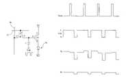
- FIG. 5The relationship between scan line and time in driving structure of the image frame is shown in FIG. 5 .
- the U.S. Pat. No. 6,677,713uses an amorphous silicon secondary transistor 25 to recover the threshold voltage Vth of driving transistor 22 to its initial value, and prevents Vth from increasing beyond its original value, and from the degradation of driving transistor 22 with time, so the problem of difference in brightness of each sub-pixel on the display panel can be resolved.
- an amorphous silicon transistor and a secondary scan line 28have to be added to each sub-pixel to process settings of the negative driving bias.
- a set of scan driverneed to be added to the system which will increase the complexity in manufacturing and, with the additional driving circuitry, substantially increase its cost.
- this inventionproposes an innovated way to improve the stability of a driving device for organic electric-excited light emitting transistor driven by amorphous silicon thin film transistor, the main purpose is to eliminate the non-uniformity of the threshold voltage Vth on thin film transistor, and extend life of the active matrix display panels.
- Another purposeis to achieve the same result as in U.S. Pat. No. 6,677,713 without additional transistors or scan lines. That is, this invention involves a simpler system, which implies a lower cost for the manufacturers employing it.
- this inventionpropose a driving scheme, the circuitry of which involves a driving transistor with its drain connected to power supply Vdd, its source connected to the anode of a light emitting diode. The cathode of light emitting diode is then connected to a comparatively fixed low potential Vss.
- a scan transistorwith its gate connected to the scan line, its source connected to data line and the drain connected to the gate of a driving transistor and an end of a storage capacitance. The other end of the storage capacitance is connected to a resetting signal line, which provides a resetting signal Vcom of high potential V 1 and low potential V 2 time pulses.
- a low potential V 2 input to the storage capacitancetoggles the gate of transistor to negative potential and temporarily prevent the organic light emitting diode (OLED) from emitting light
- a high potential V 1 input to the storage capacitancetoggles the gate of transistor to positive potential and trigger the organic light emitting diode (OLED) to emit light. That is, the positive or negative bias driven by driving transistor in each sub-pixel on display panel can be controlled through a single resetting signal voltage Vcom.
- FIG. 1is a schematic diagram of driving circuitry in a sub-pixel on conventional display device.
- FIG. 2is a schematic diagram of the relationship between scan lines and time for the driving structure of each frame of image on conventional display devices.
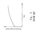
- FIG. 3is a diagram showing the variation of threshold voltage with operation time for driving transistors on traditional display devices.
- FIG. 4is a schematic diagram of the driving circuitry in each sub-pixel on U.S. Pat. No. 6,677,713.
- FIG. 5is a schematic diagram showing the relationship between scan lines and time for the driving structure.
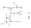
- FIG. 6is a schematic diagram of driving circuitry in a sub-pixel on this invention.
- FIG. 7is a schematic diagram of the connection and control of each sub-pixel on display panel of this invention.
- FIG. 8is a schematic diagram of the driving structure for this invention.
- FIG. 9is a schematic diagram of the time sequence of control signal corresponding to FIG. 8 .
- FIG. 10is a diagram showing the variation of the control signals, Vg, in FIG. 8 and FIG. 9 with Vs.
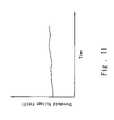
- FIG. 11is a diagram showing the variation of the threshold voltage Vth of the driving transistor with time.
- each data line 36 and each scan line 37 on the display deviceform a matrix of m ⁇ n sub-pixels on the display panel.
- the driving circuitry for each sub-pixelincludes two TFT and a capacitance.
- the organic light emitting diode (OLED) 34is driven by a driving transistor T 2 , the drain (D) of which is connected to the power source Vdd, and the source (S) to the anode of the organic light emitting diode 34 .
- the cathode of the organic light emitting diode 34is connected to a comparatively fixed low potential Vss (for example to the ground as zero potential).
- Vssfor example to the ground as zero potential.
- the gate (G) of a scanning transistoris connected to scan line 37
- the source (S)is connected to data line 36
- the drain (D)to the gate (G) of driving transistor T 2 and one end of storage capacitance.
- the other end of the storage capacitance C in each sub-pixel on the panelis connected to a resetting signal line 38 , which provides a resetting signal Vcom, synchronized with the resetting signal Vcom in every other sub-pixel on the panel.
- the driving structure of this invention and the corresponding time sequence of control signalare shown in FIGS. 8 and 9 where the scan operation begins with the first line of the Nth-frame, and proceeds consecutively to the last line of the frame.
- the resetting signalis maintained at high potential V 1 .
- the resetting signalis lowered to potential V 2 , and maintains on that level during closure time T OFF .
- the resetting signalis then increased to high potential level V 1 , before starting to scan the first line of the (n+1)th-frame.
- the remaining framesare operated with the same driving principle.
- the scanning signal Vscan on scan line 37will trigger scanning transistor T 1 , and send the data signal Vdata representing gray scale data on data line 36 , into an end of storage capacitance C.
- Thiscan be used to control the gate (G) of driving transistor T 2 , which incurs different Vgs voltages at different gate voltages Vg, and produces different driving current.
- Vgs potential on driving transistor T 2is positive (Vg is greater than Vs), which implies all transistors T 2 in sub-pixels on the display panel are at positive stress (Ps).
- the gate voltage Vg on transistor T 2When the resetting signal Vcom at high potential V 1 is decreased to the low potential V 2 , the gate voltage Vg on transistor T 2 will drop from Vdata to [Vdata ⁇ (V 1 ⁇ V 2 )], decreased by a level of (V 1 ⁇ V 2 ), since the storage capacitance maintains the potential difference across both ends.
- V 1 and V 2 voltagesfor example a V 1 of 20 volts and a V 2 of ⁇ 10 volts
- the gate voltage Vg on transistor T 2becomes negative, therefore no current is output to the organic light emitting diode 34 , and the source voltage Vs of driving transistor T 2 will be at closure voltage, Voled/off, of the organic light emitting diode 34 (if Vss is zero).
- Vgs value on transistor T 2will be a negative value [Vdata ⁇ (V 1 ⁇ V 2 ) ⁇ Voled/off] (Vg is lower than Vs, as shown in FIG. 10 ), which implies all transistors T 2 in the sub-pixels on the display panel are at negative stress (Ns).
- the Vgs voltage in driving transistor T 2is under alternating positive and negative stresses which lowers the degradation rate of a-Si TFT devices, inhibits positive shift as a result of critical potential Vth on driving transistor, and increases the stability of a-Si TFT device as shown in FIG. 11 .
- the improvement of driving structure to enhance the stability of organic electric-excited light emitting display device driven by amorphous silicon thin film transistorhas the following advantages:
Landscapes
- Engineering & Computer Science (AREA)
- Physics & Mathematics (AREA)
- Computer Hardware Design (AREA)
- General Physics & Mathematics (AREA)
- Theoretical Computer Science (AREA)
- Control Of Indicators Other Than Cathode Ray Tubes (AREA)
- Control Of El Displays (AREA)
Abstract
Description
The present invention is about driving an amorphous silicon thin-film transistor, more particularly driving an organic light emitting diode (OLED) display, to enhance the stability of the threshold voltage (Vth) as a function of time on the amorphous silicon thin-film transistors.
There are two ways to drive an organic light emitting display (OLED): one is passive matrix driving and the other is active matrix driving. In an active matrix device, a good service life and high resolution can be achieved without being driven to an extremely high brightness. Therefore, OLED combined with thin-film transistor (TFT) to realize the active matrix technology conforms to the present market requirements for fluidity of images as well as higher and higher resolution in display panels that fully demonstrate the superior properties of OLED. As a result of the continuous improvements in light emitting efficiency on OLED materials, using amorphous silicon thin-film transistor (a-Si TFT) as the driving platform for OLED devices is no longer infeasible. As a result of the maturity of manufacturing processes and equipments in a-Si TFT, a lower manufacturing cost can be achieved which greatly lower the over-all cost of the active matrix OLED.
Although a-Si TFT has absolute advantage of lower cost, there are still technical issues needed to improve if a-Si TFT is to be used to drive OLED. Two major goals must be achieved. The first goal is to improve the stability of the a-Si TFT device, and the second is to increase the driving capability of current in the a-Si TFT device.
The fundamental working principle is as follows: Through controlling the signal ofscan line 17 to triggertransistor 11 ON, which then input the voltage signal representing gray scale data of image intostorage capacitance 13 to control the gate oftransistor 12. The current is flowing through thetransistor 12, which can be varied by changing the gate voltage Vgs, oftransistor 12. Naturally, in order to maketransistor 12 produce a driving current, the Vgs value intransistor 12 must be greater than its threshold voltage Vth.
Conventional scanning structure employs a continuous scanning mode, beginning with the first line on the (n)th-frame, and consecutively scan to the last line of the frame, immediately followed by the first line on the (n+1)th-frame, and consecutively scan to the last line of the (n+1)th frame, as shown inFIG. 2 .
The conventional scan mode stated above, when applied to OLED structures driven by a-Si TFT, will produce a continuous positive Vgs voltage ontransistor 12. A continuous positive Vgs bias, called Positive Stress, it will rapidly degrade the a-Si TFT devices ontransistor 12. Also, the threshold voltage, Vth, ontransistor 12 will increase with time instead of maintaining at the original level which will incur a “Positive Shift” as shown inFIG. 3 . Therefore long term stability of a-Si TFT driving devices ontransistor 12 can not be achieved if conventional a-Si TFT driving circuitry is employed.
Therefore, the positive shift as a result of instability in threshold voltage, Vth, brings about two problems: The first is that the original brightness of OLED can not be maintained as a result of the decrease in output current ontransistor 12, with time. The second problem is that the degree of degradation ontransistor 12 in the sub-pixel varies with time. Because the difference in positive stress ontransistor 12 of each sub-pixel will bring about a difference in brightness on the sub-pixel of the display panel, resulting in so called “Temporal Non-Uniformity”.
To solve the weaknesses mentioned above, the U.S. Pat. No. 6,677,713 “Driving Circuit and Method for Light Emitting Device” proposed 3T1C driving circuitry as shown inFIG. 4 . The driving circuitry of the pixel includes adriving transistor 22 with the gate (G) connected to node B, alight emitting device 24 connected in serial to the driving transistor forming a light emitting path. The light emitting path is then attached between the system high voltage, Vdd, and system low voltage, Vss. When drivingtransistor 22 is turned on, the system high voltage, Vdd, triggers thelight emitting device 24 and emits light. Acapacitance 23 connected to node B, is used to maintain the On or Off position ofdriving transistor 22. Also, a driving circuit consists of aprimary transistor 21 and asecondary transistor 25 is connected in parallel to node B. The gate (G) ofprimary transistor 21 receives a time pulse, S1, ofprimary scan line 27, and gate (G) ofsecondary transistor 25 receives a time pulse, S2, ofsecondary scan line 28. The primary scan pulse S1 and the secondary scanning pulse S2 have the same frequency, but there is a time delay in the secondary scan pulse S2 compared with the primary scan pulse S1.
Therefore the working principle is that when even number of continuous primary scanning pulseS1 trigger transistor 21 On, allows the data voltage indata line 26 corresponding to a frame of image to input to node B, toggles thedriving transistor 22 On, And proceeds a time-interval, TON, of image display; when even number of continuous secondary scanning pulseS2 triggers transistor 25 On, allows a closure voltage Vref2 into node. B, andtoggles transistor 22 Off, and proceeds a time-interval TOFFof image off. The relationship between scan line and time in driving structure of the image frame is shown inFIG. 5 .
The U.S. Pat. No. 6,677,713, as compared to the conventional technology, uses an amorphous siliconsecondary transistor 25 to recover the threshold voltage Vth ofdriving transistor 22 to its initial value, and prevents Vth from increasing beyond its original value, and from the degradation of drivingtransistor 22 with time, so the problem of difference in brightness of each sub-pixel on the display panel can be resolved.
However in the patent, an amorphous silicon transistor and asecondary scan line 28 have to be added to each sub-pixel to process settings of the negative driving bias. In other words, a set of scan driver need to be added to the system which will increase the complexity in manufacturing and, with the additional driving circuitry, substantially increase its cost.
Therefore this invention proposes an innovated way to improve the stability of a driving device for organic electric-excited light emitting transistor driven by amorphous silicon thin film transistor, the main purpose is to eliminate the non-uniformity of the threshold voltage Vth on thin film transistor, and extend life of the active matrix display panels.
Another purpose is to achieve the same result as in U.S. Pat. No. 6,677,713 without additional transistors or scan lines. That is, this invention involves a simpler system, which implies a lower cost for the manufacturers employing it.
To achieve the objectives mentioned above, this invention propose a driving scheme, the circuitry of which involves a driving transistor with its drain connected to power supply Vdd, its source connected to the anode of a light emitting diode. The cathode of light emitting diode is then connected to a comparatively fixed low potential Vss. A scan transistor, with its gate connected to the scan line, its source connected to data line and the drain connected to the gate of a driving transistor and an end of a storage capacitance. The other end of the storage capacitance is connected to a resetting signal line, which provides a resetting signal Vcom of high potential V1 and low potential V2 time pulses.
According to the resetting signal Vcom time pulse a low potential V2 input to the storage capacitance toggles the gate of transistor to negative potential and temporarily prevent the organic light emitting diode (OLED) from emitting light, whereas a high potential V1 input to the storage capacitance toggles the gate of transistor to positive potential and trigger the organic light emitting diode (OLED) to emit light. That is, the positive or negative bias driven by driving transistor in each sub-pixel on display panel can be controlled through a single resetting signal voltage Vcom.
Further scope of the applicability of the present invention will become apparent from the detailed description given hereinafter. However, it should be understood that the detailed description and specific examples, while indicating preferred embodiments of the invention, are given by way of illustration only, since various changes and modifications within the spirit and scope of the invention will become apparent to those skilled in the art from this detailed description.
The present invention will become more fully understood from the detailed description given hereinbelow and the accompanying drawings which are given by way of illustration only, and thus are not limitative of the present invention, and wherein:
The driving circuitry for each sub-pixel in this invention and the schematic diagram of the connection as well as control of each sub-pixel on display panel are shown inFIGS. 6 and 7 . As shown in the figures, eachdata line 36 and eachscan line 37 on the display device form a matrix of m×n sub-pixels on the display panel. The driving circuitry for each sub-pixel includes two TFT and a capacitance. The organic light emitting diode (OLED)34 is driven by a driving transistor T2, the drain (D) of which is connected to the power source Vdd, and the source (S) to the anode of the organiclight emitting diode 34. The cathode of the organiclight emitting diode 34 is connected to a comparatively fixed low potential Vss (for example to the ground as zero potential). Besides, the gate (G) of a scanning transistor is connected to scanline 37, the source (S) is connected todata line 36, and the drain (D) to the gate (G) of driving transistor T2 and one end of storage capacitance. In contrast to the conventional design, the other end of the storage capacitance C in each sub-pixel on the panel is connected to aresetting signal line 38, which provides a resetting signal Vcom, synchronized with the resetting signal Vcom in every other sub-pixel on the panel.
The driving structure of this invention and the corresponding time sequence of control signal are shown inFIGS. 8 and 9 where the scan operation begins with the first line of the Nth-frame, and proceeds consecutively to the last line of the frame. During this period of display time TON, the resetting signal is maintained at high potential V1. After finish scanning the last line of the frame, the resetting signal is lowered to potential V2, and maintains on that level during closure time TOFF. The resetting signal is then increased to high potential level V1, before starting to scan the first line of the (n+1)th-frame. The remaining frames are operated with the same driving principle.
When the resetting signal Vcom is at high potential level V1, the scanning signal Vscan onscan line 37 will trigger scanning transistor T1, and send the data signal Vdata representing gray scale data ondata line 36, into an end of storage capacitance C. This can be used to control the gate (G) of driving transistor T2, which incurs different Vgs voltages at different gate voltages Vg, and produces different driving current. Now the Vgs potential on driving transistor T2 is positive (Vg is greater than Vs), which implies all transistors T2 in sub-pixels on the display panel are at positive stress (Ps).
When the resetting signal Vcom at high potential V1 is decreased to the low potential V2, the gate voltage Vg on transistor T2 will drop from Vdata to [Vdata−(V1−V2)], decreased by a level of (V1−V2), since the storage capacitance maintains the potential difference across both ends. Through proper choice of V1 and V2 voltages (for example a V1 of 20 volts and a V2 of −10 volts), the gate voltage Vg on transistor T2 becomes negative, therefore no current is output to the organiclight emitting diode 34, and the source voltage Vs of driving transistor T2 will be at closure voltage, Voled/off, of the organic light emitting diode34 (if Vss is zero). At the same time, Vgs value on transistor T2 will be a negative value [Vdata−(V1−V2)−Voled/off] (Vg is lower than Vs, as shown inFIG. 10 ), which implies all transistors T2 in the sub-pixels on the display panel are at negative stress (Ns).
As compared with the traditional driving scheme in which Vgs voltage in drivingtransistor 12 is constantly maintained at positive stress and produce a phenomenon called “positive shift”. In this invention, the Vgs voltage in driving transistor T2 is under alternating positive and negative stresses which lowers the degradation rate of a-Si TFT devices, inhibits positive shift as a result of critical potential Vth on driving transistor, and increases the stability of a-Si TFT device as shown inFIG. 11 .
In summary, the improvement of driving structure to enhance the stability of organic electric-excited light emitting display device driven by amorphous silicon thin film transistor has the following advantages:
- 1. Through alternating positive and negative stresses, a lower degradation rate of a-Si TFT device, and higher stability of organic electric-excited light emitting display device driven by amorphous silicon thin film transistor can be achieved.
- 2. Improving the stability of organic electric-excited light emitting display device driven by amorphous silicon thin film transistor will extend the life of active matrix display panel.
- 3. Without any increase in the number of transistors or scan lines, this invention is as simple to manufacture as the conventional scheme, whereas offers the same effect as in the U.S. Pat. No. 6,677,713.
Therefore the difference in driving structure between present invention and the U.S. Pat. No. 6,677,713 is that in this proposed technology, after the data of each scan line in the (n)th image frame on the panel is written, each scan line holds a different period of time before entering negative stress, hence the driving transistors of each sub-pixel on the display device are negative stressed at the same time. However in the U.S. Pat. No. 6,677,713, after the data of each scan line in the Nth image frame on the panel is written, each scan line holds the same period of time before entering negative stress, hence the driving transistors of each sub-pixel on the display device are negatively stressed consecutively rather than simultaneously.
Although there is a difference in driving structure, both technologies provide the same effect to the vision, and both utilize the phenomenon of persistence of vision. The eye will not perceive the flickering of an image with frequency higher than 60 Hz. This invention shares the same objectives and effects the U.S. Pat. No. 6,677,713 provides, but with a decreased complexity of system and lower cost for driving circuitry.
The invention being thus described, it will be obvious that the same may be varied in many ways. Such variations are not to be regarded as a departure from the spirit and scope of the invention, and all such modifications as would be obvious to one skilled in the art are intended to be included within the scope of the following claims.
Claims (3)
1. A method of improving the stability of an organic light emitting display device driven by an amorphous silicon thin film transistor, driving circuitry for driving the organic light-emitting display device including a driving transistor with a drain connected to a first power source, a source connected to an anode of an organic light emitting diode, a scan transistor having a gate connected to a scan line, a source connected to a data line and a drain connected to the gate of the driving transistor and one end of a storage capacitance, another end of the storage capacitance being connected to a resetting signal line, the method comprising the steps of:
driving each sub-pixel in active matrix organic light emitting diode display devices;
providing said driving circuitry for said driving;
connecting a cathode of the organic light emitting diode to a comparatively fixed low potential;
providing said scan transistor having a gate connected to scan line;
connecting the other end of the storage capacitance to a resetting signal line, to provide a time pulse for resetting signal Vcom of high potential V1 and low potential V2;
toggling the gate of the driving transistor to a negative voltage by the lower output voltage V2 at the storage capacitance in accordance with the time pulse of the applied resetting signal Vcom, which temporarily prevents the organic light emitting diode from emitting light.
2. The method according toclaim 1 , wherein the high potential V1 at the storage capacitance from the time pulse of resetting signal Vcom toggles the gate of the driving transistor to a positive voltage, which renders the organic light emitting diode to emit light.
3. The method according toclaim 1 , wherein the resetting signal Vcom is synchronized for each sub-pixel on the display device.
Priority Applications (1)
| Application Number | Priority Date | Filing Date | Title |
|---|---|---|---|
| US10/998,550US7116058B2 (en) | 2004-11-30 | 2004-11-30 | Method of improving the stability of active matrix OLED displays driven by amorphous silicon thin-film transistors |
Applications Claiming Priority (1)
| Application Number | Priority Date | Filing Date | Title |
|---|---|---|---|
| US10/998,550US7116058B2 (en) | 2004-11-30 | 2004-11-30 | Method of improving the stability of active matrix OLED displays driven by amorphous silicon thin-film transistors |
Publications (2)
| Publication Number | Publication Date |
|---|---|
| US20060113918A1 US20060113918A1 (en) | 2006-06-01 |
| US7116058B2true US7116058B2 (en) | 2006-10-03 |
Family
ID=36566743
Family Applications (1)
| Application Number | Title | Priority Date | Filing Date |
|---|---|---|---|
| US10/998,550Expired - Fee RelatedUS7116058B2 (en) | 2004-11-30 | 2004-11-30 | Method of improving the stability of active matrix OLED displays driven by amorphous silicon thin-film transistors |
Country Status (1)
| Country | Link |
|---|---|
| US (1) | US7116058B2 (en) |
Cited By (87)
| Publication number | Priority date | Publication date | Assignee | Title |
|---|---|---|---|---|
| US20060284801A1 (en)* | 2005-06-20 | 2006-12-21 | Lg Philips Lcd Co., Ltd. | Driving circuit for organic light emitting diode, display device using the same and driving method of organic light emitting diode display device |
| WO2007118332A1 (en)* | 2006-04-19 | 2007-10-25 | Ignis Innovation Inc. | Stable driving scheme for active matrix displays |
| US20080191976A1 (en)* | 2004-06-29 | 2008-08-14 | Arokia Nathan | Voltage-Programming Scheme for Current-Driven Arnoled Displays |
| US20090160740A1 (en)* | 2007-12-21 | 2009-06-25 | Leon Felipe A | Electroluminescent display compensated analog transistor drive signal |
| US20090221209A1 (en)* | 2008-03-03 | 2009-09-03 | Jae-Kook Ha | Method of manufacturing a light-emitting element and method of manufacturing a display substrate using the same |
| US20090262101A1 (en)* | 2008-04-16 | 2009-10-22 | Ignis Innovation Inc. | Pixel circuit, display system and driving method thereof |
| US20090284453A1 (en)* | 2008-05-13 | 2009-11-19 | Kyoung-Ju Shin | Display device and method of driving the same |
| US20100225634A1 (en)* | 2009-03-04 | 2010-09-09 | Levey Charles I | Electroluminescent display compensated drive signal |
| US20100225630A1 (en)* | 2009-03-03 | 2010-09-09 | Levey Charles I | Electroluminescent subpixel compensated drive signal |
| US8599191B2 (en) | 2011-05-20 | 2013-12-03 | Ignis Innovation Inc. | System and methods for extraction of threshold and mobility parameters in AMOLED displays |
| US8659518B2 (en) | 2005-01-28 | 2014-02-25 | Ignis Innovation Inc. | Voltage programmed pixel circuit, display system and driving method thereof |
| US8664644B2 (en) | 2001-02-16 | 2014-03-04 | Ignis Innovation Inc. | Pixel driver circuit and pixel circuit having the pixel driver circuit |
| US8803417B2 (en) | 2009-12-01 | 2014-08-12 | Ignis Innovation Inc. | High resolution pixel architecture |
| US8816946B2 (en) | 2004-12-15 | 2014-08-26 | Ignis Innovation Inc. | Method and system for programming, calibrating and driving a light emitting device display |
| US8901579B2 (en) | 2011-08-03 | 2014-12-02 | Ignis Innovation Inc. | Organic light emitting diode and method of manufacturing |
| US8907991B2 (en) | 2010-12-02 | 2014-12-09 | Ignis Innovation Inc. | System and methods for thermal compensation in AMOLED displays |
| US8922544B2 (en) | 2012-05-23 | 2014-12-30 | Ignis Innovation Inc. | Display systems with compensation for line propagation delay |
| US8941697B2 (en) | 2003-09-23 | 2015-01-27 | Ignis Innovation Inc. | Circuit and method for driving an array of light emitting pixels |
| US8994617B2 (en) | 2010-03-17 | 2015-03-31 | Ignis Innovation Inc. | Lifetime uniformity parameter extraction methods |
| US9070775B2 (en) | 2011-08-03 | 2015-06-30 | Ignis Innovations Inc. | Thin film transistor |
| US9093028B2 (en) | 2009-12-06 | 2015-07-28 | Ignis Innovation Inc. | System and methods for power conservation for AMOLED pixel drivers |
| US9093029B2 (en) | 2011-05-20 | 2015-07-28 | Ignis Innovation Inc. | System and methods for extraction of threshold and mobility parameters in AMOLED displays |
| US9111485B2 (en) | 2009-06-16 | 2015-08-18 | Ignis Innovation Inc. | Compensation technique for color shift in displays |
| US9125278B2 (en) | 2006-08-15 | 2015-09-01 | Ignis Innovation Inc. | OLED luminance degradation compensation |
| US9134825B2 (en) | 2011-05-17 | 2015-09-15 | Ignis Innovation Inc. | Systems and methods for display systems with dynamic power control |
| US9153172B2 (en) | 2004-12-07 | 2015-10-06 | Ignis Innovation Inc. | Method and system for programming and driving active matrix light emitting device pixel having a controllable supply voltage |
| US9171500B2 (en) | 2011-05-20 | 2015-10-27 | Ignis Innovation Inc. | System and methods for extraction of parasitic parameters in AMOLED displays |
| US9171504B2 (en) | 2013-01-14 | 2015-10-27 | Ignis Innovation Inc. | Driving scheme for emissive displays providing compensation for driving transistor variations |
| US9275579B2 (en) | 2004-12-15 | 2016-03-01 | Ignis Innovation Inc. | System and methods for extraction of threshold and mobility parameters in AMOLED displays |
| US9280933B2 (en) | 2004-12-15 | 2016-03-08 | Ignis Innovation Inc. | System and methods for extraction of threshold and mobility parameters in AMOLED displays |
| US9305488B2 (en) | 2013-03-14 | 2016-04-05 | Ignis Innovation Inc. | Re-interpolation with edge detection for extracting an aging pattern for AMOLED displays |
| US9311859B2 (en) | 2009-11-30 | 2016-04-12 | Ignis Innovation Inc. | Resetting cycle for aging compensation in AMOLED displays |
| US9324268B2 (en) | 2013-03-15 | 2016-04-26 | Ignis Innovation Inc. | Amoled displays with multiple readout circuits |
| US9336717B2 (en) | 2012-12-11 | 2016-05-10 | Ignis Innovation Inc. | Pixel circuits for AMOLED displays |
| US9343006B2 (en) | 2012-02-03 | 2016-05-17 | Ignis Innovation Inc. | Driving system for active-matrix displays |
| US9384698B2 (en) | 2009-11-30 | 2016-07-05 | Ignis Innovation Inc. | System and methods for aging compensation in AMOLED displays |
| US9385169B2 (en) | 2011-11-29 | 2016-07-05 | Ignis Innovation Inc. | Multi-functional active matrix organic light-emitting diode display |
| US9430958B2 (en) | 2010-02-04 | 2016-08-30 | Ignis Innovation Inc. | System and methods for extracting correlation curves for an organic light emitting device |
| US9437137B2 (en) | 2013-08-12 | 2016-09-06 | Ignis Innovation Inc. | Compensation accuracy |
| US9466240B2 (en) | 2011-05-26 | 2016-10-11 | Ignis Innovation Inc. | Adaptive feedback system for compensating for aging pixel areas with enhanced estimation speed |
| US9502653B2 (en) | 2013-12-25 | 2016-11-22 | Ignis Innovation Inc. | Electrode contacts |
| US9530349B2 (en) | 2011-05-20 | 2016-12-27 | Ignis Innovations Inc. | Charged-based compensation and parameter extraction in AMOLED displays |
| US9606607B2 (en) | 2011-05-17 | 2017-03-28 | Ignis Innovation Inc. | Systems and methods for display systems with dynamic power control |
| US9741282B2 (en) | 2013-12-06 | 2017-08-22 | Ignis Innovation Inc. | OLED display system and method |
| US9747834B2 (en) | 2012-05-11 | 2017-08-29 | Ignis Innovation Inc. | Pixel circuits including feedback capacitors and reset capacitors, and display systems therefore |
| US9761170B2 (en) | 2013-12-06 | 2017-09-12 | Ignis Innovation Inc. | Correction for localized phenomena in an image array |
| US9773439B2 (en) | 2011-05-27 | 2017-09-26 | Ignis Innovation Inc. | Systems and methods for aging compensation in AMOLED displays |
| US9786223B2 (en) | 2012-12-11 | 2017-10-10 | Ignis Innovation Inc. | Pixel circuits for AMOLED displays |
| US9786209B2 (en) | 2009-11-30 | 2017-10-10 | Ignis Innovation Inc. | System and methods for aging compensation in AMOLED displays |
| US9799246B2 (en) | 2011-05-20 | 2017-10-24 | Ignis Innovation Inc. | System and methods for extraction of threshold and mobility parameters in AMOLED displays |
| US9818376B2 (en) | 2009-11-12 | 2017-11-14 | Ignis Innovation Inc. | Stable fast programming scheme for displays |
| US9830857B2 (en) | 2013-01-14 | 2017-11-28 | Ignis Innovation Inc. | Cleaning common unwanted signals from pixel measurements in emissive displays |
| US9842889B2 (en) | 2014-11-28 | 2017-12-12 | Ignis Innovation Inc. | High pixel density array architecture |
| US9851854B2 (en) | 2014-12-16 | 2017-12-26 | Microsoft Technology Licensing, Llc | Touch display device |
| US9881532B2 (en) | 2010-02-04 | 2018-01-30 | Ignis Innovation Inc. | System and method for extracting correlation curves for an organic light emitting device |
| US9934725B2 (en) | 2013-03-08 | 2018-04-03 | Ignis Innovation Inc. | Pixel circuits for AMOLED displays |
| US9947293B2 (en) | 2015-05-27 | 2018-04-17 | Ignis Innovation Inc. | Systems and methods of reduced memory bandwidth compensation |
| US9952698B2 (en) | 2013-03-15 | 2018-04-24 | Ignis Innovation Inc. | Dynamic adjustment of touch resolutions on an AMOLED display |
| US10012678B2 (en) | 2004-12-15 | 2018-07-03 | Ignis Innovation Inc. | Method and system for programming, calibrating and/or compensating, and driving an LED display |
| US10013907B2 (en) | 2004-12-15 | 2018-07-03 | Ignis Innovation Inc. | Method and system for programming, calibrating and/or compensating, and driving an LED display |
| US10019941B2 (en) | 2005-09-13 | 2018-07-10 | Ignis Innovation Inc. | Compensation technique for luminance degradation in electro-luminance devices |
| US10074304B2 (en) | 2015-08-07 | 2018-09-11 | Ignis Innovation Inc. | Systems and methods of pixel calibration based on improved reference values |
| US10078984B2 (en) | 2005-02-10 | 2018-09-18 | Ignis Innovation Inc. | Driving circuit for current programmed organic light-emitting diode displays |
| US10089924B2 (en) | 2011-11-29 | 2018-10-02 | Ignis Innovation Inc. | Structural and low-frequency non-uniformity compensation |
| US10089921B2 (en) | 2010-02-04 | 2018-10-02 | Ignis Innovation Inc. | System and methods for extracting correlation curves for an organic light emitting device |
| US10163996B2 (en) | 2003-02-24 | 2018-12-25 | Ignis Innovation Inc. | Pixel having an organic light emitting diode and method of fabricating the pixel |
| US10163401B2 (en) | 2010-02-04 | 2018-12-25 | Ignis Innovation Inc. | System and methods for extracting correlation curves for an organic light emitting device |
| US10176752B2 (en) | 2014-03-24 | 2019-01-08 | Ignis Innovation Inc. | Integrated gate driver |
| US10176736B2 (en) | 2010-02-04 | 2019-01-08 | Ignis Innovation Inc. | System and methods for extracting correlation curves for an organic light emitting device |
| US10181282B2 (en) | 2015-01-23 | 2019-01-15 | Ignis Innovation Inc. | Compensation for color variations in emissive devices |
| US10192479B2 (en) | 2014-04-08 | 2019-01-29 | Ignis Innovation Inc. | Display system using system level resources to calculate compensation parameters for a display module in a portable device |
| US10204540B2 (en) | 2015-10-26 | 2019-02-12 | Ignis Innovation Inc. | High density pixel pattern |
| US10235933B2 (en) | 2005-04-12 | 2019-03-19 | Ignis Innovation Inc. | System and method for compensation of non-uniformities in light emitting device displays |
| US10311780B2 (en) | 2015-05-04 | 2019-06-04 | Ignis Innovation Inc. | Systems and methods of optical feedback |
| US10319307B2 (en) | 2009-06-16 | 2019-06-11 | Ignis Innovation Inc. | Display system with compensation techniques and/or shared level resources |
| US10373554B2 (en) | 2015-07-24 | 2019-08-06 | Ignis Innovation Inc. | Pixels and reference circuits and timing techniques |
| US10388221B2 (en) | 2005-06-08 | 2019-08-20 | Ignis Innovation Inc. | Method and system for driving a light emitting device display |
| US10410579B2 (en) | 2015-07-24 | 2019-09-10 | Ignis Innovation Inc. | Systems and methods of hybrid calibration of bias current |
| US10573231B2 (en) | 2010-02-04 | 2020-02-25 | Ignis Innovation Inc. | System and methods for extracting correlation curves for an organic light emitting device |
| US10586491B2 (en) | 2016-12-06 | 2020-03-10 | Ignis Innovation Inc. | Pixel circuits for mitigation of hysteresis |
| US10657895B2 (en) | 2015-07-24 | 2020-05-19 | Ignis Innovation Inc. | Pixels and reference circuits and timing techniques |
| US10714018B2 (en) | 2017-05-17 | 2020-07-14 | Ignis Innovation Inc. | System and method for loading image correction data for displays |
| US10867536B2 (en) | 2013-04-22 | 2020-12-15 | Ignis Innovation Inc. | Inspection system for OLED display panels |
| US10971078B2 (en) | 2018-02-12 | 2021-04-06 | Ignis Innovation Inc. | Pixel measurement through data line |
| US10996258B2 (en) | 2009-11-30 | 2021-05-04 | Ignis Innovation Inc. | Defect detection and correction of pixel circuits for AMOLED displays |
| US10997901B2 (en) | 2014-02-28 | 2021-05-04 | Ignis Innovation Inc. | Display system |
| US11025899B2 (en) | 2017-08-11 | 2021-06-01 | Ignis Innovation Inc. | Optical correction systems and methods for correcting non-uniformity of emissive display devices |
Families Citing this family (9)
| Publication number | Priority date | Publication date | Assignee | Title |
|---|---|---|---|---|
| US7317434B2 (en)* | 2004-12-03 | 2008-01-08 | Dupont Displays, Inc. | Circuits including switches for electronic devices and methods of using the electronic devices |
| US8004479B2 (en)* | 2007-11-28 | 2011-08-23 | Global Oled Technology Llc | Electroluminescent display with interleaved 3T1C compensation |
| US8248341B2 (en)* | 2009-04-15 | 2012-08-21 | Store Electronic Systems Sa | Low power active matrix display |
| KR101658037B1 (en) | 2010-11-09 | 2016-09-21 | 삼성전자주식회사 | Method of driving active display device |
| KR101560239B1 (en)* | 2010-11-18 | 2015-10-26 | 엘지디스플레이 주식회사 | Organic light emitting diode display device and method for driving the same |
| TWI489191B (en)* | 2012-09-20 | 2015-06-21 | Au Optronics Corp | Pixel structure and thin film transistor |
| JP2015014764A (en)* | 2013-07-08 | 2015-01-22 | ソニー株式会社 | Display device, drive method of display device and electronic apparatus |
| CN108510946B (en)* | 2018-04-19 | 2019-12-31 | 京东方科技集团股份有限公司 | Pixel circuit, display panel and display device |
| CN113257196A (en) | 2021-05-14 | 2021-08-13 | Tcl华星光电技术有限公司 | Backlight driving circuit, control method thereof, display panel and electronic device |
Citations (5)
| Publication number | Priority date | Publication date | Assignee | Title |
|---|---|---|---|---|
| US6229508B1 (en)* | 1997-09-29 | 2001-05-08 | Sarnoff Corporation | Active matrix light emitting diode pixel structure and concomitant method |
| US6501466B1 (en)* | 1999-11-18 | 2002-12-31 | Sony Corporation | Active matrix type display apparatus and drive circuit thereof |
| US6677713B1 (en) | 2002-08-28 | 2004-01-13 | Au Optronics Corporation | Driving circuit and method for light emitting device |
| US6909242B2 (en)* | 2001-09-21 | 2005-06-21 | Semiconductor Energy Laboratory Co., Ltd. | Semiconductor device |
| US6950081B2 (en)* | 2001-10-10 | 2005-09-27 | Hitachi, Ltd. | Image display device |
- 2004
- 2004-11-30USUS10/998,550patent/US7116058B2/ennot_activeExpired - Fee Related
Patent Citations (5)
| Publication number | Priority date | Publication date | Assignee | Title |
|---|---|---|---|---|
| US6229508B1 (en)* | 1997-09-29 | 2001-05-08 | Sarnoff Corporation | Active matrix light emitting diode pixel structure and concomitant method |
| US6501466B1 (en)* | 1999-11-18 | 2002-12-31 | Sony Corporation | Active matrix type display apparatus and drive circuit thereof |
| US6909242B2 (en)* | 2001-09-21 | 2005-06-21 | Semiconductor Energy Laboratory Co., Ltd. | Semiconductor device |
| US6950081B2 (en)* | 2001-10-10 | 2005-09-27 | Hitachi, Ltd. | Image display device |
| US6677713B1 (en) | 2002-08-28 | 2004-01-13 | Au Optronics Corporation | Driving circuit and method for light emitting device |
Cited By (186)
| Publication number | Priority date | Publication date | Assignee | Title |
|---|---|---|---|---|
| US8890220B2 (en) | 2001-02-16 | 2014-11-18 | Ignis Innovation, Inc. | Pixel driver circuit and pixel circuit having control circuit coupled to supply voltage |
| US8664644B2 (en) | 2001-02-16 | 2014-03-04 | Ignis Innovation Inc. | Pixel driver circuit and pixel circuit having the pixel driver circuit |
| US10163996B2 (en) | 2003-02-24 | 2018-12-25 | Ignis Innovation Inc. | Pixel having an organic light emitting diode and method of fabricating the pixel |
| US8941697B2 (en) | 2003-09-23 | 2015-01-27 | Ignis Innovation Inc. | Circuit and method for driving an array of light emitting pixels |
| US9472139B2 (en) | 2003-09-23 | 2016-10-18 | Ignis Innovation Inc. | Circuit and method for driving an array of light emitting pixels |
| US9472138B2 (en) | 2003-09-23 | 2016-10-18 | Ignis Innovation Inc. | Pixel driver circuit with load-balance in current mirror circuit |
| US9852689B2 (en) | 2003-09-23 | 2017-12-26 | Ignis Innovation Inc. | Circuit and method for driving an array of light emitting pixels |
| US10089929B2 (en) | 2003-09-23 | 2018-10-02 | Ignis Innovation Inc. | Pixel driver circuit with load-balance in current mirror circuit |
| US20080191976A1 (en)* | 2004-06-29 | 2008-08-14 | Arokia Nathan | Voltage-Programming Scheme for Current-Driven Arnoled Displays |
| US8232939B2 (en) | 2004-06-29 | 2012-07-31 | Ignis Innovation, Inc. | Voltage-programming scheme for current-driven AMOLED displays |
| USRE45291E1 (en) | 2004-06-29 | 2014-12-16 | Ignis Innovation Inc. | Voltage-programming scheme for current-driven AMOLED displays |
| USRE47257E1 (en) | 2004-06-29 | 2019-02-26 | Ignis Innovation Inc. | Voltage-programming scheme for current-driven AMOLED displays |
| US8115707B2 (en) | 2004-06-29 | 2012-02-14 | Ignis Innovation Inc. | Voltage-programming scheme for current-driven AMOLED displays |
| US9153172B2 (en) | 2004-12-07 | 2015-10-06 | Ignis Innovation Inc. | Method and system for programming and driving active matrix light emitting device pixel having a controllable supply voltage |
| US9275579B2 (en) | 2004-12-15 | 2016-03-01 | Ignis Innovation Inc. | System and methods for extraction of threshold and mobility parameters in AMOLED displays |
| US10699624B2 (en) | 2004-12-15 | 2020-06-30 | Ignis Innovation Inc. | Method and system for programming, calibrating and/or compensating, and driving an LED display |
| US8816946B2 (en) | 2004-12-15 | 2014-08-26 | Ignis Innovation Inc. | Method and system for programming, calibrating and driving a light emitting device display |
| US9280933B2 (en) | 2004-12-15 | 2016-03-08 | Ignis Innovation Inc. | System and methods for extraction of threshold and mobility parameters in AMOLED displays |
| US9970964B2 (en) | 2004-12-15 | 2018-05-15 | Ignis Innovation Inc. | Method and system for programming, calibrating and driving a light emitting device display |
| US10012678B2 (en) | 2004-12-15 | 2018-07-03 | Ignis Innovation Inc. | Method and system for programming, calibrating and/or compensating, and driving an LED display |
| US8994625B2 (en) | 2004-12-15 | 2015-03-31 | Ignis Innovation Inc. | Method and system for programming, calibrating and driving a light emitting device display |
| US10013907B2 (en) | 2004-12-15 | 2018-07-03 | Ignis Innovation Inc. | Method and system for programming, calibrating and/or compensating, and driving an LED display |
| US8659518B2 (en) | 2005-01-28 | 2014-02-25 | Ignis Innovation Inc. | Voltage programmed pixel circuit, display system and driving method thereof |
| US9728135B2 (en) | 2005-01-28 | 2017-08-08 | Ignis Innovation Inc. | Voltage programmed pixel circuit, display system and driving method thereof |
| US9373645B2 (en) | 2005-01-28 | 2016-06-21 | Ignis Innovation Inc. | Voltage programmed pixel circuit, display system and driving method thereof |
| US10078984B2 (en) | 2005-02-10 | 2018-09-18 | Ignis Innovation Inc. | Driving circuit for current programmed organic light-emitting diode displays |
| US10235933B2 (en) | 2005-04-12 | 2019-03-19 | Ignis Innovation Inc. | System and method for compensation of non-uniformities in light emitting device displays |
| US10388221B2 (en) | 2005-06-08 | 2019-08-20 | Ignis Innovation Inc. | Method and system for driving a light emitting device display |
| US7675493B2 (en)* | 2005-06-20 | 2010-03-09 | Lg. Display Co., Ltd. | Driving circuit for organic light emitting diode, display device using the same and driving method of organic light emitting diode display device |
| US20060284801A1 (en)* | 2005-06-20 | 2006-12-21 | Lg Philips Lcd Co., Ltd. | Driving circuit for organic light emitting diode, display device using the same and driving method of organic light emitting diode display device |
| US10019941B2 (en) | 2005-09-13 | 2018-07-10 | Ignis Innovation Inc. | Compensation technique for luminance degradation in electro-luminance devices |
| US9633597B2 (en) | 2006-04-19 | 2017-04-25 | Ignis Innovation Inc. | Stable driving scheme for active matrix displays |
| US10453397B2 (en) | 2006-04-19 | 2019-10-22 | Ignis Innovation Inc. | Stable driving scheme for active matrix displays |
| US9842544B2 (en) | 2006-04-19 | 2017-12-12 | Ignis Innovation Inc. | Stable driving scheme for active matrix displays |
| US8477121B2 (en) | 2006-04-19 | 2013-07-02 | Ignis Innovation, Inc. | Stable driving scheme for active matrix displays |
| WO2007118332A1 (en)* | 2006-04-19 | 2007-10-25 | Ignis Innovation Inc. | Stable driving scheme for active matrix displays |
| US20070247398A1 (en)* | 2006-04-19 | 2007-10-25 | Ignis Innovation Inc. | Stable driving scheme for active matrix displays |
| US10127860B2 (en) | 2006-04-19 | 2018-11-13 | Ignis Innovation Inc. | Stable driving scheme for active matrix displays |
| US20200005715A1 (en)* | 2006-04-19 | 2020-01-02 | Ignis Innovation Inc. | Stable driving scheme for active matrix displays |
| US10650754B2 (en)* | 2006-04-19 | 2020-05-12 | Ignis Innovation Inc. | Stable driving scheme for active matrix displays |
| US8743096B2 (en) | 2006-04-19 | 2014-06-03 | Ignis Innovation, Inc. | Stable driving scheme for active matrix displays |
| US9125278B2 (en) | 2006-08-15 | 2015-09-01 | Ignis Innovation Inc. | OLED luminance degradation compensation |
| US9530352B2 (en) | 2006-08-15 | 2016-12-27 | Ignis Innovations Inc. | OLED luminance degradation compensation |
| US10325554B2 (en) | 2006-08-15 | 2019-06-18 | Ignis Innovation Inc. | OLED luminance degradation compensation |
| US8026873B2 (en) | 2007-12-21 | 2011-09-27 | Global Oled Technology Llc | Electroluminescent display compensated analog transistor drive signal |
| US20090160740A1 (en)* | 2007-12-21 | 2009-06-25 | Leon Felipe A | Electroluminescent display compensated analog transistor drive signal |
| US8211491B2 (en) | 2008-03-03 | 2012-07-03 | Samsung Electronics Co., Ltd. | Method of manufacturing a light-emitting element and method of manufacturing a display substrate using the same |
| US20090221209A1 (en)* | 2008-03-03 | 2009-09-03 | Jae-Kook Ha | Method of manufacturing a light-emitting element and method of manufacturing a display substrate using the same |
| US20090262101A1 (en)* | 2008-04-16 | 2009-10-22 | Ignis Innovation Inc. | Pixel circuit, display system and driving method thereof |
| US8299984B2 (en) | 2008-04-16 | 2012-10-30 | Ignis Innovation Inc. | Pixel circuit, display system and driving method thereof |
| US20090284453A1 (en)* | 2008-05-13 | 2009-11-19 | Kyoung-Ju Shin | Display device and method of driving the same |
| US8217868B2 (en) | 2008-05-13 | 2012-07-10 | Samsung Electronics Co., Ltd. | Display device and method of driving the same |
| US20100225630A1 (en)* | 2009-03-03 | 2010-09-09 | Levey Charles I | Electroluminescent subpixel compensated drive signal |
| US8217928B2 (en) | 2009-03-03 | 2012-07-10 | Global Oled Technology Llc | Electroluminescent subpixel compensated drive signal |
| US20100225634A1 (en)* | 2009-03-04 | 2010-09-09 | Levey Charles I | Electroluminescent display compensated drive signal |
| US8194063B2 (en) | 2009-03-04 | 2012-06-05 | Global Oled Technology Llc | Electroluminescent display compensated drive signal |
| US10553141B2 (en) | 2009-06-16 | 2020-02-04 | Ignis Innovation Inc. | Compensation technique for color shift in displays |
| US9117400B2 (en) | 2009-06-16 | 2015-08-25 | Ignis Innovation Inc. | Compensation technique for color shift in displays |
| US9111485B2 (en) | 2009-06-16 | 2015-08-18 | Ignis Innovation Inc. | Compensation technique for color shift in displays |
| US9418587B2 (en) | 2009-06-16 | 2016-08-16 | Ignis Innovation Inc. | Compensation technique for color shift in displays |
| US10319307B2 (en) | 2009-06-16 | 2019-06-11 | Ignis Innovation Inc. | Display system with compensation techniques and/or shared level resources |
| US10685627B2 (en) | 2009-11-12 | 2020-06-16 | Ignis Innovation Inc. | Stable fast programming scheme for displays |
| US9818376B2 (en) | 2009-11-12 | 2017-11-14 | Ignis Innovation Inc. | Stable fast programming scheme for displays |
| US10679533B2 (en) | 2009-11-30 | 2020-06-09 | Ignis Innovation Inc. | System and methods for aging compensation in AMOLED displays |
| US9384698B2 (en) | 2009-11-30 | 2016-07-05 | Ignis Innovation Inc. | System and methods for aging compensation in AMOLED displays |
| US12033589B2 (en) | 2009-11-30 | 2024-07-09 | Ignis Innovation Inc. | System and methods for aging compensation in AMOLED displays |
| US10699613B2 (en) | 2009-11-30 | 2020-06-30 | Ignis Innovation Inc. | Resetting cycle for aging compensation in AMOLED displays |
| US10304390B2 (en) | 2009-11-30 | 2019-05-28 | Ignis Innovation Inc. | System and methods for aging compensation in AMOLED displays |
| US9786209B2 (en) | 2009-11-30 | 2017-10-10 | Ignis Innovation Inc. | System and methods for aging compensation in AMOLED displays |
| US9311859B2 (en) | 2009-11-30 | 2016-04-12 | Ignis Innovation Inc. | Resetting cycle for aging compensation in AMOLED displays |
| US10996258B2 (en) | 2009-11-30 | 2021-05-04 | Ignis Innovation Inc. | Defect detection and correction of pixel circuits for AMOLED displays |
| US8803417B2 (en) | 2009-12-01 | 2014-08-12 | Ignis Innovation Inc. | High resolution pixel architecture |
| US9059117B2 (en) | 2009-12-01 | 2015-06-16 | Ignis Innovation Inc. | High resolution pixel architecture |
| US9093028B2 (en) | 2009-12-06 | 2015-07-28 | Ignis Innovation Inc. | System and methods for power conservation for AMOLED pixel drivers |
| US9262965B2 (en) | 2009-12-06 | 2016-02-16 | Ignis Innovation Inc. | System and methods for power conservation for AMOLED pixel drivers |
| US10089921B2 (en) | 2010-02-04 | 2018-10-02 | Ignis Innovation Inc. | System and methods for extracting correlation curves for an organic light emitting device |
| US10573231B2 (en) | 2010-02-04 | 2020-02-25 | Ignis Innovation Inc. | System and methods for extracting correlation curves for an organic light emitting device |
| US10163401B2 (en) | 2010-02-04 | 2018-12-25 | Ignis Innovation Inc. | System and methods for extracting correlation curves for an organic light emitting device |
| US10971043B2 (en) | 2010-02-04 | 2021-04-06 | Ignis Innovation Inc. | System and method for extracting correlation curves for an organic light emitting device |
| US10176736B2 (en) | 2010-02-04 | 2019-01-08 | Ignis Innovation Inc. | System and methods for extracting correlation curves for an organic light emitting device |
| US10032399B2 (en) | 2010-02-04 | 2018-07-24 | Ignis Innovation Inc. | System and methods for extracting correlation curves for an organic light emitting device |
| US10395574B2 (en) | 2010-02-04 | 2019-08-27 | Ignis Innovation Inc. | System and methods for extracting correlation curves for an organic light emitting device |
| US9430958B2 (en) | 2010-02-04 | 2016-08-30 | Ignis Innovation Inc. | System and methods for extracting correlation curves for an organic light emitting device |
| US9773441B2 (en) | 2010-02-04 | 2017-09-26 | Ignis Innovation Inc. | System and methods for extracting correlation curves for an organic light emitting device |
| US9881532B2 (en) | 2010-02-04 | 2018-01-30 | Ignis Innovation Inc. | System and method for extracting correlation curves for an organic light emitting device |
| US11200839B2 (en) | 2010-02-04 | 2021-12-14 | Ignis Innovation Inc. | System and methods for extracting correlation curves for an organic light emitting device |
| US8994617B2 (en) | 2010-03-17 | 2015-03-31 | Ignis Innovation Inc. | Lifetime uniformity parameter extraction methods |
| US9997110B2 (en) | 2010-12-02 | 2018-06-12 | Ignis Innovation Inc. | System and methods for thermal compensation in AMOLED displays |
| US10460669B2 (en) | 2010-12-02 | 2019-10-29 | Ignis Innovation Inc. | System and methods for thermal compensation in AMOLED displays |
| US8907991B2 (en) | 2010-12-02 | 2014-12-09 | Ignis Innovation Inc. | System and methods for thermal compensation in AMOLED displays |
| US9489897B2 (en) | 2010-12-02 | 2016-11-08 | Ignis Innovation Inc. | System and methods for thermal compensation in AMOLED displays |
| US10249237B2 (en) | 2011-05-17 | 2019-04-02 | Ignis Innovation Inc. | Systems and methods for display systems with dynamic power control |
| US9134825B2 (en) | 2011-05-17 | 2015-09-15 | Ignis Innovation Inc. | Systems and methods for display systems with dynamic power control |
| US9606607B2 (en) | 2011-05-17 | 2017-03-28 | Ignis Innovation Inc. | Systems and methods for display systems with dynamic power control |
| US10127846B2 (en) | 2011-05-20 | 2018-11-13 | Ignis Innovation Inc. | System and methods for extraction of threshold and mobility parameters in AMOLED displays |
| US8599191B2 (en) | 2011-05-20 | 2013-12-03 | Ignis Innovation Inc. | System and methods for extraction of threshold and mobility parameters in AMOLED displays |
| US9530349B2 (en) | 2011-05-20 | 2016-12-27 | Ignis Innovations Inc. | Charged-based compensation and parameter extraction in AMOLED displays |
| US10475379B2 (en) | 2011-05-20 | 2019-11-12 | Ignis Innovation Inc. | Charged-based compensation and parameter extraction in AMOLED displays |
| US9799248B2 (en) | 2011-05-20 | 2017-10-24 | Ignis Innovation Inc. | System and methods for extraction of threshold and mobility parameters in AMOLED displays |
| US10580337B2 (en) | 2011-05-20 | 2020-03-03 | Ignis Innovation Inc. | System and methods for extraction of threshold and mobility parameters in AMOLED displays |
| US10325537B2 (en) | 2011-05-20 | 2019-06-18 | Ignis Innovation Inc. | System and methods for extraction of threshold and mobility parameters in AMOLED displays |
| US9093029B2 (en) | 2011-05-20 | 2015-07-28 | Ignis Innovation Inc. | System and methods for extraction of threshold and mobility parameters in AMOLED displays |
| US9589490B2 (en) | 2011-05-20 | 2017-03-07 | Ignis Innovation Inc. | System and methods for extraction of threshold and mobility parameters in AMOLED displays |
| US9799246B2 (en) | 2011-05-20 | 2017-10-24 | Ignis Innovation Inc. | System and methods for extraction of threshold and mobility parameters in AMOLED displays |
| US10032400B2 (en) | 2011-05-20 | 2018-07-24 | Ignis Innovation Inc. | System and methods for extraction of threshold and mobility parameters in AMOLED displays |
| US9355584B2 (en) | 2011-05-20 | 2016-05-31 | Ignis Innovation Inc. | System and methods for extraction of threshold and mobility parameters in AMOLED displays |
| US9171500B2 (en) | 2011-05-20 | 2015-10-27 | Ignis Innovation Inc. | System and methods for extraction of parasitic parameters in AMOLED displays |
| US9978297B2 (en) | 2011-05-26 | 2018-05-22 | Ignis Innovation Inc. | Adaptive feedback system for compensating for aging pixel areas with enhanced estimation speed |
| US10706754B2 (en) | 2011-05-26 | 2020-07-07 | Ignis Innovation Inc. | Adaptive feedback system for compensating for aging pixel areas with enhanced estimation speed |
| US9466240B2 (en) | 2011-05-26 | 2016-10-11 | Ignis Innovation Inc. | Adaptive feedback system for compensating for aging pixel areas with enhanced estimation speed |
| US9640112B2 (en) | 2011-05-26 | 2017-05-02 | Ignis Innovation Inc. | Adaptive feedback system for compensating for aging pixel areas with enhanced estimation speed |
| US9984607B2 (en) | 2011-05-27 | 2018-05-29 | Ignis Innovation Inc. | Systems and methods for aging compensation in AMOLED displays |
| US9773439B2 (en) | 2011-05-27 | 2017-09-26 | Ignis Innovation Inc. | Systems and methods for aging compensation in AMOLED displays |
| US10417945B2 (en) | 2011-05-27 | 2019-09-17 | Ignis Innovation Inc. | Systems and methods for aging compensation in AMOLED displays |
| US9224954B2 (en) | 2011-08-03 | 2015-12-29 | Ignis Innovation Inc. | Organic light emitting diode and method of manufacturing |
| US9070775B2 (en) | 2011-08-03 | 2015-06-30 | Ignis Innovations Inc. | Thin film transistor |
| US8901579B2 (en) | 2011-08-03 | 2014-12-02 | Ignis Innovation Inc. | Organic light emitting diode and method of manufacturing |
| US9385169B2 (en) | 2011-11-29 | 2016-07-05 | Ignis Innovation Inc. | Multi-functional active matrix organic light-emitting diode display |
| US10079269B2 (en) | 2011-11-29 | 2018-09-18 | Ignis Innovation Inc. | Multi-functional active matrix organic light-emitting diode display |
| US10089924B2 (en) | 2011-11-29 | 2018-10-02 | Ignis Innovation Inc. | Structural and low-frequency non-uniformity compensation |
| US10453904B2 (en) | 2011-11-29 | 2019-10-22 | Ignis Innovation Inc. | Multi-functional active matrix organic light-emitting diode display |
| US9818806B2 (en) | 2011-11-29 | 2017-11-14 | Ignis Innovation Inc. | Multi-functional active matrix organic light-emitting diode display |
| US10380944B2 (en) | 2011-11-29 | 2019-08-13 | Ignis Innovation Inc. | Structural and low-frequency non-uniformity compensation |
| US10453394B2 (en) | 2012-02-03 | 2019-10-22 | Ignis Innovation Inc. | Driving system for active-matrix displays |
| US10043448B2 (en) | 2012-02-03 | 2018-08-07 | Ignis Innovation Inc. | Driving system for active-matrix displays |
| US9343006B2 (en) | 2012-02-03 | 2016-05-17 | Ignis Innovation Inc. | Driving system for active-matrix displays |
| US9792857B2 (en) | 2012-02-03 | 2017-10-17 | Ignis Innovation Inc. | Driving system for active-matrix displays |
| US9747834B2 (en) | 2012-05-11 | 2017-08-29 | Ignis Innovation Inc. | Pixel circuits including feedback capacitors and reset capacitors, and display systems therefore |
| US10176738B2 (en) | 2012-05-23 | 2019-01-08 | Ignis Innovation Inc. | Display systems with compensation for line propagation delay |
| US9368063B2 (en) | 2012-05-23 | 2016-06-14 | Ignis Innovation Inc. | Display systems with compensation for line propagation delay |
| US8922544B2 (en) | 2012-05-23 | 2014-12-30 | Ignis Innovation Inc. | Display systems with compensation for line propagation delay |
| US9940861B2 (en) | 2012-05-23 | 2018-04-10 | Ignis Innovation Inc. | Display systems with compensation for line propagation delay |
| US9536460B2 (en) | 2012-05-23 | 2017-01-03 | Ignis Innovation Inc. | Display systems with compensation for line propagation delay |
| US9741279B2 (en) | 2012-05-23 | 2017-08-22 | Ignis Innovation Inc. | Display systems with compensation for line propagation delay |
| US10311790B2 (en) | 2012-12-11 | 2019-06-04 | Ignis Innovation Inc. | Pixel circuits for amoled displays |
| US9786223B2 (en) | 2012-12-11 | 2017-10-10 | Ignis Innovation Inc. | Pixel circuits for AMOLED displays |
| US9685114B2 (en) | 2012-12-11 | 2017-06-20 | Ignis Innovation Inc. | Pixel circuits for AMOLED displays |
| US9336717B2 (en) | 2012-12-11 | 2016-05-10 | Ignis Innovation Inc. | Pixel circuits for AMOLED displays |
| US10140925B2 (en) | 2012-12-11 | 2018-11-27 | Ignis Innovation Inc. | Pixel circuits for AMOLED displays |
| US9830857B2 (en) | 2013-01-14 | 2017-11-28 | Ignis Innovation Inc. | Cleaning common unwanted signals from pixel measurements in emissive displays |
| US10847087B2 (en) | 2013-01-14 | 2020-11-24 | Ignis Innovation Inc. | Cleaning common unwanted signals from pixel measurements in emissive displays |
| US9171504B2 (en) | 2013-01-14 | 2015-10-27 | Ignis Innovation Inc. | Driving scheme for emissive displays providing compensation for driving transistor variations |
| US11875744B2 (en) | 2013-01-14 | 2024-01-16 | Ignis Innovation Inc. | Cleaning common unwanted signals from pixel measurements in emissive displays |
| US9934725B2 (en) | 2013-03-08 | 2018-04-03 | Ignis Innovation Inc. | Pixel circuits for AMOLED displays |
| US9818323B2 (en) | 2013-03-14 | 2017-11-14 | Ignis Innovation Inc. | Re-interpolation with edge detection for extracting an aging pattern for AMOLED displays |
| US9305488B2 (en) | 2013-03-14 | 2016-04-05 | Ignis Innovation Inc. | Re-interpolation with edge detection for extracting an aging pattern for AMOLED displays |
| US10198979B2 (en) | 2013-03-14 | 2019-02-05 | Ignis Innovation Inc. | Re-interpolation with edge detection for extracting an aging pattern for AMOLED displays |
| US9536465B2 (en) | 2013-03-14 | 2017-01-03 | Ignis Innovation Inc. | Re-interpolation with edge detection for extracting an aging pattern for AMOLED displays |
| US9952698B2 (en) | 2013-03-15 | 2018-04-24 | Ignis Innovation Inc. | Dynamic adjustment of touch resolutions on an AMOLED display |
| US9324268B2 (en) | 2013-03-15 | 2016-04-26 | Ignis Innovation Inc. | Amoled displays with multiple readout circuits |
| US9997107B2 (en) | 2013-03-15 | 2018-06-12 | Ignis Innovation Inc. | AMOLED displays with multiple readout circuits |
| US10460660B2 (en) | 2013-03-15 | 2019-10-29 | Ingis Innovation Inc. | AMOLED displays with multiple readout circuits |
| US9721512B2 (en) | 2013-03-15 | 2017-08-01 | Ignis Innovation Inc. | AMOLED displays with multiple readout circuits |
| US10867536B2 (en) | 2013-04-22 | 2020-12-15 | Ignis Innovation Inc. | Inspection system for OLED display panels |
| US10600362B2 (en) | 2013-08-12 | 2020-03-24 | Ignis Innovation Inc. | Compensation accuracy |
| US9437137B2 (en) | 2013-08-12 | 2016-09-06 | Ignis Innovation Inc. | Compensation accuracy |
| US9990882B2 (en) | 2013-08-12 | 2018-06-05 | Ignis Innovation Inc. | Compensation accuracy |
| US10395585B2 (en) | 2013-12-06 | 2019-08-27 | Ignis Innovation Inc. | OLED display system and method |
| US9741282B2 (en) | 2013-12-06 | 2017-08-22 | Ignis Innovation Inc. | OLED display system and method |
| US9761170B2 (en) | 2013-12-06 | 2017-09-12 | Ignis Innovation Inc. | Correction for localized phenomena in an image array |
| US10186190B2 (en) | 2013-12-06 | 2019-01-22 | Ignis Innovation Inc. | Correction for localized phenomena in an image array |
| US9502653B2 (en) | 2013-12-25 | 2016-11-22 | Ignis Innovation Inc. | Electrode contacts |
| US10439159B2 (en) | 2013-12-25 | 2019-10-08 | Ignis Innovation Inc. | Electrode contacts |
| US9831462B2 (en) | 2013-12-25 | 2017-11-28 | Ignis Innovation Inc. | Electrode contacts |
| US10997901B2 (en) | 2014-02-28 | 2021-05-04 | Ignis Innovation Inc. | Display system |
| US10176752B2 (en) | 2014-03-24 | 2019-01-08 | Ignis Innovation Inc. | Integrated gate driver |
| US10192479B2 (en) | 2014-04-08 | 2019-01-29 | Ignis Innovation Inc. | Display system using system level resources to calculate compensation parameters for a display module in a portable device |
| US9842889B2 (en) | 2014-11-28 | 2017-12-12 | Ignis Innovation Inc. | High pixel density array architecture |
| US10170522B2 (en) | 2014-11-28 | 2019-01-01 | Ignis Innovations Inc. | High pixel density array architecture |
| US9851854B2 (en) | 2014-12-16 | 2017-12-26 | Microsoft Technology Licensing, Llc | Touch display device |
| US10181282B2 (en) | 2015-01-23 | 2019-01-15 | Ignis Innovation Inc. | Compensation for color variations in emissive devices |
| US10311780B2 (en) | 2015-05-04 | 2019-06-04 | Ignis Innovation Inc. | Systems and methods of optical feedback |
| US10403230B2 (en) | 2015-05-27 | 2019-09-03 | Ignis Innovation Inc. | Systems and methods of reduced memory bandwidth compensation |
| US9947293B2 (en) | 2015-05-27 | 2018-04-17 | Ignis Innovation Inc. | Systems and methods of reduced memory bandwidth compensation |
| US10657895B2 (en) | 2015-07-24 | 2020-05-19 | Ignis Innovation Inc. | Pixels and reference circuits and timing techniques |
| US10373554B2 (en) | 2015-07-24 | 2019-08-06 | Ignis Innovation Inc. | Pixels and reference circuits and timing techniques |
| US10410579B2 (en) | 2015-07-24 | 2019-09-10 | Ignis Innovation Inc. | Systems and methods of hybrid calibration of bias current |
| US10339860B2 (en) | 2015-08-07 | 2019-07-02 | Ignis Innovation, Inc. | Systems and methods of pixel calibration based on improved reference values |
| US10074304B2 (en) | 2015-08-07 | 2018-09-11 | Ignis Innovation Inc. | Systems and methods of pixel calibration based on improved reference values |
| US10204540B2 (en) | 2015-10-26 | 2019-02-12 | Ignis Innovation Inc. | High density pixel pattern |
| US10586491B2 (en) | 2016-12-06 | 2020-03-10 | Ignis Innovation Inc. | Pixel circuits for mitigation of hysteresis |
| US10714018B2 (en) | 2017-05-17 | 2020-07-14 | Ignis Innovation Inc. | System and method for loading image correction data for displays |
| US11025899B2 (en) | 2017-08-11 | 2021-06-01 | Ignis Innovation Inc. | Optical correction systems and methods for correcting non-uniformity of emissive display devices |
| US11792387B2 (en) | 2017-08-11 | 2023-10-17 | Ignis Innovation Inc. | Optical correction systems and methods for correcting non-uniformity of emissive display devices |
| US10971078B2 (en) | 2018-02-12 | 2021-04-06 | Ignis Innovation Inc. | Pixel measurement through data line |
| US11847976B2 (en) | 2018-02-12 | 2023-12-19 | Ignis Innovation Inc. | Pixel measurement through data line |
Also Published As
| Publication number | Publication date |
|---|---|
| US20060113918A1 (en) | 2006-06-01 |
Similar Documents
| Publication | Publication Date | Title |
|---|---|---|
| US7116058B2 (en) | Method of improving the stability of active matrix OLED displays driven by amorphous silicon thin-film transistors | |
| US8941309B2 (en) | Voltage-driven pixel circuit, driving method thereof and display panel | |
| KR102623352B1 (en) | Organic light emitting display device and method for driving the same | |
| JP5430049B2 (en) | Drive element and drive method for organic light emitting element, and display panel and display device having the same | |
| US7898511B2 (en) | Organic light emitting diode display and driving method thereof | |
| KR101135534B1 (en) | Pixel, display device and driving method thereof | |
| EP2863379B1 (en) | Organic light emitting diode display device and method of driving the same | |
| KR101341788B1 (en) | Light lmitting display device and driving method thereof | |
| US7889160B2 (en) | Organic light-emitting diode display device and driving method thereof | |
| EP3242287B1 (en) | Pixel circuit and drive method therefor, and active matrix organic light-emitting display | |
| US20110069058A1 (en) | Pixel circuit of display panel, method of controlling the pixel circuit, and organic light emitting display including the display panel | |
| WO2010146707A1 (en) | Active matrix type organic el display device and method for driving the same | |
| KR101765778B1 (en) | Organic Light Emitting Display Device | |
| US20090108763A1 (en) | Pixel and organic light emitting display using the same | |
| US20110063266A1 (en) | Pixel circuit of display panel, method of controlling the pixel circuit, and organic light emitting display including the display panel | |
| US20090109150A1 (en) | Pixel and organic light emitting display using the same | |
| US20200066207A1 (en) | Display device | |
| JP2006133542A (en) | Pixel circuit and display apparatus | |
| JP2012128386A (en) | Pixel. display device using the same, and driving method thereof | |
| US20140145918A1 (en) | Organic light emitting diode display device and method of driving the same | |
| KR102574596B1 (en) | Display Device And Method Of Driving The Same | |
| US12307974B2 (en) | Display device | |
| KR20150083371A (en) | Pixel, pixel driving method, and display device comprising the pixel | |
| US20240355287A1 (en) | Display device and method for driving same | |
| US20050140599A1 (en) | Electro-luminescence display device and driving apparatus thereof |
Legal Events
| Date | Code | Title | Description |
|---|---|---|---|
| AS | Assignment | Owner name:WINTEX CORPORATION, TAIWAN Free format text:ASSIGNMENT OF ASSIGNORS INTEREST;ASSIGNORS:LO, SHIN-TAI;HSU, CHING-FU;REEL/FRAME:016037/0488 Effective date:20041030 | |
| FPAY | Fee payment | Year of fee payment:4 | |
| REMI | Maintenance fee reminder mailed | ||
| LAPS | Lapse for failure to pay maintenance fees | ||
| STCH | Information on status: patent discontinuation | Free format text:PATENT EXPIRED DUE TO NONPAYMENT OF MAINTENANCE FEES UNDER 37 CFR 1.362 | |
| FP | Lapsed due to failure to pay maintenance fee | Effective date:20141003 |