US7115902B1 - Electro-optical device and method for manufacturing the same - Google Patents
Electro-optical device and method for manufacturing the sameDownload PDFInfo
- Publication number
- US7115902B1 US7115902B1US09/499,619US49961900AUS7115902B1US 7115902 B1US7115902 B1US 7115902B1US 49961900 AUS49961900 AUS 49961900AUS 7115902 B1US7115902 B1US 7115902B1
- Authority
- US
- United States
- Prior art keywords
- signal lines
- substrate
- display device
- thin film
- electrically connected
- Prior art date
- Legal status (The legal status is an assumption and is not a legal conclusion. Google has not performed a legal analysis and makes no representation as to the accuracy of the status listed.)
- Expired - Fee Related
Links
- 238000000034methodMethods0.000titleclaimsabstractdescription49
- 238000004519manufacturing processMethods0.000titleabstractdescription25
- 239000000758substrateSubstances0.000claimsabstractdescription103
- 239000010409thin filmSubstances0.000claimsabstractdescription58
- 230000008569processEffects0.000claimsabstractdescription37
- 239000010408filmSubstances0.000claimsdescription94
- 239000011347resinSubstances0.000claimsdescription19
- 229920005989resinPolymers0.000claimsdescription19
- 229910021417amorphous siliconInorganic materials0.000claimsdescription12
- 239000012535impuritySubstances0.000claimsdescription10
- AMGQUBHHOARCQH-UHFFFAOYSA-Nindium;oxotinChemical compound[In].[Sn]=OAMGQUBHHOARCQH-UHFFFAOYSA-N0.000claimsdescription5
- 229920001721polyimidePolymers0.000claimsdescription5
- 238000009499grossingMethods0.000claims22
- 239000004642PolyimideSubstances0.000claims4
- 230000002093peripheral effectEffects0.000abstractdescription64
- 239000004973liquid crystal related substanceSubstances0.000abstractdescription45
- 239000004065semiconductorSubstances0.000abstractdescription31
- 239000011159matrix materialSubstances0.000abstractdescription20
- 239000010410layerSubstances0.000abstractdescription14
- 230000001965increasing effectEffects0.000abstractdescription11
- XUIMIQQOPSSXEZ-UHFFFAOYSA-NSiliconChemical compound[Si]XUIMIQQOPSSXEZ-UHFFFAOYSA-N0.000description23
- 238000000151depositionMethods0.000description18
- 229910052710siliconInorganic materials0.000description18
- 239000010703siliconSubstances0.000description18
- 230000008021depositionEffects0.000description14
- 238000000137annealingMethods0.000description12
- QVGXLLKOCUKJST-UHFFFAOYSA-Natomic oxygenChemical compound[O]QVGXLLKOCUKJST-UHFFFAOYSA-N0.000description12
- 239000001301oxygenSubstances0.000description12
- 229910052760oxygenInorganic materials0.000description12
- VYPSYNLAJGMNEJ-UHFFFAOYSA-Nsilicon dioxideInorganic materialsO=[Si]=OVYPSYNLAJGMNEJ-UHFFFAOYSA-N0.000description12
- 238000004544sputter depositionMethods0.000description11
- 239000013078crystalSubstances0.000description10
- 125000004429atomChemical group0.000description8
- 230000000295complement effectEffects0.000description8
- 229910052814silicon oxideInorganic materials0.000description8
- 239000012298atmosphereSubstances0.000description7
- 239000001257hydrogenSubstances0.000description7
- 229910052739hydrogenInorganic materials0.000description7
- 238000002425crystallisationMethods0.000description6
- 230000008025crystallizationEffects0.000description6
- 238000005516engineering processMethods0.000description6
- 239000011521glassSubstances0.000description6
- 238000004518low pressure chemical vapour depositionMethods0.000description6
- 238000000623plasma-assisted chemical vapour depositionMethods0.000description6
- XKRFYHLGVUSROY-UHFFFAOYSA-NArgonChemical compound[Ar]XKRFYHLGVUSROY-UHFFFAOYSA-N0.000description5
- UFHFLCQGNIYNRP-UHFFFAOYSA-NHydrogenChemical compound[H][H]UFHFLCQGNIYNRP-UHFFFAOYSA-N0.000description5
- OAICVXFJPJFONN-UHFFFAOYSA-NPhosphorusChemical compound[P]OAICVXFJPJFONN-UHFFFAOYSA-N0.000description5
- 239000012212insulatorSubstances0.000description5
- 229910052698phosphorusInorganic materials0.000description5
- 239000011574phosphorusSubstances0.000description5
- 230000004044responseEffects0.000description5
- 229910008045Si-SiInorganic materials0.000description4
- 229910006411Si—SiInorganic materials0.000description4
- 230000004888barrier functionEffects0.000description4
- 238000010276constructionMethods0.000description4
- PZPGRFITIJYNEJ-UHFFFAOYSA-NdisilaneChemical compound[SiH3][SiH3]PZPGRFITIJYNEJ-UHFFFAOYSA-N0.000description4
- 239000007789gasSubstances0.000description4
- 238000005468ion implantationMethods0.000description4
- 239000000463materialSubstances0.000description4
- 239000000203mixtureSubstances0.000description4
- 229910021421monocrystalline siliconInorganic materials0.000description4
- 238000011282treatmentMethods0.000description4
- ZOXJGFHDIHLPTG-UHFFFAOYSA-NBoronChemical compound[B]ZOXJGFHDIHLPTG-UHFFFAOYSA-N0.000description3
- 238000004873anchoringMethods0.000description3
- 229910052796boronInorganic materials0.000description3
- 238000010586diagramMethods0.000description3
- 230000000694effectsEffects0.000description3
- 238000010438heat treatmentMethods0.000description3
- 229910021420polycrystalline siliconInorganic materials0.000description3
- 239000010453quartzSubstances0.000description3
- IJGRMHOSHXDMSA-UHFFFAOYSA-NAtomic nitrogenChemical compoundN#NIJGRMHOSHXDMSA-UHFFFAOYSA-N0.000description2
- ZOKXTWBITQBERF-UHFFFAOYSA-NMolybdenumChemical compound[Mo]ZOKXTWBITQBERF-UHFFFAOYSA-N0.000description2
- 238000001069Raman spectroscopyMethods0.000description2
- 229910007264Si2H6Inorganic materials0.000description2
- BLRPTPMANUNPDV-UHFFFAOYSA-NSilaneChemical compound[SiH4]BLRPTPMANUNPDV-UHFFFAOYSA-N0.000description2
- 229910052786argonInorganic materials0.000description2
- 230000008901benefitEffects0.000description2
- 230000000903blocking effectEffects0.000description2
- 238000004364calculation methodMethods0.000description2
- 230000008859changeEffects0.000description2
- 238000013461designMethods0.000description2
- 230000003028elevating effectEffects0.000description2
- 239000003822epoxy resinSubstances0.000description2
- 238000012986modificationMethods0.000description2
- 230000004048modificationEffects0.000description2
- 229910052750molybdenumInorganic materials0.000description2
- 239000011733molybdenumSubstances0.000description2
- 230000001590oxidative effectEffects0.000description2
- 239000012071phaseSubstances0.000description2
- 229920002120photoresistant polymerPolymers0.000description2
- 229920000647polyepoxidePolymers0.000description2
- 230000007704transitionEffects0.000description2
- OKTJSMMVPCPJKN-UHFFFAOYSA-NCarbonChemical compound[C]OKTJSMMVPCPJKN-UHFFFAOYSA-N0.000description1
- PXGOKWXKJXAPGV-UHFFFAOYSA-NFluorineChemical compoundFFPXGOKWXKJXAPGV-UHFFFAOYSA-N0.000description1
- 229910020968MoSi2Inorganic materials0.000description1
- 229910008814WSi2Inorganic materials0.000description1
- 229910052782aluminiumInorganic materials0.000description1
- XAGFODPZIPBFFR-UHFFFAOYSA-NaluminiumChemical compound[Al]XAGFODPZIPBFFR-UHFFFAOYSA-N0.000description1
- 239000012300argon atmosphereSubstances0.000description1
- 229910052799carbonInorganic materials0.000description1
- 239000000969carrierSubstances0.000description1
- 210000002858crystal cellAnatomy0.000description1
- 230000003247decreasing effectEffects0.000description1
- 230000007547defectEffects0.000description1
- 238000011161developmentMethods0.000description1
- 230000005684electric fieldEffects0.000description1
- 230000005669field effectEffects0.000description1
- 229920002457flexible plasticPolymers0.000description1
- 238000007667floatingMethods0.000description1
- 239000011737fluorineSubstances0.000description1
- 229910052731fluorineInorganic materials0.000description1
- 150000002431hydrogenChemical class0.000description1
- 125000004435hydrogen atomChemical group[H]*0.000description1
- 239000011229interlayerSubstances0.000description1
- 238000001755magnetron sputter depositionMethods0.000description1
- 239000013081microcrystalSubstances0.000description1
- 229910052757nitrogenInorganic materials0.000description1
- 238000001259photo etchingMethods0.000description1
- 239000009719polyimide resinSubstances0.000description1
- 229910001415sodium ionInorganic materials0.000description1
- 239000007790solid phaseSubstances0.000description1
- 238000012546transferMethods0.000description1
- VEDJZFSRVVQBIL-UHFFFAOYSA-NtrisilaneChemical compound[SiH3][SiH2][SiH3]VEDJZFSRVVQBIL-UHFFFAOYSA-N0.000description1
- WFKWXMTUELFFGS-UHFFFAOYSA-NtungstenChemical compound[W]WFKWXMTUELFFGS-UHFFFAOYSA-N0.000description1
- 229910052721tungstenInorganic materials0.000description1
- 239000010937tungstenSubstances0.000description1
Images


Classifications
- H—ELECTRICITY
- H10—SEMICONDUCTOR DEVICES; ELECTRIC SOLID-STATE DEVICES NOT OTHERWISE PROVIDED FOR
- H10D—INORGANIC ELECTRIC SEMICONDUCTOR DEVICES
- H10D86/00—Integrated devices formed in or on insulating or conducting substrates, e.g. formed in silicon-on-insulator [SOI] substrates or on stainless steel or glass substrates
Definitions
- the present inventionrelates to an electro-optical device which comprises thin film transistors (referred to hereinafter as TFTs) and to a method for manufacturing such a device.
- TFTsthin film transistors
- a liquid crystal display deviceis known as a representative example of a flat display.
- a liquid crystal display devicecomprises a pair of glass substrates having incorporated therebetween a liquid crystal composition together with electrodes, and the images are displayed by the change of state of the liquid crystal composition upon application of an electric field thereto.
- the liquid crystal cellsmay be driven by the use of a TFT or other switching devices, or by making it into a simple matrix structure.
- a driver circuitis established at the periphery of a display to supply signals for driving liquid crystals to column lines (extending in Y direction) and row lines (extending in X direction).
- the driver circuitis generally composed of a single crystal silicon MOS integrated circuit (IC).
- the ICis provided with pad electrodes, each corresponding to each of the display electrodes, and a printed circuit board is incorporated between the pad and the display electrodes to connect first the pad electrode of the IC with the printed circuit board and then the printed circuit board with the display.
- the printed circuit boardwhich in general is made of an insulator board made from materials such as a glass fiber-reinforced epoxy resin or a paper filled epoxy resin, or of a flexible plastic board, requires an area equivalent to or even larger than the display area. Similarly, the volume thereof should have to be made considerably large.
- An object of the present inventionis to overcome the six problems mentioned above by taking balance among them and to provide a more economical electro-optical device at a high yield.
- an electro-optical devicecomprising a pair of substrates and an electro-optical modulating layer having sandwiched therebetween, said pair of substrates consisting of a first substrate having provided thereon thin film transistors and matrix lines comprising a plurality of gate wires (extending e.g. in Y direction) and a plurality of source (drain) wires (extending e.g. in X direction), and a second substrate facing the first substrate, wherein, among the peripheral circuits being connected to the matrix lines, only one direction side of said peripheral circuits is constructed from thin film semiconductor devices fabricated by the same process utilized for the thin film transistors, and the rest of the peripheral circuits is constructed from semiconductor chips.
- the electro-optical modulating layermay comprise a liquid crystal.
- the peripheral circuit only on one sideis fabricated as TFTs.
- a general use economical ICscan be utilized on one side, while fabricating the side comprising peripheral circuits which are not commercially available or which are costly, as TFTs.
- the number of the TFTs in the peripheral circuit portioncan be considerably reduced.
- the number of the TFTscan be halved in case the peripheral circuits for the X and the Y directions have the same function.
- the production yield of a TFT on the same substrateis increased by two times in a simple calculation.
- an electro-optical devicecomprising a first substrate having provided thereon a pixel matrix furnished with complementary TFTs and matrix lines comprising a plurality of gate wires (extending e.g. in Y direction) and a plurality of source (drain) wires (extending e.g. in X direction), said first substrate making a pair with a second substrate faced thereto and an electro-optical modulating layer having supported between the pair of substrates, characterized by that at least a part of the peripheral circuits being connected to the matrix lines is fabricated into complementary TFTs similar in structure of the active matrix (e.g.
- the electro-optical modulating layermay comprise a liquid crystal.
- the electro-optical device according to the present inventionis characterized by that the peripheral circuit is not wholly fabricated into TFTs, but only those portions having a simple device structure, or those composed of a small number of devices, or those comprising an IC not easily available commercially, or those comprising an expensive IC, are fabricated as TFTs. It is therefore an object of the present invention to increase the production yield and to reduce the production cost of an electro-optical device.
- the peripheral circuits and the active matrixin the same process to give complementary TFTs (CTFTs)
- CTFTscomplementary TFTs
- the pixel driving capacityis increased and a redundancy is imparted to the peripheral circuit.
- the devicerequires extension of the display substrate along both of the X and Y directions. This inevitably leads to an unfavorable increase in the total occupancy area.
- the peripheral circuitswere to be fabricated into TFTs, it results in a slight increase of the substrate which can be readily accommodated to the outer dimension of the computers and other apparatuses to which the electro-optical device is assembled.
- an electro-optical devicehaving a small occupancy area and volume.
- a high technologyis required to fabricate the complicated portions in the peripheral circuit as TFTs.
- a device structure which requires a multilayered wiring, or a portion having a function as an amplifiercan be mentioned as those particular portions.
- the peripheral circuitwere to be partially made into TFTs by replacing only the simple device structures and portions of simple function with TFTs while using the conventional ICs for the portions in which high technology is required, an electro-optical device can be realized at reduced cost with a high yield.
- TFTsconsiderably reduce the number of TFTs within the peripheral circuit portion.
- the number of the TFTscan be reduced to a half if the function of the TFTs for the X direction and the Y direction were the same. It is possible, by reducing the number of devices to be fabricated as TFTs, to increase the production yield of the substrate.
- a low cost electro-optical devicereduced both in the area of the substrate and in volume.
- a single pixelmay be constructed by connecting two or more CTFTs with a pixel. Otherwise, a single pixel may be divided into two or more pixels, and to each of the divided pixels may be connected one or more CTFTs.
- the ICs of the residual peripheral circuit portions which are not fabricated as TFTsare connected with the substrate by a surface mounting technology (SMT) such as a Chip on Glass (COG) process which comprises directly mounting the IC chips on a substrate and connecting them with each of the connecting terminals, and a Tape Automated Bonding (TAB) process which comprises mounting each of the IC chips on a flexible support made of an organic resin, and then connecting the resin support with the display substrate.
- SMTsurface mounting technology
- COGChip on Glass
- TABTape Automated Bonding
- the semi-amorphous semiconductorcan be obtained by applying a heat treatment to crystallize a thin film having deposited by processes such as low-pressure chemical vapor deposition (LPCVD), sputtering, plasma-assisted chemical vapor deposition (PCVD), and the like.
- LPCVDlow-pressure chemical vapor deposition
- PCVDplasma-assisted chemical vapor deposition
- the process for fabricating a semi-amorphous semiconductor filmis described below referring to the sputtering process as an example.
- the heavy argon atomsstrike the surface of the silicon target to release free silicon atoms.
- the free silicon atoms thus released from the targetthen travel to the substrate on which the film is to be deposited, accompanied by clusters composed of several tens to several millions of silicon atoms.
- hydrogen atomscome to bond with the dangling bonds of the silicon atoms located at the outer periphery of the clusters, and these clusters comprising the silicon-hydrogen bonding are maintained to the surface of the substrate to deposit as a relatively ordered region.
- a highly ordered filmcomprising a mixture of amorphous silicon and clusters accompanied by Si—H bondings on the periphery is realized on the surface of the substrate.
- the Si—H bondings on the outer periphery of the clustersreact with each other to yield Si—Si bondings.
- the Si—Si bondingsthus obtained exert a strong attractive force to each other.
- the clusters in their highly ordered stateare susceptible to undergo phase transition to attain a more ordered state, i.e., a crystallized state.
- the resulting crystalssuffer lattice distortion which can be observed by laser Raman spectroscopy as a peak deviated in position to the lower frequency side from the 520 cm ⁇ 1 which corresponds to the peak of a single crystal of silicon.
- the energy band in each clusteris electrically connected with that of the neighboring cluster through the anchored locations. Accordingly, since there is no grain boundaries as in the conventional polycrystalline silicon which function as a barrier to the carriers, a carrier mobility as high as in the range of from 10 to 200 cm 2 /V ⁇ sec can be obtained. That is, the semi-amorphous semiconductor defined above is apparently crystalline, however, if viewed from the electrical properties, there can be assumed a state substantially free from grain boundaries. If the annealing of a silicon semiconductor were to be effected at a temperature as high as 1000° C.
- the crystallizationnaturally would induce crystal growth to precipitate oxygen and the like at the grain boundaries and would develop a barrier.
- the resulting materialis then a polycrystalline material comprising single crystals and grain boundaries.
- the carrier mobilityincreases with elevating degree of anchoring.
- the oxygen content of the filmshould be controlled to 7 ⁇ 10 19 cm ⁇ 3 or lower, preferably, to 1 ⁇ 10 19 cm ⁇ 3 or lower.
- FIG. 1is a schematic view illustrating a liquid crystal display device according to an embodiment of the present invention, composed of an m ⁇ n circuit structure;
- FIG. 2is an outer appearance of a liquid crystal display device according to an embodiment of the present invention.
- FIGS. 3 ( a )- 3 ( d )are a schematic representation illustrating the fabrication process of a TFT according to an embodiment of the present invention.
- FIG. 4is a schematic view of a peripheral circuit of a liquid crystal display device according to an embodiment of the present invention.
- FIGS. 5 ( a ) and 5 ( b )are a schematic representation of a connection of transistors of a peripheral circuit according to a liquid crystal display device of an embodiment of the present invention
- FIG. 6is a schematic representation illustrating the arrangement of the pixel portion of a liquid crystal display device according to an embodiment of the present invention.
- FIG. 7is a schematic representation of a liquid crystal display device according to another embodiment of the present invention.
- FIG. 8is a schematic view illustrating a liquid crystal display device according to another embodiment of the present invention, composed of an m ⁇ n circuit structure.
- FIG. 9is a schematic representation of a liquid crystal display device according to another embodiment of the present invention.
- a liquid crystal display device having an m ⁇ n circuit structureis described.
- FIG. 2is also given the outer appearance of the liquid crystal display device.
- a shift register circuit portion 1(a means for supplying a signal to a wiring of the X direction) being connected to a wiring of the X direction is solely fabricated as TFTs 5 in a similar manner as an active device provided to a pixel 6
- a peripheral circuit portion(a means for supplying a signal to a wiring of the Y direction) connected to a wiring of the Y direction is provided as ICs 4 which is connected to the substrate by TAB.
- the thin film transistors provided in the pixel 6 as the active device and the thin film transistors 5 constituting the shift register circuit portion 1are provided on a single substrate.
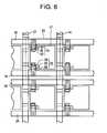
- FIG. 6The actual arrangement of the electrodes and the like corresponding to this circuit structure is shown in FIG. 6 . In FIG. 6 , however, the structure is simplified and shown in a 2 ⁇ 2 structure.
- FIG. 3the process for fabricating the TFTs of the liquid crystal display device according to the present invention is explained.
- a silicon oxide filmis deposited to a thickness of from 1,000 to 3,000 ⁇ as a blocking layer 51 by radio frequency (RF) magnetron sputtering on a glass substrate 50 made of an economical glass which resists to a temperature of 700° C. or less, e.g., about 600° C.
- the actual film depositionwas carried out in a 100% oxygen atmosphere at a film deposition temperature of 15° C., at an output of from 400 to 800 W, and a pressure of 0.5 Pa.
- the film deposition rate using a quartz or a single crystal silicon as the targetwas in the range of from 30 to 100 ⁇ /minute.
- a silicon filme.g. an amorphous silicon film, by LPCVD (low-pressure chemical vapor deposition), sputtering, or plasma-assisted CVD (PCVD).
- LPCVDlow-pressure chemical vapor deposition
- sputteringsputtering
- PCVDplasma-assisted CVD
- film depositionwas conducted at a temperature lower than the crystallization temperature by 100 to 200° C., i.e., in the range of from 450 to 550° C., e.g., at 530° C., by supplying disilane (Si 2 H 6 ) or trisilane (Si 3 H 8 ) to the CVD apparatus.
- the pressure inside the reaction chamberwas controlled to be in the range of from 30 to 300 Pa.
- the film deposition ratewas 50 to 250 ⁇ /minute.
- boronmay be supplied to 1 ⁇ 10 15 to 1 ⁇ 10 18 atoms ⁇ cm ⁇ 3 in the film as diborane during the film deposition to control the threshold voltage (V th ) of the N-TFT and that of the P-TFT to be approximately the same.
- film depositionwas conducted using a single crystal silicon as the target in an argon atmosphere having added therein from 20 to 80% of hydrogen, e.g., in a mixed gas atmosphere containing 20% of argon and 80% of hydrogen.
- the back pressure prior to sputteringwas controlled to 1 ⁇ 10 ⁇ 5 Pa or lower.
- the filmwas deposited at a film deposition temperature of 150° C., a frequency of 13.56 MHz, a sputter output of from 400 to 800 W, and a pressure of 0.5 Pa.
- the temperaturewas maintained, e.g., at 300° C., and monosilane (SiH 4 ) or disilane (Si 2 H 6 ) was used as the reacting gas.
- a high frequency electric powerwas applied at 13.56 MHz to the gas inside the PCVD apparatus to effect the film deposition.
- the films thus obtained by any of the foregoing processespreferably contain oxygen at a concentration of 5 ⁇ 10 21 cm ⁇ 3 or lower. If the oxygen concentration is too high, the film thus obtained would not crystallize. Accordingly, there would be required to elevate the thermal annealing temperature or to take a longer time for the thermal annealing. Too low an oxygen concentration, on the other hand, increases an off-state leak current due to a backlighting. Accordingly, the preferred range of the oxygen concentration was set in the range of from 4 ⁇ 10 19 to 4 ⁇ 10 21 atoms ⁇ cm ⁇ 3 .
- the hydrogen concentrationwas for example 4 ⁇ 10 22 atoms ⁇ cm ⁇ 3 , which accounts for 1% by atomic with respect to the silicon concentration of 4 ⁇ 10 22 atoms ⁇ cm ⁇ 3 .
- oxygen concentrationis 7 ⁇ 10 19 atoms ⁇ cm ⁇ 3 or less, preferably 1 ⁇ 10 19 atoms ⁇ cm ⁇ 3 or less and oxygen may be added selectively by ion-implantation to the channel forming regions of the TFT which constitute the pixel, to such an amount to give a concentration in the range of from 5 ⁇ 10 20 to 5 ⁇ 10 21 atoms ⁇ cm ⁇ 3 . Since no light was irradiated to the TFTs in the peripheral circuit, it was effective to impart thereto a higher carrier mobility while reducing the oxygen concentration in order to realize a high frequency operation.
- the amorphous silicon filmwas then heat-treated at a moderate temperature in the range of from 450 to 700° C. for a duration of from 12 to 70 hours in a non-oxidizing atmosphere. More specifically, the film was maintained at 600° C. under a hydrogen atmosphere. Since on the surface of the substrate was provided an amorphous silicon oxide layer under the silicon film, the whole structure was uniformly annealed because there was no nucleus present during the heat treatment.
- the processcan be explained as follows. That is, during the film deposition step, the film construction maintains the amorphous structure and the hydrogen is present as a mixture.
- the silicon filmthen undergoes phase transition from the amorphous structure to a structure having a higher degree of ordering by the annealing, and partly develops a crystallized portion. Particularly, the region which attains a relatively high degree of ordering at the film deposition of silicon tend to crystallize at this stage.
- the silicon bonding which bonds the silicon atoms each otherattracts a region to another. This effect can be observed by a laser Raman spectroscopy as a peak shifted to a lower frequency side as compared with the peak at 522 cm ⁇ 1 for a single crystal silicon.
- the apparent grain sizecan be calculated by the half width as 50 to 500 ⁇ , i.e., a size corresponding to that of a microcrystal, but in fact, the film has a semi-amorphous structure comprising a plurality of those highly crystalline regions yielding a cluster structure, and the clusters are anchored to each other by the bonding between the silicon atoms.
- the semi-amorphous filmyields, as a result, a state in which no grain boundary (referred to hereinafter as GB) exists. Since the carrier easily moves between the clusters via the anchoring, a carrier mobility far higher than that of a polycrystalline silicon having a distinct GB can be realized. More specifically, a hole mobility, ⁇ h, in the range of from 10 to 200 cm 2 /V ⁇ sec and an electron mobility, ⁇ e, in the range of from 15 to 300 cm 2 /V ⁇ sec, are achieved.
- FIG. 3 (A)a process for fabricating a region 22 for a P-TFT and a region 13 for an N-TFT is described.
- the silicon filmwas masked with a first photomask ⁇ 1 >, and subjected to photo-etching to obtain the region 22 (having a channel width of 20 ⁇ m) for the P-TFT on the right-hand side of the FIGURE and the region 13 for the N-TFT on the left-hand side of the FIGURE.
- a silicon oxide film as the gate insulator filmwas deposited to a thickness of from 500 to 2,000 ⁇ , e.g., to a thickness of 1,000 ⁇ .
- the conditions or the film depositionwere the same as those employed in depositing the silicon oxide film to give a blocking layer.
- a small amount of fluorinemay be added during the film deposition to fix sodium ions.
- the gate insulator filmwas deposited a silicon film doped with phosphorus at a concentration of from 1 ⁇ 10 21 to 5 ⁇ 10 21 atoms ⁇ cm ⁇ 3 , or a multilayered film composed of said silicon film doped with phosphorus, having provided thereon a layer of molybdenum (Mo), tungsten (W), MoSi 2 , or WSi 2 .
- Momolybdenum
- Wtungsten
- MoSi 2molybdenum
- WSi 2WSi 2
- a gate electrode 55 for the P-TFT, and a gate electrode 56 for the NTFTwere established, for example, by depositing first a 0.2 ⁇ m thick phosphorus(P)-doped silicon and a 0.3 ⁇ m thick molybdenum layer thereon, at a channel length of 10 ⁇ m.
- a photoresist 57was provided using a photomask ⁇ 3 >, and to a source 59 and a drain 58 for the P-TFT were added boron by ion implantation at a dose of from 1 ⁇ 10 15 to 5 ⁇ 10 15 cm ⁇ 2 . Then, as shown in FIG.
- a photoresist 61was provided using a photomask ⁇ 4 >, and to a source 64 and a drain 62 for the N-TFT was added phosphorus by ion implantation at a dose of from 1 ⁇ 10 15 to 5 ⁇ 10 15 cm ⁇ 2 .
- the processes abovewere carried out via a gate insulator film 54 .
- the silicon oxide on the silicon filmmay be removed utilizing the gate electrodes 55 and 56 as the masks, and then boron and phosphorus may be directly added to the silicon film by ion implantation.
- the structure thus obtainedwas re-annealed by heating at 600° C. for a duration of from 10 to 50 hours.
- the impurities in the source 59 and drain 58 of the P-TFT and those in the source 64 and drain 62 of the N-TFTwere activated to obtain P + and N + TFTs.
- Under the gate electrodes 55 and 56were provided channel forming regions 60 and 63 with a semi-amorphous semiconductor.
- a CTFTcan be obtained in a self-aligned method without elevating the temperature to 700° C. or higher.
- a substrate made of an expensive materialsuch as quartz, and therefore it can be seen that the process is suited for fabricating liquid crystal display devices of large pixels according to the present invention.
- the thermal annealing in this examplewas conducted twice, i.e., in the steps of fabricating the structures shown in FIGS. 3 (A) and 3 (D).
- the annealing at the step illustrated in FIG. 3 (A)may be omitted depending to the desired device characteristics, and the annealing at the step shown in FIG. 3 (D) can cover the total annealing. In this way it is possible to speed up the fabrication process.
- a silicon oxide filmwas deposited as an interlayer insulator 65 by the sputtering process mentioned hereinbefore.
- the method of depositing the silicon oxide filmis not restricted to a sputtering method, and there may be employed LPCVD, photo CVD, or normal pressure CVD.
- the silicon oxide filmwas deposited, e.g., to a thickness of from 0.2 to 0.6 ⁇ m, and on it was perforated an opening 66 for the electrode using a photomask ⁇ 5 >.
- the structurewas then wholly covered with aluminum by sputtering, and after providing lead portions 71 and 72 , as well as contacts 67 and 68 using a photomask ⁇ 6 >, the surface thereof was coated with a smoothening film of an organic resin 69 such as a transparent polyimide resin, and subjected again to perforation for the electrodes using a photomask ⁇ 7 >.
- an organic resin 69such as a transparent polyimide resin
- FIG. 3 (F)two insulated gate field effect thin film transistors were established in a complementary structure.
- an Indium Tin Oxide (ITO) filmby sputtering to thereby connect the TFTs with one of the transparent pixel electrodes of the liquid crystal display device.
- the ITO filmwas deposited in the temperature range from room temperature to 150° C., and then finished by annealing in oxygen or in atmosphere in the temperature range of from 200 to 400° C.
- the ITO filmwas then etched using a photomask ⁇ 8 > to form an electrode 70 .
- a structurecomprising a P-TFT 22 , an N-TFT 13 , and an electrode 70 made of a transparent electrically conductive film on a single glass substrate 50 .
- the resulting TFTyielded a mobility of 20 cm 2 /V ⁇ sec and a V th of ⁇ 5.9 V for the P-TFT, and a mobility of 40 cm 2 /V ⁇ sec and a V th of 5.0 V for the N-TFT.
- An N-TFT 13is assembled at the crossing of a first scanning line 15 and a data line 21 , and another pixel N-TFT is provided at the crossing of the first scanning line 15 with another data line 14 .
- a P-TFTis assembled at the crossing of a second scanning line 18 and a data line 21 .
- another pixel N-TFTis provided to the neighboring crossing of another first scanning line 16 and the data line 21 .
- the N-TFT 13is connected to the first scanning line 15 via a contact at the input terminal of the drain portion 64 , and the gate portion 56 is connected to the data line 21 established in a multilayered wiring structure.
- the output terminal of the source portion 62is connected to the pixel electrode 17 via a contact.
- the P-TFT 22is connected to the second scanning line 18 by the input terminal of the drain portion 58 via a contact, while the gate portion 55 is connected to the data line 21 , and the output terminal of the source portion 59 is connected to the pixel electrode 17 via a contact in the same manner as in the N-TFT.
- this manneris a single pixel established between (inner side) a pair of scanning lines 15 and 18 , with a pixel 23 comprising a transparent electrode and a CTFT pair.
- a 2 ⁇ 2 matrixcan be scaled up to give a large pixel liquid crystal display device comprising a 640 ⁇ 480 or a 1280 ⁇ 960 matrix.
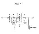
- FIGS. 4 and 5are given the circuit diagrams for the peripheral circuit of the X direction.
- FIG. 4illustrates the block function of the peripheral circuit being connected to a single wiring
- FIG. 5shows the circuit diagram for connecting the transistor in the unit.
- FIG. 5 (A)corresponds to the block 7 in FIG. 4
- FIG. 5 (B)shows the circuit structure of the TFT corresponding to the block 8 in FIG. 4 .
- the peripheral circuitis provided as a CMOS (complementary MOS) structure comprising an N-TFT 13 and a P-TFT 22 both fabricated in the same process as that employed for the switching device.
- CMOScomplementary MOS
- the substrate thus accomplished for use in the liquid crystal display devicewas laminated with the facing substrate by a known process, and an STN (super-twisted nematic) liquid crystal was injected between the substrates.
- the ICs 4were used for the other part of the peripheral circuit.
- the ICs 4were connected with each of the wirings for the Y direction on the substrate by a TAB process. Thus was completed a liquid crystal display device according to the present invention.
- peripheral circuit for the X directionwas fabricated as TFTs following the same process used for the switching device, while leaving over the rest of the peripheral circuit as ICs having connected to the wirings of the Y direction.
- the present inventionis not only limited to this construction, and the portion which can be more easily fabricated into TFTs can be selected depending on the yield and the problems related to the process technology at the fabrication of the TFTs.
- a semiconductor film which comprises a semiconductor(amorphous silicon semiconductor in this Example) was formed extending over a display area and a peripheral circuit portion and subsequently the semiconductor (amorphous silicon semiconductor in this Example) is annealed into semi-amorphous or semi-crystal semiconductor.
- the semi-amorphous semiconductoryields a mobility ten times as high as, or even higher than that of the TFT using a conventional non-single crystal semiconductor.
- the TFT according to the present inventionis well applicable to the peripheral circuits in which a rapid response is required, without subjecting the TFTs in the peripheral circuit portion to a special crystallization treatment which was requisite in the conventional TFTs; as a result, the TFTs for the peripheral circuit portion could be fabricated by the same process utilized for fabricating an active device of the display area, as described above.
- FIG. 7is given a schematic view of a liquid crystal display device according to another embodiment of the present invention.
- the basic circuits and the likeare the same as those employed in the liquid crystal display device described in Example 1.
- the peripheral circuit connected to the wirings for the Y directionis constructed with ICs 4 , and the ICs 4 are directly provided on the substrate by a COG method.
- the pad electrodes of the ICs 4can be connected with the wirings of the Y direction at a narrower interval by the use of a COG method instead of the TAB method.
- the process of the present exampleenables a finer display pixel design.
- the ICsare provided on the substrate, the total volume of the display device remains almost unchanged to give a thinner liquid crystal display device.
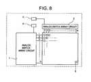
- a liquid crystal display device having an m ⁇ n circuit structureis described below.
- the peripheral circuit portionsa means for supplying a signal to wirings of the X direction
- an analog switch array circuit portion 1is fabricated as TFTs in the same process as that used for fabricating the active device provided to a pixel 6 .
- an analog switch array circuit portion 2 in the peripheral circuit portion(a means for supplying a signal to wirings of the Y direction) connected to the wirings of the Y direction is also fabricated as TFTs, while providing the rest of the peripheral circuit portion by making them into ICs 4 having connected to a substrate using a COG method.
- the peripheral circuit portion provided as TFTsis in a CTFT structure (complementary structure) similar to the active device established to the pixels.
- FIG. 6is provided the actual arrangement of the electrodes and the like corresponding to the circuit structure described above. However, the portion shown in FIG. 6 corresponds to a 2 ⁇ 2 matrix for the sake of simplicity.
- Electrodes, TFTs, wirings, and the likewere formed on a single substrate in the same fabrication process as that used in Example 1.
- the switching devicee.g. TFTs 13 and 22 in FIG. 6
- a part of the peripheral circuitswere fabricated in TFTs on the same substrate.
- This substratewas laminated with the facing substrate and an STN liquid crystal was injected between the substrates in the same manner as in Example 1.
- the remaining peripheral circuitwas established as ICs 4 .
- the ICs 4were connected with each of the wirings of the X and Y directions by a COG method. To the ICs 4 was connected each of the connection leads for power supply and data input, but there was no FPC attached all over one edge of the substrate for the connection. The reliability of the liquid crystal display device was increased by thus reducing the number of connections.
- liquid crystal display deviceIn the liquid crystal display device described in the present Example, only the analog switch array circuit portion 1 among the peripheral circuit of the X direction and the analog switch array circuit portion 2 among the peripheral circuit of the Y direction were fabricated into complementary TFTs in the same process as that used for fabricating a switching device. The remaining peripheral circuit portion was provided as the ICs 4 .
- a liquid crystal display deviceis not restricted to this structure and the portion which can be more easily fabricated as TFTs can be selected and fabricated as TFTs, depending on the yield and the problems related to the process technology at the fabrication thereof.
- a semi-amorphous semiconductorwas used for the semiconductor film.
- the TFT according to the present inventionis well applicable to peripheral circuits in which a rapid response is required, without subjecting the TFTs in the peripheral circuit portion to a special crystallization treatment which was requisite in the conventional TFTs; as a result, the TFTs for the peripheral circuit portion could be fabricated by the same process utilized for fabricating an active device.
- the peripheral circuit portion composed of ICs 4comprises ICs having directly established on the substrate by a COG method.
- the ICs 4are divided into two portions, and one of them is provided at the upper portion of the substrate and the other is provided at the lower portion of the substrate.
- the pad electrodes of the ICs 4 and the wirings of the Y directioncan be connected at a narrower interval as compared with the case in which the ICs are provided only on one side of the substrate.
- This structurecan be therefore characterized by a finer display pixel design.
- the ICsare directly bonded on the substrate, the structure can be realized with a negligible change in volume and hence enables a thinner liquid crystal display device.
- the TFTs of the active devicewere each fabricated into a CMOS structure.
- this structureis not requisite and modifications such as constructing the structure with only N-TFTs or with only P-TFTs are also acceptable. In these cases, however, the number of the devices in the peripheral circuit would be increased.
- the position at which the TFTs are establishedcan be varied. That is, the TFT need not be provided only to one side, i.e., only to either of the sides connected to the wirings of the X direction and the Y direction, but there may be also provided a second TFT on the other side to connect the TFTs in turns to halve the TFT density.
- Such a structurerealizes an increase in the production yield.
- the present inventionprovides a fine and precise liquid crystal display by overcoming the problems ascribed to the limitations related to the technological difficulty in the peripheral connections. Furthermore, the reliability on the connections is improved, since unnecessary connections between the outer peripheral circuits and the wirings along the X and Y directions are minimized.
- the area occupation of the display substrate itselfis reduced, since only a part of the peripheral circuits are fabricated into a TFT. It also allows a more freely designed substrate having a shape and dimension according to the requirements. Further it is possible to reduce the production cost, since the problems related to the production of the TFTs can be avoided while making those portions having a higher production yield into TFTs.
- TFTsfor the peripheral circuits are readily fabricated simultaneously utilizing the fabrication process for the active devices without any additional special treatments.
- the liquid crystal display deviceprovides a stable display because it operates without floating the liquid crystal potential. Furthermore, since the drive capacity of the CTFTs which function as the active devices is high, the operational margin is increased. Since the peripheral driving circuit can be further simplified, it results in a more compact display device which is produced at a lower production cost. A high driving capacity can be realized with three signal lines and counter electrodes using a very simple signal. It is also possible to increase the switching rate. Even when a part of the TFTs should get out of order, a compensation function works to a certain degree.
- the carrier mobilityincreases to 10 times or more than that of a TFT using an amorphous silicon
- the size of the TFTcan be minimized and two TFTs can be connected to a single pixel without decreasing the aperture ratio.
- the advantages enumerated abovecan be realized by only using twice more the photomasks as compared with a conventional process in which only N-TFTs are used.
Landscapes
- Liquid Crystal (AREA)
- Thin Film Transistor (AREA)
Abstract
Description
This application is a Divisional of application Ser. No. 08/962,600 filed Oct. 31, 1997 now U.S. Pat. No. 6,306,213; which itself is a Divisional of Ser. No. 08/231,644 filed Apr. 22, 1994, now U.S. Pat. No. 5,849,601; which itself is a Continuation of Ser. No. 08/217,211 filed Mar. 24, 1994, abandoned; which is a Continuation of Ser. No. 07/811,063 filed Feb. 20, 1991, abandoned; which is a Continuation-in-Part of Ser. No. 08/293,201 filed Aug. 19, 1994, now U.S. Pat. No. 5,614,732; which is a Continuation of Ser. No. 07/967,564 filed Oct. 28, 1992, abandoned; which is a Continuation of Ser. No. 07/673,821 filed Mar. 21, 1991, abandoned.
1. Field of the Invention
The present invention relates to an electro-optical device which comprises thin film transistors (referred to hereinafter as TFTs) and to a method for manufacturing such a device.
2. Description of the Prior Art
More attention is now paid to flat displays than to CRTs (cathode ray tubes) for use in office automation (OA) machines and the like, and particularly, there is an increasing demand for large-area display devices. There is also an active and rapid development in the application field of flat displays such as wall television (TV) sets. Furthermore, there are demands for color flat displays and finer display images.
A liquid crystal display device is known as a representative example of a flat display. A liquid crystal display device comprises a pair of glass substrates having incorporated therebetween a liquid crystal composition together with electrodes, and the images are displayed by the change of state of the liquid crystal composition upon application of an electric field thereto. The liquid crystal cells may be driven by the use of a TFT or other switching devices, or by making it into a simple matrix structure. In any case, a driver circuit is established at the periphery of a display to supply signals for driving liquid crystals to column lines (extending in Y direction) and row lines (extending in X direction).
The driver circuit is generally composed of a single crystal silicon MOS integrated circuit (IC). The IC is provided with pad electrodes, each corresponding to each of the display electrodes, and a printed circuit board is incorporated between the pad and the display electrodes to connect first the pad electrode of the IC with the printed circuit board and then the printed circuit board with the display. The printed circuit board, which in general is made of an insulator board made from materials such as a glass fiber-reinforced epoxy resin or a paper filled epoxy resin, or of a flexible plastic board, requires an area equivalent to or even larger than the display area. Similarly, the volume thereof should have to be made considerably large.
Thus, because of the construction as described hereinabove, a conventional display suffers problems as follows:
- (1) A superfine display cannot be realized. Since each of the wirings of the display electrodes for the X direction and the Y direction of the matrix, or the source (drain) wirings or the gate wirings should be connected individually to each of the contacts on the printed board, the minimum distance between the connecting portions technologically achievable by the up-to-date surface mounting technology is limited to a certain length;
- (2) A display device as a whole occupies a large area and volume. A display device comprises indispensable parts in addition to the display itself, inclusive of the printed circuit board, the ICs, and the connecting wirings, which require an area and volume about several times as large as those of the display alone; and
- (3) The connections are of low reliability. Quite a large number of connections should be established between the main display and the printed circuit board, as well as between the printed circuit board and the ICs; moreover, not a small weight is casted on the connecting portions.
As a means to overcome the foregoing problems, there is proposed, particularly in a display device comprising an active matrix as the switching device, to construct a display device comprising the active device and the peripheral circuits on a same substrate using TFTs rather than semiconductor chips. Such a construction indeed solves the three problems mentioned hereinabove, however, it newly develops problems as follows:
- (4) The production yield of the display is low. Since the peripheral circuits also are made from TFTs, the number of the devices to be fabricated on the same substrate is increased and hence the production yield of the TFT is lowered;
- (5) The production cost is increased. Since the peripheral circuit portion comprises a very complicated device structure, the circuit pattern accordingly becomes complicated and hence the cost increases. Furthermore, with the increase in the multilayered wiring portion, an increase in process steps as well as a decrease in the production yield of the TFTs occur; and
- (6) It requires a treatment at a high temperature and hence the use of an expensive quartz substrate becomes requisite. Since a quick response is required to the transistors which constitute the peripheral circuit, the semiconductor layer should be treated at a high temperature to obtain a polycrystalline layer to be used as the transistors.
An object of the present invention is to overcome the six problems mentioned above by taking balance among them and to provide a more economical electro-optical device at a high yield.
This and other objects of the present invention have been attained by an electro-optical device comprising a pair of substrates and an electro-optical modulating layer having sandwiched therebetween, said pair of substrates consisting of a first substrate having provided thereon thin film transistors and matrix lines comprising a plurality of gate wires (extending e.g. in Y direction) and a plurality of source (drain) wires (extending e.g. in X direction), and a second substrate facing the first substrate, wherein, among the peripheral circuits being connected to the matrix lines, only one direction side of said peripheral circuits is constructed from thin film semiconductor devices fabricated by the same process utilized for the thin film transistors, and the rest of the peripheral circuits is constructed from semiconductor chips. The electro-optical modulating layer may comprise a liquid crystal.
In the electro-optical device according to the present invention, the peripheral circuit only on one side is fabricated as TFTs. In such a manner, a general use economical ICs can be utilized on one side, while fabricating the side comprising peripheral circuits which are not commercially available or which are costly, as TFTs.
Furthermore, by making only one side into TFTs, the number of the TFTs in the peripheral circuit portion can be considerably reduced. For example, the number of the TFTs can be halved in case the peripheral circuits for the X and the Y directions have the same function. Thus, the production yield of a TFT on the same substrate is increased by two times in a simple calculation.
According to another embodiment of the present invention, there is provided an electro-optical device comprising a first substrate having provided thereon a pixel matrix furnished with complementary TFTs and matrix lines comprising a plurality of gate wires (extending e.g. in Y direction) and a plurality of source (drain) wires (extending e.g. in X direction), said first substrate making a pair with a second substrate faced thereto and an electro-optical modulating layer having supported between the pair of substrates, characterized by that at least a part of the peripheral circuits being connected to the matrix lines is fabricated into complementary TFTs similar in structure of the active matrix (e.g. the complementary TFTs of the pixel matrix) and being fabricated also in a same process as that of the active matrix, and that the rest of the peripheral circuits are constructed by semiconductor chips, said peripheral circuits being connected to the X or Y direction matrix wires having established on the first substrate. The electro-optical modulating layer may comprise a liquid crystal.
More precisely, the electro-optical device according to the present invention is characterized by that the peripheral circuit is not wholly fabricated into TFTs, but only those portions having a simple device structure, or those composed of a small number of devices, or those comprising an IC not easily available commercially, or those comprising an expensive IC, are fabricated as TFTs. It is therefore an object of the present invention to increase the production yield and to reduce the production cost of an electro-optical device.
Accordingly, by fabricating a part of the peripheral circuits as TFTs, the number of external ICs is reduced and therefore the production cost is reduced.
Furthermore, by fabricating the peripheral circuits and the active matrix in the same process to give complementary TFTs (CTFTs), the pixel driving capacity is increased and a redundancy is imparted to the peripheral circuit. Hence it is possible to drive the electro-optical device with a greater allowance.
If the peripheral circuits were to be wholly fabricated into TFTs, the device requires extension of the display substrate along both of the X and Y directions. This inevitably leads to an unfavorable increase in the total occupancy area. In contrast, if only a part of the peripheral circuits were to be fabricated into TFTs, it results in a slight increase of the substrate which can be readily accommodated to the outer dimension of the computers and other apparatuses to which the electro-optical device is assembled. Thus, there is provided an electro-optical device having a small occupancy area and volume.
A high technology is required to fabricate the complicated portions in the peripheral circuit as TFTs. For example, a device structure which requires a multilayered wiring, or a portion having a function as an amplifier can be mentioned as those particular portions. However, if the peripheral circuit were to be partially made into TFTs by replacing only the simple device structures and portions of simple function with TFTs while using the conventional ICs for the portions in which high technology is required, an electro-optical device can be realized at reduced cost with a high yield.
Furthermore, a partial adoption of TFTs considerably reduces the number of TFTs within the peripheral circuit portion. In a simple calculation, it can be seen that the number of the TFTs can be reduced to a half if the function of the TFTs for the X direction and the Y direction were the same. It is possible, by reducing the number of devices to be fabricated as TFTs, to increase the production yield of the substrate. In addition, there is provided a low cost electro-optical device reduced both in the area of the substrate and in volume.
In an electro-optical device according to an embodiment of the present invention, a single pixel may be constructed by connecting two or more CTFTs with a pixel. Otherwise, a single pixel may be divided into two or more pixels, and to each of the divided pixels may be connected one or more CTFTs.
The ICs of the residual peripheral circuit portions which are not fabricated as TFTs are connected with the substrate by a surface mounting technology (SMT) such as a Chip on Glass (COG) process which comprises directly mounting the IC chips on a substrate and connecting them with each of the connecting terminals, and a Tape Automated Bonding (TAB) process which comprises mounting each of the IC chips on a flexible support made of an organic resin, and then connecting the resin support with the display substrate.
It is further possible to fabricate the semiconductor layers of the TFTs at a lower temperature and yet to realize quick response TFTs having a considerably increased carrier mobility by taking advantage of, instead of the conventional polycrystalline or amorphous semiconductors, a semi-amorphous semiconductor which is based on a novel concept.
The semi-amorphous semiconductor can be obtained by applying a heat treatment to crystallize a thin film having deposited by processes such as low-pressure chemical vapor deposition (LPCVD), sputtering, plasma-assisted chemical vapor deposition (PCVD), and the like. The process for fabricating a semi-amorphous semiconductor film is described below referring to the sputtering process as an example.
In depositing a film by sputtering from a single crystal target of a silicon semiconductor under a mixed gas atmosphere comprising hydrogen and argon, the heavy argon atoms strike the surface of the silicon target to release free silicon atoms. The free silicon atoms thus released from the target then travel to the substrate on which the film is to be deposited, accompanied by clusters composed of several tens to several millions of silicon atoms. During their travel in the sputtering chamber, hydrogen atoms come to bond with the dangling bonds of the silicon atoms located at the outer periphery of the clusters, and these clusters comprising the silicon-hydrogen bonding are maintained to the surface of the substrate to deposit as a relatively ordered region. Thus, a highly ordered film comprising a mixture of amorphous silicon and clusters accompanied by Si—H bondings on the periphery is realized on the surface of the substrate. By further heat treating the deposited film in the temperature range of from 450 to 700° C. in a non-oxidizing atmosphere, the Si—H bondings on the outer periphery of the clusters react with each other to yield Si—Si bondings. The Si—Si bondings thus obtained exert a strong attractive force to each other. At the same time, however, the clusters in their highly ordered state are susceptible to undergo phase transition to attain a more ordered state, i.e., a crystallized state. Thus, because the Si—Si bondings in the neighboring clusters attract each other, the resulting crystals suffer lattice distortion which can be observed by laser Raman spectroscopy as a peak deviated in position to the lower frequency side from the 520 cm−1which corresponds to the peak of a single crystal of silicon.
Furthermore, since the Si—Si bondings between the neighboring clusters cause anchoring (connecting) effects, the energy band in each cluster is electrically connected with that of the neighboring cluster through the anchored locations. Accordingly, since there is no grain boundaries as in the conventional polycrystalline silicon which function as a barrier to the carriers, a carrier mobility as high as in the range of from 10 to 200 cm2/V·sec can be obtained. That is, the semi-amorphous semiconductor defined above is apparently crystalline, however, if viewed from the electrical properties, there can be assumed a state substantially free from grain boundaries. If the annealing of a silicon semiconductor were to be effected at a temperature as high as 1000° C. or over, instead of a moderate annealing in the temperature range of from 450 to 700° C. as referred hereinbefore, the crystallization naturally would induce crystal growth to precipitate oxygen and the like at the grain boundaries and would develop a barrier. The resulting material is then a polycrystalline material comprising single crystals and grain boundaries.
In the semi-amorphous semiconductors, the carrier mobility increases with elevating degree of anchoring. To enhance carrier mobility and to allow the crystallization to take place at a temperature lower than 600° C., the oxygen content of the film should be controlled to 7×1019cm−3or lower, preferably, to 1×1019cm−3or lower.
FIGS.3(a)-3(d) are a schematic representation illustrating the fabrication process of a TFT according to an embodiment of the present invention;
FIGS.5(a) and5(b) are a schematic representation of a connection of transistors of a peripheral circuit according to a liquid crystal display device of an embodiment of the present invention;
The present invention is described in further detail below referring to non-limiting examples.
Referring toFIG. 1 , a liquid crystal display device having an m×n circuit structure is described. InFIG. 2 is also given the outer appearance of the liquid crystal display device. InFIG. 1 , a shift register circuit portion1 (a means for supplying a signal to a wiring of the X direction) being connected to a wiring of the X direction is solely fabricated asTFTs 5 in a similar manner as an active device provided to apixel 6, and a peripheral circuit portion (a means for supplying a signal to a wiring of the Y direction) connected to a wiring of the Y direction is provided asICs 4 which is connected to the substrate by TAB. The thin film transistors provided in thepixel 6 as the active device and thethin film transistors 5 constituting the shiftregister circuit portion 1 are provided on a single substrate.
The actual arrangement of the electrodes and the like corresponding to this circuit structure is shown in FIG.6. InFIG. 6 , however, the structure is simplified and shown in a 2×2 structure.
Referring toFIG. 3 , the process for fabricating the TFTs of the liquid crystal display device according to the present invention is explained. In FIG.3(A), a silicon oxide film is deposited to a thickness of from 1,000 to 3,000 Å as ablocking layer 51 by radio frequency (RF) magnetron sputtering on aglass substrate 50 made of an economical glass which resists to a temperature of 700° C. or less, e.g., about 600° C. The actual film deposition was carried out in a 100% oxygen atmosphere at a film deposition temperature of 15° C., at an output of from 400 to 800 W, and a pressure of 0.5 Pa. The film deposition rate using a quartz or a single crystal silicon as the target was in the range of from 30 to 100 Å/minute.
On the silicon oxide film thus obtained was further deposited a silicon film, e.g. an amorphous silicon film, by LPCVD (low-pressure chemical vapor deposition), sputtering, or plasma-assisted CVD (PCVD).
In case of the LPCVD process, film deposition was conducted at a temperature lower than the crystallization temperature by 100 to 200° C., i.e., in the range of from 450 to 550° C., e.g., at 530° C., by supplying disilane (Si2H6) or trisilane (Si3H8) to the CVD apparatus. The pressure inside the reaction chamber was controlled to be in the range of from 30 to 300 Pa. The film deposition rate was 50 to 250 Å/minute. Furthermore, optionally boron may be supplied to 1×10¹⁵to 1×10¹⁸atoms·cm−3in the film as diborane during the film deposition to control the threshold voltage (Vth) of the N-TFT and that of the P-TFT to be approximately the same.
In case of sputtering, film deposition was conducted using a single crystal silicon as the target in an argon atmosphere having added therein from 20 to 80% of hydrogen, e.g., in a mixed gas atmosphere containing 20% of argon and 80% of hydrogen. The back pressure prior to sputtering was controlled to 1×10⁻⁵Pa or lower. The film was deposited at a film deposition temperature of 150° C., a frequency of 13.56 MHz, a sputter output of from 400 to 800 W, and a pressure of 0.5 Pa.
In case of the deposition of a silicon film by a PCVD process, the temperature was maintained, e.g., at 300° C., and monosilane (SiH4) or disilane (Si2H6) was used as the reacting gas. A high frequency electric power was applied at 13.56 MHz to the gas inside the PCVD apparatus to effect the film deposition.
The films thus obtained by any of the foregoing processes preferably contain oxygen at a concentration of 5×1021cm−3or lower. If the oxygen concentration is too high, the film thus obtained would not crystallize. Accordingly, there would be required to elevate the thermal annealing temperature or to take a longer time for the thermal annealing. Too low an oxygen concentration, on the other hand, increases an off-state leak current due to a backlighting. Accordingly, the preferred range of the oxygen concentration was set in the range of from 4×10¹⁹to 4×10²¹atoms·cm−3. The hydrogen concentration was for example 4×10²²atoms·cm−3, which accounts for 1% by atomic with respect to the silicon concentration of 4×10²²atoms·cm−3. To enhance crystallization of the source and drain portions, oxygen concentration is 7×10¹⁹atoms·cm−3or less, preferably 1×10¹⁹atoms·cm−3or less and oxygen may be added selectively by ion-implantation to the channel forming regions of the TFT which constitute the pixel, to such an amount to give a concentration in the range of from 5×10²⁰to 5×10²¹atoms·cm−3. Since no light was irradiated to the TFTs in the peripheral circuit, it was effective to impart thereto a higher carrier mobility while reducing the oxygen concentration in order to realize a high frequency operation.
After the amorphous silicon film was deposited at a thickness of from 500 to 5,000 Å, e.g., at a thickness of 1,500 Å, the amorphous silicon film was then heat-treated at a moderate temperature in the range of from 450 to 700° C. for a duration of from 12 to 70 hours in a non-oxidizing atmosphere. More specifically, the film was maintained at 600° C. under a hydrogen atmosphere. Since on the surface of the substrate was provided an amorphous silicon oxide layer under the silicon film, the whole structure was uniformly annealed because there was no nucleus present during the heat treatment.
The process can be explained as follows. That is, during the film deposition step, the film construction maintains the amorphous structure and the hydrogen is present as a mixture. The silicon film then undergoes phase transition from the amorphous structure to a structure having a higher degree of ordering by the annealing, and partly develops a crystallized portion. Particularly, the region which attains a relatively high degree of ordering at the film deposition of silicon tend to crystallize at this stage. However, the silicon bonding which bonds the silicon atoms each other attracts a region to another. This effect can be observed by a laser Raman spectroscopy as a peak shifted to a lower frequency side as compared with the peak at 522 cm−1for a single crystal silicon. The apparent grain size can be calculated by the half width as 50 to 500 Å, i.e., a size corresponding to that of a microcrystal, but in fact, the film has a semi-amorphous structure comprising a plurality of those highly crystalline regions yielding a cluster structure, and the clusters are anchored to each other by the bonding between the silicon atoms.
The semi-amorphous film yields, as a result, a state in which no grain boundary (referred to hereinafter as GB) exists. Since the carrier easily moves between the clusters via the anchoring, a carrier mobility far higher than that of a polycrystalline silicon having a distinct GB can be realized. More specifically, a hole mobility, μh, in the range of from 10 to 200 cm2/V·sec and an electron mobility, μe, in the range of from 15 to 300 cm2/V·sec, are achieved.
On the other hand, if a high temperature annealing in the temperature range of from 900 to 1200° C. were to be applied in the place of a moderate temperature annealing as described hereinabove, impurities undergo a solid phase growth from the nuclei and segregate in the film. This results in the high concentration of oxygen, carbon, nitrogen, and other impurities at the GB into a barrier. Thus, despite the high mobility within a single crystal, the carrier is interfered at its transfer from a crystal to another by the barrier at the GB. In practice, it is quite difficult to attain a mobility higher than or equal to 10 cm2/V·sec with a polycrystalline silicon at the present. Thus, in the liquid crystal display device according to the present invention, a semi-amorphous or a semi-crystalline structured silicon semiconductor is utilized.
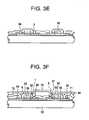
Referring to FIG.3(A), a process for fabricating aregion 22 for a P-TFT and aregion 13 for an N-TFT is described. The silicon film was masked with a first photomask <1>, and subjected to photo-etching to obtain the region22 (having a channel width of 20 μm) for the P-TFT on the right-hand side of the FIGURE and theregion 13 for the N-TFT on the left-hand side of the FIGURE.
On the resulting structure was deposited a silicon oxide film as the gate insulator film to a thickness of from 500 to 2,000 Å, e.g., to a thickness of 1,000 Å. The conditions or the film deposition were the same as those employed in depositing the silicon oxide film to give a blocking layer. Alternatively, a small amount of fluorine may be added during the film deposition to fix sodium ions.
Further on the gate insulator film was deposited a silicon film doped with phosphorus at a concentration of from 1×10²¹to 5×10²¹atoms·cm−3, or a multilayered film composed of said silicon film doped with phosphorus, having provided thereon a layer of molybdenum (Mo), tungsten (W), MoSi2, or WSi2. The resulting film was patterned using a second photomask <2> to obtain a structure as shown in FIG.3(B). Then, agate electrode 55 for the P-TFT, and agate electrode 56 for the NTFT were established, for example, by depositing first a 0.2 μm thick phosphorus(P)-doped silicon and a 0.3 μm thick molybdenum layer thereon, at a channel length of 10 μm. Referring to FIG.3(C), aphotoresist 57 was provided using a photomask <3>, and to asource 59 and adrain 58 for the P-TFT were added boron by ion implantation at a dose of from 1×10¹⁵to 5×1015cm−2. Then, as shown in FIG.3(D), a photoresist61 was provided using a photomask <4>, and to asource 64 and adrain 62 for the N-TFT was added phosphorus by ion implantation at a dose of from 1×10¹⁵to 5×1015cm−2. The processes above were carried out via agate insulator film 54. However, referring to FIG.3(B), the silicon oxide on the silicon film may be removed utilizing thegate electrodes
The structure thus obtained was re-annealed by heating at 600° C. for a duration of from 10 to 50 hours. The impurities in thesource 59 and drain58 of the P-TFT and those in thesource 64 and drain62 of the N-TFT were activated to obtain P+ and N+ TFTs. Under thegate electrodes channel forming regions
According to the process for fabricating a liquid crystal display device of the present invention as described hereinabove, a CTFT can be obtained in a self-aligned method without elevating the temperature to 700° C. or higher. Thus, there is no need to use a substrate made of an expensive material such as quartz, and therefore it can be seen that the process is suited for fabricating liquid crystal display devices of large pixels according to the present invention.
The thermal annealing in this example was conducted twice, i.e., in the steps of fabricating the structures shown in FIGS.3(A) and3(D). However, the annealing at the step illustrated in FIG.3(A) may be omitted depending to the desired device characteristics, and the annealing at the step shown in FIG.3(D) can cover the total annealing. In this way it is possible to speed up the fabrication process.
Referring to FIG.3(E), a silicon oxide film was deposited as aninterlayer insulator 65 by the sputtering process mentioned hereinbefore. The method of depositing the silicon oxide film is not restricted to a sputtering method, and there may be employed LPCVD, photo CVD, or normal pressure CVD. The silicon oxide film was deposited, e.g., to a thickness of from 0.2 to 0.6 μm, and on it was perforated anopening 66 for the electrode using a photomask <5>. The structure was then wholly covered with aluminum by sputtering, and after providinglead portions contacts 67 and68 using a photomask <6>, the surface thereof was coated with a smoothening film of anorganic resin 69 such as a transparent polyimide resin, and subjected again to perforation for the electrodes using a photomask <7>.
As shown in FIG.3(F), two insulated gate field effect thin film transistors were established in a complementary structure. To the output terminal thereof was provided an Indium Tin Oxide (ITO) film by sputtering to thereby connect the TFTs with one of the transparent pixel electrodes of the liquid crystal display device. In this case, the ITO film was deposited in the temperature range from room temperature to 150° C., and then finished by annealing in oxygen or in atmosphere in the temperature range of from 200 to 400° C. The ITO film was then etched using a photomask <8> to form anelectrode 70. Thus was finally obtained a structure comprising a P-TFT 22, an N-TFT 13, and anelectrode 70 made of a transparent electrically conductive film on asingle glass substrate 50. The resulting TFT yielded a mobility of 20 cm2/V·sec and a Vthof −5.9 V for the P-TFT, and a mobility of 40 cm2/V·sec and a Vthof 5.0 V for the N-TFT.
Referring toFIG. 6 , the arrangement of electrodes and the like in the pixel portion of the liquid crystal display device is explained. An N-TFT 13 is assembled at the crossing of afirst scanning line 15 and adata line 21, and another pixel N-TFT is provided at the crossing of thefirst scanning line 15 with anotherdata line 14. On the other hand, a P-TFT is assembled at the crossing of asecond scanning line 18 and adata line 21. Further, to the neighboring crossing of anotherfirst scanning line 16 and thedata line 21 is provided another pixel N-TFT. Thus is accomplished a matrix structure using CTFTs. The N-TFT 13 is connected to thefirst scanning line 15 via a contact at the input terminal of thedrain portion 64, and thegate portion 56 is connected to thedata line 21 established in a multilayered wiring structure. The output terminal of thesource portion 62 is connected to thepixel electrode 17 via a contact.
The P-TFT 22, on the other hand, is connected to thesecond scanning line 18 by the input terminal of thedrain portion 58 via a contact, while thegate portion 55 is connected to thedata line 21, and the output terminal of thesource portion 59 is connected to thepixel electrode 17 via a contact in the same manner as in the N-TFT. In this manner is a single pixel established between (inner side) a pair ofscanning lines pixel 23 comprising a transparent electrode and a CTFT pair. By extending this basic pixel structure in four directions, a 2×2 matrix can be scaled up to give a large pixel liquid crystal display device comprising a 640×480 or a 1280×960 matrix.
InFIGS. 4 and 5 are given the circuit diagrams for the peripheral circuit of the X direction.FIG. 4 illustrates the block function of the peripheral circuit being connected to a single wiring, andFIG. 5 shows the circuit diagram for connecting the transistor in the unit. FIG.5(A) corresponds to theblock 7 inFIG. 4 , and FIG.5(B) shows the circuit structure of the TFT corresponding to theblock 8 in FIG.4. It can be seen therefrom that the peripheral circuit is provided as a CMOS (complementary MOS) structure comprising an N-TFT 13 and a P-TFT 22 both fabricated in the same process as that employed for the switching device.
The substrate thus accomplished for use in the liquid crystal display device was laminated with the facing substrate by a known process, and an STN (super-twisted nematic) liquid crystal was injected between the substrates. TheICs 4 were used for the other part of the peripheral circuit. TheICs 4 were connected with each of the wirings for the Y direction on the substrate by a TAB process. Thus was completed a liquid crystal display device according to the present invention.
In the embodiment explained in the Example, only the peripheral circuit for the X direction was fabricated as TFTs following the same process used for the switching device, while leaving over the rest of the peripheral circuit as ICs having connected to the wirings of the Y direction. The present invention, however, is not only limited to this construction, and the portion which can be more easily fabricated into TFTs can be selected depending on the yield and the problems related to the process technology at the fabrication of the TFTs.
As described above, on the substrate a semiconductor film which comprises a semiconductor (amorphous silicon semiconductor in this Example) was formed extending over a display area and a peripheral circuit portion and subsequently the semiconductor (amorphous silicon semiconductor in this Example) is annealed into semi-amorphous or semi-crystal semiconductor. The semi-amorphous semiconductor yields a mobility ten times as high as, or even higher than that of the TFT using a conventional non-single crystal semiconductor. Thus, the TFT according to the present invention is well applicable to the peripheral circuits in which a rapid response is required, without subjecting the TFTs in the peripheral circuit portion to a special crystallization treatment which was requisite in the conventional TFTs; as a result, the TFTs for the peripheral circuit portion could be fabricated by the same process utilized for fabricating an active device of the display area, as described above.
InFIG. 7 is given a schematic view of a liquid crystal display device according to another embodiment of the present invention. The basic circuits and the like are the same as those employed in the liquid crystal display device described in Example 1. Referring toFIG. 7 , the peripheral circuit connected to the wirings for the Y direction is constructed withICs 4, and theICs 4 are directly provided on the substrate by a COG method.
The pad electrodes of theICs 4 can be connected with the wirings of the Y direction at a narrower interval by the use of a COG method instead of the TAB method. Thus, the process of the present example enables a finer display pixel design. Furthermore, since the ICs are provided on the substrate, the total volume of the display device remains almost unchanged to give a thinner liquid crystal display device.
Referring toFIG. 8 , a liquid crystal display device having an m×n circuit structure is described below. Among the peripheral circuit portions (a means for supplying a signal to wirings of the X direction) connected to the wirings of the X direction, only an analog switcharray circuit portion 1 is fabricated as TFTs in the same process as that used for fabricating the active device provided to apixel 6. Furthermore, only an analog switcharray circuit portion 2 in the peripheral circuit portion (a means for supplying a signal to wirings of the Y direction) connected to the wirings of the Y direction is also fabricated as TFTs, while providing the rest of the peripheral circuit portion by making them intoICs 4 having connected to a substrate using a COG method. The peripheral circuit portion provided as TFTs is in a CTFT structure (complementary structure) similar to the active device established to the pixels.
InFIG. 6 is provided the actual arrangement of the electrodes and the like corresponding to the circuit structure described above. However, the portion shown inFIG. 6 corresponds to a 2×2 matrix for the sake of simplicity.
Electrodes, TFTs, wirings, and the like were formed on a single substrate in the same fabrication process as that used in Example 1. In this process, the switching device (e.g. TFTs13 and22 inFIG. 6 ) and a part of the peripheral circuits were fabricated in TFTs on the same substrate. This substrate was laminated with the facing substrate and an STN liquid crystal was injected between the substrates in the same manner as in Example 1. The remaining peripheral circuit was established asICs 4. TheICs 4 were connected with each of the wirings of the X and Y directions by a COG method. To theICs 4 was connected each of the connection leads for power supply and data input, but there was no FPC attached all over one edge of the substrate for the connection. The reliability of the liquid crystal display device was increased by thus reducing the number of connections.
In the liquid crystal display device described in the present Example, only the analog switcharray circuit portion 1 among the peripheral circuit of the X direction and the analog switcharray circuit portion 2 among the peripheral circuit of the Y direction were fabricated into complementary TFTs in the same process as that used for fabricating a switching device. The remaining peripheral circuit portion was provided as theICs 4. However, a liquid crystal display device is not restricted to this structure and the portion which can be more easily fabricated as TFTs can be selected and fabricated as TFTs, depending on the yield and the problems related to the process technology at the fabrication thereof. In an embodiment according to the present invention as referred in this Example, a semi-amorphous semiconductor was used for the semiconductor film. It yields a mobility ten times or more higher than that of the TFT using a conventional non-single crystal semiconductor. Thus, the TFT according to the present invention is well applicable to peripheral circuits in which a rapid response is required, without subjecting the TFTs in the peripheral circuit portion to a special crystallization treatment which was requisite in the conventional TFTs; as a result, the TFTs for the peripheral circuit portion could be fabricated by the same process utilized for fabricating an active device.
Furthermore, since a CTFT structure is employed for the active matrix being connected to the liquid crystal pixels, the operational margin was increased and a constant display level could be maintained without fluctuation in the pixel voltage. Even when malfunctioning occurred on one of the TFTs, it was possible to maintain the display without suffering a perceptible defect.
Referring to a schematic diagram inFIG. 9 , a liquid crystal display device according to another embodiment of the present invention is described below. The basic circuits and the like are the same as those of the liquid crystal display device described in Example 3. Among the peripheral circuits connected to the wirings of the Y direction inFIG. 9 , the peripheral circuit portion composed ofICs 4 comprises ICs having directly established on the substrate by a COG method. TheICs 4 are divided into two portions, and one of them is provided at the upper portion of the substrate and the other is provided at the lower portion of the substrate. By employing such an arrangement, the pad electrodes of theICs 4 and the wirings of the Y direction can be connected at a narrower interval as compared with the case in which the ICs are provided only on one side of the substrate. This structure can be therefore characterized by a finer display pixel design. Furthermore, since the ICs are directly bonded on the substrate, the structure can be realized with a negligible change in volume and hence enables a thinner liquid crystal display device.
In the examples described above, the TFTs of the active device were each fabricated into a CMOS structure. However, this structure is not requisite and modifications such as constructing the structure with only N-TFTs or with only P-TFTs are also acceptable. In these cases, however, the number of the devices in the peripheral circuit would be increased.
Furthermore, the position at which the TFTs are established can be varied. That is, the TFT need not be provided only to one side, i.e., only to either of the sides connected to the wirings of the X direction and the Y direction, but there may be also provided a second TFT on the other side to connect the TFTs in turns to halve the TFT density. Such a structure realizes an increase in the production yield.
The present invention provides a fine and precise liquid crystal display by overcoming the problems ascribed to the limitations related to the technological difficulty in the peripheral connections. Furthermore, the reliability on the connections is improved, since unnecessary connections between the outer peripheral circuits and the wirings along the X and Y directions are minimized.
The area occupation of the display substrate itself is reduced, since only a part of the peripheral circuits are fabricated into a TFT. It also allows a more freely designed substrate having a shape and dimension according to the requirements. Further it is possible to reduce the production cost, since the problems related to the production of the TFTs can be avoided while making those portions having a higher production yield into TFTs.
The use of a semi-amorphous semiconductor as the semiconductor film of the TFTs enables a rapid response, making the TFTs well applicable to peripheral circuits. Thus, the TFTs for the peripheral circuits are readily fabricated simultaneously utilizing the fabrication process for the active devices without any additional special treatments.
The liquid crystal display device according to the present invention provides a stable display because it operates without floating the liquid crystal potential. Furthermore, since the drive capacity of the CTFTs which function as the active devices is high, the operational margin is increased. Since the peripheral driving circuit can be further simplified, it results in a more compact display device which is produced at a lower production cost. A high driving capacity can be realized with three signal lines and counter electrodes using a very simple signal. It is also possible to increase the switching rate. Even when a part of the TFTs should get out of order, a compensation function works to a certain degree. Since the carrier mobility increases to 10 times or more than that of a TFT using an amorphous silicon, the size of the TFT can be minimized and two TFTs can be connected to a single pixel without decreasing the aperture ratio. Furthermore, the advantages enumerated above can be realized by only using twice more the photomasks as compared with a conventional process in which only N-TFTs are used.
While the invention has been described in detail and with reference to specific embodiments thereof, it will be apparent to one skilled in the art that various changes and modifications can be made therein without departing from the spirit and scope thereof.
Claims (49)
1. A display device comprising;
a substrate;
a plurality of first signal lines formed over said substrate;
a plurality of second signal lines extending across said first signal lines over said substrate;
a plurality of switching elements formed at each intersection of said first and second signal lines, each of said switching elements comprising at least one first thin film transistor wherein a gate electrode of said first thin film transistor is electrically connected to one of said plurality of first signal lines and an impurity region of said first thin film transistor is electrically connected to one of said plurality of second signal lines;
a smoothing film comprising an organic resin formed over said switching elements;
a plurality of pixel electrodes formed over said smoothing film and electrically connected to said switching elements through contact holes formed in said smoothing film; and
a first driver circuit comprising at least one IC chip electrically connected to said plurality of second signal lines; and
a second driver circuit electrically connected to said plurality of first signal lines, wherein said second driver circuit comprises second thin film transistors formed over said substrate.
2. The display device according toclaim 1 wherein said pixel electrodes comprise indium tin oxide.
3. The display device according toclaim 1 wherein at least one of said first and second thin film transistors has a channel region comprising semi-amorphous silicon.
4. The display device according toclaim 1 wherein each of said first and second thin film transistors has a top-gate structure.
5. The display device according toclaim 1 wherein said smoothing film comprises polyimide.
6. A display device comprising:
a substrate;
a plurality of first signal lines formed over said substrate;
a plurality of second signal lines extending across said first signal lines over said substrate;
a plurality of switching elements formed at each intersection of said first and second signal lines, each of said switching elements comprising at least one first thin film transistor, wherein a gate electrode ol said first thin film transistor is electrically connected to one of said plurality of first signal hues and an impurity region of said first thin film transistor is electrically connected to one of said plurality of second signal lines;
a smoothing film comrising an organic resin fonned over said switching elements;
a plurality of pixel electrodes formed over said smoothing film and electrically connected to said switching elements through contact holes formed in said smoothing film; and
a first driver circuit comprising at least one IC chip electrically connected to said plurality of second signal lines; and
a second driver circuit electrically connected to said plurality of first signal lines, wherein said second driver circuit comprises second thin film transistors formed over said substrate,
wherein said first driver circuit is connected to said substrate through a tape automated bonding process.
7. The display device according toclaim 6 wherein said IC chip is mounted on a flexible support.
8. The display device according toclaim 6 wherein said pixel electrodes comprise indium tin oxide.
9. The display device according toclaim 6 wherein at least one of said first and second thin film transistors has a channel region comprising semi-amorphous silicon.
10. The display device according toclaim 6 wherein each of said first and second thin film transistors has a top-gate structure.
11. A display device comprising:
a substrate;
a plurality of first signal lines formed over said substrate;
a plurality of second signal lines extending across said first signal lines over said substrate;
a plurality of switching elements formed at each intersection of said first and second signal lines, each of said switching elements comprising at least one thin film transistor;
a smoothing film comprising an organic resin formed over said switching elements;
a plurality of pixel electrodes formed over said smoothing film and electrically connected to said switching elements through contact holes formed in said smoothing film; and
a driver circuit comprising at least one IC chip for driving said switching elements,
wherein said IC chip is formed on a flexible support and said flexible support is connected to said substrate.
12. The display device according toclaim 11 wherein said thin film transistor has a top-gate structure.
13. The display device according toclaim 11 wherein said pixel electrodes comprise indium tin oxide.
14. The display device according toclaim 11 wherein said IC chip is electrically connected to either one of said first signal lines or said second signal lines.
15. The display device according toclaim 11 wherein said driver circuit further comprises thin film transistors formed over said substrate.
16. The display device according toclaim 11 wherein said thin film transistor has a channel region comprising semi-amorphous silicon.
17. A display device comprising:
a substrate;
a plurality of first signal lines formed over said substrate;
a plurality of second signal lines extending across said first signal lines over said substrate;
a plurality of switching elements formed at each intersection of said first and second signal lines, each of said switching elements comprising at least one first thin film transistor, wherein a gate electrode of said first thin film transistor is electrically connected to one of said plurality of first signal lines and an impurity region of said first thin film transistor is electrically connected to one of said plurality of second signal lines;
a smoothing film comprising an organic resin formed over said switching elements;
a plurality of pixel electrodes formed over said smoothing film and electrically connected to said switching elements through contact holes formed in said smoothing film; and
a first driver circuit comprising at least one IC chip electrically connected to said plurality of second signal lines; and
a second driver circuit electrically connected to said plurality of first signal lines wherein said second driver circuit comprises second thin film transistors formed over said substrate,
wherein said IC chip is mounted over said substrate.
18. The display device according toclaim 17 wherein each of said first and second thin film transistors has a top-gate structure.
19. The display device according toclaim 17 wherein said pixel electrode comprise indium tin oxide.
20. The display device according toclaim 17 wherein at least one of said first and second thin film transistors has a channel region comprising semi-amorphous silicon.
21. A display device comprising:
a substrate;
a plurality of first signal lines formed over said substrate;
a plurality of second signal lines extending across said first signal lines over said substrate;
a plurality of switching elements formed at each intersection of said first and second signal lines, each of said switchihg elements comprising at least one first thin film transistor wherein a gate electrode of said first thin film transistor is electrically connected to one of said plurality of first signal lines and an impurity region of said first thin film transistor is electrically connected to one of said plurality of second signal lines;
an organic resin film formed over said switching elements;
a plurality of pixel electrodes formed over said organic resin film and electrically connected to said switching elements through contact holes formed in said organic resin film; and
a first driver circuit comprising at least one IC chip electrically connected to said plurality of second signal lines; and
a second driver circuit electrically connected to said plurality of first signal lines, wherein said second driver circuit comprises second thin film transistors formed over said substrate.
22. The display device according toclaim 21 wherein said organic resin film comprises polyimide.
23. The display device according toclaim 21 wherein each of said first and second thin film transistors has a top-gate structure.
24. A display device comprising:
a substrate;
a plurality of first signal lines formed over said substrate;
a plurality of second signal lines extending across said first signal lines over said substrate;
a plurality of switching elements formed at each intersection of said first and second signal lines, each of said switching elements comprising at least one thin film transistor;
an organic resin film formed over said switching elements;
a plurality of pixel electrodes formed over said organic resin film and electrically connected to said switching elements through contact holes formed in said organic resin film; and
a driver circuit comprising at least one IC chip for driving said switching elements,
wherein said IC clip is formed on a flexible support and said flexible support is connected to said substrate.
25. The display device according toclaim 24 wherein said organic resin film comprises polyimide.
26. The display device according toclaim 24 wherein said driver circuit includes a first driver circuit including said IC chip and electrically connected to said plurality of second signal lines and a seconds driver circuit comprising second thin film transistors and electrically connected to said plurality of first signal lines.
27. A display device comprising:
a substrate;
a plurality of first signal lines formed over said substrate;
a plurality of second signal lines extending across said first lines over said substrate;
a plurality of switching elements formed at each intersection of said first and second signal lines, each of said switching elements comprising at least one first thin film transistor, wherein a gate electrode of said first thin film transistor is electrically connected to one of said plurality of fitst signal lines and an impurity region of said first thin film transistor is electrically connected to one of said plurality of second signal lines;
an organic resin film formed over said switching elements;
a plurality of pixel electrodes formed over said organic resin film and electrically connected to said switching elements through contact holes formed in said organic resin film; and
a first driver circuit cornpnsing at least one IC chip electrically connected to said plurality of second signal lines; and
a second driver circuit electrically connected to said plurality of first signal lines wherein said second driver circuit comprises second thin film transistors formed over said substrate,
wherein said IC chip is mounted over said substrate.
28. The display device according toclaim 27 wherein said organic resin film comprises polyimide.
29. The display device according to cIaim27 wherein each of said first and second thin film transistors has a top-gate structure.
30. A display device comprising:
a substrate;
a plurality of first signal lines formed over said substrate;
a plurality of second signal lines extending across said first signal lines over said substrate;
a plurality of switching elements formed at each intersection of said first and second signal lines, each of said switching elements comprising at least one first thin film transistor wherein a gate electrode of said first thin film transistor is electrically connected to one of said plurality of first signal lines and an impurity region of said first thin film transistor is electrically connected to one of said plurality of second signal lines;
a smoothing film formed over said switching elements;
a plurality of pixel electrodes formed over said smoothing film and electrically connected to said switching elements through contact holes formed in said smoothing film; and
a first driver circuit comprising at least one IC chip electrically connected to said plurality of second signal lines; and
a second driver circuit electrically connected to said plurality of first signal lines, wherein said second driver circuit comprises second thin film transistors formed over said substrate.
31. The display device according toclaim 30 wherein each of said first and second thin film transistors has a top-gate structure.
32. A display device comprising:
a substrate;
a plurality of first signal lines formed over said substrate;
a plurality of second signal lines extending across said first signal lines over said substrate;
a plurality of switching elements formed at each intersection of said first and second signal lines, each of said switching elements comprising at least one thin film transistor;
a smoothing film formed over said switching elements;
a plurality of pixel electrodes formed over said smoothing film and electrically connected to said switching element through contact holes formed in said smoothing film; and
a driver circuit comprising at least one IC chip for driving said switching elements,
wherein said IC chip is formed on a flexible support and said flexible support is connected to said substrate.
33. The display device according toclaim 32 wherein said driver circuit includes a first driver circuit including said IC chip and electrically connected to said plurality of second signal lines and a second driver circuit comprising second thin film transistors and electrically connected to said plurality of first signal lines.
34. A display device comprising:
a substrate;
a plurality of first signal lines formed over said substrate;
a plurality of second signal lines extending across said first signal lines over said substrate;
a plurality of switching elements formed at each intersection of said first and second signal lines, each of said switching elements comprising at least one first thin film transistor, wherein a gate electrode or said first thin film transistor is electrically connected to one of said plurality of first signal lines and an impurity region of said first thin film transistor is electrically connected to one of said plurality of second signal lines;
a smoothing film formed over said switching elements;
a plurality of pixel el&trodes formed over said smoothing film and electrically connected to said switching elements through contact holes formed in said smoothing film; and
a first driver circuit comprising at least one IC chip electrically connected to said plurality of second signal lines; and
a second driver circuit electrically connected to said plurality of first signal lines wherein said second driver circuit comprises second thin film transistors formed over said substrate,
wherein said IC chip is mounted over said substrate.
35. The display device according toclaim 11 wherein said driver circuit includes a first driver circuit including said IC chip and electrically connected to said plurality of second signal lines and a second driver circuit comprising second thin film transistors and electrically connected to said plurality of first signal lines.
36. The display device according toclaim 1 wherein each of said first and second driver circuits comprises a shift register circuit.
37. The display device according toclaim 6 wherein each of said first and second driver circuits comprises a shift register circuit.
38. The display device according toclaim 17 wherein each of said first and second driver circuits comprises a shift register circuit.
39. The display device according toclaim 21 wherein each of the first and second driver circuits comprises a shift register circuit.
40. The display device according toclaim 27 wherein each of the first and second driver circuits comprises a shift register circuit.
41. The display according toclaim 30 wherein each of the first and second driver circuits comprises a shift register circuit.
42. The display device according toclaim 34 wherein each of the first and second driver circuits comprises a shift register circuit.
43. The display device according toclaim 1 wherein each of said first and second comprises a latch circuit.
44. The display device according toclaim 6 wherein said first driver circuit comprises a latch circuit.
45. The display device according toclaim 17 wherein said first driver circuit comprises a latch circuit.
46. The display device according toclaim 21 wherein said first driver circuit comprises a latch circuit.
47. The display device according toclaim 27 wherein said first driver circuit comprises a latch circuit.
48. The display device according toclaim 30 wherein said first driver circuit comprises a latch circuit.
49. The display device according toclaim 34 wherein said first driver circuit comprises a latch circuit.
Priority Applications (2)
| Application Number | Priority Date | Filing Date | Title |
|---|---|---|---|
| US09/499,619US7115902B1 (en) | 1990-11-20 | 2000-02-07 | Electro-optical device and method for manufacturing the same |
| US11/540,593US7576360B2 (en) | 1990-12-25 | 2006-10-02 | Electro-optical device which comprises thin film transistors and method for manufacturing the same |
Applications Claiming Priority (13)
| Application Number | Priority Date | Filing Date | Title |
|---|---|---|---|
| JP2-316598 | 1990-11-20 | ||
| JP31659890AJP3029289B2 (en) | 1990-11-20 | 1990-11-20 | Liquid crystal display |
| JP32369690AJP2767495B2 (en) | 1990-11-26 | 1990-11-26 | Semiconductor device and display device |
| JP2-323696 | 1990-11-26 | ||
| JP2-418367 | 1990-12-25 | ||
| JP2418366AJP2791422B2 (en) | 1990-12-25 | 1990-12-25 | Electro-optical device and manufacturing method thereof |
| JP41836790AJP2997737B2 (en) | 1990-12-25 | 1990-12-25 | Liquid crystal display |
| JP2-418366 | 1990-12-25 | ||
| US81106391A | 1991-12-20 | 1991-12-20 | |
| US21721194A | 1994-03-24 | 1994-03-24 | |
| US08/231,644US5849601A (en) | 1990-12-25 | 1994-04-22 | Electro-optical device and method for manufacturing the same |
| US08/962,600US6306213B1 (en) | 1990-11-20 | 1997-10-31 | Electro-optical device and method for manufacturing the same |
| US09/499,619US7115902B1 (en) | 1990-11-20 | 2000-02-07 | Electro-optical device and method for manufacturing the same |
Related Parent Applications (1)
| Application Number | Title | Priority Date | Filing Date |
|---|---|---|---|
| US08/962,600DivisionUS6306213B1 (en) | 1990-11-20 | 1997-10-31 | Electro-optical device and method for manufacturing the same |
Related Child Applications (1)
| Application Number | Title | Priority Date | Filing Date |
|---|---|---|---|
| US11/540,593DivisionUS7576360B2 (en) | 1990-12-25 | 2006-10-02 | Electro-optical device which comprises thin film transistors and method for manufacturing the same |
Publications (1)
| Publication Number | Publication Date |
|---|---|
| US7115902B1true US7115902B1 (en) | 2006-10-03 |
Family
ID=37102100
Family Applications (1)
| Application Number | Title | Priority Date | Filing Date |
|---|---|---|---|
| US09/499,619Expired - Fee RelatedUS7115902B1 (en) | 1990-11-20 | 2000-02-07 | Electro-optical device and method for manufacturing the same |
Country Status (1)
| Country | Link |
|---|---|
| US (1) | US7115902B1 (en) |
Cited By (94)
| Publication number | Priority date | Publication date | Assignee | Title |
|---|---|---|---|---|
| US20020033906A1 (en)* | 1991-02-16 | 2002-03-21 | Masaaki Hiroki | Electro-optical device |
| US20050162421A1 (en)* | 1995-02-16 | 2005-07-28 | Semiconductor Energy Laboratory Co., Ltd., A Japan Corporation | Method of manufacturing a semiconductor device |
| US20070132686A1 (en)* | 2002-12-25 | 2007-06-14 | Semiconductor Energy Laboratory Co., Ltd. | Semiconductor Device, and Display Device and Electronic Device Utilizing the Same |
| US20070212510A1 (en)* | 2006-03-13 | 2007-09-13 | Henry Hieslmair | Thin silicon or germanium sheets and photovoltaics formed from thin sheets |
| US20080012076A1 (en)* | 2004-01-26 | 2008-01-17 | Semiconductor Energy Laboratory Co., Ltd. | Display device, method for manufacturing thereof, and television device |
| US20080299689A1 (en)* | 2007-06-01 | 2008-12-04 | Semiconductor Energy Laboratory Co., Ltd. | Method for manufacturing semiconductor device and display device |
| US20080308807A1 (en)* | 2007-06-15 | 2008-12-18 | Shunpei Yamazaki | Display device and manufacturing method thereof |
| US20090002591A1 (en)* | 2007-06-29 | 2009-01-01 | Semiconductor Energy Laboratory Co., Ltd. | Liquid crystal display device |
| US20090011551A1 (en)* | 2007-07-06 | 2009-01-08 | Semiconductor Energy Laboratory Co., Ltd. | Method for manufacturing semiconductor device |
| US20090009677A1 (en)* | 2007-07-06 | 2009-01-08 | Semiconductor Energy Laboratory Co., Ltd. | Liquid crystal display device |
| US20090008645A1 (en)* | 2007-07-06 | 2009-01-08 | Semiconductor Energy Laboratory Co., Ltd. | Light-emitting device |
| US20090020759A1 (en)* | 2007-07-20 | 2009-01-22 | Semiconductor Energy Laboratory Co., Ltd. | Light-emitting device |
| US20090029498A1 (en)* | 2007-07-27 | 2009-01-29 | Semiconductor Energy Laboratory Co., Ltd. | Manufacturing method of display device |
| US20090029503A1 (en)* | 2007-07-27 | 2009-01-29 | Semiconductor Energy Laboratory Co., Ltd. | Method for manufacturing photoelectric conversion device |
| US20090029508A1 (en)* | 2007-07-27 | 2009-01-29 | Semiconductor Energy Laboratory Co., Ltd. | Method for manufacturing semiconductor device |
| US20090026452A1 (en)* | 2007-07-26 | 2009-01-29 | Semiconductor Energy Laboratory Co., Ltd. | Liquid crystal display device and electronic device provided with the same |
| US20090027580A1 (en)* | 2007-07-27 | 2009-01-29 | Semiconductor Energy Laboratory Co., Ltd. | Liquid crystal display device and electronic device |
| US20090039351A1 (en)* | 2007-08-07 | 2009-02-12 | Semiconductor Energy Laboratory Co., Ltd. | Display device and manufacturing method thereof |
| US20090047759A1 (en)* | 2007-08-17 | 2009-02-19 | Semiconductor Energy Laboratory Co., Ltd. | Method for manufacturing semiconductor device |
| US20090047758A1 (en)* | 2007-08-17 | 2009-02-19 | Semiconductor Energy Laboratory Co., Ltd. | Method of manufacturing display device |
| US20090045401A1 (en)* | 2007-08-17 | 2009-02-19 | Semiconductor Energy Laboratory Co., Ltd. | Semiconductor device and manufacturing method thereof |
| US20090047760A1 (en)* | 2007-08-17 | 2009-02-19 | Semiconductor Energy Laboratory Co., Ltd. | Method for manufacturing semiconductor device |
| US20090047752A1 (en)* | 2007-06-05 | 2009-02-19 | Semiconductor Energy Laboratory Co., Ltd. | Method for manufacturing photoelectric conversion device |
| US20090047774A1 (en)* | 2007-08-17 | 2009-02-19 | Semiconductor Energy Laboratory Co., Ltd. | Plasma CVD apparatus, method for manufacturing microcrystalline semiconductor layer, and method for manufacturing thin film transistor |
| US20090061573A1 (en)* | 2007-09-03 | 2009-03-05 | Semiconductor Energy Laboratory Co., Ltd. | Methods for manufacturing thin film transistor and display device |
| US20090078938A1 (en)* | 2007-09-21 | 2009-03-26 | Semiconductor Energy Laboratory Co., Ltd. | Electrophoretic display device and method for manufacturing thereof |
| US20090090916A1 (en)* | 2007-10-05 | 2009-04-09 | Semiconductor Energy Laboratory Co., Ltd. | Thin film transistor, display device having thin film transistor, and method for manufacturing the same |
| US20090101916A1 (en)* | 2007-10-23 | 2009-04-23 | Semiconductor Energy Laboratory Co., Ltd. | Microcrystalline semiconductor film, thin film transistor, and display device including thin film transistor |
| US20090114917A1 (en)* | 2007-11-05 | 2009-05-07 | Shunpei Yamazaki | Thin film transistor and display device having the thin film transistor |
| US20090137103A1 (en)* | 2007-11-27 | 2009-05-28 | Semiconductor Energy Laboratory Co., Ltd. | Method for manufacturing semiconductor device |
| US20090140256A1 (en)* | 2007-12-03 | 2009-06-04 | Semiconductor Energy Laboratory Co., Ltd. | Thin film transistor and semiconductor device |
| US20090139447A1 (en)* | 2007-12-03 | 2009-06-04 | Semiconductor Energy Laboratory Co., Ltd. | Method for forming crystalline semiconductor film, method for manufacturing thin film transistor, and method for manufacturing display device |
| US20090140250A1 (en)* | 2007-12-03 | 2009-06-04 | Semiconductor Energy Laboratory Co., Ltd. | Semiconductor device |
| US20090142909A1 (en)* | 2007-12-03 | 2009-06-04 | Semiconductor Energy Laboratory Co., Ltd. | Method for manufacturing microcrystalline semiconductor film, thin film transistor having microcrystalline semiconductor film, and photoelectric conversion device having microcrystalline semiconductor film |
| US20090140259A1 (en)* | 2007-12-03 | 2009-06-04 | Semiconductor Energy Laboratory Co., Ltd. | Thin film transistor, display device having thin film transistor, and method for manufacturing the same |
| US20090152550A1 (en)* | 2007-12-18 | 2009-06-18 | Semiconductor Energy Laboratory Co., Ltd. | Semiconductor device and method for manufacturing semiconductor device |
| US20090160753A1 (en)* | 2003-07-18 | 2009-06-25 | Semiconductor Energy Laboratory Co., Ltd. | Display device |
| US20090159885A1 (en)* | 2007-12-21 | 2009-06-25 | Semiconductor Energy Laboratory Co., Ltd. | Diode and display device including diode |
| US20090166631A1 (en)* | 2007-12-28 | 2009-07-02 | Semiconductor Energy Laboratory Co., Ltd. | Thin film transistor and display device including the same |
| US7576360B2 (en)* | 1990-12-25 | 2009-08-18 | Semiconductor Energy Laboratory Co., Ltd. | Electro-optical device which comprises thin film transistors and method for manufacturing the same |
| US20090206342A1 (en)* | 2008-02-15 | 2009-08-20 | Semiconductor Energy Laboratory Co., Ltd. | Display device |
| US20090218572A1 (en)* | 2008-02-29 | 2009-09-03 | Semiconductor Energy Laboratory Co., Ltd. | Thin-film transistor and display device |
| US20090218568A1 (en)* | 2008-03-01 | 2009-09-03 | Semiconductor Energy Laboratory Co., Ltd. | Thin film transisotr and display device |
| US20090233425A1 (en)* | 2008-03-17 | 2009-09-17 | Makoto Furuno | Plasma processing apparatus and method for manufacturing semiconductor device |
| US20090236600A1 (en)* | 2008-03-18 | 2009-09-24 | Semiconductor Energy Laboratory Co., Ltd. | Thin film transistor and display device |
| US20090267068A1 (en)* | 2008-04-25 | 2009-10-29 | Semiconductor Energy Laboratory Co., Ltd. | Thin film transistor |
| US20090314203A1 (en)* | 2003-04-25 | 2009-12-24 | Semiconductor Energy Laboratory Co., Ltd. | Drop discharge apparatus, method for forming pattern and method for manufacturing semiconductor device |
| US20090321737A1 (en)* | 2008-06-27 | 2009-12-31 | Semiconductor Energy Laboratory Co., Ltd. | Thin film transistor |
| US20090321743A1 (en)* | 2008-06-27 | 2009-12-31 | Semiconductor Energy Laboratory Co., Ltd. | Thin film transistor, semiconductor device and electronic device |
| US20100026619A1 (en)* | 2005-10-18 | 2010-02-04 | Semiconductor Energy Laboratory Co., Ltd. | Shift register, semiconductor device, display device, and electronic device |
| US20100062556A1 (en)* | 2008-09-05 | 2010-03-11 | Semiconductor Energy Laboratory Co., Ltd. | Methods for manufacturing thin film transistor and display device |
| US20100096631A1 (en)* | 2008-04-18 | 2010-04-22 | Semiconductor Energy Laboratory Co., Ltd. | Thin film transistor and method for manufacturing the same |
| US20100096637A1 (en)* | 2008-04-18 | 2010-04-22 | Semiconductor Energy Laboratory Co., Ltd. | Thin film transistor and manufacturing method thereof |
| US20100124804A1 (en)* | 2008-11-17 | 2010-05-20 | Semiconductor Energy Laboratory Co., Ltd. | Method for manufacturing thin film transistor |
| US20100148175A1 (en)* | 2008-12-11 | 2010-06-17 | Semiconductor Energy Laboratory Co., Ltd. | Thin film transistor and display device |
| US20100148178A1 (en)* | 2008-12-11 | 2010-06-17 | Semiconductor Energy Laboratory Co., Ltd. | Thin film transistor and display device |
| US20100158875A1 (en)* | 2006-12-18 | 2010-06-24 | University Of Pittsburgh - Of The Commonwealth System Of Higher Education | Muscle derived cells for the treatment of gastro-esophageal pathologies and methods of making and using the same |
| US20100294352A1 (en)* | 2009-05-20 | 2010-11-25 | Uma Srinivasan | Metal patterning for electrically conductive structures based on alloy formation |
| US20100304515A1 (en)* | 2007-09-07 | 2010-12-02 | Semiconductor Energy Laboratory Co., Ltd. | Display device and manufacturing method thereof |
| US20110039402A1 (en)* | 2009-08-07 | 2011-02-17 | Semiconductor Energy Laboratory Co., Ltd. | Method for manufacturing microcrystalline semiconductor film and thin film transistor |
| US7940345B2 (en) | 2007-07-20 | 2011-05-10 | Semiconductor Energy Laboratory Co., Ltd. | Liquid crystal display device |
| US20110147754A1 (en)* | 2009-12-21 | 2011-06-23 | Semiconductor Energy Laboratory Co., Ltd. | Thin film transistor and manufacturing method thereof |
| US20110147745A1 (en)* | 2009-12-21 | 2011-06-23 | Semiconductor Energy Laboratory Co., Ltd. | Thin film transistor and manufacturing method thereof |
| US7998801B2 (en) | 2008-04-25 | 2011-08-16 | Semiconductor Energy Laboratory Co., Ltd. | Manufacturing method of thin film transistor having altered semiconductor layer |
| US8008169B2 (en) | 2007-12-28 | 2011-08-30 | Semiconductor Energy Laboratory Co., Ltd. | Method for manufacturing photoelectric conversion device |
| US20110217811A1 (en)* | 2010-03-02 | 2011-09-08 | Semiconductor Energy Laboratory Co., Ltd. | Method for manufacturing microcrystalline semiconductor film and method for manufacturing semiconductor device |
| US8030147B2 (en) | 2007-09-14 | 2011-10-04 | Semiconductor Energy Laboratory Co., Ltd. | Method for manufacturing thin film transistor and display device including the thin film transistor |
| US8053294B2 (en) | 2008-04-21 | 2011-11-08 | Semiconductor Energy Laboratory Co., Ltd. | Manufacturing method of thin film transistor by controlling generation of crystal nuclei of microcrystalline semiconductor film |
| US8093112B2 (en) | 2007-07-20 | 2012-01-10 | Semiconductor Energy Laboratory Co., Ltd. | Method for manufacturing display device |
| US8119468B2 (en) | 2008-04-18 | 2012-02-21 | Semiconductor Energy Laboratory Co., Ltd. | Thin film transistor and method for manufacturing the same |
| US8283667B2 (en) | 2008-09-05 | 2012-10-09 | Semiconductor Energy Laboratory Co., Ltd. | Thin film transistor |
| US8304775B2 (en) | 2009-03-09 | 2012-11-06 | Semiconductor Energy Laboratory Co., Ltd. | Thin film transistor |
| US8304779B2 (en) | 2007-11-01 | 2012-11-06 | Semiconductor Energy Laboratory Co., Ltd. | Thin film transistor, and display device having the thin film transistor |
| US8319219B2 (en) | 2003-07-14 | 2012-11-27 | Semiconductor Energy Laboratory Co., Ltd. | Light-emitting device |
| US8338240B2 (en) | 2010-10-01 | 2012-12-25 | Semiconductor Energy Laboratory Co., Ltd. | Method for manufacturing transistor |
| US8343857B2 (en) | 2010-04-27 | 2013-01-01 | Semiconductor Energy Laboratory Co., Ltd. | Manufacturing method of microcrystalline semiconductor film and manufacturing method of semiconductor device |
| US8394685B2 (en) | 2010-12-06 | 2013-03-12 | Semiconductor Energy Laboratory Co., Ltd. | Etching method and manufacturing method of thin film transistor |
| US8410486B2 (en) | 2010-05-14 | 2013-04-02 | Semiconductor Energy Labortory Co., Ltd. | Method for manufacturing microcrystalline semiconductor film and method for manufacturing semiconductor device |
| US8426295B2 (en) | 2010-10-20 | 2013-04-23 | Semiconductor Energy Laboratory Co., Ltd. | Manufacturing method of microcrystalline silicon film and manufacturing method of semiconductor device |
| US8450158B2 (en) | 2010-11-04 | 2013-05-28 | Semiconductor Energy Laboratory Co., Ltd. | Method for forming microcrystalline semiconductor film and method for manufacturing semiconductor device |
| US8476744B2 (en) | 2009-12-28 | 2013-07-02 | Semiconductor Energy Laboratory Co., Ltd. | Thin film transistor with channel including microcrystalline and amorphous semiconductor regions |
| US8546810B2 (en) | 2009-05-28 | 2013-10-01 | Semiconductor Energy Laboratory Co., Ltd. | Thin film transistor, display device, and electronic appliance |
| US8624254B2 (en) | 2010-09-14 | 2014-01-07 | Semiconductor Energy Laboratory Co., Ltd. | Thin film transistor |
| US8704230B2 (en) | 2010-08-26 | 2014-04-22 | Semiconductor Energy Laboratory Co., Ltd. | Semiconductor device and manufacturing method thereof |
| US8778745B2 (en) | 2010-06-29 | 2014-07-15 | Semiconductor Energy Laboratory Co., Ltd. | Method for manufacturing semiconductor device |
| US8829522B2 (en) | 2009-12-21 | 2014-09-09 | Semiconductor Energy Laboratory Co., Ltd. | Thin film transistor |
| US8859404B2 (en) | 2010-08-25 | 2014-10-14 | Semiconductor Energy Laboratory Co., Ltd. | Method for forming microcrystalline semiconductor film and method for manufacturing semiconductor device |
| US8884297B2 (en) | 2010-05-14 | 2014-11-11 | Semiconductor Energy Laboratory Co., Ltd. | Microcrystalline silicon film, manufacturing method thereof, semiconductor device, and manufacturing method thereof |
| US8921858B2 (en) | 2007-06-29 | 2014-12-30 | Semiconductor Energy Laboratory Co., Ltd. | Light-emitting device |
| US8945962B2 (en) | 2007-10-05 | 2015-02-03 | Semiconductor Energy Laboratory Co., Ltd. | Thin film transistor, display device having thin film transistor, and method for manufacturing the same |
| CN104465877A (en)* | 2014-12-15 | 2015-03-25 | 浙江鸿禧能源股份有限公司 | Graphite nail loading and unloading platform |
| US9048327B2 (en) | 2011-01-25 | 2015-06-02 | Semiconductor Energy Laboratory Co., Ltd. | Microcrystalline semiconductor film, method for manufacturing the same, and method for manufacturing semiconductor device |
| US9230826B2 (en) | 2010-08-26 | 2016-01-05 | Semiconductor Energy Laboratory Co., Ltd. | Etching method using mixed gas and method for manufacturing semiconductor device |
| WO2017071277A1 (en)* | 2015-10-30 | 2017-05-04 | Boe Technology Group Co., Ltd. | Display substrate, display device containing the same, and method for fabricating the same |
Citations (226)
| Publication number | Priority date | Publication date | Assignee | Title |
|---|---|---|---|---|
| US2819191A (en) | 1954-05-27 | 1958-01-07 | Bell Telephone Labor Inc | Method of fabricating a p-n junction |
| US3821781A (en) | 1972-11-01 | 1974-06-28 | Ibm | Complementary field effect transistors having p doped silicon gates |
| JPS4977537A (en) | 1972-11-27 | 1974-07-26 | ||
| US4068020A (en) | 1975-02-28 | 1978-01-10 | Siemens Aktiengesellschaft | Method of depositing elemental amorphous silicon |
| JPS5327483Y2 (en) | 1972-10-11 | 1978-07-12 | ||
| US4103297A (en) | 1976-12-20 | 1978-07-25 | Hughes Aircraft Company | Light-insensitive matrix addressed liquid crystal display system |
| JPS53144297U (en) | 1977-04-19 | 1978-11-14 | ||
| JPS54154992U (en) | 1978-04-20 | 1979-10-27 | ||
| JPS5511329Y2 (en) | 1974-06-19 | 1980-03-12 | ||
| JPS5582458U (en) | 1978-12-04 | 1980-06-06 | ||
| JPS5529154Y2 (en) | 1975-03-06 | 1980-07-11 | ||
| JPS5532026Y2 (en) | 1976-04-05 | 1980-07-31 | ||
| JPS5550664Y2 (en) | 1976-02-27 | 1980-11-26 | ||
| JPS5550663Y2 (en) | 1976-02-27 | 1980-11-26 | ||
| US4239346A (en) | 1979-05-23 | 1980-12-16 | Hughes Aircraft Company | Compact liquid crystal display system |
| JPS5659291U (en) | 1979-10-15 | 1981-05-21 | ||
| JPS5667884U (en) | 1979-10-29 | 1981-06-05 | ||
| JPS5670586U (en) | 1980-11-10 | 1981-06-10 | ||
| JPS57100467U (en) | 1980-12-10 | 1982-06-21 | ||
| JPS5799729A (en) | 1981-10-20 | 1982-06-21 | Shunpei Yamazaki | Manufacture of semi-amorphous semiconductor |
| US4363828A (en) | 1979-12-12 | 1982-12-14 | International Business Machines Corp. | Method for depositing silicon films and related materials by a glow discharge in a disiland or higher order silane gas |
| US4365013A (en) | 1980-07-28 | 1982-12-21 | Hitachi, Ltd. | Electrophotographic member |
| JPS584180Y2 (en) | 1977-07-15 | 1983-01-24 | 三菱電機株式会社 | Vibration damping device for tap changer |
| US4378417A (en) | 1980-04-16 | 1983-03-29 | Hitachi, Ltd. | Electrophotographic member with α-Si layers |
| JPS5874080U (en) | 1981-11-11 | 1983-05-19 | 鈴木 喜作 | food storage |
| JPS5827365B2 (en) | 1978-02-15 | 1983-06-09 | フランク オツト− シルバンデル | Concrete rod joints |
| JPS5827364Y2 (en) | 1977-08-26 | 1983-06-14 | パイオニア株式会社 | Tone arm mounting mechanism |
| JPS5888787U (en) | 1981-12-11 | 1983-06-16 | 株式会社リコー | discharge electrode |
| JPS5892217U (en) | 1981-12-15 | 1983-06-22 | セイコーインスツルメンツ株式会社 | parts supply device |
| US4395726A (en) | 1979-03-30 | 1983-07-26 | Tokyo Shibaura Denki Kabushiki Kaisha | Semiconductor device of silicon on sapphire structure having FETs with different thickness polycrystalline silicon films |
| JPS58155773U (en) | 1982-04-12 | 1983-10-18 | 名伸電機株式会社 | sleeve cover |
| JPS58155774U (en) | 1982-04-14 | 1983-10-18 | 富士電機株式会社 | Equipment terminal protection cover device |
| JPS58161380U (en) | 1982-04-22 | 1983-10-27 | 三洋電機株式会社 | speaker device |
| JPS58199564A (en) | 1982-05-17 | 1983-11-19 | Canon Inc | semiconductor element |
| JPS58207073A (en) | 1982-05-28 | 1983-12-02 | 株式会社東芝 | Liquid crystal display |
| JPS58182816U (en) | 1982-05-31 | 1983-12-06 | 日野自動車株式会社 | Vehicle ventilation system |
| JPS5972128U (en) | 1982-11-06 | 1984-05-16 | トヨタ自動車株式会社 | car accelerator pedal |
| JPS5972182U (en) | 1981-09-09 | 1984-05-16 | 本田技研工業株式会社 | Motorcycle stand operation device |
| JPS5999887U (en) | 1982-12-24 | 1984-07-05 | 藤倉ゴム工業株式会社 | Rubber boat floorboard mounting structure |
| US4460670A (en) | 1981-11-26 | 1984-07-17 | Canon Kabushiki Kaisha | Photoconductive member with α-Si and C, N or O and dopant |
| JPS59115574U (en) | 1983-01-26 | 1984-08-04 | 株式会社日立製作所 | fuel cell control circuit |
| US4470060A (en) | 1981-01-09 | 1984-09-04 | Semiconductor Energy Laboratory Co., Ltd. | Liquid crystal display with vertical non-single crystal semiconductor field effect transistors |
| JPS5935423Y2 (en) | 1980-07-30 | 1984-09-29 | 三洋電機株式会社 | Uneven pattern thermal transfer device |
| JPS5935488Y2 (en) | 1982-12-29 | 1984-10-01 | 株式会社半田製作所 | Auxiliary tool for winding device |
| US4500388A (en) | 1981-11-30 | 1985-02-19 | Tokyo Shibaura Denki Kabushiki Kaisha | Method for forming monocrystalline semiconductor film on insulating film |
| JPS60138909U (en) | 1984-02-25 | 1985-09-13 | 理研軽金属工業株式会社 | Expansion joint device |
| EP0161555A2 (en) | 1984-05-14 | 1985-11-21 | Energy Conversion Devices, Inc. | Thin film field effect transistor and method of making same |
| JPS60245174A (en) | 1984-05-18 | 1985-12-04 | Semiconductor Energy Lab Co Ltd | Method for manufacturing insulated gate field effect semiconductor device |
| JPS60245172A (en) | 1984-05-18 | 1985-12-04 | Semiconductor Energy Lab Co Ltd | Insulated gate type semiconductor device |
| JPS60245173A (en) | 1984-05-18 | 1985-12-04 | Semiconductor Energy Lab Co Ltd | Insulated gate semiconductor device |
| US4565584A (en) | 1982-01-29 | 1986-01-21 | Hitachi, Ltd. | Method of producing single crystal film utilizing a two-step heat treatment |
| JPS614021Y2 (en) | 1979-04-13 | 1986-02-07 | ||
| JPS615578Y2 (en) | 1981-06-10 | 1986-02-20 | ||
| US4581476A (en) | 1982-12-23 | 1986-04-08 | Semiconductor Energy Laboratory Co., Ltd. | Photoelectric conversion device |
| US4581620A (en) | 1980-06-30 | 1986-04-08 | Shunpei Yamazaki | Semiconductor device of non-single crystal structure |
| US4584025A (en) | 1983-11-30 | 1986-04-22 | Fujitsu Limited | Process for fabricating a semiconductor on insulator semiconductor device |
| US4591892A (en) | 1982-08-24 | 1986-05-27 | Semiconductor Energy Laboratory Co., Ltd. | Semiconductor photoelectric conversion device |
| JPS6180226U (en) | 1984-10-30 | 1986-05-28 | ||
| US4597160A (en) | 1985-08-09 | 1986-07-01 | Rca Corporation | Method of fabricating a polysilicon transistor with a high carrier mobility |
| JPS61126595U (en) | 1985-01-28 | 1986-08-08 | ||
| JPS61136262U (en) | 1985-02-14 | 1986-08-25 | ||
| JPS61140296U (en) | 1985-02-22 | 1986-08-30 | ||
| JPS61141174U (en) | 1985-02-25 | 1986-09-01 | ||
| JPS61156025U (en) | 1985-03-18 | 1986-09-27 | ||
| JPS61175622U (en) | 1984-12-13 | 1986-11-01 | ||
| US4621276A (en) | 1984-05-24 | 1986-11-04 | Texas Instruments Incorporated | Buried contacts for N and P channel devices in an SOI-CMOS process using a single N+polycrystalline silicon layer |
| US4651408A (en) | 1984-01-05 | 1987-03-24 | Northern Telecom Limited | Fabrication of stacked MOS devices utilizing lateral seeding and a plurality of separate implants at different energies |
| US4655551A (en) | 1984-01-13 | 1987-04-07 | Sharp Kabushiki Kaisha | Liquid crystal display with chip projecting above and below flexible film |
| US4659392A (en) | 1985-03-21 | 1987-04-21 | Hughes Aircraft Company | Selective area double epitaxial process for fabricating silicon-on-insulator structures for use with MOS devices and integrated circuits |
| JPS62147759A (en) | 1985-12-23 | 1987-07-01 | Hitachi Ltd | Manufacturing method of semiconductor device |
| US4680580A (en) | 1982-02-23 | 1987-07-14 | Kabushiki Kaisha Daini Seikosha | Active matrix-addressed liquid-crystal display device |
| JPS62115745U (en) | 1986-01-16 | 1987-07-23 | ||
| JPS62126677U (en) | 1986-01-31 | 1987-08-11 | ||
| US4693759A (en) | 1984-11-26 | 1987-09-15 | Sony Corporation | Method of forming a thin semiconductor film |
| US4697887A (en) | 1984-04-28 | 1987-10-06 | Canon Kabushiki Kaisha | Liquid crystal device and method for driving the same using ferroelectric liquid crystal and FET's |
| JPS62229873A (en) | 1986-03-29 | 1987-10-08 | Hitachi Ltd | Manufacture of thin film semiconductor device |
| JPS62160425U (en) | 1986-04-01 | 1987-10-12 | ||
| US4703552A (en) | 1984-01-10 | 1987-11-03 | Sgs Microelettronica S.P.A. | Fabricating a CMOS transistor having low threshold voltages using self-aligned silicide polysilicon gates and silicide interconnect regions |
| JPS6252924B2 (en) | 1981-10-23 | 1987-11-07 | Matsushita Electric Ind Co Ltd | |
| US4729009A (en) | 1986-02-20 | 1988-03-01 | Texas Instruments Incorporated | Gate dielectric including undoped amorphous silicon |
| US4740829A (en) | 1982-09-02 | 1988-04-26 | Canon Kabushiki Kaisha | Semiconductor device having a thin layer comprising germanium atoms as a matrix with a restricted range of hydrogen atom concentration |
| US4743567A (en) | 1987-08-11 | 1988-05-10 | North American Philips Corp. | Method of forming thin, defect-free, monocrystalline layers of semiconductor materials on insulators |
| JPS6370149U (en) | 1986-10-27 | 1988-05-11 | ||
| JPS6396636U (en) | 1986-12-12 | 1988-06-22 | ||
| JPS63100777U (en) | 1986-12-22 | 1988-06-30 | ||
| US4755865A (en) | 1986-01-21 | 1988-07-05 | Motorola Inc. | Means for stabilizing polycrystalline semiconductor layers |
| US4760008A (en) | 1986-01-24 | 1988-07-26 | Semiconductor Energy Laboratory Co., Ltd. | Electrophotographic photosensitive members and methods for manufacturing the same using microwave radiation in magnetic field |
| JPS6329729Y2 (en) | 1981-08-03 | 1988-08-09 | ||
| JPS63219172A (en) | 1987-03-06 | 1988-09-12 | Hosiden Electronics Co Ltd | Thin-film transistor |
| US4772927A (en) | 1985-10-23 | 1988-09-20 | Hitachi, Ltd. | Thin film FET doped with diffusion inhibitor |
| JPS63237570A (en) | 1987-03-26 | 1988-10-04 | Seiko Epson Corp | Manufacturing method of thin film transistor |
| JPS63237571A (en) | 1987-03-26 | 1988-10-04 | Seiko Epson Corp | Manufacturing method of thin film transistor |
| JPS63165896U (en) | 1987-04-17 | 1988-10-28 | ||
| US4795679A (en) | 1985-05-22 | 1989-01-03 | North American Philips Corporation | Monocrystalline silicon layers on substrates |
| JPS641273Y2 (en) | 1984-11-28 | 1989-01-12 | ||
| JPS6410711B2 (en) | 1980-10-29 | 1989-02-22 | Donarudo Dekuruu Baasoromyuu | |
| JPS6468728A (en) | 1987-09-09 | 1989-03-14 | Casio Computer Co Ltd | Thin film transistor |
| JPS6468724A (en) | 1987-09-09 | 1989-03-14 | Seiko Epson Corp | Active matrix panel |
| US4814842A (en) | 1982-05-13 | 1989-03-21 | Canon Kabushiki Kaisha | Thin film transistor utilizing hydrogenated polycrystalline silicon |
| JPS6447076U (en) | 1987-09-16 | 1989-03-23 | ||
| US4818077A (en) | 1984-09-05 | 1989-04-04 | Hitachi, Ltd. | Ferroelectric liquid crystal device and method of driving the same |
| JPH01107237A (en) | 1987-10-21 | 1989-04-25 | Hitachi Ltd | Liquid crystal display device |
| JPH01130131A (en) | 1987-11-16 | 1989-05-23 | Seiko Epson Corp | Driver-containing active matrix panel |
| US4838654A (en) | 1986-10-17 | 1989-06-13 | Nec Corporation | Liquid crystal display device having display and driver sections on a single board |
| JPH01156725A (en) | 1987-12-15 | 1989-06-20 | Seiko Epson Corp | Display device |
| US4849797A (en) | 1987-01-23 | 1989-07-18 | Hosiden Electronics Co., Ltd. | Thin film transistor |
| US4860069A (en) | 1983-09-24 | 1989-08-22 | Semiconductor Energy Laboratory Co., Ltd. | Non-single-cry stal semiconductor light emitting device |
| US4862237A (en) | 1983-01-10 | 1989-08-29 | Seiko Epson Corporation | Solid state image sensor |
| JPH01128534U (en) | 1988-02-24 | 1989-09-01 | ||
| US4864376A (en) | 1985-10-04 | 1989-09-05 | Hosiden Electronics Co. Ltd. | Thin-film transistor and method of fabricating the same |
| JPH01223719A (en) | 1988-03-02 | 1989-09-06 | Fujitsu Ltd | Polycrystalline silicon film formation method |
| JPH0130272Y2 (en) | 1983-10-24 | 1989-09-14 | ||
| JPH01236731A (en) | 1988-03-16 | 1989-09-21 | Nec Corp | Complementary analog switch |
| JPH01268064A (en) | 1988-04-20 | 1989-10-25 | Hitachi Ltd | Formation of polycrystalline silicon thin film |
| JPH01272146A (en) | 1988-04-25 | 1989-10-31 | Seiko Epson Corp | Complementary semiconductor device and manufacturing method thereof |
| JPH01289917A (en) | 1988-05-17 | 1989-11-21 | Seiko Epson Corp | Active matrix panel |
| US4885052A (en) | 1987-11-13 | 1989-12-05 | Kopin Corporation | Zone-melting recrystallization process |
| US4888305A (en) | 1985-08-02 | 1989-12-19 | Semiconductor Energy Laboratory Co., Ltd. | Method for photo annealing non-single crystalline semiconductor films |
| US4891330A (en) | 1987-07-27 | 1990-01-02 | Energy Conversion Devices, Inc. | Method of fabricating n-type and p-type microcrystalline semiconductor alloy material including band gap widening elements |
| US4897360A (en) | 1987-12-09 | 1990-01-30 | Wisconsin Alumni Research Foundation | Polysilicon thin film process |
| US4905073A (en) | 1987-06-22 | 1990-02-27 | At&T Bell Laboratories | Integrated circuit with improved tub tie |
| JPH0285473A (en) | 1988-09-19 | 1990-03-26 | Shin Meiwa Ind Co Ltd | Pallet lateral feeding device in elevator type multi-level parking system |
| JPH0290531A (en) | 1988-09-28 | 1990-03-30 | Hitachi Ltd | Semiconductor device manufacturing method and wafer |
| JPH02103925A (en) | 1988-10-13 | 1990-04-17 | Seiko Epson Corp | Manufacturing method of semiconductor device |
| JPH0267817U (en) | 1988-11-10 | 1990-05-23 | ||
| JPH02136831A (en) | 1988-11-18 | 1990-05-25 | Casio Comput Co Ltd | TFT panel |
| JPH02165620A (en) | 1988-12-20 | 1990-06-26 | Seiko Epson Corp | Manufacturing method of semiconductor device |
| US4938565A (en) | 1987-08-21 | 1990-07-03 | Nec Corporation | Thin-film transistor array used for liquid-crystal display device |
| JPH02174170A (en) | 1988-12-06 | 1990-07-05 | Ind Technol Res Inst | Method for manufacturing thin film field effect transistors |
| JPH0227320Y2 (en) | 1984-11-27 | 1990-07-24 | ||
| JPH02188723A (en) | 1989-01-18 | 1990-07-24 | Hitachi Ltd | liquid crystal display device |
| JPH02201967A (en) | 1989-01-30 | 1990-08-10 | Sumitomo Metal Ind Ltd | Thin film semiconductor device |
| US4949141A (en) | 1988-02-04 | 1990-08-14 | Amoco Corporation | Vertical gate thin film transistors in liquid crystal array |
| JPH02207686A (en) | 1989-02-08 | 1990-08-17 | Matsushita Electric Ind Co Ltd | Projection imaging device, method of use and manufacturing method thereof |
| JPH02207537A (en) | 1989-02-08 | 1990-08-17 | Hitachi Ltd | Method for manufacturing thin film semiconductor devices |
| JPH02208943A (en) | 1989-02-08 | 1990-08-20 | Ricoh Co Ltd | Manufacture of silicon thin film semiconductor device |
| JPH02208635A (en) | 1989-02-08 | 1990-08-20 | Seiko Epson Corp | semiconductor equipment |
| JPH02208636A (en) | 1989-02-08 | 1990-08-20 | Sharp Corp | liquid crystal display element |
| JPH02210330A (en) | 1981-01-09 | 1990-08-21 | Semiconductor Energy Lab Co Ltd | Liquid crystal electro-optical device |
| US4951113A (en) | 1988-11-07 | 1990-08-21 | Xerox Corporation | Simultaneously deposited thin film CMOS TFTs and their method of fabrication |
| JPH02211428A (en) | 1989-02-13 | 1990-08-22 | Nec Corp | Active matrix substrate for liquid crystal display device |
| JPH02216129A (en) | 1989-02-17 | 1990-08-29 | Matsushita Electric Ind Co Ltd | Liquid crystal image display device and production thereof |
| JPH02217826A (en) | 1989-12-15 | 1990-08-30 | Semiconductor Energy Lab Co Ltd | Liquid crystal electrooptic device |
| JPH02220474A (en) | 1989-02-22 | 1990-09-03 | Toshiba Corp | semiconductor equipment |
| JPH02223912A (en) | 1989-02-27 | 1990-09-06 | Hitachi Ltd | Formation of active matrix liquid crystal display and driving method therefor |
| JPH02115824U (en) | 1989-03-07 | 1990-09-17 | ||
| JPH02234134A (en) | 1989-03-07 | 1990-09-17 | Nec Corp | Active matrix substrate for liquid crystal display device |
| US4959700A (en) | 1984-05-18 | 1990-09-25 | Semiconductor Energy Laboratory Co., Ltd. | Insulated gate field effect transistor and its manufacturing method |
| JPH02245739A (en) | 1989-03-20 | 1990-10-01 | Hitachi Ltd | liquid crystal display device |
| JPH02251992A (en) | 1989-03-27 | 1990-10-09 | Matsushita Electric Ind Co Ltd | Liquid crystal display panel and its manufacture |
| US4969025A (en) | 1987-01-27 | 1990-11-06 | Ricoh Company, Ltd. | Amorphous silicon photosensor with oxygen doped layer |
| US4969031A (en) | 1982-02-03 | 1990-11-06 | Hitachi, Ltd. | Semiconductor devices and method for making the same |
| JPH0251129B2 (en) | 1982-12-10 | 1990-11-06 | Mitsubishi Electric Corp | |
| JPH02137822U (en) | 1989-04-18 | 1990-11-16 | ||
| JPH0262077B2 (en) | 1983-12-14 | 1990-12-21 | Rca Licensing Corp | |
| US4988638A (en) | 1988-11-07 | 1991-01-29 | Xerox Corporation | Method of fabrication a thin film SOI CMOS device |
| US5003356A (en) | 1987-09-09 | 1991-03-26 | Casio Computer Co., Ltd. | Thin film transistor array |
| JPH0381922A (en) | 1990-06-18 | 1991-04-08 | Omron Corp | Electromagnetic relay |
| US5012228A (en) | 1987-08-04 | 1991-04-30 | Nippon Telegraph And Telephone | Method of operation for an active matrix type display device |
| US5028916A (en) | 1984-09-28 | 1991-07-02 | Kabushiki Kaisha Toshiba | Active matrix display device |
| US5037766A (en) | 1988-12-06 | 1991-08-06 | Industrial Technology Research Institute | Method of fabricating a thin film polysilicon thin film transistor or resistor |
| US5043772A (en) | 1985-05-07 | 1991-08-27 | Semiconductor Energy Laboratory Co., Ltd. | Semiconductor photo-electrically-sensitive device |
| US5051570A (en) | 1989-01-20 | 1991-09-24 | Nec Corporation | Liquid crystal light valve showing an improved display contrast |
| US5056895A (en) | 1990-05-21 | 1991-10-15 | Greyhawk Systems, Inc. | Active matrix liquid crystal liquid crystal light valve including a dielectric mirror upon a leveling layer and having fringing fields |
| US5057898A (en) | 1989-11-24 | 1991-10-15 | Sharp Kabushiki Kaisha | Double-gated semiconductor memory device |
| US5057889A (en) | 1987-07-06 | 1991-10-15 | Katsuhiko Yamada | Electronic device including thin film transistor |
| EP0337457A3 (en) | 1988-04-13 | 1991-10-30 | Kabushiki Kaisha Toshiba | Memory device having a plurality of memory cell arrays with different organization |
| JPH03246973A (en) | 1990-02-23 | 1991-11-05 | Toshiba Corp | Thin film transistor and its manufacture |
| US5065208A (en) | 1987-01-30 | 1991-11-12 | Texas Instruments Incorporated | Integrated bipolar and CMOS transistor with titanium nitride interconnections |
| JPH0371382B2 (en) | 1982-12-10 | 1991-11-13 | Thomson Csf | |
| JPH03255425A (en) | 1990-03-06 | 1991-11-14 | Fujitsu Ltd | Manufacturing method of TAB type liquid crystal panel |
| JPH03290924A (en) | 1990-03-22 | 1991-12-20 | Ricoh Co Ltd | Method for manufacturing crystalline silicon film and method for manufacturing crystalline silicon semiconductor |
| US5082351A (en) | 1981-09-16 | 1992-01-21 | Manchester R & D Partnership | Encapsulated liquid crystal material, apparatus and method |
| US5084905A (en) | 1988-10-26 | 1992-01-28 | Casio Computer Co., Ltd. | Thin film transistor panel and manufacturing method thereof |
| JPH04186635A (en) | 1990-11-17 | 1992-07-03 | Seiko Epson Corp | Thin film semiconductor device and its manufacturing method |
| JPH0442214B2 (en) | 1986-02-10 | 1992-07-10 | Tokyo Puran Kogyo Kk | |
| US5132754A (en) | 1987-07-27 | 1992-07-21 | Nippon Telegraph And Telephone Corporation | Thin film silicon semiconductor device and process for producing thereof |
| US5132820A (en) | 1987-06-10 | 1992-07-21 | Hitachi, Ltd. | TFT active matrix liquid crystal display devices |
| US5132821A (en) | 1989-08-16 | 1992-07-21 | U.S. Philips Corporation | Color lcd including transistors having layer thicknesses selected for small photocurrents |
| JPH04245655A (en) | 1991-01-31 | 1992-09-02 | Fujitsu Ltd | Lead for mounting semiconductor chip |
| US5148301A (en) | 1990-02-27 | 1992-09-15 | Casio Computer Co., Ltd. | Liquid crystal display device having a driving circuit inside the seal boundary |
| US5151689A (en) | 1988-04-25 | 1992-09-29 | Hitachi, Ltd. | Display device with matrix-arranged pixels having reduced number of vertical signal lines |
| JPH05134272A (en) | 1991-11-08 | 1993-05-28 | Canon Inc | Semiconductor device for driving of active matrix type liquid crystal display element and production therefor |
| US5236544A (en) | 1989-06-26 | 1993-08-17 | Canon Kabushiki Kaisha | Process for growing crystal |
| US5247191A (en) | 1990-08-02 | 1993-09-21 | Semiconductor Energy Laboratory Co., Ltd. | Semiconductor device |
| US5250818A (en) | 1991-03-01 | 1993-10-05 | Board Of Trustees Of Leland Stanford University | Low temperature germanium-silicon on insulator thin-film transistor |
| US5261156A (en) | 1991-02-28 | 1993-11-16 | Semiconductor Energy Laboratory Co., Ltd. | Method of electrically connecting an integrated circuit to an electric device |
| US5261153A (en) | 1992-04-06 | 1993-11-16 | Zycon Corporation | In situ method for forming a capacitive PCB |
| US5270224A (en) | 1988-03-11 | 1993-12-14 | Fujitsu Limited | Method of manufacturing a semiconductor device having a region doped to a level exceeding the solubility limit |
| US5270567A (en) | 1989-09-06 | 1993-12-14 | Casio Computer Co., Ltd. | Thin film transistors without capacitances between electrodes thereof |
| US5274279A (en) | 1988-05-17 | 1993-12-28 | Seiko Epson Corporation | Thin film CMOS inverter |
| US5281840A (en) | 1991-03-28 | 1994-01-25 | Honeywell Inc. | High mobility integrated drivers for active matrix displays |
| EP0321073B1 (en) | 1987-12-18 | 1994-01-26 | Sharp Kabushiki Kaisha | Liquid crystal display device |
| US5287205A (en) | 1991-03-26 | 1994-02-15 | Semiconductor Energy Laboratory Co., Ltd. | Gradation method for driving liquid crystal device with ramp and select signal |
| US5289300A (en) | 1991-02-04 | 1994-02-22 | Semiconductor Energy Laboratory Co., Ltd. | Method of manufacturing electro-optical devices wherein the electrode is patterned on the modulation layer |
| US5289030A (en) | 1991-03-06 | 1994-02-22 | Semiconductor Energy Laboratory Co., Ltd. | Semiconductor device with oxide layer |
| US5313076A (en) | 1991-03-18 | 1994-05-17 | Semiconductor Energy Laboratory Co., Ltd. | Thin film transistor and semiconductor device including a laser crystallized semiconductor |
| US5327001A (en) | 1987-09-09 | 1994-07-05 | Casio Computer Co., Ltd. | Thin film transistor array having single light shield layer over transistors and gate and drain lines |
| US5349226A (en) | 1990-12-28 | 1994-09-20 | Sharp Kabushiki Kaisha | Active matrix substrate having a contact pad for detecting bus line signals |
| JPH0688971B2 (en) | 1987-06-18 | 1994-11-09 | 株式会社日本触媒 | Method for preventing polymerization of maleimides |
| US5372958A (en) | 1990-11-16 | 1994-12-13 | Seiko Epson Corporation | Process for fabricating a thin film semiconductor device |
| US5383041A (en) | 1990-12-20 | 1995-01-17 | Semiconductor Energy Laboratory Co., Ltd. | Electro-optical device |
| US5402041A (en) | 1992-03-31 | 1995-03-28 | Futaba Denshi Kogyo K.K. | Field emission cathode |
| US5404175A (en) | 1991-03-19 | 1995-04-04 | Hitachi, Ltd. | Method for projecting image obtained by using liquid crystal panels semiconductor substrate and display apparatus for realizing the same |
| US5418636A (en) | 1992-06-05 | 1995-05-23 | Matsushita Electric Industrial Co., Ltd. | Liquid crystal image display apparatus with anodized films of the same thickness and a method of fabricating the same |
| US5424752A (en) | 1990-12-10 | 1995-06-13 | Semiconductor Energy Laboratory Co., Ltd. | Method of driving an electro-optical device |
| US5426526A (en) | 1991-04-05 | 1995-06-20 | Sharp Kabushiki Kaisha | Reflection type single crystal silicon substrate liquid crystal display device and system |
| US5453858A (en) | 1990-12-25 | 1995-09-26 | Semiconductor Energy Laboratory Co., Ltd. | Electro-optical device constructed with thin film transistors |
| US5481121A (en) | 1993-05-26 | 1996-01-02 | Semiconductor Energy Laboratory Co., Ltd. | Semiconductor device having improved crystal orientation |
| US5514879A (en) | 1990-11-20 | 1996-05-07 | Semiconductor Energy Laboratory Co., Ltd. | Gate insulated field effect transistors and method of manufacturing the same |
| US5530266A (en) | 1991-08-02 | 1996-06-25 | Canon Kabushiki Kaisha | Liquid crystal image display unit and method for fabricating semiconductor optical member |
| US5539550A (en) | 1990-12-31 | 1996-07-23 | Kopin Corporation | Liquid crystal display having adhered circuit tiles |
| US5612799A (en) | 1990-11-26 | 1997-03-18 | Semiconductor Energy Laboratory Co., Inc. | Active matrix type electro-optical device |
| US5614732A (en) | 1990-11-20 | 1997-03-25 | Semiconductor Energy Laboratory Co., Ltd. | Gate insulated field effect transistors and method of manufacturing the same |
| US5616944A (en) | 1990-05-21 | 1997-04-01 | Canon Kabushiki Kaisha | Diode and semiconductor device having a controlled intrinsic or low impurity concentration region between opposite conductivity type semiconductor regions |
| US5644147A (en) | 1994-07-07 | 1997-07-01 | Semiconductor Energy Laboratory Co., Ltd. | Electro-optical device incorporating pixel transistors with plural gate electrodes |
| US5712495A (en) | 1994-06-13 | 1998-01-27 | Semiconductor Energy Laboratory Co., Ltd. | Semiconductor device including active matrix circuit |
| US5744818A (en) | 1990-10-15 | 1998-04-28 | Semiconductor Energy Lab | Insulated gate field effect semiconductor device |
| US5744824A (en) | 1994-06-15 | 1998-04-28 | Sharp Kabushiki Kaisha | Semiconductor device method for producing the same and liquid crystal display including the same |
| JP2791422B2 (en) | 1990-12-25 | 1998-08-27 | 株式会社 半導体エネルギー研究所 | Electro-optical device and manufacturing method thereof |
| US5808595A (en) | 1995-06-29 | 1998-09-15 | Sharp Kabushiki Kaisha | Thin-film transistor circuit and image display |
| US5846320A (en) | 1986-03-31 | 1998-12-08 | Canon Kabushiki Kaisha | Method for forming crystal and crystal article obtained by said method |
| US5851440A (en) | 1995-09-20 | 1998-12-22 | Hitachi, Ltd. | Semiconductor device and liquid crystal display apparatus using the same |
| US5889291A (en) | 1994-04-22 | 1999-03-30 | Semiconductor Energy Laboratory Co., Ltd. | Semiconductor integrated circuit |
| JP3109570B2 (en) | 1996-01-27 | 2000-11-20 | 株式会社半導体エネルギー研究所 | Semiconductor device manufacturing method |
| US6747627B1 (en) | 1994-04-22 | 2004-06-08 | Semiconductor Energy Laboratory Co., Ltd. | Redundancy shift register circuit for driver circuit in active matrix type liquid crystal display device |
- 2000
- 2000-02-07USUS09/499,619patent/US7115902B1/ennot_activeExpired - Fee Related
Patent Citations (261)
| Publication number | Priority date | Publication date | Assignee | Title |
|---|---|---|---|---|
| US2819191A (en) | 1954-05-27 | 1958-01-07 | Bell Telephone Labor Inc | Method of fabricating a p-n junction |
| JPS5327483Y2 (en) | 1972-10-11 | 1978-07-12 | ||
| US3821781A (en) | 1972-11-01 | 1974-06-28 | Ibm | Complementary field effect transistors having p doped silicon gates |
| JPS4977537A (en) | 1972-11-27 | 1974-07-26 | ||
| JPS5511329Y2 (en) | 1974-06-19 | 1980-03-12 | ||
| US4068020A (en) | 1975-02-28 | 1978-01-10 | Siemens Aktiengesellschaft | Method of depositing elemental amorphous silicon |
| JPS5529154Y2 (en) | 1975-03-06 | 1980-07-11 | ||
| JPS5550663Y2 (en) | 1976-02-27 | 1980-11-26 | ||
| JPS5550664Y2 (en) | 1976-02-27 | 1980-11-26 | ||
| JPS5532026Y2 (en) | 1976-04-05 | 1980-07-31 | ||
| US4103297A (en) | 1976-12-20 | 1978-07-25 | Hughes Aircraft Company | Light-insensitive matrix addressed liquid crystal display system |
| JPS53144297U (en) | 1977-04-19 | 1978-11-14 | ||
| JPS584180Y2 (en) | 1977-07-15 | 1983-01-24 | 三菱電機株式会社 | Vibration damping device for tap changer |
| JPS5827364Y2 (en) | 1977-08-26 | 1983-06-14 | パイオニア株式会社 | Tone arm mounting mechanism |
| JPS5827365B2 (en) | 1978-02-15 | 1983-06-09 | フランク オツト− シルバンデル | Concrete rod joints |
| JPS54154992U (en) | 1978-04-20 | 1979-10-27 | ||
| JPS5582458U (en) | 1978-12-04 | 1980-06-06 | ||
| US4395726A (en) | 1979-03-30 | 1983-07-26 | Tokyo Shibaura Denki Kabushiki Kaisha | Semiconductor device of silicon on sapphire structure having FETs with different thickness polycrystalline silicon films |
| JPS614021Y2 (en) | 1979-04-13 | 1986-02-07 | ||
| US4239346A (en) | 1979-05-23 | 1980-12-16 | Hughes Aircraft Company | Compact liquid crystal display system |
| JPS5659291U (en) | 1979-10-15 | 1981-05-21 | ||
| JPS5667884U (en) | 1979-10-29 | 1981-06-05 | ||
| US4363828A (en) | 1979-12-12 | 1982-12-14 | International Business Machines Corp. | Method for depositing silicon films and related materials by a glow discharge in a disiland or higher order silane gas |
| US4378417A (en) | 1980-04-16 | 1983-03-29 | Hitachi, Ltd. | Electrophotographic member with α-Si layers |
| US4581620A (en) | 1980-06-30 | 1986-04-08 | Shunpei Yamazaki | Semiconductor device of non-single crystal structure |
| US4365013A (en) | 1980-07-28 | 1982-12-21 | Hitachi, Ltd. | Electrophotographic member |
| JPS5935423Y2 (en) | 1980-07-30 | 1984-09-29 | 三洋電機株式会社 | Uneven pattern thermal transfer device |
| JPS6410711B2 (en) | 1980-10-29 | 1989-02-22 | Donarudo Dekuruu Baasoromyuu | |
| JPS5670586U (en) | 1980-11-10 | 1981-06-10 | ||
| JPS57100467U (en) | 1980-12-10 | 1982-06-21 | ||
| US4470060A (en) | 1981-01-09 | 1984-09-04 | Semiconductor Energy Laboratory Co., Ltd. | Liquid crystal display with vertical non-single crystal semiconductor field effect transistors |
| JPH02210330A (en) | 1981-01-09 | 1990-08-21 | Semiconductor Energy Lab Co Ltd | Liquid crystal electro-optical device |
| JPS615578Y2 (en) | 1981-06-10 | 1986-02-20 | ||
| JPS6329729Y2 (en) | 1981-08-03 | 1988-08-09 | ||
| JPS5972182U (en) | 1981-09-09 | 1984-05-16 | 本田技研工業株式会社 | Motorcycle stand operation device |
| US5082351A (en) | 1981-09-16 | 1992-01-21 | Manchester R & D Partnership | Encapsulated liquid crystal material, apparatus and method |
| JPS5799729A (en) | 1981-10-20 | 1982-06-21 | Shunpei Yamazaki | Manufacture of semi-amorphous semiconductor |
| JPS6252924B2 (en) | 1981-10-23 | 1987-11-07 | Matsushita Electric Ind Co Ltd | |
| JPS5874080U (en) | 1981-11-11 | 1983-05-19 | 鈴木 喜作 | food storage |
| US4460670A (en) | 1981-11-26 | 1984-07-17 | Canon Kabushiki Kaisha | Photoconductive member with α-Si and C, N or O and dopant |
| US4500388A (en) | 1981-11-30 | 1985-02-19 | Tokyo Shibaura Denki Kabushiki Kaisha | Method for forming monocrystalline semiconductor film on insulating film |
| JPS5888787U (en) | 1981-12-11 | 1983-06-16 | 株式会社リコー | discharge electrode |
| JPS5892217U (en) | 1981-12-15 | 1983-06-22 | セイコーインスツルメンツ株式会社 | parts supply device |
| US4565584A (en) | 1982-01-29 | 1986-01-21 | Hitachi, Ltd. | Method of producing single crystal film utilizing a two-step heat treatment |
| US4969031A (en) | 1982-02-03 | 1990-11-06 | Hitachi, Ltd. | Semiconductor devices and method for making the same |
| US4680580A (en) | 1982-02-23 | 1987-07-14 | Kabushiki Kaisha Daini Seikosha | Active matrix-addressed liquid-crystal display device |
| JPS58155773U (en) | 1982-04-12 | 1983-10-18 | 名伸電機株式会社 | sleeve cover |
| JPS58155774U (en) | 1982-04-14 | 1983-10-18 | 富士電機株式会社 | Equipment terminal protection cover device |
| JPS58161380U (en) | 1982-04-22 | 1983-10-27 | 三洋電機株式会社 | speaker device |
| US4814842A (en) | 1982-05-13 | 1989-03-21 | Canon Kabushiki Kaisha | Thin film transistor utilizing hydrogenated polycrystalline silicon |
| US4766477A (en) | 1982-05-17 | 1988-08-23 | Canon Kabushiki Kaisha | Semiconductor device including a semiconductor layer having a polycrystalline silicon film with selected atomic constituency |
| JPS58199564A (en) | 1982-05-17 | 1983-11-19 | Canon Inc | semiconductor element |
| JPS58207073A (en) | 1982-05-28 | 1983-12-02 | 株式会社東芝 | Liquid crystal display |
| JPS58182816U (en) | 1982-05-31 | 1983-12-06 | 日野自動車株式会社 | Vehicle ventilation system |
| US4690717A (en) | 1982-08-24 | 1987-09-01 | Semiconductor Energy Laboratory Co., Ltd. | Method of making semiconductor device |
| US4591892A (en) | 1982-08-24 | 1986-05-27 | Semiconductor Energy Laboratory Co., Ltd. | Semiconductor photoelectric conversion device |
| US4740829A (en) | 1982-09-02 | 1988-04-26 | Canon Kabushiki Kaisha | Semiconductor device having a thin layer comprising germanium atoms as a matrix with a restricted range of hydrogen atom concentration |
| JPS5972128U (en) | 1982-11-06 | 1984-05-16 | トヨタ自動車株式会社 | car accelerator pedal |
| JPH0251129B2 (en) | 1982-12-10 | 1990-11-06 | Mitsubishi Electric Corp | |
| JPH0371382B2 (en) | 1982-12-10 | 1991-11-13 | Thomson Csf | |
| US5077223A (en) | 1982-12-23 | 1991-12-31 | Semiconductor Energy Laboratory Co., Ltd. | Photoelectric conversion device and method of making the same |
| US5349204A (en) | 1982-12-23 | 1994-09-20 | Semiconductor Energy Laboratory, Co., Ltd. | Photoelectric conversion device |
| US4581476A (en) | 1982-12-23 | 1986-04-08 | Semiconductor Energy Laboratory Co., Ltd. | Photoelectric conversion device |
| JPS5999887U (en) | 1982-12-24 | 1984-07-05 | 藤倉ゴム工業株式会社 | Rubber boat floorboard mounting structure |
| JPS5935488Y2 (en) | 1982-12-29 | 1984-10-01 | 株式会社半田製作所 | Auxiliary tool for winding device |
| US4862237A (en) | 1983-01-10 | 1989-08-29 | Seiko Epson Corporation | Solid state image sensor |
| JPS59115574U (en) | 1983-01-26 | 1984-08-04 | 株式会社日立製作所 | fuel cell control circuit |
| US4860069A (en) | 1983-09-24 | 1989-08-22 | Semiconductor Energy Laboratory Co., Ltd. | Non-single-cry stal semiconductor light emitting device |
| JPH0130272Y2 (en) | 1983-10-24 | 1989-09-14 | ||
| US4584025A (en) | 1983-11-30 | 1986-04-22 | Fujitsu Limited | Process for fabricating a semiconductor on insulator semiconductor device |
| JPH0262077B2 (en) | 1983-12-14 | 1990-12-21 | Rca Licensing Corp | |
| US4651408A (en) | 1984-01-05 | 1987-03-24 | Northern Telecom Limited | Fabrication of stacked MOS devices utilizing lateral seeding and a plurality of separate implants at different energies |
| US4703552A (en) | 1984-01-10 | 1987-11-03 | Sgs Microelettronica S.P.A. | Fabricating a CMOS transistor having low threshold voltages using self-aligned silicide polysilicon gates and silicide interconnect regions |
| US4655551A (en) | 1984-01-13 | 1987-04-07 | Sharp Kabushiki Kaisha | Liquid crystal display with chip projecting above and below flexible film |
| JPS60138909U (en) | 1984-02-25 | 1985-09-13 | 理研軽金属工業株式会社 | Expansion joint device |
| US4697887A (en) | 1984-04-28 | 1987-10-06 | Canon Kabushiki Kaisha | Liquid crystal device and method for driving the same using ferroelectric liquid crystal and FET's |
| EP0161555A2 (en) | 1984-05-14 | 1985-11-21 | Energy Conversion Devices, Inc. | Thin film field effect transistor and method of making same |
| JPS60245173A (en) | 1984-05-18 | 1985-12-04 | Semiconductor Energy Lab Co Ltd | Insulated gate semiconductor device |
| US5315132A (en) | 1984-05-18 | 1994-05-24 | Semiconductor Energy Laboratory Co., Ltd. | Insulated gate field effect transistor |
| US4959700A (en) | 1984-05-18 | 1990-09-25 | Semiconductor Energy Laboratory Co., Ltd. | Insulated gate field effect transistor and its manufacturing method |
| JPS60245174A (en) | 1984-05-18 | 1985-12-04 | Semiconductor Energy Lab Co Ltd | Method for manufacturing insulated gate field effect semiconductor device |
| JPS60245172A (en) | 1984-05-18 | 1985-12-04 | Semiconductor Energy Lab Co Ltd | Insulated gate type semiconductor device |
| US4621276A (en) | 1984-05-24 | 1986-11-04 | Texas Instruments Incorporated | Buried contacts for N and P channel devices in an SOI-CMOS process using a single N+polycrystalline silicon layer |
| US4818077A (en) | 1984-09-05 | 1989-04-04 | Hitachi, Ltd. | Ferroelectric liquid crystal device and method of driving the same |
| US5028916A (en) | 1984-09-28 | 1991-07-02 | Kabushiki Kaisha Toshiba | Active matrix display device |
| JPS6180226U (en) | 1984-10-30 | 1986-05-28 | ||
| US4693759A (en) | 1984-11-26 | 1987-09-15 | Sony Corporation | Method of forming a thin semiconductor film |
| JPH0227320Y2 (en) | 1984-11-27 | 1990-07-24 | ||
| JPS641273Y2 (en) | 1984-11-28 | 1989-01-12 | ||
| JPS61175622U (en) | 1984-12-13 | 1986-11-01 | ||
| JPS61126595U (en) | 1985-01-28 | 1986-08-08 | ||
| JPS61136262U (en) | 1985-02-14 | 1986-08-25 | ||
| JPS61140296U (en) | 1985-02-22 | 1986-08-30 | ||
| JPS61141174U (en) | 1985-02-25 | 1986-09-01 | ||
| JPS61156025U (en) | 1985-03-18 | 1986-09-27 | ||
| US4659392A (en) | 1985-03-21 | 1987-04-21 | Hughes Aircraft Company | Selective area double epitaxial process for fabricating silicon-on-insulator structures for use with MOS devices and integrated circuits |
| US5043772A (en) | 1985-05-07 | 1991-08-27 | Semiconductor Energy Laboratory Co., Ltd. | Semiconductor photo-electrically-sensitive device |
| US4795679A (en) | 1985-05-22 | 1989-01-03 | North American Philips Corporation | Monocrystalline silicon layers on substrates |
| US4888305A (en) | 1985-08-02 | 1989-12-19 | Semiconductor Energy Laboratory Co., Ltd. | Method for photo annealing non-single crystalline semiconductor films |
| US4986213A (en) | 1985-08-02 | 1991-01-22 | Semiconductor Energy Laboratory Co., Ltd. | Semiconductor manufacturing device |
| US4597160A (en) | 1985-08-09 | 1986-07-01 | Rca Corporation | Method of fabricating a polysilicon transistor with a high carrier mobility |
| US4864376A (en) | 1985-10-04 | 1989-09-05 | Hosiden Electronics Co. Ltd. | Thin-film transistor and method of fabricating the same |
| US4772927A (en) | 1985-10-23 | 1988-09-20 | Hitachi, Ltd. | Thin film FET doped with diffusion inhibitor |
| JPS62147759A (en) | 1985-12-23 | 1987-07-01 | Hitachi Ltd | Manufacturing method of semiconductor device |
| JPS62115745U (en) | 1986-01-16 | 1987-07-23 | ||
| US4755865A (en) | 1986-01-21 | 1988-07-05 | Motorola Inc. | Means for stabilizing polycrystalline semiconductor layers |
| US4760008A (en) | 1986-01-24 | 1988-07-26 | Semiconductor Energy Laboratory Co., Ltd. | Electrophotographic photosensitive members and methods for manufacturing the same using microwave radiation in magnetic field |
| JPS62126677U (en) | 1986-01-31 | 1987-08-11 | ||
| JPH0442214B2 (en) | 1986-02-10 | 1992-07-10 | Tokyo Puran Kogyo Kk | |
| US4729009A (en) | 1986-02-20 | 1988-03-01 | Texas Instruments Incorporated | Gate dielectric including undoped amorphous silicon |
| US4942441A (en) | 1986-03-29 | 1990-07-17 | Hitachi, Ltd. | Thin film semiconductor device and method of manufacturing the same |
| JPS62229873A (en) | 1986-03-29 | 1987-10-08 | Hitachi Ltd | Manufacture of thin film semiconductor device |
| US5846320A (en) | 1986-03-31 | 1998-12-08 | Canon Kabushiki Kaisha | Method for forming crystal and crystal article obtained by said method |
| JPS62160425U (en) | 1986-04-01 | 1987-10-12 | ||
| US4838654A (en) | 1986-10-17 | 1989-06-13 | Nec Corporation | Liquid crystal display device having display and driver sections on a single board |
| JPS6370149U (en) | 1986-10-27 | 1988-05-11 | ||
| JPS6396636U (en) | 1986-12-12 | 1988-06-22 | ||
| JPS63100777U (en) | 1986-12-22 | 1988-06-30 | ||
| US4849797A (en) | 1987-01-23 | 1989-07-18 | Hosiden Electronics Co., Ltd. | Thin film transistor |
| US4969025A (en) | 1987-01-27 | 1990-11-06 | Ricoh Company, Ltd. | Amorphous silicon photosensor with oxygen doped layer |
| US5065208A (en) | 1987-01-30 | 1991-11-12 | Texas Instruments Incorporated | Integrated bipolar and CMOS transistor with titanium nitride interconnections |
| JPS63219172A (en) | 1987-03-06 | 1988-09-12 | Hosiden Electronics Co Ltd | Thin-film transistor |
| JPS63237570A (en) | 1987-03-26 | 1988-10-04 | Seiko Epson Corp | Manufacturing method of thin film transistor |
| JPS63237571A (en) | 1987-03-26 | 1988-10-04 | Seiko Epson Corp | Manufacturing method of thin film transistor |
| JPS63165896U (en) | 1987-04-17 | 1988-10-28 | ||
| US5132820A (en) | 1987-06-10 | 1992-07-21 | Hitachi, Ltd. | TFT active matrix liquid crystal display devices |
| JPH0688971B2 (en) | 1987-06-18 | 1994-11-09 | 株式会社日本触媒 | Method for preventing polymerization of maleimides |
| US4905073A (en) | 1987-06-22 | 1990-02-27 | At&T Bell Laboratories | Integrated circuit with improved tub tie |
| US5057889A (en) | 1987-07-06 | 1991-10-15 | Katsuhiko Yamada | Electronic device including thin film transistor |
| US5132754A (en) | 1987-07-27 | 1992-07-21 | Nippon Telegraph And Telephone Corporation | Thin film silicon semiconductor device and process for producing thereof |
| US4891330A (en) | 1987-07-27 | 1990-01-02 | Energy Conversion Devices, Inc. | Method of fabricating n-type and p-type microcrystalline semiconductor alloy material including band gap widening elements |
| US5012228A (en) | 1987-08-04 | 1991-04-30 | Nippon Telegraph And Telephone | Method of operation for an active matrix type display device |
| US4743567A (en) | 1987-08-11 | 1988-05-10 | North American Philips Corp. | Method of forming thin, defect-free, monocrystalline layers of semiconductor materials on insulators |
| US4938565A (en) | 1987-08-21 | 1990-07-03 | Nec Corporation | Thin-film transistor array used for liquid-crystal display device |
| US5003356A (en) | 1987-09-09 | 1991-03-26 | Casio Computer Co., Ltd. | Thin film transistor array |
| US5032883A (en)* | 1987-09-09 | 1991-07-16 | Casio Computer Co., Ltd. | Thin film transistor and method of manufacturing the same |
| JPS6468728A (en) | 1987-09-09 | 1989-03-14 | Casio Computer Co Ltd | Thin film transistor |
| JPS6468724A (en) | 1987-09-09 | 1989-03-14 | Seiko Epson Corp | Active matrix panel |
| US5327001A (en) | 1987-09-09 | 1994-07-05 | Casio Computer Co., Ltd. | Thin film transistor array having single light shield layer over transistors and gate and drain lines |
| US5055899A (en) | 1987-09-09 | 1991-10-08 | Casio Computer Co., Ltd. | Thin film transistor |
| JPS6447076U (en) | 1987-09-16 | 1989-03-23 | ||
| JPH01107237A (en) | 1987-10-21 | 1989-04-25 | Hitachi Ltd | Liquid crystal display device |
| US4885052A (en) | 1987-11-13 | 1989-12-05 | Kopin Corporation | Zone-melting recrystallization process |
| JPH01130131A (en) | 1987-11-16 | 1989-05-23 | Seiko Epson Corp | Driver-containing active matrix panel |
| US4897360A (en) | 1987-12-09 | 1990-01-30 | Wisconsin Alumni Research Foundation | Polysilicon thin film process |
| JPH01156725A (en) | 1987-12-15 | 1989-06-20 | Seiko Epson Corp | Display device |
| EP0321073B1 (en) | 1987-12-18 | 1994-01-26 | Sharp Kabushiki Kaisha | Liquid crystal display device |
| US4949141A (en) | 1988-02-04 | 1990-08-14 | Amoco Corporation | Vertical gate thin film transistors in liquid crystal array |
| JPH01128534U (en) | 1988-02-24 | 1989-09-01 | ||
| JPH01223719A (en) | 1988-03-02 | 1989-09-06 | Fujitsu Ltd | Polycrystalline silicon film formation method |
| US5270224A (en) | 1988-03-11 | 1993-12-14 | Fujitsu Limited | Method of manufacturing a semiconductor device having a region doped to a level exceeding the solubility limit |
| JPH01236731A (en) | 1988-03-16 | 1989-09-21 | Nec Corp | Complementary analog switch |
| EP0337457A3 (en) | 1988-04-13 | 1991-10-30 | Kabushiki Kaisha Toshiba | Memory device having a plurality of memory cell arrays with different organization |
| JPH01268064A (en) | 1988-04-20 | 1989-10-25 | Hitachi Ltd | Formation of polycrystalline silicon thin film |
| US5151689A (en) | 1988-04-25 | 1992-09-29 | Hitachi, Ltd. | Display device with matrix-arranged pixels having reduced number of vertical signal lines |
| JPH01272146A (en) | 1988-04-25 | 1989-10-31 | Seiko Epson Corp | Complementary semiconductor device and manufacturing method thereof |
| US5341012B1 (en) | 1988-05-17 | 1997-02-04 | Seiko Epson Corp | CMOS device for use in connection with an active matrix panel |
| US5591990A (en) | 1988-05-17 | 1997-01-07 | Seiko Epson Corporation | Active matrix assembly |
| US5274279A (en) | 1988-05-17 | 1993-12-28 | Seiko Epson Corporation | Thin film CMOS inverter |
| US5341012A (en) | 1988-05-17 | 1994-08-23 | Seiko Epson Corporation | CMOS device for use in connection with an active matrix panel |
| US5904511A (en) | 1988-05-17 | 1999-05-18 | Seiko Epson Corporation | Method of forming a liquid crystal device |
| US5811837A (en) | 1988-05-17 | 1998-09-22 | Seiko Epson Corporation | Liquid crystal device with unit cell pitch twice the picture element pitch |
| US5583347A (en) | 1988-05-17 | 1996-12-10 | Seiko Epson Corporation | Liquid crystal device |
| US5250931A (en) | 1988-05-17 | 1993-10-05 | Seiko Epson Corporation | Active matrix panel having display and driver TFT's on the same substrate |
| US5616936A (en) | 1988-05-17 | 1997-04-01 | Seiko Epson Corporation | Active matrix assembly with signal line crossing to equalize stray capacitance |
| US5648685A (en) | 1988-05-17 | 1997-07-15 | Seiko Epson Corporation | Active matrix assembly with lines of equal resistance |
| US5656826A (en) | 1988-05-17 | 1997-08-12 | Seiko Epson Corporation | Liquid crystal device with thick passivation layer over driver region |
| US5677212A (en) | 1988-05-17 | 1997-10-14 | Seiko Epson Corporation | Method of forming a liquid crystal device |
| US5780872A (en) | 1988-05-17 | 1998-07-14 | Seiko Epson Corporation | Liquid crystal device, projection type color display device and driving circuit |
| US5754158A (en) | 1988-05-17 | 1998-05-19 | Seiko Epson Corporation | Liquid crystal device |
| US5714771A (en) | 1988-05-17 | 1998-02-03 | Seiko Epson Corporation | Projection type color display device, liquid crystal device, active matrix assembly and electric view finder |
| JPH01289917A (en) | 1988-05-17 | 1989-11-21 | Seiko Epson Corp | Active matrix panel |
| JPH0285473A (en) | 1988-09-19 | 1990-03-26 | Shin Meiwa Ind Co Ltd | Pallet lateral feeding device in elevator type multi-level parking system |
| JPH0290531A (en) | 1988-09-28 | 1990-03-30 | Hitachi Ltd | Semiconductor device manufacturing method and wafer |
| JPH02103925A (en) | 1988-10-13 | 1990-04-17 | Seiko Epson Corp | Manufacturing method of semiconductor device |
| US5084905A (en) | 1988-10-26 | 1992-01-28 | Casio Computer Co., Ltd. | Thin film transistor panel and manufacturing method thereof |
| US4951113A (en) | 1988-11-07 | 1990-08-21 | Xerox Corporation | Simultaneously deposited thin film CMOS TFTs and their method of fabrication |
| US4988638A (en) | 1988-11-07 | 1991-01-29 | Xerox Corporation | Method of fabrication a thin film SOI CMOS device |
| JPH0267817U (en) | 1988-11-10 | 1990-05-23 | ||
| JPH02136831A (en) | 1988-11-18 | 1990-05-25 | Casio Comput Co Ltd | TFT panel |
| US5037766A (en) | 1988-12-06 | 1991-08-06 | Industrial Technology Research Institute | Method of fabricating a thin film polysilicon thin film transistor or resistor |
| JPH02174170A (en) | 1988-12-06 | 1990-07-05 | Ind Technol Res Inst | Method for manufacturing thin film field effect transistors |
| JPH02165620A (en) | 1988-12-20 | 1990-06-26 | Seiko Epson Corp | Manufacturing method of semiconductor device |
| JPH02188723A (en) | 1989-01-18 | 1990-07-24 | Hitachi Ltd | liquid crystal display device |
| US5051570A (en) | 1989-01-20 | 1991-09-24 | Nec Corporation | Liquid crystal light valve showing an improved display contrast |
| JPH02201967A (en) | 1989-01-30 | 1990-08-10 | Sumitomo Metal Ind Ltd | Thin film semiconductor device |
| JPH02207537A (en) | 1989-02-08 | 1990-08-17 | Hitachi Ltd | Method for manufacturing thin film semiconductor devices |
| JPH02208635A (en) | 1989-02-08 | 1990-08-20 | Seiko Epson Corp | semiconductor equipment |
| JPH02208636A (en) | 1989-02-08 | 1990-08-20 | Sharp Corp | liquid crystal display element |
| JPH02207686A (en) | 1989-02-08 | 1990-08-17 | Matsushita Electric Ind Co Ltd | Projection imaging device, method of use and manufacturing method thereof |
| JPH02208943A (en) | 1989-02-08 | 1990-08-20 | Ricoh Co Ltd | Manufacture of silicon thin film semiconductor device |
| JPH02211428A (en) | 1989-02-13 | 1990-08-22 | Nec Corp | Active matrix substrate for liquid crystal display device |
| JPH02216129A (en) | 1989-02-17 | 1990-08-29 | Matsushita Electric Ind Co Ltd | Liquid crystal image display device and production thereof |
| JPH02220474A (en) | 1989-02-22 | 1990-09-03 | Toshiba Corp | semiconductor equipment |
| JPH02223912A (en) | 1989-02-27 | 1990-09-06 | Hitachi Ltd | Formation of active matrix liquid crystal display and driving method therefor |
| JPH02115824U (en) | 1989-03-07 | 1990-09-17 | ||
| JPH02234134A (en) | 1989-03-07 | 1990-09-17 | Nec Corp | Active matrix substrate for liquid crystal display device |
| JPH02245739A (en) | 1989-03-20 | 1990-10-01 | Hitachi Ltd | liquid crystal display device |
| JPH02251992A (en) | 1989-03-27 | 1990-10-09 | Matsushita Electric Ind Co Ltd | Liquid crystal display panel and its manufacture |
| JPH02137822U (en) | 1989-04-18 | 1990-11-16 | ||
| US5236544A (en) | 1989-06-26 | 1993-08-17 | Canon Kabushiki Kaisha | Process for growing crystal |
| US5132821A (en) | 1989-08-16 | 1992-07-21 | U.S. Philips Corporation | Color lcd including transistors having layer thicknesses selected for small photocurrents |
| US5270567A (en) | 1989-09-06 | 1993-12-14 | Casio Computer Co., Ltd. | Thin film transistors without capacitances between electrodes thereof |
| US5057898A (en) | 1989-11-24 | 1991-10-15 | Sharp Kabushiki Kaisha | Double-gated semiconductor memory device |
| JPH02217826A (en) | 1989-12-15 | 1990-08-30 | Semiconductor Energy Lab Co Ltd | Liquid crystal electrooptic device |
| JPH03246973A (en) | 1990-02-23 | 1991-11-05 | Toshiba Corp | Thin film transistor and its manufacture |
| US5148301A (en) | 1990-02-27 | 1992-09-15 | Casio Computer Co., Ltd. | Liquid crystal display device having a driving circuit inside the seal boundary |
| JPH03255425A (en) | 1990-03-06 | 1991-11-14 | Fujitsu Ltd | Manufacturing method of TAB type liquid crystal panel |
| JPH03290924A (en) | 1990-03-22 | 1991-12-20 | Ricoh Co Ltd | Method for manufacturing crystalline silicon film and method for manufacturing crystalline silicon semiconductor |
| US5056895A (en) | 1990-05-21 | 1991-10-15 | Greyhawk Systems, Inc. | Active matrix liquid crystal liquid crystal light valve including a dielectric mirror upon a leveling layer and having fringing fields |
| US5616944A (en) | 1990-05-21 | 1997-04-01 | Canon Kabushiki Kaisha | Diode and semiconductor device having a controlled intrinsic or low impurity concentration region between opposite conductivity type semiconductor regions |
| JPH0381922A (en) | 1990-06-18 | 1991-04-08 | Omron Corp | Electromagnetic relay |
| US5247191A (en) | 1990-08-02 | 1993-09-21 | Semiconductor Energy Laboratory Co., Ltd. | Semiconductor device |
| US5744818A (en) | 1990-10-15 | 1998-04-28 | Semiconductor Energy Lab | Insulated gate field effect semiconductor device |
| US5372958A (en) | 1990-11-16 | 1994-12-13 | Seiko Epson Corporation | Process for fabricating a thin film semiconductor device |
| JPH04186635A (en) | 1990-11-17 | 1992-07-03 | Seiko Epson Corp | Thin film semiconductor device and its manufacturing method |
| US6252249B1 (en) | 1990-11-20 | 2001-06-26 | Semiconductor Energy Laboratory Co., Ltd. | Semiconductor device having crystalline silicon clusters |
| US5514879A (en) | 1990-11-20 | 1996-05-07 | Semiconductor Energy Laboratory Co., Ltd. | Gate insulated field effect transistors and method of manufacturing the same |
| US5614732A (en) | 1990-11-20 | 1997-03-25 | Semiconductor Energy Laboratory Co., Ltd. | Gate insulated field effect transistors and method of manufacturing the same |
| US6306213B1 (en) | 1990-11-20 | 2001-10-23 | Semiconductor Energy Laboratory Co., Ltd. | Electro-optical device and method for manufacturing the same |
| US5905555A (en) | 1990-11-26 | 1999-05-18 | Semiconductor Energy Laboratory Co., Ltd. | Active matrix type electro-optical device having leveling film |
| US5899547A (en) | 1990-11-26 | 1999-05-04 | Semiconductor Energy Laboratory Co., Ltd. | Electro-optical device and driving method for the same |
| US5612799A (en) | 1990-11-26 | 1997-03-18 | Semiconductor Energy Laboratory Co., Inc. | Active matrix type electro-optical device |
| US5424752A (en) | 1990-12-10 | 1995-06-13 | Semiconductor Energy Laboratory Co., Ltd. | Method of driving an electro-optical device |
| US5500538A (en) | 1990-12-20 | 1996-03-19 | Semiconductor Energy Laboratory Co., Ltd. | Electro-optical device and method of driving the same |
| US5383041A (en) | 1990-12-20 | 1995-01-17 | Semiconductor Energy Laboratory Co., Ltd. | Electro-optical device |
| US6023075A (en) | 1990-12-25 | 2000-02-08 | Semiconductor Energy Laboratory Co., Ltd. | Electro-optical device and method for manufacturing the same |
| JP2791422B2 (en) | 1990-12-25 | 1998-08-27 | 株式会社 半導体エネルギー研究所 | Electro-optical device and manufacturing method thereof |
| US5849601A (en) | 1990-12-25 | 1998-12-15 | Semiconductor Energy Laboratory Co., Ltd. | Electro-optical device and method for manufacturing the same |
| US5453858A (en) | 1990-12-25 | 1995-09-26 | Semiconductor Energy Laboratory Co., Ltd. | Electro-optical device constructed with thin film transistors |
| US5701167A (en) | 1990-12-25 | 1997-12-23 | Semiconductor Energy Laboratory Co., Ltd. | LCD having a peripheral circuit with TFTs having the same structure as TFTs in the display region |
| US5349226A (en) | 1990-12-28 | 1994-09-20 | Sharp Kabushiki Kaisha | Active matrix substrate having a contact pad for detecting bus line signals |
| US5539550A (en) | 1990-12-31 | 1996-07-23 | Kopin Corporation | Liquid crystal display having adhered circuit tiles |
| JPH04245655A (en) | 1991-01-31 | 1992-09-02 | Fujitsu Ltd | Lead for mounting semiconductor chip |
| US5289300A (en) | 1991-02-04 | 1994-02-22 | Semiconductor Energy Laboratory Co., Ltd. | Method of manufacturing electro-optical devices wherein the electrode is patterned on the modulation layer |
| US5261156A (en) | 1991-02-28 | 1993-11-16 | Semiconductor Energy Laboratory Co., Ltd. | Method of electrically connecting an integrated circuit to an electric device |
| US5250818A (en) | 1991-03-01 | 1993-10-05 | Board Of Trustees Of Leland Stanford University | Low temperature germanium-silicon on insulator thin-film transistor |
| US5289030A (en) | 1991-03-06 | 1994-02-22 | Semiconductor Energy Laboratory Co., Ltd. | Semiconductor device with oxide layer |
| US5313076A (en) | 1991-03-18 | 1994-05-17 | Semiconductor Energy Laboratory Co., Ltd. | Thin film transistor and semiconductor device including a laser crystallized semiconductor |
| US5404175A (en) | 1991-03-19 | 1995-04-04 | Hitachi, Ltd. | Method for projecting image obtained by using liquid crystal panels semiconductor substrate and display apparatus for realizing the same |
| US5933205A (en) | 1991-03-26 | 1999-08-03 | Semiconductor Energy Laboratory Co., Ltd. | Electro-optical device and method for driving the same |
| US5963278A (en) | 1991-03-26 | 1999-10-05 | Semiconductor Energy Laboratory Co., Ltd. | Electro-optical device and method for driving the same |
| US5568288A (en) | 1991-03-26 | 1996-10-22 | Semiconductor Energy Laboratory Co., Ltd. | Method for forming thin film transistors with anodic oxide on sides of gate line |
| US5287205A (en) | 1991-03-26 | 1994-02-15 | Semiconductor Energy Laboratory Co., Ltd. | Gradation method for driving liquid crystal device with ramp and select signal |
| US5281840A (en) | 1991-03-28 | 1994-01-25 | Honeywell Inc. | High mobility integrated drivers for active matrix displays |
| US5426526A (en) | 1991-04-05 | 1995-06-20 | Sharp Kabushiki Kaisha | Reflection type single crystal silicon substrate liquid crystal display device and system |
| US5530266A (en) | 1991-08-02 | 1996-06-25 | Canon Kabushiki Kaisha | Liquid crystal image display unit and method for fabricating semiconductor optical member |
| JPH05134272A (en) | 1991-11-08 | 1993-05-28 | Canon Inc | Semiconductor device for driving of active matrix type liquid crystal display element and production therefor |
| US5402041A (en) | 1992-03-31 | 1995-03-28 | Futaba Denshi Kogyo K.K. | Field emission cathode |
| US5261153A (en) | 1992-04-06 | 1993-11-16 | Zycon Corporation | In situ method for forming a capacitive PCB |
| US5418636A (en) | 1992-06-05 | 1995-05-23 | Matsushita Electric Industrial Co., Ltd. | Liquid crystal image display apparatus with anodized films of the same thickness and a method of fabricating the same |
| US5481121A (en) | 1993-05-26 | 1996-01-02 | Semiconductor Energy Laboratory Co., Ltd. | Semiconductor device having improved crystal orientation |
| US5889291A (en) | 1994-04-22 | 1999-03-30 | Semiconductor Energy Laboratory Co., Ltd. | Semiconductor integrated circuit |
| US6747627B1 (en) | 1994-04-22 | 2004-06-08 | Semiconductor Energy Laboratory Co., Ltd. | Redundancy shift register circuit for driver circuit in active matrix type liquid crystal display device |
| US5712495A (en) | 1994-06-13 | 1998-01-27 | Semiconductor Energy Laboratory Co., Ltd. | Semiconductor device including active matrix circuit |
| US5744824A (en) | 1994-06-15 | 1998-04-28 | Sharp Kabushiki Kaisha | Semiconductor device method for producing the same and liquid crystal display including the same |
| US5818070A (en) | 1994-07-07 | 1998-10-06 | Semiconductor Energy Laboratory Company, Ltd. | Electro-optical device incorporating a peripheral dual gate electrode TFT driver circuit |
| US5644147A (en) | 1994-07-07 | 1997-07-01 | Semiconductor Energy Laboratory Co., Ltd. | Electro-optical device incorporating pixel transistors with plural gate electrodes |
| US5808595A (en) | 1995-06-29 | 1998-09-15 | Sharp Kabushiki Kaisha | Thin-film transistor circuit and image display |
| US5851440A (en) | 1995-09-20 | 1998-12-22 | Hitachi, Ltd. | Semiconductor device and liquid crystal display apparatus using the same |
| JP3109570B2 (en) | 1996-01-27 | 2000-11-20 | 株式会社半導体エネルギー研究所 | Semiconductor device manufacturing method |
Non-Patent Citations (23)
| Title |
|---|
| "The Physics of Hydrogenated Amorphous Silicon I Structure, Preparation, and Devices", Edited by J.D. Joannopoulos and G. Lucovsky, Springer-Verlag, Berlin Heidelberg, New York, Tokyo 1984, pp. 8-9 & 38-41. |
| A.C. Adams, VLSI TECHNOLOGY, Edied by S.M. Sze, McGraw-Hill Book Company, "Chapter 6 Dielectric and Polysilicon Film Deposition", pp. 233-235. |
| Akiyama et al., "An Active Matrix LCD With Integrated Driver Circuits Uing a Sl TFTs", Japan Display, pp. 212-215. |
| Blum et al., "Low Pressure CVD-Process for Micro and Polycrystalline Silicon", IBM Technical Disclosure Bulletin, vol. 26, No. 3A, Aug. 1983, p. 921-922. |
| Charles MaGee and David E. Carlson, Solar Cells 2, (1980), "Investigation of the Hydrogen and Impurity Contents of Amorphous Silicon by Secondary Ion Mass Spectrometry", RCA LAboratories, Princeton, N.J., pp. 365-376. |
| H. Ohshima et al., "Future Trends for TFT Integrated Circuits on Glass Substrates", IEDM (IEEE 1989), pp. 157-160. |
| H. Yanai, 3.3.2. Basic Circuit of Analog Switch, Semiconductor Handbook, 2<SUP>nd </SUP>Edition, pp. 842-843, 1977. |
| H. Yanai, 3.3.2. Basic Circuit of Analog Switch, Semiconductor Handbook, 2nd Edition, pp. 842-843, 1977. |
| Hatalis et al., "High Performance Thin Film Transistors in Low-Temperature Crystallized LPCVD Amorphous Silicon Films", Aug. 1987, pp. 361-364, IEEE Electron Device Letters, vol. EDL-8, No. 8. |
| Integrated Circuit Engineering (1) Process and Device Technology Chapter, p. 145, Apr. 5, 1979. |
| Integrated Circuit Engineering (2) Circuit Technology Chapter, pp. 107-125, Jun. 20, 1979. |
| Kazuo Inoue, Flat Panel Display 1991, pp. 181-188, Nov. 26, 1990. |
| Lewis et al., "Active Matrix Liquid Crystal Display Using Low and High Temperature Processed Polysilicon TFTS", 1990, pp. 843-846, IEDM Ch. 2865, 34.1.1. |
| Lewis, et al., "Active Matrix Liquid Crystal Display Design Using Low and High Temperature Processed Polysilicon TFTS", 1990, pp. 843-846, IEEE, CH 2865, 34.1.1. |
| M. Aklyama et al., "An Active Matrix LCD With Integrated Driver Circuits Using a Si TFTs", Japan Display, pp. 212-215. |
| Madsen et al., "In Situ Doping of silicon Films Prepared by Low Pressure Chemical Vapor Deposition Using Dililane and Phosphine", J. Electrochem. Soc., col. 137, No. 7, Jul. 1990, pp. 2246-2251. |
| Masakiyo Matsumura, "(Invited) Amorphous Silicon Transistors and Integrated Circuits", Japanese Journal of Applied Physics, vol. 22, (1983) Supplement 22-1, pp. 487-491. |
| Office Action of Feb. 25, 2005 in U.S. Appl. No. 09/832,844 to Yamazaki. |
| Scheid, et al., "Super Large Grain Polycrystalline Silicon Obtained From Pyrolysis of Si<SUB>2</SUB>H<SUB>6 </SUB>and Annealing", Jap. J. Appl. Phys. vol. 29, No. 11, Nov., 1990, pp. L 2105-07. |
| Scheid, et al., "Super Large Grain Polycrystalline Silicon Obtained From Pyrolysis of Si2H6 and Annealing", Jap. J. Appl. Phys. vol. 29, No. 11, Nov., 1990, pp. L 2105-07. |
| Shunsuke Kobayashi, "Color Liquid Crystal Display", Dec. 14, 1990, pp. 162-166. |
| Tsai et al., Journal of Non-Crystalline Solids, vols. 59, 60, Dec. 1983, Part II, pp. 731-734, Proceedings of the Xth International Conference on Amorphous and Liquid Semiconductors, Tokyo, Japan, Aug. 22-26, 1983. |
| Wolf et al., "Silicon Processing for the VLSI Era", vol. 1: Process Technology, Lattice Press, Sunset Beach, CA (1986), pp. 175-176. |
Cited By (222)
| Publication number | Priority date | Publication date | Assignee | Title |
|---|---|---|---|---|
| US7576360B2 (en)* | 1990-12-25 | 2009-08-18 | Semiconductor Energy Laboratory Co., Ltd. | Electro-optical device which comprises thin film transistors and method for manufacturing the same |
| US7420628B1 (en) | 1991-02-16 | 2008-09-02 | Semiconductor Energy Laboratory Co., Ltd. | Method of making an active-type LCD with digitally graded display |
| US7701523B2 (en) | 1991-02-16 | 2010-04-20 | Semiconductor Energy Laboratory Co., Ltd | Electro-optical device |
| US7948569B2 (en) | 1991-02-16 | 2011-05-24 | Semiconductor Energy Laboratory Co., Ltd. | Active matrix type display device |
| US7646441B2 (en) | 1991-02-16 | 2010-01-12 | Semiconductor Energy Laboratory Co., Ltd. | Electro-optical display device having thin film transistors including a gate insulating film containing fluorine |
| US20020033906A1 (en)* | 1991-02-16 | 2002-03-21 | Masaaki Hiroki | Electro-optical device |
| US7671827B2 (en)* | 1991-02-16 | 2010-03-02 | Semiconductor Energy Laboratory Co., Ltd. | Electro-optical device |
| US7361519B2 (en) | 1995-02-16 | 2008-04-22 | Semiconductor Energy Laboratory Co., Ltd. | Method of manufacturing a semiconductor device |
| US7375782B2 (en) | 1995-02-16 | 2008-05-20 | Semiconductor Energy Laboratory Co., Ltd. | Method of manufacturing a semiconductor device |
| US7425931B1 (en) | 1995-02-16 | 2008-09-16 | Semiconductor Energy Laboratory Co. Ltd. | Display unit of a helmet or a vehicle or an airplane |
| US8497509B2 (en) | 1995-02-16 | 2013-07-30 | Semiconductor Energy Laboratory Co., Ltd. | Method of manufacturing a semiconductor device |
| US20050162578A1 (en)* | 1995-02-16 | 2005-07-28 | Shunpei Yamazaki | Method of manufacturing a semiconductor device |
| US20050162421A1 (en)* | 1995-02-16 | 2005-07-28 | Semiconductor Energy Laboratory Co., Ltd., A Japan Corporation | Method of manufacturing a semiconductor device |
| US9640135B2 (en) | 2002-12-25 | 2017-05-02 | Semiconductor Energy Laboratory Co., Ltd. | Semiconductor device, and display device and electronic device utilizing the same |
| US8059078B2 (en) | 2002-12-25 | 2011-11-15 | Semiconductor Energy Laboratory Co., Ltd. | Semiconductor device, and display device and electronic device utilizing the same |
| US20100309177A1 (en)* | 2002-12-25 | 2010-12-09 | Semiconductor Energy Laboratory Co., Ltd. | Semiconductor Device, and Display Device and Electronic Device Utilizing the Same |
| US10373581B2 (en) | 2002-12-25 | 2019-08-06 | Semiconductor Energy Laboratory Co., Ltd. | Semiconductor device, and display device and electronic device utilizing the same |
| US20110007044A1 (en)* | 2002-12-25 | 2011-01-13 | Semiconductor Energy Laboratory Co., Ltd. | Semiconductor Device, and Display Device and Electronic Device Utilizing the Same |
| US7786985B2 (en) | 2002-12-25 | 2010-08-31 | Semiconductor Energy Laboratory Co., Ltd. | Semiconductor device, and display device and electronic device utilizing the same |
| US8456402B2 (en) | 2002-12-25 | 2013-06-04 | Semiconductor Energy Laboratory Co., Ltd. | Semiconductor device, and display device and electronic device utilizing the same |
| US11217200B2 (en) | 2002-12-25 | 2022-01-04 | Semiconductor Energy Laboratory Co., Ltd. | Semiconductor device, and display device and electronic device utilizing the same |
| US8044906B2 (en) | 2002-12-25 | 2011-10-25 | Semiconductor Energy Laboratory Co., Ltd. | Semiconductor device, and display device and electronic device utilizing the same |
| US10121448B2 (en) | 2002-12-25 | 2018-11-06 | Semiconductor Energy Laboratory Co., Ltd. | Semiconductor device, and display device and electronic device utilizing the same |
| US9190425B2 (en) | 2002-12-25 | 2015-11-17 | Semiconductor Energy Laboratory Co., Ltd. | Semiconductor device, and display device and electronic device utilizing the same |
| US8823620B2 (en) | 2002-12-25 | 2014-09-02 | Semiconductor Energy Laboratory Co., Ltd. | Semiconductor device, and display device and electronic device utilizing the same |
| US10867576B2 (en) | 2002-12-25 | 2020-12-15 | Semiconductor Energy Laboratory Co., Ltd. | Semiconductor device, and display device and electronic device utilizing the same |
| US9881582B2 (en) | 2002-12-25 | 2018-01-30 | Semiconductor Energy Laboratory Co., Ltd. | Semiconductor device, and display device and electronic device utilizing the same |
| US20070132686A1 (en)* | 2002-12-25 | 2007-06-14 | Semiconductor Energy Laboratory Co., Ltd. | Semiconductor Device, and Display Device and Electronic Device Utilizing the Same |
| US20090314203A1 (en)* | 2003-04-25 | 2009-12-24 | Semiconductor Energy Laboratory Co., Ltd. | Drop discharge apparatus, method for forming pattern and method for manufacturing semiconductor device |
| US8528497B2 (en) | 2003-04-25 | 2013-09-10 | Semiconductor Energy Laboratory Co., Ltd. | Drop discharge apparatus, method for forming pattern and method for manufacturing semiconductor device |
| US8319219B2 (en) | 2003-07-14 | 2012-11-27 | Semiconductor Energy Laboratory Co., Ltd. | Light-emitting device |
| US8373166B2 (en) | 2003-07-14 | 2013-02-12 | Semiconductor Energy Laboratory Co., Ltd. | Light-emitting device |
| US8735896B2 (en) | 2003-07-14 | 2014-05-27 | Semiconductor Energy Laboratory Co., Ltd. | Light-emitting device |
| US8310474B2 (en) | 2003-07-18 | 2012-11-13 | Semiconductor Energy Laboratory Co., Ltd. | Display device |
| US20090160753A1 (en)* | 2003-07-18 | 2009-06-25 | Semiconductor Energy Laboratory Co., Ltd. | Display device |
| US7939888B2 (en) | 2004-01-26 | 2011-05-10 | Semiconductor Energy Laboratory Co., Ltd. | Display device and television device using the same |
| US8518760B2 (en) | 2004-01-26 | 2013-08-27 | Semiconductor Energy Co., Ltd. | Display device, method for manufacturing thereof, and television device |
| US20110165741A1 (en)* | 2004-01-26 | 2011-07-07 | Semiconductor Energy Laboratory Co., Ltd. | Display device, method for manufacturing thereof, and television device |
| US20080012076A1 (en)* | 2004-01-26 | 2008-01-17 | Semiconductor Energy Laboratory Co., Ltd. | Display device, method for manufacturing thereof, and television device |
| US11699497B2 (en) | 2005-10-18 | 2023-07-11 | Semiconductor Energy Laboratory Co., Ltd. | Shift register, semiconductor device, display device, and electronic device |
| US10311960B2 (en) | 2005-10-18 | 2019-06-04 | Semiconductor Energy Laboratory Co., Ltd. | Shift register, semiconductor device, display device, and electronic device |
| US9646714B2 (en) | 2005-10-18 | 2017-05-09 | Semiconductor Energy Laboratory Co., Ltd. | Shift register, semiconductor device, display device, and electronic device |
| US20100026619A1 (en)* | 2005-10-18 | 2010-02-04 | Semiconductor Energy Laboratory Co., Ltd. | Shift register, semiconductor device, display device, and electronic device |
| US11011244B2 (en) | 2005-10-18 | 2021-05-18 | Semiconductor Energy Laboratory Co., Ltd. | Shift register, semiconductor device, display device, and electronic device |
| US9153341B2 (en) | 2005-10-18 | 2015-10-06 | Semiconductor Energy Laboratory Co., Ltd. | Shift register, semiconductor device, display device, and electronic device |
| US12002529B2 (en) | 2005-10-18 | 2024-06-04 | Semiconductor Energy Laboratory Co., Ltd. | Shift register, semiconductor device, display device, and electronic device |
| US20100190288A1 (en)* | 2006-03-13 | 2010-07-29 | Nanogram Corporation | Thin silicon or germanium sheets and photovolatics formed from thin sheets |
| US20070212510A1 (en)* | 2006-03-13 | 2007-09-13 | Henry Hieslmair | Thin silicon or germanium sheets and photovoltaics formed from thin sheets |
| US20100158875A1 (en)* | 2006-12-18 | 2010-06-24 | University Of Pittsburgh - Of The Commonwealth System Of Higher Education | Muscle derived cells for the treatment of gastro-esophageal pathologies and methods of making and using the same |
| US8647933B2 (en) | 2007-06-01 | 2014-02-11 | Semiconductor Energy Laboratory Co., Ltd. | Method for manufacturing semiconductor device and display device |
| US20080299689A1 (en)* | 2007-06-01 | 2008-12-04 | Semiconductor Energy Laboratory Co., Ltd. | Method for manufacturing semiconductor device and display device |
| US20090047752A1 (en)* | 2007-06-05 | 2009-02-19 | Semiconductor Energy Laboratory Co., Ltd. | Method for manufacturing photoelectric conversion device |
| US8207010B2 (en) | 2007-06-05 | 2012-06-26 | Semiconductor Energy Laboratory Co., Ltd. | Method for manufacturing photoelectric conversion device |
| US20080308807A1 (en)* | 2007-06-15 | 2008-12-18 | Shunpei Yamazaki | Display device and manufacturing method thereof |
| US8300168B2 (en) | 2007-06-15 | 2012-10-30 | Semiconductor Energy Laboratory Co., Ltd. | Display device comprising an antioxidant film formed on a microcrystalline semiconductor film wherein the antioxidant film has a recessed portion overlapping a channel region |
| US20090002591A1 (en)* | 2007-06-29 | 2009-01-01 | Semiconductor Energy Laboratory Co., Ltd. | Liquid crystal display device |
| US8921858B2 (en) | 2007-06-29 | 2014-12-30 | Semiconductor Energy Laboratory Co., Ltd. | Light-emitting device |
| US9176353B2 (en) | 2007-06-29 | 2015-11-03 | Semiconductor Energy Laboratory Co., Ltd. | Liquid crystal display device |
| US10712625B2 (en) | 2007-07-06 | 2020-07-14 | Semiconductor Energy Laboratory Co., Ltd. | Liquid crystal display device |
| US9766526B2 (en) | 2007-07-06 | 2017-09-19 | Semiconductor Energy Laboratory Co., Ltd. | Liquid crystal display device |
| US12066730B2 (en) | 2007-07-06 | 2024-08-20 | Semiconductor Energy Laboratory Co., Ltd. | Liquid crystal display device |
| US8462286B2 (en) | 2007-07-06 | 2013-06-11 | Semiconductor Energy Laboratory Co., Ltd. | Liquid crystal display device |
| US8325285B2 (en) | 2007-07-06 | 2012-12-04 | Semiconductor Energy Laboratory Co., Ltd. | Liquid crystal display device |
| US8334537B2 (en) | 2007-07-06 | 2012-12-18 | Semiconductor Energy Laboratory Co., Ltd. | Light-emitting device |
| US11726378B2 (en) | 2007-07-06 | 2023-08-15 | Semiconductor Energy Laboratory Co., Ltd. | Liquid crystal display device |
| US7738050B2 (en) | 2007-07-06 | 2010-06-15 | Semiconductor Energy Laboratory Co., Ltd | Liquid crystal display device |
| US10338447B2 (en) | 2007-07-06 | 2019-07-02 | Semiconductor Energy Laboratory Co., Ltd. | Liquid crystal display device |
| US20090008645A1 (en)* | 2007-07-06 | 2009-01-08 | Semiconductor Energy Laboratory Co., Ltd. | Light-emitting device |
| US7998800B2 (en) | 2007-07-06 | 2011-08-16 | Semiconductor Energy Laboratory Co., Ltd. | Method for manufacturing semiconductor device |
| US20090011551A1 (en)* | 2007-07-06 | 2009-01-08 | Semiconductor Energy Laboratory Co., Ltd. | Method for manufacturing semiconductor device |
| US20090009677A1 (en)* | 2007-07-06 | 2009-01-08 | Semiconductor Energy Laboratory Co., Ltd. | Liquid crystal display device |
| US8111362B2 (en) | 2007-07-06 | 2012-02-07 | Semiconductor Energy Laboratory Co., Ltd. | Liquid crystal display device |
| US8842230B2 (en) | 2007-07-06 | 2014-09-23 | Semiconductor Energy Laboratory Co., Ltd. | Liquid crystal display device |
| TWI479566B (en)* | 2007-07-06 | 2015-04-01 | Semiconductor Energy Lab | Semiconductor device manufacturing method |
| US10678107B2 (en) | 2007-07-06 | 2020-06-09 | Semiconductor Energy Laboratory Co., Ltd. | Liquid crystal display device |
| US11194207B2 (en) | 2007-07-06 | 2021-12-07 | Semiconductor Energy Laboratory Co., Ltd. | Liquid crystal display device |
| US8389343B2 (en) | 2007-07-06 | 2013-03-05 | Semiconductor Energy Laboratory Co., Ltd. | Method for manufacturing semiconductor device |
| US9188825B2 (en) | 2007-07-06 | 2015-11-17 | Semiconductor Energy Laboratory Co., Ltd. | Liquid crystal display device |
| US8093112B2 (en) | 2007-07-20 | 2012-01-10 | Semiconductor Energy Laboratory Co., Ltd. | Method for manufacturing display device |
| US8022405B2 (en) | 2007-07-20 | 2011-09-20 | Semiconductor Energy Laboratory Co., Ltd. | Light-emitting device |
| US20090020759A1 (en)* | 2007-07-20 | 2009-01-22 | Semiconductor Energy Laboratory Co., Ltd. | Light-emitting device |
| US8896778B2 (en) | 2007-07-20 | 2014-11-25 | Semiconductor Energy Laboratory Co., Ltd. | Liquid crystal display device |
| US9142632B2 (en) | 2007-07-20 | 2015-09-22 | Semiconductor Energy Laboratory Co., Ltd. | Liquid crystal display device |
| US7940345B2 (en) | 2007-07-20 | 2011-05-10 | Semiconductor Energy Laboratory Co., Ltd. | Liquid crystal display device |
| US20110198595A1 (en)* | 2007-07-20 | 2011-08-18 | Semiconductor Energy Laboratory Co., Ltd. | Liquid crystal display device |
| US8680528B2 (en) | 2007-07-20 | 2014-03-25 | Semiconductor Energy Laboratory Co., Ltd. | Light-emitting device |
| US8044407B2 (en) | 2007-07-26 | 2011-10-25 | Semiconductor Energy Laboratory Co., Ltd. | Liquid crystal display device and electronic device provided with the same |
| US20090026452A1 (en)* | 2007-07-26 | 2009-01-29 | Semiconductor Energy Laboratory Co., Ltd. | Liquid crystal display device and electronic device provided with the same |
| US20100044713A1 (en)* | 2007-07-26 | 2010-02-25 | Semiconductor Energy Laboratory Co., Ltd. | Liquid crystal display device and electronic device provided with the same |
| US7633089B2 (en) | 2007-07-26 | 2009-12-15 | Semiconductor Energy Laboratory Co., Ltd. | Liquid crystal display device and electronic device provided with the same |
| US20090027580A1 (en)* | 2007-07-27 | 2009-01-29 | Semiconductor Energy Laboratory Co., Ltd. | Liquid crystal display device and electronic device |
| US7858455B2 (en) | 2007-07-27 | 2010-12-28 | Semiconductor Energy Laboratory Co., Ltd. | Method for manufacturing semiconductor device |
| US20090029508A1 (en)* | 2007-07-27 | 2009-01-29 | Semiconductor Energy Laboratory Co., Ltd. | Method for manufacturing semiconductor device |
| US7736933B2 (en) | 2007-07-27 | 2010-06-15 | Semiconductor Energy Laboratory Co., Ltd | Method for manufacturing photoelectric conversion device |
| US8178398B2 (en) | 2007-07-27 | 2012-05-15 | Semiconductor Energy Laboratory Co., Ltd. | Manufacturing method of display device |
| US20090029503A1 (en)* | 2007-07-27 | 2009-01-29 | Semiconductor Energy Laboratory Co., Ltd. | Method for manufacturing photoelectric conversion device |
| US8330887B2 (en) | 2007-07-27 | 2012-12-11 | Semiconductor Energy Laboratory Co., Ltd. | Liquid crystal display device and electronic device |
| US20090029498A1 (en)* | 2007-07-27 | 2009-01-29 | Semiconductor Energy Laboratory Co., Ltd. | Manufacturing method of display device |
| US20110175091A1 (en)* | 2007-08-07 | 2011-07-21 | Semiconductor Energy Laboratory Co., Ltd. | Display device and manufacturing method thereof |
| US8633485B2 (en) | 2007-08-07 | 2014-01-21 | Semiconductor Energy Laboratory Co., Ltd. | Display device and manufacturing method thereof |
| US7968885B2 (en) | 2007-08-07 | 2011-06-28 | Semiconductor Energy Laboratory Co., Ltd. | Display device and manufacturing method thereof |
| US20090039351A1 (en)* | 2007-08-07 | 2009-02-12 | Semiconductor Energy Laboratory Co., Ltd. | Display device and manufacturing method thereof |
| US8368075B2 (en) | 2007-08-17 | 2013-02-05 | Semiconductor Energy Laboratory Co., Ltd. | Plasma CVD apparatus |
| US20090047760A1 (en)* | 2007-08-17 | 2009-02-19 | Semiconductor Energy Laboratory Co., Ltd. | Method for manufacturing semiconductor device |
| US8017946B2 (en) | 2007-08-17 | 2011-09-13 | Semiconductor Energy Laboratory Co., Ltd. | Thin film transistor having microcrystalline semiconductor layer and amorphous semiconductor layer |
| US8309406B2 (en) | 2007-08-17 | 2012-11-13 | Semiconductor Energy Laboratory Co., Ltd. | Method for manufacturing semiconductor device |
| US20090047774A1 (en)* | 2007-08-17 | 2009-02-19 | Semiconductor Energy Laboratory Co., Ltd. | Plasma CVD apparatus, method for manufacturing microcrystalline semiconductor layer, and method for manufacturing thin film transistor |
| US7842586B2 (en) | 2007-08-17 | 2010-11-30 | Semiconductor Energy Laboratory Co., Ltd. | Plasma CVD apparatus, method for manufacturing microcrystalline semiconductor layer, and method for manufacturing thin film transistor |
| US8395158B2 (en) | 2007-08-17 | 2013-03-12 | Semiconductor Energy Labortory Co., Ltd. | Thin film transistor having microcrystalline semiconductor layer |
| US9054206B2 (en) | 2007-08-17 | 2015-06-09 | Semiconductor Energy Laboratory Co., Ltd. | Method for manufacturing semiconductor device |
| US7611930B2 (en) | 2007-08-17 | 2009-11-03 | Semiconductor Energy Laboratory Co., Ltd. | Method of manufacturing display device |
| US20090045401A1 (en)* | 2007-08-17 | 2009-02-19 | Semiconductor Energy Laboratory Co., Ltd. | Semiconductor device and manufacturing method thereof |
| US8101444B2 (en) | 2007-08-17 | 2012-01-24 | Semiconductor Energy Laboratory Co., Ltd. | Method for manufacturing semiconductor device |
| US20090047758A1 (en)* | 2007-08-17 | 2009-02-19 | Semiconductor Energy Laboratory Co., Ltd. | Method of manufacturing display device |
| US20090047759A1 (en)* | 2007-08-17 | 2009-02-19 | Semiconductor Energy Laboratory Co., Ltd. | Method for manufacturing semiconductor device |
| US8501554B2 (en) | 2007-09-03 | 2013-08-06 | Semiconductor Energy Laboratory Co., Ltd. | Methods for manufacturing thin film transistor and display device |
| US8349671B2 (en) | 2007-09-03 | 2013-01-08 | Semiconductor Energy Laboratory Co., Ltd. | Methods for manufacturing thin film transistor and display device |
| US20090061573A1 (en)* | 2007-09-03 | 2009-03-05 | Semiconductor Energy Laboratory Co., Ltd. | Methods for manufacturing thin film transistor and display device |
| US8703560B2 (en) | 2007-09-03 | 2014-04-22 | Semiconductor Energy Laboratory Co., Ltd. | Methods for manufacturing thin film transistor |
| US20100304515A1 (en)* | 2007-09-07 | 2010-12-02 | Semiconductor Energy Laboratory Co., Ltd. | Display device and manufacturing method thereof |
| US8420462B2 (en) | 2007-09-07 | 2013-04-16 | Semiconductor Energy Laboratory Co., Ltd. | Display device and manufacturing method thereof |
| US8030147B2 (en) | 2007-09-14 | 2011-10-04 | Semiconductor Energy Laboratory Co., Ltd. | Method for manufacturing thin film transistor and display device including the thin film transistor |
| US8822997B2 (en) | 2007-09-21 | 2014-09-02 | Semiconductor Energy Laboratory Co., Ltd. | Electrophoretic display device and method for manufacturing thereof |
| US20090078938A1 (en)* | 2007-09-21 | 2009-03-26 | Semiconductor Energy Laboratory Co., Ltd. | Electrophoretic display device and method for manufacturing thereof |
| US7808000B2 (en) | 2007-10-05 | 2010-10-05 | Semiconductor Energy Laboratory Co., Ltd. | Thin film transistor, display device having thin film transistor, and method for manufacturing the same |
| US8945962B2 (en) | 2007-10-05 | 2015-02-03 | Semiconductor Energy Laboratory Co., Ltd. | Thin film transistor, display device having thin film transistor, and method for manufacturing the same |
| US20090090916A1 (en)* | 2007-10-05 | 2009-04-09 | Semiconductor Energy Laboratory Co., Ltd. | Thin film transistor, display device having thin film transistor, and method for manufacturing the same |
| US8294155B2 (en) | 2007-10-05 | 2012-10-23 | Semiconductor Energy Laboratory Co., Ltd. | Thin film transistor, display device having thin film transistor, and method for manufacturing the same |
| US7989332B2 (en) | 2007-10-05 | 2011-08-02 | Semiconductor Energy Laboratory Co., Ltd. | Thin film transistor, display device having thin film transistor, and method for manufacturing the same |
| US8106398B2 (en) | 2007-10-23 | 2012-01-31 | Semiconductor Energy Laboratory Co., Ltd. | Microcrystalline semiconductor film, thin film transistor, and display device including thin film transistor |
| US20090101916A1 (en)* | 2007-10-23 | 2009-04-23 | Semiconductor Energy Laboratory Co., Ltd. | Microcrystalline semiconductor film, thin film transistor, and display device including thin film transistor |
| US8304779B2 (en) | 2007-11-01 | 2012-11-06 | Semiconductor Energy Laboratory Co., Ltd. | Thin film transistor, and display device having the thin film transistor |
| US8253138B2 (en) | 2007-11-05 | 2012-08-28 | Semiconductor Energy Laboratory Co., Ltd. | Thin film transistor and display device having the thin film transistor |
| US20090114917A1 (en)* | 2007-11-05 | 2009-05-07 | Shunpei Yamazaki | Thin film transistor and display device having the thin film transistor |
| US20090137103A1 (en)* | 2007-11-27 | 2009-05-28 | Semiconductor Energy Laboratory Co., Ltd. | Method for manufacturing semiconductor device |
| US20090142909A1 (en)* | 2007-12-03 | 2009-06-04 | Semiconductor Energy Laboratory Co., Ltd. | Method for manufacturing microcrystalline semiconductor film, thin film transistor having microcrystalline semiconductor film, and photoelectric conversion device having microcrystalline semiconductor film |
| US8591650B2 (en) | 2007-12-03 | 2013-11-26 | Semiconductor Energy Laboratory Co., Ltd. | Method for forming crystalline semiconductor film, method for manufacturing thin film transistor, and method for manufacturing display device |
| US8187956B2 (en) | 2007-12-03 | 2012-05-29 | Semiconductor Energy Laboratory Co., Ltd. | Method for manufacturing microcrystalline semiconductor film, thin film transistor having microcrystalline semiconductor film, and photoelectric conversion device having microcrystalline semiconductor film |
| US8558236B2 (en) | 2007-12-03 | 2013-10-15 | Semiconductor Energy Laboratory Co., Ltd. | Semiconductor device |
| US7923730B2 (en) | 2007-12-03 | 2011-04-12 | Semiconductor Energy Laboratory Co., Ltd. | Thin film transistor and semiconductor device |
| US20090140259A1 (en)* | 2007-12-03 | 2009-06-04 | Semiconductor Energy Laboratory Co., Ltd. | Thin film transistor, display device having thin film transistor, and method for manufacturing the same |
| US8343821B2 (en) | 2007-12-03 | 2013-01-01 | Semiconductor Energy Laboratory Co., Ltd. | Method for manufacturing a thin film transistor |
| US8063403B2 (en) | 2007-12-03 | 2011-11-22 | Semiconductor Energy Laboratory Co., Ltd. | Thin film transistor and semiconductor device |
| US20090140256A1 (en)* | 2007-12-03 | 2009-06-04 | Semiconductor Energy Laboratory Co., Ltd. | Thin film transistor and semiconductor device |
| US20090140250A1 (en)* | 2007-12-03 | 2009-06-04 | Semiconductor Energy Laboratory Co., Ltd. | Semiconductor device |
| US20090139447A1 (en)* | 2007-12-03 | 2009-06-04 | Semiconductor Energy Laboratory Co., Ltd. | Method for forming crystalline semiconductor film, method for manufacturing thin film transistor, and method for manufacturing display device |
| US8030655B2 (en) | 2007-12-03 | 2011-10-04 | Semiconductor Energy Laboratory Co., Ltd. | Thin film transistor, display device having thin film transistor |
| US7994502B2 (en) | 2007-12-03 | 2011-08-09 | Semiconductor Energy Laboratory Co., Ltd. | Semiconductor device |
| US8951849B2 (en) | 2007-12-18 | 2015-02-10 | Semiconductor Energy Laboratory Co., Ltd. | Method for manufacturing semiconductor device including layer containing yttria-stabilized zirconia |
| US20090152550A1 (en)* | 2007-12-18 | 2009-06-18 | Semiconductor Energy Laboratory Co., Ltd. | Semiconductor device and method for manufacturing semiconductor device |
| US20110165740A1 (en)* | 2007-12-18 | 2011-07-07 | Semiconductor Energy Laboratory Co., Ltd. | Semiconductor Device and Method For Manufacturing Semiconductor Device |
| US7910929B2 (en) | 2007-12-18 | 2011-03-22 | Semiconductor Energy Laboratory Co., Ltd. | Semiconductor device |
| US7786482B2 (en) | 2007-12-21 | 2010-08-31 | Semiconductor Energy Laboratory Co., Ltd. | Diode and display device including diode |
| US20090159885A1 (en)* | 2007-12-21 | 2009-06-25 | Semiconductor Energy Laboratory Co., Ltd. | Diode and display device including diode |
| US8860030B2 (en) | 2007-12-28 | 2014-10-14 | Semiconductor Energy Laboratory Co., Ltd. | Thin film transistor and display device including the same |
| US7968879B2 (en) | 2007-12-28 | 2011-06-28 | Semiconductor Energy Laboratory Co., Ltd. | Thin film transistor and display device including the same |
| US8008169B2 (en) | 2007-12-28 | 2011-08-30 | Semiconductor Energy Laboratory Co., Ltd. | Method for manufacturing photoelectric conversion device |
| US20090166631A1 (en)* | 2007-12-28 | 2009-07-02 | Semiconductor Energy Laboratory Co., Ltd. | Thin film transistor and display device including the same |
| US20090206342A1 (en)* | 2008-02-15 | 2009-08-20 | Semiconductor Energy Laboratory Co., Ltd. | Display device |
| US8541785B2 (en) | 2008-02-15 | 2013-09-24 | Semiconductor Energy Laboratory Co., Ltd. | Display device |
| US20090218572A1 (en)* | 2008-02-29 | 2009-09-03 | Semiconductor Energy Laboratory Co., Ltd. | Thin-film transistor and display device |
| US7812348B2 (en) | 2008-02-29 | 2010-10-12 | Semiconductor Energy Laboratory Co., Ltd. | Thin-film transistor and display device |
| US7968880B2 (en) | 2008-03-01 | 2011-06-28 | Semiconductor Energy Laboratory Co., Ltd. | Thin film transistor and display device |
| US8618544B2 (en) | 2008-03-01 | 2013-12-31 | Semiconductor Energy Laboratory Co., Ltd. | Thin film transistor and display device |
| US20090218568A1 (en)* | 2008-03-01 | 2009-09-03 | Semiconductor Energy Laboratory Co., Ltd. | Thin film transisotr and display device |
| US8247315B2 (en) | 2008-03-17 | 2012-08-21 | Semiconductor Energy Laboratory Co., Ltd. | Plasma processing apparatus and method for manufacturing semiconductor device |
| US20090233425A1 (en)* | 2008-03-17 | 2009-09-17 | Makoto Furuno | Plasma processing apparatus and method for manufacturing semiconductor device |
| US8624321B2 (en) | 2008-03-18 | 2014-01-07 | Semiconductor Energy Laboratory Co., Ltd. | Thin film transistor including a microcrystalline semiconductor layer and amorphous semiconductor layer and display device including the same |
| US20090236600A1 (en)* | 2008-03-18 | 2009-09-24 | Semiconductor Energy Laboratory Co., Ltd. | Thin film transistor and display device |
| US20100096637A1 (en)* | 2008-04-18 | 2010-04-22 | Semiconductor Energy Laboratory Co., Ltd. | Thin film transistor and manufacturing method thereof |
| US20100096631A1 (en)* | 2008-04-18 | 2010-04-22 | Semiconductor Energy Laboratory Co., Ltd. | Thin film transistor and method for manufacturing the same |
| US8138032B2 (en) | 2008-04-18 | 2012-03-20 | Semiconductor Energy Laboratory Co., Ltd. | Method for manufacturing thin film transistor having microcrystalline semiconductor film |
| US8119468B2 (en) | 2008-04-18 | 2012-02-21 | Semiconductor Energy Laboratory Co., Ltd. | Thin film transistor and method for manufacturing the same |
| US8525170B2 (en) | 2008-04-18 | 2013-09-03 | Semiconductor Energy Laboratory Co., Ltd. | Thin film transistor and manufacturing method thereof |
| US8053294B2 (en) | 2008-04-21 | 2011-11-08 | Semiconductor Energy Laboratory Co., Ltd. | Manufacturing method of thin film transistor by controlling generation of crystal nuclei of microcrystalline semiconductor film |
| US20090267068A1 (en)* | 2008-04-25 | 2009-10-29 | Semiconductor Energy Laboratory Co., Ltd. | Thin film transistor |
| US7998801B2 (en) | 2008-04-25 | 2011-08-16 | Semiconductor Energy Laboratory Co., Ltd. | Manufacturing method of thin film transistor having altered semiconductor layer |
| US8124972B2 (en) | 2008-04-25 | 2012-02-28 | Semiconductor Energy Laboratory Co., Ltd. | Thin film transistor |
| US20090321737A1 (en)* | 2008-06-27 | 2009-12-31 | Semiconductor Energy Laboratory Co., Ltd. | Thin film transistor |
| US20090321743A1 (en)* | 2008-06-27 | 2009-12-31 | Semiconductor Energy Laboratory Co., Ltd. | Thin film transistor, semiconductor device and electronic device |
| US8637866B2 (en) | 2008-06-27 | 2014-01-28 | Semiconductor Energy Laboratory Co., Ltd. | Thin film transistor |
| US8513664B2 (en) | 2008-06-27 | 2013-08-20 | Semiconductor Energy Laboratory Co., Ltd. | Thin film transistor, semiconductor device and electronic device |
| US8227278B2 (en) | 2008-09-05 | 2012-07-24 | Semiconductor Energy Laboratory Co., Ltd. | Methods for manufacturing thin film transistor and display device |
| US20100062556A1 (en)* | 2008-09-05 | 2010-03-11 | Semiconductor Energy Laboratory Co., Ltd. | Methods for manufacturing thin film transistor and display device |
| US8283667B2 (en) | 2008-09-05 | 2012-10-09 | Semiconductor Energy Laboratory Co., Ltd. | Thin film transistor |
| US20100124804A1 (en)* | 2008-11-17 | 2010-05-20 | Semiconductor Energy Laboratory Co., Ltd. | Method for manufacturing thin film transistor |
| US8569120B2 (en) | 2008-11-17 | 2013-10-29 | Semiconductor Energy Laboratory Co., Ltd. | Method for manufacturing thin film transistor |
| US20100148178A1 (en)* | 2008-12-11 | 2010-06-17 | Semiconductor Energy Laboratory Co., Ltd. | Thin film transistor and display device |
| US8120030B2 (en) | 2008-12-11 | 2012-02-21 | Semiconductor Energy Laboratory Co., Ltd. | Thin film transistor and display device |
| US20100148175A1 (en)* | 2008-12-11 | 2010-06-17 | Semiconductor Energy Laboratory Co., Ltd. | Thin film transistor and display device |
| US8344380B2 (en) | 2008-12-11 | 2013-01-01 | Semiconductor Energy Laboratory Co., Ltd. | Thin film transistor and display device |
| US8604481B2 (en) | 2009-03-09 | 2013-12-10 | Semiconductor Energy Co., Ltd. | Thin film transistor |
| US8304775B2 (en) | 2009-03-09 | 2012-11-06 | Semiconductor Energy Laboratory Co., Ltd. | Thin film transistor |
| US20100294352A1 (en)* | 2009-05-20 | 2010-11-25 | Uma Srinivasan | Metal patterning for electrically conductive structures based on alloy formation |
| US8546810B2 (en) | 2009-05-28 | 2013-10-01 | Semiconductor Energy Laboratory Co., Ltd. | Thin film transistor, display device, and electronic appliance |
| US8258025B2 (en) | 2009-08-07 | 2012-09-04 | Semiconductor Energy Laboratory Co., Ltd. | Method for manufacturing microcrystalline semiconductor film and thin film transistor |
| US20110039402A1 (en)* | 2009-08-07 | 2011-02-17 | Semiconductor Energy Laboratory Co., Ltd. | Method for manufacturing microcrystalline semiconductor film and thin film transistor |
| US8829522B2 (en) | 2009-12-21 | 2014-09-09 | Semiconductor Energy Laboratory Co., Ltd. | Thin film transistor |
| US20110147754A1 (en)* | 2009-12-21 | 2011-06-23 | Semiconductor Energy Laboratory Co., Ltd. | Thin film transistor and manufacturing method thereof |
| US20110147745A1 (en)* | 2009-12-21 | 2011-06-23 | Semiconductor Energy Laboratory Co., Ltd. | Thin film transistor and manufacturing method thereof |
| US8575608B2 (en) | 2009-12-21 | 2013-11-05 | Semiconductor Energy Laboratory Co., Ltd. | Thin film transistor and manufacturing method thereof |
| US8598586B2 (en) | 2009-12-21 | 2013-12-03 | Semiconductor Energy Laboratory Co., Ltd. | Thin film transistor and manufacturing method thereof |
| US8476744B2 (en) | 2009-12-28 | 2013-07-02 | Semiconductor Energy Laboratory Co., Ltd. | Thin film transistor with channel including microcrystalline and amorphous semiconductor regions |
| US8343858B2 (en) | 2010-03-02 | 2013-01-01 | Semiconductor Energy Laboratory Co., Ltd. | Method for manufacturing microcrystalline semiconductor film and method for manufacturing semiconductor device |
| US20110217811A1 (en)* | 2010-03-02 | 2011-09-08 | Semiconductor Energy Laboratory Co., Ltd. | Method for manufacturing microcrystalline semiconductor film and method for manufacturing semiconductor device |
| US8343857B2 (en) | 2010-04-27 | 2013-01-01 | Semiconductor Energy Laboratory Co., Ltd. | Manufacturing method of microcrystalline semiconductor film and manufacturing method of semiconductor device |
| US8884297B2 (en) | 2010-05-14 | 2014-11-11 | Semiconductor Energy Laboratory Co., Ltd. | Microcrystalline silicon film, manufacturing method thereof, semiconductor device, and manufacturing method thereof |
| US8410486B2 (en) | 2010-05-14 | 2013-04-02 | Semiconductor Energy Labortory Co., Ltd. | Method for manufacturing microcrystalline semiconductor film and method for manufacturing semiconductor device |
| US8778745B2 (en) | 2010-06-29 | 2014-07-15 | Semiconductor Energy Laboratory Co., Ltd. | Method for manufacturing semiconductor device |
| US8859404B2 (en) | 2010-08-25 | 2014-10-14 | Semiconductor Energy Laboratory Co., Ltd. | Method for forming microcrystalline semiconductor film and method for manufacturing semiconductor device |
| US9230826B2 (en) | 2010-08-26 | 2016-01-05 | Semiconductor Energy Laboratory Co., Ltd. | Etching method using mixed gas and method for manufacturing semiconductor device |
| US9257561B2 (en) | 2010-08-26 | 2016-02-09 | Semiconductor Energy Laboratory Co., Ltd. | Semiconductor device and manufacturing method thereof |
| US8704230B2 (en) | 2010-08-26 | 2014-04-22 | Semiconductor Energy Laboratory Co., Ltd. | Semiconductor device and manufacturing method thereof |
| US8624254B2 (en) | 2010-09-14 | 2014-01-07 | Semiconductor Energy Laboratory Co., Ltd. | Thin film transistor |
| US8338240B2 (en) | 2010-10-01 | 2012-12-25 | Semiconductor Energy Laboratory Co., Ltd. | Method for manufacturing transistor |
| US8426295B2 (en) | 2010-10-20 | 2013-04-23 | Semiconductor Energy Laboratory Co., Ltd. | Manufacturing method of microcrystalline silicon film and manufacturing method of semiconductor device |
| US8450158B2 (en) | 2010-11-04 | 2013-05-28 | Semiconductor Energy Laboratory Co., Ltd. | Method for forming microcrystalline semiconductor film and method for manufacturing semiconductor device |
| US8394685B2 (en) | 2010-12-06 | 2013-03-12 | Semiconductor Energy Laboratory Co., Ltd. | Etching method and manufacturing method of thin film transistor |
| US9048327B2 (en) | 2011-01-25 | 2015-06-02 | Semiconductor Energy Laboratory Co., Ltd. | Microcrystalline semiconductor film, method for manufacturing the same, and method for manufacturing semiconductor device |
| CN104465877A (en)* | 2014-12-15 | 2015-03-25 | 浙江鸿禧能源股份有限公司 | Graphite nail loading and unloading platform |
| US10204927B2 (en) | 2015-10-30 | 2019-02-12 | Boe Technology Group Co., Ltd | Display substrate, display device containing the same, and method for fabricating the same |
| WO2017071277A1 (en)* | 2015-10-30 | 2017-05-04 | Boe Technology Group Co., Ltd. | Display substrate, display device containing the same, and method for fabricating the same |
Similar Documents
| Publication | Publication Date | Title |
|---|---|---|
| US7115902B1 (en) | Electro-optical device and method for manufacturing the same | |
| US7576360B2 (en) | Electro-optical device which comprises thin film transistors and method for manufacturing the same | |
| US6252249B1 (en) | Semiconductor device having crystalline silicon clusters | |
| US7098479B1 (en) | Electro-optical device and method for manufacturing the same | |
| JP2791422B2 (en) | Electro-optical device and manufacturing method thereof | |
| US5642213A (en) | Electro-optical device | |
| US6713783B1 (en) | Compensating electro-optical device including thin film transistors | |
| JP3109570B2 (en) | Semiconductor device manufacturing method | |
| KR20000028785A (en) | Electro-optical apparatus, driving substrate for an electro-optical apparatus and method of manufacturing them | |
| JPH06337435A (en) | Display device | |
| JP2997737B2 (en) | Liquid crystal display | |
| JP3133248B2 (en) | Electro-optical device | |
| JPH11317530A (en) | Semiconductor device | |
| JP3362022B2 (en) | display | |
| KR950014549B1 (en) | Manufacturing Method of Semiconductor Device | |
| JP3300335B2 (en) | display | |
| JP3336571B2 (en) | Electro-optical device | |
| JP4064298B2 (en) | Display device | |
| JP3272687B2 (en) | display | |
| JP3635636B2 (en) | Semiconductor device | |
| JP3672084B2 (en) | Display device, liquid crystal display device and integrated circuit | |
| JP2000310951A (en) | Display device | |
| JP2005094028A (en) | Semiconductor device | |
| JP3476763B2 (en) | Active matrix device | |
| JP2000330136A (en) | Electrooptical device |
Legal Events
| Date | Code | Title | Description |
|---|---|---|---|
| FEPP | Fee payment procedure | Free format text:PAYOR NUMBER ASSIGNED (ORIGINAL EVENT CODE: ASPN); ENTITY STATUS OF PATENT OWNER: LARGE ENTITY | |
| FPAY | Fee payment | Year of fee payment:4 | |
| REMI | Maintenance fee reminder mailed | ||
| LAPS | Lapse for failure to pay maintenance fees | ||
| STCH | Information on status: patent discontinuation | Free format text:PATENT EXPIRED DUE TO NONPAYMENT OF MAINTENANCE FEES UNDER 37 CFR 1.362 | |
| FP | Lapsed due to failure to pay maintenance fee | Effective date:20141003 |