US7115896B2 - Semiconductor structures for gallium nitride-based devices - Google Patents
Semiconductor structures for gallium nitride-based devicesDownload PDFInfo
- Publication number
- US7115896B2 US7115896B2US10/721,488US72148803AUS7115896B2US 7115896 B2US7115896 B2US 7115896B2US 72148803 AUS72148803 AUS 72148803AUS 7115896 B2US7115896 B2US 7115896B2
- Authority
- US
- United States
- Prior art keywords
- layer
- nitride
- nitride semiconductor
- superlattice
- semiconductor
- Prior art date
- Legal status (The legal status is an assumption and is not a legal conclusion. Google has not performed a legal analysis and makes no representation as to the accuracy of the status listed.)
- Expired - Lifetime, expires
Links
Images


Classifications
- H—ELECTRICITY
- H01—ELECTRIC ELEMENTS
- H01L—SEMICONDUCTOR DEVICES NOT COVERED BY CLASS H10
- H01L21/00—Processes or apparatus adapted for the manufacture or treatment of semiconductor or solid state devices or of parts thereof
- H01L21/02—Manufacture or treatment of semiconductor devices or of parts thereof
- H01L21/04—Manufacture or treatment of semiconductor devices or of parts thereof the devices having potential barriers, e.g. a PN junction, depletion layer or carrier concentration layer
- H01L21/18—Manufacture or treatment of semiconductor devices or of parts thereof the devices having potential barriers, e.g. a PN junction, depletion layer or carrier concentration layer the devices having semiconductor bodies comprising elements of Group IV of the Periodic Table or AIIIBV compounds with or without impurities, e.g. doping materials
- H01L21/20—Deposition of semiconductor materials on a substrate, e.g. epitaxial growth solid phase epitaxy
- H—ELECTRICITY
- H10—SEMICONDUCTOR DEVICES; ELECTRIC SOLID-STATE DEVICES NOT OTHERWISE PROVIDED FOR
- H10D—INORGANIC ELECTRIC SEMICONDUCTOR DEVICES
- H10D62/00—Semiconductor bodies, or regions thereof, of devices having potential barriers
- H10D62/80—Semiconductor bodies, or regions thereof, of devices having potential barriers characterised by the materials
- H10D62/81—Semiconductor bodies, or regions thereof, of devices having potential barriers characterised by the materials of structures exhibiting quantum-confinement effects, e.g. single quantum wells; of structures having periodic or quasi-periodic potential variation
- H10D62/815—Semiconductor bodies, or regions thereof, of devices having potential barriers characterised by the materials of structures exhibiting quantum-confinement effects, e.g. single quantum wells; of structures having periodic or quasi-periodic potential variation of structures having periodic or quasi-periodic potential variation, e.g. superlattices or multiple quantum wells [MQW]
- H10D62/8161—Semiconductor bodies, or regions thereof, of devices having potential barriers characterised by the materials of structures exhibiting quantum-confinement effects, e.g. single quantum wells; of structures having periodic or quasi-periodic potential variation of structures having periodic or quasi-periodic potential variation, e.g. superlattices or multiple quantum wells [MQW] potential variation due to variations in composition or crystallinity, e.g. heterojunction superlattices
- H10D62/8162—Semiconductor bodies, or regions thereof, of devices having potential barriers characterised by the materials of structures exhibiting quantum-confinement effects, e.g. single quantum wells; of structures having periodic or quasi-periodic potential variation of structures having periodic or quasi-periodic potential variation, e.g. superlattices or multiple quantum wells [MQW] potential variation due to variations in composition or crystallinity, e.g. heterojunction superlattices having quantum effects only in the vertical direction, i.e. layered structures having quantum effects solely resulting from vertical potential variation
- H10D62/8164—Semiconductor bodies, or regions thereof, of devices having potential barriers characterised by the materials of structures exhibiting quantum-confinement effects, e.g. single quantum wells; of structures having periodic or quasi-periodic potential variation of structures having periodic or quasi-periodic potential variation, e.g. superlattices or multiple quantum wells [MQW] potential variation due to variations in composition or crystallinity, e.g. heterojunction superlattices having quantum effects only in the vertical direction, i.e. layered structures having quantum effects solely resulting from vertical potential variation comprising only semiconductor materials
- C—CHEMISTRY; METALLURGY
- C30—CRYSTAL GROWTH
- C30B—SINGLE-CRYSTAL GROWTH; UNIDIRECTIONAL SOLIDIFICATION OF EUTECTIC MATERIAL OR UNIDIRECTIONAL DEMIXING OF EUTECTOID MATERIAL; REFINING BY ZONE-MELTING OF MATERIAL; PRODUCTION OF A HOMOGENEOUS POLYCRYSTALLINE MATERIAL WITH DEFINED STRUCTURE; SINGLE CRYSTALS OR HOMOGENEOUS POLYCRYSTALLINE MATERIAL WITH DEFINED STRUCTURE; AFTER-TREATMENT OF SINGLE CRYSTALS OR A HOMOGENEOUS POLYCRYSTALLINE MATERIAL WITH DEFINED STRUCTURE; APPARATUS THEREFOR
- C30B29/00—Single crystals or homogeneous polycrystalline material with defined structure characterised by the material or by their shape
- C30B29/60—Single crystals or homogeneous polycrystalline material with defined structure characterised by the material or by their shape characterised by shape
- C30B29/68—Crystals with laminate structure, e.g. "superlattices"
- H—ELECTRICITY
- H01—ELECTRIC ELEMENTS
- H01L—SEMICONDUCTOR DEVICES NOT COVERED BY CLASS H10
- H01L21/00—Processes or apparatus adapted for the manufacture or treatment of semiconductor or solid state devices or of parts thereof
- H01L21/02—Manufacture or treatment of semiconductor devices or of parts thereof
- H01L21/02104—Forming layers
- H01L21/02365—Forming inorganic semiconducting materials on a substrate
- H01L21/02367—Substrates
- H01L21/0237—Materials
- H01L21/02373—Group 14 semiconducting materials
- H01L21/02381—Silicon, silicon germanium, germanium
- H—ELECTRICITY
- H01—ELECTRIC ELEMENTS
- H01L—SEMICONDUCTOR DEVICES NOT COVERED BY CLASS H10
- H01L21/00—Processes or apparatus adapted for the manufacture or treatment of semiconductor or solid state devices or of parts thereof
- H01L21/02—Manufacture or treatment of semiconductor devices or of parts thereof
- H01L21/02104—Forming layers
- H01L21/02365—Forming inorganic semiconducting materials on a substrate
- H01L21/02436—Intermediate layers between substrates and deposited layers
- H01L21/02439—Materials
- H01L21/02455—Group 13/15 materials
- H01L21/02458—Nitrides
- H—ELECTRICITY
- H01—ELECTRIC ELEMENTS
- H01L—SEMICONDUCTOR DEVICES NOT COVERED BY CLASS H10
- H01L21/00—Processes or apparatus adapted for the manufacture or treatment of semiconductor or solid state devices or of parts thereof
- H01L21/02—Manufacture or treatment of semiconductor devices or of parts thereof
- H01L21/02104—Forming layers
- H01L21/02365—Forming inorganic semiconducting materials on a substrate
- H01L21/02436—Intermediate layers between substrates and deposited layers
- H01L21/02439—Materials
- H01L21/02491—Conductive materials
- H—ELECTRICITY
- H01—ELECTRIC ELEMENTS
- H01L—SEMICONDUCTOR DEVICES NOT COVERED BY CLASS H10
- H01L21/00—Processes or apparatus adapted for the manufacture or treatment of semiconductor or solid state devices or of parts thereof
- H01L21/02—Manufacture or treatment of semiconductor devices or of parts thereof
- H01L21/02104—Forming layers
- H01L21/02365—Forming inorganic semiconducting materials on a substrate
- H01L21/02436—Intermediate layers between substrates and deposited layers
- H01L21/02494—Structure
- H01L21/02496—Layer structure
- H01L21/02505—Layer structure consisting of more than two layers
- H01L21/02507—Alternating layers, e.g. superlattice
- H—ELECTRICITY
- H01—ELECTRIC ELEMENTS
- H01L—SEMICONDUCTOR DEVICES NOT COVERED BY CLASS H10
- H01L21/00—Processes or apparatus adapted for the manufacture or treatment of semiconductor or solid state devices or of parts thereof
- H01L21/02—Manufacture or treatment of semiconductor devices or of parts thereof
- H01L21/02104—Forming layers
- H01L21/02365—Forming inorganic semiconducting materials on a substrate
- H01L21/02518—Deposited layers
- H01L21/02521—Materials
- H01L21/02538—Group 13/15 materials
- H01L21/0254—Nitrides
- H—ELECTRICITY
- H10—SEMICONDUCTOR DEVICES; ELECTRIC SOLID-STATE DEVICES NOT OTHERWISE PROVIDED FOR
- H10D—INORGANIC ELECTRIC SEMICONDUCTOR DEVICES
- H10D62/00—Semiconductor bodies, or regions thereof, of devices having potential barriers
- H10D62/80—Semiconductor bodies, or regions thereof, of devices having potential barriers characterised by the materials
- H10D62/85—Semiconductor bodies, or regions thereof, of devices having potential barriers characterised by the materials being Group III-V materials, e.g. GaAs
- H10D62/8503—Nitride Group III-V materials, e.g. AlN or GaN
- H—ELECTRICITY
- H10—SEMICONDUCTOR DEVICES; ELECTRIC SOLID-STATE DEVICES NOT OTHERWISE PROVIDED FOR
- H10H—INORGANIC LIGHT-EMITTING SEMICONDUCTOR DEVICES HAVING POTENTIAL BARRIERS
- H10H20/00—Individual inorganic light-emitting semiconductor devices having potential barriers, e.g. light-emitting diodes [LED]
- H10H20/01—Manufacture or treatment
- H10H20/011—Manufacture or treatment of bodies, e.g. forming semiconductor layers
- H10H20/013—Manufacture or treatment of bodies, e.g. forming semiconductor layers having light-emitting regions comprising only Group III-V materials
- H10H20/0133—Manufacture or treatment of bodies, e.g. forming semiconductor layers having light-emitting regions comprising only Group III-V materials with a substrate not being Group III-V materials
- H10H20/01335—Manufacture or treatment of bodies, e.g. forming semiconductor layers having light-emitting regions comprising only Group III-V materials with a substrate not being Group III-V materials the light-emitting regions comprising nitride materials
Definitions
- the present inventionrelates to nitride semiconductor structures and devices and to processes for making the same.
- Nitride semiconductorssuch as gallium nitride and related semiconductors are widely regarded as desirable wide bandgap compound semiconductors. These materials have been adopted in optoelectronic devices such as light-emitting diodes (“LEDs”), laser diodes and photodiodes, and have also been employed in non-optical electronic devices such as field effect transistors (“FETs”) and field emitters. In optoelectronic devices, the wide bandgap of the material allows for emission or absorption of light in the visible-toultraviolet range. In electronic devices, gallium nitride and related materials provide high electron mobility and allow for operation at very high signal frequencies.
- Nitride semiconductorstypically are formed by epitaxial growth on a substrate.
- the constituents of the semiconductor film to be formedare deposited on a crystalline substrate so that the deposited semiconductor material has a crystal structure patterned on the crystal structure of the substrate.
- Various epitaxial growth processesuse different techniques for delivering the materials to the surface of the substrate. For example, in reactive sputtering, the metallic constituent of the semiconductor as, for example, gallium, aluminum or indium, is dislodged from a metallic sputtering target in proximity to the substrate in an atmosphere which includes nitrogen.
- MOCVDmetal organic chemical vapor deposition
- the substrateis exposed to an atmosphere containing organic compounds of the metals and a reactive, nitrogen-containing gas, most commonly ammonia, while the substrate is at an elevated temperature, typically on the order of 700–1100° C.
- a reactive, nitrogen-containing gasmost commonly ammonia
- the compoundsdecompose, leaving the metal nitride semiconductor as a thin film of crystalline material on the surface.
- the substrate and grown filmare cooled and further processed to form the finished devices.
- the substrate used for crystal growthshould ideally have a lattice spacing (spacing between adjacent atoms in its crystal lattice) equal to that of the nitride semiconductor to be grown. If the lattice spacing of the substrate is substantially different than that of the grown film, the grown film will have defects such as dislocations in the crystal lattice. Also, the substrate should have a coefficient of thermal expansion equal to or greater than that of the nitride semiconductor to be grown, so that when the substrate and nitride semiconductor are cooled to room temperature after growth, the substrate contracts to a greater degree than the film, placing the film in compression. If the coefficient of thermal expansion of the substrate is substantially smaller than that of the grown film, the film will tend to contract more than the substrate, placing the film in tension when the film and substrate are cooled. This can cause cracks in the film.
- Gallium nitride based semiconductorsare most commonly grown on crystalline sapphire wafers. Satisfactory results can be achieved on sapphire, despite a relatively large lattice mismatch between sapphire and gallium nitride.
- Silicon carbidein theory, is a more desirable material for growth of high-quality gallium nitride, inasmuch as it has a smaller lattice mismatch.
- silicon carbidehas higher thermal conductivity than sapphire, which aids in dissipating heat from the finished device.
- high-quality, crystalline silicon carbide wafersare very expensive and, at the present time, are not available in large sizes greater than about 100 mm (4 inches) in diameter.
- silicon substratesare widely available at reasonable cost.
- the lattice spacing of siliconis not well matched to that of gallium nitride.
- siliconhas a lower coefficient of thermal expansion than gallium nitride, so that gallium nitride films grown on silicon tend to crack when the film and substrate are cooled to room temperature.
- silicon substratesare relatively poor electrical insulators. Where the deposited nitride semiconductor is used in certain electronic devices, such as FET's, the substrate causes significant electrical losses in the device and limits the performance of the device. For all of these reasons, silicon has not been widely adopted as a substrate for growing nitride semiconductors.
- NitronicsInternational Publication No. WO 02/48434
- a “compositionally graded transition layer”formed on a silicon substrate and depositing a gallium nitride material over the transitionally graded layer.
- the transition layermay contain aluminum indium gallium nitride, indium gallium nitride or aluminum gallium nitride, with proportions of aluminum, indium and gallium varying from a back surface adjacent the substrate to a front surface upon which the semiconductor is to be grown.
- the compositionally graded layermay include a “superlattice,” i.e., a crystalline structure having a periodic variation in composition as, for example, different amounts of aluminum, indium and gallium.
- One aspect of the present inventionprovides a method of making a semiconductor structure including the steps of depositing a small amount of aluminum directly on a silicon substrate to provide an aluminum protected substrate, and then depositing a nucleation layer of a nitride semiconductor on the aluminum protected substrate.
- the nucleation layeris formed from a nitride semiconductor having a metal content consisting predominantly of aluminum, most preferably substantially pure aluminum nitride.
- the method according to this aspect of the inventionpreferably further includes the step of epitaxially growing a buffer structure including one or more superlattices of nitride semiconductor on the nucleation layer, and then epitaxially growing an operative structure including one or more gallium nitride-based semiconductors on the buffer structure.
- a further aspect of the present inventionprovides methods of making a semiconductor structure including the steps of depositing a nucleation layer of a nitride semiconductor on a silicon substrate and epitaxially growing a buffer structure including one or more superlattices of nitride semiconductors on the nucleation layer such that the first superlattice of nitride semiconductors is grown directly on the nucleation layer, without an intervening layer.
- the methodincludes the step of epitaxially growing an operative structure including one or more gallium nitride-based semiconductors on the buffer structure.
- the step of growing the buffer structureincludes growing an intermediate layer of a gallium nitride-based semiconductor over the first superlattice of the buffer structure and growing a second superlattice of nitride semiconductors over the intermediate layer.
- the nucleation layeris formed by first depositing some aluminum on the substrate and then depositing the nitride semiconductor to form the nucleation layer, and the buffer structure includes a first superlattice directly in contact with the nucleation layer.
- Methods according to the foregoing aspects of the present inventioncan provide high-quality gallium nitride-based semiconductors in the operative structure.
- the present inventionis not limited by any theory of operation, it is believed that the superlattices introduce compressive strain into the gallium nitride-based semiconductor materials in the structure and, hence, prevent cracking of the gallium nitride based semiconductor layers. Further, it is also believed that the superlattices serve as “filters” which limit propagation of crystalline defects such as those referred to as threading dislocations from the lower layers of the structure upwardly into the operative structure at the top. These factors are believed to contribute to the high crystal quality of the gallium nitride-based semiconductors in the operative structure.
- the superlatticestend to limit diffusion of silicon into the gallium nitride-based semiconductors. As further discussed below, this prevent incidental, unwanted doping of the semiconductors in the operative structure with silicon from the substrate. It is also believed that placing the first superlattice of the buffer structure on the nucleation layer, without an intervening layer of gallium nitride between the nucleation layer and the first superlattice, further suppresses formation of crystal defects and hence improves crystal quality. It is additionally believed that pretreatment of the substrate with aluminum, prior to deposition of the nucleation layer, protects the substrate from etching by ammonia. Regardless of the mechanism of operation, however, the preferred methods according to this aspect of the invention can form high-quality nitride semiconductor films, on silicon substrates.
- aspects of the present inventionprovide semiconductor structures incorporating a silicon substrate, a layer of aluminum directly overlying the substrate, and a nucleation layer of a nitride semiconductor directly overlying the aluminum layer, together with a buffer structure including one or more superlattices overlying the nucleating layer, and an operative structure including one or more gallium nitride based semiconductors overlying the buffer structure.
- Semiconductor structures according to a further aspect of the inventionincorporate a silicon substrate, a nucleation layer of a nitride semiconductor overlying the substrate, and buffer structure incorporating a first superlattice directly overlying the nucleation layer, together with an operative structure including one or more gallium nitride-based semiconductors overlying the buffer structure.
- the most preferred structuresincorporates both aspects of the invention and, hence, include a first superlattice directly overlying the nucleation layer and an aluminum layer between the nucleation layer and the substrate.
- the buffer structureincludes the first superlattice, an intermediate layer of a gallium nitride-based semiconductor, most preferably pure gallium nitride overlying the first superlattice, and a second superlattice overlying the intermediate layer.
- the superlatticesdesirably are formed from multiple layers of semiconductor compounds according to the formula Al R Ga (1-R) N, where R is from 0 to 1 inclusive.
- each superlatticeis formed from two different such compounds, i.e., two compounds having different values of R.
- a further aspect of the present inventionprovides a method of making a semiconductor element including the steps of epitaxially growing a nitride semiconductor structure on a silicon substrate, then bonding a carrier to the nitride semiconductor structure, and then removing the silicon substrate from the nitride semiconductor structure.
- the method according to this aspect of the inventionfurther includes the steps of applying a base material other than silicon on the nitride semiconductor structure after removing the silicon substrate and then removing the carrier, so as to leave the nitride semiconductor structure on the base material.
- Methods according to this aspect of the present inventionprovide finished structures without the silicon wafer used as a substrate during epitaxial growth.
- the base materialmay be essentially high-quality insulator which can be applied conveniently to the nitride semiconductor structure.
- the base materialmay include aluminum nitride or diamond-like carbon deposited on the exposed surface of the nitride semiconductor structure after removal of the substrate.
- a related aspect of the present inventionprovides a semiconductor element including a nitride semiconductor structure having one or more epitaxially grown layers and a base supporting the nitride semiconductor structure, the base being a structure other than a substrate used in epitaxially growth of the nitride semiconductor structure. Most preferably, the element according to this aspect of the invention does not include the substrate used in epitaxial growth of the nitride semiconductor structure.
- a vertical current conduction Schottky diodeincludes a silicon substrate. At least one layer of nitride semiconductor overlies a surface of the silicon substrate. At least one first metal layer overlies the layer of nitride semiconductor and forms a Schottky contact therewith. At least one further metal layer overlies another surface of the silicon substrate and forms an ohmic contact therewith.
- the layer of nitride semiconductormay include GaN or another gallium nitride-based semiconductor.
- a further layer of nitride semiconductormay be disposed between the silicon substrate and the first layer of nitride semiconductor, and the further layer of nitride semiconductor may have a higher doping concentration than that of the first layer of nitride semiconductor.
- the further layermay include GaN or another gallium nitride based semiconductor.
- the first layer of nitride semiconductor and the first metal layermay overlay an entire width of the layer of nitride semiconductor. Alternatively, the first layer of nitride semiconductor and the first metal layer overlay a portion of the silicon substrate.
- a vertical current conduction Schottky diodeis made in accordance with a still further aspect of the invention. At least one layer of nitride semiconductor is formed on the surface of the silicon substrate. At least one first metal layer is deposited on the layer of nitride semiconductor to form a Schottky contact therewith. At least one further metal layer is deposited on another surface of the silicon substrate to form an ohmic contact therewith.
- the layer of nitride semiconductormay include GaN or another gallium nitride-based semiconductor.
- a further layer of nitride semiconductormay be formed prior to forming the first layer of nitride semiconductor and has a higher doping concentration than that of the first layer of nitride semiconductor.
- the further layermay include GaN or another gallium nitride based semiconductor.
- a portion of the first layer of nitride semiconductormay be removed such that the layer of nitride semiconductor forms a mesa structure.
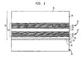
- FIG. 1is a fragmentary, diagrammatic sectional view on an enlarged scale of a semiconductor structure according to one embodiment of the present invention.
- FIG. 2is a comparative Nomarski image depicting a portion of a semiconductor structure in accordance with one embodiment of the present invention and another structure, not in accordance with the present invention, for comparison purposes.
- FIG. 3is a process flow diagram depicting a process in accordance with a further embodiment of the invention.
- FIG. 4is another process flow diagram depicting a process in accordance with yet another embodiment of the invention.
- FIG. 5is a view similar to that of FIG. 1 depicting a semiconductor structure according to a further embodiment of the invention.
- FIG. 6is a fragmentary, diagrammatic sectional view on an enlarged scale of a Schottky diode according to a still further embodiment of the invention.
- FIG. 7is a view similar to that of FIG. 6 depicting a Schottky diode according to an additional embodiment of the invention.
- III–V semiconductorrefers to a compound semiconductor material according to the stoichiometric formula Al a In b Ga c N d As e P f where (a+b+c) is about 1 and (d+e+f) is also about 1.
- nitride semiconductoror “nitride-based semiconductor” refers to a III–V semiconductor in which d is 0.5 or more, most typically about 0.8 or more. Most preferably, the semiconductor materials are pure nitride semiconductors, i.e., nitride semiconductors in which d is about 1.0.
- gallium nitride based semiconductorrefers to a nitride semiconductor including gallium, and most preferably including gallium as the principal metal present, i.e., having c ⁇ 0.5 and most preferably ⁇ 0.8.
- the semiconductorsmay have p-type or n-type conductivity, which may be imparted by conventional dopants and may also result from the inherent conductivity type of the particular semiconductor material. For example, gallium nitride-based semiconductors having defects typically are inherently n-type even when undoped.
- n-type nitride semiconductorsmay include conventional electron acceptor dopants such as Mg and Zn.
- a process according to one embodiment of the present inventionbegins with a doped silicon substrate 10 .
- the silicon substratemost preferably is a substantially mono-crystalline silicon wafer having a polished, flat top surface 12 .
- the top surfacedesirably is the (1,1,1) crystal plane of the silicon.
- the waferis brought to a temperature of about 600–900° C. in a conventional chemical vapor deposition apparatus and exposed to an organo-aluminum compound, most preferably a lower alkyl aluminum compound such as trimethyl aluminum (“TMA”) in vapor form for a few seconds.
- TMAtrimethyl aluminum
- FIG. 1is not drawn to scale.
- the thickness of aluminum layer 14is greatly exaggerated for clarity of illustration.
- the aluminum layerincludes only about 1–10 mono-layers of aluminum atoms and has a thickness less than about 100 ⁇ , more preferably less than about 50 ⁇ .
- the aluminum layeris depicted as a discrete, separate layer for clarity of illustration, it is believed that there is some diffusion of silicon into the aluminum layer 14 from substrate 10 , and also some diffusion of nitrogen into the aluminum layer from the overlying layers discussed below. Thus, it is believed that in the finished article the aluminum layer will take the form of either a thin aluminum-rich zone at the upper surface of wafer 10 .
- the aluminum layerserves to protect the silicon substrate from etching during exposure to ammonia in subsequent process steps, and accordingly the substrate, with the aluminum layer, is referred to herein as an “aluminum-protected” silicon substrate.
- the aluminum-protected substrateis exposed to a mixture of an organo-metallic compound, most preferably an organo-aluminum compound, and ammonia, together with a carrier gas, so as to deposit a thin layer 16 of a nitride semiconductor, most preferably AlN.
- the AlNis deposited at substrate temperature on the order of 600–900° C., i.e., a temperature low enough to promote deposition of the nitride semiconductor, such as AlN, in a substantially polycrystalline form resulting from nucleation of the nitride semiconductor at numerous sites on the substrate.
- Nucleation layer 16desirably is about 20–50 nm thick; here again, its thickness is greatly exaggerated in FIG. 1 for clarity of illustration.
- a first superlattice 18is deposited directly on the top of the nucleation layer.
- the “top” surface of a grown semiconductor structureshould be understood as the surface most remote from the substrate used in forming the structure, i.e., the surface facing upwardly in FIG. 1 .
- a statement that one structure is deposited “directly on” an other structureshould be understood as meaning that the one structure directly abuts the top surface of the other structure, without intervening layers.
- a statement that one structure is “over” an other structureshould be understood as meaning that the one structure is more remote from the substrate than the other structure, but does not exclude the presence of intervening layers.
- the first superlatticeincludes a plurality of layers 20 and 22 of nitride semiconductors having differing compositions.
- the layershave thicknesses on the order of 10 nm or less, typically 5 nm or less and most commonly 3 nm or less, so that the overall structure is more in the nature of a composite crystal lattice than a set of discrete, individual layers.
- each of layers 20 and 22is formed from a pure nitride semiconductor selected from the group consisting of gallium nitride, aluminum nitride and aluminum gallium nitride, i.e., the group of semiconductors defined by the stoichiometric formula Al R Ga (1-R) N, with the layers having unequal values of R. That is, layer 20 has the formula Al X Ga (1-X) N, whereas layer 22 has the formula Al Y Ga (1-Y) N, where X ⁇ Y.
- Superlattice 18as a whole, desirably includes about 5–15 repetitions of layers 20 and 22 , most preferably about 10 repetitions.
- layer 20may be pure AlN, whereas layer 22 may be Al 0.5 Ga 0.5 N.
- a pure AlN layeris deposited by exposing the substrate to an organo-aluminum compound ammonia and carrier gas as discussed above, whereas an AlGaN layer is deposited by exposing the substrate to a similar gas mixture also incorporating an organo-gallium compound, desirably a lower alkyl organogallium compound such as trimethylgallium.
- the thicknesses of the aluminum gallium nitride layers 22 and aluminum nitride layers 20desirably are substantially constant throughout the thickness of superlattice 18 . However, this is not essential.
- compositions and thicknesses of the layerscan be varied within the superlattice to provide compositional grading within the superlattice, i.e., so that the overall proportion of gallium and aluminum within the superlattice varies in the upward direction, away from substrate 10 .
- the individual layers in the superlatticemay include some indium in the metallic component.
- a thin intermediate layer 24 of a gallium nitride based semiconductoris deposited by exposing the substrate to a mixture of an organo-gallium compound, ammonia and a carrier gas, at a temperature of about 950 to about 1100° C.
- Layer 24most preferably is about 200 to about 400 nm thick.
- a second superlattice 26is formed over intermediate layer 24 , desirably directly on the intermediate layer.
- the second superlatticeis generally similar to the first superlattice 18 and incorporates alternating layers of an aluminum-rich nitride semiconductor such as AlN 28 and a gallium enriched nitride semiconductor such as Al 0.5 Ga 0.5 N. More generally, layers 28 have the stoiceometric formula Al P Ga (1-P) N and layers 30 have the stoiceometric formula Al Q Ga (1-Q) N, where P ⁇ Q.
- the thicknesses and layer compositions in the second superlatticemay be the same as or different from the thicknesses and layer compositions in the first superlattice.
- the period of the second superlattice 26may be less than that of the first superlattice.
- the second superlatticemay be superlattice composed of about 5–10 repetitions of layers 28 and 30 .
- the first superlattice 18 , intermediate layer 24 and second superlattice 26cooperatively constitute a buffer structure 32 .
- an operative structure 34is deposited over the buffer structure, and most preferably directly on the top surface of the second superlattice in the buffer structure.
- Operative structure 34includes one or more gallium nitride based semiconductors and may include other semiconductors as well. In its simplest form, operative structure 34 may include one a single relatively thick layer of a gallium nitride based semiconductor such as pure GaN.
- the operative structuremay include plural layers having differing compositions and/or dopings as used, for example, to make conventional devices such as optical electronic devices such as light-emitting diodes, laser diodes and the like, or electronic devices such as field effect transistors and Schottky diodes.
- the gallium nitride based semiconductors in the operative structuremay be deposited at conventional growth temperatures using MOCVD techniques.
- the resulting semiconductor structureincorporates a nitride structure 36 incorporating the nucleation layer 16 , buffer structure 32 and operative structure 34 .
- the nitride structurehas a top surface 38 remote from substrate 10 and a bottom surface 40 adjacent substrate 10 .
- the gallium nitride based semiconductors in the operative structurehave excellent crystal quality. After deposition, the structure can be cooled to room temperature and then removed from the reactor, without appreciable cracking of the gallium nitride based semiconductors in the operative structure.
- the present inventionis not limited by any theory of operation, it is believed that the combination of the compressive stress induced by the superlattices in the operative structure and in the intermediate layer 24 serves to suppress formation of defects and, moreover, placement of the first superlattice below the lowest gallium nitride layer in the structure (below intermediate layer 24 ) serves to further limit the formation of crystal defects.
- the aluminum layer 14serves to protect the silicon substrate from etching by the ammonia used to deposit the nitride semiconductors and, thus, serves to further limit formation of defects in the crystal. It is also believed that the compressive stress applied by the superlattices and, hence, by the buffer structure as a whole to the operative structure 34 serves to prevent cracking when the substrate and nitride structure are cooled to room temperature.
- the chambercan be purged of metals from the preceding layer by flushing it with a mixture of the hydrogen or nitrogen carrier gas and ammonia for a prolonged period.
- the quality of the structure depicted in FIG. 1is evidenced by the Nomarski images of FIG. 2 .
- the imaged marked (a)is a Nomarski image of a structure which is not in accordance with the present invention, formed by depositing gallium nitride directly on an aluminum nitride nucleation layer, whereas the structure marked (b) in FIG. 2 shows comparable structure with the buffer structure as discussed above with reference to FIG. 1 between the nucleation layer and the gallium nitride layer.
- Structure (a)shows numerous lines representing crystal defects due to surface cracking, whereas structure (b) is substantially free of such defects.
- the structure resulting from the process discussed above with reference to FIG. 1can be further processed using conventional techniques to form individual devices as, for example, by subdividing the nitride structure 36 and the silicon substrate 10 to form individual units, each incorporating a portion of the nitride structure and a corresponding portion of substrate 10 , and applying contacts to the resulting units and packaging the same.
- a semiconductor structure incorporating a silicon substrate 10 and a nitride structure 36which may be the same as or different from the nitride structure discussed above with reference to FIGS. 1 and 2 , is engaged with a temporary carrier 42 so that the top surface 38 of the nitride structure bears against the carrier, and the top surface of the nitride structure is bonded to the carrier, preferably by using a dielectric “glue” that promotes adhesion between the top nitride layer and the carrier.
- This dielectriccan be, for example, benzocyclobutene (BCB), methylsilsesquioxane (MSSQ), or a material such as those sold under the commercial designations FlareTM, SiLKTM, Parylene-N and PETI 5 .
- BCBbenzocyclobutene
- MSSQmethylsilsesquioxane
- FlareTMSiLKTM
- Parylene-NPETI 5
- the surfaces of, the nitride structure, the carrier, or both,is or are coated with the glue and then the surfaces are brought into contact under a relatively low temperature, below 400° C. If the subsequent processing steps do not need to go above 100° C., other polymers such as HMDS or photoresist can be used. Additionally, if solvents such as acetone are not in future processing steps, such soluble adhesives such as wax or CrystalbondTM may be used.
- Carrier 42is illustrated in FIG. 3 as a sapphire element, but the carrier can be formed from other materials which are inert to the other reagents used in the processes to follow and which can survive at the temperatures used in the process. Most preferably, the carrier also has a coefficient of thermal expansion close to that of the nitride structure, and also does not contaminate the nitride structure. Thus, the carrier desirably is substantially free of materials which tend to diffuse into the nitride structure.
- the substrate 10is removed as by etching it away from the nitride structure 36 , preferably by using an etchant such as a potassium hydroxide solution as, for example, 20% KOH by weight aqueous solution at 70° C., which attacks the silicon substrate but which does not appreciably attach the nitride structure.
- an etchantsuch as a potassium hydroxide solution as, for example, 20% KOH by weight aqueous solution at 70° C.
- the nitride structureacts as a “etch stop”; the etching continues until the nitride structure is reached.
- An additional etch stopmay be provided at or adjacent the nitride structure. For example, a layer of SiO 2 will effectively stop etching by KOH.
- the bottom surface 40 of the nitride structureis exposed.
- a base 44is applied onto bottom surface 40 , as by chemical vapor deposition or sputtering of a base material on the bottom surface.
- the base materialdesirably is a material having good electrical insulating properties such as aluminum nitride or a carbonaceous, diamond-like material.
- Base material 44desirably also has relatively high thermal conductivity.
- Base material 44may be grown on the exposed bottom surface of the nitride structure, even if there is a substantial crystal lattice mismatch between the nitride structure and the base material.
- the base materialneed not form as a mono-crystalline, defect-free structure, provided that the poly-crystalline or defect-laden base material retains the desired insulating properties.
- aluminum nitride or carboncan be deposited by chemical vapor deposition.
- a tape or other temporary handling element 46is applied onto the exposed surface of base 44 and the carrier 42 is removed, leaving the nitride structure 36 on base 44 and physically supported by the base and by the tape or other temporary handling element 46 , and leaving the nitride structure with its bottom surface 40 confronting the base 44 .
- the resulting structureis devoid of the silicon substrate used during epitaxial growth of the nitride structure.
- the resulting structurecan be subjected to conventional semiconductor processing techniques such as subdividing, application of contacts and mounting to a package to form one or more usable devices.
- the base material deposition stepcan be omitted.
- a nitride structure on a silicon growth substrate 110is subjected to post-growth processing as, for example, application of contacts, subdivision and etching so as to form a plurality of semi-finished gallium nitride devices 136 on the silicon growth substrate 110 , each such semi-finished device incorporating a gallium nitride structure.
- the semi-finished devicesare subjected to process steps similar to those discussed above with reference to FIG. 3 , including application of a temporary carrier 142 overlying the top surfaces of the gallium nitride structures and removal of the substrate to expose the bottom surfaces 140 of these structures.
- a base materialis applied so as to form a base 144 on each gallium nitride structure 140 .
- a temporary handling elementsuch as a tape 146 may be applied and the devices may be subjected to procedures such as lead-bonding and mounting on a package element 148 .
- the finished devices prepared according to the methods discussed above with reference to FIGS. 3 and 4can provide superior electrical properties because the silicon substrate used in epitaxial growth of the nitride structure is not present in the finished device. Although relatively expensive materials as, for example, sapphire wafers are employed as temporary carriers, these can be recycled and reused, and form no part of the finished device.
- the aluminum layer and aluminum-protected silicon substrate discussed abovecan be utilized in growth of other nitride semiconductor structures and other III–V semiconductor structures.
- the III–V semiconductors used in the preferred embodimentscan be varied by addition of other group V elements as, for example, As and P.
- the buffer structure incorporated in the nitride structuremay include more than two superlattices.
- the intermediate layer and second superlatticecan be omitted. In one such variant, depicted in FIG.
- the second superlatticeis omitted and replaced by a further polycrystalline nucleation layer as, for example, a layer of AlN deposited at a low temperature.
- This structureincludes a substrate 210 and aluminum layer 214 identical to the corresponding structures discussed above with reference to FIG. 1 .
- the nucleation layer 214consists of 30 nm thick AlN.
- the buffer structure 232includes a first superlattice 218 having 10 repetitions of a basic unit, each unit including a layer 220 of AlN 2 nm thick and a layer 222 of Al 0.3 Ga 0.7 N, also 2 nm thick.
- the buffer structure 232further includes an intermediate layer 224 of GaN 0.4 ⁇ m thick, and a nucleation layer 226 of 13 nm thick polycrystalline AlN.
- the operative structure 235includes a layer 235 of GaN 0.6 ⁇ m thick and a top layer 237 of Al 0.3 Ga 0.7 N 23 nm thick. Layers 237 and 235 cooperatively provide a two-dimensional electron gas and contribute to operation of the device as a high electron mobility transistor.
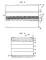
- FIG. 6illustrates a cross-sectional view of a nitride semiconductor Schottky diode 300 formed in accordance with a further embodiment of the invention.
- the Schottky diode 300includes a doped silicon substrate 302 upon which is formed a buffer structure 304 which may be the buffer structure 32 shown in FIG. 1 or the buffer structure 232 shown in FIG. 5 .
- the buffer structuretypically has a thickness of between 0.1 to 10 microns.
- a highly doped n-type nitride semiconductor layer 306such as a layer of GaN or other gallium nitride-based semiconductor, is formed atop the buffer structure 302 and has a doping concentration of between 10 18 to 10 19 cm ⁇ 3 with a thickness of between 0.1 to 10 microns.
- a lower doped n-type nitride semiconductor layer 308is formed atop the highly doped nitride semiconductor layer and may also be comprised of GaN or another gallium nitride-based semiconductor. The concentration of dopants in the lower doped layer is between 10 15 to 10 16 cm ⁇ 3 , and the layer has a thickness of between 0.1 to 10 microns.
- the more highly doped layer 306is omitted, and the lower doped layer 308 is formed directly atop the buffer structure 304 .
- a Schottky contact layer 310is deposited atop the lower doped layer 308 and preferably covers the complete width of the lower doped layer.
- a thick metal layer 312is disposed atop the Schottky contact layer 310 .
- a thin ohmic metal contact layer 316is formed on the backside of the silicon substrate 302 , and another metal stack 318 is deposited atop the ohmic metal layer 316 .
- An optional passivation layer 314may be formed atop all of or part of the Schottky contact metal layer 310 and the thick metal layer 312 .
- the structure of the Schottky diode 300provides a forward direction, vertical current conduction path from the Schottky contact metal and through the low doped layer 308 , the highly doped layer 306 , the buffer structure 304 and the silicon substrate 302 to the ohmic metal layer 316 and metal stack 318 . Additionally, the width of the Schottky contact metal layer 310 and the metal stack 312 provide a vertical conduction path that utilizes the full width of the Schottky diode structure.
- the vertical conduction pathminimizes the resistance of the device while under forward bias but maintains a high breakdown voltage while under reverse bias.
- the turn-on voltage of the deviceis typically between 0.5V and 1.5V while the breakdown voltage is greater than ⁇ 100V.
- the on-resistance of the deviceis less than 10–20 milliohm-cm 2 , whereas known devices in the industry typically have resistances greater than this value.
- the vertical conduction path of the Schottky diodeis particularly useful in achieving a low on-resistance in a gallium nitride based diode even though the GaN and other nitride-based semiconductors used typically have relatively high resistances.
- Known GaN-based semiconductor devices grown on an insulating substrate, such as sapphiretypically use lateral conduction in the nitride-based layers to carry the forward current. The forward current must travel over a relatively long path as well as along relatively thin layers of highly resistive material that have small cross-sectional areas in the direction transverse to the direction of current flow.
- the path lengthis determined by the horizontal dimensions of the die (e.g., a millimeter or more) and the cross-sectional area is determined by the thickness of the GaN layers (e.g., a few microns).
- the path length between the silicon substrate and the Schottky contacthas a miniscule length, equal to the thickness of the GaN layers (a few microns), and has a substantial cross-sectional area, corresponding to the surface area of the die structure, thereby substantially reducing the resistance of the device.
- the reduction in on-resistance due to the vertical conducting structureis achieved using a relatively inexpensive, highly conductive silicon substrate.
- this low on-resistancecan be achieved while maintaining high crystal quality in the nitride-based semiconductors.
- the doping levels in the nitride-based semiconductorscan be relatively low, which aids in maintaining a high breakdown voltage, without incurring excessive on-resistance.
- FIG. 7illustrates another embodiment of a vertical conduction Schottky diode 400 formed in accordance with the invention but having a mesa structure.
- a buffer structure 404is formed on the top surface of a silicon substrate 402 in accordance with one of the methods descried above with a structure corresponding to one of the above-described structures.
- a highly doped, n-type nitride semiconductor layer 406is disposed atop the buffer structure 404 and has a composition, doping concentration and thickness similar to the corresponding region of the device shown in FIG. 6 .
- a lower doped, n-type nitride semiconductor layer 408is formed atop the highly doped layer 406 and likewise has a composition, doping concentration and thickness similar to the corresponding region shown in FIG.
- the width of the lower doped layer 408is less than the width of the more highly doped layer.
- the Schottky contact metal layer 410 and the upper thick metal stack 412are similar in structure and thickness to the corresponding layers shown in FIG. 6 but have a width similar to the lower doped layer 408 .
- An edge termination structure(not shown) may be formed to counter any edge effects resulting from the Schottky contact metal.
- a passivation layermay also be included.
- An ohmic contact metal layer 416 and a metal stack 418are formed on the backside of the silicon substrate.
Landscapes
- Engineering & Computer Science (AREA)
- Microelectronics & Electronic Packaging (AREA)
- Condensed Matter Physics & Semiconductors (AREA)
- General Physics & Mathematics (AREA)
- Manufacturing & Machinery (AREA)
- Computer Hardware Design (AREA)
- Physics & Mathematics (AREA)
- Power Engineering (AREA)
- Chemical & Material Sciences (AREA)
- Materials Engineering (AREA)
- Crystallography & Structural Chemistry (AREA)
- Metallurgy (AREA)
- Organic Chemistry (AREA)
- Recrystallisation Techniques (AREA)
- Junction Field-Effect Transistors (AREA)
Abstract
Description
Claims (31)
Priority Applications (2)
| Application Number | Priority Date | Filing Date | Title |
|---|---|---|---|
| US10/721,488US7115896B2 (en) | 2002-12-04 | 2003-11-25 | Semiconductor structures for gallium nitride-based devices |
| US11/371,738US20060154455A1 (en) | 2002-12-04 | 2006-03-09 | Gallium nitride-based devices and manufacturing process |
Applications Claiming Priority (2)
| Application Number | Priority Date | Filing Date | Title |
|---|---|---|---|
| US43083702P | 2002-12-04 | 2002-12-04 | |
| US10/721,488US7115896B2 (en) | 2002-12-04 | 2003-11-25 | Semiconductor structures for gallium nitride-based devices |
Related Child Applications (1)
| Application Number | Title | Priority Date | Filing Date |
|---|---|---|---|
| US11/371,738DivisionUS20060154455A1 (en) | 2002-12-04 | 2006-03-09 | Gallium nitride-based devices and manufacturing process |
Publications (2)
| Publication Number | Publication Date |
|---|---|
| US20040119063A1 US20040119063A1 (en) | 2004-06-24 |
| US7115896B2true US7115896B2 (en) | 2006-10-03 |
Family
ID=32469541
Family Applications (2)
| Application Number | Title | Priority Date | Filing Date |
|---|---|---|---|
| US10/721,488Expired - LifetimeUS7115896B2 (en) | 2002-12-04 | 2003-11-25 | Semiconductor structures for gallium nitride-based devices |
| US11/371,738AbandonedUS20060154455A1 (en) | 2002-12-04 | 2006-03-09 | Gallium nitride-based devices and manufacturing process |
Family Applications After (1)
| Application Number | Title | Priority Date | Filing Date |
|---|---|---|---|
| US11/371,738AbandonedUS20060154455A1 (en) | 2002-12-04 | 2006-03-09 | Gallium nitride-based devices and manufacturing process |
Country Status (9)
| Country | Link |
|---|---|
| US (2) | US7115896B2 (en) |
| EP (1) | EP1568083A4 (en) |
| JP (1) | JP4095066B2 (en) |
| KR (1) | KR100773997B1 (en) |
| CN (1) | CN1692499A (en) |
| AU (1) | AU2003298891A1 (en) |
| DE (1) | DE10392313B4 (en) |
| TW (1) | TWI249246B (en) |
| WO (1) | WO2004051707A2 (en) |
Cited By (28)
| Publication number | Priority date | Publication date | Assignee | Title |
|---|---|---|---|---|
| US20060145283A1 (en)* | 2005-01-06 | 2006-07-06 | Zhu Tinggang | Gallium nitride semiconductor device |
| US20060175681A1 (en)* | 2005-02-08 | 2006-08-10 | Jing Li | Method to grow III-nitride materials using no buffer layer |
| US20080054248A1 (en)* | 2006-09-06 | 2008-03-06 | Chua Christopher L | Variable period variable composition supperlattice and devices including same |
| US20090149008A1 (en)* | 2007-10-05 | 2009-06-11 | Applied Materials, Inc. | Method for depositing group iii/v compounds |
| US20100032718A1 (en)* | 2008-08-11 | 2010-02-11 | Chia-Lin Yu | III-Nitride Based Semiconductor Structure with Multiple Conductive Tunneling Layer |
| US20100215854A1 (en)* | 2007-06-24 | 2010-08-26 | Burrows Brian H | Hvpe showerhead design |
| US20100261340A1 (en)* | 2009-04-10 | 2010-10-14 | Applied Materials, Inc. | Cluster tool for leds |
| US20100273290A1 (en)* | 2009-04-28 | 2010-10-28 | Applied Materials, Inc. | Mocvd single chamber split process for led manufacturing |
| US20100273318A1 (en)* | 2009-04-24 | 2010-10-28 | Applied Materials, Inc. | Substrate pretreatment for subsequent high temperature group iii depositions |
| US20100279020A1 (en)* | 2009-04-29 | 2010-11-04 | Applied Materials, Inc. | METHOD OF FORMING IN-SITU PRE-GaN DEPOSITION LAYER IN HVPE |
| US20110215339A1 (en)* | 2007-03-20 | 2011-09-08 | Power Integrations, Inc. | Termination and contact structures for a high voltage GaN-based heterojunction transistor |
| US8361892B2 (en) | 2010-04-14 | 2013-01-29 | Applied Materials, Inc. | Multiple precursor showerhead with by-pass ports |
| US8491720B2 (en) | 2009-04-10 | 2013-07-23 | Applied Materials, Inc. | HVPE precursor source hardware |
| US8497146B2 (en) | 2011-08-25 | 2013-07-30 | Micron Technology, Inc. | Vertical solid-state transducers having backside terminals and associated systems and methods |
| US8513643B2 (en) | 2006-09-06 | 2013-08-20 | Palo Alto Research Center Incorporated | Mixed alloy defect redirection region and devices including same |
| US8629525B2 (en) | 2005-11-15 | 2014-01-14 | Power Integrations, Inc. | Second contact schottky metal layer to improve GaN schottky diode performance |
| US8633094B2 (en) | 2011-12-01 | 2014-01-21 | Power Integrations, Inc. | GaN high voltage HFET with passivation plus gate dielectric multilayer structure |
| US20140061663A1 (en)* | 2012-09-04 | 2014-03-06 | Samsung Electronics Co., Ltd | Semiconductor buffer structure, semiconductor device including the same, and manufacturing method thereof |
| US20140252366A1 (en)* | 2013-03-06 | 2014-09-11 | Iqe Rf, Llc | Semiconductor Structure Including Buffer With Strain Compensation Layers |
| US8916929B2 (en) | 2004-06-10 | 2014-12-23 | Power Integrations, Inc. | MOSFET having a JFET embedded as a body diode |
| US8928037B2 (en) | 2013-02-28 | 2015-01-06 | Power Integrations, Inc. | Heterostructure power transistor with AlSiN passivation layer |
| US8940620B2 (en) | 2011-12-15 | 2015-01-27 | Power Integrations, Inc. | Composite wafer for fabrication of semiconductor devices |
| US8946773B2 (en) | 2012-08-09 | 2015-02-03 | Samsung Electronics Co., Ltd. | Multi-layer semiconductor buffer structure, semiconductor device and method of manufacturing the semiconductor device using the multi-layer semiconductor buffer structure |
| US8952395B2 (en)* | 2011-07-26 | 2015-02-10 | Micron Technology, Inc. | Wafer-level solid state transducer packaging transducers including separators and associated systems and methods |
| US9057128B2 (en) | 2011-03-18 | 2015-06-16 | Applied Materials, Inc. | Multiple level showerhead design |
| US9691940B2 (en) | 2015-05-06 | 2017-06-27 | Episil-Precision Inc. | Nitride semiconductor structure |
| US11869942B2 (en)* | 2017-08-28 | 2024-01-09 | Siltronic Ag | Heteroepitaxial wafer and method for producing a heteroepitaxial wafer |
| US12125938B2 (en) | 2006-02-23 | 2024-10-22 | Azur Space Solar Power Gmbh | Nitride semiconductor component and process for its production |
Families Citing this family (112)
| Publication number | Priority date | Publication date | Assignee | Title |
|---|---|---|---|---|
| CN1034730C (en)* | 1992-09-29 | 1997-04-30 | 南京师范大学 | Method of dunaliella collecting and beta-carotene extracting |
| JPH07231959A (en)* | 1994-02-23 | 1995-09-05 | Torai Toentei One Kk | Golfbag with stand |
| US7601441B2 (en)* | 2002-06-24 | 2009-10-13 | Cree, Inc. | One hundred millimeter high purity semi-insulating single crystal silicon carbide wafer |
| US6814801B2 (en)* | 2002-06-24 | 2004-11-09 | Cree, Inc. | Method for producing semi-insulating resistivity in high purity silicon carbide crystals |
| US20070063185A1 (en)* | 2003-06-26 | 2007-03-22 | Rj Mears, Llc | Semiconductor device including a front side strained superlattice layer and a back side stress layer |
| US20070063186A1 (en)* | 2003-06-26 | 2007-03-22 | Rj Mears, Llc | Method for making a semiconductor device including a front side strained superlattice layer and a back side stress layer |
| TWI252599B (en)* | 2004-04-27 | 2006-04-01 | Showa Denko Kk | N-type group III nitride semiconductor layered structure |
| KR100670531B1 (en) | 2004-08-26 | 2007-01-16 | 엘지이노텍 주식회사 | Nitride semiconductor light emitting device and manufacturing method |
| EP1794813B1 (en)* | 2004-08-26 | 2015-05-20 | LG Innotek Co., Ltd. | Nitride semiconductor light emitting device and fabrication method thereof |
| FR2875337A1 (en)* | 2004-09-13 | 2006-03-17 | Picogiga Internat Soc Par Acti | PIEZOELECTRIC HEMT STRUCTURES WITH NO ZERO ALLOYS |
| FR2875338B1 (en)* | 2004-09-13 | 2007-01-05 | Picogiga Internat Soc Par Acti | METHOD FOR PRODUCING PIEZOELECTRIC HEMT STRUCTURES WITH NO ZERO ALLOYS |
| CN100356595C (en)* | 2004-09-27 | 2007-12-19 | 晶元光电股份有限公司 | Group III nitride semiconductor device and manufacturing method thereof |
| JP4826703B2 (en)* | 2004-09-29 | 2011-11-30 | サンケン電気株式会社 | Plate-like substrate for use in forming semiconductor elements |
| US7247889B2 (en) | 2004-12-03 | 2007-07-24 | Nitronex Corporation | III-nitride material structures including silicon substrates |
| DE102005010821B4 (en)* | 2005-03-07 | 2007-01-25 | Technische Universität Berlin | Method for producing a component |
| JP4563230B2 (en)* | 2005-03-28 | 2010-10-13 | 昭和電工株式会社 | Method for manufacturing AlGaN substrate |
| WO2006113539A2 (en)* | 2005-04-13 | 2006-10-26 | Group4 Labs, Llc | Semiconductor devices having gallium nitride epilayers on diamond substrates |
| US8674405B1 (en)* | 2005-04-13 | 2014-03-18 | Element Six Technologies Us Corporation | Gallium—nitride-on-diamond wafers and devices, and methods of manufacture |
| US9157169B2 (en)* | 2005-09-14 | 2015-10-13 | International Rectifier Corporation | Process for manufacture of super lattice using alternating high and low temperature layers to block parasitic current path |
| KR100661602B1 (en)* | 2005-12-09 | 2006-12-26 | 삼성전기주식회사 | Method of manufacturing vertical structure gallium nitride based LED device |
| KR20070062686A (en)* | 2005-12-13 | 2007-06-18 | 엘지이노텍 주식회사 | Nitride semiconductor light emitting device and manufacturing method |
| JP4897285B2 (en)* | 2005-12-14 | 2012-03-14 | 国立大学法人徳島大学 | Substrate for semiconductor device and method for manufacturing the same |
| EP1842940A1 (en)* | 2006-04-06 | 2007-10-10 | Interuniversitair Microelektronica Centrum ( Imec) | Method for forming a group III nitride material on a silicon substrate |
| KR100691635B1 (en)* | 2006-06-13 | 2007-03-12 | 삼성전기주식회사 | A substrate for growing a group III nitride semiconductor, a method of manufacturing a vertical structure LED device and a substrate for growing a group III nitride semiconductor using the same |
| JP5309451B2 (en)* | 2007-02-19 | 2013-10-09 | サンケン電気株式会社 | Semiconductor wafer, semiconductor device, and manufacturing method |
| JP5309452B2 (en)* | 2007-02-28 | 2013-10-09 | サンケン電気株式会社 | Semiconductor wafer, semiconductor device, and manufacturing method |
| DE102008030584A1 (en) | 2008-06-27 | 2009-12-31 | Osram Opto Semiconductors Gmbh | Method for producing an optoelectronic component and optoelectronic component |
| GB2467911B (en)* | 2009-02-16 | 2013-06-05 | Rfmd Uk Ltd | A semiconductor structure and a method of manufacture thereof |
| JP5133927B2 (en)* | 2009-03-26 | 2013-01-30 | コバレントマテリアル株式会社 | Compound semiconductor substrate |
| JP2010263189A (en)* | 2009-04-07 | 2010-11-18 | Sharp Corp | Nitride semiconductor light emitting diode |
| US20110017972A1 (en) | 2009-07-22 | 2011-01-27 | Rfmd (Uk) Limited | Light emitting structure with integral reverse voltage protection |
| KR101358633B1 (en)* | 2009-11-04 | 2014-02-04 | 도와 일렉트로닉스 가부시키가이샤 | Epitaxially laminated iii-nitride substrate |
| KR101105918B1 (en)* | 2009-11-30 | 2012-01-17 | 주식회사 엘지실트론 | Manufacturing Method of Nitride Semiconductor Device |
| US8785305B2 (en)* | 2009-12-11 | 2014-07-22 | National Semiconductor Corporation | Backside stress compensation for gallium nitride or other nitride-based semiconductor devices |
| WO2011102045A1 (en)* | 2010-02-16 | 2011-08-25 | 日本碍子株式会社 | Epitaxial substrate and method for producing same |
| WO2011122322A1 (en)* | 2010-03-31 | 2011-10-06 | 日本碍子株式会社 | Epitaxial substrate and method of manufacturing epitaxial substrate |
| JP5689245B2 (en) | 2010-04-08 | 2015-03-25 | パナソニック株式会社 | Nitride semiconductor device |
| WO2011135963A1 (en)* | 2010-04-28 | 2011-11-03 | 日本碍子株式会社 | Epitaxial substrate and process for producing epitaxial substrate |
| JP5596783B2 (en)* | 2010-04-28 | 2014-09-24 | 日本碍子株式会社 | Epitaxial substrate and epitaxial substrate manufacturing method |
| EP2581929A4 (en)* | 2010-06-08 | 2014-04-02 | Ngk Insulators Ltd | EPITAXIAL SUBSTRATE, AND METHOD FOR PRODUCING EPITAXIAL SUBSTRATE |
| JP5614130B2 (en)* | 2010-06-30 | 2014-10-29 | 住友電気工業株式会社 | Manufacturing method of semiconductor device |
| KR101692410B1 (en)* | 2010-07-26 | 2017-01-03 | 삼성전자 주식회사 | Light emitting device and method of manufacturing the same |
| JP5660373B2 (en)* | 2010-10-29 | 2015-01-28 | サンケン電気株式会社 | Semiconductor wafer and semiconductor device |
| JP5707903B2 (en)* | 2010-12-02 | 2015-04-30 | 富士通株式会社 | Compound semiconductor device and manufacturing method thereof |
| US20120149176A1 (en)* | 2010-12-10 | 2012-06-14 | Taiwan Semiconductor Manufacturing Company, Ltd. | Method and apparatus for forming a iii-v family layer |
| US8400219B2 (en) | 2011-03-24 | 2013-03-19 | Suvolta, Inc. | Analog circuits having improved transistors, and methods therefor |
| JP5911727B2 (en)* | 2011-05-16 | 2016-04-27 | 株式会社東芝 | Nitride semiconductor element, nitride semiconductor wafer, and method of manufacturing nitride semiconductor layer |
| KR101855063B1 (en)* | 2011-06-24 | 2018-05-04 | 엘지이노텍 주식회사 | Light emitting device |
| KR20130014861A (en)* | 2011-08-01 | 2013-02-12 | 삼성전자주식회사 | High electron mobility transistor and method of manufacturing the same |
| KR101853640B1 (en)* | 2011-08-24 | 2018-06-20 | 엘지이노텍 주식회사 | Semiconductor device |
| JP5903818B2 (en)* | 2011-09-26 | 2016-04-13 | 富士通株式会社 | Compound semiconductor device and manufacturing method thereof |
| CN105633234A (en)* | 2012-03-15 | 2016-06-01 | 安徽三安光电有限公司 | Gallium nitride-based semiconductor growth substrate and fabrication method thereof |
| JP6100047B2 (en)* | 2012-03-26 | 2017-03-22 | 株式会社アルバック | Method for forming gallium nitride film and apparatus for forming gallium nitride film |
| US9093420B2 (en) | 2012-04-18 | 2015-07-28 | Rf Micro Devices, Inc. | Methods for fabricating high voltage field effect transistor finger terminations |
| CN102664188B (en)* | 2012-05-10 | 2014-07-23 | 电子科技大学 | Gallium nitride-based high-electron-mobility transistor with composite buffering layer |
| KR20130137773A (en)* | 2012-06-08 | 2013-12-18 | 엘지이노텍 주식회사 | Semiconductor device |
| KR20130139707A (en)* | 2012-06-13 | 2013-12-23 | 삼성전자주식회사 | Semiconductor device and superlattice layer used therefor |
| US9124221B2 (en) | 2012-07-16 | 2015-09-01 | Rf Micro Devices, Inc. | Wide bandwidth radio frequency amplier having dual gate transistors |
| US8988097B2 (en) | 2012-08-24 | 2015-03-24 | Rf Micro Devices, Inc. | Method for on-wafer high voltage testing of semiconductor devices |
| US9917080B2 (en) | 2012-08-24 | 2018-03-13 | Qorvo US. Inc. | Semiconductor device with electrical overstress (EOS) protection |
| US9202874B2 (en) | 2012-08-24 | 2015-12-01 | Rf Micro Devices, Inc. | Gallium nitride (GaN) device with leakage current-based over-voltage protection |
| US9147632B2 (en) | 2012-08-24 | 2015-09-29 | Rf Micro Devices, Inc. | Semiconductor device having improved heat dissipation |
| US9142620B2 (en) | 2012-08-24 | 2015-09-22 | Rf Micro Devices, Inc. | Power device packaging having backmetals couple the plurality of bond pads to the die backside |
| US9070761B2 (en) | 2012-08-27 | 2015-06-30 | Rf Micro Devices, Inc. | Field effect transistor (FET) having fingers with rippled edges |
| US9129802B2 (en) | 2012-08-27 | 2015-09-08 | Rf Micro Devices, Inc. | Lateral semiconductor device with vertical breakdown region |
| JP6120204B2 (en)* | 2012-09-06 | 2017-04-26 | パナソニック株式会社 | Epitaxial wafer, manufacturing method thereof, and ultraviolet light emitting device |
| JP6090899B2 (en)* | 2012-09-06 | 2017-03-08 | パナソニック株式会社 | Epitaxial wafer manufacturing method |
| US9583574B2 (en)* | 2012-09-28 | 2017-02-28 | Intel Corporation | Epitaxial buffer layers for group III-N transistors on silicon substrates |
| US9325281B2 (en) | 2012-10-30 | 2016-04-26 | Rf Micro Devices, Inc. | Power amplifier controller |
| KR20140133085A (en)* | 2013-05-09 | 2014-11-19 | 엘지이노텍 주식회사 | Semiconductor device and method for manufacturing the device |
| DE112014003533T5 (en)* | 2013-07-30 | 2016-04-14 | Sumitomo Chemical Company, Limited | Semiconductor wafer and method for producing the semiconductor wafer |
| CN105612622B (en)* | 2013-09-27 | 2019-02-22 | 英特尔公司 | Forming LED structures on silicon fins |
| KR102137743B1 (en)* | 2013-10-07 | 2020-07-24 | 엘지이노텍 주식회사 | Semiconductor device |
| KR102098250B1 (en) | 2013-10-21 | 2020-04-08 | 삼성전자 주식회사 | Semiconductor buffer structure, semiconductor device employing the same and method of manufacturing semiconductor device using the semiconductor buffer structure |
| KR102182016B1 (en)* | 2013-12-02 | 2020-11-23 | 엘지이노텍 주식회사 | Semiconductor device and semiconductor circuit including the device |
| US9455327B2 (en) | 2014-06-06 | 2016-09-27 | Qorvo Us, Inc. | Schottky gated transistor with interfacial layer |
| US9536803B2 (en) | 2014-09-05 | 2017-01-03 | Qorvo Us, Inc. | Integrated power module with improved isolation and thermal conductivity |
| FR3028670B1 (en)* | 2014-11-18 | 2017-12-22 | Commissariat Energie Atomique | SEMICONDUCTOR SEMICONDUCTOR LAYER STRUCTURE OF GROUP III-V OR II-VI COMPRISING CRYSTALLINE STRUCTURE WITH CUBIC OR HEXAGONAL MESH |
| CN104393130B (en)* | 2014-12-15 | 2017-04-12 | 聚灿光电科技股份有限公司 | GaN-based LED (Light-emitting Diode) epitaxy structure and preparation method thereof |
| US10062684B2 (en) | 2015-02-04 | 2018-08-28 | Qorvo Us, Inc. | Transition frequency multiplier semiconductor device |
| US10615158B2 (en) | 2015-02-04 | 2020-04-07 | Qorvo Us, Inc. | Transition frequency multiplier semiconductor device |
| US10109736B2 (en)* | 2015-02-12 | 2018-10-23 | Taiwan Semiconductor Manufacturing Co., Ltd. | Superlattice buffer structure for gallium nitride transistors |
| KR102355604B1 (en)* | 2015-07-03 | 2022-01-26 | 쑤저우 레킨 세미컨덕터 컴퍼니 리미티드 | Light emitting device and light unit having thereof |
| US11289593B2 (en)* | 2015-07-31 | 2022-03-29 | Infineon Technologies Austria Ag | Breakdown resistant HEMT substrate and device |
| US9773898B2 (en) | 2015-09-08 | 2017-09-26 | Macom Technology Solutions Holdings, Inc. | III-nitride semiconductor structures comprising spatially patterned implanted species |
| US9799520B2 (en) | 2015-09-08 | 2017-10-24 | Macom Technology Solutions Holdings, Inc. | Parasitic channel mitigation via back side implantation |
| US9806182B2 (en) | 2015-09-08 | 2017-10-31 | Macom Technology Solutions Holdings, Inc. | Parasitic channel mitigation using elemental diboride diffusion barrier regions |
| US20170069721A1 (en) | 2015-09-08 | 2017-03-09 | M/A-Com Technology Solutions Holdings, Inc. | Parasitic channel mitigation using silicon carbide diffusion barrier regions |
| US9627473B2 (en) | 2015-09-08 | 2017-04-18 | Macom Technology Solutions Holdings, Inc. | Parasitic channel mitigation in III-nitride material semiconductor structures |
| US9704705B2 (en) | 2015-09-08 | 2017-07-11 | Macom Technology Solutions Holdings, Inc. | Parasitic channel mitigation via reaction with active species |
| US9673281B2 (en) | 2015-09-08 | 2017-06-06 | Macom Technology Solutions Holdings, Inc. | Parasitic channel mitigation using rare-earth oxide and/or rare-earth nitride diffusion barrier regions |
| US10211294B2 (en) | 2015-09-08 | 2019-02-19 | Macom Technology Solutions Holdings, Inc. | III-nitride semiconductor structures comprising low atomic mass species |
| FR3041470B1 (en)* | 2015-09-17 | 2017-11-17 | Commissariat Energie Atomique | SEMICONDUCTOR STRUCTURE HAVING IMPROVED TENSION |
| US9806183B2 (en)* | 2015-11-30 | 2017-10-31 | Veeco Instruments, Inc. | Stress control on thin silicon substrates |
| JP7003058B2 (en)* | 2016-04-15 | 2022-02-04 | スージョウ レキン セミコンダクター カンパニー リミテッド | Light emitting element, light emitting element package and light emitting module |
| SG11201901373YA (en)* | 2016-08-23 | 2019-03-28 | Qromis Inc | Electronic power devices integrated with an engineered substrate |
| US9917156B1 (en) | 2016-09-02 | 2018-03-13 | IQE, plc | Nucleation layer for growth of III-nitride structures |
| US10720520B2 (en) | 2017-06-21 | 2020-07-21 | Infineon Technologies Austria Ag | Method of controlling wafer bow in a type III-V semiconductor device |
| JP6512669B2 (en)* | 2017-10-19 | 2019-05-15 | 国立大学法人 名古屋工業大学 | Semiconductor laminated structure and semiconductor device using the same |
| EP3503163A1 (en) | 2017-12-21 | 2019-06-26 | EpiGan NV | A method for forming a silicon carbide film onto a silicon substrate |
| US10516076B2 (en)* | 2018-02-01 | 2019-12-24 | Silanna UV Technologies Pte Ltd | Dislocation filter for semiconductor devices |
| US11038023B2 (en) | 2018-07-19 | 2021-06-15 | Macom Technology Solutions Holdings, Inc. | III-nitride material semiconductor structures on conductive silicon substrates |
| CN112687732B (en) | 2019-10-17 | 2024-02-02 | 三星电子株式会社 | Semiconductor thin film structure and electronic device including the same |
| CN112750904B (en) | 2019-10-30 | 2024-01-02 | 联华电子股份有限公司 | Semiconductor element with stress relaxation layer |
| US11749758B1 (en) | 2019-11-05 | 2023-09-05 | Semiq Incorporated | Silicon carbide junction barrier schottky diode with wave-shaped regions |
| US11469333B1 (en) | 2020-02-19 | 2022-10-11 | Semiq Incorporated | Counter-doped silicon carbide Schottky barrier diode |
| WO2022068256A1 (en)* | 2020-09-30 | 2022-04-07 | 苏州能讯高能半导体有限公司 | Epitaxial structure of semiconductor device and preparation method therefor |
| CN113658853B (en)* | 2021-08-16 | 2024-07-02 | 上海新微半导体有限公司 | Manufacturing method of GaN heteroepitaxial buffer layer based on Al ion implantation |
| US12217960B2 (en)* | 2021-08-31 | 2025-02-04 | Taiwan Semiconductor Manufacturing Co., Ltd. | Semiconductor devices and methods of manufacture |
| CN114883405B (en)* | 2022-05-30 | 2025-09-19 | 湖南三安半导体有限责任公司 | Semiconductor epitaxial structure, semiconductor device and preparation method thereof |
| CN117293174A (en)* | 2022-06-16 | 2023-12-26 | 华为技术有限公司 | Radio frequency semiconductor device, electronic equipment and preparation method of radio frequency semiconductor device |
| EP4614548A1 (en)* | 2024-03-08 | 2025-09-10 | Epinovatech AB | A semiconductor structure with strained bottom layer |
Citations (21)
| Publication number | Priority date | Publication date | Assignee | Title |
|---|---|---|---|---|
| EP0380340A2 (en) | 1989-01-25 | 1990-08-01 | Cree Research, Inc. | Silicon carbide Schottky diode and method of making same |
| DE4210402A1 (en) | 1991-03-29 | 1992-10-01 | Kobe Steel Ltd | DIAMOND SCHOTTKY DIODE |
| US5158909A (en) | 1987-12-04 | 1992-10-27 | Sanken Electric Co., Ltd. | Method of fabricating a high voltage, high speed Schottky semiconductor device |
| US5602418A (en) | 1992-08-07 | 1997-02-11 | Asahi Kasei Kogyo Kabushiki Kaisha | Nitride based semiconductor device and manufacture thereof |
| US5622877A (en) | 1993-03-02 | 1997-04-22 | Ramot University Authority For Applied Research & Industrial Development Ltd. | Method for making high-voltage high-speed gallium arsenide power Schottky diode |
| US5877558A (en) | 1993-04-28 | 1999-03-02 | Nichia Chemical Industries, Ltd. | Gallium nitride-based III-V group compound semiconductor |
| US5956578A (en) | 1997-04-23 | 1999-09-21 | Motorola, Inc. | Method of fabricating vertical FET with Schottky diode |
| US6110277A (en)* | 1997-04-15 | 2000-08-29 | Temic Telefunken Microelectronic Gmbh | Process for the fabrication of epitaxial layers of a compound semiconductor on monocrystal silicon and light-emitting diode fabricated therefrom |
| US6255198B1 (en) | 1998-11-24 | 2001-07-03 | North Carolina State University | Methods of fabricating gallium nitride microelectronic layers on silicon layers and gallium nitride microelectronic structures formed thereby |
| US6323053B1 (en) | 1997-06-16 | 2001-11-27 | Matsushita Electric Industrial Co., Ltd. | Growth of GaN on Si substrate using GaSe buffer layer |
| WO2002048434A2 (en) | 2000-12-14 | 2002-06-20 | Nitronex Corporation | Gallium nitride materials and methods for forming layers thereof |
| US6437374B1 (en) | 2001-05-07 | 2002-08-20 | Xerox Corporation | Semiconductor device and method of forming a semiconductor device |
| US20030015708A1 (en) | 2001-07-23 | 2003-01-23 | Primit Parikh | Gallium nitride based diodes with low forward voltage and low reverse current operation |
| US6515306B2 (en)* | 2001-01-19 | 2003-02-04 | South Epitaxy Corporation | Light emitting diode |
| US6524900B2 (en) | 2001-07-25 | 2003-02-25 | Abb Research, Ltd | Method concerning a junction barrier Schottky diode, such a diode and use thereof |
| US20030075728A1 (en) | 2001-10-18 | 2003-04-24 | Mitsubishi Denki Kabushiki Kaisha | Semiconductor device and method of manufacturing the same |
| US6576973B2 (en) | 1999-12-24 | 2003-06-10 | Stmicroelectronics S.A. | Schottky diode on a silicon carbide substrate |
| US6586777B1 (en) | 1999-08-20 | 2003-07-01 | Sharp Kabushiki Kaisha | Nitride semiconductor light emitting device |
| US6586781B2 (en) | 2000-02-04 | 2003-07-01 | Cree Lighting Company | Group III nitride based FETs and HEMTs with reduced trapping and method for producing the same |
| US6608327B1 (en) | 1998-02-27 | 2003-08-19 | North Carolina State University | Gallium nitride semiconductor structure including laterally offset patterned layers |
| US20040195562A1 (en)* | 2002-11-25 | 2004-10-07 | Apa Optics, Inc. | Super lattice modification of overlying transistor |
Family Cites Families (10)
| Publication number | Priority date | Publication date | Assignee | Title |
|---|---|---|---|---|
| JPS51126761A (en)* | 1975-04-25 | 1976-11-05 | Sony Corp | Schottky barrier type semi-conductor unit |
| JP2837700B2 (en)* | 1989-08-23 | 1998-12-16 | ティーディーケイ株式会社 | Method for forming diamond-like thin film |
| TW449937B (en)* | 1999-02-26 | 2001-08-11 | Matsushita Electronics Corp | Semiconductor device and the manufacturing method thereof |
| US6391748B1 (en)* | 2000-10-03 | 2002-05-21 | Texas Tech University | Method of epitaxial growth of high quality nitride layers on silicon substrates |
| JP2002335009A (en)* | 2001-05-08 | 2002-11-22 | Stanley Electric Co Ltd | Method for manufacturing semiconductor device |
| JP2004014716A (en)* | 2002-06-05 | 2004-01-15 | Matsushita Electric Ind Co Ltd | Semiconductor device |
| US20040140474A1 (en)* | 2002-06-25 | 2004-07-22 | Matsushita Electric Industrial Co., Ltd. | Semiconductor light-emitting device, method for fabricating the same and method for bonding the same |
| US7825006B2 (en)* | 2004-05-06 | 2010-11-02 | Cree, Inc. | Lift-off process for GaN films formed on SiC substrates and devices fabricated using the method |
| US7332365B2 (en)* | 2004-05-18 | 2008-02-19 | Cree, Inc. | Method for fabricating group-III nitride devices and devices fabricated using method |
| US20070045638A1 (en)* | 2005-08-24 | 2007-03-01 | Lumileds Lighting U.S., Llc | III-nitride light emitting device with double heterostructure light emitting region |
- 2003
- 2003-11-25USUS10/721,488patent/US7115896B2/ennot_activeExpired - Lifetime
- 2003-12-02WOPCT/US2003/038593patent/WO2004051707A2/enactiveApplication Filing
- 2003-12-02JPJP2004557590Apatent/JP4095066B2/ennot_activeExpired - Fee Related
- 2003-12-02CNCNA2003801004870Apatent/CN1692499A/enactivePending
- 2003-12-02KRKR1020047013012Apatent/KR100773997B1/ennot_activeExpired - Fee Related
- 2003-12-02AUAU2003298891Apatent/AU2003298891A1/ennot_activeAbandoned
- 2003-12-02EPEP03796650Apatent/EP1568083A4/ennot_activeWithdrawn
- 2003-12-02DEDE10392313.6Tpatent/DE10392313B4/ennot_activeExpired - Fee Related
- 2003-12-04TWTW092134195Apatent/TWI249246B/ennot_activeIP Right Cessation
- 2006
- 2006-03-09USUS11/371,738patent/US20060154455A1/ennot_activeAbandoned
Patent Citations (26)
| Publication number | Priority date | Publication date | Assignee | Title |
|---|---|---|---|---|
| US5158909A (en) | 1987-12-04 | 1992-10-27 | Sanken Electric Co., Ltd. | Method of fabricating a high voltage, high speed Schottky semiconductor device |
| EP0380340A2 (en) | 1989-01-25 | 1990-08-01 | Cree Research, Inc. | Silicon carbide Schottky diode and method of making same |
| DE4210402A1 (en) | 1991-03-29 | 1992-10-01 | Kobe Steel Ltd | DIAMOND SCHOTTKY DIODE |
| US5602418A (en) | 1992-08-07 | 1997-02-11 | Asahi Kasei Kogyo Kabushiki Kaisha | Nitride based semiconductor device and manufacture thereof |
| US5622877A (en) | 1993-03-02 | 1997-04-22 | Ramot University Authority For Applied Research & Industrial Development Ltd. | Method for making high-voltage high-speed gallium arsenide power Schottky diode |
| US6507041B2 (en) | 1993-04-28 | 2003-01-14 | Nichia Chemical Industries, Ltd. | Gallium nitride-based III-V group compound semiconductor |
| US5877558A (en) | 1993-04-28 | 1999-03-02 | Nichia Chemical Industries, Ltd. | Gallium nitride-based III-V group compound semiconductor |
| US6610995B2 (en) | 1993-04-28 | 2003-08-26 | Nichia Corporation | Gallium nitride-based III-V group compound semiconductor |
| US6110277A (en)* | 1997-04-15 | 2000-08-29 | Temic Telefunken Microelectronic Gmbh | Process for the fabrication of epitaxial layers of a compound semiconductor on monocrystal silicon and light-emitting diode fabricated therefrom |
| US5956578A (en) | 1997-04-23 | 1999-09-21 | Motorola, Inc. | Method of fabricating vertical FET with Schottky diode |
| US6323053B1 (en) | 1997-06-16 | 2001-11-27 | Matsushita Electric Industrial Co., Ltd. | Growth of GaN on Si substrate using GaSe buffer layer |
| US6608327B1 (en) | 1998-02-27 | 2003-08-19 | North Carolina State University | Gallium nitride semiconductor structure including laterally offset patterned layers |
| US6255198B1 (en) | 1998-11-24 | 2001-07-03 | North Carolina State University | Methods of fabricating gallium nitride microelectronic layers on silicon layers and gallium nitride microelectronic structures formed thereby |
| US6602764B2 (en) | 1998-11-24 | 2003-08-05 | North Carolina State University | Methods of fabricating gallium nitride microelectronic layers on silicon layers |
| US6586777B1 (en) | 1999-08-20 | 2003-07-01 | Sharp Kabushiki Kaisha | Nitride semiconductor light emitting device |
| US6576973B2 (en) | 1999-12-24 | 2003-06-10 | Stmicroelectronics S.A. | Schottky diode on a silicon carbide substrate |
| US6586781B2 (en) | 2000-02-04 | 2003-07-01 | Cree Lighting Company | Group III nitride based FETs and HEMTs with reduced trapping and method for producing the same |
| WO2002048434A2 (en) | 2000-12-14 | 2002-06-20 | Nitronex Corporation | Gallium nitride materials and methods for forming layers thereof |
| US6617060B2 (en)* | 2000-12-14 | 2003-09-09 | Nitronex Corporation | Gallium nitride materials and methods |
| US6515306B2 (en)* | 2001-01-19 | 2003-02-04 | South Epitaxy Corporation | Light emitting diode |
| US6437374B1 (en) | 2001-05-07 | 2002-08-20 | Xerox Corporation | Semiconductor device and method of forming a semiconductor device |
| US20030062525A1 (en) | 2001-07-23 | 2003-04-03 | Cree Lighting Company | Gallium nitride based diodes with low forward voltage and low reverse current operation |
| US20030015708A1 (en) | 2001-07-23 | 2003-01-23 | Primit Parikh | Gallium nitride based diodes with low forward voltage and low reverse current operation |
| US6524900B2 (en) | 2001-07-25 | 2003-02-25 | Abb Research, Ltd | Method concerning a junction barrier Schottky diode, such a diode and use thereof |
| US20030075728A1 (en) | 2001-10-18 | 2003-04-24 | Mitsubishi Denki Kabushiki Kaisha | Semiconductor device and method of manufacturing the same |
| US20040195562A1 (en)* | 2002-11-25 | 2004-10-07 | Apa Optics, Inc. | Super lattice modification of overlying transistor |
Non-Patent Citations (13)
Cited By (53)
| Publication number | Priority date | Publication date | Assignee | Title |
|---|---|---|---|---|
| US8916929B2 (en) | 2004-06-10 | 2014-12-23 | Power Integrations, Inc. | MOSFET having a JFET embedded as a body diode |
| US7863172B2 (en) | 2005-01-06 | 2011-01-04 | Power Integrations, Inc. | Gallium nitride semiconductor device |
| US7436039B2 (en) | 2005-01-06 | 2008-10-14 | Velox Semiconductor Corporation | Gallium nitride semiconductor device |
| US20090035925A1 (en)* | 2005-01-06 | 2009-02-05 | Zhu Tinggang | Gallium Nitride Semiconductor Device |
| US20060145283A1 (en)* | 2005-01-06 | 2006-07-06 | Zhu Tinggang | Gallium nitride semiconductor device |
| US20110101371A1 (en)* | 2005-01-06 | 2011-05-05 | Power Integrations, Inc. | Gallium nitride semiconductor |
| US20060175681A1 (en)* | 2005-02-08 | 2006-08-10 | Jing Li | Method to grow III-nitride materials using no buffer layer |
| US8629525B2 (en) | 2005-11-15 | 2014-01-14 | Power Integrations, Inc. | Second contact schottky metal layer to improve GaN schottky diode performance |
| US12125938B2 (en) | 2006-02-23 | 2024-10-22 | Azur Space Solar Power Gmbh | Nitride semiconductor component and process for its production |
| US12364059B2 (en) | 2006-02-23 | 2025-07-15 | Allos Semiconductors Gmbh | Nitride semiconductor component and process for its production |
| US12376424B2 (en) | 2006-02-23 | 2025-07-29 | Allos Semiconductors Gmbh | Nitride semiconductor component and process for its production |
| US12272761B2 (en) | 2006-02-23 | 2025-04-08 | Azur Space Solar Power Gmbh | Nitride semiconductor component and process for its production |
| US20080054248A1 (en)* | 2006-09-06 | 2008-03-06 | Chua Christopher L | Variable period variable composition supperlattice and devices including same |
| US8513643B2 (en) | 2006-09-06 | 2013-08-20 | Palo Alto Research Center Incorporated | Mixed alloy defect redirection region and devices including same |
| US20110215339A1 (en)* | 2007-03-20 | 2011-09-08 | Power Integrations, Inc. | Termination and contact structures for a high voltage GaN-based heterojunction transistor |
| US8169003B2 (en) | 2007-03-20 | 2012-05-01 | Power Integrations, Inc. | Termination and contact structures for a high voltage GaN-based heterojunction transistor |
| US20100215854A1 (en)* | 2007-06-24 | 2010-08-26 | Burrows Brian H | Hvpe showerhead design |
| US20090149008A1 (en)* | 2007-10-05 | 2009-06-11 | Applied Materials, Inc. | Method for depositing group iii/v compounds |
| US8044409B2 (en) | 2008-08-11 | 2011-10-25 | Taiwan Semiconductor Manufacturing Company, Ltd. | III-nitride based semiconductor structure with multiple conductive tunneling layer |
| US20100032718A1 (en)* | 2008-08-11 | 2010-02-11 | Chia-Lin Yu | III-Nitride Based Semiconductor Structure with Multiple Conductive Tunneling Layer |
| US8519414B2 (en) | 2008-08-11 | 2013-08-27 | Taiwan Semiconductor Manufacturing Company, Ltd. | III-nitride based semiconductor structure with multiple conductive tunneling layer |
| US8568529B2 (en) | 2009-04-10 | 2013-10-29 | Applied Materials, Inc. | HVPE chamber hardware |
| US20100261340A1 (en)* | 2009-04-10 | 2010-10-14 | Applied Materials, Inc. | Cluster tool for leds |
| US8491720B2 (en) | 2009-04-10 | 2013-07-23 | Applied Materials, Inc. | HVPE precursor source hardware |
| US8183132B2 (en) | 2009-04-10 | 2012-05-22 | Applied Materials, Inc. | Methods for fabricating group III nitride structures with a cluster tool |
| US20100273318A1 (en)* | 2009-04-24 | 2010-10-28 | Applied Materials, Inc. | Substrate pretreatment for subsequent high temperature group iii depositions |
| US8138069B2 (en) | 2009-04-24 | 2012-03-20 | Applied Materials, Inc. | Substrate pretreatment for subsequent high temperature group III depositions |
| US20100273290A1 (en)* | 2009-04-28 | 2010-10-28 | Applied Materials, Inc. | Mocvd single chamber split process for led manufacturing |
| US8110889B2 (en) | 2009-04-28 | 2012-02-07 | Applied Materials, Inc. | MOCVD single chamber split process for LED manufacturing |
| US20100279020A1 (en)* | 2009-04-29 | 2010-11-04 | Applied Materials, Inc. | METHOD OF FORMING IN-SITU PRE-GaN DEPOSITION LAYER IN HVPE |
| US8361892B2 (en) | 2010-04-14 | 2013-01-29 | Applied Materials, Inc. | Multiple precursor showerhead with by-pass ports |
| US10130958B2 (en) | 2010-04-14 | 2018-11-20 | Applied Materials, Inc. | Showerhead assembly with gas injection distribution devices |
| US9057128B2 (en) | 2011-03-18 | 2015-06-16 | Applied Materials, Inc. | Multiple level showerhead design |
| US10008647B2 (en) | 2011-07-26 | 2018-06-26 | Micron Technology, Inc. | Wafer-level solid state transducer packaging transducers including separators and associated systems and methods |
| US11843082B2 (en) | 2011-07-26 | 2023-12-12 | Micron Technology, Inc. | Wafer-level solid state transducer packaging transducers including separators and associated systems and methods |
| US11094860B2 (en) | 2011-07-26 | 2021-08-17 | Micron Technology, Inc. | Wafer-level solid state transducer packaging transducers including separators and associated systems and methods |
| US8952395B2 (en)* | 2011-07-26 | 2015-02-10 | Micron Technology, Inc. | Wafer-level solid state transducer packaging transducers including separators and associated systems and methods |
| US10333039B2 (en) | 2011-08-25 | 2019-06-25 | Micron Technology, Inc. | Vertical solid-state transducers having backside terminals and associated systems and methods |
| US10886445B2 (en) | 2011-08-25 | 2021-01-05 | Micron Technology, Inc. | Vertical solid-state transducers having backside terminals and associated systems and methods |
| US9601675B2 (en) | 2011-08-25 | 2017-03-21 | Micron Technology, Inc. | Vertical solid-state transducers having backside terminals and associated systems and methods |
| US11784294B2 (en) | 2011-08-25 | 2023-10-10 | Micron Technology, Inc. | Vertical solid-state transducers having backside terminals and associated systems and methods |
| US9196810B2 (en) | 2011-08-25 | 2015-11-24 | Micron Technology, Inc. | Vertical solid-state transducers having backside terminals and associated systems and methods |
| US8497146B2 (en) | 2011-08-25 | 2013-07-30 | Micron Technology, Inc. | Vertical solid-state transducers having backside terminals and associated systems and methods |
| US8633094B2 (en) | 2011-12-01 | 2014-01-21 | Power Integrations, Inc. | GaN high voltage HFET with passivation plus gate dielectric multilayer structure |
| US8940620B2 (en) | 2011-12-15 | 2015-01-27 | Power Integrations, Inc. | Composite wafer for fabrication of semiconductor devices |
| US8946773B2 (en) | 2012-08-09 | 2015-02-03 | Samsung Electronics Co., Ltd. | Multi-layer semiconductor buffer structure, semiconductor device and method of manufacturing the semiconductor device using the multi-layer semiconductor buffer structure |
| US9472624B2 (en)* | 2012-09-04 | 2016-10-18 | Samsung Electronics Co., Ltd. | Semiconductor buffer structure, semiconductor device including the same, and manufacturing method thereof |
| US20140061663A1 (en)* | 2012-09-04 | 2014-03-06 | Samsung Electronics Co., Ltd | Semiconductor buffer structure, semiconductor device including the same, and manufacturing method thereof |
| US8928037B2 (en) | 2013-02-28 | 2015-01-06 | Power Integrations, Inc. | Heterostructure power transistor with AlSiN passivation layer |
| US8981382B2 (en)* | 2013-03-06 | 2015-03-17 | Iqe Rf, Llc | Semiconductor structure including buffer with strain compensation layers |
| US20140252366A1 (en)* | 2013-03-06 | 2014-09-11 | Iqe Rf, Llc | Semiconductor Structure Including Buffer With Strain Compensation Layers |
| US9691940B2 (en) | 2015-05-06 | 2017-06-27 | Episil-Precision Inc. | Nitride semiconductor structure |
| US11869942B2 (en)* | 2017-08-28 | 2024-01-09 | Siltronic Ag | Heteroepitaxial wafer and method for producing a heteroepitaxial wafer |
Also Published As
| Publication number | Publication date |
|---|---|
| JP2005527988A (en) | 2005-09-15 |
| AU2003298891A8 (en) | 2004-06-23 |
| WO2004051707A2 (en) | 2004-06-17 |
| JP4095066B2 (en) | 2008-06-04 |
| TW200428652A (en) | 2004-12-16 |
| AU2003298891A1 (en) | 2004-06-23 |
| WO2004051707A3 (en) | 2005-02-17 |
| KR100773997B1 (en) | 2007-11-08 |
| TWI249246B (en) | 2006-02-11 |
| DE10392313B4 (en) | 2014-07-10 |
| US20060154455A1 (en) | 2006-07-13 |
| US20040119063A1 (en) | 2004-06-24 |
| DE10392313T5 (en) | 2005-10-06 |
| EP1568083A2 (en) | 2005-08-31 |
| KR20050084774A (en) | 2005-08-29 |
| EP1568083A4 (en) | 2010-07-14 |
| CN1692499A (en) | 2005-11-02 |
Similar Documents
| Publication | Publication Date | Title |
|---|---|---|
| US7115896B2 (en) | Semiconductor structures for gallium nitride-based devices | |
| US8981382B2 (en) | Semiconductor structure including buffer with strain compensation layers | |
| US8803189B2 (en) | III-V compound semiconductor epitaxy using lateral overgrowth | |
| TW558845B (en) | III-Nitride light emitting devices with low driving voltage | |
| JP4677065B2 (en) | Light emitting diode and manufacturing method thereof | |
| US8044409B2 (en) | III-nitride based semiconductor structure with multiple conductive tunneling layer | |
| US6841808B2 (en) | Group III nitride compound semiconductor device and method for producing the same | |
| US7795707B2 (en) | High voltage switching devices and process for forming same | |
| US8664687B2 (en) | Nitride semiconductor light-emitting device and process for producing the same | |
| US20080315255A1 (en) | Thermal Expansion Transition Buffer Layer for Gallium Nitride on Silicon | |
| US20150349064A1 (en) | Nucleation and buffer layers for group iii-nitride based semiconductor devices | |
| US6967355B2 (en) | Group III-nitride on Si using epitaxial BP buffer layer | |
| US7271404B2 (en) | Group III-V nitride-based semiconductor substrate and method of making same | |
| US20030132433A1 (en) | Semiconductor structures including a gallium nitride material component and a silicon germanium component | |
| US20060124956A1 (en) | Quasi group III-nitride substrates and methods of mass production of the same | |
| US11616164B2 (en) | Method for producing a nitride compound semiconductor component | |
| WO1999059195A1 (en) | Crystal growth method for group-iii nitride and related compound semiconductors | |
| US7508010B2 (en) | Boron phoshide-based compound semiconductor device, production method thereof and light-emitting diode | |
| JP3895266B2 (en) | BORON PHOSPHIDE COMPOUND SEMICONDUCTOR DEVICE, ITS MANUFACTURING METHOD, AND LIGHT EMITTING DIODE | |
| JP2014192246A (en) | Semiconductor substrate and semiconductor element using the same | |
| EP4117041A1 (en) | Semiconductor structure with barrier layer comprising indium aluminium nitride and method of growing thereof | |
| JPH06267867A (en) | Compound semiconductor crystal growth method and ohmic contact formation method using the same | |
| JP2003017412A (en) | Method of manufacturing iii nitride compound semiconductor element |
Legal Events
| Date | Code | Title | Description |
|---|---|---|---|
| AS | Assignment | Owner name:EMCORE CORPORATION, NEW JERSEY Free format text:ASSIGNMENT OF ASSIGNORS INTEREST;ASSIGNORS:GUO, SHIPING;GOTTHOLD, DAVID;POPHRISTIC, MILAN;AND OTHERS;REEL/FRAME:014855/0484;SIGNING DATES FROM 20031112 TO 20031215 | |
| STCF | Information on status: patent grant | Free format text:PATENTED CASE | |
| AS | Assignment | Owner name:BANK OF AMERICA, N.A., ILLINOIS Free format text:SECURITY AGREEMENT;ASSIGNOR:EMCORE CORPORATION;REEL/FRAME:021824/0019 Effective date:20080926 Owner name:BANK OF AMERICA, N.A.,ILLINOIS Free format text:SECURITY AGREEMENT;ASSIGNOR:EMCORE CORPORATION;REEL/FRAME:021824/0019 Effective date:20080926 | |
| FPAY | Fee payment | Year of fee payment:4 | |
| AS | Assignment | Owner name:POWER INTEGRATIONS, INC., CALIFORNIA Free format text:ASSIGNMENT OF ASSIGNORS INTEREST;ASSIGNOR:VELOX SEMICONDUCTOR CORPORATION;REEL/FRAME:024927/0893 Effective date:20100826 | |
| AS | Assignment | Owner name:WELLS FARGO BANK, NATIONAL ASSOCIATION, ARIZONA Free format text:SECURITY AGREEMENT;ASSIGNORS:EMCORE CORPORATION;EMCORE SOLAR POWER, INC.;REEL/FRAME:026304/0142 Effective date:20101111 | |
| AS | Assignment | Owner name:EMCORE CORPORATION, NEW MEXICO Free format text:RELEASE BY SECURED PARTY;ASSIGNOR:BANK OF AMERICA, N.A.;REEL/FRAME:027050/0880 Effective date:20110831 Owner name:EMCORE SOLAR POWER, INC., NEW MEXICO Free format text:RELEASE BY SECURED PARTY;ASSIGNOR:BANK OF AMERICA, N.A.;REEL/FRAME:027050/0880 Effective date:20110831 | |
| FPAY | Fee payment | Year of fee payment:8 | |
| FEPP | Fee payment procedure | Free format text:PAT HOLDER CLAIMS SMALL ENTITY STATUS, ENTITY STATUS SET TO SMALL (ORIGINAL EVENT CODE: LTOS); ENTITY STATUS OF PATENT OWNER: SMALL ENTITY | |
| MAFP | Maintenance fee payment | Free format text:PAYMENT OF MAINTENANCE FEE, 12TH YR, SMALL ENTITY (ORIGINAL EVENT CODE: M2553) Year of fee payment:12 | |
| AS | Assignment | Owner name:WINGSPIRE CAPITAL LLC, GEORGIA Free format text:SECURITY INTEREST;ASSIGNOR:EMCORE CORPORATION;REEL/FRAME:061300/0129 Effective date:20220809 Owner name:EMCORE SOLAR POWER, INC., CALIFORNIA Free format text:RELEASE BY SECURED PARTY;ASSIGNOR:WELLS FARGO BANK;REEL/FRAME:061212/0728 Effective date:20220812 Owner name:EMCORE CORPORATION, CALIFORNIA Free format text:RELEASE BY SECURED PARTY;ASSIGNOR:WELLS FARGO BANK;REEL/FRAME:061212/0728 Effective date:20220812 | |
| AS | Assignment | Owner name:EMCORE CORPORATION, CALIFORNIA Free format text:RELEASE BY SECURED PARTY;ASSIGNOR:WINGSPIRE CAPITAL LLC;REEL/FRAME:072106/0561 Effective date:20250822 |