US7115525B2 - Method for integrated circuit fabrication using pitch multiplication - Google Patents
Method for integrated circuit fabrication using pitch multiplicationDownload PDFInfo
- Publication number
- US7115525B2 US7115525B2US10/934,778US93477804AUS7115525B2US 7115525 B2US7115525 B2US 7115525B2US 93477804 AUS93477804 AUS 93477804AUS 7115525 B2US7115525 B2US 7115525B2
- Authority
- US
- United States
- Prior art keywords
- pattern
- layer
- photoresist
- substrate
- forming
- Prior art date
- Legal status (The legal status is an assumption and is not a legal conclusion. Google has not performed a legal analysis and makes no representation as to the accuracy of the status listed.)
- Expired - Fee Related
Links
- 238000000034methodMethods0.000titleclaimsabstractdescription81
- 238000004519manufacturing processMethods0.000titledescription8
- 239000000463materialSubstances0.000claimsabstractdescription92
- 125000006850spacer groupChemical group0.000claimsabstractdescription78
- 239000000758substrateSubstances0.000claimsabstractdescription74
- 229920002120photoresistant polymerPolymers0.000claimsabstractdescription61
- 229910003481amorphous carbonInorganic materials0.000claimsabstractdescription28
- 238000005530etchingMethods0.000claimsabstractdescription22
- 238000000206photolithographyMethods0.000claimsabstractdescription19
- 239000010703siliconSubstances0.000claimsdescription14
- 229910052710siliconInorganic materials0.000claimsdescription13
- VYPSYNLAJGMNEJ-UHFFFAOYSA-NSilicium dioxideChemical compoundO=[Si]=OVYPSYNLAJGMNEJ-UHFFFAOYSA-N0.000claimsdescription8
- 239000006117anti-reflective coatingSubstances0.000claimsdescription8
- 239000004065semiconductorSubstances0.000claimsdescription5
- 238000000576coating methodMethods0.000claimsdescription3
- 239000012212insulatorSubstances0.000claimsdescription3
- 239000011248coating agentSubstances0.000claims2
- 238000000609electron-beam lithographyMethods0.000claims1
- 235000012239silicon dioxideNutrition0.000claims1
- 239000000377silicon dioxideSubstances0.000claims1
- 230000008569processEffects0.000abstractdescription13
- 230000001681protective effectEffects0.000abstract2
- 239000010410layerSubstances0.000description225
- 239000011295pitchSubstances0.000description56
- 230000000873masking effectEffects0.000description14
- 230000015654memoryEffects0.000description12
- 239000011241protective layerSubstances0.000description12
- XUIMIQQOPSSXEZ-UHFFFAOYSA-NSiliconChemical compound[Si]XUIMIQQOPSSXEZ-UHFFFAOYSA-N0.000description11
- OKTJSMMVPCPJKN-UHFFFAOYSA-NCarbonChemical compound[C]OKTJSMMVPCPJKN-UHFFFAOYSA-N0.000description8
- 229910052799carbonInorganic materials0.000description8
- NBVXSUQYWXRMNV-UHFFFAOYSA-NfluoromethaneChemical compoundFCNBVXSUQYWXRMNV-UHFFFAOYSA-N0.000description8
- 229910052814silicon oxideInorganic materials0.000description8
- 230000003247decreasing effectEffects0.000description6
- 238000003491arrayMethods0.000description5
- -1i.e.Polymers0.000description5
- 230000015572biosynthetic processEffects0.000description4
- 238000005229chemical vapour depositionMethods0.000description4
- 238000000151depositionMethods0.000description4
- XPDWGBQVDMORPB-UHFFFAOYSA-NFluoroformChemical compoundFC(F)FXPDWGBQVDMORPB-UHFFFAOYSA-N0.000description3
- 239000000203mixtureSubstances0.000description3
- 238000012986modificationMethods0.000description3
- 230000004048modificationEffects0.000description3
- 238000000059patterningMethods0.000description3
- 230000002093peripheral effectEffects0.000description3
- 238000003860storageMethods0.000description3
- 102100022717Atypical chemokine receptor 1Human genes0.000description2
- KAKZBPTYRLMSJV-UHFFFAOYSA-NButadieneChemical compoundC=CC=CKAKZBPTYRLMSJV-UHFFFAOYSA-N0.000description2
- 101000678879Homo sapiens Atypical chemokine receptor 1Proteins0.000description2
- ATUOYWHBWRKTHZ-UHFFFAOYSA-NPropaneChemical compoundCCCATUOYWHBWRKTHZ-UHFFFAOYSA-N0.000description2
- 229910052581Si3N4Inorganic materials0.000description2
- 229910052782aluminiumInorganic materials0.000description2
- XAGFODPZIPBFFR-UHFFFAOYSA-NaluminiumChemical compound[Al]XAGFODPZIPBFFR-UHFFFAOYSA-N0.000description2
- 229910021417amorphous siliconInorganic materials0.000description2
- 239000003990capacitorSubstances0.000description2
- 239000004020conductorSubstances0.000description2
- 239000000470constituentSubstances0.000description2
- RWRIWBAIICGTTQ-UHFFFAOYSA-NdifluoromethaneChemical compoundFCFRWRIWBAIICGTTQ-UHFFFAOYSA-N0.000description2
- 150000004767nitridesChemical class0.000description2
- 230000005855radiationEffects0.000description2
- 230000009467reductionEffects0.000description2
- LIVNPJMFVYWSIS-UHFFFAOYSA-Nsilicon monoxideChemical class[Si-]#[O+]LIVNPJMFVYWSIS-UHFFFAOYSA-N0.000description2
- 238000005549size reductionMethods0.000description2
- 239000000126substanceSubstances0.000description2
- 229910052723transition metalInorganic materials0.000description2
- VZPPHXVFMVZRTE-UHFFFAOYSA-N[Kr]FChemical compound[Kr]FVZPPHXVFMVZRTE-UHFFFAOYSA-N0.000description1
- 238000007792additionMethods0.000description1
- ISQINHMJILFLAQ-UHFFFAOYSA-Nargon hydrofluorideChemical compoundF.[Ar]ISQINHMJILFLAQ-UHFFFAOYSA-N0.000description1
- 238000000231atomic layer depositionMethods0.000description1
- 230000004888barrier functionEffects0.000description1
- 239000001273butaneSubstances0.000description1
- 239000007833carbon precursorSubstances0.000description1
- 238000006243chemical reactionMethods0.000description1
- 150000001875compoundsChemical class0.000description1
- 230000008021depositionEffects0.000description1
- 238000005137deposition processMethods0.000description1
- 238000009792diffusion processMethods0.000description1
- 230000003292diminished effectEffects0.000description1
- TXKMVPPZCYKFAC-UHFFFAOYSA-Ndisulfur monoxideInorganic materialsO=S=STXKMVPPZCYKFAC-UHFFFAOYSA-N0.000description1
- 238000010894electron beam technologyMethods0.000description1
- 230000005669field effectEffects0.000description1
- 230000006870functionEffects0.000description1
- 150000002430hydrocarbonsChemical class0.000description1
- 238000007654immersionMethods0.000description1
- 238000005468ion implantationMethods0.000description1
- 238000001459lithographyMethods0.000description1
- 238000001000micrographMethods0.000description1
- IJDNQMDRQITEOD-UHFFFAOYSA-Nn-butaneChemical compoundCCCCIJDNQMDRQITEOD-UHFFFAOYSA-N0.000description1
- OFBQJSOFQDEBGM-UHFFFAOYSA-Nn-pentaneNatural productsCCCCCOFBQJSOFQDEBGM-UHFFFAOYSA-N0.000description1
- 238000001127nanoimprint lithographyMethods0.000description1
- 238000005498polishingMethods0.000description1
- 229910021420polycrystalline siliconInorganic materials0.000description1
- 229920005591polysiliconPolymers0.000description1
- 239000002243precursorSubstances0.000description1
- 239000001294propaneSubstances0.000description1
- QQONPFPTGQHPMA-UHFFFAOYSA-NpropyleneNatural productsCC=CQQONPFPTGQHPMA-UHFFFAOYSA-N0.000description1
- 125000004805propylene groupChemical group[H]C([H])([H])C([H])([*:1])C([H])([H])[*:2]0.000description1
- MWWATHDPGQKSAR-UHFFFAOYSA-NpropyneChemical compoundCC#CMWWATHDPGQKSAR-UHFFFAOYSA-N0.000description1
- 230000002829reductive effectEffects0.000description1
- 230000000717retained effectEffects0.000description1
- 150000003377silicon compoundsChemical class0.000description1
- HQVNEWCFYHHQES-UHFFFAOYSA-Nsilicon nitrideChemical compoundN12[Si]34N5[Si]62N3[Si]51N64HQVNEWCFYHHQES-UHFFFAOYSA-N0.000description1
- 239000007787solidSubstances0.000description1
- 230000003068static effectEffects0.000description1
- XTQHKBHJIVJGKJ-UHFFFAOYSA-Nsulfur monoxideChemical compoundS=OXTQHKBHJIVJGKJ-UHFFFAOYSA-N0.000description1
- TXEYQDLBPFQVAA-UHFFFAOYSA-NtetrafluoromethaneChemical compoundFC(F)(F)FTXEYQDLBPFQVAA-UHFFFAOYSA-N0.000description1
- 125000000383tetramethylene groupChemical group[H]C([H])([*:1])C([H])([H])C([H])([H])C([H])([H])[*:2]0.000description1
- 150000003624transition metalsChemical class0.000description1
- 238000005019vapor deposition processMethods0.000description1
- 238000001039wet etchingMethods0.000description1
Images


Classifications
- H—ELECTRICITY
- H01—ELECTRIC ELEMENTS
- H01L—SEMICONDUCTOR DEVICES NOT COVERED BY CLASS H10
- H01L21/00—Processes or apparatus adapted for the manufacture or treatment of semiconductor or solid state devices or of parts thereof
- H01L21/02—Manufacture or treatment of semiconductor devices or of parts thereof
- H01L21/027—Making masks on semiconductor bodies for further photolithographic processing not provided for in group H01L21/18 or H01L21/34
- H01L21/033—Making masks on semiconductor bodies for further photolithographic processing not provided for in group H01L21/18 or H01L21/34 comprising inorganic layers
- H01L21/0332—Making masks on semiconductor bodies for further photolithographic processing not provided for in group H01L21/18 or H01L21/34 comprising inorganic layers characterised by their composition, e.g. multilayer masks, materials
- H—ELECTRICITY
- H01—ELECTRIC ELEMENTS
- H01J—ELECTRIC DISCHARGE TUBES OR DISCHARGE LAMPS
- H01J37/00—Discharge tubes with provision for introducing objects or material to be exposed to the discharge, e.g. for the purpose of examination or processing thereof
- H01J37/30—Electron-beam or ion-beam tubes for localised treatment of objects
- H01J37/317—Electron-beam or ion-beam tubes for localised treatment of objects for changing properties of the objects or for applying thin layers thereon, e.g. for ion implantation
- H01J37/3174—Particle-beam lithography, e.g. electron beam lithography
- H—ELECTRICITY
- H01—ELECTRIC ELEMENTS
- H01L—SEMICONDUCTOR DEVICES NOT COVERED BY CLASS H10
- H01L21/00—Processes or apparatus adapted for the manufacture or treatment of semiconductor or solid state devices or of parts thereof
- H01L21/02—Manufacture or treatment of semiconductor devices or of parts thereof
- H01L21/027—Making masks on semiconductor bodies for further photolithographic processing not provided for in group H01L21/18 or H01L21/34
- H01L21/033—Making masks on semiconductor bodies for further photolithographic processing not provided for in group H01L21/18 or H01L21/34 comprising inorganic layers
- H01L21/0334—Making masks on semiconductor bodies for further photolithographic processing not provided for in group H01L21/18 or H01L21/34 comprising inorganic layers characterised by their size, orientation, disposition, behaviour, shape, in horizontal or vertical plane
- H01L21/0337—Making masks on semiconductor bodies for further photolithographic processing not provided for in group H01L21/18 or H01L21/34 comprising inorganic layers characterised by their size, orientation, disposition, behaviour, shape, in horizontal or vertical plane characterised by the process involved to create the mask, e.g. lift-off masks, sidewalls, or to modify the mask, e.g. pre-treatment, post-treatment
- H—ELECTRICITY
- H01—ELECTRIC ELEMENTS
- H01L—SEMICONDUCTOR DEVICES NOT COVERED BY CLASS H10
- H01L21/00—Processes or apparatus adapted for the manufacture or treatment of semiconductor or solid state devices or of parts thereof
- H01L21/02—Manufacture or treatment of semiconductor devices or of parts thereof
- H01L21/027—Making masks on semiconductor bodies for further photolithographic processing not provided for in group H01L21/18 or H01L21/34
- H01L21/033—Making masks on semiconductor bodies for further photolithographic processing not provided for in group H01L21/18 or H01L21/34 comprising inorganic layers
- H01L21/0334—Making masks on semiconductor bodies for further photolithographic processing not provided for in group H01L21/18 or H01L21/34 comprising inorganic layers characterised by their size, orientation, disposition, behaviour, shape, in horizontal or vertical plane
- H01L21/0338—Process specially adapted to improve the resolution of the mask
- H—ELECTRICITY
- H01—ELECTRIC ELEMENTS
- H01L—SEMICONDUCTOR DEVICES NOT COVERED BY CLASS H10
- H01L21/00—Processes or apparatus adapted for the manufacture or treatment of semiconductor or solid state devices or of parts thereof
- H01L21/02—Manufacture or treatment of semiconductor devices or of parts thereof
- H01L21/04—Manufacture or treatment of semiconductor devices or of parts thereof the devices having potential barriers, e.g. a PN junction, depletion layer or carrier concentration layer
- H01L21/18—Manufacture or treatment of semiconductor devices or of parts thereof the devices having potential barriers, e.g. a PN junction, depletion layer or carrier concentration layer the devices having semiconductor bodies comprising elements of Group IV of the Periodic Table or AIIIBV compounds with or without impurities, e.g. doping materials
- H01L21/30—Treatment of semiconductor bodies using processes or apparatus not provided for in groups H01L21/20 - H01L21/26
- H01L21/302—Treatment of semiconductor bodies using processes or apparatus not provided for in groups H01L21/20 - H01L21/26 to change their surface-physical characteristics or shape, e.g. etching, polishing, cutting
- H01L21/306—Chemical or electrical treatment, e.g. electrolytic etching
- H01L21/308—Chemical or electrical treatment, e.g. electrolytic etching using masks
- H01L21/3081—Chemical or electrical treatment, e.g. electrolytic etching using masks characterised by their composition, e.g. multilayer masks, materials
- H—ELECTRICITY
- H01—ELECTRIC ELEMENTS
- H01L—SEMICONDUCTOR DEVICES NOT COVERED BY CLASS H10
- H01L21/00—Processes or apparatus adapted for the manufacture or treatment of semiconductor or solid state devices or of parts thereof
- H01L21/02—Manufacture or treatment of semiconductor devices or of parts thereof
- H01L21/04—Manufacture or treatment of semiconductor devices or of parts thereof the devices having potential barriers, e.g. a PN junction, depletion layer or carrier concentration layer
- H01L21/18—Manufacture or treatment of semiconductor devices or of parts thereof the devices having potential barriers, e.g. a PN junction, depletion layer or carrier concentration layer the devices having semiconductor bodies comprising elements of Group IV of the Periodic Table or AIIIBV compounds with or without impurities, e.g. doping materials
- H01L21/30—Treatment of semiconductor bodies using processes or apparatus not provided for in groups H01L21/20 - H01L21/26
- H01L21/302—Treatment of semiconductor bodies using processes or apparatus not provided for in groups H01L21/20 - H01L21/26 to change their surface-physical characteristics or shape, e.g. etching, polishing, cutting
- H01L21/306—Chemical or electrical treatment, e.g. electrolytic etching
- H01L21/308—Chemical or electrical treatment, e.g. electrolytic etching using masks
- H01L21/3083—Chemical or electrical treatment, e.g. electrolytic etching using masks characterised by their size, orientation, disposition, behaviour, shape, in horizontal or vertical plane
- H01L21/3086—Chemical or electrical treatment, e.g. electrolytic etching using masks characterised by their size, orientation, disposition, behaviour, shape, in horizontal or vertical plane characterised by the process involved to create the mask, e.g. lift-off masks, sidewalls, or to modify the mask, e.g. pre-treatment, post-treatment
- H—ELECTRICITY
- H01—ELECTRIC ELEMENTS
- H01L—SEMICONDUCTOR DEVICES NOT COVERED BY CLASS H10
- H01L21/00—Processes or apparatus adapted for the manufacture or treatment of semiconductor or solid state devices or of parts thereof
- H01L21/02—Manufacture or treatment of semiconductor devices or of parts thereof
- H01L21/04—Manufacture or treatment of semiconductor devices or of parts thereof the devices having potential barriers, e.g. a PN junction, depletion layer or carrier concentration layer
- H01L21/18—Manufacture or treatment of semiconductor devices or of parts thereof the devices having potential barriers, e.g. a PN junction, depletion layer or carrier concentration layer the devices having semiconductor bodies comprising elements of Group IV of the Periodic Table or AIIIBV compounds with or without impurities, e.g. doping materials
- H01L21/30—Treatment of semiconductor bodies using processes or apparatus not provided for in groups H01L21/20 - H01L21/26
- H01L21/302—Treatment of semiconductor bodies using processes or apparatus not provided for in groups H01L21/20 - H01L21/26 to change their surface-physical characteristics or shape, e.g. etching, polishing, cutting
- H01L21/306—Chemical or electrical treatment, e.g. electrolytic etching
- H01L21/308—Chemical or electrical treatment, e.g. electrolytic etching using masks
- H01L21/3083—Chemical or electrical treatment, e.g. electrolytic etching using masks characterised by their size, orientation, disposition, behaviour, shape, in horizontal or vertical plane
- H01L21/3088—Process specially adapted to improve the resolution of the mask
- H—ELECTRICITY
- H01—ELECTRIC ELEMENTS
- H01L—SEMICONDUCTOR DEVICES NOT COVERED BY CLASS H10
- H01L21/00—Processes or apparatus adapted for the manufacture or treatment of semiconductor or solid state devices or of parts thereof
- H01L21/02—Manufacture or treatment of semiconductor devices or of parts thereof
- H01L21/04—Manufacture or treatment of semiconductor devices or of parts thereof the devices having potential barriers, e.g. a PN junction, depletion layer or carrier concentration layer
- H01L21/18—Manufacture or treatment of semiconductor devices or of parts thereof the devices having potential barriers, e.g. a PN junction, depletion layer or carrier concentration layer the devices having semiconductor bodies comprising elements of Group IV of the Periodic Table or AIIIBV compounds with or without impurities, e.g. doping materials
- H01L21/30—Treatment of semiconductor bodies using processes or apparatus not provided for in groups H01L21/20 - H01L21/26
- H01L21/31—Treatment of semiconductor bodies using processes or apparatus not provided for in groups H01L21/20 - H01L21/26 to form insulating layers thereon, e.g. for masking or by using photolithographic techniques; After treatment of these layers; Selection of materials for these layers
- H01L21/3105—After-treatment
- H01L21/311—Etching the insulating layers by chemical or physical means
- H01L21/31144—Etching the insulating layers by chemical or physical means using masks
- H—ELECTRICITY
- H01—ELECTRIC ELEMENTS
- H01L—SEMICONDUCTOR DEVICES NOT COVERED BY CLASS H10
- H01L21/00—Processes or apparatus adapted for the manufacture or treatment of semiconductor or solid state devices or of parts thereof
- H01L21/02—Manufacture or treatment of semiconductor devices or of parts thereof
- H01L21/04—Manufacture or treatment of semiconductor devices or of parts thereof the devices having potential barriers, e.g. a PN junction, depletion layer or carrier concentration layer
- H01L21/18—Manufacture or treatment of semiconductor devices or of parts thereof the devices having potential barriers, e.g. a PN junction, depletion layer or carrier concentration layer the devices having semiconductor bodies comprising elements of Group IV of the Periodic Table or AIIIBV compounds with or without impurities, e.g. doping materials
- H01L21/30—Treatment of semiconductor bodies using processes or apparatus not provided for in groups H01L21/20 - H01L21/26
- H01L21/31—Treatment of semiconductor bodies using processes or apparatus not provided for in groups H01L21/20 - H01L21/26 to form insulating layers thereon, e.g. for masking or by using photolithographic techniques; After treatment of these layers; Selection of materials for these layers
- H01L21/3205—Deposition of non-insulating-, e.g. conductive- or resistive-, layers on insulating layers; After-treatment of these layers
- H01L21/321—After treatment
- H01L21/3213—Physical or chemical etching of the layers, e.g. to produce a patterned layer from a pre-deposited extensive layer
- H01L21/32139—Physical or chemical etching of the layers, e.g. to produce a patterned layer from a pre-deposited extensive layer using masks
- Y—GENERAL TAGGING OF NEW TECHNOLOGICAL DEVELOPMENTS; GENERAL TAGGING OF CROSS-SECTIONAL TECHNOLOGIES SPANNING OVER SEVERAL SECTIONS OF THE IPC; TECHNICAL SUBJECTS COVERED BY FORMER USPC CROSS-REFERENCE ART COLLECTIONS [XRACs] AND DIGESTS
- Y10—TECHNICAL SUBJECTS COVERED BY FORMER USPC
- Y10S—TECHNICAL SUBJECTS COVERED BY FORMER USPC CROSS-REFERENCE ART COLLECTIONS [XRACs] AND DIGESTS
- Y10S438/00—Semiconductor device manufacturing: process
- Y10S438/942—Masking
- Y10S438/947—Subphotolithographic processing
- Y—GENERAL TAGGING OF NEW TECHNOLOGICAL DEVELOPMENTS; GENERAL TAGGING OF CROSS-SECTIONAL TECHNOLOGIES SPANNING OVER SEVERAL SECTIONS OF THE IPC; TECHNICAL SUBJECTS COVERED BY FORMER USPC CROSS-REFERENCE ART COLLECTIONS [XRACs] AND DIGESTS
- Y10—TECHNICAL SUBJECTS COVERED BY FORMER USPC
- Y10S—TECHNICAL SUBJECTS COVERED BY FORMER USPC CROSS-REFERENCE ART COLLECTIONS [XRACs] AND DIGESTS
- Y10S438/00—Semiconductor device manufacturing: process
- Y10S438/942—Masking
- Y10S438/948—Radiation resist
- Y10S438/95—Multilayer mask including nonradiation sensitive layer
Definitions
- This inventionrelates generally to integrated circuit fabrication and, more particularly, to masking techniques.
- integrated circuitsare continuously being reduced in size.
- the sizes of the constituent features, such as electrical devices and interconnect line widths, that form the integrated circuitsare also constantly being decreased.
- DRAMdynamic random access memories
- SRAMsstatic random access memories
- FEferroelectric memories
- DRAMtypically comprises millions of identical circuit elements, known as memory cells.
- a memory celltypically consists of two electrical devices: a storage capacitor and an access field effect transistor. Each memory cell is an addressable location that can store one bit (binary digit) of data. A bit can be written to a cell through the transistor and read by sensing charge on the storage electrode from the reference electrode side.
- storage capacitiescan be increased by fitting more memory cells into the memory devices.
- pitchis defined as the distance between an identical point in two neighboring features. These features are typically defined by spacings between adjacent features, which are typically filled by a material, such as an insulator. As a result, pitch can be viewed as the sum of the width of a feature and of the width of the space separating that feature from a neighboring feature. Due to factors such as optics and light or radiation wavelength, however, photolithography techniques each have a minimum pitch below which a particular photolithographic technique cannot reliably form features. Thus, the minimum pitch of a photolithographic technique can limit feature size reduction.
- Pitch doublingis one method proposed for extending the capabilities of photolithographic techniques beyond their minimum pitch. Such a method is illustrated in FIGS. 1A–1F and described in U.S. Pat. No. 5,328,810, issued to Lowrey et al., the entire disclosure of which is incorporated herein by reference.
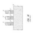
- photolithographyis first used to form a pattern of lines 10 in a photoresist layer overlying a layer 20 of an expendable material and a substrate 30 .
- the patternis then transferred by an etch step (preferably anisotropic) to the layer 20 , forming placeholders, or mandrels, 40 .
- the photoresist lines 10can be stripped and the mandrels 40 can be isotropically etched to increase the distance between neighboring mandrels 40 , as shown in FIG. 1C .
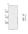
- a layer 50 of materialis subsequently deposited over the mandrels 40 , as shown in FIG. 1D .
- Spacers 60i.e., material extending or originally formed extending from sidewalls of another material, are then formed on the sides of the mandrels 40 by preferentially etching the spacer material from the horizontal surfaces 70 and 80 in a directional spacer etch, as shown in FIG. 1E .
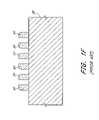
- the remaining mandrels 40are then removed, leaving behind only the spacers 60 , which together act as a mask for patterning, as shown in FIG. 1F .
- the same widthnow includes two features and two spaces defined by the spacers 60 .
- the smallest feature size possible with a photolithographic techniqueis effectively decreased.
- pitch doublingthis reduction in pitch is conventionally referred to as pitch “doubling,” or, more generally, pitch “multiplication.” That is, conventionally “multiplication” of pitch by a certain factor actually involves reducing the pitch by that factor.
- pitch “doubling”this reduction in pitch is conventionally referred to as pitch “doubling,” or, more generally, pitch “multiplication.” That is, conventionally “multiplication” of pitch by a certain factor actually involves reducing the pitch by that factor.
- pitch “doubling”pitch “multiplication” of pitch by a certain factor actually involves reducing the pitch by that factor.
- the layer 50 of spacer materialtypically has a single thickness 90 (see FIGS. 1D and 1E ) and because the sizes of the features formed by the spacers 60 usually corresponds to that thickness 90 , pitch doubling typically produces features of only one width.
- Circuitstypically employ features of different sizes.
- random access memory circuitstypically contain arrays of memory cells and logic circuits in the so-called “periphery.” In the arrays, the memory cells are typically connected by conductive lines and, in the periphery, the conductive lines typically contact landing pads for connecting arrays to logic. Peripheral features such as landing pads, however, can be larger than the conductive lines.
- periphery electrical devicessuch as transistors can be larger than electrical devices in the array.
- peripheral featurescan be formed with the same pitch as the array, the flexibility required to define circuits will typically not be possible using a single mask, particularly if the patterns are limited to those that can be formed along the sidewalls of patterned photoresist.
- Some proposed methods for forming patterns at the periphery and at the arrayinvolve etching a pattern into the array region of a substrate and into periphery of the substrate separately. Thus, a pattern in the array is first formed and transferred to the substrate using one mask and then another pattern in the periphery is formed and separately transferred to the substrate using another mask. Because such methods form patterns using different masks at different locations on a substrate, they are limited in their ability to form features that require overlapping patterns, such as when a landing pad overlaps an interconnect line, and yet a third mask may be necessitated to “stitch” two separate patterns with interconnects. Additionally, such a third mask would face even greater challenges with respect to mask alignment due to the fine features defined by the pitch multiplication technique.
- a methodfor semiconductor processing.
- the methodcomprises providing a substrate having a primary mask layer overlying the substrate, a temporary layer overlying the primary mask layer and a first photoresist layer overlying the temporary layer.
- a photoresist patternis formed in the first photoresist layer.
- a first pattern, having features derived from features of the photoresist pattern,is formed in the temporary layer.
- a second photoresist layeris subsequently formed above the level of the first pattern and an other photoresist pattern is formed in the second photoresist layer.
- the other photoresist pattern and the first patternare transferred to the primary mask layer to form a mixed pattern in the primary mask layer.
- the substrateis processed through the mixed pattern in the primary mask layer. It will be appreciated that the substrate can comprise any material or materials to be processed through the primary masking layer.
- a methodfor forming an integrated circuit. The method comprises providing a substrate and forming an amorphous carbon layer over the substrate. A first hard mask layer is formed over the first amorphous carbon layer. A temporary layer is formed over the first hard mask layer and a second hard mask layer is formed over the temporary layer.
- a methodfor semiconductor fabrication.
- the methodcomprises forming a first pattern by pitch multiplication and separately forming a second pattern by photolithography without pitch multiplication.
- the first and second patternsare transferred to a mask layer and a substrate is etched through the mask layer.
- a methodfor forming an integrated circuit.
- the methodcomprises forming a mask pattern in which a first part of the mask pattern has a first pitch and a second part of the mask pattern has a second pitch.
- the first pitchis below a minimum pitch of a photolithographic technique for defining the second pattern.
- the methodalso comprises etching a substrate through the mask pattern.
- a methodfor forming a memory device.
- the methodcomprises forming a pattern of temporary placeholders in a layer over a first carbon layer.
- a layer of mask materialis deposited over surfaces of the temporary placeholders and is then selectively removed from horizontal surfaces of the memory device.
- the temporary placeholdersare selectively removed relative to the mask material to form a pattern of mask material corresponding to features in an array region of the memory device.
- a methodfor for manufacturing an integrated circuit.
- the methodcomprises forming a plurality of mandrel strips.
- a spaceris formed on sidewalls of each mandrel strip.
- the mandrel stripsare removed to form a pattern of spaced apart spacers.
- a mask layeris formed in a plane above the spacers and a pattern is formed in the mask layer. The pattern is transferred to the same horizontal plane as the spacers.
- a methodfor manufacturing an integrated circuit.
- the methodcomprises providing a plurality of spaced-apart lines of a mask material above a substrate, where the mask material is different from photoresist.
- a plurality of featuresis defined in a photodefinable material above the substrate by a photolithographic technique.
- the spaced-apart lines and the plurality of featuresare replicated in an amorphous carbon layer below the spaced-apart lines.
- a methodfor forming a mask pattern to fabricate an integrated circuit.
- the methodcomprises providing a plurality of lines of a first mask material.
- the linesare separated by a first temporary material.
- the first temporary materialis selectively etched.
- Spaces between the linesare filled with a second temporary material.
- the second temporary materialis selectively etched to open the spaces.
- a patternis then formed in a layer of another mask material below the plurality of lines by selectively etching through the spaces.
- a processfor fabricating an integrated circuit.
- the processcomprises providing a masking layer extending over a first and a second region of a partially fabricated integrated circuit.
- a patternis formed in the masking layer.
- a minimum feature size of a portion of the pattern corresponding to the first regionis equal to or less than about half a minimum feature size of an other portion of the pattern corresponding to the second region.
- a partially formed integrated circuitcomprises a carbon layer and a plurality of pitch-multiplied spacers on a level overlying the carbon layer.
- the spacershave a pitch of about 100 nm or less.
- a partially formed integrated circuitcomprises a substrate and a primary mask layer overlying the substrate.
- the primary mask layerformed of a material different from photoresist.
- a mask material defining a first patternis disposed in a first plane overlying the primary mask layer.
- a photodefinable material defining a second patternis disposed in a second plane overlying the mask material.
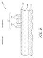
- FIGS. 1A–1Fare schematic, cross-sectional side views of partially formed conductive lines, formed in accordance with a prior art pitch doubling method
- FIGS. 2A–2Bare a schematic, cross-sectional top and side views of a partially formed memory device, in accordance with preferred embodiments of the invention.
- FIG. 3is a schematic, cross-sectional side view of the partially formed memory device of FIG. 2 after forming lines in a selectively definable layer in the array of the memory device, in accordance with preferred embodiments of the invention;
- FIG. 4is a schematic, cross-sectional side view of the partially formed memory device of FIG. 3 after widening spaces between photoresist lines, in accordance with preferred embodiments of the invention
- FIG. 5is a schematic, cross-sectional side view of the partially formed memory device of FIG. 4 after etching through a hard mask layer, in accordance with preferred embodiments of the invention
- FIG. 6is a schematic, cross-sectional side view of the partially formed memory device of FIG. 5 after transferring a pattern from the photoresist layer to a temporary layer, in accordance with preferred embodiments of the invention
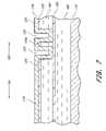
- FIG. 7is a schematic, cross-sectional side view of the partially formed memory device of FIG. 6 after depositing a layer of a spacer material, in accordance with preferred embodiments of the invention.
- FIG. 8is a schematic, cross-sectional side view of the partially formed memory device of FIG. 7 after a spacer etch, in accordance with preferred embodiments of the invention.
- FIG. 9is a schematic, cross-sectional side view of the partially formed memory device of FIG. 8 after removing a remaining portion of the temporary layer to leave a pattern of spacers in the array of the memory device, in accordance with preferred embodiments of the invention.
- FIG. 10is a schematic, cross-sectional side view of the partially formed memory device of FIG. 9 after surrounding the spacers with a removable material and forming a hard mask layer and a selectively definable layer over the spacers, in accordance with preferred embodiments of the invention;
- FIG. 11is a schematic, cross-sectional side view of the partially formed memory device of FIG. 10 after forming a pattern in the selectively definable layer in the periphery of the memory device, in accordance with preferred embodiments of the invention;
- FIG. 12is a schematic, cross-sectional side view of the partially formed memory device of FIG. 11 after etching through the top hard mask layer, in accordance with preferred embodiments of the invention.
- FIG. 13is a schematic, cross-sectional side view of the partially formed memory device of FIG. 12 after transferring the pattern from the selectively definable layer to the same level as the spacers, in accordance with preferred embodiments of the invention;
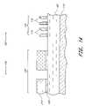
- FIG. 14is a schematic, cross-sectional side view of the partially formed memory device of FIG. 13 after etching the pattern in the periphery and the spacer pattern in the array into an underlying hard mask layer, in accordance with preferred embodiments of the invention;
- FIG. 15is a schematic, cross-sectional side view of the partially formed memory device of FIG. 14 after transferring the pattern in the periphery and the spacer pattern in the array together to a primary mask layer, in accordance with preferred embodiments of the invention;
- FIG. 16is a schematic, cross-sectional side view of the partially formed memory device of FIG. 15 after transferring the periphery pattern and the spacer pattern to the underlying substrate, in accordance with preferred embodiments of the invention.
- FIGS. 17A and 17Bare micrographs, as viewed through a scanning electron microscope, of a pattern etched into the array and the periphery, respectively, of a partially formed memory device, formed in accordance with preferred embodiments of the invention.
- pitch doubling techniquescan have difficulty transferring spacer patterns to a substrate.
- both the spacers and the underlying substrateare exposed to an etchant, which preferentially etches away the substrate material.
- the etchantsalso wear away the spacers, albeit at a slower rate.
- the spacerscan be worn away by the etchant before the pattern transfer is complete.
- the spacer and second patternsare then transferred from the primary masking layer to the underlying substrate in a single step.
- patterns for forming different size featuressome of which are below the minimum pitch of the photolithographic technique used for patterning, can be formed and these patterns can be successfully transferred to the underlying substrate.
- the second patternis initially formed on a layer overlying the spacer pattern, the second pattern can overlap the spacer pattern.
- overlapping features of different sizessuch as conducting lines and landing pads or periphery transistors, can advantageously be formed.
- the primary masking layeris the masking layer that directly overlies and, due to etch selectivity, is primarily used to perform a process (e.g., etch) on the substrate through the primary masking layer.
- the primary masking layeris preferably formed of a material that allows good etch selectivity relative to both the spacer material and the substrate material, so that spacer pattern can effectively be transferred to it; so that the primary masking layer can be selectively removed after processing without harming the substrate; and, when the mask is used for etching the substrate, so that the pattern in it can effectively be transferred to the substrate. Due to its excellent etch selectivity relative to a variety of materials, including oxides, nitrides and silicon, the primary masking layer is preferably formed of carbon and, more preferably, amorphous carbon.
- a substratecan comprise any material or materials that are to be processed through the primary masking layer.
- a substratecan include a layer of a single material, a plurality of layers of different materials, a layer or layers having regions of different materials or structures in them, etc. These materials can include semiconductors, insulators, conductors, or combinations thereof.
- the substratecomprises structures or layers ultimately form part of the integrated circuit being fabricated.
- transferring a pattern from a first level to a second levelinvolves forming features in the second level that generally correspond to features on the first level.
- the path of lines in the second levelwill generally follow the path of lines on the first level and the location of other features on the second level will correspond to the location of similar features on the first level.
- the precise shapes and sizes of featurescan vary from the first level to the second level, however. For example, depending upon etch chemistries and conditions, the sizes of and relative spacings between the features forming the transferred pattern can be enlarged or diminished relative to the pattern on the first level, while still resembling the same initial “pattern.”
- FIGS. 2–16are not necessarily drawn to scale.
- part of the pattern to be transferred to a substrateis formed by pitch multiplication and that has a pitch below the minimum pitch of the photolithographic technique used for processing the substrate.
- the preferred embodimentscan be used to form any integrated circuit, they are particularly advantageously applied to form devices having arrays of electrical devices, including logic or gate arrays and volatile and non-volatile memory devices such as DRAM, ROM or flash memory.
- pitch multiplicationcan be used to form, e.g., transistor gate electrodes and conductive lines in the array region of the chips, while conventional photolithography can be used to form larger features, such as contacts, at the peripheries of the chips. Exemplary masking steps in the course of fabricating a memory chip are illustrated in the Figures.
- FIG. 2Ashows a top view of a partially fabricated integrated circuit, or memory chip, 100 .
- a central region 102the “array,” is surrounded by a peripheral region 104 , the “periphery.”
- the array 102will typically be densely populated with conducting lines and electrical devices such as transistors and capacitors.
- pitch multiplicationcan be used to form features in the array 102 , as discussed below.
- the periphery 104can have features larger than those in the array 102 .
- Conventional photolithography, rather than pitch multiplicationis typically used to pattern these features, because the geometric complexity of logic circuits located in the periphery 104 makes using pitch multiplication difficult.
- some devices in the peripheryrequire larger geometries due to electrical constraints, thereby making pitch multiplication less advantageous than conventional photolithography for such devices.
- a partially formed integrated circuit 100is provided.
- a substrate 110is provided below various layers 120 – 160 .
- the substrate 110will be patterned to form various features and the layers 120 – 160 will be etched to form a mask for the pattern, as discussed below.
- the materials for the layers overlying the substrate 110are preferably chosen based upon consideration of the chemistry and process condition requirements for the various pattern forming and pattern transferring steps discussed herein.
- the layers between a topmost selectively definable layer 120which preferably is definable by a lithographic process, and the substrate 110 function to transfer a pattern derived from the selectively definable layer 120 to the substrate 110
- the layers between the selectively definable layer 120 and the substrate 110are preferably chosen so that they can be selectively etched relative to other exposed materials during their etch. It will be appreciated that a material is considered selectively, or preferentially, etched when the etch rate for that material is at least about 5 times greater, preferably about 10 times greater, more preferably about 20 times greater and, most preferably, at least about 40 times greater than that for surrounding materials.
- the selectively definable layer 120overlies a first hard mask, or etch stop, layer 130 , which overlies a temporary layer 140 , which overlies a second hard mask, or etch stop, layer 150 , which overlies a primary mask layer 160 , which overlies the substrate 110 to be processed (e.g., etched) through a mask.
- the thicknesses of the layersare preferably chosen depending upon compatibility with the etch chemistries and process conditions described herein. For example, when transferring a pattern from an overlying layer to an underlying layer by selectively etching the underlying layer, materials from both layers are removed to some degree.
- the upper layeris preferably thick enough so that it is not worn away over the course of the etch.
- the first hard mask layer 130is preferably between about 10–50 nm thick and, more preferably, between about 10–30 nm thick.
- the temporary layer 140is preferably between about 100–300 nm thick and, more preferably, between about 100–200 nm thick.
- the second hard mask layer 150is preferably between about 10–50 nm thick and, more preferably, about 20–40 nm thick and the primary mask layer 160 is preferably between about 100–1000 nm thick and, more preferably, about 100–500 nm thick.
- the selectively definable layer 120is preferably formed of a photoresist, including any photoresist known in the art.
- the photoresistcan be any photoresist compatible with 13.7 nm, 157 nm, 193 nm, 248 nm or 365 nm wavelength systems, 193 nm wavelength immersion systems or electron beam lithographic systems.
- preferred photoresist materialsinclude argon fluoride (ArF) sensitive photoresist, i.e., photoresist suitable for use with an ArF light source, and krypton fluoride (KrF) sensitive photoresist, i.e., photoresist suitable for use with a KrF light source.
- ArFargon fluoride
- KrFkrypton fluoride
- ArF photoresistsare preferably used with photolithography systems utilizing relatively short wavelength light, e.g., 193 nm.
- KrF photoresistsare preferably used with longer wavelength photolithography systems, such as 248 nm systems.
- the layer 120 and any subsequent resist layerscan be formed of a resist that can be patterned by nano-imprint lithography, e.g., by using a mold or mechanical force to pattern the resist.
- the material for the first hard mask layer 130preferably comprises a silicon oxide (SiO 2 ), silicon or a dielectric anti-reflective coating (DARC), such as a silicon-rich silicon oxynitride.
- DARCscan be particularly advantageous for forming patterns having pitches near the resolution limits of a photolithographic technique because they can enhance resolution by minimizing light reflections. It will be appreciated that light reflections can decrease the precision with which photolithography can define the edges of a pattern.
- a bottom anti-reflective coating (BARC)(not shown) can similarly be used in addition to the first hard mask layer 130 to control light reflections.
- the temporary layer 140is preferably formed of amorphous carbon, which offers very high etch selectivity relative to the preferred hard mask materials. More preferably, the amorphous carbon is a form of transparent carbon that is highly transparent to light and which offers further improvements for photo alignment by being transparent to wavelengths of light used for such alignment. Deposition techniques for forming a highly transparent carbon can be found in A. Helmbold, D. Meissner, Thin Solid Films, 283 (1996) 196–203, the entire disclosure of which is incorporated herein by reference.
- the second hard mask layer 150preferably comprises a dielectric anti-reflective coating (DARC) (e.g., a silicon oxynitride), a silicon oxide (SiO 2 ) or silicon.
- DARCdielectric anti-reflective coating
- BARCbottom anti-reflective coating
- first and the second hard mask layers 130 and 150can be formed of different materials, these layers are preferably formed of the same material for ease of processing and to minimize the number of different etch chemistries utilized, as described below.
- the primary mask layer 160is preferably formed of amorphous carbon and, more preferably, transparent carbon.
- various layers discussed hereincan be formed by various methods known to those of skill in the art.
- various vapor deposition processessuch as chemical vapor deposition can be used to form the hard mask layers.
- a low temperature chemical vapor deposition processis used to deposit the hard mask layers or any other materials, e.g., spacer material ( FIG. 7 ), over the mask layer 160 , where the mask layer 160 is formed of amorphous silicon.
- Such low temperature deposition processesadvantageously prevent chemical or physical disruption of the amorphous carbon layer.
- amorphous carbon layerscan be formed by chemical vapor deposition using a hydrocarbon compound, or mixtures of such compounds, as carbon precursors.
- exemplary precursorsinclude propylene, propyne, propane, butane, butylene, butadiene and acetelyne.
- a suitable method for forming amorphous carbon layersis described in U.S. Pat. No. 6,573,030 B1, issued to Fairbaim et al. on Jun. 3, 2003, the entire disclosure of which is incorporated herein by reference.
- pitch multiplication in the array of the partially formed integrated circuit 100is performed.
- a patternis formed on the photodefinable layer 120 , as shown in FIG. 3 .
- the photodefinable layer 120can be patterned by, e.g., photolithography, in which the layer 120 is exposed to radiation through a reticle and then developed. After being developed, the remaining photodefinable material, photoresist in this case, comprises lines 122 , which define spaces 124 .
- the widths of the spaces 122 and the photoresist lines 122can be altered to a desired dimension.
- the spaces 122can be widened by etching the photoresist lines 124 .
- the photoresist lines 124are preferably etched using an isotropic etch, such as a sulfur oxide plasma, e.g., a plasma comprising SO 2 , O 2 , N 2 and Ar.
- the extent of the etchis preferably selected so that a resulting line 124 a has a width corresponding to the desired spacing of the spacers to be formed, as will be appreciated from the discussion below with respect to FIGS. 8–16 .
- this etchcan smooth the edges of the lines 124 thereby improving the uniformity of the lines 124 .
- the resulting photoresist lines 124 and 124 athus constitute the placeholders or mandrels upon which a pattern of spacers 175 ( FIG. 9 ) will be formed.
- the spaces between the spaces 122can be narrowed by expanding the lines 124 to a desired size. For example, additional material can be deposited over the lines 124 or the lines 124 can be chemically reacted to form a material having a larger volume to increase their size.
- the pattern of the (modified) photodefinable layer 120is preferably transferred to a layer 140 of material that can withstand with the process conditions for spacer material deposition, discussed below.
- the material forming the temporary layer 140is preferably selected such that it can be selectively removed relative to the spacer material and the underlying layer.
- the layer 140is preferably formed of amorphous carbon. Because the preferred chemistries for etching photoresist also typically etch significant amounts of amorphous carbon and because chemistries are available for etching amorphous carbon with excellent selectivity relative to a variety of materials, a hard mask layer 130 selected from such materials preferably separates the layers 120 and 140 . Suitable materials for the hard mask layer 130 include, for example, DARCs, silicon oxides or nitrides, and silicon.
- the pattern in the photodefinable layer 120is preferably transferred to the hard mask layer 130 , as shown in FIG. 5 .
- This transferis preferably accomplished using an anisotropic etch, such as an etch using a fluorocarbon plasma, although a wet (isotropic) etch may also be suitable if the hard mask layer 130 is thin.
- Preferred fluorocarbon plasma etch chemistriescan include CF 4 , CFH 3 , CF 2 H 2 , CF 3 H, etc.
- the patternis then transferred to the temporary layer 140 , as shown in FIG. 6 , preferably using a SO 2 -containing plasma, e.g., a plasma containing SO 2 , O 2 and Ar.
- a SO 2 -containing plasmae.g., a plasma containing SO 2 , O 2 and Ar.
- the SO 2 -containing plasmacan etch carbon of the preferred temporary layer 140 at a rate greater than 20 times and, more preferably, greater than 40 times the rate that the hard mask layer 130 is etched.
- a suitable SO 2 -contaiing plasmais described in U.S. patent application Ser. No. 10/931,772 to Abatchev et al., filed Aug. 31, 2004, entitled Critical Dimension Control, the entire disclosure of which is incorporate herein by reference. It will be appreciated that the SO 2 -containing plasma simultaneously etches the temporary layer 140 and removes the photodefinable layer 120 .
- a layer 170 of spacer materialis preferably next deposited over the hard mask layer 130 and the temporary layer 140 .
- the spacer materialis preferably deposited by chemical vapor deposition or atomic layer deposition.
- the spacer materialcan be any material capable of use as a mask to transfer a pattern to the underlying primary mask layer 160 .
- the spacer materialpreferably: 1) can be deposited with good step coverage, 2) can be deposited at a low temperature compatible with the temporary layer 140 and 3) can be selectively etched relative to the temporary layer 140 and any layer underlying the temporary layer 140 .
- Preferred materialsinclude silicon nitrides and silicon oxides.
- the spacer layer 170is then subjected to an anisotropic etch to remove spacer material from horizontal surfaces 180 of the partially formed integrated circuit 100 .
- an etchalso known as a spacer etch
- a fluorocarbon plasmawhich can also advantageously etch the hard mask layer 130 .
- the amorphous carbon layer 140can be selectively removed, using, e.g., a SO 2 -containing plasma.
- FIG. 9shows a pattern of spacers 175 left after the amorphous carbon etch.
- pitch multiplication in the array of the partially formed integrated circuit 100has been accomplished and, in the illustrated embodiment, the pitch of the spacers is half that of the photoresist lines 124 ( FIG. 3 ) originally formed by photolithography. It will be appreciated that the spacers 175 generally follow the outline of the pattern or lines 124 originally formed in the photodefinable layer 120 .
- a second patternis formed at the periphery 104 .
- the spacers 175are protected and another photodefinable layer 220 is formed, as shown in FIG. 10 , to allow for patterning of the second pattern at the periphery 104 .
- the spacers 175are protected by forming a protective layer 200 over the spacers 175 .
- the protective layer 200is preferably at least as tall as the spacers 175 and preferably about 100–500 nm thick and, more preferably, about 100–300 nm thick.
- a hard mask layer 210is next preferably formed over the protective layer 200 to aid in transferring a pattern from the photodefinable layer 220 to the protective layer 200 .
- the hard mask layer 210is about 40–80 nm thick and, more preferably, about 50–60 nm thick.
- the protective layer 200is preferably formed of a material that is readily removed selectively relative to the spacers 175 .
- the protective layer 200can be formed of a photoresist, and may be the same or a different photoresist from that used to form the photodefinable layer 120 ( FIGS. 2–5 ), which can be the same or a different material from than used to form the photodefinable layer 220 ( FIG. 10 ).
- the protective layer 200is formed of amorphous carbon, which can be etched with excellent selectivity relative to the spacers 175 .
- the hard mask layer 210can be omitted.
- the protective layer 200can be formed of a bottom anti-reflective coating (BARC) and a photoresist can be formed directly above the BARC.
- the spacers 175can be formed of a material which allows good etch selectivity to the BARC, including silicon nitrides or oxides.
- the photodefinable layer 220is preferably patterned using the same photolithographic technique used to pattern the photodefinable layer 120 .
- a pattern 230is formed in the photodefinable layer 220 .
- the pattern 177preferably has a pitch or resolution smaller than the minimum pitch or resolution of the photolithographic technique
- the pattern 230preferably has a pitch or resolution equal to or greater than the minimum pitch or resolution of the photolithographic technique.
- the pattern 230 at the periphery 104can be used to form landing pads, transistors, local interconnects etc.
- the pattern 230can also overlap the pattern 177 .
- the use of different reference numerals ( 177 and 230 ) for these patternsindicates that they were originally formed in different steps.
- the pattern 230is then transferred to the same level as the pattern 177 of spacers 175 .
- the hard mask layer 210is selectively etched relative to the photodefinable layer 220 , preferably using an anisotropic etch such as a fluorocarbon plasma etch. Alternatively, a wet (isotropic) etch may also be suitable for the hard mask layer 210 is appropriately thin.
- the pattern 230is then transferred to the protective layer 200 by another anisotropic etch, such as an etch with a SO 2 -containing plasma, as shown in FIG. 13 . Because the hard mask layer 210 overlying the spacers 175 has previously been removed, this etch also removes the protective layer 200 around the spacers 175 , thereby leaving those spacers 175 exposed.
- the patterns 177 and 230are then transferred down to the primary mask layer 160 , which preferably comprises a material having good etch selectivity to the substrate 110 , and vice versa, to allow the patterns 177 and 230 to be simultaneously transferred to the substrate 110 .
- the patterns 177 and 230form a mixed pattern in the primary mask layer 160 .
- the hard mask layer 150 overlying the primary mask layer 160is first etched ( FIG. 14 ).
- the hard mask layer 150is preferably anisotropically etched, preferably using a fluorocarbon plasma. Alternatively, an isotropic etch may be used if the hard mask layer 150 is relatively thin.
- the primary mask layer 160is then anisotropically etched, preferably using a SO 2 -containing plasma, which can simultaneously remove the photodefinable layer 200 ( FIG. 15 ).
- the SO 2 -containing plasmahas excellent selectivity for the amorphous carbon of the primary mask layer 160 relative to the hard mask layer 150 .
- a thick enough maskcan be formed in the primary mask layer 160 to later effectively transfer the mask pattern to the substrate 110 using conventional etch chemistries and without wearing away the primary mask layer 160 before the pattern transfer is complete.
- the patterns 177 and 230can then be transferred to the subtrate 110 using the layer 160 as a mask, as illustrated in FIG. 16 .
- the pattern transfercan be readily accomplished using conventional etches appropriate for the material or materials comprising the substrate 110 .
- a fluorocarbon etchcomprising CF 4 , CHF 3 and/or NF 3 containing plasma can be used to etch silicon nitride
- a fluorocarbon etchcomprising CF 4 , CHF 3 , CH 2 F 2 and/or C 4 F 8 containing plasma can be used to etch silicon oxide and a HBr, Cl 2 , NF 3 , SF 6 and/or CF 4 containing plasma etch can be used to etch silicon.
- the skilled artisancan readily determine suitable etch chemistries for other substrate materials, such as conductors, including aluminum, transition metals, and transition metal nitrides.
- an aluminum substratecan be etched using a fluorocarbon etch.
- the substrate 110comprises layers of different materials
- a succession of different chemistriespreferably dry-etch chemistries
- the spacers 175 and the hard mask layer 150may be etched.
- Amorphous carbon of the primary mask layer 160advantageously offers excellent resistance to conventional etch chemistries, especially those used for etching silicon-containing materials.
- the primary mask layer 160can effectively be used as a mask for etching through a plurality of substrate layers, or for forming high aspect ratio trenches.
- the pitch doubled pattern 177 and the pattern 230 formed by conventional lithographycan simultaneously be transferred to the substrate 110 , or each individual layer of the substrate 110 , in a single etch step.
- FIGS. 17A and 17Bshow the resultant structure.
- FIG. 17Ashows the array portion of the integrated circuit 100
- FIG. 17Bshows the periphery of the integrated circuit 100 ( FIGS. 2–16 ).
- the substrate 110can be any layer of material or materials that the patterns 177 and 230 are etched into.
- the composition of the substrate 110can depend upon, e.g., the electrical device to be formed.
- the substrate 110comprises a Si 3 N 4 layer 110 a , a polysilicon layer 110 b , a SiO 2 layer 110 c and a silicon layer 110 d .
- Such an arrangement of layerscan be advantageously used in the formation of, e.g., transistors.
- the etched surfacesexhibit exceptionally low edge roughness.
- the trenches formed in the arrayshow excellent uniformity, even at the low 100 nm pitch pictured.
- these resultsare achieved while also forming well-defined and smooth lines in the periphery, as illustrated in FIG. 17B .
- patterns according to the preferred embodimentsoffers numerous advantages. For example, because multiple patterns, with different size features, can be consolidated on a single final mask layer before being transferred to a substrate, overlapping patterns can easily be transferred to the substrate. Thus, pitch-doubled features and features formed by conventional photolithography can easily be formed connected to each other. Moreover, as evident in FIGS. 17A and 17B , exceptionally small features can be formed, while at the same time achieving exceptional and unexpectedly low line edge roughness. While not limited by theory, it is believed that such low line edge roughness is the result of the use of the layers 140 and 160 .
- Forming the spacers 175 and performing multiple anisotropic etches to transfer the patterns 177 and 230 from the level of the temporary layer 140 to the primary mask layer 160 and then to the substrate 110are believed to beneficially smooth the surfaces of the features forming the patterns 177 and 230 .
- the preferred amorphous carbon etch chemistries disclosed hereinallow the use of thin hard mask layers, such as the layers 130 and 150 , relative to the depth that underlying amorphous carbon layers, such as the layers 140 and 160 , are etched.
- layerse.g., photoresist layers
- pitch multiplied patternstypically formed closed loops, since the patterns are formed by spacers that surround a mandrel. Consequently, where the pitch multiplied pattern is used to form conductive lines, additional processing steps are preferably used to cut off the ends of these loops, so that each loop forms two individual, non-connected lines.
- the various hard mask layersare preferably each formed of the same material, as are the primary mask layers.
- such an arrangementreduces processing complexity.
- the pitch of the pattern 177can be more than doubled.
- the pattern 177can be further pitch multiplied by forming spacers around the spacers 175 , then removing the spacers 175 , then forming spacers around the spacers that were formerly around the spacers the 175 , and so on.
- An exemplary method for further pitch multiplicationis discussed in U.S. Pat. No. 5,328,810 to Lowrey et al.
- the preferred embodimentscan advantageously be applied to formed patterns having both pitch multiplied and conventionally photolithographically defined features, the patterns 177 and 230 can both be pitch multiplied or can have different degrees of pitch multiplication.
- more than two patterns 177 and 230can be consolidated on the primary mask layer 160 if desired.
- additional mask layerscan be deposited between the layers 140 and 160 .
- the patterns 177 and 230can be transferred to an additional mask layer overlying the hard mask layer 150 and then the sequence of steps illustrated in FIGS. 10–16 can be performed to protect the patterns 77 and 230 , to form the new pattern in an overlying photodefinable layer and to transfer the patterns to the substrate 110 .
- the additional mask layerpreferably comprises a material that can be selectively etched relative to the hard mask layer 150 and a protective layer that surrounds the patterns 177 and 230 after being transferred to the additional mask layer.
- processing through the various mask layerscan involve subjecting layers underlying the mask layers to any semiconductor fabrication process.
- processingcan involve ion implantation, diffusion doping, depositing, or wet etching, etc. through the mask layers and onto underlying layers.
- the mask layerscan be used as a stop or barrier for chemical mechanical polishing (CMP) or CMP can be performed on the mask layers to allow for both planarizing of the mask layers and etching of the underlying layers,
Landscapes
- Engineering & Computer Science (AREA)
- Physics & Mathematics (AREA)
- Condensed Matter Physics & Semiconductors (AREA)
- General Physics & Mathematics (AREA)
- Manufacturing & Machinery (AREA)
- Computer Hardware Design (AREA)
- Microelectronics & Electronic Packaging (AREA)
- Power Engineering (AREA)
- Chemical & Material Sciences (AREA)
- Inorganic Chemistry (AREA)
- Analytical Chemistry (AREA)
- Drying Of Semiconductors (AREA)
- Internal Circuitry In Semiconductor Integrated Circuit Devices (AREA)
- Semiconductor Memories (AREA)
- Light Receiving Elements (AREA)
- Exposure And Positioning Against Photoresist Photosensitive Materials (AREA)
Abstract
Description
Claims (16)
Priority Applications (13)
| Application Number | Priority Date | Filing Date | Title |
|---|---|---|---|
| US10/934,778US7115525B2 (en) | 2004-09-02 | 2004-09-02 | Method for integrated circuit fabrication using pitch multiplication |
| KR1020077007511AKR100879499B1 (en) | 2004-09-02 | 2005-08-26 | Integrated circuit fabrication method using pitch multiplication |
| EP05813972AEP1789997A2 (en) | 2004-09-02 | 2005-08-26 | Method for integrated circuit fabrication using pitch multiplication |
| EP10075082AEP2219207A1 (en) | 2004-09-02 | 2005-08-26 | Method for integrated circuit fabrication using pitch multiplication |
| CNA2005800357643ACN101044596A (en) | 2004-09-02 | 2005-08-26 | Integrated circuit fabrication method using pitch multiplication |
| JP2007530349AJP4945802B2 (en) | 2004-09-02 | 2005-08-26 | Integrated circuit manufactured using pitch multiplication and method of manufacturing the same |
| PCT/US2005/031094WO2006026699A2 (en) | 2004-09-02 | 2005-08-26 | Method for integrated circuit fabrication using pitch multiplication |
| SG200801703-0ASG140614A1 (en) | 2004-09-02 | 2005-08-26 | Method for integrated circuit fabrication using pitch multiplication |
| TW094130195ATWI278020B (en) | 2004-09-02 | 2005-09-02 | Method for integrated circuit fabrication using pitch multiplication |
| US11/492,513US7629693B2 (en) | 2004-09-02 | 2006-07-24 | Method for integrated circuit fabrication using pitch multiplication |
| US11/492,323US7547640B2 (en) | 2004-09-02 | 2006-07-24 | Method for integrated circuit fabrication using pitch multiplication |
| US11/683,518US7687408B2 (en) | 2004-09-02 | 2007-03-08 | Method for integrated circuit fabrication using pitch multiplication |
| US12/707,560US8216949B2 (en) | 2004-09-02 | 2010-02-17 | Method for integrated circuit fabrication using pitch multiplication |
Applications Claiming Priority (1)
| Application Number | Priority Date | Filing Date | Title |
|---|---|---|---|
| US10/934,778US7115525B2 (en) | 2004-09-02 | 2004-09-02 | Method for integrated circuit fabrication using pitch multiplication |
Related Child Applications (3)
| Application Number | Title | Priority Date | Filing Date |
|---|---|---|---|
| US11/492,323DivisionUS7547640B2 (en) | 2004-09-02 | 2006-07-24 | Method for integrated circuit fabrication using pitch multiplication |
| US11/492,323ContinuationUS7547640B2 (en) | 2004-09-02 | 2006-07-24 | Method for integrated circuit fabrication using pitch multiplication |
| US11/492,513DivisionUS7629693B2 (en) | 2004-09-02 | 2006-07-24 | Method for integrated circuit fabrication using pitch multiplication |
Publications (2)
| Publication Number | Publication Date |
|---|---|
| US20060046484A1 US20060046484A1 (en) | 2006-03-02 |
| US7115525B2true US7115525B2 (en) | 2006-10-03 |
Family
ID=35943911
Family Applications (5)
| Application Number | Title | Priority Date | Filing Date |
|---|---|---|---|
| US10/934,778Expired - Fee RelatedUS7115525B2 (en) | 2004-09-02 | 2004-09-02 | Method for integrated circuit fabrication using pitch multiplication |
| US11/492,323Expired - Fee RelatedUS7547640B2 (en) | 2004-09-02 | 2006-07-24 | Method for integrated circuit fabrication using pitch multiplication |
| US11/492,513Expired - Fee RelatedUS7629693B2 (en) | 2004-09-02 | 2006-07-24 | Method for integrated circuit fabrication using pitch multiplication |
| US11/683,518Expired - Fee RelatedUS7687408B2 (en) | 2004-09-02 | 2007-03-08 | Method for integrated circuit fabrication using pitch multiplication |
| US12/707,560Expired - Fee RelatedUS8216949B2 (en) | 2004-09-02 | 2010-02-17 | Method for integrated circuit fabrication using pitch multiplication |
Family Applications After (4)
| Application Number | Title | Priority Date | Filing Date |
|---|---|---|---|
| US11/492,323Expired - Fee RelatedUS7547640B2 (en) | 2004-09-02 | 2006-07-24 | Method for integrated circuit fabrication using pitch multiplication |
| US11/492,513Expired - Fee RelatedUS7629693B2 (en) | 2004-09-02 | 2006-07-24 | Method for integrated circuit fabrication using pitch multiplication |
| US11/683,518Expired - Fee RelatedUS7687408B2 (en) | 2004-09-02 | 2007-03-08 | Method for integrated circuit fabrication using pitch multiplication |
| US12/707,560Expired - Fee RelatedUS8216949B2 (en) | 2004-09-02 | 2010-02-17 | Method for integrated circuit fabrication using pitch multiplication |
Country Status (8)
| Country | Link |
|---|---|
| US (5) | US7115525B2 (en) |
| EP (2) | EP1789997A2 (en) |
| JP (1) | JP4945802B2 (en) |
| KR (1) | KR100879499B1 (en) |
| CN (1) | CN101044596A (en) |
| SG (1) | SG140614A1 (en) |
| TW (1) | TWI278020B (en) |
| WO (1) | WO2006026699A2 (en) |
Cited By (268)
| Publication number | Priority date | Publication date | Assignee | Title |
|---|---|---|---|---|
| US20060263699A1 (en)* | 2005-05-23 | 2006-11-23 | Mirzafer Abatchev | Methods for forming arrays of a small, closely spaced features |
| US20070215986A1 (en)* | 2006-03-15 | 2007-09-20 | Dirk Manger | Hard mask layer stack and a method of patterning |
| US20070224823A1 (en)* | 2006-03-23 | 2007-09-27 | Sandhu Gurtej S | Topography directed patterning |
| US20070281220A1 (en)* | 2006-06-02 | 2007-12-06 | Sandhu Gurtej S | Topography based patterning |
| US20080070165A1 (en)* | 2006-09-14 | 2008-03-20 | Mark Fischer | Efficient pitch multiplication process |
| US20080113483A1 (en)* | 2006-11-15 | 2008-05-15 | Micron Technology, Inc. | Methods of etching a pattern layer to form staggered heights therein and intermediate semiconductor device structures |
| KR100842753B1 (en)* | 2007-06-29 | 2008-07-01 | 주식회사 하이닉스반도체 | Pattern formation method of semiconductor device using spacer |
| US20080162781A1 (en)* | 2006-12-29 | 2008-07-03 | Gordon Haller | Method, apparatus, and system for flash memory |
| US20080206985A1 (en)* | 2007-02-28 | 2008-08-28 | Samsung Electronics Co., Ltd. | Method of fabricating a semiconductor device |
| US20080206898A1 (en)* | 2007-02-28 | 2008-08-28 | Kazuya Fukuhara | Pattern Monitor Mark and Monitoring Method Suitable for Micropattern |
| US20080239807A1 (en)* | 2005-11-25 | 2008-10-02 | Boaz Eitan | Transition areas for dense memory arrays |
| US20080261156A1 (en)* | 2003-12-26 | 2008-10-23 | Samsung Electronics Co., Ltd. | Method of forming a pattern in a semiconductor device and method of forming a gate using the same |
| US20080299465A1 (en)* | 2007-06-01 | 2008-12-04 | Bencher Christopher D | Frequency tripling using spacer mask having interposed regions |
| US20080299776A1 (en)* | 2007-06-01 | 2008-12-04 | Bencher Christopher D | Frequency doubling using spacer mask |
| US20080318032A1 (en)* | 2007-06-22 | 2008-12-25 | Hongbin Zhu | Method for selectively forming symmetrical or asymmetrical features using a symmetrical photomask during fabrication of a semiconductor device and electronic systems including the semiconductor device |
| US7476933B2 (en) | 2006-03-02 | 2009-01-13 | Micron Technology, Inc. | Vertical gated access transistor |
| US20090017627A1 (en)* | 2007-07-12 | 2009-01-15 | Joseph Neil Greeley | Methods of Modifying Oxide Spacers |
| US20090017631A1 (en)* | 2007-06-01 | 2009-01-15 | Bencher Christopher D | Self-aligned pillar patterning using multiple spacer masks |
| US20090032963A1 (en)* | 2007-08-03 | 2009-02-05 | Micron Technology, Inc. | Semiconductor structures including tight pitch contacts and methods to form same |
| US20090035584A1 (en)* | 2007-07-30 | 2009-02-05 | Micron Technology, Inc. | Methods for device fabrication using pitch reduction and associated structures |
| WO2009079517A2 (en) | 2007-12-18 | 2009-06-25 | Micron Technology, Inc. | Methods for isolating portions of a loop of pitch-multiplied material and related structures |
| US7566620B2 (en) | 2005-07-25 | 2009-07-28 | Micron Technology, Inc. | DRAM including a vertical surround gate transistor |
| US20090206336A1 (en)* | 2008-02-19 | 2009-08-20 | Dsm Solutions, Inc. | Method to fabricate gate electrodes |
| US20090240001A1 (en)* | 2008-03-21 | 2009-09-24 | Jennifer Kahl Regner | Methods of Improving Long Range Order in Self-Assembly of Block Copolymer Films with Ionic Liquids |
| US20090239382A1 (en)* | 2008-03-21 | 2009-09-24 | Micron Technology, Inc. | Method for selectively modifying spacing between pitch multiplied structures |
| US7601595B2 (en) | 2005-07-06 | 2009-10-13 | Micron Technology, Inc. | Surround gate access transistors with grown ultra-thin bodies |
| US20090263972A1 (en)* | 2008-04-04 | 2009-10-22 | Applied Materials, Inc. | Boron nitride and boron-nitride derived materials deposition method |
| US20090305152A1 (en)* | 2008-06-09 | 2009-12-10 | Ryoichi Inanami | Semiconductor device manufacturing method |
| US20090305497A1 (en)* | 2008-06-05 | 2009-12-10 | Mitsuhiro Omura | Method for fabricating semiconductor device |
| US20090311861A1 (en)* | 2008-06-17 | 2009-12-17 | Samsung Electronics Co., Ltd. | Methods of forming fine patterns in the fabrication of semiconductor devices |
| US20090311867A1 (en)* | 2008-06-17 | 2009-12-17 | Micron Technology, Inc. | Method for forming fine pitch structures |
| US7638835B2 (en) | 2006-02-28 | 2009-12-29 | Saifun Semiconductors Ltd. | Double density NROM with nitride strips (DDNS) |
| US7651951B2 (en)* | 2005-03-15 | 2010-01-26 | Micron Technology, Inc. | Pitch reduced patterns relative to photolithography features |
| US20100055914A1 (en)* | 2008-08-11 | 2010-03-04 | Samsung Electronics Co., Ltd. | Methods of forming fine patterns in semiconductor devices |
| US20100075503A1 (en)* | 2008-09-19 | 2010-03-25 | Applied Materials, Inc. | Integral patterning of large features along with array using spacer mask patterning process flow |
| US7696567B2 (en) | 2005-08-31 | 2010-04-13 | Micron Technology, Inc | Semiconductor memory device |
| US20100093173A1 (en)* | 2008-10-12 | 2010-04-15 | Samsung Electronics Co., Ltd. | Method of forming patterns of semiconductor device |
| US20100096719A1 (en)* | 2008-10-22 | 2010-04-22 | Samsung Electronics Co., Ltd. | Methods of forming fine patterns in integrated circuit devices |
| US20100130011A1 (en)* | 2008-11-26 | 2010-05-27 | Tokyo Electron Limited | Semiconductor device fabrication method |
| US7732343B2 (en) | 2006-04-07 | 2010-06-08 | Micron Technology, Inc. | Simplified pitch doubling process flow |
| US20100155959A1 (en)* | 2008-12-24 | 2010-06-24 | Samsung Electronics Co., Ltd. | Semiconductor Devices Having Narrow Conductive Line Patterns and Related Methods of Forming Such Semiconductor Devices |
| US20100233633A1 (en)* | 2007-06-19 | 2010-09-16 | Applied Materials, Inc. | Engineering boron-rich films for lithographic mask applications |
| US20100240221A1 (en)* | 2009-03-19 | 2010-09-23 | Bong-Cheol Kim | Methods of Forming Patterns for Semiconductor Devices |
| US7804126B2 (en) | 2005-07-18 | 2010-09-28 | Saifun Semiconductors Ltd. | Dense non-volatile memory array and method of fabrication |
| US7816262B2 (en) | 2005-08-30 | 2010-10-19 | Micron Technology, Inc. | Method and algorithm for random half pitched interconnect layout with constant spacing |
| US20100276749A1 (en)* | 2004-09-01 | 2010-11-04 | Micron Technology, Inc. | Vertical transistors |
| US7842558B2 (en) | 2006-03-02 | 2010-11-30 | Micron Technology, Inc. | Masking process for simultaneously patterning separate regions |
| US20110079871A1 (en)* | 2009-10-05 | 2011-04-07 | Hynix Semiconductor Inc. | Semiconductor device and method of fabricating the same |
| US7923373B2 (en) | 2007-06-04 | 2011-04-12 | Micron Technology, Inc. | Pitch multiplication using self-assembling materials |
| US7935999B2 (en) | 2005-09-01 | 2011-05-03 | Micron Technology, Inc. | Memory device |
| US7939409B2 (en) | 2005-09-01 | 2011-05-10 | Micron Technology, Inc. | Peripheral gate stacks and recessed array gates |
| US7977236B2 (en) | 2005-09-01 | 2011-07-12 | Micron Technology, Inc. | Method of forming a transistor gate of a recessed access device, method of forming a recessed transistor gate and a non-recessed transistor gate, and method of fabricating an integrated circuit |
| US20110183505A1 (en)* | 2010-01-28 | 2011-07-28 | Samsung Electronics Co., Ltd. | Methods of forming fine patterns in integrated circuit devices and methods of manufacturing integrated circuit devices including the same |
| US7989307B2 (en) | 2008-05-05 | 2011-08-02 | Micron Technology, Inc. | Methods of forming isolated active areas, trenches, and conductive lines in semiconductor structures and semiconductor structures including the same |
| US7998357B2 (en) | 2008-03-28 | 2011-08-16 | Samsung Electronics Co., Ltd. | Method of fine patterning semiconductor device |
| US20110198695A1 (en)* | 2010-02-18 | 2011-08-18 | International Business Machines Corporation | Strained Semiconductor Structures and Method of Fabricating Strained Semiconductor Structures |
| US8003542B2 (en)* | 2005-06-02 | 2011-08-23 | Micron Technology, Inc. | Multiple spacer steps for pitch multiplication |
| US8043915B2 (en)* | 2005-09-01 | 2011-10-25 | Micron Technology, Inc. | Pitch multiplied mask patterns for isolated features |
| US8101497B2 (en) | 2008-09-11 | 2012-01-24 | Micron Technology, Inc. | Self-aligned trench formation |
| US8101992B2 (en) | 2005-05-13 | 2012-01-24 | Micron Technology, Inc. | Memory array with surrounding gate access transistors and capacitors with global and staggered local bit lines |
| US8158476B2 (en) | 2005-03-28 | 2012-04-17 | Micron Technology, Inc. | Integrated circuit fabrication |
| US20120142194A1 (en)* | 2010-12-06 | 2012-06-07 | Hynix Semiconductor Inc. | Method of forming semiconductor memory device |
| US8216939B2 (en) | 2010-08-20 | 2012-07-10 | Micron Technology, Inc. | Methods of forming openings |
| US8227305B2 (en) | 2005-05-13 | 2012-07-24 | Micron Technology, Inc. | Memory array with ultra-thin etched pillar surround gate access transistors and buried data/bit lines |
| US8247302B2 (en) | 2008-12-04 | 2012-08-21 | Micron Technology, Inc. | Methods of fabricating substrates |
| US8268543B2 (en) | 2009-03-23 | 2012-09-18 | Micron Technology, Inc. | Methods of forming patterns on substrates |
| US8273634B2 (en) | 2008-12-04 | 2012-09-25 | Micron Technology, Inc. | Methods of fabricating substrates |
| US20120241975A1 (en)* | 2011-03-24 | 2012-09-27 | Vincent Farys | Method for decomposing lines of an electronic circuit |
| US8372295B2 (en) | 2007-04-20 | 2013-02-12 | Micron Technology, Inc. | Extensions of self-assembled structures to increased dimensions via a “bootstrap” self-templating method |
| US8394483B2 (en) | 2007-01-24 | 2013-03-12 | Micron Technology, Inc. | Two-dimensional arrays of holes with sub-lithographic diameters formed by block copolymer self-assembly |
| US8404124B2 (en) | 2007-06-12 | 2013-03-26 | Micron Technology, Inc. | Alternating self-assembling morphologies of diblock copolymers controlled by variations in surfaces |
| US8409449B2 (en) | 2007-03-06 | 2013-04-02 | Micron Technology, Inc. | Registered structure formation via the application of directed thermal energy to diblock copolymer films |
| US8426313B2 (en) | 2008-03-21 | 2013-04-23 | Micron Technology, Inc. | Thermal anneal of block copolymer films with top interface constrained to wet both blocks with equal preference |
| US8445592B2 (en) | 2007-06-19 | 2013-05-21 | Micron Technology, Inc. | Crosslinkable graft polymer non-preferentially wetted by polystyrene and polyethylene oxide |
| US8450418B2 (en) | 2010-08-20 | 2013-05-28 | Micron Technology, Inc. | Methods of forming block copolymers, and block copolymer compositions |
| US8455082B2 (en) | 2008-04-21 | 2013-06-04 | Micron Technology, Inc. | Polymer materials for formation of registered arrays of cylindrical pores |
| US8455341B2 (en) | 2010-09-02 | 2013-06-04 | Micron Technology, Inc. | Methods of forming features of integrated circuitry |
| US8518275B2 (en) | 2008-05-02 | 2013-08-27 | Micron Technology, Inc. | Graphoepitaxial self-assembly of arrays of downward facing half-cylinders |
| US8518788B2 (en) | 2010-08-11 | 2013-08-27 | Micron Technology, Inc. | Methods of forming a plurality of capacitors |
| US8551808B2 (en) | 2007-06-21 | 2013-10-08 | Micron Technology, Inc. | Methods of patterning a substrate including multilayer antireflection coatings |
| US8557128B2 (en) | 2007-03-22 | 2013-10-15 | Micron Technology, Inc. | Sub-10 nm line features via rapid graphoepitaxial self-assembly of amphiphilic monolayers |
| US8575032B2 (en) | 2011-05-05 | 2013-11-05 | Micron Technology, Inc. | Methods of forming a pattern on a substrate |
| US8629048B1 (en) | 2012-07-06 | 2014-01-14 | Micron Technology, Inc. | Methods of forming a pattern on a substrate |
| US8642157B2 (en) | 2008-02-13 | 2014-02-04 | Micron Technology, Inc. | One-dimensional arrays of block copolymer cylinders and applications thereof |
| US8669645B2 (en) | 2008-10-28 | 2014-03-11 | Micron Technology, Inc. | Semiconductor structures including polymer material permeated with metal oxide |
| US8679982B2 (en) | 2011-08-26 | 2014-03-25 | Applied Materials, Inc. | Selective suppression of dry-etch rate of materials containing both silicon and oxygen |
| US8679983B2 (en) | 2011-09-01 | 2014-03-25 | Applied Materials, Inc. | Selective suppression of dry-etch rate of materials containing both silicon and nitrogen |
| US8741778B2 (en) | 2010-12-14 | 2014-06-03 | Applied Materials, Inc. | Uniform dry etch in two stages |
| US8765574B2 (en) | 2012-11-09 | 2014-07-01 | Applied Materials, Inc. | Dry etch process |
| US8771539B2 (en) | 2011-02-22 | 2014-07-08 | Applied Materials, Inc. | Remotely-excited fluorine and water vapor etch |
| US8771536B2 (en) | 2011-08-01 | 2014-07-08 | Applied Materials, Inc. | Dry-etch for silicon-and-carbon-containing films |
| US8796155B2 (en) | 2008-12-04 | 2014-08-05 | Micron Technology, Inc. | Methods of fabricating substrates |
| US8801952B1 (en) | 2013-03-07 | 2014-08-12 | Applied Materials, Inc. | Conformal oxide dry etch |
| US8808563B2 (en) | 2011-10-07 | 2014-08-19 | Applied Materials, Inc. | Selective etch of silicon by way of metastable hydrogen termination |
| US8829602B2 (en) | 2004-05-26 | 2014-09-09 | Micron Technology, Inc. | Integrated circuits and transistor design therefor |
| US8852851B2 (en) | 2006-07-10 | 2014-10-07 | Micron Technology, Inc. | Pitch reduction technology using alternating spacer depositions during the formation of a semiconductor device and systems including same |
| US8895449B1 (en) | 2013-05-16 | 2014-11-25 | Applied Materials, Inc. | Delicate dry clean |
| US8900963B2 (en) | 2011-11-02 | 2014-12-02 | Micron Technology, Inc. | Methods of forming semiconductor device structures, and related structures |
| US8921234B2 (en) | 2012-12-21 | 2014-12-30 | Applied Materials, Inc. | Selective titanium nitride etching |
| US8927390B2 (en) | 2011-09-26 | 2015-01-06 | Applied Materials, Inc. | Intrench profile |
| US8951429B1 (en) | 2013-10-29 | 2015-02-10 | Applied Materials, Inc. | Tungsten oxide processing |
| US8956713B2 (en) | 2007-04-18 | 2015-02-17 | Micron Technology, Inc. | Methods of forming a stamp and a stamp |
| US8956980B1 (en) | 2013-09-16 | 2015-02-17 | Applied Materials, Inc. | Selective etch of silicon nitride |
| US8969212B2 (en) | 2012-11-20 | 2015-03-03 | Applied Materials, Inc. | Dry-etch selectivity |
| US8975152B2 (en) | 2011-11-08 | 2015-03-10 | Applied Materials, Inc. | Methods of reducing substrate dislocation during gapfill processing |
| US8980763B2 (en) | 2012-11-30 | 2015-03-17 | Applied Materials, Inc. | Dry-etch for selective tungsten removal |
| US8999492B2 (en) | 2008-02-05 | 2015-04-07 | Micron Technology, Inc. | Method to produce nanometer-sized features with directed assembly of block copolymers |
| US8999856B2 (en) | 2011-03-14 | 2015-04-07 | Applied Materials, Inc. | Methods for etch of sin films |
| US9023732B2 (en) | 2013-03-15 | 2015-05-05 | Applied Materials, Inc. | Processing systems and methods for halide scavenging |
| US9023734B2 (en) | 2012-09-18 | 2015-05-05 | Applied Materials, Inc. | Radical-component oxide etch |
| US9034770B2 (en) | 2012-09-17 | 2015-05-19 | Applied Materials, Inc. | Differential silicon oxide etch |
| US9040422B2 (en) | 2013-03-05 | 2015-05-26 | Applied Materials, Inc. | Selective titanium nitride removal |
| US9064815B2 (en) | 2011-03-14 | 2015-06-23 | Applied Materials, Inc. | Methods for etch of metal and metal-oxide films |
| US9064816B2 (en) | 2012-11-30 | 2015-06-23 | Applied Materials, Inc. | Dry-etch for selective oxidation removal |
| US9076680B2 (en) | 2011-10-18 | 2015-07-07 | Micron Technology, Inc. | Integrated circuitry, methods of forming capacitors, and methods of forming integrated circuitry comprising an array of capacitors and circuitry peripheral to the array |
| US9087699B2 (en) | 2012-10-05 | 2015-07-21 | Micron Technology, Inc. | Methods of forming an array of openings in a substrate, and related methods of forming a semiconductor device structure |
| US9111877B2 (en) | 2012-12-18 | 2015-08-18 | Applied Materials, Inc. | Non-local plasma oxide etch |
| US9114438B2 (en) | 2013-05-21 | 2015-08-25 | Applied Materials, Inc. | Copper residue chamber clean |
| US9117855B2 (en) | 2013-12-04 | 2015-08-25 | Applied Materials, Inc. | Polarity control for remote plasma |
| US9136273B1 (en) | 2014-03-21 | 2015-09-15 | Applied Materials, Inc. | Flash gate air gap |
| US9132436B2 (en) | 2012-09-21 | 2015-09-15 | Applied Materials, Inc. | Chemical control features in wafer process equipment |
| US9159606B1 (en) | 2014-07-31 | 2015-10-13 | Applied Materials, Inc. | Metal air gap |
| US9165786B1 (en) | 2014-08-05 | 2015-10-20 | Applied Materials, Inc. | Integrated oxide and nitride recess for better channel contact in 3D architectures |
| US9177795B2 (en) | 2013-09-27 | 2015-11-03 | Micron Technology, Inc. | Methods of forming nanostructures including metal oxides |
| US9177794B2 (en) | 2012-01-13 | 2015-11-03 | Micron Technology, Inc. | Methods of patterning substrates |
| US9190293B2 (en) | 2013-12-18 | 2015-11-17 | Applied Materials, Inc. | Even tungsten etch for high aspect ratio trenches |
| US9190291B2 (en) | 2013-07-03 | 2015-11-17 | United Microelectronics Corp. | Fin-shaped structure forming process |
| US20150380256A1 (en)* | 2014-03-13 | 2015-12-31 | Taiwan Semiconductor Manufacturing Company, Ltd. | Mechanisms for Forming Patterns Using Multiple Lithography Processes |
| US9229328B2 (en) | 2013-05-02 | 2016-01-05 | Micron Technology, Inc. | Methods of forming semiconductor device structures, and related semiconductor device structures |
| US9236265B2 (en) | 2013-11-04 | 2016-01-12 | Applied Materials, Inc. | Silicon germanium processing |
| US9245762B2 (en) | 2013-12-02 | 2016-01-26 | Applied Materials, Inc. | Procedure for etch rate consistency |
| US9263278B2 (en) | 2013-12-17 | 2016-02-16 | Applied Materials, Inc. | Dopant etch selectivity control |
| US9269590B2 (en) | 2014-04-07 | 2016-02-23 | Applied Materials, Inc. | Spacer formation |
| US9287134B2 (en) | 2014-01-17 | 2016-03-15 | Applied Materials, Inc. | Titanium oxide etch |
| US9287095B2 (en) | 2013-12-17 | 2016-03-15 | Applied Materials, Inc. | Semiconductor system assemblies and methods of operation |
| US9293568B2 (en) | 2014-01-27 | 2016-03-22 | Applied Materials, Inc. | Method of fin patterning |
| US9299583B1 (en) | 2014-12-05 | 2016-03-29 | Applied Materials, Inc. | Aluminum oxide selective etch |
| US9299582B2 (en) | 2013-11-12 | 2016-03-29 | Applied Materials, Inc. | Selective etch for metal-containing materials |
| US9299538B2 (en) | 2014-03-20 | 2016-03-29 | Applied Materials, Inc. | Radial waveguide systems and methods for post-match control of microwaves |
| US9299575B2 (en) | 2014-03-17 | 2016-03-29 | Applied Materials, Inc. | Gas-phase tungsten etch |
| US9299537B2 (en) | 2014-03-20 | 2016-03-29 | Applied Materials, Inc. | Radial waveguide systems and methods for post-match control of microwaves |
| US9312064B1 (en) | 2015-03-02 | 2016-04-12 | Western Digital (Fremont), Llc | Method to fabricate a magnetic head including ion milling of read gap using dual layer hard mask |
| US9309598B2 (en) | 2014-05-28 | 2016-04-12 | Applied Materials, Inc. | Oxide and metal removal |
| US20160104618A1 (en)* | 2014-10-10 | 2016-04-14 | Samsung Electronics Co., Ltd. | Methods of manufacturing semiconductor device |
| US9324570B1 (en) | 2015-03-13 | 2016-04-26 | United Microelectronics Corp. | Method of manufacturing semiconductor device |
| US9324576B2 (en) | 2010-05-27 | 2016-04-26 | Applied Materials, Inc. | Selective etch for silicon films |
| US9330934B2 (en) | 2009-05-18 | 2016-05-03 | Micron Technology, Inc. | Methods of forming patterns on substrates |
| US9343272B1 (en) | 2015-01-08 | 2016-05-17 | Applied Materials, Inc. | Self-aligned process |
| US9349605B1 (en) | 2015-08-07 | 2016-05-24 | Applied Materials, Inc. | Oxide etch selectivity systems and methods |
| US9355856B2 (en) | 2014-09-12 | 2016-05-31 | Applied Materials, Inc. | V trench dry etch |
| US9355862B2 (en) | 2014-09-24 | 2016-05-31 | Applied Materials, Inc. | Fluorine-based hardmask removal |
| US9362130B2 (en) | 2013-03-01 | 2016-06-07 | Applied Materials, Inc. | Enhanced etching processes using remote plasma sources |
| US9368364B2 (en) | 2014-09-24 | 2016-06-14 | Applied Materials, Inc. | Silicon etch process with tunable selectivity to SiO2 and other materials |
| US9373522B1 (en) | 2015-01-22 | 2016-06-21 | Applied Mateials, Inc. | Titanium nitride removal |
| US9373517B2 (en) | 2012-08-02 | 2016-06-21 | Applied Materials, Inc. | Semiconductor processing with DC assisted RF power for improved control |
| US9378978B2 (en) | 2014-07-31 | 2016-06-28 | Applied Materials, Inc. | Integrated oxide recess and floating gate fin trimming |
| US9378969B2 (en) | 2014-06-19 | 2016-06-28 | Applied Materials, Inc. | Low temperature gas-phase carbon removal |
| US9385028B2 (en) | 2014-02-03 | 2016-07-05 | Applied Materials, Inc. | Air gap process |
| US9390937B2 (en) | 2012-09-20 | 2016-07-12 | Applied Materials, Inc. | Silicon-carbon-nitride selective etch |
| US9396989B2 (en) | 2014-01-27 | 2016-07-19 | Applied Materials, Inc. | Air gaps between copper lines |
| US9406331B1 (en) | 2013-06-17 | 2016-08-02 | Western Digital (Fremont), Llc | Method for making ultra-narrow read sensor and read transducer device resulting therefrom |
| US9406523B2 (en) | 2014-06-19 | 2016-08-02 | Applied Materials, Inc. | Highly selective doped oxide removal method |
| US9425058B2 (en) | 2014-07-24 | 2016-08-23 | Applied Materials, Inc. | Simplified litho-etch-litho-etch process |
| US9449846B2 (en) | 2015-01-28 | 2016-09-20 | Applied Materials, Inc. | Vertical gate separation |
| US9478432B2 (en) | 2014-09-25 | 2016-10-25 | Applied Materials, Inc. | Silicon oxide selective removal |
| US9493879B2 (en) | 2013-07-12 | 2016-11-15 | Applied Materials, Inc. | Selective sputtering for pattern transfer |
| US9496167B2 (en) | 2014-07-31 | 2016-11-15 | Applied Materials, Inc. | Integrated bit-line airgap formation and gate stack post clean |
| US9499898B2 (en) | 2014-03-03 | 2016-11-22 | Applied Materials, Inc. | Layered thin film heater and method of fabrication |
| US9502258B2 (en) | 2014-12-23 | 2016-11-22 | Applied Materials, Inc. | Anisotropic gap etch |
| US9525041B2 (en) | 2015-02-12 | 2016-12-20 | United Microelectronics Corp. | Semiconductor process for forming gates with different pitches and different dimensions |
| US9553102B2 (en) | 2014-08-19 | 2017-01-24 | Applied Materials, Inc. | Tungsten separation |
| US9576809B2 (en) | 2013-11-04 | 2017-02-21 | Applied Materials, Inc. | Etch suppression with germanium |
| US9659753B2 (en) | 2014-08-07 | 2017-05-23 | Applied Materials, Inc. | Grooved insulator to reduce leakage current |
| US9666433B2 (en) | 2015-05-27 | 2017-05-30 | Samsung Electronics Co., Ltd. | Methods for manufacturing a semiconductor device |
| US9691645B2 (en) | 2015-08-06 | 2017-06-27 | Applied Materials, Inc. | Bolted wafer chuck thermal management systems and methods for wafer processing systems |
| US9721789B1 (en) | 2016-10-04 | 2017-08-01 | Applied Materials, Inc. | Saving ion-damaged spacers |
| US9728437B2 (en) | 2015-02-03 | 2017-08-08 | Applied Materials, Inc. | High temperature chuck for plasma processing systems |
| US9741593B2 (en) | 2015-08-06 | 2017-08-22 | Applied Materials, Inc. | Thermal management systems and methods for wafer processing systems |
| US9768034B1 (en) | 2016-11-11 | 2017-09-19 | Applied Materials, Inc. | Removal methods for high aspect ratio structures |
| US9773648B2 (en) | 2013-08-30 | 2017-09-26 | Applied Materials, Inc. | Dual discharge modes operation for remote plasma |
| US9847289B2 (en) | 2014-05-30 | 2017-12-19 | Applied Materials, Inc. | Protective via cap for improved interconnect performance |
| US9865484B1 (en) | 2016-06-29 | 2018-01-09 | Applied Materials, Inc. | Selective etch using material modification and RF pulsing |
| US9881805B2 (en) | 2015-03-02 | 2018-01-30 | Applied Materials, Inc. | Silicon selective removal |
| US9885117B2 (en) | 2014-03-31 | 2018-02-06 | Applied Materials, Inc. | Conditioned semiconductor system parts |
| US9905464B2 (en) | 2016-01-05 | 2018-02-27 | United Microelectronics Corp. | Semiconductor device and method of forming the same |
| US9934942B1 (en) | 2016-10-04 | 2018-04-03 | Applied Materials, Inc. | Chamber with flow-through source |
| US9947549B1 (en) | 2016-10-10 | 2018-04-17 | Applied Materials, Inc. | Cobalt-containing material removal |
| US9985025B1 (en) | 2016-11-24 | 2018-05-29 | Samsung Electronics Co., Ltd. | Active pattern structure and semiconductor device including the same |
| US10026621B2 (en) | 2016-11-14 | 2018-07-17 | Applied Materials, Inc. | SiN spacer profile patterning |
| US10043684B1 (en) | 2017-02-06 | 2018-08-07 | Applied Materials, Inc. | Self-limiting atomic thermal etching systems and methods |
| US10043674B1 (en) | 2017-08-04 | 2018-08-07 | Applied Materials, Inc. | Germanium etching systems and methods |
| US10049891B1 (en) | 2017-05-31 | 2018-08-14 | Applied Materials, Inc. | Selective in situ cobalt residue removal |
| US10062579B2 (en) | 2016-10-07 | 2018-08-28 | Applied Materials, Inc. | Selective SiN lateral recess |
| US10062585B2 (en) | 2016-10-04 | 2018-08-28 | Applied Materials, Inc. | Oxygen compatible plasma source |
| US10062587B2 (en) | 2012-07-18 | 2018-08-28 | Applied Materials, Inc. | Pedestal with multi-zone temperature control and multiple purge capabilities |
| US10062575B2 (en) | 2016-09-09 | 2018-08-28 | Applied Materials, Inc. | Poly directional etch by oxidation |
| US10128086B1 (en) | 2017-10-24 | 2018-11-13 | Applied Materials, Inc. | Silicon pretreatment for nitride removal |
| US10151981B2 (en) | 2008-05-22 | 2018-12-11 | Micron Technology, Inc. | Methods of forming structures supported by semiconductor substrates |
| US10163696B2 (en) | 2016-11-11 | 2018-12-25 | Applied Materials, Inc. | Selective cobalt removal for bottom up gapfill |
| US10170282B2 (en) | 2013-03-08 | 2019-01-01 | Applied Materials, Inc. | Insulated semiconductor faceplate designs |
| US10170336B1 (en) | 2017-08-04 | 2019-01-01 | Applied Materials, Inc. | Methods for anisotropic control of selective silicon removal |
| US10224210B2 (en) | 2014-12-09 | 2019-03-05 | Applied Materials, Inc. | Plasma processing system with direct outlet toroidal plasma source |
| US10242908B2 (en) | 2016-11-14 | 2019-03-26 | Applied Materials, Inc. | Airgap formation with damage-free copper |
| US10256112B1 (en) | 2017-12-08 | 2019-04-09 | Applied Materials, Inc. | Selective tungsten removal |
| US10256079B2 (en) | 2013-02-08 | 2019-04-09 | Applied Materials, Inc. | Semiconductor processing systems having multiple plasma configurations |
| US10283321B2 (en) | 2011-01-18 | 2019-05-07 | Applied Materials, Inc. | Semiconductor processing system and methods using capacitively coupled plasma |
| US10283324B1 (en) | 2017-10-24 | 2019-05-07 | Applied Materials, Inc. | Oxygen treatment for nitride etching |
| US10297458B2 (en) | 2017-08-07 | 2019-05-21 | Applied Materials, Inc. | Process window widening using coated parts in plasma etch processes |
| US10319649B2 (en) | 2017-04-11 | 2019-06-11 | Applied Materials, Inc. | Optical emission spectroscopy (OES) for remote plasma monitoring |
| US10317798B2 (en) | 2016-05-25 | 2019-06-11 | Samsung Electronics Co., Ltd. | Method of forming pattern of semiconductor device |
| US10319739B2 (en) | 2017-02-08 | 2019-06-11 | Applied Materials, Inc. | Accommodating imperfectly aligned memory holes |
| US10319600B1 (en) | 2018-03-12 | 2019-06-11 | Applied Materials, Inc. | Thermal silicon etch |
| US10354889B2 (en) | 2017-07-17 | 2019-07-16 | Applied Materials, Inc. | Non-halogen etching of silicon-containing materials |
| US10361080B2 (en)* | 2017-07-04 | 2019-07-23 | United Microelectronics Corp. | Patterning method |
| US10403507B2 (en) | 2017-02-03 | 2019-09-03 | Applied Materials, Inc. | Shaped etch profile with oxidation |
| US10431429B2 (en) | 2017-02-03 | 2019-10-01 | Applied Materials, Inc. | Systems and methods for radial and azimuthal control of plasma uniformity |
| US10468267B2 (en) | 2017-05-31 | 2019-11-05 | Applied Materials, Inc. | Water-free etching methods |
| US10490418B2 (en) | 2014-10-14 | 2019-11-26 | Applied Materials, Inc. | Systems and methods for internal surface conditioning assessment in plasma processing equipment |
| US10490406B2 (en) | 2018-04-10 | 2019-11-26 | Appled Materials, Inc. | Systems and methods for material breakthrough |
| US10497573B2 (en) | 2018-03-13 | 2019-12-03 | Applied Materials, Inc. | Selective atomic layer etching of semiconductor materials |
| US10504754B2 (en) | 2016-05-19 | 2019-12-10 | Applied Materials, Inc. | Systems and methods for improved semiconductor etching and component protection |
| US10504700B2 (en) | 2015-08-27 | 2019-12-10 | Applied Materials, Inc. | Plasma etching systems and methods with secondary plasma injection |
| US10522371B2 (en) | 2016-05-19 | 2019-12-31 | Applied Materials, Inc. | Systems and methods for improved semiconductor etching and component protection |
| US10541246B2 (en) | 2017-06-26 | 2020-01-21 | Applied Materials, Inc. | 3D flash memory cells which discourage cross-cell electrical tunneling |
| US10541184B2 (en) | 2017-07-11 | 2020-01-21 | Applied Materials, Inc. | Optical emission spectroscopic techniques for monitoring etching |
| US10546729B2 (en) | 2016-10-04 | 2020-01-28 | Applied Materials, Inc. | Dual-channel showerhead with improved profile |
| WO2020023087A1 (en) | 2018-07-24 | 2020-01-30 | Micron Technology, Inc. | Integrated circuit, construction of integrated circuitry, and method of forming an array |
| US10566206B2 (en) | 2016-12-27 | 2020-02-18 | Applied Materials, Inc. | Systems and methods for anisotropic material breakthrough |
| US10573527B2 (en) | 2018-04-06 | 2020-02-25 | Applied Materials, Inc. | Gas-phase selective etching systems and methods |
| US10573496B2 (en) | 2014-12-09 | 2020-02-25 | Applied Materials, Inc. | Direct outlet toroidal plasma source |
| US10593523B2 (en) | 2014-10-14 | 2020-03-17 | Applied Materials, Inc. | Systems and methods for internal surface conditioning in plasma processing equipment |
| US10593560B2 (en) | 2018-03-01 | 2020-03-17 | Applied Materials, Inc. | Magnetic induction plasma source for semiconductor processes and equipment |
| US10615047B2 (en) | 2018-02-28 | 2020-04-07 | Applied Materials, Inc. | Systems and methods to form airgaps |
| US10629473B2 (en) | 2016-09-09 | 2020-04-21 | Applied Materials, Inc. | Footing removal for nitride spacer |
| US10672642B2 (en) | 2018-07-24 | 2020-06-02 | Applied Materials, Inc. | Systems and methods for pedestal configuration |
| US10679870B2 (en) | 2018-02-15 | 2020-06-09 | Applied Materials, Inc. | Semiconductor processing chamber multistage mixing apparatus |
| US10699879B2 (en) | 2018-04-17 | 2020-06-30 | Applied Materials, Inc. | Two piece electrode assembly with gap for plasma control |
| US10727080B2 (en) | 2017-07-07 | 2020-07-28 | Applied Materials, Inc. | Tantalum-containing material removal |
| US10755941B2 (en) | 2018-07-06 | 2020-08-25 | Applied Materials, Inc. | Self-limiting selective etching systems and methods |
| US10854426B2 (en) | 2018-01-08 | 2020-12-01 | Applied Materials, Inc. | Metal recess for semiconductor structures |
| WO2020247169A1 (en) | 2019-06-05 | 2020-12-10 | Applied Materials, Inc. | Apertures for flat optical devices |
| US10872778B2 (en) | 2018-07-06 | 2020-12-22 | Applied Materials, Inc. | Systems and methods utilizing solid-phase etchants |
| US10886137B2 (en) | 2018-04-30 | 2021-01-05 | Applied Materials, Inc. | Selective nitride removal |
| US10892198B2 (en) | 2018-09-14 | 2021-01-12 | Applied Materials, Inc. | Systems and methods for improved performance in semiconductor processing |
| US10903054B2 (en) | 2017-12-19 | 2021-01-26 | Applied Materials, Inc. | Multi-zone gas distribution systems and methods |
| US10920319B2 (en) | 2019-01-11 | 2021-02-16 | Applied Materials, Inc. | Ceramic showerheads with conductive electrodes |
| US10920320B2 (en) | 2017-06-16 | 2021-02-16 | Applied Materials, Inc. | Plasma health determination in semiconductor substrate processing reactors |
| US10943834B2 (en) | 2017-03-13 | 2021-03-09 | Applied Materials, Inc. | Replacement contact process |
| US10964512B2 (en) | 2018-02-15 | 2021-03-30 | Applied Materials, Inc. | Semiconductor processing chamber multistage mixing apparatus and methods |
| US11049755B2 (en) | 2018-09-14 | 2021-06-29 | Applied Materials, Inc. | Semiconductor substrate supports with embedded RF shield |
| US11062887B2 (en) | 2018-09-17 | 2021-07-13 | Applied Materials, Inc. | High temperature RF heater pedestals |
| US11121002B2 (en) | 2018-10-24 | 2021-09-14 | Applied Materials, Inc. | Systems and methods for etching metals and metal derivatives |
| US11239061B2 (en) | 2014-11-26 | 2022-02-01 | Applied Materials, Inc. | Methods and systems to enhance process uniformity |
| US11257693B2 (en) | 2015-01-09 | 2022-02-22 | Applied Materials, Inc. | Methods and systems to improve pedestal temperature control |
| US11276559B2 (en) | 2017-05-17 | 2022-03-15 | Applied Materials, Inc. | Semiconductor processing chamber for multiple precursor flow |
| US11276590B2 (en) | 2017-05-17 | 2022-03-15 | Applied Materials, Inc. | Multi-zone semiconductor substrate supports |
| US11328909B2 (en) | 2017-12-22 | 2022-05-10 | Applied Materials, Inc. | Chamber conditioning and removal processes |
| US11417534B2 (en) | 2018-09-21 | 2022-08-16 | Applied Materials, Inc. | Selective material removal |
| US11437242B2 (en) | 2018-11-27 | 2022-09-06 | Applied Materials, Inc. | Selective removal of silicon-containing materials |
| US11594428B2 (en) | 2015-02-03 | 2023-02-28 | Applied Materials, Inc. | Low temperature chuck for plasma processing systems |
| US11610777B2 (en) | 2020-07-31 | 2023-03-21 | United Microelectronics Corp. | Semiconductor device and method for fabricating the same |
| US20230170224A1 (en)* | 2021-11-30 | 2023-06-01 | Changxin Memory Technologies, Inc. | Method for fabricating semiconductor structure, and semiconductor structure |
| US11682560B2 (en) | 2018-10-11 | 2023-06-20 | Applied Materials, Inc. | Systems and methods for hafnium-containing film removal |
| US11721527B2 (en) | 2019-01-07 | 2023-08-08 | Applied Materials, Inc. | Processing chamber mixing systems |
| US11982824B2 (en) | 2020-07-20 | 2024-05-14 | Applied Materials, Inc. | Integrated conductive apertures for optical devices |
| US12050327B2 (en) | 2019-06-04 | 2024-07-30 | Applied Materials, Inc. | Imaging system and method of manufacturing a metalens array |
| US12340979B2 (en) | 2017-05-17 | 2025-06-24 | Applied Materials, Inc. | Semiconductor processing chamber for improved precursor flow |
| US12396369B2 (en) | 2021-11-30 | 2025-08-19 | Changxin Memory Technologies, Inc. | Method for fabricating semiconductor structure and semiconductor structure |
Families Citing this family (141)
| Publication number | Priority date | Publication date | Assignee | Title |
|---|---|---|---|---|
| US7151040B2 (en) | 2004-08-31 | 2006-12-19 | Micron Technology, Inc. | Methods for increasing photo alignment margins |
| US7910288B2 (en)* | 2004-09-01 | 2011-03-22 | Micron Technology, Inc. | Mask material conversion |
| US7547945B2 (en) | 2004-09-01 | 2009-06-16 | Micron Technology, Inc. | Transistor devices, transistor structures and semiconductor constructions |
| US7655387B2 (en)* | 2004-09-02 | 2010-02-02 | Micron Technology, Inc. | Method to align mask patterns |
| US7115525B2 (en)* | 2004-09-02 | 2006-10-03 | Micron Technology, Inc. | Method for integrated circuit fabrication using pitch multiplication |
| US7259023B2 (en)* | 2004-09-10 | 2007-08-21 | Intel Corporation | Forming phase change memory arrays |
| JP2006186562A (en)* | 2004-12-27 | 2006-07-13 | Sanyo Electric Co Ltd | Video signal processor |
| WO2006070474A1 (en)* | 2004-12-28 | 2006-07-06 | Spansion Llc | Process for producing semiconductor device |
| US7390746B2 (en)* | 2005-03-15 | 2008-06-24 | Micron Technology, Inc. | Multiple deposition for integration of spacers in pitch multiplication process |
| US7384849B2 (en) | 2005-03-25 | 2008-06-10 | Micron Technology, Inc. | Methods of forming recessed access devices associated with semiconductor constructions |
| KR100640640B1 (en)* | 2005-04-19 | 2006-10-31 | 삼성전자주식회사 | Fine Pattern Forming Method of Semiconductor Device Using Fine Pitch Hard Mask |
| US20080048340A1 (en)* | 2006-03-06 | 2008-02-28 | Samsung Electronics Co., Ltd. | Semiconductor device having fine pattern wiring lines integrally formed with contact plug and method of manufacturing same |
| US7396781B2 (en)* | 2005-06-09 | 2008-07-08 | Micron Technology, Inc. | Method and apparatus for adjusting feature size and position |
| US7541632B2 (en)* | 2005-06-14 | 2009-06-02 | Micron Technology, Inc. | Relaxed-pitch method of aligning active area to digit line |
| US7282401B2 (en) | 2005-07-08 | 2007-10-16 | Micron Technology, Inc. | Method and apparatus for a self-aligned recessed access device (RAD) transistor gate |
| US7413981B2 (en) | 2005-07-29 | 2008-08-19 | Micron Technology, Inc. | Pitch doubled circuit layout |
| US8123968B2 (en)* | 2005-08-25 | 2012-02-28 | Round Rock Research, Llc | Multiple deposition for integration of spacers in pitch multiplication process |
| US7867851B2 (en) | 2005-08-30 | 2011-01-11 | Micron Technology, Inc. | Methods of forming field effect transistors on substrates |
| US7829262B2 (en)* | 2005-08-31 | 2010-11-09 | Micron Technology, Inc. | Method of forming pitch multipled contacts |
| US7322138B2 (en)* | 2005-08-31 | 2008-01-29 | Southern Imperial, Inc. | Shelf edge sign holder |
| US7393789B2 (en)* | 2005-09-01 | 2008-07-01 | Micron Technology, Inc. | Protective coating for planarization |
| US7776744B2 (en)* | 2005-09-01 | 2010-08-17 | Micron Technology, Inc. | Pitch multiplication spacers and methods of forming the same |
| US7572572B2 (en) | 2005-09-01 | 2009-08-11 | Micron Technology, Inc. | Methods for forming arrays of small, closely spaced features |
| US20070085152A1 (en)* | 2005-10-14 | 2007-04-19 | Promos Technologies Pte.Ltd. Singapore | Reduced area dynamic random access memory (DRAM) cell and method for fabricating the same |
| US7910289B2 (en)* | 2006-01-06 | 2011-03-22 | Texas Instruments Incorporated | Use of dual mask processing of different composition such as inorganic/organic to enable a single poly etch using a two-print-two-etch approach |
| US7538858B2 (en)* | 2006-01-11 | 2009-05-26 | Micron Technology, Inc. | Photolithographic systems and methods for producing sub-diffraction-limited features |
| US7700441B2 (en) | 2006-02-02 | 2010-04-20 | Micron Technology, Inc. | Methods of forming field effect transistors, methods of forming field effect transistor gates, methods of forming integrated circuitry comprising a transistor gate array and circuitry peripheral to the gate array, and methods of forming integrated circuitry comprising a transistor gate array including first gates and second grounded isolation gates |
| US7998874B2 (en)* | 2006-03-06 | 2011-08-16 | Samsung Electronics Co., Ltd. | Method for forming hard mask patterns having a fine pitch and method for forming a semiconductor device using the same |
| US7892982B2 (en)* | 2006-03-06 | 2011-02-22 | Samsung Electronics Co., Ltd. | Method for forming fine patterns of a semiconductor device using a double patterning process |
| US7407890B2 (en)* | 2006-04-21 | 2008-08-05 | International Business Machines Corporation | Patterning sub-lithographic features with variable widths |
| US8003310B2 (en)* | 2006-04-24 | 2011-08-23 | Micron Technology, Inc. | Masking techniques and templates for dense semiconductor fabrication |
| US7488685B2 (en) | 2006-04-25 | 2009-02-10 | Micron Technology, Inc. | Process for improving critical dimension uniformity of integrated circuit arrays |
| US7429533B2 (en)* | 2006-05-10 | 2008-09-30 | Lam Research Corporation | Pitch reduction |
| US7795149B2 (en) | 2006-06-01 | 2010-09-14 | Micron Technology, Inc. | Masking techniques and contact imprint reticles for dense semiconductor fabrication |
| US7704680B2 (en)* | 2006-06-08 | 2010-04-27 | Advanced Micro Devices, Inc. | Double exposure technology using high etching selectivity |
| KR100843948B1 (en)* | 2006-07-10 | 2008-07-03 | 주식회사 하이닉스반도체 | Method of forming fine pattern of semiconductor device |
| US7602001B2 (en) | 2006-07-17 | 2009-10-13 | Micron Technology, Inc. | Capacitorless one transistor DRAM cell, integrated circuitry comprising an array of capacitorless one transistor DRAM cells, and method of forming lines of capacitorless one transistor DRAM cells |
| KR100823706B1 (en) | 2006-07-21 | 2008-04-21 | 삼성전자주식회사 | Signal line structure of a semiconductor device and method of manufacturing the same |
| KR20080012055A (en)* | 2006-08-02 | 2008-02-11 | 주식회사 하이닉스반도체 | How to form a mask pattern |
| US7772632B2 (en) | 2006-08-21 | 2010-08-10 | Micron Technology, Inc. | Memory arrays and methods of fabricating memory arrays |
| US7611980B2 (en) | 2006-08-30 | 2009-11-03 | Micron Technology, Inc. | Single spacer process for multiplying pitch by a factor greater than two and related intermediate IC structures |
| KR20080022375A (en)* | 2006-09-06 | 2008-03-11 | 주식회사 하이닉스반도체 | Manufacturing method of semiconductor device |
| US7589995B2 (en) | 2006-09-07 | 2009-09-15 | Micron Technology, Inc. | One-transistor memory cell with bias gate |
| US7790357B2 (en)* | 2006-09-12 | 2010-09-07 | Hynix Semiconductor Inc. | Method of forming fine pattern of semiconductor device |
| US7959818B2 (en)* | 2006-09-12 | 2011-06-14 | Hynix Semiconductor Inc. | Method for forming a fine pattern of a semiconductor device |
| US8129289B2 (en)* | 2006-10-05 | 2012-03-06 | Micron Technology, Inc. | Method to deposit conformal low temperature SiO2 |
| KR100752674B1 (en)* | 2006-10-17 | 2007-08-29 | 삼성전자주식회사 | Hard mask pattern formation method of fine pitch and fine pattern formation method of semiconductor device using same |
| US7772126B2 (en)* | 2006-10-19 | 2010-08-10 | Qimonda Ag | Hard mask arrangement, contact arrangement and methods of patterning a substrate and manufacturing a contact arrangement |
| KR100898678B1 (en)* | 2006-10-31 | 2009-05-22 | 주식회사 하이닉스반도체 | Manufacturing method of semiconductor device |
| US7807575B2 (en)* | 2006-11-29 | 2010-10-05 | Micron Technology, Inc. | Methods to reduce the critical dimension of semiconductor devices |
| US7592225B2 (en)* | 2007-01-15 | 2009-09-22 | Sandisk Corporation | Methods of forming spacer patterns using assist layer for high density semiconductor devices |
| WO2008089153A2 (en)* | 2007-01-15 | 2008-07-24 | Sandisk Corporation | Methods of forming spacer patterns using assist layer for high density semiconductor devices |
| US7773403B2 (en)* | 2007-01-15 | 2010-08-10 | Sandisk Corporation | Spacer patterns using assist layer for high density semiconductor devices |
| KR100817088B1 (en)* | 2007-02-16 | 2008-03-26 | 삼성전자주식회사 | Method of forming fine metal wiring pattern of semiconductor device using damascene process |
| KR100842763B1 (en) | 2007-03-19 | 2008-07-01 | 주식회사 하이닉스반도체 | Method of forming fine pattern of semiconductor device |
| US7659166B2 (en)* | 2007-04-11 | 2010-02-09 | Globalfoundries Inc. | Integration approach to form the core floating gate for flash memory using an amorphous carbon hard mask and ArF lithography |
| KR101368544B1 (en) | 2007-05-14 | 2014-02-27 | 마이크론 테크놀로지, 인크. | Simplified pitch doubling process flow |
| US7794614B2 (en)* | 2007-05-29 | 2010-09-14 | Qimonda Ag | Methods for generating sublithographic structures |
| US7553770B2 (en)* | 2007-06-06 | 2009-06-30 | Micron Technology, Inc. | Reverse masking profile improvements in high aspect ratio etch |
| KR20100039847A (en)* | 2007-06-15 | 2010-04-16 | 어플라이드 머티어리얼스, 인코포레이티드 | Oxygen sacvd to form sacrificial oxide liners in substrate gaps |
| KR100876892B1 (en)* | 2007-06-29 | 2009-01-07 | 주식회사 하이닉스반도체 | Manufacturing method of semiconductor device |
| US8563229B2 (en)* | 2007-07-31 | 2013-10-22 | Micron Technology, Inc. | Process of semiconductor fabrication with mask overlay on pitch multiplied features and associated structures |
| US20090035902A1 (en)* | 2007-07-31 | 2009-02-05 | Taiwan Semiconductor Manufacturing Company, Ltd. | Integrated method of fabricating a memory device with reduced pitch |
| US7759242B2 (en)* | 2007-08-22 | 2010-07-20 | Qimonda Ag | Method of fabricating an integrated circuit |
| US8021933B2 (en)* | 2007-08-29 | 2011-09-20 | Qimonda Ag | Integrated circuit including structures arranged at different densities and method of forming the same |
| KR100905157B1 (en)* | 2007-09-18 | 2009-06-29 | 주식회사 하이닉스반도체 | Method of forming fine pattern of semiconductor device |
| US8357618B2 (en)* | 2007-10-26 | 2013-01-22 | Applied Materials, Inc. | Frequency doubling using a photo-resist template mask |
| US7737039B2 (en) | 2007-11-01 | 2010-06-15 | Micron Technology, Inc. | Spacer process for on pitch contacts and related structures |
| KR100874433B1 (en)* | 2007-11-02 | 2008-12-17 | 주식회사 하이닉스반도체 | Pattern formation method of semiconductor device |
| US20090127722A1 (en)* | 2007-11-20 | 2009-05-21 | Christoph Noelscher | Method for Processing a Spacer Structure, Method of Manufacturing an Integrated Circuit, Semiconductor Device and Intermediate Structure with at Least One Spacer Structure |
| US7659208B2 (en) | 2007-12-06 | 2010-02-09 | Micron Technology, Inc | Method for forming high density patterns |
| KR101192359B1 (en) | 2007-12-17 | 2012-10-18 | 삼성전자주식회사 | NAND flash memory device and method for manufacturing the same |
| US7846812B2 (en) | 2007-12-18 | 2010-12-07 | Micron Technology, Inc. | Methods of forming trench isolation and methods of forming floating gate transistors |
| KR101024712B1 (en)* | 2007-12-20 | 2011-03-24 | 주식회사 하이닉스반도체 | Method for forming semiconductor device |
| US8685627B2 (en) | 2007-12-20 | 2014-04-01 | Hynix Semiconductor Inc. | Method for manufacturing a semiconductor device |
| KR100919349B1 (en)* | 2007-12-27 | 2009-09-25 | 주식회사 하이닉스반도체 | Metal wiring formation method of semiconductor device |
| KR100966976B1 (en)* | 2007-12-28 | 2010-06-30 | 주식회사 하이닉스반도체 | Manufacturing Method of Semiconductor Device |
| KR100919366B1 (en)* | 2007-12-28 | 2009-09-25 | 주식회사 하이닉스반도체 | Pattern formation method of semiconductor device |
| US8304174B2 (en)* | 2007-12-28 | 2012-11-06 | Hynix Semiconductor Inc. | Method for fabricating semiconductor device |
| US8029688B2 (en)* | 2008-01-07 | 2011-10-04 | Samsung Electronics Co., Ltd. | Method of fine patterning semiconductor device |
| US8274777B2 (en)* | 2008-04-08 | 2012-09-25 | Micron Technology, Inc. | High aspect ratio openings |
| US20090256221A1 (en)* | 2008-04-11 | 2009-10-15 | Len Mei | Method for making very small isolated dots on substrates |
| KR20090110172A (en)* | 2008-04-17 | 2009-10-21 | 삼성전자주식회사 | Method of forming fine pattern of semiconductor device |
| US8076208B2 (en) | 2008-07-03 | 2011-12-13 | Micron Technology, Inc. | Method for forming transistor with high breakdown voltage using pitch multiplication technique |
| US8492282B2 (en)* | 2008-11-24 | 2013-07-23 | Micron Technology, Inc. | Methods of forming a masking pattern for integrated circuits |
| US8138092B2 (en)* | 2009-01-09 | 2012-03-20 | Lam Research Corporation | Spacer formation for array double patterning |
| US7862962B2 (en)* | 2009-01-20 | 2011-01-04 | Taiwan Semiconductor Manufacturing Company, Ltd. | Integrated circuit layout design |
| US7989355B2 (en)* | 2009-02-12 | 2011-08-02 | Taiwan Semiconductor Manufacturing Company, Ltd. | Method of pitch halving |
| KR101063727B1 (en) | 2009-01-22 | 2011-09-07 | 주식회사 하이닉스반도체 | Pattern formation method of semiconductor device |
| US20100267237A1 (en)* | 2009-04-20 | 2010-10-21 | Advanced Micro Devices, Inc. | Methods for fabricating finfet semiconductor devices using ashable sacrificial mandrels |
| US8293656B2 (en)* | 2009-05-22 | 2012-10-23 | Applied Materials, Inc. | Selective self-aligned double patterning of regions in an integrated circuit device |
| US7972926B2 (en) | 2009-07-02 | 2011-07-05 | Micron Technology, Inc. | Methods of forming memory cells; and methods of forming vertical structures |
| US8110466B2 (en) | 2009-10-27 | 2012-02-07 | Taiwan Semiconductor Manufacturing Company, Ltd. | Cross OD FinFET patterning |
| KR101098062B1 (en)* | 2009-11-05 | 2011-12-26 | 주식회사 하이닉스반도체 | Method of forming a semiconductor device |
| US8003482B2 (en) | 2009-11-19 | 2011-08-23 | Micron Technology, Inc. | Methods of processing semiconductor substrates in forming scribe line alignment marks |
| US20110129991A1 (en)* | 2009-12-02 | 2011-06-02 | Kyle Armstrong | Methods Of Patterning Materials, And Methods Of Forming Memory Cells |
| US8492278B2 (en) | 2010-03-30 | 2013-07-23 | Micron Technology, Inc. | Method of forming a plurality of spaced features |
| KR101159954B1 (en)* | 2010-04-15 | 2012-06-25 | 에스케이하이닉스 주식회사 | Method for forming semiconductor device |
| FR2960657B1 (en)* | 2010-06-01 | 2013-02-22 | Commissariat Energie Atomique | LOW-DEPENDENT LITHOGRAPHY METHOD |
| US9130058B2 (en) | 2010-07-26 | 2015-09-08 | Taiwan Semiconductor Manufacturing Company, Ltd. | Forming crown active regions for FinFETs |
| US20120035905A1 (en)* | 2010-08-09 | 2012-02-09 | Xerox Corporation | System and method for handling multiple languages in text |
| KR101169164B1 (en)* | 2010-10-27 | 2012-07-30 | 에스케이하이닉스 주식회사 | Semiconductor device and method for forming the same |
| KR101225601B1 (en)* | 2010-12-16 | 2013-01-24 | 한국과학기술원 | Fabrication method of large area nanoscale pattern |
| US8298954B1 (en)* | 2011-05-06 | 2012-10-30 | International Business Machines Corporation | Sidewall image transfer process employing a cap material layer for a metal nitride layer |
| US8722320B2 (en) | 2011-07-27 | 2014-05-13 | Micron Technology, Inc. | Lithography method and device |
| US8962484B2 (en) | 2011-12-16 | 2015-02-24 | Taiwan Semiconductor Manufacturing Company, Ltd. | Method of forming pattern for semiconductor device |
| US8697537B2 (en)* | 2012-02-01 | 2014-04-15 | Taiwan Semiconductor Manufacturing Company, Ltd. | Method of patterning for a semiconductor device |
| US8692296B2 (en)* | 2012-02-09 | 2014-04-08 | Taiwan Semiconductor Manufacturing Company, Ltd. | Semiconductor devices and manufacturing methods thereof |
| US8691696B2 (en)* | 2012-05-21 | 2014-04-08 | GlobalFoundries, Inc. | Methods for forming an integrated circuit with straightened recess profile |
| CN103515323B (en)* | 2012-06-25 | 2016-01-13 | 中芯国际集成电路制造(上海)有限公司 | A kind of manufacture method of NAND device |
| CN102768956A (en)* | 2012-07-02 | 2012-11-07 | 北京大学 | A method for preparing thin lines with less edge roughness |
| US8836139B2 (en)* | 2012-10-18 | 2014-09-16 | Globalfoundries Singapore Pte. Ltd. | CD control |
| US9318330B2 (en)* | 2012-12-27 | 2016-04-19 | Renesas Electronics Corporation | Patterning process method for semiconductor devices |
| US8895453B2 (en)* | 2013-04-12 | 2014-11-25 | Infineon Technologies Ag | Semiconductor device with an insulation layer having a varying thickness |
| US9064813B2 (en)* | 2013-04-19 | 2015-06-23 | International Business Machines Corporation | Trench patterning with block first sidewall image transfer |
| US9070559B2 (en) | 2013-07-25 | 2015-06-30 | Kabushiki Kaisha Toshiba | Pattern forming method and method of manufacturing semiconductor device |
| US20150035064A1 (en)* | 2013-08-01 | 2015-02-05 | International Business Machines Corporation | Inverse side-wall image transfer |
| CN104425225A (en)* | 2013-09-04 | 2015-03-18 | 中芯国际集成电路制造(上海)有限公司 | Forming method for triple graphs |
| US9177797B2 (en)* | 2013-12-04 | 2015-11-03 | Taiwan Semiconductor Manufacturing Company, Ltd. | Lithography using high selectivity spacers for pitch reduction |
| CN104064471A (en)* | 2014-05-21 | 2014-09-24 | 上海华力微电子有限公司 | A sidewall forming method for double patterning process flow |
| US9412612B2 (en)* | 2014-08-29 | 2016-08-09 | Macronix International Co., Ltd. | Method of forming semiconductor device |
| KR20160084236A (en) | 2015-01-05 | 2016-07-13 | 삼성전자주식회사 | Semiconductor device and method of manufacturing the same |
| KR102323251B1 (en) | 2015-01-21 | 2021-11-09 | 삼성전자주식회사 | Semiconductor device and method for manufacturing semiconductor device |
| KR102337410B1 (en) | 2015-04-06 | 2021-12-10 | 삼성전자주식회사 | Method for forming fine patterns of semiconductor device |
| KR102449195B1 (en) | 2015-12-18 | 2022-09-29 | 삼성전자주식회사 | Semiconductor device and method for manufacturing the semiconductor device |
| TWI661466B (en)* | 2016-04-14 | 2019-06-01 | 日商東京威力科創股份有限公司 | Method for patterning a substrate using a layer with multiple materials |
| KR102328551B1 (en)* | 2016-04-29 | 2021-11-17 | 도쿄엘렉트론가부시키가이샤 | A method of patterning a substrate using a plurality of layers of material |
| US9882028B2 (en)* | 2016-06-29 | 2018-01-30 | International Business Machines Corporation | Pitch split patterning for semiconductor devices |
| CN107564804A (en)* | 2017-08-31 | 2018-01-09 | 长江存储科技有限责任公司 | A kind of self-aligned double patterning case method |
| CN107731665B (en)* | 2017-11-13 | 2023-07-25 | 长鑫存储技术有限公司 | Integrated circuit fabrication for pitch multiplication |
| US10326004B1 (en)* | 2017-12-20 | 2019-06-18 | International Business Machines Corporation | Double patterning epitaxy fin |
| US10957549B2 (en)* | 2018-10-08 | 2021-03-23 | Micron Technology, Inc. | Methods of forming semiconductor devices using mask materials, and related semiconductor devices and systems |
| CN111403343B (en)* | 2019-01-02 | 2022-08-30 | 联华电子股份有限公司 | Method for forming semiconductor pattern |
| CN111276443B (en)* | 2020-02-10 | 2023-03-14 | 中国电子科技集团公司第十三研究所 | Preparation method of microwave thin film hybrid integrated circuit |
| CN113078105B (en)* | 2021-03-29 | 2022-07-05 | 长鑫存储技术有限公司 | Preparation method of mask structure, semiconductor structure and preparation method thereof |
| US12092956B2 (en) | 2021-04-13 | 2024-09-17 | Applied Materials, Inc. | Nanoimprint and etch fabrication of optical devices |
| US11862690B2 (en)* | 2021-04-23 | 2024-01-02 | Taiwan Semiconductor Manufacturing Company, Ltd. | Method of manufacturing a semiconductor device |
| CN114823530A (en)* | 2022-04-29 | 2022-07-29 | 锐立平芯微电子(广州)有限责任公司 | Method for reducing source-drain short circuit and static random access memory |
| US12431362B2 (en) | 2022-05-06 | 2025-09-30 | Tokyo Electron Limited | Method for etching high aspect ratio features within a dielectric using a hard mask stack having multiple hard mask layers |
| CN119137715A (en)* | 2022-07-22 | 2024-12-13 | 住友精化株式会社 | Dry etching method for carbon atom-containing film |
| JP2025128419A (en)* | 2022-07-22 | 2025-09-03 | 住友精化株式会社 | Dry etching method for carbon atom-containing film |
Citations (43)
| Publication number | Priority date | Publication date | Assignee | Title |
|---|---|---|---|---|
| DE280851C (en) | ||||
| US4234362A (en) | 1978-11-03 | 1980-11-18 | International Business Machines Corporation | Method for forming an insulator between layers of conductive material |
| US4419809A (en) | 1981-12-30 | 1983-12-13 | International Business Machines Corporation | Fabrication process of sub-micrometer channel length MOSFETs |
| US4432132A (en) | 1981-12-07 | 1984-02-21 | Bell Telephone Laboratories, Incorporated | Formation of sidewall oxide layers by reactive oxygen ion etching to define submicron features |
| US4502914A (en) | 1982-11-13 | 1985-03-05 | International Business Machines Corporation | Method of making structures with dimensions in the sub-micrometer range |
| US4508579A (en) | 1981-03-30 | 1985-04-02 | International Business Machines Corporation | Lateral device structures using self-aligned fabrication techniques |
| US4570325A (en) | 1983-12-16 | 1986-02-18 | Kabushiki Kaisha Toshiba | Manufacturing a field oxide region for a semiconductor device |
| US4648937A (en) | 1985-10-30 | 1987-03-10 | International Business Machines Corporation | Method of preventing asymmetric etching of lines in sub-micrometer range sidewall images transfer |
| EP0227303A2 (en) | 1985-11-25 | 1987-07-01 | Plessey Overseas Limited | Method of manufacturing semiconductor devices having side-wall isolation |
| US4776922A (en) | 1987-10-30 | 1988-10-11 | International Business Machines Corporation | Formation of variable-width sidewall structures |
| US4838991A (en) | 1987-10-30 | 1989-06-13 | International Business Machines Corporation | Process for defining organic sidewall structures |
| EP0491408A2 (en) | 1990-11-20 | 1992-06-24 | Consorzio per la Ricerca sulla Microelettronica nel Mezzogiorno - CoRiMMe | Process for making planarized sub-micrometric trenches in integrated circuits |
| JPH05343370A (en) | 1992-06-10 | 1993-12-24 | Toshiba Corp | Method of forming fine pattern |
| US5328810A (en) | 1990-05-07 | 1994-07-12 | Micron Technology, Inc. | Method for reducing, by a factor or 2-N, the minimum masking pitch of a photolithographic process |
| JPH0855920A (en) | 1994-08-15 | 1996-02-27 | Toshiba Corp | Method for manufacturing semiconductor device |
| JPH0855908A (en) | 1994-08-17 | 1996-02-27 | Toshiba Corp | Semiconductor device |
| US5514885A (en) | 1986-10-09 | 1996-05-07 | Myrick; James J. | SOI methods and apparatus |
| US5795830A (en) | 1995-06-06 | 1998-08-18 | International Business Machines Corporation | Reducing pitch with continuously adjustable line and space dimensions |
| US6004862A (en) | 1998-01-20 | 1999-12-21 | Advanced Micro Devices, Inc. | Core array and periphery isolation technique |
| US6042998A (en)* | 1993-09-30 | 2000-03-28 | The University Of New Mexico | Method and apparatus for extending spatial frequencies in photolithography images |
| US6063688A (en) | 1997-09-29 | 2000-05-16 | Intel Corporation | Fabrication of deep submicron structures and quantum wire transistors using hard-mask transistor width definition |
| US6071789A (en) | 1998-11-10 | 2000-06-06 | Vanguard International Semiconductor Corporation | Method for simultaneously fabricating a DRAM capacitor and metal interconnections |
| US20010005631A1 (en) | 1999-12-14 | 2001-06-28 | Jin-Won Kim | Method for manufacturing an electrode of a capacitor |
| US6291334B1 (en) | 1997-12-19 | 2001-09-18 | Applied Materials, Inc. | Etch stop layer for dual damascene process |
| US6297554B1 (en) | 2000-03-10 | 2001-10-02 | United Microelectronics Corp. | Dual damascene interconnect structure with reduced parasitic capacitance |
| US20020042198A1 (en) | 2000-09-20 | 2002-04-11 | Bjarni Bjarnason | Method in etching of a substrate |
| US6475867B1 (en) | 2001-04-02 | 2002-11-05 | Advanced Micro Devices, Inc. | Method of forming integrated circuit features by oxidation of titanium hard mask |
| WO2002099864A1 (en) | 2001-05-31 | 2002-12-12 | Infineon Technologies, Ag | Method for removing polysilane from a semiconductor without stripping |
| US20030044722A1 (en) | 2001-08-28 | 2003-03-06 | Yi-Yu Hsu | Process for improving critical dimension uniformity |
| US6548396B2 (en) | 1998-07-23 | 2003-04-15 | Applied Materials, Inc. | Method of producing an interconnect structure for an integrated circuit |
| US6573030B1 (en) | 2000-02-17 | 2003-06-03 | Applied Materials, Inc. | Method for depositing an amorphous carbon layer |
| EP1357433A2 (en) | 2002-04-23 | 2003-10-29 | Hewlett-Packard Company | Method of fabricating sub-lithographic sized line and space patterns |
| US20030207207A1 (en) | 2002-05-03 | 2003-11-06 | Weimin Li | Method of fabricating a semiconductor multilevel interconnect structure |
| US20040000534A1 (en) | 2002-06-28 | 2004-01-01 | Infineon Technologies North America Corp. | Hardmask of amorphous carbon-hydrogen (a-C:H) layers with tunable etch resistivity |
| US6673684B1 (en) | 2002-07-31 | 2004-01-06 | Advanced Micro Devices, Inc. | Use of diamond as a hard mask material |
| US20040023475A1 (en) | 2002-07-31 | 2004-02-05 | Advanced Micro Devices, Inc. | Method for reducing pattern deformation and photoresist poisoning in semiconductor device fabrication |
| US20040043623A1 (en) | 2002-06-20 | 2004-03-04 | Wei Liu | Method for fabricating a gate structure of a field effect transistor |
| US20040053475A1 (en) | 2002-09-18 | 2004-03-18 | Gian Sharma | Method for forming a sublithographic opening in a semiconductor process |
| US6709807B2 (en) | 1999-12-02 | 2004-03-23 | Axcelis Technologies, Inc. | Process for reducing edge roughness in patterned photoresist |
| US6734107B2 (en) | 2002-06-12 | 2004-05-11 | Macronix International Co., Ltd. | Pitch reduction in semiconductor fabrication |
| US20040106257A1 (en)* | 2002-04-12 | 2004-06-03 | Matsushita Electric Industrial Co., Ltd. | Method for fabricating semiconductor device |
| US6773998B1 (en) | 2003-05-20 | 2004-08-10 | Advanced Micro Devices, Inc. | Modified film stack and patterning strategy for stress compensation and prevention of pattern distortion in amorphous carbon gate patterning |
| WO2005010973A1 (en) | 2003-07-18 | 2005-02-03 | Forschungszentrum Jülich GmbH | Method for the self-adjusted reduction in size of structures |
Family Cites Families (131)
| Publication number | Priority date | Publication date | Assignee | Title |
|---|---|---|---|---|
| US4716131A (en) | 1983-11-28 | 1987-12-29 | Nec Corporation | Method of manufacturing semiconductor device having polycrystalline silicon layer with metal silicide film |
| US5013680A (en) | 1990-07-18 | 1991-05-07 | Micron Technology, Inc. | Process for fabricating a DRAM array having feature widths that transcend the resolution limit of available photolithography |
| US5053105A (en) | 1990-07-19 | 1991-10-01 | Micron Technology, Inc. | Process for creating an etch mask suitable for deep plasma etches employing self-aligned silicidation of a metal layer masked with a silicon dioxide template |
| US5047117A (en) | 1990-09-26 | 1991-09-10 | Micron Technology, Inc. | Method of forming a narrow self-aligned, annular opening in a masking layer |
| GB9022644D0 (en)* | 1990-10-18 | 1990-11-28 | Ici Plc | Heterocyclic compounds |
| DE4034612A1 (en) | 1990-10-31 | 1992-05-07 | Huels Chemische Werke Ag | METHOD FOR PRODUCING ORGANOSILANES CONTAINING METHACRYLOXY OR ACRYLOXY GROUPS |
| US5709807A (en)* | 1991-09-05 | 1998-01-20 | Nkk Corporation | Flow rate adjusting for rotary nozzle type molten metal pouring unit |
| US5330879A (en) | 1992-07-16 | 1994-07-19 | Micron Technology, Inc. | Method for fabrication of close-tolerance lines and sharp emission tips on a semiconductor wafer |
| DE4236609A1 (en) | 1992-10-29 | 1994-05-05 | Siemens Ag | Method for forming a structure in the surface of a substrate - with an auxiliary structure laterally bounding an initial masking structure, followed by selective removal of masking structure using the auxiliary structure as an etching mask |
| US5407785A (en) | 1992-12-18 | 1995-04-18 | Vlsi Technology, Inc. | Method for generating dense lines on a semiconductor wafer using phase-shifting and multiple exposures |
| US5470661A (en) | 1993-01-07 | 1995-11-28 | International Business Machines Corporation | Diamond-like carbon films from a hydrocarbon helium plasma |
| JP2899600B2 (en) | 1994-01-25 | 1999-06-02 | キヤノン販売 株式会社 | Film formation method |
| US5600153A (en) | 1994-10-07 | 1997-02-04 | Micron Technology, Inc. | Conductive polysilicon lines and thin film transistors |
| TW366367B (en) | 1995-01-26 | 1999-08-11 | Ibm | Sputter deposition of hydrogenated amorphous carbon film |
| JP3371196B2 (en)* | 1995-03-20 | 2003-01-27 | ソニー株式会社 | Pattern formation method |
| KR100190757B1 (en) | 1995-06-30 | 1999-06-01 | 김영환 | Method of forming mosfet |
| JP3393286B2 (en) | 1995-09-08 | 2003-04-07 | ソニー株式会社 | Pattern formation method |
| US5789320A (en) | 1996-04-23 | 1998-08-04 | International Business Machines Corporation | Plating of noble metal electrodes for DRAM and FRAM |
| JP3164026B2 (en) | 1996-08-21 | 2001-05-08 | 日本電気株式会社 | Semiconductor device and manufacturing method thereof |
| US5989998A (en)* | 1996-08-29 | 1999-11-23 | Matsushita Electric Industrial Co., Ltd. | Method of forming interlayer insulating film |
| US6395613B1 (en) | 2000-08-30 | 2002-05-28 | Micron Technology, Inc. | Semiconductor processing methods of forming a plurality of capacitors on a substrate, bit line contacts and method of forming bit line contacts |
| US5998256A (en) | 1996-11-01 | 1999-12-07 | Micron Technology, Inc. | Semiconductor processing methods of forming devices on a substrate, forming device arrays on a substrate, forming conductive lines on a substrate, and forming capacitor arrays on a substrate, and integrated circuitry |
| US6534409B1 (en) | 1996-12-04 | 2003-03-18 | Micron Technology, Inc. | Silicon oxide co-deposition/etching process |
| US6022815A (en)* | 1996-12-31 | 2000-02-08 | Intel Corporation | Method of fabricating next-to-minimum-size transistor gate using mask-edge gate definition technique |
| US6149974A (en) | 1997-05-05 | 2000-11-21 | Applied Materials, Inc. | Method for elimination of TEOS/ozone silicon oxide surface sensitivity |
| KR100231134B1 (en) | 1997-06-14 | 1999-11-15 | 문정환 | Method for forming metal interconnector of semiconductor device |
| US6143476A (en) | 1997-12-12 | 2000-11-07 | Applied Materials Inc | Method for high temperature etching of patterned layers using an organic mask stack |
| JP2975917B2 (en) | 1998-02-06 | 1999-11-10 | 株式会社半導体プロセス研究所 | Semiconductor device manufacturing method and semiconductor device manufacturing apparatus |
| US5933725A (en) | 1998-05-27 | 1999-08-03 | Vanguard International Semiconductor Corporation | Word line resistance reduction method and design for high density memory with relaxed metal pitch |
| US6211044B1 (en) | 1999-04-12 | 2001-04-03 | Advanced Micro Devices | Process for fabricating a semiconductor device component using a selective silicidation reaction |
| US6110837A (en) | 1999-04-28 | 2000-08-29 | Worldwide Semiconductor Manufacturing Corp. | Method for forming a hard mask of half critical dimension |
| US6136662A (en) | 1999-05-13 | 2000-10-24 | Lsi Logic Corporation | Semiconductor wafer having a layer-to-layer alignment mark and method for fabricating the same |
| JP2001077196A (en)* | 1999-09-08 | 2001-03-23 | Sony Corp | Manufacture of semiconductor device |
| US6362057B1 (en) | 1999-10-26 | 2002-03-26 | Motorola, Inc. | Method for forming a semiconductor device |
| US6967140B2 (en) | 2000-03-01 | 2005-11-22 | Intel Corporation | Quantum wire gate device and method of making same |
| US6423474B1 (en) | 2000-03-21 | 2002-07-23 | Micron Technology, Inc. | Use of DARC and BARC in flash memory processing |
| JP3805603B2 (en) | 2000-05-29 | 2006-08-02 | 富士通株式会社 | Semiconductor device and manufacturing method thereof |
| FR2810447B1 (en)* | 2000-06-16 | 2003-09-05 | Commissariat Energie Atomique | METHOD FOR CREATING AN INTEGRATED CIRCUIT FLOOR OR CONTAINING FINE AND BROAD REASONS |
| US6632741B1 (en) | 2000-07-19 | 2003-10-14 | International Business Machines Corporation | Self-trimming method on looped patterns |
| US6455372B1 (en) | 2000-08-14 | 2002-09-24 | Micron Technology, Inc. | Nucleation for improved flash erase characteristics |
| US6348380B1 (en) | 2000-08-25 | 2002-02-19 | Micron Technology, Inc. | Use of dilute steam ambient for improvement of flash devices |
| US6335257B1 (en) | 2000-09-29 | 2002-01-01 | Vanguard International Semiconductor Corporation | Method of making pillar-type structure on semiconductor substrate |
| US6667237B1 (en) | 2000-10-12 | 2003-12-23 | Vram Technologies, Llc | Method and apparatus for patterning fine dimensions |
| US6534243B1 (en) | 2000-10-23 | 2003-03-18 | Advanced Micro Devices, Inc. | Chemical feature doubling process |
| US6926843B2 (en) | 2000-11-30 | 2005-08-09 | International Business Machines Corporation | Etching of hard masks |
| US6664028B2 (en) | 2000-12-04 | 2003-12-16 | United Microelectronics Corp. | Method of forming opening in wafer layer |
| US6680163B2 (en)* | 2000-12-04 | 2004-01-20 | United Microelectronics Corp. | Method of forming opening in wafer layer |
| US6960806B2 (en) | 2001-06-21 | 2005-11-01 | International Business Machines Corporation | Double gated vertical transistor with different first and second gate materials |
| US6522584B1 (en) | 2001-08-02 | 2003-02-18 | Micron Technology, Inc. | Programming methods for multi-level flash EEPROMs |
| US6744094B2 (en) | 2001-08-24 | 2004-06-01 | Micron Technology Inc. | Floating gate transistor with horizontal gate layers stacked next to vertical body |
| DE10142590A1 (en) | 2001-08-31 | 2003-04-03 | Infineon Technologies Ag | Production of resist structures used in semiconductor industry comprises applying a resist film on a substrate, forming a resist structure with bars from the film, and removing reinforced sections |
| US7045383B2 (en)* | 2001-09-19 | 2006-05-16 | BAE Systems Information and Ovonyx, Inc | Method for making tapered opening for programmable resistance memory element |
| JP2003133437A (en) | 2001-10-24 | 2003-05-09 | Hitachi Ltd | Semiconductor device manufacturing method and semiconductor device |
| US7226853B2 (en) | 2001-12-26 | 2007-06-05 | Applied Materials, Inc. | Method of forming a dual damascene structure utilizing a three layer hard mask structure |
| TW576864B (en) | 2001-12-28 | 2004-02-21 | Toshiba Corp | Method for manufacturing a light-emitting device |
| US6638441B2 (en)* | 2002-01-07 | 2003-10-28 | Macronix International Co., Ltd. | Method for pitch reduction |
| DE10207131B4 (en) | 2002-02-20 | 2007-12-20 | Infineon Technologies Ag | Process for forming a hardmask in a layer on a flat disk |
| US20030207584A1 (en)* | 2002-05-01 | 2003-11-06 | Swaminathan Sivakumar | Patterning tighter and looser pitch geometries |
| US6602779B1 (en) | 2002-05-13 | 2003-08-05 | Taiwan Semiconductor Manufacturing Co., Ltd | Method for forming low dielectric constant damascene structure while employing carbon doped silicon oxide planarizing stop layer |
| US6703312B2 (en)* | 2002-05-17 | 2004-03-09 | International Business Machines Corporation | Method of forming active devices of different gatelengths using lithographic printed gate images of same length |
| US7169711B1 (en)* | 2002-06-13 | 2007-01-30 | Advanced Micro Devices, Inc. | Method of using carbon spacers for critical dimension (CD) reduction |
| US6559017B1 (en) | 2002-06-13 | 2003-05-06 | Advanced Micro Devices, Inc. | Method of using amorphous carbon as spacer material in a disposable spacer process |
| KR100476924B1 (en) | 2002-06-14 | 2005-03-17 | 삼성전자주식회사 | Method Of Forming Fine Pattern Of Semiconductor Device |
| AU2003280498A1 (en) | 2002-06-27 | 2004-01-19 | Advanced Micro Devices, Inc. | Method of defining the dimensions of circuit elements by using spacer deposition techniques |
| US6500756B1 (en)* | 2002-06-28 | 2002-12-31 | Advanced Micro Devices, Inc. | Method of forming sub-lithographic spaces between polysilicon lines |
| US6689695B1 (en) | 2002-06-28 | 2004-02-10 | Taiwan Semiconductor Manufacturing Company | Multi-purpose composite mask for dual damascene patterning |
| US20040018738A1 (en)* | 2002-07-22 | 2004-01-29 | Wei Liu | Method for fabricating a notch gate structure of a field effect transistor |
| US6913871B2 (en) | 2002-07-23 | 2005-07-05 | Intel Corporation | Fabricating sub-resolution structures in planar lightwave devices |
| US6800930B2 (en) | 2002-07-31 | 2004-10-05 | Micron Technology, Inc. | Semiconductor dice having back side redistribution layer accessed using through-silicon vias, and assemblies |
| US6939808B2 (en) | 2002-08-02 | 2005-09-06 | Applied Materials, Inc. | Undoped and fluorinated amorphous carbon film as pattern mask for metal etch |
| TW550827B (en)* | 2002-08-15 | 2003-09-01 | Nanya Technology Corp | Floating gate and method thereof |
| US6566280B1 (en) | 2002-08-26 | 2003-05-20 | Intel Corporation | Forming polymer features on a substrate |
| US7205598B2 (en) | 2002-08-29 | 2007-04-17 | Micron Technology, Inc. | Random access memory device utilizing a vertically oriented select transistor |
| US6794699B2 (en) | 2002-08-29 | 2004-09-21 | Micron Technology Inc | Annular gate and technique for fabricating an annular gate |
| US6706571B1 (en) | 2002-10-22 | 2004-03-16 | Advanced Micro Devices, Inc. | Method for forming multiple structures in a semiconductor device |
| US6888755B2 (en) | 2002-10-28 | 2005-05-03 | Sandisk Corporation | Flash memory cell arrays having dual control gates per memory cell charge storage element |
| US6686245B1 (en) | 2002-12-20 | 2004-02-03 | Motorola, Inc. | Vertical MOSFET with asymmetric gate structure |
| US7084076B2 (en) | 2003-02-27 | 2006-08-01 | Samsung Electronics, Co., Ltd. | Method for forming silicon dioxide film using siloxane |
| US7186649B2 (en)* | 2003-04-08 | 2007-03-06 | Dongbu Electronics Co. Ltd. | Submicron semiconductor device and a fabricating method thereof |
| US7015124B1 (en)* | 2003-04-28 | 2006-03-21 | Advanced Micro Devices, Inc. | Use of amorphous carbon for gate patterning |
| JP4578785B2 (en) | 2003-05-21 | 2010-11-10 | ルネサスエレクトロニクス株式会社 | Manufacturing method of semiconductor device |
| US6835662B1 (en) | 2003-07-14 | 2004-12-28 | Advanced Micro Devices, Inc. | Partially de-coupled core and periphery gate module process |
| DE10345455A1 (en) | 2003-09-30 | 2005-05-04 | Infineon Technologies Ag | Method for producing a hard mask and hard mask arrangement |
| KR100536801B1 (en) | 2003-10-01 | 2005-12-14 | 동부아남반도체 주식회사 | Semiconductor device and fabrication method thereof |
| JP2005116969A (en)* | 2003-10-10 | 2005-04-28 | Toshiba Corp | Semiconductor device and manufacturing method thereof |
| US7112454B2 (en)* | 2003-10-14 | 2006-09-26 | Micron Technology, Inc. | System and method for reducing shorting in memory cells |
| US6867116B1 (en) | 2003-11-10 | 2005-03-15 | Macronix International Co., Ltd. | Fabrication method of sub-resolution pitch for integrated circuits |
| KR100554514B1 (en)* | 2003-12-26 | 2006-03-03 | 삼성전자주식회사 | A pattern forming method and a gate forming method using the same in a semiconductor device. |
| US6998332B2 (en) | 2004-01-08 | 2006-02-14 | International Business Machines Corporation | Method of independent P and N gate length control of FET device made by sidewall image transfer technique |
| US6875703B1 (en) | 2004-01-20 | 2005-04-05 | International Business Machines Corporation | Method for forming quadruple density sidewall image transfer (SIT) structures |
| US7372091B2 (en) | 2004-01-27 | 2008-05-13 | Micron Technology, Inc. | Selective epitaxy vertical integrated circuit components |
| US7064078B2 (en) | 2004-01-30 | 2006-06-20 | Applied Materials | Techniques for the use of amorphous carbon (APF) for various etch and litho integration scheme |
| US8486287B2 (en)* | 2004-03-19 | 2013-07-16 | The Regents Of The University Of California | Methods for fabrication of positional and compositionally controlled nanostructures on substrate |
| US7132327B2 (en)* | 2004-05-25 | 2006-11-07 | Freescale Semiconductor, Inc. | Decoupled complementary mask patterning transfer method |
| US6955961B1 (en) | 2004-05-27 | 2005-10-18 | Macronix International Co., Ltd. | Method for defining a minimum pitch in an integrated circuit beyond photolithographic resolution |
| US7183205B2 (en) | 2004-06-08 | 2007-02-27 | Macronix International Co., Ltd. | Method of pitch dimension shrinkage |
| US7473644B2 (en) | 2004-07-01 | 2009-01-06 | Micron Technology, Inc. | Method for forming controlled geometry hardmasks including subresolution elements |
| US7074666B2 (en) | 2004-07-28 | 2006-07-11 | International Business Machines Corporation | Borderless contact structures |
| US7530113B2 (en)* | 2004-07-29 | 2009-05-05 | Rockwell Automation Technologies, Inc. | Security system and method for an industrial automation system |
| KR100704470B1 (en) | 2004-07-29 | 2007-04-10 | 주식회사 하이닉스반도체 | Method for manufacturing semiconductor device using amorphous carbon film as sacrificial hard mask |
| US7175944B2 (en) | 2004-08-31 | 2007-02-13 | Micron Technology, Inc. | Prevention of photoresist scumming |
| US7151040B2 (en) | 2004-08-31 | 2006-12-19 | Micron Technology, Inc. | Methods for increasing photo alignment margins |
| US7910288B2 (en) | 2004-09-01 | 2011-03-22 | Micron Technology, Inc. | Mask material conversion |
| US7115525B2 (en) | 2004-09-02 | 2006-10-03 | Micron Technology, Inc. | Method for integrated circuit fabrication using pitch multiplication |
| US7655387B2 (en) | 2004-09-02 | 2010-02-02 | Micron Technology, Inc. | Method to align mask patterns |
| KR100614651B1 (en) | 2004-10-11 | 2006-08-22 | 삼성전자주식회사 | Apparatus and method for exposing a circuit pattern, photomask used and design method thereof, lighting system and implementation method thereof |
| US7208379B2 (en) | 2004-11-29 | 2007-04-24 | Texas Instruments Incorporated | Pitch multiplication process |
| KR100596795B1 (en) | 2004-12-16 | 2006-07-05 | 주식회사 하이닉스반도체 | Capacitors for Semiconductor Devices and Method of Forming Them |
| US7271107B2 (en) | 2005-02-03 | 2007-09-18 | Lam Research Corporation | Reduction of feature critical dimensions using multiple masks |
| KR100787352B1 (en) | 2005-02-23 | 2007-12-18 | 주식회사 하이닉스반도체 | Composition for hard mask and pattern formation method of semiconductor device using same |
| US7253118B2 (en) | 2005-03-15 | 2007-08-07 | Micron Technology, Inc. | Pitch reduced patterns relative to photolithography features |
| US7390746B2 (en) | 2005-03-15 | 2008-06-24 | Micron Technology, Inc. | Multiple deposition for integration of spacers in pitch multiplication process |
| US7611944B2 (en) | 2005-03-28 | 2009-11-03 | Micron Technology, Inc. | Integrated circuit fabrication |
| KR100640639B1 (en) | 2005-04-19 | 2006-10-31 | 삼성전자주식회사 | Semiconductor device including fine contact and manufacturing method thereof |
| US7429536B2 (en) | 2005-05-23 | 2008-09-30 | Micron Technology, Inc. | Methods for forming arrays of small, closely spaced features |
| US7547599B2 (en) | 2005-05-26 | 2009-06-16 | Micron Technology, Inc. | Multi-state memory cell |
| US7560390B2 (en) | 2005-06-02 | 2009-07-14 | Micron Technology, Inc. | Multiple spacer steps for pitch multiplication |
| US7396781B2 (en) | 2005-06-09 | 2008-07-08 | Micron Technology, Inc. | Method and apparatus for adjusting feature size and position |
| US7413981B2 (en) | 2005-07-29 | 2008-08-19 | Micron Technology, Inc. | Pitch doubled circuit layout |
| US7291560B2 (en) | 2005-08-01 | 2007-11-06 | Infineon Technologies Ag | Method of production pitch fractionizations in semiconductor technology |
| US7816262B2 (en) | 2005-08-30 | 2010-10-19 | Micron Technology, Inc. | Method and algorithm for random half pitched interconnect layout with constant spacing |
| US7829262B2 (en) | 2005-08-31 | 2010-11-09 | Micron Technology, Inc. | Method of forming pitch multipled contacts |
| US7776744B2 (en) | 2005-09-01 | 2010-08-17 | Micron Technology, Inc. | Pitch multiplication spacers and methods of forming the same |
| US7687342B2 (en) | 2005-09-01 | 2010-03-30 | Micron Technology, Inc. | Method of manufacturing a memory device |
| US7572572B2 (en) | 2005-09-01 | 2009-08-11 | Micron Technology, Inc. | Methods for forming arrays of small, closely spaced features |
| US7759197B2 (en) | 2005-09-01 | 2010-07-20 | Micron Technology, Inc. | Method of forming isolated features using pitch multiplication |
| US7393789B2 (en) | 2005-09-01 | 2008-07-01 | Micron Technology, Inc. | Protective coating for planarization |
| US20070210449A1 (en) | 2006-03-07 | 2007-09-13 | Dirk Caspary | Memory device and an array of conductive lines and methods of making the same |
| US7351666B2 (en)* | 2006-03-17 | 2008-04-01 | International Business Machines Corporation | Layout and process to contact sub-lithographic structures |
| US7537866B2 (en) | 2006-05-24 | 2009-05-26 | Synopsys, Inc. | Patterning a single integrated circuit layer using multiple masks and multiple masking layers |
| US7825460B2 (en) | 2006-09-06 | 2010-11-02 | International Business Machines Corporation | Vertical field effect transistor arrays and methods for fabrication thereof |
- 2004
- 2004-09-02USUS10/934,778patent/US7115525B2/ennot_activeExpired - Fee Related
- 2005
- 2005-08-26JPJP2007530349Apatent/JP4945802B2/ennot_activeExpired - Fee Related
- 2005-08-26WOPCT/US2005/031094patent/WO2006026699A2/enactiveApplication Filing
- 2005-08-26SGSG200801703-0Apatent/SG140614A1/enunknown
- 2005-08-26EPEP05813972Apatent/EP1789997A2/ennot_activeWithdrawn
- 2005-08-26EPEP10075082Apatent/EP2219207A1/ennot_activeWithdrawn
- 2005-08-26CNCNA2005800357643Apatent/CN101044596A/enactivePending
- 2005-08-26KRKR1020077007511Apatent/KR100879499B1/ennot_activeExpired - Fee Related
- 2005-09-02TWTW094130195Apatent/TWI278020B/ennot_activeIP Right Cessation
- 2006
- 2006-07-24USUS11/492,323patent/US7547640B2/ennot_activeExpired - Fee Related
- 2006-07-24USUS11/492,513patent/US7629693B2/ennot_activeExpired - Fee Related
- 2007
- 2007-03-08USUS11/683,518patent/US7687408B2/ennot_activeExpired - Fee Related
- 2010
- 2010-02-17USUS12/707,560patent/US8216949B2/ennot_activeExpired - Fee Related
Patent Citations (43)
| Publication number | Priority date | Publication date | Assignee | Title |
|---|---|---|---|---|
| DE280851C (en) | ||||
| US4234362A (en) | 1978-11-03 | 1980-11-18 | International Business Machines Corporation | Method for forming an insulator between layers of conductive material |
| US4508579A (en) | 1981-03-30 | 1985-04-02 | International Business Machines Corporation | Lateral device structures using self-aligned fabrication techniques |
| US4432132A (en) | 1981-12-07 | 1984-02-21 | Bell Telephone Laboratories, Incorporated | Formation of sidewall oxide layers by reactive oxygen ion etching to define submicron features |
| US4419809A (en) | 1981-12-30 | 1983-12-13 | International Business Machines Corporation | Fabrication process of sub-micrometer channel length MOSFETs |
| US4502914A (en) | 1982-11-13 | 1985-03-05 | International Business Machines Corporation | Method of making structures with dimensions in the sub-micrometer range |
| US4570325A (en) | 1983-12-16 | 1986-02-18 | Kabushiki Kaisha Toshiba | Manufacturing a field oxide region for a semiconductor device |
| US4648937A (en) | 1985-10-30 | 1987-03-10 | International Business Machines Corporation | Method of preventing asymmetric etching of lines in sub-micrometer range sidewall images transfer |
| EP0227303A2 (en) | 1985-11-25 | 1987-07-01 | Plessey Overseas Limited | Method of manufacturing semiconductor devices having side-wall isolation |
| US5514885A (en) | 1986-10-09 | 1996-05-07 | Myrick; James J. | SOI methods and apparatus |
| US4776922A (en) | 1987-10-30 | 1988-10-11 | International Business Machines Corporation | Formation of variable-width sidewall structures |
| US4838991A (en) | 1987-10-30 | 1989-06-13 | International Business Machines Corporation | Process for defining organic sidewall structures |
| US5328810A (en) | 1990-05-07 | 1994-07-12 | Micron Technology, Inc. | Method for reducing, by a factor or 2-N, the minimum masking pitch of a photolithographic process |
| EP0491408A2 (en) | 1990-11-20 | 1992-06-24 | Consorzio per la Ricerca sulla Microelettronica nel Mezzogiorno - CoRiMMe | Process for making planarized sub-micrometric trenches in integrated circuits |
| JPH05343370A (en) | 1992-06-10 | 1993-12-24 | Toshiba Corp | Method of forming fine pattern |
| US6042998A (en)* | 1993-09-30 | 2000-03-28 | The University Of New Mexico | Method and apparatus for extending spatial frequencies in photolithography images |
| JPH0855920A (en) | 1994-08-15 | 1996-02-27 | Toshiba Corp | Method for manufacturing semiconductor device |
| JPH0855908A (en) | 1994-08-17 | 1996-02-27 | Toshiba Corp | Semiconductor device |
| US5795830A (en) | 1995-06-06 | 1998-08-18 | International Business Machines Corporation | Reducing pitch with continuously adjustable line and space dimensions |
| US6063688A (en) | 1997-09-29 | 2000-05-16 | Intel Corporation | Fabrication of deep submicron structures and quantum wire transistors using hard-mask transistor width definition |
| US6291334B1 (en) | 1997-12-19 | 2001-09-18 | Applied Materials, Inc. | Etch stop layer for dual damascene process |
| US6004862A (en) | 1998-01-20 | 1999-12-21 | Advanced Micro Devices, Inc. | Core array and periphery isolation technique |
| US6548396B2 (en) | 1998-07-23 | 2003-04-15 | Applied Materials, Inc. | Method of producing an interconnect structure for an integrated circuit |
| US6071789A (en) | 1998-11-10 | 2000-06-06 | Vanguard International Semiconductor Corporation | Method for simultaneously fabricating a DRAM capacitor and metal interconnections |
| US6709807B2 (en) | 1999-12-02 | 2004-03-23 | Axcelis Technologies, Inc. | Process for reducing edge roughness in patterned photoresist |
| US20010005631A1 (en) | 1999-12-14 | 2001-06-28 | Jin-Won Kim | Method for manufacturing an electrode of a capacitor |
| US6573030B1 (en) | 2000-02-17 | 2003-06-03 | Applied Materials, Inc. | Method for depositing an amorphous carbon layer |
| US6297554B1 (en) | 2000-03-10 | 2001-10-02 | United Microelectronics Corp. | Dual damascene interconnect structure with reduced parasitic capacitance |
| US20020042198A1 (en) | 2000-09-20 | 2002-04-11 | Bjarni Bjarnason | Method in etching of a substrate |
| US6475867B1 (en) | 2001-04-02 | 2002-11-05 | Advanced Micro Devices, Inc. | Method of forming integrated circuit features by oxidation of titanium hard mask |
| WO2002099864A1 (en) | 2001-05-31 | 2002-12-12 | Infineon Technologies, Ag | Method for removing polysilane from a semiconductor without stripping |
| US20030044722A1 (en) | 2001-08-28 | 2003-03-06 | Yi-Yu Hsu | Process for improving critical dimension uniformity |
| US20040106257A1 (en)* | 2002-04-12 | 2004-06-03 | Matsushita Electric Industrial Co., Ltd. | Method for fabricating semiconductor device |
| EP1357433A2 (en) | 2002-04-23 | 2003-10-29 | Hewlett-Packard Company | Method of fabricating sub-lithographic sized line and space patterns |
| US20030207207A1 (en) | 2002-05-03 | 2003-11-06 | Weimin Li | Method of fabricating a semiconductor multilevel interconnect structure |
| US6734107B2 (en) | 2002-06-12 | 2004-05-11 | Macronix International Co., Ltd. | Pitch reduction in semiconductor fabrication |
| US20040043623A1 (en) | 2002-06-20 | 2004-03-04 | Wei Liu | Method for fabricating a gate structure of a field effect transistor |
| US20040000534A1 (en) | 2002-06-28 | 2004-01-01 | Infineon Technologies North America Corp. | Hardmask of amorphous carbon-hydrogen (a-C:H) layers with tunable etch resistivity |
| US20040023475A1 (en) | 2002-07-31 | 2004-02-05 | Advanced Micro Devices, Inc. | Method for reducing pattern deformation and photoresist poisoning in semiconductor device fabrication |
| US6673684B1 (en) | 2002-07-31 | 2004-01-06 | Advanced Micro Devices, Inc. | Use of diamond as a hard mask material |
| US20040053475A1 (en) | 2002-09-18 | 2004-03-18 | Gian Sharma | Method for forming a sublithographic opening in a semiconductor process |
| US6773998B1 (en) | 2003-05-20 | 2004-08-10 | Advanced Micro Devices, Inc. | Modified film stack and patterning strategy for stress compensation and prevention of pattern distortion in amorphous carbon gate patterning |
| WO2005010973A1 (en) | 2003-07-18 | 2005-02-03 | Forschungszentrum Jülich GmbH | Method for the self-adjusted reduction in size of structures |
Non-Patent Citations (6)
| Title |
|---|
| Bergeron, et al., "Resolution Enhancement Techniques for the 90nm Technology Node and Beyond," Future Fab International, Issue 15, Jul. 11, 2003, 4 pages. |
| Bhave et al., "Developer-soluble Gap fill materials for patterning metal trenches in Via-first Dual Damascene process," preprint of Proceedings of SPIE: Advances in Resist Technology and Processing XXI, vol. 5376, John L. Sturtevant, editor, 2004, 8 pages. |
| Chung et al., "Nanoscale Multi-Line Patterning Using Sidewall Structure," Jpn., J. App.. Phys. vol. 41 (2002) Pt. 1, No. 6B, pp. 4410-4414. |
| Chung et al., "Pattern multiplication method and the uniformity of nanoscale multiple lines*," J.Vac.Sci.Technol. B21(4), Jule/Aug. 2003, pp. 1491-1495. |
| Joubert et al., "Nanometer scale linewidth control during etching of polysilicon gates in high-density plasmas," Microelectronic Engineering 69 (2003), pp. 350-357. |
| Oehrlein et al., "Pattern transfer into low dielectric materials by high-density plasma etching," Solid State Tech., May 2000, 8 pages. |
Cited By (515)
| Publication number | Priority date | Publication date | Assignee | Title |
|---|---|---|---|---|
| US7914973B2 (en) | 2003-12-26 | 2011-03-29 | Samsung Electronics Co., Ltd. | Method of forming a pattern in a semiconductor device and method of forming a gate using the same |
| US20080261156A1 (en)* | 2003-12-26 | 2008-10-23 | Samsung Electronics Co., Ltd. | Method of forming a pattern in a semiconductor device and method of forming a gate using the same |
| US8829602B2 (en) | 2004-05-26 | 2014-09-09 | Micron Technology, Inc. | Integrated circuits and transistor design therefor |
| US8633529B2 (en) | 2004-09-01 | 2014-01-21 | Micron Technology, Inc. | Vertical transistors |
| US20100276749A1 (en)* | 2004-09-01 | 2010-11-04 | Micron Technology, Inc. | Vertical transistors |
| US8372710B2 (en) | 2004-09-01 | 2013-02-12 | Micron Technology, Inc. | Vertical transistors |
| US8097910B2 (en) | 2004-09-01 | 2012-01-17 | Micron Technology, Inc. | Vertical transistors |
| US7651951B2 (en)* | 2005-03-15 | 2010-01-26 | Micron Technology, Inc. | Pitch reduced patterns relative to photolithography features |
| US8207576B2 (en) | 2005-03-15 | 2012-06-26 | Round Rock Research, Llc | Pitch reduced patterns relative to photolithography features |
| US8598632B2 (en) | 2005-03-15 | 2013-12-03 | Round Rock Research Llc | Integrated circuit having pitch reduced patterns relative to photoithography features |
| US8119535B2 (en) | 2005-03-15 | 2012-02-21 | Round Rock Research, Llc | Pitch reduced patterns relative to photolithography features |
| US9412594B2 (en) | 2005-03-28 | 2016-08-09 | Micron Technology, Inc. | Integrated circuit fabrication |
| US8507341B2 (en) | 2005-03-28 | 2013-08-13 | Micron Technology, Inc. | Integrated circuit fabrication |
| US9147608B2 (en) | 2005-03-28 | 2015-09-29 | Micron Technology, Inc. | Integrated circuit fabrication |
| US8158476B2 (en) | 2005-03-28 | 2012-04-17 | Micron Technology, Inc. | Integrated circuit fabrication |
| US8859362B2 (en) | 2005-03-28 | 2014-10-14 | Micron Technology, Inc. | Integrated circuit fabrication |
| US8227305B2 (en) | 2005-05-13 | 2012-07-24 | Micron Technology, Inc. | Memory array with ultra-thin etched pillar surround gate access transistors and buried data/bit lines |
| US8101992B2 (en) | 2005-05-13 | 2012-01-24 | Micron Technology, Inc. | Memory array with surrounding gate access transistors and capacitors with global and staggered local bit lines |
| US8609523B2 (en) | 2005-05-13 | 2013-12-17 | Micron Technology, Inc. | Method of making a memory array with surrounding gate access transistors and capacitors with global staggered local bit lines |
| US8350320B2 (en) | 2005-05-13 | 2013-01-08 | Micron Technology, Inc. | Memory array and memory device |
| US8637362B2 (en) | 2005-05-13 | 2014-01-28 | Micron Technology, Inc. | Memory array with ultra-thin etched pillar surround gate access transistors and buried data/bit lines |
| US7429536B2 (en)* | 2005-05-23 | 2008-09-30 | Micron Technology, Inc. | Methods for forming arrays of small, closely spaced features |
| US20060263699A1 (en)* | 2005-05-23 | 2006-11-23 | Mirzafer Abatchev | Methods for forming arrays of a small, closely spaced features |
| US9099402B2 (en) | 2005-05-23 | 2015-08-04 | Micron Technology, Inc. | Integrated circuit structure having arrays of small, closely spaced features |
| US8207614B2 (en) | 2005-05-23 | 2012-06-26 | Micron Technology, Inc. | Methods for forming arrays of small, closely spaced features |
| US8598041B2 (en)* | 2005-06-02 | 2013-12-03 | Micron Technology, Inc. | Method for positioning spacers in pitch multiplication |
| US9117766B2 (en) | 2005-06-02 | 2015-08-25 | Micron Technology, Inc. | Method for positioning spacers in pitch multiplication |
| US8865598B2 (en) | 2005-06-02 | 2014-10-21 | Micron Technology, Inc. | Method for positioning spacers in pitch multiplication |
| US8173550B2 (en) | 2005-06-02 | 2012-05-08 | Micron Technology, Inc. | Method for positioning spacers for pitch multiplication |
| US20120202350A1 (en)* | 2005-06-02 | 2012-08-09 | Micron Technology, Inc. | Method for positioning spacers in pitch multiplication |
| US8003542B2 (en)* | 2005-06-02 | 2011-08-23 | Micron Technology, Inc. | Multiple spacer steps for pitch multiplication |
| US8115243B2 (en) | 2005-07-06 | 2012-02-14 | Micron Technology, Inc. | Surround gate access transistors with grown ultra-thin bodies |
| US7888721B2 (en) | 2005-07-06 | 2011-02-15 | Micron Technology, Inc. | Surround gate access transistors with grown ultra-thin bodies |
| US7601595B2 (en) | 2005-07-06 | 2009-10-13 | Micron Technology, Inc. | Surround gate access transistors with grown ultra-thin bodies |
| US7626219B2 (en) | 2005-07-06 | 2009-12-01 | Micron Technology, Inc. | Surround gate access transistors with grown ultra-thin bodies |
| US7804126B2 (en) | 2005-07-18 | 2010-09-28 | Saifun Semiconductors Ltd. | Dense non-volatile memory array and method of fabrication |
| US7566620B2 (en) | 2005-07-25 | 2009-07-28 | Micron Technology, Inc. | DRAM including a vertical surround gate transistor |
| US7768051B2 (en) | 2005-07-25 | 2010-08-03 | Micron Technology, Inc. | DRAM including a vertical surround gate transistor |
| US8877639B2 (en) | 2005-08-30 | 2014-11-04 | Micron Technology, Inc. | Method and algorithm for random half pitched interconnect layout with constant spacing |
| US7816262B2 (en) | 2005-08-30 | 2010-10-19 | Micron Technology, Inc. | Method and algorithm for random half pitched interconnect layout with constant spacing |
| US8148247B2 (en) | 2005-08-30 | 2012-04-03 | Micron Technology, Inc. | Method and algorithm for random half pitched interconnect layout with constant spacing |
| US8222105B2 (en) | 2005-08-31 | 2012-07-17 | Micron Technology, Inc. | Methods of fabricating a memory device |
| US7696567B2 (en) | 2005-08-31 | 2010-04-13 | Micron Technology, Inc | Semiconductor memory device |
| US8481385B2 (en) | 2005-08-31 | 2013-07-09 | Micron Technology, Inc. | Methods of fabricating a memory device |
| US8546215B2 (en) | 2005-08-31 | 2013-10-01 | Micron Technology, Inc. | Methods of fabricating a memory device |
| US8043915B2 (en)* | 2005-09-01 | 2011-10-25 | Micron Technology, Inc. | Pitch multiplied mask patterns for isolated features |
| US7935999B2 (en) | 2005-09-01 | 2011-05-03 | Micron Technology, Inc. | Memory device |
| US7939409B2 (en) | 2005-09-01 | 2011-05-10 | Micron Technology, Inc. | Peripheral gate stacks and recessed array gates |
| US7977236B2 (en) | 2005-09-01 | 2011-07-12 | Micron Technology, Inc. | Method of forming a transistor gate of a recessed access device, method of forming a recessed transistor gate and a non-recessed transistor gate, and method of fabricating an integrated circuit |
| US8431971B2 (en) | 2005-09-01 | 2013-04-30 | Micron Technology, Inc. | Pitch multiplied mask patterns for isolated features |
| US8252646B2 (en) | 2005-09-01 | 2012-08-28 | Micron Technology, Inc. | Peripheral gate stacks and recessed array gates |
| US20080239807A1 (en)* | 2005-11-25 | 2008-10-02 | Boaz Eitan | Transition areas for dense memory arrays |
| US20080266954A1 (en)* | 2005-11-25 | 2008-10-30 | Boaz Eitan | Transition areas for dense memory arrays |
| US7638835B2 (en) | 2006-02-28 | 2009-12-29 | Saifun Semiconductors Ltd. | Double density NROM with nitride strips (DDNS) |
| US8039348B2 (en) | 2006-03-02 | 2011-10-18 | Micron Technology, Inc. | Vertical gated access transistor |
| US7736980B2 (en) | 2006-03-02 | 2010-06-15 | Micron Technology, Inc. | Vertical gated access transistor |
| US7476933B2 (en) | 2006-03-02 | 2009-01-13 | Micron Technology, Inc. | Vertical gated access transistor |
| US8772840B2 (en) | 2006-03-02 | 2014-07-08 | Micron Technology, Inc. | Memory device comprising an array portion and a logic portion |
| US8207583B2 (en) | 2006-03-02 | 2012-06-26 | Micron Technology, Inc. | Memory device comprising an array portion and a logic portion |
| US9184161B2 (en) | 2006-03-02 | 2015-11-10 | Micron Technology, Inc. | Vertical gated access transistor |
| US8592898B2 (en) | 2006-03-02 | 2013-11-26 | Micron Technology, Inc. | Vertical gated access transistor |
| US7842558B2 (en) | 2006-03-02 | 2010-11-30 | Micron Technology, Inc. | Masking process for simultaneously patterning separate regions |
| US20070243707A1 (en)* | 2006-03-15 | 2007-10-18 | Qimonda Ag | Hard Mask Layer Stack And A Method Of Patterning |
| US20070215986A1 (en)* | 2006-03-15 | 2007-09-20 | Dirk Manger | Hard mask layer stack and a method of patterning |
| US7662721B2 (en)* | 2006-03-15 | 2010-02-16 | Infineon Technologies Ag | Hard mask layer stack and a method of patterning |
| US20070224819A1 (en)* | 2006-03-23 | 2007-09-27 | Micron Technology, Inc. | Topography directed patterning |
| US20070224823A1 (en)* | 2006-03-23 | 2007-09-27 | Sandhu Gurtej S | Topography directed patterning |
| US7579278B2 (en) | 2006-03-23 | 2009-08-25 | Micron Technology, Inc. | Topography directed patterning |
| US7811940B2 (en) | 2006-03-23 | 2010-10-12 | Micron Technology, Inc. | Topography directed patterning |
| US8338959B2 (en) | 2006-04-07 | 2012-12-25 | Micron Technology, Inc. | Simplified pitch doubling process flow |
| US9184159B2 (en) | 2006-04-07 | 2015-11-10 | Micron Technology, Inc. | Simplified pitch doubling process flow |
| US8030217B2 (en) | 2006-04-07 | 2011-10-04 | Micron Technology, Inc. | Simplified pitch doubling process flow |
| US7732343B2 (en) | 2006-04-07 | 2010-06-08 | Micron Technology, Inc. | Simplified pitch doubling process flow |
| US20100216307A1 (en)* | 2006-04-07 | 2010-08-26 | Micron Technology, Inc. | Simplified pitch doubling process flow |
| US7902074B2 (en) | 2006-04-07 | 2011-03-08 | Micron Technology, Inc. | Simplified pitch doubling process flow |
| US20070281220A1 (en)* | 2006-06-02 | 2007-12-06 | Sandhu Gurtej S | Topography based patterning |
| US8114573B2 (en)* | 2006-06-02 | 2012-02-14 | Micron Technology, Inc. | Topography based patterning |
| US8592940B2 (en) | 2006-06-02 | 2013-11-26 | Micron Technology, Inc. | Topography based patterning |
| US7723009B2 (en) | 2006-06-02 | 2010-05-25 | Micron Technology, Inc. | Topography based patterning |
| US20100190114A1 (en)* | 2006-06-02 | 2010-07-29 | Micron Technology, Inc. | Topography based patterning |
| US10607844B2 (en) | 2006-07-10 | 2020-03-31 | Micron Technology, Inc. | Pitch reduction technology using alternating spacer depositions during the formation of a semiconductor device and systems including same |
| US8852851B2 (en) | 2006-07-10 | 2014-10-07 | Micron Technology, Inc. | Pitch reduction technology using alternating spacer depositions during the formation of a semiconductor device and systems including same |
| US10096483B2 (en) | 2006-07-10 | 2018-10-09 | Micron Technology, Inc. | Pitch reduction technology using alternating spacer depositions during the formation of a semiconductor device and systems including same |
| US9761457B2 (en) | 2006-07-10 | 2017-09-12 | Micron Technology, Inc. | Pitch reduction technology using alternating spacer depositions during the formation of a semiconductor device and systems including same |
| US11335563B2 (en) | 2006-07-10 | 2022-05-17 | Micron Technology, Inc. | Pitch reduction technology using alternating spacer depositions during the formation of a semiconductor device and systems including same |
| US9305782B2 (en) | 2006-07-10 | 2016-04-05 | Micron Technology, Inc. | Pitch reduction technology using alternating spacer depositions during the formation of a semiconductor device and systems including same |
| US11935756B2 (en) | 2006-07-10 | 2024-03-19 | Lodestar Licensing Group Llc | Pitch reduction technology using alternating spacer depositions during the formation of a semiconductor device and systems including same |
| US20080070165A1 (en)* | 2006-09-14 | 2008-03-20 | Mark Fischer | Efficient pitch multiplication process |
| US7666578B2 (en)* | 2006-09-14 | 2010-02-23 | Micron Technology, Inc. | Efficient pitch multiplication process |
| US8450829B2 (en) | 2006-09-14 | 2013-05-28 | Micron Technology, Inc. | Efficient pitch multiplication process |
| US8012674B2 (en) | 2006-09-14 | 2011-09-06 | Micron Technology, Inc. | Efficient pitch multiplication process |
| US9035416B2 (en) | 2006-09-14 | 2015-05-19 | Micron Technology, Inc. | Efficient pitch multiplication process |
| US20080113483A1 (en)* | 2006-11-15 | 2008-05-15 | Micron Technology, Inc. | Methods of etching a pattern layer to form staggered heights therein and intermediate semiconductor device structures |
| US20080162781A1 (en)* | 2006-12-29 | 2008-07-03 | Gordon Haller | Method, apparatus, and system for flash memory |
| US7808053B2 (en) | 2006-12-29 | 2010-10-05 | Intel Corporation | Method, apparatus, and system for flash memory |
| US8512846B2 (en) | 2007-01-24 | 2013-08-20 | Micron Technology, Inc. | Two-dimensional arrays of holes with sub-lithographic diameters formed by block copolymer self-assembly |
| US8394483B2 (en) | 2007-01-24 | 2013-03-12 | Micron Technology, Inc. | Two-dimensional arrays of holes with sub-lithographic diameters formed by block copolymer self-assembly |
| US7781330B2 (en)* | 2007-02-28 | 2010-08-24 | Samsung Electronics Co., Ltd. | Method of fabricating a semiconductor device comprising high and low density patterned contacts |
| US20080206898A1 (en)* | 2007-02-28 | 2008-08-28 | Kazuya Fukuhara | Pattern Monitor Mark and Monitoring Method Suitable for Micropattern |
| US8072601B2 (en) | 2007-02-28 | 2011-12-06 | Kabushiki Kaisha Toshiba | Pattern monitor mark and monitoring method suitable for micropattern |
| US20080206985A1 (en)* | 2007-02-28 | 2008-08-28 | Samsung Electronics Co., Ltd. | Method of fabricating a semiconductor device |
| US8409449B2 (en) | 2007-03-06 | 2013-04-02 | Micron Technology, Inc. | Registered structure formation via the application of directed thermal energy to diblock copolymer films |
| US8753738B2 (en) | 2007-03-06 | 2014-06-17 | Micron Technology, Inc. | Registered structure formation via the application of directed thermal energy to diblock copolymer films |
| US8801894B2 (en) | 2007-03-22 | 2014-08-12 | Micron Technology, Inc. | Sub-10 NM line features via rapid graphoepitaxial self-assembly of amphiphilic monolayers |
| US8557128B2 (en) | 2007-03-22 | 2013-10-15 | Micron Technology, Inc. | Sub-10 nm line features via rapid graphoepitaxial self-assembly of amphiphilic monolayers |
| US8784974B2 (en) | 2007-03-22 | 2014-07-22 | Micron Technology, Inc. | Sub-10 NM line features via rapid graphoepitaxial self-assembly of amphiphilic monolayers |
| US8956713B2 (en) | 2007-04-18 | 2015-02-17 | Micron Technology, Inc. | Methods of forming a stamp and a stamp |
| US9768021B2 (en) | 2007-04-18 | 2017-09-19 | Micron Technology, Inc. | Methods of forming semiconductor device structures including metal oxide structures |
| US9276059B2 (en) | 2007-04-18 | 2016-03-01 | Micron Technology, Inc. | Semiconductor device structures including metal oxide structures |
| US9142420B2 (en) | 2007-04-20 | 2015-09-22 | Micron Technology, Inc. | Extensions of self-assembled structures to increased dimensions via a “bootstrap” self-templating method |
| US8372295B2 (en) | 2007-04-20 | 2013-02-12 | Micron Technology, Inc. | Extensions of self-assembled structures to increased dimensions via a “bootstrap” self-templating method |
| US20080299465A1 (en)* | 2007-06-01 | 2008-12-04 | Bencher Christopher D | Frequency tripling using spacer mask having interposed regions |
| US7807578B2 (en) | 2007-06-01 | 2010-10-05 | Applied Materials, Inc. | Frequency doubling using spacer mask |
| US20090017631A1 (en)* | 2007-06-01 | 2009-01-15 | Bencher Christopher D | Self-aligned pillar patterning using multiple spacer masks |
| US7846849B2 (en) | 2007-06-01 | 2010-12-07 | Applied Materials, Inc. | Frequency tripling using spacer mask having interposed regions |
| US20080299776A1 (en)* | 2007-06-01 | 2008-12-04 | Bencher Christopher D | Frequency doubling using spacer mask |
| US20110008969A1 (en)* | 2007-06-01 | 2011-01-13 | Bencher Christopher D | Frequency doubling using spacer mask |
| US10515801B2 (en) | 2007-06-04 | 2019-12-24 | Micron Technology, Inc. | Pitch multiplication using self-assembling materials |
| US7923373B2 (en) | 2007-06-04 | 2011-04-12 | Micron Technology, Inc. | Pitch multiplication using self-assembling materials |
| US9257256B2 (en) | 2007-06-12 | 2016-02-09 | Micron Technology, Inc. | Templates including self-assembled block copolymer films |
| US8404124B2 (en) | 2007-06-12 | 2013-03-26 | Micron Technology, Inc. | Alternating self-assembling morphologies of diblock copolymers controlled by variations in surfaces |
| US8609221B2 (en) | 2007-06-12 | 2013-12-17 | Micron Technology, Inc. | Alternating self-assembling morphologies of diblock copolymers controlled by variations in surfaces |
| US8785559B2 (en) | 2007-06-19 | 2014-07-22 | Micron Technology, Inc. | Crosslinkable graft polymer non-preferentially wetted by polystyrene and polyethylene oxide |
| US8445592B2 (en) | 2007-06-19 | 2013-05-21 | Micron Technology, Inc. | Crosslinkable graft polymer non-preferentially wetted by polystyrene and polyethylene oxide |
| US20100233633A1 (en)* | 2007-06-19 | 2010-09-16 | Applied Materials, Inc. | Engineering boron-rich films for lithographic mask applications |
| US8337950B2 (en) | 2007-06-19 | 2012-12-25 | Applied Materials, Inc. | Method for depositing boron-rich films for lithographic mask applications |
| US8513359B2 (en) | 2007-06-19 | 2013-08-20 | Micron Technology, Inc. | Crosslinkable graft polymer non preferentially wetted by polystyrene and polyethylene oxide |
| US8551808B2 (en) | 2007-06-21 | 2013-10-08 | Micron Technology, Inc. | Methods of patterning a substrate including multilayer antireflection coatings |
| US20080318032A1 (en)* | 2007-06-22 | 2008-12-25 | Hongbin Zhu | Method for selectively forming symmetrical or asymmetrical features using a symmetrical photomask during fabrication of a semiconductor device and electronic systems including the semiconductor device |
| US7985681B2 (en) | 2007-06-22 | 2011-07-26 | Micron Technology, Inc. | Method for selectively forming symmetrical or asymmetrical features using a symmetrical photomask during fabrication of a semiconductor device and electronic systems including the semiconductor device |
| US7803709B2 (en) | 2007-06-29 | 2010-09-28 | Hynix Semiconductor Inc. | Method of fabricating pattern in semiconductor device using spacer |
| KR100842753B1 (en)* | 2007-06-29 | 2008-07-01 | 주식회사 하이닉스반도체 | Pattern formation method of semiconductor device using spacer |
| US20090004867A1 (en)* | 2007-06-29 | 2009-01-01 | Hynix Semiconductor Inc. | Method of Fabricating Pattern in Semiconductor Device Using Spacer |
| US8513135B2 (en) | 2007-07-12 | 2013-08-20 | Micron Technology, Inc. | Methods of modifying oxide spacers |
| US8026180B2 (en) | 2007-07-12 | 2011-09-27 | Micron Technology, Inc. | Methods of modifying oxide spacers |
| US20090017627A1 (en)* | 2007-07-12 | 2009-01-15 | Joseph Neil Greeley | Methods of Modifying Oxide Spacers |
| US12400857B2 (en) | 2007-07-30 | 2025-08-26 | Micron Technology, Inc. | Methods of forming electronic devices using pitch reduction |
| TWI391988B (en)* | 2007-07-30 | 2013-04-01 | Micron Technology Inc | Method and related structure for manufacturing device by using pitch reduction |
| US8980756B2 (en) | 2007-07-30 | 2015-03-17 | Micron Technology, Inc. | Methods for device fabrication using pitch reduction |
| US11348788B2 (en) | 2007-07-30 | 2022-05-31 | Micron Technology, Inc. | Methods for device fabrication using pitch reduction |
| US20090035584A1 (en)* | 2007-07-30 | 2009-02-05 | Micron Technology, Inc. | Methods for device fabrication using pitch reduction and associated structures |
| US10522348B2 (en) | 2007-07-30 | 2019-12-31 | Micron Technology, Inc. | Methods for device fabrication using pitch reduction |
| WO2009017982A3 (en)* | 2007-07-30 | 2009-04-02 | Micron Technology Inc | Methods for device fabrication using pitch reduction and associated structures |
| US8481417B2 (en) | 2007-08-03 | 2013-07-09 | Micron Technology, Inc. | Semiconductor structures including tight pitch contacts and methods to form same |
| US8994189B2 (en) | 2007-08-03 | 2015-03-31 | Micron Technology, Inc. | Semiconductor structures including tight pitch contacts |
| US9437480B2 (en) | 2007-08-03 | 2016-09-06 | Micron Technology, Inc. | Methods of forming semiconductor structures including tight pitch contacts and lines |
| US8723326B2 (en) | 2007-08-03 | 2014-05-13 | Micron Technology, Inc. | Semiconductor structures including tight pitch contacts |
| US20090032963A1 (en)* | 2007-08-03 | 2009-02-05 | Micron Technology, Inc. | Semiconductor structures including tight pitch contacts and methods to form same |
| WO2009079517A3 (en)* | 2007-12-18 | 2009-10-01 | Micron Technology, Inc. | Methods for isolating portions of a loop of pitch-multiplied material and related structures |
| US8932960B2 (en) | 2007-12-18 | 2015-01-13 | Micron Technology, Inc. | Methods for isolating portions of a loop of pitch-multiplied material and related structures |
| US7790531B2 (en) | 2007-12-18 | 2010-09-07 | Micron Technology, Inc. | Methods for isolating portions of a loop of pitch-multiplied material and related structures |
| US9941155B2 (en) | 2007-12-18 | 2018-04-10 | Micron Technology, Inc. | Methods for isolating portions of a loop of pitch-multiplied material and related structures |
| WO2009079517A2 (en) | 2007-12-18 | 2009-06-25 | Micron Technology, Inc. | Methods for isolating portions of a loop of pitch-multiplied material and related structures |
| US9666695B2 (en) | 2007-12-18 | 2017-05-30 | Micron Technology, Inc. | Methods for isolating portions of a loop of pitch-multiplied material and related structures |
| US10497611B2 (en) | 2007-12-18 | 2019-12-03 | Micron Technology, Inc. | Methods for isolating portions of a loop of pitch-multiplied material and related structures |
| US8390034B2 (en) | 2007-12-18 | 2013-03-05 | Micron Technology, Inc. | Methods for isolating portions of a loop of pitch-multiplied material and related structures |
| US10828924B2 (en) | 2008-02-05 | 2020-11-10 | Micron Technology, Inc. | Methods of forming a self-assembled block copolymer material |
| US11560009B2 (en) | 2008-02-05 | 2023-01-24 | Micron Technology, Inc. | Stamps including a self-assembled block copolymer material, and related methods |
| US8999492B2 (en) | 2008-02-05 | 2015-04-07 | Micron Technology, Inc. | Method to produce nanometer-sized features with directed assembly of block copolymers |
| US10005308B2 (en) | 2008-02-05 | 2018-06-26 | Micron Technology, Inc. | Stamps and methods of forming a pattern on a substrate |
| US8642157B2 (en) | 2008-02-13 | 2014-02-04 | Micron Technology, Inc. | One-dimensional arrays of block copolymer cylinders and applications thereof |
| US20090206336A1 (en)* | 2008-02-19 | 2009-08-20 | Dsm Solutions, Inc. | Method to fabricate gate electrodes |
| US7648898B2 (en)* | 2008-02-19 | 2010-01-19 | Dsm Solutions, Inc. | Method to fabricate gate electrodes |
| US11282741B2 (en) | 2008-03-21 | 2022-03-22 | Micron Technology, Inc. | Methods of forming a semiconductor device using block copolymer materials |
| US20090240001A1 (en)* | 2008-03-21 | 2009-09-24 | Jennifer Kahl Regner | Methods of Improving Long Range Order in Self-Assembly of Block Copolymer Films with Ionic Liquids |
| US8507384B2 (en) | 2008-03-21 | 2013-08-13 | Micron Technology, Inc. | Method for selectively modifying spacing between pitch multiplied structures |
| KR101633927B1 (en) | 2008-03-21 | 2016-06-27 | 마이크론 테크놀로지, 인크. | Method for selectively modifying spacing between pitch multiplied structures |
| US10153200B2 (en) | 2008-03-21 | 2018-12-11 | Micron Technology, Inc. | Methods of forming a nanostructured polymer material including block copolymer materials |
| US9682857B2 (en) | 2008-03-21 | 2017-06-20 | Micron Technology, Inc. | Methods of improving long range order in self-assembly of block copolymer films with ionic liquids and materials produced therefrom |
| US20090239382A1 (en)* | 2008-03-21 | 2009-09-24 | Micron Technology, Inc. | Method for selectively modifying spacing between pitch multiplied structures |
| US8641914B2 (en) | 2008-03-21 | 2014-02-04 | Micron Technology, Inc. | Methods of improving long range order in self-assembly of block copolymer films with ionic liquids |
| US8030218B2 (en) | 2008-03-21 | 2011-10-04 | Micron Technology, Inc. | Method for selectively modifying spacing between pitch multiplied structures |
| US9048194B2 (en) | 2008-03-21 | 2015-06-02 | Micron Technology, Inc. | Method for selectively modifying spacing between pitch multiplied structures |
| US9315609B2 (en) | 2008-03-21 | 2016-04-19 | Micron Technology, Inc. | Thermal anneal of block copolymer films with top interface constrained to wet both blocks with equal preference |
| US8425982B2 (en) | 2008-03-21 | 2013-04-23 | Micron Technology, Inc. | Methods of improving long range order in self-assembly of block copolymer films with ionic liquids |
| US8426313B2 (en) | 2008-03-21 | 2013-04-23 | Micron Technology, Inc. | Thermal anneal of block copolymer films with top interface constrained to wet both blocks with equal preference |
| KR20090101124A (en)* | 2008-03-21 | 2009-09-24 | 마이크론 테크놀로지, 인크. | How to selectively change the spacing between pitch multiplexed structures |
| US8633112B2 (en) | 2008-03-21 | 2014-01-21 | Micron Technology, Inc. | Thermal anneal of block copolymer films with top interface constrained to wet both blocks with equal preference |
| US7998357B2 (en) | 2008-03-28 | 2011-08-16 | Samsung Electronics Co., Ltd. | Method of fine patterning semiconductor device |
| US8148269B2 (en) | 2008-04-04 | 2012-04-03 | Applied Materials, Inc. | Boron nitride and boron-nitride derived materials deposition method |
| US20090263972A1 (en)* | 2008-04-04 | 2009-10-22 | Applied Materials, Inc. | Boron nitride and boron-nitride derived materials deposition method |
| US8455082B2 (en) | 2008-04-21 | 2013-06-04 | Micron Technology, Inc. | Polymer materials for formation of registered arrays of cylindrical pores |
| US8518275B2 (en) | 2008-05-02 | 2013-08-27 | Micron Technology, Inc. | Graphoepitaxial self-assembly of arrays of downward facing half-cylinders |
| US8993088B2 (en) | 2008-05-02 | 2015-03-31 | Micron Technology, Inc. | Polymeric materials in self-assembled arrays and semiconductor structures comprising polymeric materials |
| US7989307B2 (en) | 2008-05-05 | 2011-08-02 | Micron Technology, Inc. | Methods of forming isolated active areas, trenches, and conductive lines in semiconductor structures and semiconductor structures including the same |
| US8901700B2 (en) | 2008-05-05 | 2014-12-02 | Micron Technology, Inc. | Semiconductor structures |
| US9171902B2 (en) | 2008-05-05 | 2015-10-27 | Micron Technology, Inc. | Semiconductor structures comprising a plurality of active areas separated by isolation regions |
| US8629527B2 (en) | 2008-05-05 | 2014-01-14 | Micron Technology, Inc. | Semiconductor structures |
| US10151981B2 (en) | 2008-05-22 | 2018-12-11 | Micron Technology, Inc. | Methods of forming structures supported by semiconductor substrates |
| US20090305497A1 (en)* | 2008-06-05 | 2009-12-10 | Mitsuhiro Omura | Method for fabricating semiconductor device |
| US7914958B2 (en)* | 2008-06-09 | 2011-03-29 | Kabushiki Kaisha Toshiba | Semiconductor device manufacturing method |
| US20090305152A1 (en)* | 2008-06-09 | 2009-12-10 | Ryoichi Inanami | Semiconductor device manufacturing method |
| US20100090349A1 (en)* | 2008-06-17 | 2010-04-15 | Samsung Electronics Co., Ltd. | Methods of forming fine patterns in the fabrication of semiconductor devices |
| US8846537B2 (en) | 2008-06-17 | 2014-09-30 | Micron Technology, Inc. | Method for forming fine pitch structures |
| US8686563B2 (en) | 2008-06-17 | 2014-04-01 | Samsung Electronics Co., Ltd. | Methods of forming fine patterns in the fabrication of semiconductor devices |
| US8404600B2 (en) | 2008-06-17 | 2013-03-26 | Micron Technology, Inc. | Method for forming fine pitch structures |
| US20090311861A1 (en)* | 2008-06-17 | 2009-12-17 | Samsung Electronics Co., Ltd. | Methods of forming fine patterns in the fabrication of semiconductor devices |
| US8057692B2 (en) | 2008-06-17 | 2011-11-15 | Samsung Electronics Co., Ltd. | Methods of forming fine patterns in the fabrication of semiconductor devices |
| US9093454B2 (en) | 2008-06-17 | 2015-07-28 | Samsung Electronics Co., Ltd. | Semiconductor devices having fine patterns |
| US20090311867A1 (en)* | 2008-06-17 | 2009-12-17 | Micron Technology, Inc. | Method for forming fine pitch structures |
| US8637407B2 (en) | 2008-08-11 | 2014-01-28 | Samsung Electronics Co., Ltd. | Methods of forming fine patterns in semiconductor devices |
| US9070448B2 (en) | 2008-08-11 | 2015-06-30 | Samsung Electronics Co., Ltd. | Methods of forming fine patterns in semiconductor devices |
| US8110506B2 (en) | 2008-08-11 | 2012-02-07 | Samsung Electronics Co., Ltd. | Methods of forming fine patterns in semiconductor devices |
| US20100055914A1 (en)* | 2008-08-11 | 2010-03-04 | Samsung Electronics Co., Ltd. | Methods of forming fine patterns in semiconductor devices |
| US8846541B2 (en) | 2008-08-11 | 2014-09-30 | Samsung Electronics Co., Ltd. | Methods of forming fine patterns in semiconductor devices |
| US8685859B2 (en) | 2008-09-11 | 2014-04-01 | Micron Technology, Inc. | Self-aligned semiconductor trench structures |
| US8343875B2 (en) | 2008-09-11 | 2013-01-01 | Micron Technology, Inc. | Methods of forming an integrated circuit with self-aligned trench formation |
| US8552526B2 (en) | 2008-09-11 | 2013-10-08 | Micron Technology, Inc. | Self-aligned semiconductor trench structures |
| US8101497B2 (en) | 2008-09-11 | 2012-01-24 | Micron Technology, Inc. | Self-aligned trench formation |
| US7709396B2 (en) | 2008-09-19 | 2010-05-04 | Applied Materials, Inc. | Integral patterning of large features along with array using spacer mask patterning process flow |
| US20100075503A1 (en)* | 2008-09-19 | 2010-03-25 | Applied Materials, Inc. | Integral patterning of large features along with array using spacer mask patterning process flow |
| US20100093173A1 (en)* | 2008-10-12 | 2010-04-15 | Samsung Electronics Co., Ltd. | Method of forming patterns of semiconductor device |
| US8178442B2 (en) | 2008-10-12 | 2012-05-15 | Samsung Electronics Co., Ltd. | Method of forming patterns of semiconductor device |
| US8216947B2 (en) | 2008-10-22 | 2012-07-10 | Samsung Electronics Co., Ltd. | Methods of forming fine patterns in integrated circuit devices |
| US9117654B2 (en) | 2008-10-22 | 2015-08-25 | Samsung Electronics Co., Ltd. | Methods of forming fine patterns in integrated circuit devices |
| US20100096719A1 (en)* | 2008-10-22 | 2010-04-22 | Samsung Electronics Co., Ltd. | Methods of forming fine patterns in integrated circuit devices |
| US8669645B2 (en) | 2008-10-28 | 2014-03-11 | Micron Technology, Inc. | Semiconductor structures including polymer material permeated with metal oxide |
| US8518828B2 (en)* | 2008-11-26 | 2013-08-27 | Tokyo Electron Limited | Semiconductor device fabrication method |
| TWI409881B (en)* | 2008-11-26 | 2013-09-21 | Univ Tohoku | Semiconductor device manufacturing method |
| US20100130011A1 (en)* | 2008-11-26 | 2010-05-27 | Tokyo Electron Limited | Semiconductor device fabrication method |
| US8703570B2 (en) | 2008-12-04 | 2014-04-22 | Micron Technology, Inc. | Methods of fabricating substrates |
| US8273634B2 (en) | 2008-12-04 | 2012-09-25 | Micron Technology, Inc. | Methods of fabricating substrates |
| US8603884B2 (en) | 2008-12-04 | 2013-12-10 | Micron Technology, Inc. | Methods of fabricating substrates |
| US8796155B2 (en) | 2008-12-04 | 2014-08-05 | Micron Technology, Inc. | Methods of fabricating substrates |
| US8247302B2 (en) | 2008-12-04 | 2012-08-21 | Micron Technology, Inc. | Methods of fabricating substrates |
| US9653315B2 (en) | 2008-12-04 | 2017-05-16 | Micron Technology, Inc. | Methods of fabricating substrates |
| US8629052B2 (en) | 2008-12-24 | 2014-01-14 | Samsung Electronics Co., Ltd. | Methods of forming semiconductor devices having narrow conductive line patterns |
| US8310055B2 (en) | 2008-12-24 | 2012-11-13 | Samsung Electronics Co., Ltd. | Semiconductor devices having narrow conductive line patterns and related methods of forming such semiconductor devices |
| US20100155959A1 (en)* | 2008-12-24 | 2010-06-24 | Samsung Electronics Co., Ltd. | Semiconductor Devices Having Narrow Conductive Line Patterns and Related Methods of Forming Such Semiconductor Devices |
| US8361905B2 (en) | 2009-03-19 | 2013-01-29 | Samsung Electronics Co., Ltd. | Methods of forming patterns for semiconductor devices |
| US20100240221A1 (en)* | 2009-03-19 | 2010-09-23 | Bong-Cheol Kim | Methods of Forming Patterns for Semiconductor Devices |
| US8268543B2 (en) | 2009-03-23 | 2012-09-18 | Micron Technology, Inc. | Methods of forming patterns on substrates |
| US8563228B2 (en) | 2009-03-23 | 2013-10-22 | Micron Technology, Inc. | Methods of forming patterns on substrates |
| US9330934B2 (en) | 2009-05-18 | 2016-05-03 | Micron Technology, Inc. | Methods of forming patterns on substrates |
| US8741734B2 (en)* | 2009-10-05 | 2014-06-03 | Hynix Semiconductor Inc. | Semiconductor device and method of fabricating the same |
| US20110079871A1 (en)* | 2009-10-05 | 2011-04-07 | Hynix Semiconductor Inc. | Semiconductor device and method of fabricating the same |
| US20110183505A1 (en)* | 2010-01-28 | 2011-07-28 | Samsung Electronics Co., Ltd. | Methods of forming fine patterns in integrated circuit devices and methods of manufacturing integrated circuit devices including the same |
| US8247291B2 (en) | 2010-01-28 | 2012-08-21 | Samsung Electronics Co., Ltd. | Methods of forming fine patterns in integrated circuit devices and methods of manufacturing integrated circuit devices including the same |
| US8518757B2 (en)* | 2010-02-18 | 2013-08-27 | International Business Machines Corporation | Method of fabricating strained semiconductor structures from silicon-on-insulator (SOI) |
| US20110198695A1 (en)* | 2010-02-18 | 2011-08-18 | International Business Machines Corporation | Strained Semiconductor Structures and Method of Fabricating Strained Semiconductor Structures |
| US9754800B2 (en) | 2010-05-27 | 2017-09-05 | Applied Materials, Inc. | Selective etch for silicon films |
| US9324576B2 (en) | 2010-05-27 | 2016-04-26 | Applied Materials, Inc. | Selective etch for silicon films |
| US8518788B2 (en) | 2010-08-11 | 2013-08-27 | Micron Technology, Inc. | Methods of forming a plurality of capacitors |
| US8216939B2 (en) | 2010-08-20 | 2012-07-10 | Micron Technology, Inc. | Methods of forming openings |
| US8530352B2 (en) | 2010-08-20 | 2013-09-10 | Micron Technology, Inc. | Methods of patterning a material |
| US8450418B2 (en) | 2010-08-20 | 2013-05-28 | Micron Technology, Inc. | Methods of forming block copolymers, and block copolymer compositions |
| US8389407B2 (en) | 2010-08-20 | 2013-03-05 | Micron Technology, Inc. | Methods of patterning materials |
| US8455341B2 (en) | 2010-09-02 | 2013-06-04 | Micron Technology, Inc. | Methods of forming features of integrated circuitry |
| US8518831B2 (en)* | 2010-12-06 | 2013-08-27 | SK Hynix Inc. | Method of forming semiconductor memory device |
| US20120142194A1 (en)* | 2010-12-06 | 2012-06-07 | Hynix Semiconductor Inc. | Method of forming semiconductor memory device |
| US8741778B2 (en) | 2010-12-14 | 2014-06-03 | Applied Materials, Inc. | Uniform dry etch in two stages |
| US10283321B2 (en) | 2011-01-18 | 2019-05-07 | Applied Materials, Inc. | Semiconductor processing system and methods using capacitively coupled plasma |
| US8771539B2 (en) | 2011-02-22 | 2014-07-08 | Applied Materials, Inc. | Remotely-excited fluorine and water vapor etch |
| US10062578B2 (en) | 2011-03-14 | 2018-08-28 | Applied Materials, Inc. | Methods for etch of metal and metal-oxide films |
| US8999856B2 (en) | 2011-03-14 | 2015-04-07 | Applied Materials, Inc. | Methods for etch of sin films |
| US9064815B2 (en) | 2011-03-14 | 2015-06-23 | Applied Materials, Inc. | Methods for etch of metal and metal-oxide films |
| US9842744B2 (en) | 2011-03-14 | 2017-12-12 | Applied Materials, Inc. | Methods for etch of SiN films |
| US20120241975A1 (en)* | 2011-03-24 | 2012-09-27 | Vincent Farys | Method for decomposing lines of an electronic circuit |
| US8883625B2 (en)* | 2011-03-24 | 2014-11-11 | Stmicroelectronics (Crolles 2) Sas | Method for decomposing lines of an electronic circuit |
| US9153458B2 (en) | 2011-05-05 | 2015-10-06 | Micron Technology, Inc. | Methods of forming a pattern on a substrate |
| US8575032B2 (en) | 2011-05-05 | 2013-11-05 | Micron Technology, Inc. | Methods of forming a pattern on a substrate |
| US8771536B2 (en) | 2011-08-01 | 2014-07-08 | Applied Materials, Inc. | Dry-etch for silicon-and-carbon-containing films |
| US9236266B2 (en) | 2011-08-01 | 2016-01-12 | Applied Materials, Inc. | Dry-etch for silicon-and-carbon-containing films |
| US8679982B2 (en) | 2011-08-26 | 2014-03-25 | Applied Materials, Inc. | Selective suppression of dry-etch rate of materials containing both silicon and oxygen |
| US8679983B2 (en) | 2011-09-01 | 2014-03-25 | Applied Materials, Inc. | Selective suppression of dry-etch rate of materials containing both silicon and nitrogen |
| US9012302B2 (en) | 2011-09-26 | 2015-04-21 | Applied Materials, Inc. | Intrench profile |
| US8927390B2 (en) | 2011-09-26 | 2015-01-06 | Applied Materials, Inc. | Intrench profile |
| US8808563B2 (en) | 2011-10-07 | 2014-08-19 | Applied Materials, Inc. | Selective etch of silicon by way of metastable hydrogen termination |
| US9418858B2 (en) | 2011-10-07 | 2016-08-16 | Applied Materials, Inc. | Selective etch of silicon by way of metastable hydrogen termination |
| US9076680B2 (en) | 2011-10-18 | 2015-07-07 | Micron Technology, Inc. | Integrated circuitry, methods of forming capacitors, and methods of forming integrated circuitry comprising an array of capacitors and circuitry peripheral to the array |
| US8900963B2 (en) | 2011-11-02 | 2014-12-02 | Micron Technology, Inc. | Methods of forming semiconductor device structures, and related structures |
| US9431605B2 (en) | 2011-11-02 | 2016-08-30 | Micron Technology, Inc. | Methods of forming semiconductor device structures |
| US8975152B2 (en) | 2011-11-08 | 2015-03-10 | Applied Materials, Inc. | Methods of reducing substrate dislocation during gapfill processing |
| US9177794B2 (en) | 2012-01-13 | 2015-11-03 | Micron Technology, Inc. | Methods of patterning substrates |
| US8846517B2 (en) | 2012-07-06 | 2014-09-30 | Micron Technology, Inc. | Methods of forming a pattern on a substrate |
| US8629048B1 (en) | 2012-07-06 | 2014-01-14 | Micron Technology, Inc. | Methods of forming a pattern on a substrate |
| US10062587B2 (en) | 2012-07-18 | 2018-08-28 | Applied Materials, Inc. | Pedestal with multi-zone temperature control and multiple purge capabilities |
| US10032606B2 (en) | 2012-08-02 | 2018-07-24 | Applied Materials, Inc. | Semiconductor processing with DC assisted RF power for improved control |
| US9373517B2 (en) | 2012-08-02 | 2016-06-21 | Applied Materials, Inc. | Semiconductor processing with DC assisted RF power for improved control |
| US9034770B2 (en) | 2012-09-17 | 2015-05-19 | Applied Materials, Inc. | Differential silicon oxide etch |
| US9887096B2 (en) | 2012-09-17 | 2018-02-06 | Applied Materials, Inc. | Differential silicon oxide etch |
| US9023734B2 (en) | 2012-09-18 | 2015-05-05 | Applied Materials, Inc. | Radical-component oxide etch |
| US9437451B2 (en) | 2012-09-18 | 2016-09-06 | Applied Materials, Inc. | Radical-component oxide etch |
| US9390937B2 (en) | 2012-09-20 | 2016-07-12 | Applied Materials, Inc. | Silicon-carbon-nitride selective etch |
| US9978564B2 (en) | 2012-09-21 | 2018-05-22 | Applied Materials, Inc. | Chemical control features in wafer process equipment |
| US11264213B2 (en) | 2012-09-21 | 2022-03-01 | Applied Materials, Inc. | Chemical control features in wafer process equipment |
| US10354843B2 (en) | 2012-09-21 | 2019-07-16 | Applied Materials, Inc. | Chemical control features in wafer process equipment |
| US9132436B2 (en) | 2012-09-21 | 2015-09-15 | Applied Materials, Inc. | Chemical control features in wafer process equipment |
| US9087699B2 (en) | 2012-10-05 | 2015-07-21 | Micron Technology, Inc. | Methods of forming an array of openings in a substrate, and related methods of forming a semiconductor device structure |
| US8765574B2 (en) | 2012-11-09 | 2014-07-01 | Applied Materials, Inc. | Dry etch process |
| US9384997B2 (en) | 2012-11-20 | 2016-07-05 | Applied Materials, Inc. | Dry-etch selectivity |
| US8969212B2 (en) | 2012-11-20 | 2015-03-03 | Applied Materials, Inc. | Dry-etch selectivity |
| US9412608B2 (en) | 2012-11-30 | 2016-08-09 | Applied Materials, Inc. | Dry-etch for selective tungsten removal |
| US9064816B2 (en) | 2012-11-30 | 2015-06-23 | Applied Materials, Inc. | Dry-etch for selective oxidation removal |
| US8980763B2 (en) | 2012-11-30 | 2015-03-17 | Applied Materials, Inc. | Dry-etch for selective tungsten removal |
| US9111877B2 (en) | 2012-12-18 | 2015-08-18 | Applied Materials, Inc. | Non-local plasma oxide etch |
| US9355863B2 (en) | 2012-12-18 | 2016-05-31 | Applied Materials, Inc. | Non-local plasma oxide etch |
| US8921234B2 (en) | 2012-12-21 | 2014-12-30 | Applied Materials, Inc. | Selective titanium nitride etching |
| US9449845B2 (en) | 2012-12-21 | 2016-09-20 | Applied Materials, Inc. | Selective titanium nitride etching |
| US10256079B2 (en) | 2013-02-08 | 2019-04-09 | Applied Materials, Inc. | Semiconductor processing systems having multiple plasma configurations |
| US11024486B2 (en) | 2013-02-08 | 2021-06-01 | Applied Materials, Inc. | Semiconductor processing systems having multiple plasma configurations |
| US9362130B2 (en) | 2013-03-01 | 2016-06-07 | Applied Materials, Inc. | Enhanced etching processes using remote plasma sources |
| US10424485B2 (en) | 2013-03-01 | 2019-09-24 | Applied Materials, Inc. | Enhanced etching processes using remote plasma sources |
| US9607856B2 (en) | 2013-03-05 | 2017-03-28 | Applied Materials, Inc. | Selective titanium nitride removal |
| US9040422B2 (en) | 2013-03-05 | 2015-05-26 | Applied Materials, Inc. | Selective titanium nitride removal |
| US8801952B1 (en) | 2013-03-07 | 2014-08-12 | Applied Materials, Inc. | Conformal oxide dry etch |
| US9093390B2 (en) | 2013-03-07 | 2015-07-28 | Applied Materials, Inc. | Conformal oxide dry etch |
| US10170282B2 (en) | 2013-03-08 | 2019-01-01 | Applied Materials, Inc. | Insulated semiconductor faceplate designs |
| US9153442B2 (en) | 2013-03-15 | 2015-10-06 | Applied Materials, Inc. | Processing systems and methods for halide scavenging |
| US9184055B2 (en) | 2013-03-15 | 2015-11-10 | Applied Materials, Inc. | Processing systems and methods for halide scavenging |
| US9659792B2 (en) | 2013-03-15 | 2017-05-23 | Applied Materials, Inc. | Processing systems and methods for halide scavenging |
| US9704723B2 (en) | 2013-03-15 | 2017-07-11 | Applied Materials, Inc. | Processing systems and methods for halide scavenging |
| US9991134B2 (en) | 2013-03-15 | 2018-06-05 | Applied Materials, Inc. | Processing systems and methods for halide scavenging |
| US9093371B2 (en) | 2013-03-15 | 2015-07-28 | Applied Materials, Inc. | Processing systems and methods for halide scavenging |
| US9023732B2 (en) | 2013-03-15 | 2015-05-05 | Applied Materials, Inc. | Processing systems and methods for halide scavenging |
| US9449850B2 (en) | 2013-03-15 | 2016-09-20 | Applied Materials, Inc. | Processing systems and methods for halide scavenging |
| US9229328B2 (en) | 2013-05-02 | 2016-01-05 | Micron Technology, Inc. | Methods of forming semiconductor device structures, and related semiconductor device structures |
| US8895449B1 (en) | 2013-05-16 | 2014-11-25 | Applied Materials, Inc. | Delicate dry clean |
| US9114438B2 (en) | 2013-05-21 | 2015-08-25 | Applied Materials, Inc. | Copper residue chamber clean |
| US9406331B1 (en) | 2013-06-17 | 2016-08-02 | Western Digital (Fremont), Llc | Method for making ultra-narrow read sensor and read transducer device resulting therefrom |
| US9190291B2 (en) | 2013-07-03 | 2015-11-17 | United Microelectronics Corp. | Fin-shaped structure forming process |
| US9493879B2 (en) | 2013-07-12 | 2016-11-15 | Applied Materials, Inc. | Selective sputtering for pattern transfer |
| US9773648B2 (en) | 2013-08-30 | 2017-09-26 | Applied Materials, Inc. | Dual discharge modes operation for remote plasma |
| US8956980B1 (en) | 2013-09-16 | 2015-02-17 | Applied Materials, Inc. | Selective etch of silicon nitride |
| US9209012B2 (en) | 2013-09-16 | 2015-12-08 | Applied Materials, Inc. | Selective etch of silicon nitride |
| US12400856B2 (en) | 2013-09-27 | 2025-08-26 | Micron Technology, Inc. | Methods of forming nanostructures including metal oxides using block copolymer materials |
| US10049874B2 (en) | 2013-09-27 | 2018-08-14 | Micron Technology, Inc. | Self-assembled nanostructures including metal oxides and semiconductor structures comprised thereof |
| US11532477B2 (en) | 2013-09-27 | 2022-12-20 | Micron Technology, Inc. | Self-assembled nanostructures including metal oxides and semiconductor structures comprised thereof |
| US9177795B2 (en) | 2013-09-27 | 2015-11-03 | Micron Technology, Inc. | Methods of forming nanostructures including metal oxides |
| US8951429B1 (en) | 2013-10-29 | 2015-02-10 | Applied Materials, Inc. | Tungsten oxide processing |
| US9576809B2 (en) | 2013-11-04 | 2017-02-21 | Applied Materials, Inc. | Etch suppression with germanium |
| US9236265B2 (en) | 2013-11-04 | 2016-01-12 | Applied Materials, Inc. | Silicon germanium processing |
| US9472417B2 (en) | 2013-11-12 | 2016-10-18 | Applied Materials, Inc. | Plasma-free metal etch |
| US9520303B2 (en) | 2013-11-12 | 2016-12-13 | Applied Materials, Inc. | Aluminum selective etch |
| US9711366B2 (en) | 2013-11-12 | 2017-07-18 | Applied Materials, Inc. | Selective etch for metal-containing materials |
| US9299582B2 (en) | 2013-11-12 | 2016-03-29 | Applied Materials, Inc. | Selective etch for metal-containing materials |
| US9245762B2 (en) | 2013-12-02 | 2016-01-26 | Applied Materials, Inc. | Procedure for etch rate consistency |
| US9472412B2 (en) | 2013-12-02 | 2016-10-18 | Applied Materials, Inc. | Procedure for etch rate consistency |
| US9117855B2 (en) | 2013-12-04 | 2015-08-25 | Applied Materials, Inc. | Polarity control for remote plasma |
| US9287095B2 (en) | 2013-12-17 | 2016-03-15 | Applied Materials, Inc. | Semiconductor system assemblies and methods of operation |
| US9263278B2 (en) | 2013-12-17 | 2016-02-16 | Applied Materials, Inc. | Dopant etch selectivity control |
| US9190293B2 (en) | 2013-12-18 | 2015-11-17 | Applied Materials, Inc. | Even tungsten etch for high aspect ratio trenches |
| US9287134B2 (en) | 2014-01-17 | 2016-03-15 | Applied Materials, Inc. | Titanium oxide etch |
| US9293568B2 (en) | 2014-01-27 | 2016-03-22 | Applied Materials, Inc. | Method of fin patterning |
| US9396989B2 (en) | 2014-01-27 | 2016-07-19 | Applied Materials, Inc. | Air gaps between copper lines |
| US9385028B2 (en) | 2014-02-03 | 2016-07-05 | Applied Materials, Inc. | Air gap process |
| US9499898B2 (en) | 2014-03-03 | 2016-11-22 | Applied Materials, Inc. | Layered thin film heater and method of fabrication |
| US10163652B2 (en)* | 2014-03-13 | 2018-12-25 | Taiwan Semiconductor Manufacturing Company, Ltd. | Mechanisms for forming patterns using multiple lithography processes |
| US11145519B2 (en) | 2014-03-13 | 2021-10-12 | Taiwan Semiconductor Manufacturing Company, Ltd. | Mechanisms for forming patterns using multiple lithography processes |
| US20150380256A1 (en)* | 2014-03-13 | 2015-12-31 | Taiwan Semiconductor Manufacturing Company, Ltd. | Mechanisms for Forming Patterns Using Multiple Lithography Processes |
| US9299575B2 (en) | 2014-03-17 | 2016-03-29 | Applied Materials, Inc. | Gas-phase tungsten etch |
| US9299537B2 (en) | 2014-03-20 | 2016-03-29 | Applied Materials, Inc. | Radial waveguide systems and methods for post-match control of microwaves |
| US9299538B2 (en) | 2014-03-20 | 2016-03-29 | Applied Materials, Inc. | Radial waveguide systems and methods for post-match control of microwaves |
| US9837249B2 (en) | 2014-03-20 | 2017-12-05 | Applied Materials, Inc. | Radial waveguide systems and methods for post-match control of microwaves |
| US9564296B2 (en) | 2014-03-20 | 2017-02-07 | Applied Materials, Inc. | Radial waveguide systems and methods for post-match control of microwaves |
| US9136273B1 (en) | 2014-03-21 | 2015-09-15 | Applied Materials, Inc. | Flash gate air gap |
| US9903020B2 (en) | 2014-03-31 | 2018-02-27 | Applied Materials, Inc. | Generation of compact alumina passivation layers on aluminum plasma equipment components |
| US9885117B2 (en) | 2014-03-31 | 2018-02-06 | Applied Materials, Inc. | Conditioned semiconductor system parts |
| US9269590B2 (en) | 2014-04-07 | 2016-02-23 | Applied Materials, Inc. | Spacer formation |
| US9309598B2 (en) | 2014-05-28 | 2016-04-12 | Applied Materials, Inc. | Oxide and metal removal |
| US10465294B2 (en) | 2014-05-28 | 2019-11-05 | Applied Materials, Inc. | Oxide and metal removal |
| US9847289B2 (en) | 2014-05-30 | 2017-12-19 | Applied Materials, Inc. | Protective via cap for improved interconnect performance |
| US9406523B2 (en) | 2014-06-19 | 2016-08-02 | Applied Materials, Inc. | Highly selective doped oxide removal method |
| US9378969B2 (en) | 2014-06-19 | 2016-06-28 | Applied Materials, Inc. | Low temperature gas-phase carbon removal |
| US9425058B2 (en) | 2014-07-24 | 2016-08-23 | Applied Materials, Inc. | Simplified litho-etch-litho-etch process |
| US9378978B2 (en) | 2014-07-31 | 2016-06-28 | Applied Materials, Inc. | Integrated oxide recess and floating gate fin trimming |
| US9773695B2 (en) | 2014-07-31 | 2017-09-26 | Applied Materials, Inc. | Integrated bit-line airgap formation and gate stack post clean |
| US9159606B1 (en) | 2014-07-31 | 2015-10-13 | Applied Materials, Inc. | Metal air gap |
| US9496167B2 (en) | 2014-07-31 | 2016-11-15 | Applied Materials, Inc. | Integrated bit-line airgap formation and gate stack post clean |
| US9165786B1 (en) | 2014-08-05 | 2015-10-20 | Applied Materials, Inc. | Integrated oxide and nitride recess for better channel contact in 3D architectures |
| US9659753B2 (en) | 2014-08-07 | 2017-05-23 | Applied Materials, Inc. | Grooved insulator to reduce leakage current |
| US9553102B2 (en) | 2014-08-19 | 2017-01-24 | Applied Materials, Inc. | Tungsten separation |
| US9355856B2 (en) | 2014-09-12 | 2016-05-31 | Applied Materials, Inc. | V trench dry etch |
| US9478434B2 (en) | 2014-09-24 | 2016-10-25 | Applied Materials, Inc. | Chlorine-based hardmask removal |
| US9355862B2 (en) | 2014-09-24 | 2016-05-31 | Applied Materials, Inc. | Fluorine-based hardmask removal |
| US9368364B2 (en) | 2014-09-24 | 2016-06-14 | Applied Materials, Inc. | Silicon etch process with tunable selectivity to SiO2 and other materials |
| US9837284B2 (en) | 2014-09-25 | 2017-12-05 | Applied Materials, Inc. | Oxide etch selectivity enhancement |
| US9613822B2 (en) | 2014-09-25 | 2017-04-04 | Applied Materials, Inc. | Oxide etch selectivity enhancement |
| US9478432B2 (en) | 2014-09-25 | 2016-10-25 | Applied Materials, Inc. | Silicon oxide selective removal |
| US9620364B2 (en)* | 2014-10-10 | 2017-04-11 | Samsung Electronics Co., Ltd. | Methods of manufacturing semiconductor device |
| US20160104618A1 (en)* | 2014-10-10 | 2016-04-14 | Samsung Electronics Co., Ltd. | Methods of manufacturing semiconductor device |
| US10707061B2 (en) | 2014-10-14 | 2020-07-07 | Applied Materials, Inc. | Systems and methods for internal surface conditioning in plasma processing equipment |
| US10490418B2 (en) | 2014-10-14 | 2019-11-26 | Applied Materials, Inc. | Systems and methods for internal surface conditioning assessment in plasma processing equipment |
| US10796922B2 (en) | 2014-10-14 | 2020-10-06 | Applied Materials, Inc. | Systems and methods for internal surface conditioning assessment in plasma processing equipment |
| US10593523B2 (en) | 2014-10-14 | 2020-03-17 | Applied Materials, Inc. | Systems and methods for internal surface conditioning in plasma processing equipment |
| US11239061B2 (en) | 2014-11-26 | 2022-02-01 | Applied Materials, Inc. | Methods and systems to enhance process uniformity |
| US11637002B2 (en) | 2014-11-26 | 2023-04-25 | Applied Materials, Inc. | Methods and systems to enhance process uniformity |
| US9299583B1 (en) | 2014-12-05 | 2016-03-29 | Applied Materials, Inc. | Aluminum oxide selective etch |
| US10573496B2 (en) | 2014-12-09 | 2020-02-25 | Applied Materials, Inc. | Direct outlet toroidal plasma source |
| US10224210B2 (en) | 2014-12-09 | 2019-03-05 | Applied Materials, Inc. | Plasma processing system with direct outlet toroidal plasma source |
| US9502258B2 (en) | 2014-12-23 | 2016-11-22 | Applied Materials, Inc. | Anisotropic gap etch |
| US9343272B1 (en) | 2015-01-08 | 2016-05-17 | Applied Materials, Inc. | Self-aligned process |
| US11257693B2 (en) | 2015-01-09 | 2022-02-22 | Applied Materials, Inc. | Methods and systems to improve pedestal temperature control |
| US9373522B1 (en) | 2015-01-22 | 2016-06-21 | Applied Mateials, Inc. | Titanium nitride removal |
| US9449846B2 (en) | 2015-01-28 | 2016-09-20 | Applied Materials, Inc. | Vertical gate separation |
| US12009228B2 (en) | 2015-02-03 | 2024-06-11 | Applied Materials, Inc. | Low temperature chuck for plasma processing systems |
| US10468285B2 (en) | 2015-02-03 | 2019-11-05 | Applied Materials, Inc. | High temperature chuck for plasma processing systems |
| US11594428B2 (en) | 2015-02-03 | 2023-02-28 | Applied Materials, Inc. | Low temperature chuck for plasma processing systems |
| US9728437B2 (en) | 2015-02-03 | 2017-08-08 | Applied Materials, Inc. | High temperature chuck for plasma processing systems |
| US9525041B2 (en) | 2015-02-12 | 2016-12-20 | United Microelectronics Corp. | Semiconductor process for forming gates with different pitches and different dimensions |
| US9312064B1 (en) | 2015-03-02 | 2016-04-12 | Western Digital (Fremont), Llc | Method to fabricate a magnetic head including ion milling of read gap using dual layer hard mask |
| US9881805B2 (en) | 2015-03-02 | 2018-01-30 | Applied Materials, Inc. | Silicon selective removal |
| US9324570B1 (en) | 2015-03-13 | 2016-04-26 | United Microelectronics Corp. | Method of manufacturing semiconductor device |
| US9666433B2 (en) | 2015-05-27 | 2017-05-30 | Samsung Electronics Co., Ltd. | Methods for manufacturing a semiconductor device |
| US9741593B2 (en) | 2015-08-06 | 2017-08-22 | Applied Materials, Inc. | Thermal management systems and methods for wafer processing systems |
| US9691645B2 (en) | 2015-08-06 | 2017-06-27 | Applied Materials, Inc. | Bolted wafer chuck thermal management systems and methods for wafer processing systems |
| US11158527B2 (en) | 2015-08-06 | 2021-10-26 | Applied Materials, Inc. | Thermal management systems and methods for wafer processing systems |
| US10607867B2 (en) | 2015-08-06 | 2020-03-31 | Applied Materials, Inc. | Bolted wafer chuck thermal management systems and methods for wafer processing systems |
| US10468276B2 (en) | 2015-08-06 | 2019-11-05 | Applied Materials, Inc. | Thermal management systems and methods for wafer processing systems |
| US10147620B2 (en) | 2015-08-06 | 2018-12-04 | Applied Materials, Inc. | Bolted wafer chuck thermal management systems and methods for wafer processing systems |
| US9349605B1 (en) | 2015-08-07 | 2016-05-24 | Applied Materials, Inc. | Oxide etch selectivity systems and methods |
| US10424464B2 (en) | 2015-08-07 | 2019-09-24 | Applied Materials, Inc. | Oxide etch selectivity systems and methods |
| US10424463B2 (en) | 2015-08-07 | 2019-09-24 | Applied Materials, Inc. | Oxide etch selectivity systems and methods |
| US10504700B2 (en) | 2015-08-27 | 2019-12-10 | Applied Materials, Inc. | Plasma etching systems and methods with secondary plasma injection |
| US11476093B2 (en) | 2015-08-27 | 2022-10-18 | Applied Materials, Inc. | Plasma etching systems and methods with secondary plasma injection |
| US9905464B2 (en) | 2016-01-05 | 2018-02-27 | United Microelectronics Corp. | Semiconductor device and method of forming the same |
| US10256146B2 (en) | 2016-01-05 | 2019-04-09 | United Microelectronics Corp. | Method of forming semiconductor device |
| US10504754B2 (en) | 2016-05-19 | 2019-12-10 | Applied Materials, Inc. | Systems and methods for improved semiconductor etching and component protection |
| US11735441B2 (en) | 2016-05-19 | 2023-08-22 | Applied Materials, Inc. | Systems and methods for improved semiconductor etching and component protection |
| US10522371B2 (en) | 2016-05-19 | 2019-12-31 | Applied Materials, Inc. | Systems and methods for improved semiconductor etching and component protection |
| US10317798B2 (en) | 2016-05-25 | 2019-06-11 | Samsung Electronics Co., Ltd. | Method of forming pattern of semiconductor device |
| US12057329B2 (en) | 2016-06-29 | 2024-08-06 | Applied Materials, Inc. | Selective etch using material modification and RF pulsing |
| US9865484B1 (en) | 2016-06-29 | 2018-01-09 | Applied Materials, Inc. | Selective etch using material modification and RF pulsing |
| US10062575B2 (en) | 2016-09-09 | 2018-08-28 | Applied Materials, Inc. | Poly directional etch by oxidation |
| US10629473B2 (en) | 2016-09-09 | 2020-04-21 | Applied Materials, Inc. | Footing removal for nitride spacer |
| US10062585B2 (en) | 2016-10-04 | 2018-08-28 | Applied Materials, Inc. | Oxygen compatible plasma source |
| US10546729B2 (en) | 2016-10-04 | 2020-01-28 | Applied Materials, Inc. | Dual-channel showerhead with improved profile |
| US9934942B1 (en) | 2016-10-04 | 2018-04-03 | Applied Materials, Inc. | Chamber with flow-through source |
| US10224180B2 (en) | 2016-10-04 | 2019-03-05 | Applied Materials, Inc. | Chamber with flow-through source |
| US10541113B2 (en) | 2016-10-04 | 2020-01-21 | Applied Materials, Inc. | Chamber with flow-through source |
| US11049698B2 (en) | 2016-10-04 | 2021-06-29 | Applied Materials, Inc. | Dual-channel showerhead with improved profile |
| US9721789B1 (en) | 2016-10-04 | 2017-08-01 | Applied Materials, Inc. | Saving ion-damaged spacers |
| US10062579B2 (en) | 2016-10-07 | 2018-08-28 | Applied Materials, Inc. | Selective SiN lateral recess |
| US10319603B2 (en) | 2016-10-07 | 2019-06-11 | Applied Materials, Inc. | Selective SiN lateral recess |
| US9947549B1 (en) | 2016-10-10 | 2018-04-17 | Applied Materials, Inc. | Cobalt-containing material removal |
| US9768034B1 (en) | 2016-11-11 | 2017-09-19 | Applied Materials, Inc. | Removal methods for high aspect ratio structures |
| US10770346B2 (en) | 2016-11-11 | 2020-09-08 | Applied Materials, Inc. | Selective cobalt removal for bottom up gapfill |
| US10163696B2 (en) | 2016-11-11 | 2018-12-25 | Applied Materials, Inc. | Selective cobalt removal for bottom up gapfill |
| US10186428B2 (en) | 2016-11-11 | 2019-01-22 | Applied Materials, Inc. | Removal methods for high aspect ratio structures |
| US10026621B2 (en) | 2016-11-14 | 2018-07-17 | Applied Materials, Inc. | SiN spacer profile patterning |
| US10600639B2 (en) | 2016-11-14 | 2020-03-24 | Applied Materials, Inc. | SiN spacer profile patterning |
| US10242908B2 (en) | 2016-11-14 | 2019-03-26 | Applied Materials, Inc. | Airgap formation with damage-free copper |
| US9985025B1 (en) | 2016-11-24 | 2018-05-29 | Samsung Electronics Co., Ltd. | Active pattern structure and semiconductor device including the same |
| US10566206B2 (en) | 2016-12-27 | 2020-02-18 | Applied Materials, Inc. | Systems and methods for anisotropic material breakthrough |
| US10403507B2 (en) | 2017-02-03 | 2019-09-03 | Applied Materials, Inc. | Shaped etch profile with oxidation |
| US10431429B2 (en) | 2017-02-03 | 2019-10-01 | Applied Materials, Inc. | Systems and methods for radial and azimuthal control of plasma uniformity |
| US10903052B2 (en) | 2017-02-03 | 2021-01-26 | Applied Materials, Inc. | Systems and methods for radial and azimuthal control of plasma uniformity |
| US10043684B1 (en) | 2017-02-06 | 2018-08-07 | Applied Materials, Inc. | Self-limiting atomic thermal etching systems and methods |
| US10529737B2 (en) | 2017-02-08 | 2020-01-07 | Applied Materials, Inc. | Accommodating imperfectly aligned memory holes |
| US10325923B2 (en) | 2017-02-08 | 2019-06-18 | Applied Materials, Inc. | Accommodating imperfectly aligned memory holes |
| US10319739B2 (en) | 2017-02-08 | 2019-06-11 | Applied Materials, Inc. | Accommodating imperfectly aligned memory holes |
| US10943834B2 (en) | 2017-03-13 | 2021-03-09 | Applied Materials, Inc. | Replacement contact process |
| US10319649B2 (en) | 2017-04-11 | 2019-06-11 | Applied Materials, Inc. | Optical emission spectroscopy (OES) for remote plasma monitoring |
| US11276559B2 (en) | 2017-05-17 | 2022-03-15 | Applied Materials, Inc. | Semiconductor processing chamber for multiple precursor flow |
| US11276590B2 (en) | 2017-05-17 | 2022-03-15 | Applied Materials, Inc. | Multi-zone semiconductor substrate supports |
| US12340979B2 (en) | 2017-05-17 | 2025-06-24 | Applied Materials, Inc. | Semiconductor processing chamber for improved precursor flow |
| US11915950B2 (en) | 2017-05-17 | 2024-02-27 | Applied Materials, Inc. | Multi-zone semiconductor substrate supports |
| US11361939B2 (en) | 2017-05-17 | 2022-06-14 | Applied Materials, Inc. | Semiconductor processing chamber for multiple precursor flow |
| US10049891B1 (en) | 2017-05-31 | 2018-08-14 | Applied Materials, Inc. | Selective in situ cobalt residue removal |
| US10497579B2 (en) | 2017-05-31 | 2019-12-03 | Applied Materials, Inc. | Water-free etching methods |
| US10468267B2 (en) | 2017-05-31 | 2019-11-05 | Applied Materials, Inc. | Water-free etching methods |
| US10920320B2 (en) | 2017-06-16 | 2021-02-16 | Applied Materials, Inc. | Plasma health determination in semiconductor substrate processing reactors |
| US10541246B2 (en) | 2017-06-26 | 2020-01-21 | Applied Materials, Inc. | 3D flash memory cells which discourage cross-cell electrical tunneling |
| US10361080B2 (en)* | 2017-07-04 | 2019-07-23 | United Microelectronics Corp. | Patterning method |
| US10727080B2 (en) | 2017-07-07 | 2020-07-28 | Applied Materials, Inc. | Tantalum-containing material removal |
| US10541184B2 (en) | 2017-07-11 | 2020-01-21 | Applied Materials, Inc. | Optical emission spectroscopic techniques for monitoring etching |
| US10354889B2 (en) | 2017-07-17 | 2019-07-16 | Applied Materials, Inc. | Non-halogen etching of silicon-containing materials |
| US10170336B1 (en) | 2017-08-04 | 2019-01-01 | Applied Materials, Inc. | Methods for anisotropic control of selective silicon removal |
| US10043674B1 (en) | 2017-08-04 | 2018-08-07 | Applied Materials, Inc. | Germanium etching systems and methods |
| US10593553B2 (en) | 2017-08-04 | 2020-03-17 | Applied Materials, Inc. | Germanium etching systems and methods |
| US10297458B2 (en) | 2017-08-07 | 2019-05-21 | Applied Materials, Inc. | Process window widening using coated parts in plasma etch processes |
| US11101136B2 (en) | 2017-08-07 | 2021-08-24 | Applied Materials, Inc. | Process window widening using coated parts in plasma etch processes |
| US10283324B1 (en) | 2017-10-24 | 2019-05-07 | Applied Materials, Inc. | Oxygen treatment for nitride etching |
| US10128086B1 (en) | 2017-10-24 | 2018-11-13 | Applied Materials, Inc. | Silicon pretreatment for nitride removal |
| US10256112B1 (en) | 2017-12-08 | 2019-04-09 | Applied Materials, Inc. | Selective tungsten removal |
| US12148597B2 (en) | 2017-12-19 | 2024-11-19 | Applied Materials, Inc. | Multi-zone gas distribution systems and methods |
| US10903054B2 (en) | 2017-12-19 | 2021-01-26 | Applied Materials, Inc. | Multi-zone gas distribution systems and methods |
| US11328909B2 (en) | 2017-12-22 | 2022-05-10 | Applied Materials, Inc. | Chamber conditioning and removal processes |
| US10861676B2 (en) | 2018-01-08 | 2020-12-08 | Applied Materials, Inc. | Metal recess for semiconductor structures |
| US10854426B2 (en) | 2018-01-08 | 2020-12-01 | Applied Materials, Inc. | Metal recess for semiconductor structures |
| US10679870B2 (en) | 2018-02-15 | 2020-06-09 | Applied Materials, Inc. | Semiconductor processing chamber multistage mixing apparatus |
| US10964512B2 (en) | 2018-02-15 | 2021-03-30 | Applied Materials, Inc. | Semiconductor processing chamber multistage mixing apparatus and methods |
| US10699921B2 (en) | 2018-02-15 | 2020-06-30 | Applied Materials, Inc. | Semiconductor processing chamber multistage mixing apparatus |
| US10615047B2 (en) | 2018-02-28 | 2020-04-07 | Applied Materials, Inc. | Systems and methods to form airgaps |
| US10593560B2 (en) | 2018-03-01 | 2020-03-17 | Applied Materials, Inc. | Magnetic induction plasma source for semiconductor processes and equipment |
| US11004689B2 (en) | 2018-03-12 | 2021-05-11 | Applied Materials, Inc. | Thermal silicon etch |
| US10319600B1 (en) | 2018-03-12 | 2019-06-11 | Applied Materials, Inc. | Thermal silicon etch |
| US10497573B2 (en) | 2018-03-13 | 2019-12-03 | Applied Materials, Inc. | Selective atomic layer etching of semiconductor materials |
| US10573527B2 (en) | 2018-04-06 | 2020-02-25 | Applied Materials, Inc. | Gas-phase selective etching systems and methods |
| US10490406B2 (en) | 2018-04-10 | 2019-11-26 | Appled Materials, Inc. | Systems and methods for material breakthrough |
| US10699879B2 (en) | 2018-04-17 | 2020-06-30 | Applied Materials, Inc. | Two piece electrode assembly with gap for plasma control |
| US10886137B2 (en) | 2018-04-30 | 2021-01-05 | Applied Materials, Inc. | Selective nitride removal |
| US10872778B2 (en) | 2018-07-06 | 2020-12-22 | Applied Materials, Inc. | Systems and methods utilizing solid-phase etchants |
| US10755941B2 (en) | 2018-07-06 | 2020-08-25 | Applied Materials, Inc. | Self-limiting selective etching systems and methods |
| WO2020023087A1 (en) | 2018-07-24 | 2020-01-30 | Micron Technology, Inc. | Integrated circuit, construction of integrated circuitry, and method of forming an array |
| US10692727B2 (en) | 2018-07-24 | 2020-06-23 | Micron Technology, Inc. | Integrated circuit, construction of integrated circuitry, and method of forming an array |
| US11355348B2 (en) | 2018-07-24 | 2022-06-07 | Micron Technology, Inc. | Integrated circuit, construction of integrated circuitry, and method of forming an array |
| US10672642B2 (en) | 2018-07-24 | 2020-06-02 | Applied Materials, Inc. | Systems and methods for pedestal configuration |
| US10892198B2 (en) | 2018-09-14 | 2021-01-12 | Applied Materials, Inc. | Systems and methods for improved performance in semiconductor processing |
| US11049755B2 (en) | 2018-09-14 | 2021-06-29 | Applied Materials, Inc. | Semiconductor substrate supports with embedded RF shield |
| US11062887B2 (en) | 2018-09-17 | 2021-07-13 | Applied Materials, Inc. | High temperature RF heater pedestals |
| US11417534B2 (en) | 2018-09-21 | 2022-08-16 | Applied Materials, Inc. | Selective material removal |
| US11682560B2 (en) | 2018-10-11 | 2023-06-20 | Applied Materials, Inc. | Systems and methods for hafnium-containing film removal |
| US11121002B2 (en) | 2018-10-24 | 2021-09-14 | Applied Materials, Inc. | Systems and methods for etching metals and metal derivatives |
| US11437242B2 (en) | 2018-11-27 | 2022-09-06 | Applied Materials, Inc. | Selective removal of silicon-containing materials |
| US11721527B2 (en) | 2019-01-07 | 2023-08-08 | Applied Materials, Inc. | Processing chamber mixing systems |
| US10920319B2 (en) | 2019-01-11 | 2021-02-16 | Applied Materials, Inc. | Ceramic showerheads with conductive electrodes |
| US12050327B2 (en) | 2019-06-04 | 2024-07-30 | Applied Materials, Inc. | Imaging system and method of manufacturing a metalens array |
| EP3980821A4 (en)* | 2019-06-05 | 2023-10-18 | Applied Materials, Inc. | OPENINGS FOR FLAT OPTICAL DEVICES |
| US12044821B2 (en)* | 2019-06-05 | 2024-07-23 | Applied Materials, Inc. | Apertures for flat optical devices |
| WO2020247169A1 (en) | 2019-06-05 | 2020-12-10 | Applied Materials, Inc. | Apertures for flat optical devices |
| US11982824B2 (en) | 2020-07-20 | 2024-05-14 | Applied Materials, Inc. | Integrated conductive apertures for optical devices |
| US11610777B2 (en) | 2020-07-31 | 2023-03-21 | United Microelectronics Corp. | Semiconductor device and method for fabricating the same |
| US12396369B2 (en) | 2021-11-30 | 2025-08-19 | Changxin Memory Technologies, Inc. | Method for fabricating semiconductor structure and semiconductor structure |
| US20230170224A1 (en)* | 2021-11-30 | 2023-06-01 | Changxin Memory Technologies, Inc. | Method for fabricating semiconductor structure, and semiconductor structure |
Also Published As
| Publication number | Publication date |
|---|---|
| KR20070058578A (en) | 2007-06-08 |
| SG140614A1 (en) | 2008-03-28 |
| US20100203727A1 (en) | 2010-08-12 |
| EP1789997A2 (en) | 2007-05-30 |
| TW200620408A (en) | 2006-06-16 |
| US8216949B2 (en) | 2012-07-10 |
| US7687408B2 (en) | 2010-03-30 |
| WO2006026699A3 (en) | 2007-03-08 |
| US7629693B2 (en) | 2009-12-08 |
| TWI278020B (en) | 2007-04-01 |
| US20070148984A1 (en) | 2007-06-28 |
| EP2219207A1 (en) | 2010-08-18 |
| US20060046484A1 (en) | 2006-03-02 |
| JP4945802B2 (en) | 2012-06-06 |
| JP2008512002A (en) | 2008-04-17 |
| CN101044596A (en) | 2007-09-26 |
| US20060258162A1 (en) | 2006-11-16 |
| WO2006026699A2 (en) | 2006-03-09 |
| KR100879499B1 (en) | 2009-01-20 |
| US20060262511A1 (en) | 2006-11-23 |
| US7547640B2 (en) | 2009-06-16 |
Similar Documents
| Publication | Publication Date | Title |
|---|---|---|
| US7115525B2 (en) | Method for integrated circuit fabrication using pitch multiplication | |
| US12400857B2 (en) | Methods of forming electronic devices using pitch reduction | |
| US7253118B2 (en) | Pitch reduced patterns relative to photolithography features | |
| US8895232B2 (en) | Mask material conversion | |
| US9117766B2 (en) | Method for positioning spacers in pitch multiplication | |
| US8338085B2 (en) | Method to align mask patterns |
Legal Events
| Date | Code | Title | Description |
|---|---|---|---|
| AS | Assignment | Owner name:MICRON TECHNOLOGY, INC., IDAHO Free format text:ASSIGNMENT OF ASSIGNORS INTEREST;ASSIGNORS:ABATCHEV, MIRZAFER K.;SANDHU, GURTEJ;TRAN, LUAN;AND OTHERS;REEL/FRAME:016203/0080;SIGNING DATES FROM 20041231 TO 20050120 | |
| CC | Certificate of correction | ||
| FEPP | Fee payment procedure | Free format text:PAYER NUMBER DE-ASSIGNED (ORIGINAL EVENT CODE: RMPN); ENTITY STATUS OF PATENT OWNER: LARGE ENTITY Free format text:PAYOR NUMBER ASSIGNED (ORIGINAL EVENT CODE: ASPN); ENTITY STATUS OF PATENT OWNER: LARGE ENTITY | |
| AS | Assignment | Owner name:ROUND ROCK RESEARCH, LLC,NEW YORK Free format text:ASSIGNMENT OF ASSIGNORS INTEREST;ASSIGNOR:MICRON TECHNOLOGY, INC.;REEL/FRAME:023786/0416 Effective date:20091223 Owner name:ROUND ROCK RESEARCH, LLC, NEW YORK Free format text:ASSIGNMENT OF ASSIGNORS INTEREST;ASSIGNOR:MICRON TECHNOLOGY, INC.;REEL/FRAME:023786/0416 Effective date:20091223 | |
| FPAY | Fee payment | Year of fee payment:4 | |
| FPAY | Fee payment | Year of fee payment:8 | |
| FEPP | Fee payment procedure | Free format text:MAINTENANCE FEE REMINDER MAILED (ORIGINAL EVENT CODE: REM.) | |
| LAPS | Lapse for failure to pay maintenance fees | Free format text:PATENT EXPIRED FOR FAILURE TO PAY MAINTENANCE FEES (ORIGINAL EVENT CODE: EXP.); ENTITY STATUS OF PATENT OWNER: LARGE ENTITY | |
| STCH | Information on status: patent discontinuation | Free format text:PATENT EXPIRED DUE TO NONPAYMENT OF MAINTENANCE FEES UNDER 37 CFR 1.362 | |
| AS | Assignment | Owner name:BANK OF AMERICA, N.A., AS ADMINISTRATIVE AGENT, TEXAS Free format text:SECURITY INTEREST;ASSIGNOR:ABACO DRILLING TECHNOLOGIES LLC;REEL/FRAME:068812/0085 Effective date:20241004 |