US7112815B2 - Multi-layer memory arrays - Google Patents
Multi-layer memory arraysDownload PDFInfo
- Publication number
- US7112815B2 US7112815B2US10/786,765US78676504AUS7112815B2US 7112815 B2US7112815 B2US 7112815B2US 78676504 AUS78676504 AUS 78676504AUS 7112815 B2US7112815 B2US 7112815B2
- Authority
- US
- United States
- Prior art keywords
- memory
- layers
- contact
- array
- memory material
- Prior art date
- Legal status (The legal status is an assumption and is not a legal conclusion. Google has not performed a legal analysis and makes no representation as to the accuracy of the status listed.)
- Expired - Lifetime, expires
Links
- 230000015654memoryEffects0.000titleclaimsabstractdescription348
- 238000003491arrayMethods0.000titleabstractdescription5
- 239000000463materialSubstances0.000claimsabstractdescription133
- 238000004891communicationMethods0.000claimsdescription41
- 238000007667floatingMethods0.000claimsdescription37
- 239000000758substrateSubstances0.000claimsdescription19
- 229910052710siliconInorganic materials0.000claimsdescription9
- 239000010703siliconSubstances0.000claimsdescription9
- 239000003989dielectric materialSubstances0.000claimsdescription8
- 229920000642polymerPolymers0.000claimsdescription6
- 239000010409thin filmSubstances0.000claimsdescription6
- 239000012212insulatorSubstances0.000claimsdescription5
- 230000000149penetrating effectEffects0.000claimsdescription5
- 229910021420polycrystalline siliconInorganic materials0.000claimsdescription5
- 229920005591polysiliconPolymers0.000claimsdescription5
- 229910052594sapphireInorganic materials0.000claimsdescription5
- 239000010980sapphireSubstances0.000claimsdescription5
- 230000003068static effectEffects0.000claimsdescription4
- 238000000034methodMethods0.000abstractdescription5
- 239000010410layerSubstances0.000description116
- 238000005516engineering processMethods0.000description12
- 239000002184metalSubstances0.000description7
- 229910052751metalInorganic materials0.000description7
- 230000003213activating effectEffects0.000description6
- 239000004065semiconductorSubstances0.000description6
- XUIMIQQOPSSXEZ-UHFFFAOYSA-NSiliconChemical compound[Si]XUIMIQQOPSSXEZ-UHFFFAOYSA-N0.000description4
- 150000004767nitridesChemical class0.000description4
- 239000010936titaniumSubstances0.000description4
- VYPSYNLAJGMNEJ-UHFFFAOYSA-NSilicium dioxideChemical compoundO=[Si]=OVYPSYNLAJGMNEJ-UHFFFAOYSA-N0.000description3
- 230000005669field effectEffects0.000description3
- 229910052814silicon oxideInorganic materials0.000description3
- 229910052581Si3N4Inorganic materials0.000description2
- RTAQQCXQSZGOHL-UHFFFAOYSA-NTitaniumChemical compound[Ti]RTAQQCXQSZGOHL-UHFFFAOYSA-N0.000description2
- NRTOMJZYCJJWKI-UHFFFAOYSA-NTitanium nitrideChemical compound[Ti]#NNRTOMJZYCJJWKI-UHFFFAOYSA-N0.000description2
- 230000006978adaptationEffects0.000description2
- 239000005380borophosphosilicate glassSubstances0.000description2
- 239000005388borosilicate glassSubstances0.000description2
- 239000003990capacitorSubstances0.000description2
- 238000010586diagramMethods0.000description2
- 238000005530etchingMethods0.000description2
- 239000012535impuritySubstances0.000description2
- 239000011229interlayerSubstances0.000description2
- 239000011159matrix materialSubstances0.000description2
- 239000005360phosphosilicate glassSubstances0.000description2
- HQVNEWCFYHHQES-UHFFFAOYSA-Nsilicon nitrideChemical compoundN12[Si]34N5[Si]62N3[Si]51N64HQVNEWCFYHHQES-UHFFFAOYSA-N0.000description2
- 229910052719titaniumInorganic materials0.000description2
- WFKWXMTUELFFGS-UHFFFAOYSA-NtungstenChemical compound[W]WFKWXMTUELFFGS-UHFFFAOYSA-N0.000description2
- 229910052721tungstenInorganic materials0.000description2
- 239000010937tungstenSubstances0.000description2
- 230000005641tunnelingEffects0.000description2
- 230000002860competitive effectEffects0.000description1
- -1e.g.Substances0.000description1
- 230000000694effectsEffects0.000description1
- 230000006870functionEffects0.000description1
- 230000006386memory functionEffects0.000description1
- 230000004044responseEffects0.000description1
- 230000000717retained effectEffects0.000description1
- 239000005368silicate glassSubstances0.000description1
- 125000006850spacer groupChemical group0.000description1
Images


Classifications
- G—PHYSICS
- G11—INFORMATION STORAGE
- G11C—STATIC STORES
- G11C16/00—Erasable programmable read-only memories
- G11C16/02—Erasable programmable read-only memories electrically programmable
- G11C16/04—Erasable programmable read-only memories electrically programmable using variable threshold transistors, e.g. FAMOS
Definitions
- the present inventionrelates generally to memory arrays and in particular the present invention relates to multi-layer memory arrays.
- Memory devicesare available in a variety of styles and sizes. Some memory devices are volatile in nature and cannot retain data without an active power supply.
- a typical volatile memoryis a DRAM that includes memory cells formed as capacitors. A charge, or lack of charge, on the capacitors indicates a binary state of data stored in the memory cell. Dynamic memory devices require more effort to retain data than non-volatile memories, but are typically faster to read and write.
- Non-volatile memory devicesare also available in different configurations.
- floating gate memory devicesare non-volatile memories that use floating-gate transistors to store data. The data is written to the memory cells by changing a threshold voltage of the transistor and is retained when the power is removed. The transistors can be erased to restore the threshold voltage of the transistor.
- the memorymay be arranged in erase blocks where all of the memory cells in an erase block are erased at one time. These non-volatile memory devices are commonly referred to as flash memories.
- Flash memoriesmay use floating gate technology or trapping technology.
- Floating gate cellsinclude source and drain regions that are laterally spaced apart to form an intermediate channel region. The source and drain regions are formed in a common horizontal plane of a silicon substrate.
- the floating gatetypically made of doped polysilicon, is disposed over the channel region and is electrically isolated from the other cell elements by a dielectric.
- the non-volatile memory function for the floating gate technologyis created by the absence or presence of charge stored on the isolated floating gate.
- the trapping technologyfunctions as a non-volatile memory by the absence or presence of charge stored in isolated traps that capture and store electrons or holes.
- NOR and NAND flash memory devicesare two common types of flash memory devices, so called for the logical form the basic memory cell configuration in which each is arranged.
- the control gate of each memory cell of a row of the arrayis connected to a word line
- the drain region of each memory cell of a column of the arrayis connected to a bit line.
- the memory array for NOR flash memory devicesis accessed by a row decoder activating a row of floating gate memory cells by selecting the word line connected to their control gates.
- the row of selected memory cellsthen place their data values on the column bit lines by flowing a differing current, depending upon their programmed states, from a connected source line to the connected column bit lines.
- the array of memory cells for NAND flash memory devicesis also arranged such that the control gate of each memory cell of a row of the array is connected to a word line.
- each memory cellis not directly connected to a column bit line by its drain region. Instead, the memory cells of the array are arranged together in strings (often termed NAND strings), e.g., of 32 each, with the memory cells connected together in series, source to drain, between a source line and a column bit line.
- the memory array for NAND flash memory devicesis then accessed by a row decoder activating a row of memory cells by selecting the word line connected to a control gate of a memory cell.
- the word lines connected to the control gates of unselected memory cells of each stringare driven to operate the unselected memory cells of each string as pass transistors, so that they pass current in a manner that is unrestricted by their stored data values.
- Currentthen flows from the source line to the column bit line through each series connected string, restricted only by the selected memory cells of each string. This places the current-encoded data values of the row of selected memory cells on the column bit lines.
- the inventionprovides a memory array with two or more layers of memory material, each layer of memory material having an array of memory cells.
- a first contactpenetrates through each layer of memory material and is electrically connected to each layer of memory material so as to electrically interconnect the layers of memory material.
- Another embodimentprovides a memory array with a plurality of layers of memory material, each layer of memory material containing an array of memory cells arranged in rows and columns and each of the plurality of layers of memory material separated from each other by a dielectric material.
- a plurality of first contactspasses through each of the plurality of layers of memory material, each first contact in electrical communication with at least one memory cell of a column of memory cells in each of the plurality of layers of memory material.
- a plurality of second contactspasses through each of the plurality of layers of memory material, each second contact in selective electrical communication with a row of memory cells in each of the plurality of layers of memory material.
- Each of a plurality of first select transistorsis connected between a second contact and its respective row of memory cells for providing selective electrical communication. The plurality of first select transistors is adapted to provide electrical communication with only one row of memory cells for each second contact.
- Another embodimentprovides a memory array with first and second layers of memory material, each of the first and second layers of memory material containing an array of memory cells arranged in rows and columns and the first and second layers of memory material separated from each other by a dielectric material.
- a plurality of first contactspasses through the first and second layers of memory material, each first contact in electrical communication with at least one memory cell of a column of memory cells in each of the first and second layers of memory material.
- a plurality of second contactspasses through the first layer of memory material, each second contact in selective electrical communication with a row of memory cells of the first layer of memory material.
- a plurality of third contactspasses through the second layer of memory material, each third contact in selective electrical communication with a row of memory cells of the second layer of memory material.
- Another embodimentprovides a method of forming a memory array that includes forming a stack of two or more layers of memory material on a substrate, each layer of memory material having an array of memory cells, and forming one or more contacts that pass through each of the layers of memory material.
- a further embodimentprovides a method of forming a memory array that includes forming a stack of two or more layers of memory material on a substrate, each layer of memory material having an array of memory cells and separated from another layer of memory material by a dielectric layer, forming a first contact that passes through each of the layers of memory material in a first plane to electrically interconnect the layers of memory material in the first plane, and forming a second contact that passes through at least one of the layers of memory material in a second plane that is substantially perpendicular to the first plane.
- the inventionfurther provides memory devices and electronic systems making use of such memory arrays.
- the inventionstill further provides methods and apparatus of varying scope.
- FIGS. 1 and 2are cross-sectional views taken along substantially perpendicular planes of a multi-layer memory array according to an embodiment of the present invention.
- FIG. 3is a cross-sectional view illustrating row line connections according to another embodiment of the present invention.
- FIG. 4illustrates a layer of a multi-layer memory array that contains a NAND memory array according to another embodiment of the present invention.
- FIG. 5illustrates a layer of a multi-layer memory array that contains a NOR memory array according to another embodiment of the present invention.
- FIG. 6is a simplified block diagram of a memory system according to another embodiment of the present invention.
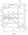
- FIGS. 1 and 2are cross-sectional views taken along substantially perpendicular planes of a multi-layer memory array 100 according to an embodiment of the present invention.
- Memory array 100can be a flash memory array, read only memory (ROM) array, a static random access memory (SRAM) array, a silicon-oxide-nitride-oxide-silicon (SONOS) memory array, or the like.
- ROMread only memory
- SRAMstatic random access memory
- SONOSsilicon-oxide-nitride-oxide-silicon
- Memory array 100includes a substrate 102 of silicon or the like.
- Layers 104 1 to 104 N of a memory materialare respectively formed at different levels within memory array. Specifically, layers 104 are formed (or stacked) one above the other on substrate 102 .
- a memory materialis any material whose properties can be electrically modified and read to determine whether the properties were modified. Moreover, for some memory materials, the electrically modified properties can be electrically restored to their original sate. Examples of memory materials include silicon, polysilicon, ferroelectric polymers, thin film transistors, etc.
- a dielectric layer 106such as an oxide layer or the like, is formed between successive layers 104 of memory material, separating them from each other.
- dielectric layers 106are a bulk dielectric layers, e.g., of a doped silicate glass, such as BSG (borosilicate glass), PSG (phosphosilicate glass), and BPSG (borophosphosilicate glass).
- BSGborosilicate glass
- PSGphosphosilicate glass
- BPSGborophosphosilicate glass
- a dielectric layer 106is formed on substrate 102 and a lowermost layer 104 , e.g., layer 104 1 , is formed on that dielectric layer 106 .
- the next dielectric layer 106is formed on the layer 104 1 , and the next layer of memory material, e.g., layer 104 2 , is formed on that dielectric layer 106 and so on.
- Each layer 104is patterned, etched, and processed, e.g., using standard processing, to produce intersecting column lines 108 and row (or word) lines 110 . Dashed lines in FIGS. 1 and 2 show the intersections.
- Memory array 100further includes a conductive layer (or global bit line) 112 and a conductive layer (or global row line) 114 , each formed overlying an uppermost layer 104 , e.g., layer 104 N , as shown in FIGS. 1 and 2 .
- an electrical contact 116electrically contacts each of the layers 104 to electrically interconnect them, as shown in FIG. 1 .
- electrical contact 116is an electrically conductive plug that is formed by etching the dielectric layers 106 and layers 104 so that contact 116 penetrates through each of the layers 104 .
- a suitable conductive plugincludes a nitride layer, such as titanium nitride (TiN), a first metal layer, such as titanium (Ti), on the nitride layer, and a second metal layer, such as tungsten (W), on the first metal layer.
- a contact 116passes through and electrically connects corresponding column lines 108 of the respective layers 104 .
- Contact 116is formed in a first plane containing the column lines 108 that contact 116 passes through, e.g., the plane of FIG. 1 .
- the first planeis substantially perpendicular to a second plane containing row lines 110 , e.g., the plane of FIG. 2 .
- contact 116is electrically connected to a source/drain region 118 of a select transistor (or gate) 120 , such as a field effect transistor (FET), that is formed on substrate 102 .
- a select transistoror gate
- FETfield effect transistor
- An electrically conductive plug 122electrically interconnects a source/drain region 124 of select transistor 120 and global bit line 112 in the first plane by passing through the dielectric layers 106 that form a single dielectric layer distally of ends of the layers 104 , as shown in FIG. 1 .
- a suitable conductive plug 122includes a nitride layer, such as titanium nitride (TiN), a first metal layer, such as titanium (Ti), on the nitride layer, and a second metal layer, such as tungsten (W), on the first metal layer. Therefore, each of the column lines 108 is electrically connected to global bit line 112 via select transistor 120 and conductive plug 122 .
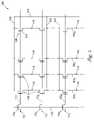
- an electrical contact 130located in the second plane, electrically contacts each of the layers 104 to electrically interconnect them in the second plane, as shown in FIG. 2 .
- the second planecontains the column lines 110 that contact 130 passes through.
- electrical contact 130is an electrically conductive plug that is formed by etching the dielectric layers 106 and layers 104 so that contact 130 penetrates through each of the layers 104 .
- a contact 130passes through and electrically connects corresponding row lines 110 of the respective layers 104 .
- contact 130is electrically connected to a source/drain region 132 of a select transistor (or gate) 134 , such as a field effect transistor (FET), that is formed on substrate 102 .
- FETfield effect transistor
- An electrically conductive plug 136electrically interconnects a source/drain region 138 of select transistor 134 and global row line 114 in the second plane by passing through the dielectric layers 106 that form a single dielectric layer distally of ends of the layers 104 , as shown in FIG. 2 . Therefore, each of the row lines 110 is electrically connected to global row line 114 via select transistor 134 and conductive plug 136 .
- a memory cell 150such as a non-volatile (or flash memory) cell, an SRAM cell, a ROM cell, etc., is located at each intersection of a column line 108 and a row line 110 , as shown in FIGS. 1 and 2 for the intersection of column line 108 2 and row line 110 2 of layer 104 2 .
- each row line 110contains a row of memory cells 150 and each column line 108 contains a column of memory cells 150 and thus each layer 104 contains an array of memory cells 150 .
- each memory cell 150is a floating gate transistor formed on the layer 104 , e.g., layer 104 2 , using silicon-on-sapphire (SOS) technology to form an SOS floating gate transistor, silicon-on-insulator (SOI) technology to form an SOI floating gate transistor, thin film transistor (TFT) technology to form a TFT floating gate transistor, thermoelectric polymer technology to form a thermoelectric polymer floating gate transistor, silicon-oxide-nitride-oxide-silicon (SONOS) technology to form a SONOS floating gate transistor, or the like.
- SOSsilicon-on-sapphire
- SOIsilicon-on-insulator
- TFTthin film transistor
- thermoelectric polymer technologyto form a thermoelectric polymer floating gate transistor
- SONOSsilicon-oxide-nitride-oxide-silicon
- the floating gate transistors 150include a source 152 and a drain 154 (shown in FIG. 1 ) constructed from an N + -type material of high impurity concentration formed in the layer 104 , a P-type semiconductor substrate, e.g., ploysilicon, of low impurity concentration.
- a tunneling dielectric 156e.g., a silicon oxide, is formed on the layer 104 at the intersection of the column line 108 and row line 110 , as shown in FIGS. 1 and 2 .
- a floating gate 158e.g., of polysilicon
- an interlayer dielectric 160e.g., of silicon oxide, nitride, or oxynitride, is formed on floating gate 158 , as shown in FIGS. 1 and 2 .
- a control gate 162e.g., of polysilicon, is formed on interlayer dielectric 160 in electrical contact with the corresponding row line 110 , e.g., row line 110 2 , as shown in FIG. 2 .
- Sidewall dielectric spacers 164are interposed between a portion of control gate 162 and floating gate 158 for further isolating control gate 162 from floating gate 158 , as shown in FIG. 2 .
- a select transistor (or gate) 170such as a field effect transistor (FET), is formed on each row line 110 between the memory cells 150 of that row line 110 and the electrical contact 130 , as illustrated in FIG. 2 for row line 110 2 .
- Select transistors 170enable one row line to be selected at a time, while one of the column lines 108 from each layer 104 is selected. For example, one row line 110 in the second plane is selected, while all of the column lines in the first plane are selected simultaneously. This enables the selection of a single memory cell 150 .
- selection of the memory cell 150 at the intersection of column line 108 2 and row line 110 2 of layer 104 2is accomplished by selecting all of column lines 108 in the first plane simultaneously (i.e., one column line 108 from each layer 104 ), e.g., by activating select transistor 134 , and selecting row line 110 2 in the second plane by activating the select transistor 170 formed on row line 110 2 .
- contact 130is connected directly to global row line 114 , thereby eliminating the need for select transistor 134 and conductive plug 136 when using select transistors 170 .
- a select transistor 170can be formed on each column line 108 between the memory cells 150 of that column line 108 and the electrical contact 116 instead of forming a select transistor 170 on each row line 110 .
- selection of the memory cell 150 at the intersection of column line 108 2 and row line 110 2 of layer 104 2is accomplished by selecting one row line 110 from each of layers 104 and selecting column line 108 2 using the select transistor 170 formed on column line 108 2 .
- contact 116is connected directly to global bit line 112 , thereby eliminating the need for select transistor 120 and conductive plug 122 when using select transistors 170 .
- FIG. 3is a cross-sectional view illustrating row line connections according to another embodiment of the present invention.
- FIG. 3shows an electrical contact 330 1 penetrating through a single row line 110 , e.g., row line 110 1 , and electrically connected thereto so as to electrically interconnect row line 110 1 and a source/drain region 332 1 of a select transistor 334 1 .
- Another electrical contact 330 2penetrates through another single row line 110 , e.g., row line 110 2 , and is electrically connected thereto so as to electrically interconnect row line 110 2 and a source/drain region 332 2 of a select transistor 334 2 .
- electrical contact 116penetrates through each of the column lines 108 , e.g., column lines 108 1 and 108 2 , as shown in FIG. 1 , and thus interconnects all of the column lines 108 .
- electrical contacts 330are as described for electrical contact 130
- select transistors 334are as described for select transistor 134 .
- a conductive plug 336 1electrically interconnects a source/drain region 138 1 of select transistor 334 1 and the global row line 114 . Therefore, row line 110 1 is electrically connected to global row line 114 via select transistor 334 1 and conductive plug 336 1 .
- Another conductive plug 336 2electrically interconnects a source/drain region 138 2 of select transistor 334 2 and the global row line 114 . Therefore, row line 110 2 is electrically connected to global row line 114 via select transistor 334 2 and conductive plug 336 2 .
- conductive plugs 336are as described for conductive plug 136 .
- a select transistorcan be formed on row lines 110 1 and 110 2 between the memory cells thereon and the respective contacts 336 1 and 336 2 , enabling contacts 336 to be connected directly to global row line 114 , thereby eliminating the need for select transistors 334 and conductive plugs 336 .
- Using a separate contact 330 for each of row lines 110 1 and 110 2enables individual selection of row line 110 1 or 110 2 , e.g., using the respective select transistor 334 . This enables the selection of a single memory cell 150 when one column line 108 is selected from each layer 104 .
- using a separate contact for each of column lines 108 1 and 108 2enables individual selection of column line 108 1 or 108 2 .
- Thisenables the selection of a single memory cell 150 when one of the row lines from each layer 104 , e.g., one row line 110 1 from layer 104 1 and one row line 110 2 from layer 104 2 , is interconnected by a single contact and is thus selected.
- each layer 104contains a NAND memory array 400 , as shown in FIG. 4 according to another embodiment of the present invention.
- Memory array 400includes row (or word) lines 404 1 to 404 P and intersecting column lines 402 1 to 402 M .
- Memory array 400includes NAND strings 406 1 to 406 M .
- Each NAND stringincludes floating gate transistors 408 1 to 408 P , each located at an intersection of a row line 402 and a column line 404 .
- the floating gate transistors 408represent non-volatile memory cells for storage of data.
- the floating gate transistors 408 of each NAND string 406are connected in series source to drain between a source select gate (or select transistor) 410 , e.g., an FET, and a drain select gate (or select transistor) 412 , e.g., an FET.
- a source select gate (or select transistor) 410e.g., an FET
- a drain select gate (or select transistor) 412e.g., an FET.
- Each source select gate 410is located at an intersection of a column line 404 and a source select line 414
- each drain select gate 412is located at an intersection of a column line 404 and a drain select line 415 .
- each drain select gate 412is connected to a contact 116 for the corresponding NAND string, and in this respect, contact 116 is a bit line contact.
- Contact 116is perpendicular to the plane of FIG. 4 and, for some embodiments, interconnects a drain region of a corresponding drain select gate 412 of each of the layers 104 to each other.
- the drain of a drain select gate 412 1 in each layer 104is connected to the contact 116 1 for the corresponding NAND string 406 1 of each layer 104 .
- the source of each drain select gate 412is connected to the drain of the last floating gate transistor 408 P of the corresponding NAND string 406 .
- drain select gate 412 1is connected to the drain of floating gate transistor 408 P of the corresponding NAND string 406 1 .
- Connecting column lines 402 to contacts 116 via drain select gates 412enables contact 116 to be connected directly to global bit line 112 , thereby eliminating the need for the select transistor 120 and the conductive plug 122 of FIG. 1 .
- a source of each source select gate 410is connected to a common source line 416 .
- a source line contact 418that is perpendicular to the plane of FIG. 4 interconnects a common source line 416 of each of the layers 104 to each other.
- source contact 418passes through each of the layers 104 , as is shown for contact 116 in FIG. 1 , and can be formed as a conductive plug as described above for contact 116 .
- the drain of each source select gate 410is connected to the source of the first floating gate transistor 408 of the corresponding NAND string 406 .
- the drain of source select gate 410 1is connected to the source of floating gate transistor 408 1 of the corresponding NAND string 406 1 .
- a control gate 420 of each source select gate 410is connected to source select line 414 .
- a contact 130is connected to each of row lines 404 , and a select transistor 170 is connected between each contact 130 and a first of the floating gate transistors 408 of each row line 404 .
- Contact 130is perpendicular to the plane of FIG. 4 and, for some embodiments, interconnects corresponding row lines of each of the layers 104 .
- a row line 404 1 in each layer 104is connected to the contact 130 1 .
- contact 130is a word line contact.
- a control line 430interconnects select transistors 170 , as shown in FIG. 4 , for activating select transistors 170 substantially simultaneously.
- Floating gate transistors 408have their control gates 436 coupled to a row (or word) line 404 that is connected to a given word line contact 130 .
- a column of the floating gate transistors 408is a NAND string 406 connected to a given bit line contact 116 .
- each layer 104contains a NOR memory array 500 , as shown in FIG. 5 according to another embodiment of the present invention.
- memory array 500includes row (or word) lines 502 1 to 502 N and intersecting column lines 504 1 to 504 Q .
- Floating gate transistors 506are located at each intersection of a row line 502 and a column line 504 .
- floating gate transistors 506represent non-volatile memory cells for storage of data.
- an adjacent pair of floating gate transistors 506has a common drain region therebetween that is connected to a contact (or bit-line contact) 116 , as shown in FIG. 5 .
- Contact 116is perpendicular to the plane of FIG. 5 and, for some embodiments, interconnects a corresponding common drain region of each of the layers 104 to each other.
- a column of the floating gate transistors 506are those transistors located on a given column line 504 .
- a row of the floating gate transistors 506are those transistors commonly connected to a given word line 502 .
- a contact 130is connected to each of the row lines 502 , and a select transistor 170 is connected between each contact 130 and a first of the floating gate transistors 506 of each row line 502 .
- Contact 130is perpendicular to the plane of FIG. 5 and, for some embodiments, interconnects corresponding row lines of each of the layers 104 .
- a row line 502 1 in each layer 104is connected to the contact 130 1 .
- Floating gate transistors 506have their control gates 514 coupled to a row (or word) line 502 that is connected to a given word line contact 130 .
- a control line 530interconnects select transistors 170 , as shown in FIG. 5 , for activating select transistors 170 substantially simultaneously.
- floating gate transistors 506 connected to two adjacent row lines 502may share the same array source 516 .
- array sources 516are regularly connected to a metal or other highly conductive line to provide a low-resistance path to ground.
- the array ground 518serves as this low-resistance path.
- FIG. 6is a simplified block diagram of a memory system 600 according to another embodiment of the present invention.
- Memory system 600includes an integrated circuit memory device 602 that includes an array 604 of memory cells, an address decoder 606 , row access circuitry 608 , column access circuitry 610 , control circuitry 612 , Input/Output (I/O) circuitry 614 , and an address buffer 616 .
- Memory system 600includes an external microprocessor 620 , or memory controller, electrically connected to memory device 602 for memory accessing as part of an electronic system.
- the memory device 602receives control signals from the processor 620 over a control link 622 .
- the memory cellsare used to store data that are accessed via a data (DQ) link 624 .
- DQdata
- Address signalsare received via an address link 626 that are decoded at address decoder 606 to access the memory array 604 .
- Address buffer circuit 616latches the address signals.
- the memory cellsare accessed in response to the control signals and the address signals. It will be appreciated by those skilled in the art that additional circuitry and control signals can be provided, and that the memory device of FIG. 6 has been simplified to help focus on the invention.
- the array of memory cells 604is formed in accordance with the present invention.
Landscapes
- Engineering & Computer Science (AREA)
- Microelectronics & Electronic Packaging (AREA)
- Semiconductor Memories (AREA)
- Non-Volatile Memory (AREA)
Abstract
Description
Claims (38)
Priority Applications (5)
| Application Number | Priority Date | Filing Date | Title |
|---|---|---|---|
| US10/786,765US7112815B2 (en) | 2004-02-25 | 2004-02-25 | Multi-layer memory arrays |
| PCT/US2005/005779WO2005083715A1 (en) | 2004-02-25 | 2005-02-24 | Multi-layer memory arrays |
| TW094105567ATWI262590B (en) | 2004-02-25 | 2005-02-24 | Multi-layer memory arrays |
| US11/392,290US7157305B2 (en) | 2004-02-25 | 2006-03-29 | Forming multi-layer memory arrays |
| US11/392,343US20060163614A1 (en) | 2004-02-25 | 2006-03-29 | Multi-layer memory arrays |
Applications Claiming Priority (1)
| Application Number | Priority Date | Filing Date | Title |
|---|---|---|---|
| US10/786,765US7112815B2 (en) | 2004-02-25 | 2004-02-25 | Multi-layer memory arrays |
Related Child Applications (2)
| Application Number | Title | Priority Date | Filing Date |
|---|---|---|---|
| US11/392,290DivisionUS7157305B2 (en) | 2004-02-25 | 2006-03-29 | Forming multi-layer memory arrays |
| US11/392,343DivisionUS20060163614A1 (en) | 2004-02-25 | 2006-03-29 | Multi-layer memory arrays |
Publications (2)
| Publication Number | Publication Date |
|---|---|
| US20050184329A1 US20050184329A1 (en) | 2005-08-25 |
| US7112815B2true US7112815B2 (en) | 2006-09-26 |
Family
ID=34861830
Family Applications (3)
| Application Number | Title | Priority Date | Filing Date |
|---|---|---|---|
| US10/786,765Expired - LifetimeUS7112815B2 (en) | 2004-02-25 | 2004-02-25 | Multi-layer memory arrays |
| US11/392,290Expired - LifetimeUS7157305B2 (en) | 2004-02-25 | 2006-03-29 | Forming multi-layer memory arrays |
| US11/392,343AbandonedUS20060163614A1 (en) | 2004-02-25 | 2006-03-29 | Multi-layer memory arrays |
Family Applications After (2)
| Application Number | Title | Priority Date | Filing Date |
|---|---|---|---|
| US11/392,290Expired - LifetimeUS7157305B2 (en) | 2004-02-25 | 2006-03-29 | Forming multi-layer memory arrays |
| US11/392,343AbandonedUS20060163614A1 (en) | 2004-02-25 | 2006-03-29 | Multi-layer memory arrays |
Country Status (3)
| Country | Link |
|---|---|
| US (3) | US7112815B2 (en) |
| TW (1) | TWI262590B (en) |
| WO (1) | WO2005083715A1 (en) |
Cited By (193)
| Publication number | Priority date | Publication date | Assignee | Title |
|---|---|---|---|---|
| US20060108627A1 (en)* | 2004-11-24 | 2006-05-25 | Samsung Electronics Co., Ltd. | NAND flash memory devices including multi-layer memory cell transistor structures and methods of fabricating the same |
| US20070132082A1 (en)* | 2005-12-12 | 2007-06-14 | Intel Corporation | Copper plating connection for multi-die stack in substrate package |
| US20070158731A1 (en)* | 2006-01-06 | 2007-07-12 | Samsung Electronics Co., Ltd. | Memory Devices Employing Ferroelectric Layer as Information Storage Elements and Methods of Fabricating the Same |
| KR100798816B1 (en) | 2006-10-10 | 2008-01-28 | 삼성전자주식회사 | NAND type nonvolatile memory device and method of forming the same |
| US20080023747A1 (en)* | 2006-07-25 | 2008-01-31 | Samsung Electronics Co., Ltd. | Semiconductor memory device with memory cells on multiple layers |
| US20080067554A1 (en)* | 2006-09-14 | 2008-03-20 | Jae-Hun Jeong | NAND flash memory device with 3-dimensionally arranged memory cell transistors |
| US7510954B1 (en)* | 2005-05-13 | 2009-03-31 | Micron Technology, Inc. | Memory array with surrounding gate access transistors and capacitors with global and staggered local bit lines |
| US7525141B1 (en) | 2005-05-13 | 2009-04-28 | Micron Technology, Inc. | Memory array with ultra-thin etched pillar surround gate access transistors and buried data/bit lines |
| US7566620B2 (en) | 2005-07-25 | 2009-07-28 | Micron Technology, Inc. | DRAM including a vertical surround gate transistor |
| US7601595B2 (en) | 2005-07-06 | 2009-10-13 | Micron Technology, Inc. | Surround gate access transistors with grown ultra-thin bodies |
| US7696567B2 (en) | 2005-08-31 | 2010-04-13 | Micron Technology, Inc | Semiconductor memory device |
| US20100271862A1 (en)* | 2009-04-23 | 2010-10-28 | Yoon Hongsik | Nonvolatile memory device |
| US20110076810A1 (en)* | 2009-09-25 | 2011-03-31 | Hewlett-Packard Development Company, L.P. | Three Dimensional Multilayer Circuit |
| US7982504B1 (en) | 2010-01-29 | 2011-07-19 | Hewlett Packard Development Company, L.P. | Interconnection architecture for multilayer circuits |
| US20110278527A1 (en)* | 2010-05-17 | 2011-11-17 | Yutaka Ishibashi | Semiconductor device |
| US20120211722A1 (en)* | 2009-11-06 | 2012-08-23 | Kellam Mark D | Three-dimensional memory array stacking structure |
| US20120280282A1 (en)* | 2010-01-29 | 2012-11-08 | Wei Wu | Three Dimensional Multilayer Circuit |
| US8373440B2 (en) | 2009-04-06 | 2013-02-12 | Hewlett-Packard Development Company, L.P. | Three dimensional multilayer circuit |
| US20130100743A1 (en)* | 2011-05-02 | 2013-04-25 | Macronix International Co., Ltd. | Method for operating a semiconductor structure |
| US8446767B2 (en) | 2010-07-02 | 2013-05-21 | Micron Technology, Inc. | Memories and their formation |
| US8735902B2 (en) | 2010-05-10 | 2014-05-27 | Micron Technology, Inc. | Memories with memory arrays extending in opposite directions from a semiconductor and their formation |
| US8873271B2 (en) | 2011-08-14 | 2014-10-28 | International Business Machines Corporation | 3D architecture for bipolar memory using bipolar access device |
| US8885422B2 (en) | 2009-06-12 | 2014-11-11 | Hewlett-Packard Development Company, L.P. | Hierarchical on-chip memory |
| US20170092541A1 (en)* | 2009-10-12 | 2017-03-30 | Monolithic 3D Inc. | 3d semiconductor device and structure |
| US10043781B2 (en) | 2009-10-12 | 2018-08-07 | Monolithic 3D Inc. | 3D semiconductor device and structure |
| US10115663B2 (en) | 2012-12-29 | 2018-10-30 | Monolithic 3D Inc. | 3D semiconductor device and structure |
| US10127344B2 (en) | 2013-04-15 | 2018-11-13 | Monolithic 3D Inc. | Automation for monolithic 3D devices |
| US10157909B2 (en) | 2009-10-12 | 2018-12-18 | Monolithic 3D Inc. | 3D semiconductor device and structure |
| US10217667B2 (en) | 2011-06-28 | 2019-02-26 | Monolithic 3D Inc. | 3D semiconductor device, fabrication method and system |
| US10224279B2 (en) | 2013-03-15 | 2019-03-05 | Monolithic 3D Inc. | Semiconductor device and structure |
| US10290682B2 (en) | 2010-10-11 | 2019-05-14 | Monolithic 3D Inc. | 3D IC semiconductor device and structure with stacked memory |
| US10297586B2 (en) | 2015-03-09 | 2019-05-21 | Monolithic 3D Inc. | Methods for processing a 3D semiconductor device |
| US10325651B2 (en) | 2013-03-11 | 2019-06-18 | Monolithic 3D Inc. | 3D semiconductor device with stacked memory |
| US10354995B2 (en) | 2009-10-12 | 2019-07-16 | Monolithic 3D Inc. | Semiconductor memory device and structure |
| US10355121B2 (en) | 2013-03-11 | 2019-07-16 | Monolithic 3D Inc. | 3D semiconductor device with stacked memory |
| US10366970B2 (en) | 2009-10-12 | 2019-07-30 | Monolithic 3D Inc. | 3D semiconductor device and structure |
| US10381328B2 (en) | 2015-04-19 | 2019-08-13 | Monolithic 3D Inc. | Semiconductor device and structure |
| US10388568B2 (en) | 2011-06-28 | 2019-08-20 | Monolithic 3D Inc. | 3D semiconductor device and system |
| US10388863B2 (en) | 2009-10-12 | 2019-08-20 | Monolithic 3D Inc. | 3D memory device and structure |
| US10418369B2 (en) | 2015-10-24 | 2019-09-17 | Monolithic 3D Inc. | Multi-level semiconductor memory device and structure |
| US10497713B2 (en) | 2010-11-18 | 2019-12-03 | Monolithic 3D Inc. | 3D semiconductor memory device and structure |
| US10515981B2 (en) | 2015-09-21 | 2019-12-24 | Monolithic 3D Inc. | Multilevel semiconductor device and structure with memory |
| US10522225B1 (en) | 2015-10-02 | 2019-12-31 | Monolithic 3D Inc. | Semiconductor device with non-volatile memory |
| US10600657B2 (en) | 2012-12-29 | 2020-03-24 | Monolithic 3D Inc | 3D semiconductor device and structure |
| US10600888B2 (en) | 2012-04-09 | 2020-03-24 | Monolithic 3D Inc. | 3D semiconductor device |
| US10651054B2 (en) | 2012-12-29 | 2020-05-12 | Monolithic 3D Inc. | 3D semiconductor device and structure |
| US10679977B2 (en) | 2010-10-13 | 2020-06-09 | Monolithic 3D Inc. | 3D microdisplay device and structure |
| US10825779B2 (en) | 2015-04-19 | 2020-11-03 | Monolithic 3D Inc. | 3D semiconductor device and structure |
| US10833108B2 (en) | 2010-10-13 | 2020-11-10 | Monolithic 3D Inc. | 3D microdisplay device and structure |
| US10840239B2 (en) | 2014-08-26 | 2020-11-17 | Monolithic 3D Inc. | 3D semiconductor device and structure |
| US10847540B2 (en) | 2015-10-24 | 2020-11-24 | Monolithic 3D Inc. | 3D semiconductor memory device and structure |
| US10892016B1 (en) | 2019-04-08 | 2021-01-12 | Monolithic 3D Inc. | 3D memory semiconductor devices and structures |
| US10892169B2 (en) | 2012-12-29 | 2021-01-12 | Monolithic 3D Inc. | 3D semiconductor device and structure |
| US10896931B1 (en) | 2010-10-11 | 2021-01-19 | Monolithic 3D Inc. | 3D semiconductor device and structure |
| US10903089B1 (en) | 2012-12-29 | 2021-01-26 | Monolithic 3D Inc. | 3D semiconductor device and structure |
| US10910364B2 (en) | 2009-10-12 | 2021-02-02 | Monolitaic 3D Inc. | 3D semiconductor device |
| US10943934B2 (en) | 2010-10-13 | 2021-03-09 | Monolithic 3D Inc. | Multilevel semiconductor device and structure |
| US10978501B1 (en) | 2010-10-13 | 2021-04-13 | Monolithic 3D Inc. | Multilevel semiconductor device and structure with waveguides |
| US10998374B1 (en) | 2010-10-13 | 2021-05-04 | Monolithic 3D Inc. | Multilevel semiconductor device and structure |
| US11004719B1 (en) | 2010-11-18 | 2021-05-11 | Monolithic 3D Inc. | Methods for producing a 3D semiconductor memory device and structure |
| US11004694B1 (en) | 2012-12-29 | 2021-05-11 | Monolithic 3D Inc. | 3D semiconductor device and structure |
| US11011507B1 (en) | 2015-04-19 | 2021-05-18 | Monolithic 3D Inc. | 3D semiconductor device and structure |
| US11018191B1 (en) | 2010-10-11 | 2021-05-25 | Monolithic 3D Inc. | 3D semiconductor device and structure |
| US11018116B2 (en) | 2012-12-22 | 2021-05-25 | Monolithic 3D Inc. | Method to form a 3D semiconductor device and structure |
| US11018133B2 (en) | 2009-10-12 | 2021-05-25 | Monolithic 3D Inc. | 3D integrated circuit |
| US11018156B2 (en) | 2019-04-08 | 2021-05-25 | Monolithic 3D Inc. | 3D memory semiconductor devices and structures |
| US11018042B1 (en) | 2010-11-18 | 2021-05-25 | Monolithic 3D Inc. | 3D semiconductor memory device and structure |
| US11024673B1 (en) | 2010-10-11 | 2021-06-01 | Monolithic 3D Inc. | 3D semiconductor device and structure |
| US11030371B2 (en) | 2013-04-15 | 2021-06-08 | Monolithic 3D Inc. | Automation for monolithic 3D devices |
| US11031275B2 (en) | 2010-11-18 | 2021-06-08 | Monolithic 3D Inc. | 3D semiconductor device and structure with memory |
| US11031394B1 (en) | 2014-01-28 | 2021-06-08 | Monolithic 3D Inc. | 3D semiconductor device and structure |
| US11043523B1 (en) | 2010-10-13 | 2021-06-22 | Monolithic 3D Inc. | Multilevel semiconductor device and structure with image sensors |
| US11056468B1 (en) | 2015-04-19 | 2021-07-06 | Monolithic 3D Inc. | 3D semiconductor device and structure |
| US11063071B1 (en) | 2010-10-13 | 2021-07-13 | Monolithic 3D Inc. | Multilevel semiconductor device and structure with waveguides |
| US11063024B1 (en) | 2012-12-22 | 2021-07-13 | Monlithic 3D Inc. | Method to form a 3D semiconductor device and structure |
| US11087995B1 (en) | 2012-12-29 | 2021-08-10 | Monolithic 3D Inc. | 3D semiconductor device and structure |
| US11088130B2 (en) | 2014-01-28 | 2021-08-10 | Monolithic 3D Inc. | 3D semiconductor device and structure |
| US11088050B2 (en) | 2012-04-09 | 2021-08-10 | Monolithic 3D Inc. | 3D semiconductor device with isolation layers |
| US11094576B1 (en) | 2010-11-18 | 2021-08-17 | Monolithic 3D Inc. | Methods for producing a 3D semiconductor memory device and structure |
| US11107721B2 (en) | 2010-11-18 | 2021-08-31 | Monolithic 3D Inc. | 3D semiconductor device and structure with NAND logic |
| US11107808B1 (en) | 2014-01-28 | 2021-08-31 | Monolithic 3D Inc. | 3D semiconductor device and structure |
| US11114464B2 (en) | 2015-10-24 | 2021-09-07 | Monolithic 3D Inc. | 3D semiconductor device and structure |
| US11114427B2 (en) | 2015-11-07 | 2021-09-07 | Monolithic 3D Inc. | 3D semiconductor processor and memory device and structure |
| US11121021B2 (en) | 2010-11-18 | 2021-09-14 | Monolithic 3D Inc. | 3D semiconductor device and structure |
| US11133344B2 (en) | 2010-10-13 | 2021-09-28 | Monolithic 3D Inc. | Multilevel semiconductor device and structure with image sensors |
| US11158674B2 (en) | 2010-10-11 | 2021-10-26 | Monolithic 3D Inc. | Method to produce a 3D semiconductor device and structure |
| US11158652B1 (en) | 2019-04-08 | 2021-10-26 | Monolithic 3D Inc. | 3D memory semiconductor devices and structures |
| US11164811B2 (en) | 2012-04-09 | 2021-11-02 | Monolithic 3D Inc. | 3D semiconductor device with isolation layers and oxide-to-oxide bonding |
| US11163112B2 (en) | 2010-10-13 | 2021-11-02 | Monolithic 3D Inc. | Multilevel semiconductor device and structure with electromagnetic modulators |
| US11164770B1 (en) | 2010-11-18 | 2021-11-02 | Monolithic 3D Inc. | Method for producing a 3D semiconductor memory device and structure |
| US11164898B2 (en) | 2010-10-13 | 2021-11-02 | Monolithic 3D Inc. | Multilevel semiconductor device and structure |
| US11177140B2 (en) | 2012-12-29 | 2021-11-16 | Monolithic 3D Inc. | 3D semiconductor device and structure |
| US11211279B2 (en) | 2010-11-18 | 2021-12-28 | Monolithic 3D Inc. | Method for processing a 3D integrated circuit and structure |
| US11217565B2 (en) | 2012-12-22 | 2022-01-04 | Monolithic 3D Inc. | Method to form a 3D semiconductor device and structure |
| US11227897B2 (en) | 2010-10-11 | 2022-01-18 | Monolithic 3D Inc. | Method for producing a 3D semiconductor memory device and structure |
| US11251149B2 (en) | 2016-10-10 | 2022-02-15 | Monolithic 3D Inc. | 3D memory device and structure |
| US11257867B1 (en) | 2010-10-11 | 2022-02-22 | Monolithic 3D Inc. | 3D semiconductor device and structure with oxide bonds |
| US11270055B1 (en) | 2013-04-15 | 2022-03-08 | Monolithic 3D Inc. | Automation for monolithic 3D devices |
| US11296115B1 (en) | 2015-10-24 | 2022-04-05 | Monolithic 3D Inc. | 3D semiconductor device and structure |
| US11296106B2 (en) | 2019-04-08 | 2022-04-05 | Monolithic 3D Inc. | 3D memory semiconductor devices and structures |
| US11309292B2 (en) | 2012-12-22 | 2022-04-19 | Monolithic 3D Inc. | 3D semiconductor device and structure with metal layers |
| US11315980B1 (en) | 2010-10-11 | 2022-04-26 | Monolithic 3D Inc. | 3D semiconductor device and structure with transistors |
| US11329059B1 (en) | 2016-10-10 | 2022-05-10 | Monolithic 3D Inc. | 3D memory devices and structures with thinned single crystal substrates |
| US11327227B2 (en) | 2010-10-13 | 2022-05-10 | Monolithic 3D Inc. | Multilevel semiconductor device and structure with electromagnetic modulators |
| US11341309B1 (en) | 2013-04-15 | 2022-05-24 | Monolithic 3D Inc. | Automation for monolithic 3D devices |
| US11355381B2 (en) | 2010-11-18 | 2022-06-07 | Monolithic 3D Inc. | 3D semiconductor memory device and structure |
| US11355380B2 (en) | 2010-11-18 | 2022-06-07 | Monolithic 3D Inc. | Methods for producing 3D semiconductor memory device and structure utilizing alignment marks |
| US11374118B2 (en) | 2009-10-12 | 2022-06-28 | Monolithic 3D Inc. | Method to form a 3D integrated circuit |
| US11398569B2 (en) | 2013-03-12 | 2022-07-26 | Monolithic 3D Inc. | 3D semiconductor device and structure |
| US11404466B2 (en) | 2010-10-13 | 2022-08-02 | Monolithic 3D Inc. | Multilevel semiconductor device and structure with image sensors |
| US11410912B2 (en) | 2012-04-09 | 2022-08-09 | Monolithic 3D Inc. | 3D semiconductor device with vias and isolation layers |
| US11430668B2 (en) | 2012-12-29 | 2022-08-30 | Monolithic 3D Inc. | 3D semiconductor device and structure with bonding |
| US11430667B2 (en) | 2012-12-29 | 2022-08-30 | Monolithic 3D Inc. | 3D semiconductor device and structure with bonding |
| US11437368B2 (en) | 2010-10-13 | 2022-09-06 | Monolithic 3D Inc. | Multilevel semiconductor device and structure with oxide bonding |
| US11443971B2 (en) | 2010-11-18 | 2022-09-13 | Monolithic 3D Inc. | 3D semiconductor device and structure with memory |
| US11469271B2 (en) | 2010-10-11 | 2022-10-11 | Monolithic 3D Inc. | Method to produce 3D semiconductor devices and structures with memory |
| US11476181B1 (en) | 2012-04-09 | 2022-10-18 | Monolithic 3D Inc. | 3D semiconductor device and structure with metal layers |
| US11482439B2 (en) | 2010-11-18 | 2022-10-25 | Monolithic 3D Inc. | Methods for producing a 3D semiconductor memory device comprising charge trap junction-less transistors |
| US11482440B2 (en) | 2010-12-16 | 2022-10-25 | Monolithic 3D Inc. | 3D semiconductor device and structure with a built-in test circuit for repairing faulty circuits |
| US11482438B2 (en) | 2010-11-18 | 2022-10-25 | Monolithic 3D Inc. | Methods for producing a 3D semiconductor memory device and structure |
| US11487928B2 (en) | 2013-04-15 | 2022-11-01 | Monolithic 3D Inc. | Automation for monolithic 3D devices |
| US11495484B2 (en) | 2010-11-18 | 2022-11-08 | Monolithic 3D Inc. | 3D semiconductor devices and structures with at least two single-crystal layers |
| US11508605B2 (en) | 2010-11-18 | 2022-11-22 | Monolithic 3D Inc. | 3D semiconductor memory device and structure |
| US11521888B2 (en) | 2010-11-18 | 2022-12-06 | Monolithic 3D Inc. | 3D semiconductor device and structure with high-k metal gate transistors |
| US11569117B2 (en) | 2010-11-18 | 2023-01-31 | Monolithic 3D Inc. | 3D semiconductor device and structure with single-crystal layers |
| US11574109B1 (en) | 2013-04-15 | 2023-02-07 | Monolithic 3D Inc | Automation methods for 3D integrated circuits and devices |
| US11594473B2 (en) | 2012-04-09 | 2023-02-28 | Monolithic 3D Inc. | 3D semiconductor device and structure with metal layers and a connective path |
| US11600667B1 (en) | 2010-10-11 | 2023-03-07 | Monolithic 3D Inc. | Method to produce 3D semiconductor devices and structures with memory |
| US11605663B2 (en) | 2010-10-13 | 2023-03-14 | Monolithic 3D Inc. | Multilevel semiconductor device and structure with image sensors and wafer bonding |
| US11610802B2 (en) | 2010-11-18 | 2023-03-21 | Monolithic 3D Inc. | Method for producing a 3D semiconductor device and structure with single crystal transistors and metal gate electrodes |
| US11615977B2 (en) | 2010-11-18 | 2023-03-28 | Monolithic 3D Inc. | 3D semiconductor memory device and structure |
| US11616004B1 (en) | 2012-04-09 | 2023-03-28 | Monolithic 3D Inc. | 3D semiconductor device and structure with metal layers and a connective path |
| US11694922B2 (en) | 2010-10-13 | 2023-07-04 | Monolithic 3D Inc. | Multilevel semiconductor device and structure with oxide bonding |
| US11694944B1 (en) | 2012-04-09 | 2023-07-04 | Monolithic 3D Inc. | 3D semiconductor device and structure with metal layers and a connective path |
| US11711928B2 (en) | 2016-10-10 | 2023-07-25 | Monolithic 3D Inc. | 3D memory devices and structures with control circuits |
| US11720736B2 (en) | 2013-04-15 | 2023-08-08 | Monolithic 3D Inc. | Automation methods for 3D integrated circuits and devices |
| US11735462B2 (en) | 2010-11-18 | 2023-08-22 | Monolithic 3D Inc. | 3D semiconductor device and structure with single-crystal layers |
| US11735501B1 (en) | 2012-04-09 | 2023-08-22 | Monolithic 3D Inc. | 3D semiconductor device and structure with metal layers and a connective path |
| US11763864B2 (en) | 2019-04-08 | 2023-09-19 | Monolithic 3D Inc. | 3D memory semiconductor devices and structures with bit-line pillars |
| US11784082B2 (en) | 2010-11-18 | 2023-10-10 | Monolithic 3D Inc. | 3D semiconductor device and structure with bonding |
| US11784169B2 (en) | 2012-12-22 | 2023-10-10 | Monolithic 3D Inc. | 3D semiconductor device and structure with metal layers |
| US11804396B2 (en) | 2010-11-18 | 2023-10-31 | Monolithic 3D Inc. | Methods for producing a 3D semiconductor device and structure with memory cells and multiple metal layers |
| US11812620B2 (en) | 2016-10-10 | 2023-11-07 | Monolithic 3D Inc. | 3D DRAM memory devices and structures with control circuits |
| US11855114B2 (en) | 2010-10-13 | 2023-12-26 | Monolithic 3D Inc. | Multilevel semiconductor device and structure with image sensors and wafer bonding |
| US11854857B1 (en) | 2010-11-18 | 2023-12-26 | Monolithic 3D Inc. | Methods for producing a 3D semiconductor device and structure with memory cells and multiple metal layers |
| US11855100B2 (en) | 2010-10-13 | 2023-12-26 | Monolithic 3D Inc. | Multilevel semiconductor device and structure with oxide bonding |
| US11862503B2 (en) | 2010-11-18 | 2024-01-02 | Monolithic 3D Inc. | Method for producing a 3D semiconductor device and structure with memory cells and multiple metal layers |
| US11869915B2 (en) | 2010-10-13 | 2024-01-09 | Monolithic 3D Inc. | Multilevel semiconductor device and structure with image sensors and wafer bonding |
| US11869965B2 (en) | 2013-03-11 | 2024-01-09 | Monolithic 3D Inc. | 3D semiconductor device and structure with metal layers and memory cells |
| US11869591B2 (en) | 2016-10-10 | 2024-01-09 | Monolithic 3D Inc. | 3D memory devices and structures with control circuits |
| US11881443B2 (en) | 2012-04-09 | 2024-01-23 | Monolithic 3D Inc. | 3D semiconductor device and structure with metal layers and a connective path |
| US11901210B2 (en) | 2010-11-18 | 2024-02-13 | Monolithic 3D Inc. | 3D semiconductor device and structure with memory |
| US11916045B2 (en) | 2012-12-22 | 2024-02-27 | Monolithic 3D Inc. | 3D semiconductor device and structure with metal layers |
| US11923374B2 (en) | 2013-03-12 | 2024-03-05 | Monolithic 3D Inc. | 3D semiconductor device and structure with metal layers |
| US11923230B1 (en) | 2010-11-18 | 2024-03-05 | Monolithic 3D Inc. | 3D semiconductor device and structure with bonding |
| US11930648B1 (en) | 2016-10-10 | 2024-03-12 | Monolithic 3D Inc. | 3D memory devices and structures with metal layers |
| US11929372B2 (en) | 2010-10-13 | 2024-03-12 | Monolithic 3D Inc. | Multilevel semiconductor device and structure with image sensors and wafer bonding |
| US11937422B2 (en) | 2015-11-07 | 2024-03-19 | Monolithic 3D Inc. | Semiconductor memory device and structure |
| US11935949B1 (en) | 2013-03-11 | 2024-03-19 | Monolithic 3D Inc. | 3D semiconductor device and structure with metal layers and memory cells |
| US11956952B2 (en) | 2015-08-23 | 2024-04-09 | Monolithic 3D Inc. | Semiconductor memory device and structure |
| US11961827B1 (en) | 2012-12-22 | 2024-04-16 | Monolithic 3D Inc. | 3D semiconductor device and structure with metal layers |
| US11967583B2 (en) | 2012-12-22 | 2024-04-23 | Monolithic 3D Inc. | 3D semiconductor device and structure with metal layers |
| US11978731B2 (en) | 2015-09-21 | 2024-05-07 | Monolithic 3D Inc. | Method to produce a multi-level semiconductor memory device and structure |
| US11984445B2 (en) | 2009-10-12 | 2024-05-14 | Monolithic 3D Inc. | 3D semiconductor devices and structures with metal layers |
| US11984438B2 (en) | 2010-10-13 | 2024-05-14 | Monolithic 3D Inc. | Multilevel semiconductor device and structure with oxide bonding |
| US11991884B1 (en) | 2015-10-24 | 2024-05-21 | Monolithic 3D Inc. | 3D semiconductor device and structure with logic and memory |
| US12016181B2 (en) | 2015-10-24 | 2024-06-18 | Monolithic 3D Inc. | 3D semiconductor device and structure with logic and memory |
| US12027518B1 (en) | 2009-10-12 | 2024-07-02 | Monolithic 3D Inc. | 3D semiconductor devices and structures with metal layers |
| US12035531B2 (en) | 2015-10-24 | 2024-07-09 | Monolithic 3D Inc. | 3D semiconductor device and structure with logic and memory |
| US12033884B2 (en) | 2010-11-18 | 2024-07-09 | Monolithic 3D Inc. | Methods for producing a 3D semiconductor device and structure with memory cells and multiple metal layers |
| US12051674B2 (en) | 2012-12-22 | 2024-07-30 | Monolithic 3D Inc. | 3D semiconductor device and structure with metal layers |
| US12068187B2 (en) | 2010-11-18 | 2024-08-20 | Monolithic 3D Inc. | 3D semiconductor device and structure with bonding and DRAM memory cells |
| US12080743B2 (en) | 2010-10-13 | 2024-09-03 | Monolithic 3D Inc. | Multilevel semiconductor device and structure with image sensors and wafer bonding |
| US12094829B2 (en) | 2014-01-28 | 2024-09-17 | Monolithic 3D Inc. | 3D semiconductor device and structure |
| US12094965B2 (en) | 2013-03-11 | 2024-09-17 | Monolithic 3D Inc. | 3D semiconductor device and structure with metal layers and memory cells |
| US12094892B2 (en) | 2010-10-13 | 2024-09-17 | Monolithic 3D Inc. | 3D micro display device and structure |
| US12100646B2 (en) | 2013-03-12 | 2024-09-24 | Monolithic 3D Inc. | 3D semiconductor device and structure with metal layers |
| US12100658B2 (en) | 2015-09-21 | 2024-09-24 | Monolithic 3D Inc. | Method to produce a 3D multilayer semiconductor device and structure |
| US12100611B2 (en) | 2010-11-18 | 2024-09-24 | Monolithic 3D Inc. | Methods for producing a 3D semiconductor device and structure with memory cells and multiple metal layers |
| US12120880B1 (en) | 2015-10-24 | 2024-10-15 | Monolithic 3D Inc. | 3D semiconductor device and structure with logic and memory |
| US12125737B1 (en) | 2010-11-18 | 2024-10-22 | Monolithic 3D Inc. | 3D semiconductor device and structure with metal layers and memory cells |
| US12136562B2 (en) | 2010-11-18 | 2024-11-05 | Monolithic 3D Inc. | 3D semiconductor device and structure with single-crystal layers |
| US12144190B2 (en) | 2010-11-18 | 2024-11-12 | Monolithic 3D Inc. | 3D semiconductor device and structure with bonding and memory cells preliminary class |
| US12154817B1 (en) | 2010-11-18 | 2024-11-26 | Monolithic 3D Inc. | Methods for producing a 3D semiconductor memory device and structure |
| US12178055B2 (en) | 2015-09-21 | 2024-12-24 | Monolithic 3D Inc. | 3D semiconductor memory devices and structures |
| US12219769B2 (en) | 2015-10-24 | 2025-02-04 | Monolithic 3D Inc. | 3D semiconductor device and structure with logic and memory |
| US12225704B2 (en) | 2016-10-10 | 2025-02-11 | Monolithic 3D Inc. | 3D memory devices and structures with memory arrays and metal layers |
| US12243765B2 (en) | 2010-11-18 | 2025-03-04 | Monolithic 3D Inc. | 3D semiconductor device and structure with metal layers and memory cells |
| US12250830B2 (en) | 2015-09-21 | 2025-03-11 | Monolithic 3D Inc. | 3D semiconductor memory devices and structures |
| US12249538B2 (en) | 2012-12-29 | 2025-03-11 | Monolithic 3D Inc. | 3D semiconductor device and structure including power distribution grids |
| US12272586B2 (en) | 2010-11-18 | 2025-04-08 | Monolithic 3D Inc. | 3D semiconductor memory device and structure with memory and metal layers |
| US12362219B2 (en) | 2010-11-18 | 2025-07-15 | Monolithic 3D Inc. | 3D semiconductor memory device and structure |
| US12360310B2 (en) | 2010-10-13 | 2025-07-15 | Monolithic 3D Inc. | Multilevel semiconductor device and structure with oxide bonding |
Families Citing this family (19)
| Publication number | Priority date | Publication date | Assignee | Title |
|---|---|---|---|---|
| KR100746220B1 (en)* | 2004-01-12 | 2007-08-03 | 삼성전자주식회사 | Semiconductor integrated circuits employing stacked node contact structures and stacked thin film transistors and methods of fabricating the same |
| US8482052B2 (en)* | 2005-01-03 | 2013-07-09 | Macronix International Co., Ltd. | Silicon on insulator and thin film transistor bandgap engineered split gate memory |
| KR100607413B1 (en)* | 2005-04-27 | 2006-08-01 | 삼성전자주식회사 | Stacked semiconductor device and method of manufacturing the same |
| JP4822791B2 (en)* | 2005-10-04 | 2011-11-24 | ルネサスエレクトロニクス株式会社 | Semiconductor memory device |
| US7414280B2 (en)* | 2005-10-21 | 2008-08-19 | Macronix International Co., Ltd. | Systems and methods for memory structure comprising embedded flash memory |
| US7851851B2 (en)* | 2007-03-27 | 2010-12-14 | Sandisk 3D Llc | Three dimensional NAND memory |
| US7745265B2 (en)* | 2007-03-27 | 2010-06-29 | Sandisk 3D, Llc | Method of making three dimensional NAND memory |
| US7848145B2 (en)* | 2007-03-27 | 2010-12-07 | Sandisk 3D Llc | Three dimensional NAND memory |
| US7808038B2 (en) | 2007-03-27 | 2010-10-05 | Sandisk 3D Llc | Method of making three dimensional NAND memory |
| US8362615B2 (en)* | 2007-08-29 | 2013-01-29 | Macronix International Co., Ltd. | Memory and manufacturing method thereof |
| KR100944605B1 (en)* | 2007-12-24 | 2010-02-25 | 주식회사 동부하이텍 | Semiconductor device |
| US8902650B2 (en)* | 2012-08-30 | 2014-12-02 | Micron Technology, Inc. | Memory devices and operating methods for a memory device |
| TWI566328B (en)* | 2013-07-29 | 2017-01-11 | 高效電源轉換公司 | Gallium nitride transistor having a polysilicon layer for generating additional components |
| US20150262671A1 (en)* | 2014-03-13 | 2015-09-17 | Kabushiki Kaisha Toshiba | Non-volatile memory device |
| US10008265B2 (en) | 2014-09-06 | 2018-06-26 | NEO Semiconductor, Inc. | Method and apparatus for providing three-dimensional integrated nonvolatile memory (NVM) and dynamic random access memory (DRAM) memory device |
| TW201629955A (en)* | 2014-10-26 | 2016-08-16 | Neo半導體股份有限公司 | Method and apparatus for providing three-dimensional integrated nonvolatile memory and dynamic random access memory memory device |
| KR102291518B1 (en)* | 2015-03-20 | 2021-08-20 | 삼성전자주식회사 | Nonvolatile memory device and storage deice including nonvolatile memory device |
| CN107646137B (en)* | 2015-06-23 | 2022-03-08 | 英特尔公司 | Stackable thin film memory |
| US12255143B2 (en)* | 2021-02-26 | 2025-03-18 | Micron Technology, Inc. | Microelectronic devices including composite pad structures on staircase structures, and related methods, memory devices, and electronic systems |
Citations (16)
| Publication number | Priority date | Publication date | Assignee | Title |
|---|---|---|---|---|
| US5091762A (en) | 1988-07-05 | 1992-02-25 | Kabushiki Kaisha Toshiba | Semiconductor memory device with a 3-dimensional structure |
| US6034882A (en) | 1998-11-16 | 2000-03-07 | Matrix Semiconductor, Inc. | Vertically stacked field programmable nonvolatile memory and method of fabrication |
| US6377504B1 (en) | 2000-12-12 | 2002-04-23 | Tachuon Semiconductor Corp | High-density memory utilizing multiplexers to reduce bit line pitch constraints |
| US20020079520A1 (en) | 2000-05-26 | 2002-06-27 | Toshiyuki Nishihara | Ferroelectric-type nonvolatile semiconductor memory and operation method thereof |
| EP1308958A2 (en) | 2001-10-31 | 2003-05-07 | Hewlett-Packard Company | Three dimensional large storage random access memory device |
| EP1318522A2 (en) | 2001-12-10 | 2003-06-11 | Hewlett-Packard Company | Memory devices |
| US20030132458A1 (en) | 2002-01-16 | 2003-07-17 | Van Brocklin Andrew L. | Memory structure and method making |
| US6636442B2 (en)* | 2002-01-29 | 2003-10-21 | Lattice Semiconductor Corporation | Non-volatile memory element having a cascoded transistor scheme to reduce oxide field stress |
| US20030214835A1 (en) | 2002-05-16 | 2003-11-20 | Hasan Nejad | Stacked 1t-nmtj mram structure |
| US6657250B1 (en) | 2002-08-21 | 2003-12-02 | Micron Technology, Inc. | Vertical flash memory cell with buried source rail |
| US20030224535A1 (en) | 2002-05-31 | 2003-12-04 | Ebrahim Andideh | Forming ferroelectric polymer memories |
| US20040003191A1 (en) | 2002-06-28 | 2004-01-01 | Minne Mark W. | Write-once memory storage device |
| US20040026730A1 (en) | 2002-08-08 | 2004-02-12 | Kostylev Sergey A. | Programmable resistance memory element with layered memory material |
| US6735104B2 (en) | 2001-03-21 | 2004-05-11 | Matrix Semiconductor, Inc. | Memory device with row and column decoder circuits arranged in a checkerboard pattern under a plurality of memory arrays |
| US6822903B2 (en) | 2003-03-31 | 2004-11-23 | Matrix Semiconductor, Inc. | Apparatus and method for disturb-free programming of passive element memory cells |
| US6937248B2 (en)* | 2001-07-26 | 2005-08-30 | Koninklijke Philips Electronics N.V. | Pixel array with indirectly associated memory |
Family Cites Families (1)
| Publication number | Priority date | Publication date | Assignee | Title |
|---|---|---|---|---|
| US7009235B2 (en)* | 2003-11-10 | 2006-03-07 | Unity Semiconductor Corporation | Conductive memory stack with non-uniform width |
- 2004
- 2004-02-25USUS10/786,765patent/US7112815B2/ennot_activeExpired - Lifetime
- 2005
- 2005-02-24TWTW094105567Apatent/TWI262590B/ennot_activeIP Right Cessation
- 2005-02-24WOPCT/US2005/005779patent/WO2005083715A1/enactiveApplication Filing
- 2006
- 2006-03-29USUS11/392,290patent/US7157305B2/ennot_activeExpired - Lifetime
- 2006-03-29USUS11/392,343patent/US20060163614A1/ennot_activeAbandoned
Patent Citations (16)
| Publication number | Priority date | Publication date | Assignee | Title |
|---|---|---|---|---|
| US5091762A (en) | 1988-07-05 | 1992-02-25 | Kabushiki Kaisha Toshiba | Semiconductor memory device with a 3-dimensional structure |
| US6034882A (en) | 1998-11-16 | 2000-03-07 | Matrix Semiconductor, Inc. | Vertically stacked field programmable nonvolatile memory and method of fabrication |
| US20020079520A1 (en) | 2000-05-26 | 2002-06-27 | Toshiyuki Nishihara | Ferroelectric-type nonvolatile semiconductor memory and operation method thereof |
| US6377504B1 (en) | 2000-12-12 | 2002-04-23 | Tachuon Semiconductor Corp | High-density memory utilizing multiplexers to reduce bit line pitch constraints |
| US6735104B2 (en) | 2001-03-21 | 2004-05-11 | Matrix Semiconductor, Inc. | Memory device with row and column decoder circuits arranged in a checkerboard pattern under a plurality of memory arrays |
| US6937248B2 (en)* | 2001-07-26 | 2005-08-30 | Koninklijke Philips Electronics N.V. | Pixel array with indirectly associated memory |
| EP1308958A2 (en) | 2001-10-31 | 2003-05-07 | Hewlett-Packard Company | Three dimensional large storage random access memory device |
| EP1318522A2 (en) | 2001-12-10 | 2003-06-11 | Hewlett-Packard Company | Memory devices |
| US20030132458A1 (en) | 2002-01-16 | 2003-07-17 | Van Brocklin Andrew L. | Memory structure and method making |
| US6636442B2 (en)* | 2002-01-29 | 2003-10-21 | Lattice Semiconductor Corporation | Non-volatile memory element having a cascoded transistor scheme to reduce oxide field stress |
| US20030214835A1 (en) | 2002-05-16 | 2003-11-20 | Hasan Nejad | Stacked 1t-nmtj mram structure |
| US20030224535A1 (en) | 2002-05-31 | 2003-12-04 | Ebrahim Andideh | Forming ferroelectric polymer memories |
| US20040003191A1 (en) | 2002-06-28 | 2004-01-01 | Minne Mark W. | Write-once memory storage device |
| US20040026730A1 (en) | 2002-08-08 | 2004-02-12 | Kostylev Sergey A. | Programmable resistance memory element with layered memory material |
| US6657250B1 (en) | 2002-08-21 | 2003-12-02 | Micron Technology, Inc. | Vertical flash memory cell with buried source rail |
| US6822903B2 (en) | 2003-03-31 | 2004-11-23 | Matrix Semiconductor, Inc. | Apparatus and method for disturb-free programming of passive element memory cells |
Non-Patent Citations (3)
| Title |
|---|
| F. Li et al., "Evaluation of SiO<SUB>2 </SUB>Antifuse in a 3D-OTP Memory," IEEE Transactions on Device and Materials Reliability, vol. 4, No. 3, Sep. 2004, pp. 416-421. |
| M. Johnson et al., "512-Mb PROM With a Three-Dimensional Array of Diode/Antifuse Memory Cells," IEEE Journal of Solid State Circuits, vol. 38, No. 11, Nov. 2003, pp. 1920-1928. |
| S. Herner et al., "Vertical p-I-n Polysilicon Diode With Antifuse for Stackable Field-Programmable ROM," IEEE Electron Device Letters, vol. 25, No. 5, May 2004, pp. 271-273. |
Cited By (226)
| Publication number | Priority date | Publication date | Assignee | Title |
|---|---|---|---|---|
| US20060108627A1 (en)* | 2004-11-24 | 2006-05-25 | Samsung Electronics Co., Ltd. | NAND flash memory devices including multi-layer memory cell transistor structures and methods of fabricating the same |
| US8637362B2 (en) | 2005-05-13 | 2014-01-28 | Micron Technology, Inc. | Memory array with ultra-thin etched pillar surround gate access transistors and buried data/bit lines |
| US8350320B2 (en) | 2005-05-13 | 2013-01-08 | Micron Technology, Inc. | Memory array and memory device |
| US8609523B2 (en) | 2005-05-13 | 2013-12-17 | Micron Technology, Inc. | Method of making a memory array with surrounding gate access transistors and capacitors with global staggered local bit lines |
| US8227305B2 (en) | 2005-05-13 | 2012-07-24 | Micron Technology, Inc. | Memory array with ultra-thin etched pillar surround gate access transistors and buried data/bit lines |
| US7510954B1 (en)* | 2005-05-13 | 2009-03-31 | Micron Technology, Inc. | Memory array with surrounding gate access transistors and capacitors with global and staggered local bit lines |
| US7525141B1 (en) | 2005-05-13 | 2009-04-28 | Micron Technology, Inc. | Memory array with ultra-thin etched pillar surround gate access transistors and buried data/bit lines |
| US8101992B2 (en) | 2005-05-13 | 2012-01-24 | Micron Technology, Inc. | Memory array with surrounding gate access transistors and capacitors with global and staggered local bit lines |
| US7910972B2 (en) | 2005-05-13 | 2011-03-22 | Micron Technology, Inc. | Memory array with ultra-thin etched pillar surround gate access transistors and buried data/bit lines |
| US7626219B2 (en) | 2005-07-06 | 2009-12-01 | Micron Technology, Inc. | Surround gate access transistors with grown ultra-thin bodies |
| US8115243B2 (en) | 2005-07-06 | 2012-02-14 | Micron Technology, Inc. | Surround gate access transistors with grown ultra-thin bodies |
| US7888721B2 (en) | 2005-07-06 | 2011-02-15 | Micron Technology, Inc. | Surround gate access transistors with grown ultra-thin bodies |
| US7601595B2 (en) | 2005-07-06 | 2009-10-13 | Micron Technology, Inc. | Surround gate access transistors with grown ultra-thin bodies |
| US7566620B2 (en) | 2005-07-25 | 2009-07-28 | Micron Technology, Inc. | DRAM including a vertical surround gate transistor |
| US7768051B2 (en) | 2005-07-25 | 2010-08-03 | Micron Technology, Inc. | DRAM including a vertical surround gate transistor |
| US8546215B2 (en) | 2005-08-31 | 2013-10-01 | Micron Technology, Inc. | Methods of fabricating a memory device |
| US8222105B2 (en) | 2005-08-31 | 2012-07-17 | Micron Technology, Inc. | Methods of fabricating a memory device |
| US7696567B2 (en) | 2005-08-31 | 2010-04-13 | Micron Technology, Inc | Semiconductor memory device |
| US8481385B2 (en) | 2005-08-31 | 2013-07-09 | Micron Technology, Inc. | Methods of fabricating a memory device |
| US7981726B2 (en)* | 2005-12-12 | 2011-07-19 | Intel Corporation | Copper plating connection for multi-die stack in substrate package |
| US20070132082A1 (en)* | 2005-12-12 | 2007-06-14 | Intel Corporation | Copper plating connection for multi-die stack in substrate package |
| US20070158731A1 (en)* | 2006-01-06 | 2007-07-12 | Samsung Electronics Co., Ltd. | Memory Devices Employing Ferroelectric Layer as Information Storage Elements and Methods of Fabricating the Same |
| US7812390B2 (en)* | 2006-07-25 | 2010-10-12 | Samsung Electronics Co., Ltd. | Semiconductor memory device with memory cells on multiple layers |
| US20080023747A1 (en)* | 2006-07-25 | 2008-01-31 | Samsung Electronics Co., Ltd. | Semiconductor memory device with memory cells on multiple layers |
| US20080067554A1 (en)* | 2006-09-14 | 2008-03-20 | Jae-Hun Jeong | NAND flash memory device with 3-dimensionally arranged memory cell transistors |
| US20090233405A1 (en)* | 2006-10-10 | 2009-09-17 | Hoo-Sung Cho | Methods of forming nand-type nonvolatile memory devices |
| US7554140B2 (en) | 2006-10-10 | 2009-06-30 | Samsung Electronics Co., Ltd. | Nand-type non-volatile memory device |
| US20080085582A1 (en)* | 2006-10-10 | 2008-04-10 | Hoo-Sung Cho | Hand-type nonvolatile memory device and method of forming the same |
| US7709323B2 (en) | 2006-10-10 | 2010-05-04 | Samsung Electronics Co., Ltd. | Methods of forming nand-type nonvolatile memory devices |
| KR100798816B1 (en) | 2006-10-10 | 2008-01-28 | 삼성전자주식회사 | NAND type nonvolatile memory device and method of forming the same |
| US8373440B2 (en) | 2009-04-06 | 2013-02-12 | Hewlett-Packard Development Company, L.P. | Three dimensional multilayer circuit |
| US20100271862A1 (en)* | 2009-04-23 | 2010-10-28 | Yoon Hongsik | Nonvolatile memory device |
| US8331152B2 (en)* | 2009-04-23 | 2012-12-11 | Samsung Electronics Co., Ltd. | Nonvolatile memory device |
| US8885422B2 (en) | 2009-06-12 | 2014-11-11 | Hewlett-Packard Development Company, L.P. | Hierarchical on-chip memory |
| US8431474B2 (en)* | 2009-09-25 | 2013-04-30 | Hewlett-Packard Development Company, L.P. | Three dimensional multilayer circuit |
| US20110076810A1 (en)* | 2009-09-25 | 2011-03-31 | Hewlett-Packard Development Company, L.P. | Three Dimensional Multilayer Circuit |
| US9892972B2 (en)* | 2009-10-12 | 2018-02-13 | Monolithic 3D Inc. | 3D semiconductor device and structure |
| US20170092541A1 (en)* | 2009-10-12 | 2017-03-30 | Monolithic 3D Inc. | 3d semiconductor device and structure |
| US10157909B2 (en) | 2009-10-12 | 2018-12-18 | Monolithic 3D Inc. | 3D semiconductor device and structure |
| US10354995B2 (en) | 2009-10-12 | 2019-07-16 | Monolithic 3D Inc. | Semiconductor memory device and structure |
| US10388863B2 (en) | 2009-10-12 | 2019-08-20 | Monolithic 3D Inc. | 3D memory device and structure |
| US11018133B2 (en) | 2009-10-12 | 2021-05-25 | Monolithic 3D Inc. | 3D integrated circuit |
| US10043781B2 (en) | 2009-10-12 | 2018-08-07 | Monolithic 3D Inc. | 3D semiconductor device and structure |
| US12027518B1 (en) | 2009-10-12 | 2024-07-02 | Monolithic 3D Inc. | 3D semiconductor devices and structures with metal layers |
| US11374118B2 (en) | 2009-10-12 | 2022-06-28 | Monolithic 3D Inc. | Method to form a 3D integrated circuit |
| US10366970B2 (en) | 2009-10-12 | 2019-07-30 | Monolithic 3D Inc. | 3D semiconductor device and structure |
| US11984445B2 (en) | 2009-10-12 | 2024-05-14 | Monolithic 3D Inc. | 3D semiconductor devices and structures with metal layers |
| US10910364B2 (en) | 2009-10-12 | 2021-02-02 | Monolitaic 3D Inc. | 3D semiconductor device |
| US20120211722A1 (en)* | 2009-11-06 | 2012-08-23 | Kellam Mark D | Three-dimensional memory array stacking structure |
| US8716780B2 (en)* | 2009-11-06 | 2014-05-06 | Rambus Inc. | Three-dimensional memory array stacking structure |
| US9324718B2 (en)* | 2010-01-29 | 2016-04-26 | Hewlett Packard Enterprise Development Lp | Three dimensional multilayer circuit |
| US7982504B1 (en) | 2010-01-29 | 2011-07-19 | Hewlett Packard Development Company, L.P. | Interconnection architecture for multilayer circuits |
| US20120280282A1 (en)* | 2010-01-29 | 2012-11-08 | Wei Wu | Three Dimensional Multilayer Circuit |
| US9312266B2 (en) | 2010-05-10 | 2016-04-12 | Micron Technology, Inc. | Memories with memory arrays extending in opposite directions from a semiconductor and their formation |
| US8735902B2 (en) | 2010-05-10 | 2014-05-27 | Micron Technology, Inc. | Memories with memory arrays extending in opposite directions from a semiconductor and their formation |
| US8791446B2 (en) | 2010-05-17 | 2014-07-29 | Kabushiki Kaisha Toshiba | Semiconductor device |
| US20110278527A1 (en)* | 2010-05-17 | 2011-11-17 | Yutaka Ishibashi | Semiconductor device |
| US8446767B2 (en) | 2010-07-02 | 2013-05-21 | Micron Technology, Inc. | Memories and their formation |
| US11600667B1 (en) | 2010-10-11 | 2023-03-07 | Monolithic 3D Inc. | Method to produce 3D semiconductor devices and structures with memory |
| US10290682B2 (en) | 2010-10-11 | 2019-05-14 | Monolithic 3D Inc. | 3D IC semiconductor device and structure with stacked memory |
| US11158674B2 (en) | 2010-10-11 | 2021-10-26 | Monolithic 3D Inc. | Method to produce a 3D semiconductor device and structure |
| US11024673B1 (en) | 2010-10-11 | 2021-06-01 | Monolithic 3D Inc. | 3D semiconductor device and structure |
| US11227897B2 (en) | 2010-10-11 | 2022-01-18 | Monolithic 3D Inc. | Method for producing a 3D semiconductor memory device and structure |
| US11469271B2 (en) | 2010-10-11 | 2022-10-11 | Monolithic 3D Inc. | Method to produce 3D semiconductor devices and structures with memory |
| US11257867B1 (en) | 2010-10-11 | 2022-02-22 | Monolithic 3D Inc. | 3D semiconductor device and structure with oxide bonds |
| US11018191B1 (en) | 2010-10-11 | 2021-05-25 | Monolithic 3D Inc. | 3D semiconductor device and structure |
| US11315980B1 (en) | 2010-10-11 | 2022-04-26 | Monolithic 3D Inc. | 3D semiconductor device and structure with transistors |
| US10896931B1 (en) | 2010-10-11 | 2021-01-19 | Monolithic 3D Inc. | 3D semiconductor device and structure |
| US11043523B1 (en) | 2010-10-13 | 2021-06-22 | Monolithic 3D Inc. | Multilevel semiconductor device and structure with image sensors |
| US11855114B2 (en) | 2010-10-13 | 2023-12-26 | Monolithic 3D Inc. | Multilevel semiconductor device and structure with image sensors and wafer bonding |
| US12080743B2 (en) | 2010-10-13 | 2024-09-03 | Monolithic 3D Inc. | Multilevel semiconductor device and structure with image sensors and wafer bonding |
| US11327227B2 (en) | 2010-10-13 | 2022-05-10 | Monolithic 3D Inc. | Multilevel semiconductor device and structure with electromagnetic modulators |
| US11374042B1 (en) | 2010-10-13 | 2022-06-28 | Monolithic 3D Inc. | 3D micro display semiconductor device and structure |
| US10679977B2 (en) | 2010-10-13 | 2020-06-09 | Monolithic 3D Inc. | 3D microdisplay device and structure |
| US11404466B2 (en) | 2010-10-13 | 2022-08-02 | Monolithic 3D Inc. | Multilevel semiconductor device and structure with image sensors |
| US10833108B2 (en) | 2010-10-13 | 2020-11-10 | Monolithic 3D Inc. | 3D microdisplay device and structure |
| US11984438B2 (en) | 2010-10-13 | 2024-05-14 | Monolithic 3D Inc. | Multilevel semiconductor device and structure with oxide bonding |
| US11437368B2 (en) | 2010-10-13 | 2022-09-06 | Monolithic 3D Inc. | Multilevel semiconductor device and structure with oxide bonding |
| US11929372B2 (en) | 2010-10-13 | 2024-03-12 | Monolithic 3D Inc. | Multilevel semiconductor device and structure with image sensors and wafer bonding |
| US12360310B2 (en) | 2010-10-13 | 2025-07-15 | Monolithic 3D Inc. | Multilevel semiconductor device and structure with oxide bonding |
| US11164898B2 (en) | 2010-10-13 | 2021-11-02 | Monolithic 3D Inc. | Multilevel semiconductor device and structure |
| US11163112B2 (en) | 2010-10-13 | 2021-11-02 | Monolithic 3D Inc. | Multilevel semiconductor device and structure with electromagnetic modulators |
| US11133344B2 (en) | 2010-10-13 | 2021-09-28 | Monolithic 3D Inc. | Multilevel semiconductor device and structure with image sensors |
| US10943934B2 (en) | 2010-10-13 | 2021-03-09 | Monolithic 3D Inc. | Multilevel semiconductor device and structure |
| US11869915B2 (en) | 2010-10-13 | 2024-01-09 | Monolithic 3D Inc. | Multilevel semiconductor device and structure with image sensors and wafer bonding |
| US10978501B1 (en) | 2010-10-13 | 2021-04-13 | Monolithic 3D Inc. | Multilevel semiconductor device and structure with waveguides |
| US10998374B1 (en) | 2010-10-13 | 2021-05-04 | Monolithic 3D Inc. | Multilevel semiconductor device and structure |
| US11605663B2 (en) | 2010-10-13 | 2023-03-14 | Monolithic 3D Inc. | Multilevel semiconductor device and structure with image sensors and wafer bonding |
| US11694922B2 (en) | 2010-10-13 | 2023-07-04 | Monolithic 3D Inc. | Multilevel semiconductor device and structure with oxide bonding |
| US11855100B2 (en) | 2010-10-13 | 2023-12-26 | Monolithic 3D Inc. | Multilevel semiconductor device and structure with oxide bonding |
| US11063071B1 (en) | 2010-10-13 | 2021-07-13 | Monolithic 3D Inc. | Multilevel semiconductor device and structure with waveguides |
| US12094892B2 (en) | 2010-10-13 | 2024-09-17 | Monolithic 3D Inc. | 3D micro display device and structure |
| US11355381B2 (en) | 2010-11-18 | 2022-06-07 | Monolithic 3D Inc. | 3D semiconductor memory device and structure |
| US11508605B2 (en) | 2010-11-18 | 2022-11-22 | Monolithic 3D Inc. | 3D semiconductor memory device and structure |
| US11804396B2 (en) | 2010-11-18 | 2023-10-31 | Monolithic 3D Inc. | Methods for producing a 3D semiconductor device and structure with memory cells and multiple metal layers |
| US11018042B1 (en) | 2010-11-18 | 2021-05-25 | Monolithic 3D Inc. | 3D semiconductor memory device and structure |
| US12154817B1 (en) | 2010-11-18 | 2024-11-26 | Monolithic 3D Inc. | Methods for producing a 3D semiconductor memory device and structure |
| US11784082B2 (en) | 2010-11-18 | 2023-10-10 | Monolithic 3D Inc. | 3D semiconductor device and structure with bonding |
| US11031275B2 (en) | 2010-11-18 | 2021-06-08 | Monolithic 3D Inc. | 3D semiconductor device and structure with memory |
| US12243765B2 (en) | 2010-11-18 | 2025-03-04 | Monolithic 3D Inc. | 3D semiconductor device and structure with metal layers and memory cells |
| US12136562B2 (en) | 2010-11-18 | 2024-11-05 | Monolithic 3D Inc. | 3D semiconductor device and structure with single-crystal layers |
| US11735462B2 (en) | 2010-11-18 | 2023-08-22 | Monolithic 3D Inc. | 3D semiconductor device and structure with single-crystal layers |
| US11854857B1 (en) | 2010-11-18 | 2023-12-26 | Monolithic 3D Inc. | Methods for producing a 3D semiconductor device and structure with memory cells and multiple metal layers |
| US11862503B2 (en) | 2010-11-18 | 2024-01-02 | Monolithic 3D Inc. | Method for producing a 3D semiconductor device and structure with memory cells and multiple metal layers |
| US11615977B2 (en) | 2010-11-18 | 2023-03-28 | Monolithic 3D Inc. | 3D semiconductor memory device and structure |
| US11610802B2 (en) | 2010-11-18 | 2023-03-21 | Monolithic 3D Inc. | Method for producing a 3D semiconductor device and structure with single crystal transistors and metal gate electrodes |
| US11004719B1 (en) | 2010-11-18 | 2021-05-11 | Monolithic 3D Inc. | Methods for producing a 3D semiconductor memory device and structure |
| US11094576B1 (en) | 2010-11-18 | 2021-08-17 | Monolithic 3D Inc. | Methods for producing a 3D semiconductor memory device and structure |
| US11107721B2 (en) | 2010-11-18 | 2021-08-31 | Monolithic 3D Inc. | 3D semiconductor device and structure with NAND logic |
| US12272586B2 (en) | 2010-11-18 | 2025-04-08 | Monolithic 3D Inc. | 3D semiconductor memory device and structure with memory and metal layers |
| US11569117B2 (en) | 2010-11-18 | 2023-01-31 | Monolithic 3D Inc. | 3D semiconductor device and structure with single-crystal layers |
| US11521888B2 (en) | 2010-11-18 | 2022-12-06 | Monolithic 3D Inc. | 3D semiconductor device and structure with high-k metal gate transistors |
| US11121021B2 (en) | 2010-11-18 | 2021-09-14 | Monolithic 3D Inc. | 3D semiconductor device and structure |
| US12144190B2 (en) | 2010-11-18 | 2024-11-12 | Monolithic 3D Inc. | 3D semiconductor device and structure with bonding and memory cells preliminary class |
| US11355380B2 (en) | 2010-11-18 | 2022-06-07 | Monolithic 3D Inc. | Methods for producing 3D semiconductor memory device and structure utilizing alignment marks |
| US12068187B2 (en) | 2010-11-18 | 2024-08-20 | Monolithic 3D Inc. | 3D semiconductor device and structure with bonding and DRAM memory cells |
| US11495484B2 (en) | 2010-11-18 | 2022-11-08 | Monolithic 3D Inc. | 3D semiconductor devices and structures with at least two single-crystal layers |
| US11482438B2 (en) | 2010-11-18 | 2022-10-25 | Monolithic 3D Inc. | Methods for producing a 3D semiconductor memory device and structure |
| US11901210B2 (en) | 2010-11-18 | 2024-02-13 | Monolithic 3D Inc. | 3D semiconductor device and structure with memory |
| US11164770B1 (en) | 2010-11-18 | 2021-11-02 | Monolithic 3D Inc. | Method for producing a 3D semiconductor memory device and structure |
| US12125737B1 (en) | 2010-11-18 | 2024-10-22 | Monolithic 3D Inc. | 3D semiconductor device and structure with metal layers and memory cells |
| US12033884B2 (en) | 2010-11-18 | 2024-07-09 | Monolithic 3D Inc. | Methods for producing a 3D semiconductor device and structure with memory cells and multiple metal layers |
| US11211279B2 (en) | 2010-11-18 | 2021-12-28 | Monolithic 3D Inc. | Method for processing a 3D integrated circuit and structure |
| US11482439B2 (en) | 2010-11-18 | 2022-10-25 | Monolithic 3D Inc. | Methods for producing a 3D semiconductor memory device comprising charge trap junction-less transistors |
| US12362219B2 (en) | 2010-11-18 | 2025-07-15 | Monolithic 3D Inc. | 3D semiconductor memory device and structure |
| US11923230B1 (en) | 2010-11-18 | 2024-03-05 | Monolithic 3D Inc. | 3D semiconductor device and structure with bonding |
| US12100611B2 (en) | 2010-11-18 | 2024-09-24 | Monolithic 3D Inc. | Methods for producing a 3D semiconductor device and structure with memory cells and multiple metal layers |
| US11443971B2 (en) | 2010-11-18 | 2022-09-13 | Monolithic 3D Inc. | 3D semiconductor device and structure with memory |
| US10497713B2 (en) | 2010-11-18 | 2019-12-03 | Monolithic 3D Inc. | 3D semiconductor memory device and structure |
| US11482440B2 (en) | 2010-12-16 | 2022-10-25 | Monolithic 3D Inc. | 3D semiconductor device and structure with a built-in test circuit for repairing faulty circuits |
| US9001590B2 (en)* | 2011-05-02 | 2015-04-07 | Macronix International Co., Ltd. | Method for operating a semiconductor structure |
| US20130100743A1 (en)* | 2011-05-02 | 2013-04-25 | Macronix International Co., Ltd. | Method for operating a semiconductor structure |
| US10217667B2 (en) | 2011-06-28 | 2019-02-26 | Monolithic 3D Inc. | 3D semiconductor device, fabrication method and system |
| US10388568B2 (en) | 2011-06-28 | 2019-08-20 | Monolithic 3D Inc. | 3D semiconductor device and system |
| US8873271B2 (en) | 2011-08-14 | 2014-10-28 | International Business Machines Corporation | 3D architecture for bipolar memory using bipolar access device |
| US11735501B1 (en) | 2012-04-09 | 2023-08-22 | Monolithic 3D Inc. | 3D semiconductor device and structure with metal layers and a connective path |
| US11881443B2 (en) | 2012-04-09 | 2024-01-23 | Monolithic 3D Inc. | 3D semiconductor device and structure with metal layers and a connective path |
| US11694944B1 (en) | 2012-04-09 | 2023-07-04 | Monolithic 3D Inc. | 3D semiconductor device and structure with metal layers and a connective path |
| US11616004B1 (en) | 2012-04-09 | 2023-03-28 | Monolithic 3D Inc. | 3D semiconductor device and structure with metal layers and a connective path |
| US11088050B2 (en) | 2012-04-09 | 2021-08-10 | Monolithic 3D Inc. | 3D semiconductor device with isolation layers |
| US11594473B2 (en) | 2012-04-09 | 2023-02-28 | Monolithic 3D Inc. | 3D semiconductor device and structure with metal layers and a connective path |
| US11410912B2 (en) | 2012-04-09 | 2022-08-09 | Monolithic 3D Inc. | 3D semiconductor device with vias and isolation layers |
| US11164811B2 (en) | 2012-04-09 | 2021-11-02 | Monolithic 3D Inc. | 3D semiconductor device with isolation layers and oxide-to-oxide bonding |
| US11476181B1 (en) | 2012-04-09 | 2022-10-18 | Monolithic 3D Inc. | 3D semiconductor device and structure with metal layers |
| US10600888B2 (en) | 2012-04-09 | 2020-03-24 | Monolithic 3D Inc. | 3D semiconductor device |
| US12278216B2 (en) | 2012-12-22 | 2025-04-15 | Monolithic 3D Inc. | 3D semiconductor device and structure with metal layers |
| US12051674B2 (en) | 2012-12-22 | 2024-07-30 | Monolithic 3D Inc. | 3D semiconductor device and structure with metal layers |
| US11063024B1 (en) | 2012-12-22 | 2021-07-13 | Monlithic 3D Inc. | Method to form a 3D semiconductor device and structure |
| US11217565B2 (en) | 2012-12-22 | 2022-01-04 | Monolithic 3D Inc. | Method to form a 3D semiconductor device and structure |
| US11309292B2 (en) | 2012-12-22 | 2022-04-19 | Monolithic 3D Inc. | 3D semiconductor device and structure with metal layers |
| US11018116B2 (en) | 2012-12-22 | 2021-05-25 | Monolithic 3D Inc. | Method to form a 3D semiconductor device and structure |
| US11784169B2 (en) | 2012-12-22 | 2023-10-10 | Monolithic 3D Inc. | 3D semiconductor device and structure with metal layers |
| US11967583B2 (en) | 2012-12-22 | 2024-04-23 | Monolithic 3D Inc. | 3D semiconductor device and structure with metal layers |
| US11961827B1 (en) | 2012-12-22 | 2024-04-16 | Monolithic 3D Inc. | 3D semiconductor device and structure with metal layers |
| US11916045B2 (en) | 2012-12-22 | 2024-02-27 | Monolithic 3D Inc. | 3D semiconductor device and structure with metal layers |
| US10651054B2 (en) | 2012-12-29 | 2020-05-12 | Monolithic 3D Inc. | 3D semiconductor device and structure |
| US10903089B1 (en) | 2012-12-29 | 2021-01-26 | Monolithic 3D Inc. | 3D semiconductor device and structure |
| US10892169B2 (en) | 2012-12-29 | 2021-01-12 | Monolithic 3D Inc. | 3D semiconductor device and structure |
| US12249538B2 (en) | 2012-12-29 | 2025-03-11 | Monolithic 3D Inc. | 3D semiconductor device and structure including power distribution grids |
| US11004694B1 (en) | 2012-12-29 | 2021-05-11 | Monolithic 3D Inc. | 3D semiconductor device and structure |
| US10600657B2 (en) | 2012-12-29 | 2020-03-24 | Monolithic 3D Inc | 3D semiconductor device and structure |
| US11430668B2 (en) | 2012-12-29 | 2022-08-30 | Monolithic 3D Inc. | 3D semiconductor device and structure with bonding |
| US11087995B1 (en) | 2012-12-29 | 2021-08-10 | Monolithic 3D Inc. | 3D semiconductor device and structure |
| US11177140B2 (en) | 2012-12-29 | 2021-11-16 | Monolithic 3D Inc. | 3D semiconductor device and structure |
| US11430667B2 (en) | 2012-12-29 | 2022-08-30 | Monolithic 3D Inc. | 3D semiconductor device and structure with bonding |
| US10115663B2 (en) | 2012-12-29 | 2018-10-30 | Monolithic 3D Inc. | 3D semiconductor device and structure |
| US11869965B2 (en) | 2013-03-11 | 2024-01-09 | Monolithic 3D Inc. | 3D semiconductor device and structure with metal layers and memory cells |
| US12094965B2 (en) | 2013-03-11 | 2024-09-17 | Monolithic 3D Inc. | 3D semiconductor device and structure with metal layers and memory cells |
| US11121246B2 (en) | 2013-03-11 | 2021-09-14 | Monolithic 3D Inc. | 3D semiconductor device and structure with memory |
| US11935949B1 (en) | 2013-03-11 | 2024-03-19 | Monolithic 3D Inc. | 3D semiconductor device and structure with metal layers and memory cells |
| US11515413B2 (en) | 2013-03-11 | 2022-11-29 | Monolithic 3D Inc. | 3D semiconductor device and structure with memory |
| US10355121B2 (en) | 2013-03-11 | 2019-07-16 | Monolithic 3D Inc. | 3D semiconductor device with stacked memory |
| US10325651B2 (en) | 2013-03-11 | 2019-06-18 | Monolithic 3D Inc. | 3D semiconductor device with stacked memory |
| US10964807B2 (en) | 2013-03-11 | 2021-03-30 | Monolithic 3D Inc. | 3D semiconductor device with memory |
| US11004967B1 (en) | 2013-03-11 | 2021-05-11 | Monolithic 3D Inc. | 3D semiconductor device and structure with memory |
| US12100646B2 (en) | 2013-03-12 | 2024-09-24 | Monolithic 3D Inc. | 3D semiconductor device and structure with metal layers |
| US11923374B2 (en) | 2013-03-12 | 2024-03-05 | Monolithic 3D Inc. | 3D semiconductor device and structure with metal layers |
| US11398569B2 (en) | 2013-03-12 | 2022-07-26 | Monolithic 3D Inc. | 3D semiconductor device and structure |
| US10224279B2 (en) | 2013-03-15 | 2019-03-05 | Monolithic 3D Inc. | Semiconductor device and structure |
| US11341309B1 (en) | 2013-04-15 | 2022-05-24 | Monolithic 3D Inc. | Automation for monolithic 3D devices |
| US11270055B1 (en) | 2013-04-15 | 2022-03-08 | Monolithic 3D Inc. | Automation for monolithic 3D devices |
| US11574109B1 (en) | 2013-04-15 | 2023-02-07 | Monolithic 3D Inc | Automation methods for 3D integrated circuits and devices |
| US11030371B2 (en) | 2013-04-15 | 2021-06-08 | Monolithic 3D Inc. | Automation for monolithic 3D devices |
| US10127344B2 (en) | 2013-04-15 | 2018-11-13 | Monolithic 3D Inc. | Automation for monolithic 3D devices |
| US11487928B2 (en) | 2013-04-15 | 2022-11-01 | Monolithic 3D Inc. | Automation for monolithic 3D devices |
| US11720736B2 (en) | 2013-04-15 | 2023-08-08 | Monolithic 3D Inc. | Automation methods for 3D integrated circuits and devices |
| US11107808B1 (en) | 2014-01-28 | 2021-08-31 | Monolithic 3D Inc. | 3D semiconductor device and structure |
| US11088130B2 (en) | 2014-01-28 | 2021-08-10 | Monolithic 3D Inc. | 3D semiconductor device and structure |
| US12094829B2 (en) | 2014-01-28 | 2024-09-17 | Monolithic 3D Inc. | 3D semiconductor device and structure |
| US11031394B1 (en) | 2014-01-28 | 2021-06-08 | Monolithic 3D Inc. | 3D semiconductor device and structure |
| US10840239B2 (en) | 2014-08-26 | 2020-11-17 | Monolithic 3D Inc. | 3D semiconductor device and structure |
| US10297586B2 (en) | 2015-03-09 | 2019-05-21 | Monolithic 3D Inc. | Methods for processing a 3D semiconductor device |
| US10825779B2 (en) | 2015-04-19 | 2020-11-03 | Monolithic 3D Inc. | 3D semiconductor device and structure |
| US11056468B1 (en) | 2015-04-19 | 2021-07-06 | Monolithic 3D Inc. | 3D semiconductor device and structure |
| US11011507B1 (en) | 2015-04-19 | 2021-05-18 | Monolithic 3D Inc. | 3D semiconductor device and structure |
| US10381328B2 (en) | 2015-04-19 | 2019-08-13 | Monolithic 3D Inc. | Semiconductor device and structure |
| US11956952B2 (en) | 2015-08-23 | 2024-04-09 | Monolithic 3D Inc. | Semiconductor memory device and structure |
| US11978731B2 (en) | 2015-09-21 | 2024-05-07 | Monolithic 3D Inc. | Method to produce a multi-level semiconductor memory device and structure |
| US12178055B2 (en) | 2015-09-21 | 2024-12-24 | Monolithic 3D Inc. | 3D semiconductor memory devices and structures |
| US10515981B2 (en) | 2015-09-21 | 2019-12-24 | Monolithic 3D Inc. | Multilevel semiconductor device and structure with memory |
| US12100658B2 (en) | 2015-09-21 | 2024-09-24 | Monolithic 3D Inc. | Method to produce a 3D multilayer semiconductor device and structure |
| US12250830B2 (en) | 2015-09-21 | 2025-03-11 | Monolithic 3D Inc. | 3D semiconductor memory devices and structures |
| US10522225B1 (en) | 2015-10-02 | 2019-12-31 | Monolithic 3D Inc. | Semiconductor device with non-volatile memory |
| US10847540B2 (en) | 2015-10-24 | 2020-11-24 | Monolithic 3D Inc. | 3D semiconductor memory device and structure |
| US11296115B1 (en) | 2015-10-24 | 2022-04-05 | Monolithic 3D Inc. | 3D semiconductor device and structure |
| US12016181B2 (en) | 2015-10-24 | 2024-06-18 | Monolithic 3D Inc. | 3D semiconductor device and structure with logic and memory |
| US12219769B2 (en) | 2015-10-24 | 2025-02-04 | Monolithic 3D Inc. | 3D semiconductor device and structure with logic and memory |
| US10418369B2 (en) | 2015-10-24 | 2019-09-17 | Monolithic 3D Inc. | Multi-level semiconductor memory device and structure |
| US11114464B2 (en) | 2015-10-24 | 2021-09-07 | Monolithic 3D Inc. | 3D semiconductor device and structure |
| US12035531B2 (en) | 2015-10-24 | 2024-07-09 | Monolithic 3D Inc. | 3D semiconductor device and structure with logic and memory |
| US11991884B1 (en) | 2015-10-24 | 2024-05-21 | Monolithic 3D Inc. | 3D semiconductor device and structure with logic and memory |
| US12120880B1 (en) | 2015-10-24 | 2024-10-15 | Monolithic 3D Inc. | 3D semiconductor device and structure with logic and memory |
| US11937422B2 (en) | 2015-11-07 | 2024-03-19 | Monolithic 3D Inc. | Semiconductor memory device and structure |
| US11114427B2 (en) | 2015-11-07 | 2021-09-07 | Monolithic 3D Inc. | 3D semiconductor processor and memory device and structure |
| US11711928B2 (en) | 2016-10-10 | 2023-07-25 | Monolithic 3D Inc. | 3D memory devices and structures with control circuits |
| US11930648B1 (en) | 2016-10-10 | 2024-03-12 | Monolithic 3D Inc. | 3D memory devices and structures with metal layers |
| US11869591B2 (en) | 2016-10-10 | 2024-01-09 | Monolithic 3D Inc. | 3D memory devices and structures with control circuits |
| US11329059B1 (en) | 2016-10-10 | 2022-05-10 | Monolithic 3D Inc. | 3D memory devices and structures with thinned single crystal substrates |
| US12225704B2 (en) | 2016-10-10 | 2025-02-11 | Monolithic 3D Inc. | 3D memory devices and structures with memory arrays and metal layers |
| US11812620B2 (en) | 2016-10-10 | 2023-11-07 | Monolithic 3D Inc. | 3D DRAM memory devices and structures with control circuits |
| US11251149B2 (en) | 2016-10-10 | 2022-02-15 | Monolithic 3D Inc. | 3D memory device and structure |
| US10892016B1 (en) | 2019-04-08 | 2021-01-12 | Monolithic 3D Inc. | 3D memory semiconductor devices and structures |
| US11018156B2 (en) | 2019-04-08 | 2021-05-25 | Monolithic 3D Inc. | 3D memory semiconductor devices and structures |
| US11296106B2 (en) | 2019-04-08 | 2022-04-05 | Monolithic 3D Inc. | 3D memory semiconductor devices and structures |
| US11763864B2 (en) | 2019-04-08 | 2023-09-19 | Monolithic 3D Inc. | 3D memory semiconductor devices and structures with bit-line pillars |
| US11158652B1 (en) | 2019-04-08 | 2021-10-26 | Monolithic 3D Inc. | 3D memory semiconductor devices and structures |
Also Published As
| Publication number | Publication date |
|---|---|
| TWI262590B (en) | 2006-09-21 |
| WO2005083715A1 (en) | 2005-09-09 |
| TW200541058A (en) | 2005-12-16 |
| US20060172493A1 (en) | 2006-08-03 |
| US20050184329A1 (en) | 2005-08-25 |
| US20060163614A1 (en) | 2006-07-27 |
| US7157305B2 (en) | 2007-01-02 |
Similar Documents
| Publication | Publication Date | Title |
|---|---|---|
| US7112815B2 (en) | Multi-layer memory arrays | |
| US11177273B2 (en) | Nonvolatile memory device including row decoder | |
| US6737675B2 (en) | High density 3D rail stack arrays | |
| US7812390B2 (en) | Semiconductor memory device with memory cells on multiple layers | |
| US7642606B2 (en) | Semiconductor device having non-volatile memory and method of fabricating the same | |
| US8228735B2 (en) | Memory array having memory cells coupled between a programmable drain select gate and a non-programmable source select gate | |
| CN112700812A (en) | Three-dimensional memory device programming with reduced disturb | |
| US10446245B2 (en) | Non-volatile memory array with memory gate line and source line scrambling | |
| US9251860B2 (en) | Memory devices with local and global devices at substantially the same level above stacked tiers of memory cells and methods | |
| US10636812B1 (en) | Reducing word line capacitance in 3D memory | |
| US20190019540A1 (en) | Memory device including current generator plate | |
| JP2018530163A (en) | Multi-gate NOR flash thin film transistor string disposed in a stacked horizontal active strip and having a vertical control gate | |
| KR20160138765A (en) | Semiconductor memory device including slimming structure | |
| TW202209631A (en) | Erasing method of a 3d nand flash memory | |
| US12015026B2 (en) | Methods of forming circuit-protection devices | |
| EP1894244A2 (en) | Non-volatile memory cells without diffusion junctions | |
| US9299446B2 (en) | Nonvolatile memory device and an erase method thereof | |
| CN108431978A (en) | Monolithic 3D memory array formed using sacrificial polysilicon pillars | |
| US6861697B1 (en) | Interconnecting conductive layers of memory devices | |
| US12354669B2 (en) | Discharge circuits |
Legal Events
| Date | Code | Title | Description |
|---|---|---|---|
| AS | Assignment | Owner name:MICRON TECHNOLOGY, INC., IDAHO Free format text:ASSIGNMENT OF ASSIGNORS INTEREST;ASSIGNOR:PRALL, KIRK D.;REEL/FRAME:015019/0396 Effective date:20040128 | |
| FEPP | Fee payment procedure | Free format text:PAYOR NUMBER ASSIGNED (ORIGINAL EVENT CODE: ASPN); ENTITY STATUS OF PATENT OWNER: LARGE ENTITY | |
| STCF | Information on status: patent grant | Free format text:PATENTED CASE | |
| FPAY | Fee payment | Year of fee payment:4 | |
| FPAY | Fee payment | Year of fee payment:8 | |
| AS | Assignment | Owner name:U.S. BANK NATIONAL ASSOCIATION, AS COLLATERAL AGENT, CALIFORNIA Free format text:SECURITY INTEREST;ASSIGNOR:MICRON TECHNOLOGY, INC.;REEL/FRAME:038669/0001 Effective date:20160426 Owner name:U.S. BANK NATIONAL ASSOCIATION, AS COLLATERAL AGEN Free format text:SECURITY INTEREST;ASSIGNOR:MICRON TECHNOLOGY, INC.;REEL/FRAME:038669/0001 Effective date:20160426 | |
| AS | Assignment | Owner name:MORGAN STANLEY SENIOR FUNDING, INC., AS COLLATERAL AGENT, MARYLAND Free format text:PATENT SECURITY AGREEMENT;ASSIGNOR:MICRON TECHNOLOGY, INC.;REEL/FRAME:038954/0001 Effective date:20160426 Owner name:MORGAN STANLEY SENIOR FUNDING, INC., AS COLLATERAL Free format text:PATENT SECURITY AGREEMENT;ASSIGNOR:MICRON TECHNOLOGY, INC.;REEL/FRAME:038954/0001 Effective date:20160426 | |
| AS | Assignment | Owner name:U.S. BANK NATIONAL ASSOCIATION, AS COLLATERAL AGENT, CALIFORNIA Free format text:CORRECTIVE ASSIGNMENT TO CORRECT THE REPLACE ERRONEOUSLY FILED PATENT #7358718 WITH THE CORRECT PATENT #7358178 PREVIOUSLY RECORDED ON REEL 038669 FRAME 0001. ASSIGNOR(S) HEREBY CONFIRMS THE SECURITY INTEREST;ASSIGNOR:MICRON TECHNOLOGY, INC.;REEL/FRAME:043079/0001 Effective date:20160426 Owner name:U.S. BANK NATIONAL ASSOCIATION, AS COLLATERAL AGEN Free format text:CORRECTIVE ASSIGNMENT TO CORRECT THE REPLACE ERRONEOUSLY FILED PATENT #7358718 WITH THE CORRECT PATENT #7358178 PREVIOUSLY RECORDED ON REEL 038669 FRAME 0001. ASSIGNOR(S) HEREBY CONFIRMS THE SECURITY INTEREST;ASSIGNOR:MICRON TECHNOLOGY, INC.;REEL/FRAME:043079/0001 Effective date:20160426 | |
| MAFP | Maintenance fee payment | Free format text:PAYMENT OF MAINTENANCE FEE, 12TH YEAR, LARGE ENTITY (ORIGINAL EVENT CODE: M1553) Year of fee payment:12 | |
| AS | Assignment | Owner name:JPMORGAN CHASE BANK, N.A., AS COLLATERAL AGENT, ILLINOIS Free format text:SECURITY INTEREST;ASSIGNORS:MICRON TECHNOLOGY, INC.;MICRON SEMICONDUCTOR PRODUCTS, INC.;REEL/FRAME:047540/0001 Effective date:20180703 Owner name:JPMORGAN CHASE BANK, N.A., AS COLLATERAL AGENT, IL Free format text:SECURITY INTEREST;ASSIGNORS:MICRON TECHNOLOGY, INC.;MICRON SEMICONDUCTOR PRODUCTS, INC.;REEL/FRAME:047540/0001 Effective date:20180703 | |
| AS | Assignment | Owner name:MICRON TECHNOLOGY, INC., IDAHO Free format text:RELEASE BY SECURED PARTY;ASSIGNOR:U.S. BANK NATIONAL ASSOCIATION, AS COLLATERAL AGENT;REEL/FRAME:047243/0001 Effective date:20180629 | |
| AS | Assignment | Owner name:MICRON TECHNOLOGY, INC., IDAHO Free format text:RELEASE BY SECURED PARTY;ASSIGNOR:MORGAN STANLEY SENIOR FUNDING, INC., AS COLLATERAL AGENT;REEL/FRAME:050937/0001 Effective date:20190731 | |
| AS | Assignment | Owner name:MICRON SEMICONDUCTOR PRODUCTS, INC., IDAHO Free format text:RELEASE BY SECURED PARTY;ASSIGNOR:JPMORGAN CHASE BANK, N.A., AS COLLATERAL AGENT;REEL/FRAME:051028/0001 Effective date:20190731 Owner name:MICRON TECHNOLOGY, INC., IDAHO Free format text:RELEASE BY SECURED PARTY;ASSIGNOR:JPMORGAN CHASE BANK, N.A., AS COLLATERAL AGENT;REEL/FRAME:051028/0001 Effective date:20190731 |