US7112542B2 - Methods of forming materials between conductive electrical components, and insulating materials - Google Patents
Methods of forming materials between conductive electrical components, and insulating materialsDownload PDFInfo
- Publication number
- US7112542B2 US7112542B2US10/330,719US33071902AUS7112542B2US 7112542 B2US7112542 B2US 7112542B2US 33071902 AUS33071902 AUS 33071902AUS 7112542 B2US7112542 B2US 7112542B2
- Authority
- US
- United States
- Prior art keywords
- electrical component
- mass
- conductive
- forming
- adjacent
- Prior art date
- Legal status (The legal status is an assumption and is not a legal conclusion. Google has not performed a legal analysis and makes no representation as to the accuracy of the status listed.)
- Expired - Fee Related
Links
Images


Classifications
- H—ELECTRICITY
- H01—ELECTRIC ELEMENTS
- H01L—SEMICONDUCTOR DEVICES NOT COVERED BY CLASS H10
- H01L21/00—Processes or apparatus adapted for the manufacture or treatment of semiconductor or solid state devices or of parts thereof
- H01L21/70—Manufacture or treatment of devices consisting of a plurality of solid state components formed in or on a common substrate or of parts thereof; Manufacture of integrated circuit devices or of parts thereof
- H01L21/71—Manufacture of specific parts of devices defined in group H01L21/70
- H01L21/768—Applying interconnections to be used for carrying current between separate components within a device comprising conductors and dielectrics
- H01L21/76801—Applying interconnections to be used for carrying current between separate components within a device comprising conductors and dielectrics characterised by the formation and the after-treatment of the dielectrics, e.g. smoothing
- H01L21/7682—Applying interconnections to be used for carrying current between separate components within a device comprising conductors and dielectrics characterised by the formation and the after-treatment of the dielectrics, e.g. smoothing the dielectric comprising air gaps
- H—ELECTRICITY
- H01—ELECTRIC ELEMENTS
- H01L—SEMICONDUCTOR DEVICES NOT COVERED BY CLASS H10
- H01L21/00—Processes or apparatus adapted for the manufacture or treatment of semiconductor or solid state devices or of parts thereof
- H01L21/02—Manufacture or treatment of semiconductor devices or of parts thereof
- H01L21/02104—Forming layers
- H01L21/02107—Forming insulating materials on a substrate
- H01L21/02109—Forming insulating materials on a substrate characterised by the type of layer, e.g. type of material, porous/non-porous, pre-cursors, mixtures or laminates
- H01L21/02112—Forming insulating materials on a substrate characterised by the type of layer, e.g. type of material, porous/non-porous, pre-cursors, mixtures or laminates characterised by the material of the layer
- H01L21/02115—Forming insulating materials on a substrate characterised by the type of layer, e.g. type of material, porous/non-porous, pre-cursors, mixtures or laminates characterised by the material of the layer the material being carbon, e.g. alpha-C, diamond or hydrogen doped carbon
- H—ELECTRICITY
- H01—ELECTRIC ELEMENTS
- H01L—SEMICONDUCTOR DEVICES NOT COVERED BY CLASS H10
- H01L21/00—Processes or apparatus adapted for the manufacture or treatment of semiconductor or solid state devices or of parts thereof
- H01L21/02—Manufacture or treatment of semiconductor devices or of parts thereof
- H01L21/02104—Forming layers
- H01L21/02107—Forming insulating materials on a substrate
- H01L21/02109—Forming insulating materials on a substrate characterised by the type of layer, e.g. type of material, porous/non-porous, pre-cursors, mixtures or laminates
- H01L21/02112—Forming insulating materials on a substrate characterised by the type of layer, e.g. type of material, porous/non-porous, pre-cursors, mixtures or laminates characterised by the material of the layer
- H01L21/02123—Forming insulating materials on a substrate characterised by the type of layer, e.g. type of material, porous/non-porous, pre-cursors, mixtures or laminates characterised by the material of the layer the material containing silicon
- H01L21/02167—Forming insulating materials on a substrate characterised by the type of layer, e.g. type of material, porous/non-porous, pre-cursors, mixtures or laminates characterised by the material of the layer the material containing silicon the material being a silicon carbide not containing oxygen, e.g. SiC, SiC:H or silicon carbonitrides
- H—ELECTRICITY
- H01—ELECTRIC ELEMENTS
- H01L—SEMICONDUCTOR DEVICES NOT COVERED BY CLASS H10
- H01L21/00—Processes or apparatus adapted for the manufacture or treatment of semiconductor or solid state devices or of parts thereof
- H01L21/02—Manufacture or treatment of semiconductor devices or of parts thereof
- H01L21/02104—Forming layers
- H01L21/02107—Forming insulating materials on a substrate
- H01L21/02296—Forming insulating materials on a substrate characterised by the treatment performed before or after the formation of the layer
- H01L21/02318—Forming insulating materials on a substrate characterised by the treatment performed before or after the formation of the layer post-treatment
- H01L21/02362—Forming insulating materials on a substrate characterised by the treatment performed before or after the formation of the layer post-treatment formation of intermediate layers, e.g. capping layers or diffusion barriers
- H—ELECTRICITY
- H01—ELECTRIC ELEMENTS
- H01L—SEMICONDUCTOR DEVICES NOT COVERED BY CLASS H10
- H01L21/00—Processes or apparatus adapted for the manufacture or treatment of semiconductor or solid state devices or of parts thereof
- H01L21/70—Manufacture or treatment of devices consisting of a plurality of solid state components formed in or on a common substrate or of parts thereof; Manufacture of integrated circuit devices or of parts thereof
- H01L21/71—Manufacture of specific parts of devices defined in group H01L21/70
- H01L21/768—Applying interconnections to be used for carrying current between separate components within a device comprising conductors and dielectrics
- H01L21/76801—Applying interconnections to be used for carrying current between separate components within a device comprising conductors and dielectrics characterised by the formation and the after-treatment of the dielectrics, e.g. smoothing
- H01L21/76822—Modification of the material of dielectric layers, e.g. grading, after-treatment to improve the stability of the layers, to increase their density etc.
- H01L21/76826—Modification of the material of dielectric layers, e.g. grading, after-treatment to improve the stability of the layers, to increase their density etc. by contacting the layer with gases, liquids or plasmas
- H—ELECTRICITY
- H01—ELECTRIC ELEMENTS
- H01L—SEMICONDUCTOR DEVICES NOT COVERED BY CLASS H10
- H01L21/00—Processes or apparatus adapted for the manufacture or treatment of semiconductor or solid state devices or of parts thereof
- H01L21/70—Manufacture or treatment of devices consisting of a plurality of solid state components formed in or on a common substrate or of parts thereof; Manufacture of integrated circuit devices or of parts thereof
- H01L21/71—Manufacture of specific parts of devices defined in group H01L21/70
- H01L21/768—Applying interconnections to be used for carrying current between separate components within a device comprising conductors and dielectrics
- H01L21/76801—Applying interconnections to be used for carrying current between separate components within a device comprising conductors and dielectrics characterised by the formation and the after-treatment of the dielectrics, e.g. smoothing
- H01L21/76822—Modification of the material of dielectric layers, e.g. grading, after-treatment to improve the stability of the layers, to increase their density etc.
- H01L21/76828—Modification of the material of dielectric layers, e.g. grading, after-treatment to improve the stability of the layers, to increase their density etc. thermal treatment
- H—ELECTRICITY
- H01—ELECTRIC ELEMENTS
- H01L—SEMICONDUCTOR DEVICES NOT COVERED BY CLASS H10
- H01L21/00—Processes or apparatus adapted for the manufacture or treatment of semiconductor or solid state devices or of parts thereof
- H01L21/70—Manufacture or treatment of devices consisting of a plurality of solid state components formed in or on a common substrate or of parts thereof; Manufacture of integrated circuit devices or of parts thereof
- H01L21/71—Manufacture of specific parts of devices defined in group H01L21/70
- H01L21/768—Applying interconnections to be used for carrying current between separate components within a device comprising conductors and dielectrics
- H01L21/76801—Applying interconnections to be used for carrying current between separate components within a device comprising conductors and dielectrics characterised by the formation and the after-treatment of the dielectrics, e.g. smoothing
- H01L21/76829—Applying interconnections to be used for carrying current between separate components within a device comprising conductors and dielectrics characterised by the formation and the after-treatment of the dielectrics, e.g. smoothing characterised by the formation of thin functional dielectric layers, e.g. dielectric etch-stop, barrier, capping or liner layers
- H01L21/76834—Applying interconnections to be used for carrying current between separate components within a device comprising conductors and dielectrics characterised by the formation and the after-treatment of the dielectrics, e.g. smoothing characterised by the formation of thin functional dielectric layers, e.g. dielectric etch-stop, barrier, capping or liner layers formation of thin insulating films on the sidewalls or on top of conductors
- H—ELECTRICITY
- H01—ELECTRIC ELEMENTS
- H01L—SEMICONDUCTOR DEVICES NOT COVERED BY CLASS H10
- H01L23/00—Details of semiconductor or other solid state devices
- H01L23/52—Arrangements for conducting electric current within the device in operation from one component to another, i.e. interconnections, e.g. wires, lead frames
- H01L23/522—Arrangements for conducting electric current within the device in operation from one component to another, i.e. interconnections, e.g. wires, lead frames including external interconnections consisting of a multilayer structure of conductive and insulating layers inseparably formed on the semiconductor body
- H01L23/5222—Capacitive arrangements or effects of, or between wiring layers
- H—ELECTRICITY
- H01—ELECTRIC ELEMENTS
- H01L—SEMICONDUCTOR DEVICES NOT COVERED BY CLASS H10
- H01L23/00—Details of semiconductor or other solid state devices
- H01L23/52—Arrangements for conducting electric current within the device in operation from one component to another, i.e. interconnections, e.g. wires, lead frames
- H01L23/522—Arrangements for conducting electric current within the device in operation from one component to another, i.e. interconnections, e.g. wires, lead frames including external interconnections consisting of a multilayer structure of conductive and insulating layers inseparably formed on the semiconductor body
- H01L23/532—Arrangements for conducting electric current within the device in operation from one component to another, i.e. interconnections, e.g. wires, lead frames including external interconnections consisting of a multilayer structure of conductive and insulating layers inseparably formed on the semiconductor body characterised by the materials
- H01L23/5329—Insulating materials
- H—ELECTRICITY
- H01—ELECTRIC ELEMENTS
- H01L—SEMICONDUCTOR DEVICES NOT COVERED BY CLASS H10
- H01L21/00—Processes or apparatus adapted for the manufacture or treatment of semiconductor or solid state devices or of parts thereof
- H01L21/02—Manufacture or treatment of semiconductor devices or of parts thereof
- H01L21/02104—Forming layers
- H01L21/02107—Forming insulating materials on a substrate
- H01L21/02109—Forming insulating materials on a substrate characterised by the type of layer, e.g. type of material, porous/non-porous, pre-cursors, mixtures or laminates
- H01L21/02112—Forming insulating materials on a substrate characterised by the type of layer, e.g. type of material, porous/non-porous, pre-cursors, mixtures or laminates characterised by the material of the layer
- H01L21/02118—Forming insulating materials on a substrate characterised by the type of layer, e.g. type of material, porous/non-porous, pre-cursors, mixtures or laminates characterised by the material of the layer carbon based polymeric organic or inorganic material, e.g. polyimides, poly cyclobutene or PVC
- H—ELECTRICITY
- H01—ELECTRIC ELEMENTS
- H01L—SEMICONDUCTOR DEVICES NOT COVERED BY CLASS H10
- H01L21/00—Processes or apparatus adapted for the manufacture or treatment of semiconductor or solid state devices or of parts thereof
- H01L21/02—Manufacture or treatment of semiconductor devices or of parts thereof
- H01L21/02104—Forming layers
- H01L21/02107—Forming insulating materials on a substrate
- H01L21/02109—Forming insulating materials on a substrate characterised by the type of layer, e.g. type of material, porous/non-porous, pre-cursors, mixtures or laminates
- H01L21/02112—Forming insulating materials on a substrate characterised by the type of layer, e.g. type of material, porous/non-porous, pre-cursors, mixtures or laminates characterised by the material of the layer
- H01L21/02123—Forming insulating materials on a substrate characterised by the type of layer, e.g. type of material, porous/non-porous, pre-cursors, mixtures or laminates characterised by the material of the layer the material containing silicon
- H01L21/02126—Forming insulating materials on a substrate characterised by the type of layer, e.g. type of material, porous/non-porous, pre-cursors, mixtures or laminates characterised by the material of the layer the material containing silicon the material containing Si, O, and at least one of H, N, C, F, or other non-metal elements, e.g. SiOC, SiOC:H or SiONC
- H—ELECTRICITY
- H01—ELECTRIC ELEMENTS
- H01L—SEMICONDUCTOR DEVICES NOT COVERED BY CLASS H10
- H01L21/00—Processes or apparatus adapted for the manufacture or treatment of semiconductor or solid state devices or of parts thereof
- H01L21/02—Manufacture or treatment of semiconductor devices or of parts thereof
- H01L21/02104—Forming layers
- H01L21/02107—Forming insulating materials on a substrate
- H01L21/02109—Forming insulating materials on a substrate characterised by the type of layer, e.g. type of material, porous/non-porous, pre-cursors, mixtures or laminates
- H01L21/02203—Forming insulating materials on a substrate characterised by the type of layer, e.g. type of material, porous/non-porous, pre-cursors, mixtures or laminates the layer being porous
- H—ELECTRICITY
- H01—ELECTRIC ELEMENTS
- H01L—SEMICONDUCTOR DEVICES NOT COVERED BY CLASS H10
- H01L21/00—Processes or apparatus adapted for the manufacture or treatment of semiconductor or solid state devices or of parts thereof
- H01L21/02—Manufacture or treatment of semiconductor devices or of parts thereof
- H01L21/02104—Forming layers
- H01L21/02107—Forming insulating materials on a substrate
- H01L21/02225—Forming insulating materials on a substrate characterised by the process for the formation of the insulating layer
- H01L21/0226—Forming insulating materials on a substrate characterised by the process for the formation of the insulating layer formation by a deposition process
- H01L21/02263—Forming insulating materials on a substrate characterised by the process for the formation of the insulating layer formation by a deposition process deposition from the gas or vapour phase
- H01L21/02271—Forming insulating materials on a substrate characterised by the process for the formation of the insulating layer formation by a deposition process deposition from the gas or vapour phase deposition by decomposition or reaction of gaseous or vapour phase compounds, i.e. chemical vapour deposition
- H01L21/02274—Forming insulating materials on a substrate characterised by the process for the formation of the insulating layer formation by a deposition process deposition from the gas or vapour phase deposition by decomposition or reaction of gaseous or vapour phase compounds, i.e. chemical vapour deposition in the presence of a plasma [PECVD]
- H—ELECTRICITY
- H01—ELECTRIC ELEMENTS
- H01L—SEMICONDUCTOR DEVICES NOT COVERED BY CLASS H10
- H01L21/00—Processes or apparatus adapted for the manufacture or treatment of semiconductor or solid state devices or of parts thereof
- H01L21/02—Manufacture or treatment of semiconductor devices or of parts thereof
- H01L21/02104—Forming layers
- H01L21/02107—Forming insulating materials on a substrate
- H01L21/02225—Forming insulating materials on a substrate characterised by the process for the formation of the insulating layer
- H01L21/0226—Forming insulating materials on a substrate characterised by the process for the formation of the insulating layer formation by a deposition process
- H01L21/02282—Forming insulating materials on a substrate characterised by the process for the formation of the insulating layer formation by a deposition process liquid deposition, e.g. spin-coating, sol-gel techniques, spray coating
- H—ELECTRICITY
- H01—ELECTRIC ELEMENTS
- H01L—SEMICONDUCTOR DEVICES NOT COVERED BY CLASS H10
- H01L2221/00—Processes or apparatus adapted for the manufacture or treatment of semiconductor or solid state devices or of parts thereof covered by H01L21/00
- H01L2221/10—Applying interconnections to be used for carrying current between separate components within a device
- H01L2221/1005—Formation and after-treatment of dielectrics
- H01L2221/1042—Formation and after-treatment of dielectrics the dielectric comprising air gaps
- H01L2221/1047—Formation and after-treatment of dielectrics the dielectric comprising air gaps the air gaps being formed by pores in the dielectric
- H—ELECTRICITY
- H01—ELECTRIC ELEMENTS
- H01L—SEMICONDUCTOR DEVICES NOT COVERED BY CLASS H10
- H01L2924/00—Indexing scheme for arrangements or methods for connecting or disconnecting semiconductor or solid-state bodies as covered by H01L24/00
- H01L2924/0001—Technical content checked by a classifier
- H01L2924/0002—Not covered by any one of groups H01L24/00, H01L24/00 and H01L2224/00
- Y—GENERAL TAGGING OF NEW TECHNOLOGICAL DEVELOPMENTS; GENERAL TAGGING OF CROSS-SECTIONAL TECHNOLOGIES SPANNING OVER SEVERAL SECTIONS OF THE IPC; TECHNICAL SUBJECTS COVERED BY FORMER USPC CROSS-REFERENCE ART COLLECTIONS [XRACs] AND DIGESTS
- Y10—TECHNICAL SUBJECTS COVERED BY FORMER USPC
- Y10T—TECHNICAL SUBJECTS COVERED BY FORMER US CLASSIFICATION
- Y10T428/00—Stock material or miscellaneous articles
- Y10T428/12—All metal or with adjacent metals
- Y10T428/12014—All metal or with adjacent metals having metal particles
- Y—GENERAL TAGGING OF NEW TECHNOLOGICAL DEVELOPMENTS; GENERAL TAGGING OF CROSS-SECTIONAL TECHNOLOGIES SPANNING OVER SEVERAL SECTIONS OF THE IPC; TECHNICAL SUBJECTS COVERED BY FORMER USPC CROSS-REFERENCE ART COLLECTIONS [XRACs] AND DIGESTS
- Y10—TECHNICAL SUBJECTS COVERED BY FORMER USPC
- Y10T—TECHNICAL SUBJECTS COVERED BY FORMER US CLASSIFICATION
- Y10T428/00—Stock material or miscellaneous articles
- Y10T428/24—Structurally defined web or sheet [e.g., overall dimension, etc.]
- Y10T428/24149—Honeycomb-like
- Y—GENERAL TAGGING OF NEW TECHNOLOGICAL DEVELOPMENTS; GENERAL TAGGING OF CROSS-SECTIONAL TECHNOLOGIES SPANNING OVER SEVERAL SECTIONS OF THE IPC; TECHNICAL SUBJECTS COVERED BY FORMER USPC CROSS-REFERENCE ART COLLECTIONS [XRACs] AND DIGESTS
- Y10—TECHNICAL SUBJECTS COVERED BY FORMER USPC
- Y10T—TECHNICAL SUBJECTS COVERED BY FORMER US CLASSIFICATION
- Y10T428/00—Stock material or miscellaneous articles
- Y10T428/249921—Web or sheet containing structurally defined element or component
- Y—GENERAL TAGGING OF NEW TECHNOLOGICAL DEVELOPMENTS; GENERAL TAGGING OF CROSS-SECTIONAL TECHNOLOGIES SPANNING OVER SEVERAL SECTIONS OF THE IPC; TECHNICAL SUBJECTS COVERED BY FORMER USPC CROSS-REFERENCE ART COLLECTIONS [XRACs] AND DIGESTS
- Y10—TECHNICAL SUBJECTS COVERED BY FORMER USPC
- Y10T—TECHNICAL SUBJECTS COVERED BY FORMER US CLASSIFICATION
- Y10T428/00—Stock material or miscellaneous articles
- Y10T428/25—Web or sheet containing structurally defined element or component and including a second component containing structurally defined particles
- Y10T428/259—Silicic material
Definitions
- the inventionpertains to methods of forming material adjacent electrical components and to methods of forming material between conductive electrical components.
- the inventionfurther pertains to insulating materials formed adjacent or between conductive electrical components.
- Wafer fragment 10comprises a substrate 12 and conductive electrical components 14 , 16 and 18 overlying substrate 12 .
- Conductive electrical components 14 , 16 and 18may comprise, for example, conductive lines. Such conductive lines may be formed from metal, or conductively-doped polysilicon. Between conductive components 14 , 16 and 18 is formed an insulative material 20 .
- Material 20electrically isolates conductive elements 14 , 16 and 18 from one another.
- Insulative material 20may comprise materials known to persons of ordinary skill in the art:, including, for example, silicon dioxide, silicon nitride, and undoped silicon.
- each of these materialshas good insulative properties, the materials disadvantageously have high dielectric constants which can lead to capacitive coupling between proximate conductive elements, such as elements 14 , 16 and 18 .
- silicon nitridehas a dielectric constant of about 8 and undoped silicon has a dielectric constant of about 11.8.
- FIGS. 2 and 3A prior art method for insulating conductive elements 14 , 16 and 18 from one another, while reducing a dielectric constant of a material between conductive elements 14 , 16 and 18 is illustrated in FIGS. 2 and 3 .
- FIGS. 2 and 3similar numbers to those utilized in FIG. 1 will be used, with differences indicated by the suffix “a” or by different numerals.
- Fragment 10 acomprises a substrate 12 a , and overlying conductive lines 14 a , 16 a and 18 a . Between lines 14 a , 16 a and 18 a is a carbon layer 22 . Conductive lines 14 a , 16 a and 18 a are inlaid within carbon layer 22 by a damascene method. A thin gas-permeable, silicon dioxide layer 24 is formed over conductive lines 14 a , 16 a and 18 a , and over carbon layer 22 .
- Voids 26contain a gas. Gasses advantageously have: dielectric constants of about 1.
- the inventionencompasses methods of forming insulating materials between conductive elements.
- the inventionpertains particularly to methods utilizing low-dielectric-constant materials for insulating conductive elements, and to structures encompassing low-dielectric-constant materials adjacent or between conductive elements.
- the inventionencompasses a method of forming a material adjacent a conductive electrical component.
- the methodincludes providing a mass adjacent the conductive electrical component and partially vaporizing the mass to form a matrix adjacent the conductive electrical component.
- the matrixcan e at least one void within it.
- the inventionencompasses a method of forming a material adjacent a conductive electrical component which includes providing a mass comprising polyimide or photoresist adjacent the conductive electrical component. The method further includes at least partially vaporizing the mass.
- the inventionencompasses a method of forming a material between a pair of conductive electrical components.
- the methodincludes forming at least one support member between the pair of conductive electrical components.
- the methodfurther includes providing a mass between the at least one support member and each of the pair of conductive electrical components. Additionally, the method includes vaporizing the mass to a degree effective to form at least one void between the support member and each of the pair of conductive electrical components.
- the inventionencompasses an insulating material adjacent a conductive electrical component.
- the insulating materialcomprises a matrix and at least one void within the matrix.
- the inventionencompasses an insulating region between a pair of conductive electrical components.
- the insulating regioncomprises a support member between the conductive electrical components, the support member not comprising a conductive interconnect.
- the insulating regionfurther comprises at least one void between the support member and each of the pair of conductive electrical components.
- FIG. 1is a diagrammatic cross-sectional view of a prior art semiconductor wafer fragment.
- FIG. 2is a diagrammatic cross-sectional view of a semiconductor wafer fragment at a preliminary step of a prior art processing method.
- FIG. 3is a view of the FIG. 2 wafer fragment at a prior art processing step subsequent to that of FIG. 2 .
- FIG. 4is a diagrammatic cross-sectional view of a semiconductor wafer fragment at a preliminary step of a processing method of the present invention.
- FIG. 5is a view of the FIG. 4 wafer fragment shown at a processing step subsequent to that of FIG. 4 .
- FIG. 6is a view of the FIG. 4 wafer fragment shown at a step subsequent to that of FIG. 5 .
- FIG. 7is a diagrammatic cross-sectional view of a semiconductor wafer fragment at a preliminary processing step according to second embodiment of the present invention.
- FIG. 8is a view of the FIG. 7 wafer fragment shown at a step subsequent to that of FIG. 7 .
- FIG. 9is a diagrammatic cross-sectional view of a semiconductor wafer fragment processed according to a third embodiment of the present invention.
- FIG. 10is a diagrammatic cross-sectional view of a semiconductor wafer fragment at a preliminary step of a processing sequence according to a fourth embodiment of the present invention.
- FIG. 11is a view of the FIG. 10 wafer fragment shown at a processing step subsequent to that of FIG. 10 .
- FIG. 12is a view of the FIG. 10 wafer fragment shown at a processing step subsequent to that of FIG. 11 .
- FIG. 13is a diagrammatic cross-sectional view of a semiconductor wafer fragment processed according to a fifth embodiment of the present invention.
- FIG. 14is a diagrammatic cross-sectional view of a semiconductor wafer fragment processed according to a sixth embodiment of the present invention.
- FIGS. 4–6A first embodiment of the present invention is described with reference to FIGS. 4–6 .
- like numerals from the preceding discussion of the prior artare utilized where appropriate, with differences being indicated by the suffix “b” or by different numerals.
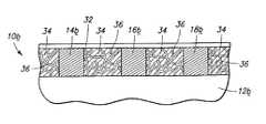
- Semiconductor wafer fragment 10 bcomprises a substrate 12 b , and conductive elements 14 b , 16 b and 18 b overlying substrate 12 b .
- Conductive elements 14 b , 16 b and 18 bmay comprise, for example, conductive lines.
- Substrate 12 bmay comprise, for example, an insulative layer over a semiconductive substrate.
- Electrical components 14 b , 16 b and 18 bare horizontally displaced from one another, with electrical components 14 b and 18 b being laterally outwardly displaced from component 16 b .
- a mass 30is between electrical components 14 b and 16 b , and between electrical components 16 b and 18 b . Mass 30 is also outwardly adjacent outer conductive elements 14 b and 18 b.
- Mass 30is preferably an insulative material and may comprise, for example, carbon.
- mass 30can comprise polyimide or photoresist.
- mass 30can comprise a mixture or a material which is substantially non-vaporizable under selected conditions, and a material which is substantially vaporizable under the selected conditions. Accordingly, complete vaporization of the substantially vaporizable material under the selected conditions will only partially vaporize mass 30 .
- mass 30can comprise a mixture of carbon and silicon dioxide.
- mass 30can comprise a mixture of carbon and SiC x .
- mass 30comprises a mixture of carbon and SiC x
- mass 30will comprise a mixture from about 20% to about 80% carbon, by volume, and from about 80% to 20% SiC x , by volume, wherein “x” is from about 0.2 to about 1.5.
- FIG. 4may be formed by a number of different methods. For instance, conductive elements 14 b , 16 b and 18 b could be formed first, and mass 30 subsequently deposited over and between conductive elements 14 b , 16 b and 18 b . Mass 30 could then be planarized to a level approximately equal with upper surfaces of conductive elements 14 b , 16 b and 18 b.
- mass 30could be deposited between an adjacent conductive lines 14 b , 16 b and 18 b , without being deposited over conductive lines 14 b , 16 b and 18 b.
- mass 30could first be formed over substrate 12 b , and subsequently conductive elements 14 b , 16 b and 18 b could be formed within mass 30 by a damascene method. Conductive electrical components 14 b , 16 b and 18 b would thereby effectively be formed within an expanse of mass 30 .
- mass 30comprises carbon
- the carbonmay be deposited by plasma decomposition of C(n)H(2n) or C(n)H(2n)X(n), wherein “X” is a halogen such as Br, Cl, I, etc.
- the deposited carbonis preferably about 10,000 Angstroms thick and can be porous. Porosity of a deposited carbon layer can be adjusted by adjusting deposition parameters, such as, plasma power, temperature, pressure, etc.
- a layer 32is formed over mass 30 , and over conductive elements 14 b , 16 b and 18 b .
- Layer 32preferably comprises a gas permeable insulative material and may comprise, for example, silicon dioxide.
- Layer 32will preferably be relatively thin, such as about 500 Angstroms thick. If layer 32 comprises silicon dioxide, the layer may be formed, for example, by sputter deposition.
- mass 30can be partially or substantially totally vaporized after provision of layer 32 .
- layer 32 and mass 30comprise materials which permit mass 30 to be partially or substantially totally vaporized under conditions which do not vaporize layer 32 .
- mass 30(shown in FIG. 5 ) is partially vaporized to form a matrix 34 between conductive elements 14 b , 16 b and 18 b .
- Matrix 34is also formed outwardly adjacent outer conductive elements 14 b and 18 b .
- Matrix 34can alternatively be referred to as a web, skeleton or scaffolding.
- the partial vaporization of mass 30can be accomplished by exposing wafer fragment 10 b to an oxidizing ambient at a temperature of from about 200° C. to about 400° C.
- oxidizing ambientsinclude, for example, O 3 , plasma O 3 , H 2 O 2 , plasma H 2 O 2 , combinations of O 3 and H 2 O 2 , and combinations of plasma O 3 and H 2 O 2 .
- the partial vaporization of mass 30occurs as excited oxygen atoms diffuse through material 32 and volatize material 34 .
- material 34comprises carbon
- the materialwill be converted into a gas comprising CO 2 and/or CO, which can diffuse out through layer 32 .
- Matrix 34comprises voids 36 . If pores were originally present in layer 30 , such pores can expand as mass 30 is vaporized to form voids 36 .
- matrix 34comprises at least one void 36 between each pair of conductive elements.
- matrix 34will comprise a plurality of voids 36 between each pair of conductive elements.
- the voids and partially vaporized material of matrix 34profile an insulative material between conductive lines 14 b and 16 b , and between conductive lines 16 b and 18 b , which preferably has a decreased dielectric constant relative to mass 30 (shown in FIG. 5 ).
- the conversion of mass 30 to partially vaporized matrix 34can advantageously decrease capacitive coupling between paired conductive elements 14 b and 16 b , and between paired conductive elements 16 b and 18 b .
- matrix 34has a dielectric constant of less than or equal to about 2.
- matrix 34provides a skeletal support structure in the embodiment of the present invention.
- Such skeletal support structurecan assist in supporting layer 32 over an expanse between paired conductive elements 14 b and 16 b , and over an expanse between paired conductive elements 16 b and 18 b .
- matrix 34can assist in supporting layer 32 outwardly adjacent outer conductive elements 14 b and 18 b .
- layer 32may be formed either before or after partial vaporization of mass 30 (shown in FIG. 5 ).
- FIGS. 7–8A second embodiment of the present invention is described with reference to FIGS. 7–8 .
- like numerals from the preceding discussion of the first embodimentare utilized, with differences being indicated by the suffix “c” or with different numerals.
- Wafer fragment 10 ccomprises a substrate 12 c .
- Conductive electrical components 14 c , 16 c and 18 coverlie substrate 12 c .
- Electrical components 14 c , 16 c and 18 care horizontally displaced from one another, with electrical components 14 c and 18 c being outwardly displaced from component 16 c .
- a mass 30 cis between electrical components 14 c and 16 c , and between electrical components 16 c and 18 c .
- Mass 30 cis also outwardly adjacent outer conductive elements 14 c and 18 c .
- Mass 30 cdoes not comprise carbon, and preferably comprises either polyimide or photoresist.
- Substrate 12 cmay comprise, for example, an insulative material over a semiconductive wafer.
- Conductive elements 14 c , 16 c and 18 cmay comprise, for example, metal lines.
- a layer 32 cis formed over mass 30 c , and over conductive elements 14 c , 16 c and 18 c .
- Layer 32 cpreferably comprises an insulative material, and may comprise, for example, silicon dioxide.
- the structure of FIG. 7is quite similar to the structure of FIG. 5 , and may therefore be formed by methods such as those discussed above regarding FIG. 5 , with the exception that mass 30 c will not comprise carbon.
- mass 30 c(shown in FIG. 7 ) is substantially totally vaporized to form voids 36 c between conductive elements 14 c , 16 c and 18 c , and outwardly adjacent outer conductive elements 14 c and 18 c .
- Mass 30 ccan be substantially totally vaporized by exposing wafer 10 c to an oxidizing ambient at a temperature of from about 200° C. to about 400° C. The difference between whether a mass such as mass 30 of FIG. 5 , or mass 30 c of FIG. 7 , is partially vaporized (as shown in FIG. 6 ) or substantially totally vaporized (as shown in FIG.
- a wafer fragmentsuch as 10 b or 10 c
- an oxidizing ambientat a temperature of from about 200° C. to about 400° C.
- the second embodiment of the present invention discussed above with reference to FIGS. 7 and 8differs from the prior art method of discussed above in the Background section in that the second embodiment utilizes an insulative layer 30 c which does not comprise carbon, such as a layer of photoresist or polyimide.
- an insulative layer 30 cwhich does not comprise carbon, such as a layer of photoresist or polyimide.
- Such use of photoresist or polyimide insulative layersoffers distinct advantages over the prior art use of carbon insulative layers. For instance, while carbon is typically applied by vapor deposition techniques, polyimide and photoresist can be applied by spin-on-wafer techniques. Spin-on-wafer techniques enable the polyimide or photoresist to be applied with a relatively planar upper surface. Such planar upper surface can eliminate planarization processes from some applications of the present invention which would otherwise require planarization processes.
- spin-on-wafer techniquesoffer an advantage in that a solvent can be incorporated into a spin-on-wafer applied layer. Such solvent can be vaporized or otherwise removed from the applied layer during vaporization of the applied layer to increase the size or amount of voids formed within the applied layer.
- the amount of solvent incorporated into a spin on-wafer applied layercan be controlled by varying the amount and type of solvent utilized during a spin-on-wafer application of a layer. For instance, a first relatively volatile solvent and a second relatively non-volatile solvent could both be utilized during a spin-on-wafer application. The first solvent would largely evaporate from an applied layer during formation of the laser while the second solvent would substantially remain within the applied layer.
- FIG. 9illustrates a third embodiment of W present invention.
- like numerals from the preceding discussion of the second embodimentare utilized with differences being indicated by the suffix “d” or with different numerals.
- a wafer fragment 10 dcomprises a substrate 12 d and conductive elements 14 d , 16 d and 18 d overlying substrate 12 d .
- a layer 32 doverlies conductive elements 14 d , 16 d and 18 d .
- Voids 36 dare formed between conductive elements 14 d , 16 d and 18 d .
- Voids 36 dcan be formed, for example by methods analogous to those discussed above with reference to FIGS. 7 and 8 , or by methods utilizing substantially total vaporization of a carbon-comprising material.
- Wafer fragment 10 dfurther comprises support members 38 formed between conductive elements 14 d and 16 d , and between conductive elements 16 d and 18 d .
- Support members 38can, advantageously assist in supporting layer 32 d over the voids 36 d between conductive elements 14 d , 16 d , and 18 d .
- Support members 38may comprise either insulative material or conductive material, but preferably do not comprise a conductive interconnect. Accordingly, support members 38 are preferably electrically isolated from conductive elements 14 d , 16 d and 18 d , as well as from other conductive structures which may be comprised by an integrated circuit formed on wafer fragment 10 d.
- Support members 38can be formed by methods readily apparent to persons of ordinary skill in the art.
- An example methodcomprises forming support members 38 between conductive elements 14 d , 16 d and 18 d and subsequently forming a mass, such as mass 30 of FIG. 5 or mass 30 c of FIG. 7 between the support members and conductive elements.
- Layer 32 dcould be then formed over the mass, over conductive elements 14 d , 16 d and 18 d , and over support members 38 .
- the masscould be either partially or substantially totally vaporized to leave voids, such as voids 36 d , between support members 38 and conductive elements 14 d , 16 d and 18 d.
- An alternative method of forming support members 38would comprise forming the support members within an expanse of a mass, such as the mass 30 of FIG. 5 , or the mass 30 c of FIG. 7 , by a damascene method.
- structure 38may be utilized with either methods of partial vaporization of insulative materials, such as the method described with reference to FIGS. 4–6 , or with methods of substantially total vaporization of insulative materials, such as the method discussed above with reference to FIGS. 7–8 .
- FIGS. 10–12A fourth embodiment of the present invention is described with reference to FIGS. 10–12 .
- like numerals from the preceding discussion of the first embodimentare utilized where appropriate, with differences being indicated with the suffix “e” or with different numerals.
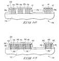
- Wafer fragment 10 ecomprises a substrate 12 e and conductive elements 14 e , 16 e , 18 e and 40 overlying substrate 12 e .
- a mass 30 eis formed over conductive elements 14 e , 16 e , 18 e and 40 , as well as between the conductive elements.
- Mass 30 epreferably comprises an insulative material, and can comprise materials such as those discussed above regarding mass 30 (shown in FIG. 4 ). Mass 30 e extends entirely from conductive element 14 e to conductive element 16 e , entirely from conductive element 16 e to conductive element 18 e , and entirely from conductive element 18 e to conductive element 40 .
- mass 30 eis anisotropically etched to remove mass 30 e from over conductive elements 14 e , 16 e , 18 e and 40 , and to remove mass 30 e from between conductive elements 18 e and 40 .
- the anisotropic etchingforms spacers 42 from mass 30 e adjacent conductive element 40 and adjacent conductive elements 14 e and 18 e.
- etching mass 30 eextends entirely from conductive element 14 e to conductive element 16 e and entirely from conductive element 16 e to conductive element 18 e , but no longer extends entirely from conductive element 18 e to conductive element 40 .
- mass 30 ewill vary depending on the chemical constituency of mass 30 e . Such methods will be readily recognized by persons of ordinary skill in the art.
- An example method for anisotropically mass 30 e when mass 30 e comprises carbonis a plasma etch utilizing O 2 .
- a layer 32 eis formed over spacers 42 , over mass 30 e , and over conductive elements 14 e , 16 e , 18 e and 40 .
- Layer 32 epreferably comprises a material porous to gas diffusion, such as a silicon dioxide layer having a thickness of about 500 Angstroms or less.
- mass 30 e(shown in FIG. 11 ) is substantially totally vaporized to form voids 36 e .
- spacers 42comprise an insulative space.
- Methods for substantially totally vaporizing mass 30 ecan include methods discussed above with reference to FIGS. 8 and 9 .
- a fifth embodiment of the present inventionis described with reference to FIG. 13 .
- like numerals from the preceding discussion of the fourth embodimentare utilized where appropriate, with differences being indicated by the suffix “f” or by different numerals.
- Wafer fragment 10 fcomprises a substrate 12 f , and conductive electrical components 14 f , 16 f , 18 f and 40 f overlying substrate 12 f .
- An insulative material 32 foverlies components 14 f , 16 f , 18 f , 40 f , and substrate 12 f .
- Wafer fragment 10 fis similar to the wafer fragment 10 e of FIG. 12 , and may be formed by similar methods.
- Wafer fragment 10 fdiffers from the wafer fragment 10 e of FIG. 12 in that wafer fragment 10 f comprises a matrix 34 f of partially vaporized material.
- Matrix 34 fcan be formed from the mass 30 e of FIG. 11 utilizing methods discussed above with reference to FIG. 6 .
- Matrix 34 fcomprises voids 36 f.
- Wafer fragment 10 ffurther comprises spacers 42 f adjacent conductive elements 14 f , 18 f and 40 f , with spacers 42 f comprising matrix 34 f and at least one void 36 f.
- material 32 fmay be formed either before or after formation of matrix 34 f.
- a sixth embodiment of the present inventionis described with reference to FIG. 14 .
- like numerals from the preceding discussion of the first five embodimentsare utilized where appropriate, with differences being indicated by the suffix “g” or by different numerals.
- Wafer fragment 10 gcomprises a substrate 12 g and conductive elements 50 , 52 , 54 , 56 , 58 , 60 , 62 and 64 .
- the sixth embodiment of FIG. 14comprises conductive elements which are vertically displaced from one another, for example, elements 50 , 52 and 54 , as well as conductive elements which are horizontally displaced from each other, for example, conductive elements 54 , 56 and 58 .
- Over conductive elements 52 , 54 , 56 , 58 , 60 , 62 and 64is a gas permeable insulative layer 32 g.
- Wafer fragment 10 gfurther comprises voids 36 g adjacent and between conductive elements 50 , 52 , 54 , 56 , 58 , 60 , 62 and 64 .
- Voids 36 gmay be formed utilizing the methods discussed above regarding the first five embodiments of the invention.
- voids 36 gmay be formed by providing a mass, analogous to mass 30 c of FIG. 7 , adjacent and between conductive elements 50 , 52 , 54 , 56 , 58 , 60 , 62 and 64 , and subsequently substantially totally vaporizing the mass to form voids 36 g .
- voids 36 gcould be formed within a matrix (not shown) analogous to matrix 34 of FIG.
- a mass analogous to mass 30 of FIG. 5may be formed adjacent and between conductive elements 50 , 52 , 54 , 56 , 58 , 60 , 62 and 64 and subsequently partially vaporized to form a matrix adjacent and between the conductive elements.
- Wafer fragment 10 gfurther comprises support members 70 , 72 , 74 , 76 and 78 .
- Support members 70 , 72 , 74 , 76 and 78may be formed by methods analogous to the methods discussed above for forming support member 38 with reference to FIG. 9 .
- Support members 70 , 72 , 74 , 76 and 78preferably comprise sizes and shapes analogous to conductive elements formed at a common elevational level with the support members.
- support members 70preferably comprise sizes and shapes analogous to that of conductive element 50 ; support members 72 preferably comprise sizes and shapes analogous to that of conductive element 52 ; support members 74 preferably comprise sizes and shapes analogous to those of conductive elements 54 , 56 and 58 ; support members 76 preferably comprise sizes and shapes similar to that of conductive element 60 ; and support members 78 preferably comprise sizes and shapes similar to those of conductive elements 62 and 64 .
- Such advantageous similarity of the sizes and shapes of support members with sizes and shapes of conductive elements at similar elevational levels to the support memberscan advantageously assist in maintaining a substantially planar upper layer 32 g.
Landscapes
- Engineering & Computer Science (AREA)
- Physics & Mathematics (AREA)
- Condensed Matter Physics & Semiconductors (AREA)
- General Physics & Mathematics (AREA)
- Computer Hardware Design (AREA)
- Microelectronics & Electronic Packaging (AREA)
- Power Engineering (AREA)
- Manufacturing & Machinery (AREA)
- Plasma & Fusion (AREA)
- Internal Circuitry In Semiconductor Integrated Circuit Devices (AREA)
Abstract
Description
Claims (15)
Priority Applications (1)
| Application Number | Priority Date | Filing Date | Title |
|---|---|---|---|
| US10/330,719US7112542B2 (en) | 1997-10-09 | 2002-12-27 | Methods of forming materials between conductive electrical components, and insulating materials |
Applications Claiming Priority (4)
| Application Number | Priority Date | Filing Date | Title |
|---|---|---|---|
| US08/947,847US6333556B1 (en) | 1997-10-09 | 1997-10-09 | Insulating materials |
| US09/115,339US6313046B1 (en) | 1997-10-09 | 1998-07-14 | Method of forming materials between conductive electrical components, and insulating materials |
| US09/976,624US6812160B2 (en) | 1997-10-09 | 2001-10-12 | Methods of forming materials between conductive electrical components, and insulating materials |
| US10/330,719US7112542B2 (en) | 1997-10-09 | 2002-12-27 | Methods of forming materials between conductive electrical components, and insulating materials |
Related Parent Applications (1)
| Application Number | Title | Priority Date | Filing Date |
|---|---|---|---|
| US09/976,624DivisionUS6812160B2 (en) | 1997-10-09 | 2001-10-12 | Methods of forming materials between conductive electrical components, and insulating materials |
Publications (2)
| Publication Number | Publication Date |
|---|---|
| US20030134503A1 US20030134503A1 (en) | 2003-07-17 |
| US7112542B2true US7112542B2 (en) | 2006-09-26 |
Family
ID=25486877
Family Applications (5)
| Application Number | Title | Priority Date | Filing Date |
|---|---|---|---|
| US08/947,847Expired - Fee RelatedUS6333556B1 (en) | 1997-10-09 | 1997-10-09 | Insulating materials |
| US09/115,339Expired - Fee RelatedUS6313046B1 (en) | 1997-10-09 | 1998-07-14 | Method of forming materials between conductive electrical components, and insulating materials |
| US09/921,861Expired - LifetimeUS6501179B2 (en) | 1997-10-09 | 2001-08-02 | Constructions comprising insulative materials |
| US09/976,624Expired - Fee RelatedUS6812160B2 (en) | 1997-10-09 | 2001-10-12 | Methods of forming materials between conductive electrical components, and insulating materials |
| US10/330,719Expired - Fee RelatedUS7112542B2 (en) | 1997-10-09 | 2002-12-27 | Methods of forming materials between conductive electrical components, and insulating materials |
Family Applications Before (4)
| Application Number | Title | Priority Date | Filing Date |
|---|---|---|---|
| US08/947,847Expired - Fee RelatedUS6333556B1 (en) | 1997-10-09 | 1997-10-09 | Insulating materials |
| US09/115,339Expired - Fee RelatedUS6313046B1 (en) | 1997-10-09 | 1998-07-14 | Method of forming materials between conductive electrical components, and insulating materials |
| US09/921,861Expired - LifetimeUS6501179B2 (en) | 1997-10-09 | 2001-08-02 | Constructions comprising insulative materials |
| US09/976,624Expired - Fee RelatedUS6812160B2 (en) | 1997-10-09 | 2001-10-12 | Methods of forming materials between conductive electrical components, and insulating materials |
Country Status (1)
| Country | Link |
|---|---|
| US (5) | US6333556B1 (en) |
Cited By (8)
| Publication number | Priority date | Publication date | Assignee | Title |
|---|---|---|---|---|
| US20050277284A1 (en)* | 2004-05-10 | 2005-12-15 | Kabushiki Kaisha Toshiba | Method for manufacturing a semiconductor device |
| US20060046322A1 (en)* | 2004-08-31 | 2006-03-02 | Micron Technology, Inc. | Integrated circuit cooling and insulating device and method |
| US20070023894A1 (en)* | 2004-12-02 | 2007-02-01 | Micron Technology, Inc. | Integrated circuit cooling system and method |
| US7276788B1 (en) | 1999-08-25 | 2007-10-02 | Micron Technology, Inc. | Hydrophobic foamed insulators for high density circuits |
| US7335965B2 (en) | 1999-08-25 | 2008-02-26 | Micron Technology, Inc. | Packaging of electronic chips with air-bridge structures |
| US20080179753A1 (en)* | 2007-01-25 | 2008-07-31 | Samsung Electronics Co., Ltd. | Semiconductor device having thermally formed air gap in wiring layer and method of fabricating same |
| US20090128991A1 (en)* | 2007-11-21 | 2009-05-21 | Micron Technology, Inc. | Methods and apparatuses for stacked capacitors for image sensors |
| US20100051578A1 (en)* | 2008-09-04 | 2010-03-04 | Shuo-Che Chang | Method for fabricating an integrated circuit |
Families Citing this family (76)
| Publication number | Priority date | Publication date | Assignee | Title |
|---|---|---|---|---|
| US7550794B2 (en) | 2002-09-20 | 2009-06-23 | Idc, Llc | Micromechanical systems device comprising a displaceable electrode and a charge-trapping layer |
| US6333556B1 (en)* | 1997-10-09 | 2001-12-25 | Micron Technology, Inc. | Insulating materials |
| US6251470B1 (en) | 1997-10-09 | 2001-06-26 | Micron Technology, Inc. | Methods of forming insulating materials, and methods of forming insulating materials around a conductive component |
| US6858526B2 (en) | 1998-07-14 | 2005-02-22 | Micron Technology, Inc. | Methods of forming materials between conductive electrical components, and insulating materials |
| US6140200A (en)* | 1998-09-02 | 2000-10-31 | Micron Technology, Inc. | Methods of forming void regions dielectric regions and capacitor constructions |
| JP2000216264A (en)* | 1999-01-22 | 2000-08-04 | Mitsubishi Electric Corp | CMOS logic circuit element, semiconductor device, method of manufacturing the same, and semiconductor circuit design method used in the method of manufacturing the same |
| US6596624B1 (en)* | 1999-07-31 | 2003-07-22 | International Business Machines Corporation | Process for making low dielectric constant hollow chip structures by removing sacrificial dielectric material after the chip is joined to a chip carrier |
| US6350679B1 (en)* | 1999-08-03 | 2002-02-26 | Micron Technology, Inc. | Methods of providing an interlevel dielectric layer intermediate different elevation conductive metal layers in the fabrication of integrated circuitry |
| WO2003007049A1 (en) | 1999-10-05 | 2003-01-23 | Iridigm Display Corporation | Photonic mems and structures |
| US6413827B2 (en) | 2000-02-14 | 2002-07-02 | Paul A. Farrar | Low dielectric constant shallow trench isolation |
| US6677209B2 (en) | 2000-02-14 | 2004-01-13 | Micron Technology, Inc. | Low dielectric constant STI with SOI devices |
| US6890847B1 (en) | 2000-02-22 | 2005-05-10 | Micron Technology, Inc. | Polynorbornene foam insulation for integrated circuits |
| KR100366768B1 (en)* | 2000-04-19 | 2003-01-09 | 삼성전자 주식회사 | A contact portion of a wirings and method manufacturing the same, and thin film transistor substrate including the contact structure and method manufacturing the same |
| US6524944B1 (en) | 2000-07-17 | 2003-02-25 | Advanced Micro Devices, Inc. | Low k ILD process by removable ILD |
| US6413852B1 (en)* | 2000-08-31 | 2002-07-02 | International Business Machines Corporation | Method of forming multilevel interconnect structure containing air gaps including utilizing both sacrificial and placeholder material |
| US6627534B1 (en)* | 2001-02-05 | 2003-09-30 | Henry F. Lee | Semiconductor fabrication process and structure with minimal capacitive coupling between conductors |
| US6852167B2 (en) | 2001-03-01 | 2005-02-08 | Micron Technology, Inc. | Methods, systems, and apparatus for uniform chemical-vapor depositions |
| JP2005510082A (en)* | 2001-11-16 | 2005-04-14 | トリコン ホールディングス リミティド | Formation of low-K dielectric layer |
| US6893984B2 (en)* | 2002-02-20 | 2005-05-17 | Micron Technology Inc. | Evaporated LaA1O3 films for gate dielectrics |
| US6734094B2 (en)* | 2002-04-29 | 2004-05-11 | Intel Corporation | Method of forming an air gap within a structure by exposing an ultraviolet sensitive material to ultraviolet radiation |
| US7160577B2 (en)* | 2002-05-02 | 2007-01-09 | Micron Technology, Inc. | Methods for atomic-layer deposition of aluminum oxides in integrated circuits |
| US7589029B2 (en) | 2002-05-02 | 2009-09-15 | Micron Technology, Inc. | Atomic layer deposition and conversion |
| US7045430B2 (en)* | 2002-05-02 | 2006-05-16 | Micron Technology Inc. | Atomic layer-deposited LaAlO3 films for gate dielectrics |
| DE10238024B4 (en)* | 2002-08-20 | 2007-03-08 | Infineon Technologies Ag | Method for integrating air as a dielectric in semiconductor devices |
| US7199023B2 (en) | 2002-08-28 | 2007-04-03 | Micron Technology, Inc. | Atomic layer deposited HfSiON dielectric films wherein each precursor is independendently pulsed |
| US7153754B2 (en)* | 2002-08-29 | 2006-12-26 | Micron Technology, Inc. | Methods for forming porous insulators from “void” creating materials and structures and semiconductor devices including same |
| US7084078B2 (en) | 2002-08-29 | 2006-08-01 | Micron Technology, Inc. | Atomic layer deposited lanthanide doped TiOx dielectric films |
| JP2006508548A (en)* | 2002-11-29 | 2006-03-09 | アドバンスト・マイクロ・ディバイシズ・インコーポレイテッド | Field effect transistor drain / source extension structure with doped high-k sidewall spacers |
| US7101813B2 (en) | 2002-12-04 | 2006-09-05 | Micron Technology Inc. | Atomic layer deposited Zr-Sn-Ti-O films |
| US6958302B2 (en) | 2002-12-04 | 2005-10-25 | Micron Technology, Inc. | Atomic layer deposited Zr-Sn-Ti-O films using TiI4 |
| US6764919B2 (en)* | 2002-12-20 | 2004-07-20 | Motorola, Inc. | Method for providing a dummy feature and structure thereof |
| US20040130027A1 (en)* | 2003-01-07 | 2004-07-08 | International Business Machines Corporation | Improved formation of porous interconnection layers |
| US20040137757A1 (en)* | 2003-01-13 | 2004-07-15 | Applied Materials, Inc. | Method and apparatus to improve cracking thresholds and mechanical properties of low-k dielectric material |
| US7192892B2 (en) | 2003-03-04 | 2007-03-20 | Micron Technology, Inc. | Atomic layer deposited dielectric layers |
| US7192824B2 (en)* | 2003-06-24 | 2007-03-20 | Micron Technology, Inc. | Lanthanide oxide / hafnium oxide dielectric layers |
| US20050137882A1 (en)* | 2003-12-17 | 2005-06-23 | Cameron Don T. | Method for authenticating goods |
| DE102004007060B3 (en)* | 2004-02-13 | 2005-07-07 | Thallner, Erich, Dipl.-Ing. | Semiconductor wafer bonding device using application of adhesive before alignment and contacting of corresponding surfaces of semiconductor wafers |
| KR100583966B1 (en)* | 2004-06-08 | 2006-05-26 | 삼성전자주식회사 | Integrated Circuit Packages With Repositioned Metal Wiring and Methods of Manufacturing the Same |
| EP2246726B1 (en) | 2004-07-29 | 2013-04-03 | QUALCOMM MEMS Technologies, Inc. | System and method for micro-electromechanical operating of an interferometric modulator |
| DE102004037336B4 (en)* | 2004-08-02 | 2006-09-21 | Infineon Technologies Ag | Method for producing a layer arrangement and layer arrangement |
| US7601649B2 (en) | 2004-08-02 | 2009-10-13 | Micron Technology, Inc. | Zirconium-doped tantalum oxide films |
| US7588988B2 (en) | 2004-08-31 | 2009-09-15 | Micron Technology, Inc. | Method of forming apparatus having oxide films formed using atomic layer deposition |
| US7369296B2 (en) | 2004-09-27 | 2008-05-06 | Idc, Llc | Device and method for modifying actuation voltage thresholds of a deformable membrane in an interferometric modulator |
| US7327510B2 (en) | 2004-09-27 | 2008-02-05 | Idc, Llc | Process for modifying offset voltage characteristics of an interferometric modulator |
| US7373026B2 (en) | 2004-09-27 | 2008-05-13 | Idc, Llc | MEMS device fabricated on a pre-patterned substrate |
| US20060125030A1 (en)* | 2004-12-13 | 2006-06-15 | Micron Technology, Inc. | Hybrid ALD-CVD of PrxOy/ZrO2 films as gate dielectrics |
| US7560395B2 (en) | 2005-01-05 | 2009-07-14 | Micron Technology, Inc. | Atomic layer deposited hafnium tantalum oxide dielectrics |
| US7662729B2 (en) | 2005-04-28 | 2010-02-16 | Micron Technology, Inc. | Atomic layer deposition of a ruthenium layer to a lanthanide oxide dielectric layer |
| US7572695B2 (en) | 2005-05-27 | 2009-08-11 | Micron Technology, Inc. | Hafnium titanium oxide films |
| US7364997B2 (en) | 2005-07-07 | 2008-04-29 | Micron Technology, Inc. | Methods of forming integrated circuitry and methods of forming local interconnects |
| US7927948B2 (en) | 2005-07-20 | 2011-04-19 | Micron Technology, Inc. | Devices with nanocrystals and methods of formation |
| EP2495212A3 (en) | 2005-07-22 | 2012-10-31 | QUALCOMM MEMS Technologies, Inc. | Mems devices having support structures and methods of fabricating the same |
| US7989290B2 (en)* | 2005-08-04 | 2011-08-02 | Micron Technology, Inc. | Methods for forming rhodium-based charge traps and apparatus including rhodium-based charge traps |
| US7575978B2 (en)* | 2005-08-04 | 2009-08-18 | Micron Technology, Inc. | Method for making conductive nanoparticle charge storage element |
| US7410910B2 (en) | 2005-08-31 | 2008-08-12 | Micron Technology, Inc. | Lanthanum aluminum oxynitride dielectric films |
| EP1928780A2 (en) | 2005-09-30 | 2008-06-11 | Qualcomm Mems Technologies, Inc. | Mems device and interconnects for same |
| US7795061B2 (en) | 2005-12-29 | 2010-09-14 | Qualcomm Mems Technologies, Inc. | Method of creating MEMS device cavities by a non-etching process |
| US7652814B2 (en) | 2006-01-27 | 2010-01-26 | Qualcomm Mems Technologies, Inc. | MEMS device with integrated optical element |
| US7709402B2 (en) | 2006-02-16 | 2010-05-04 | Micron Technology, Inc. | Conductive layers for hafnium silicon oxynitride films |
| US7450295B2 (en) | 2006-03-02 | 2008-11-11 | Qualcomm Mems Technologies, Inc. | Methods for producing MEMS with protective coatings using multi-component sacrificial layers |
| US7643203B2 (en) | 2006-04-10 | 2010-01-05 | Qualcomm Mems Technologies, Inc. | Interferometric optical display system with broadband characteristics |
| US7417784B2 (en) | 2006-04-19 | 2008-08-26 | Qualcomm Mems Technologies, Inc. | Microelectromechanical device and method utilizing a porous surface |
| US7369292B2 (en) | 2006-05-03 | 2008-05-06 | Qualcomm Mems Technologies, Inc. | Electrode and interconnect materials for MEMS devices |
| US8008144B2 (en) | 2006-05-11 | 2011-08-30 | Micron Technology, Inc. | Dual work function recessed access device and methods of forming |
| US8860174B2 (en)* | 2006-05-11 | 2014-10-14 | Micron Technology, Inc. | Recessed antifuse structures and methods of making the same |
| US20070262395A1 (en)* | 2006-05-11 | 2007-11-15 | Gibbons Jasper S | Memory cell access devices and methods of making the same |
| US7566664B2 (en) | 2006-08-02 | 2009-07-28 | Qualcomm Mems Technologies, Inc. | Selective etching of MEMS using gaseous halides and reactive co-etchants |
| US7605030B2 (en)* | 2006-08-31 | 2009-10-20 | Micron Technology, Inc. | Hafnium tantalum oxynitride high-k dielectric and metal gates |
| US7535621B2 (en) | 2006-12-27 | 2009-05-19 | Qualcomm Mems Technologies, Inc. | Aluminum fluoride films for microelectromechanical system applications |
| US7733552B2 (en) | 2007-03-21 | 2010-06-08 | Qualcomm Mems Technologies, Inc | MEMS cavity-coating layers and methods |
| US7719752B2 (en) | 2007-05-11 | 2010-05-18 | Qualcomm Mems Technologies, Inc. | MEMS structures, methods of fabricating MEMS components on separate substrates and assembly of same |
| US7570415B2 (en) | 2007-08-07 | 2009-08-04 | Qualcomm Mems Technologies, Inc. | MEMS device and interconnects for same |
| JP4929254B2 (en)* | 2008-09-02 | 2012-05-09 | 株式会社東芝 | Manufacturing method of semiconductor device |
| US7824986B2 (en) | 2008-11-05 | 2010-11-02 | Micron Technology, Inc. | Methods of forming a plurality of transistor gates, and methods of forming a plurality of transistor gates having at least two different work functions |
| KR20130025207A (en)* | 2011-09-01 | 2013-03-11 | 삼성전자주식회사 | Semiconductor device and forming the same |
| JP2015043367A (en)* | 2013-08-26 | 2015-03-05 | 株式会社東芝 | Manufacturing method of semiconductor device |
Citations (78)
| Publication number | Priority date | Publication date | Assignee | Title |
|---|---|---|---|---|
| US3767490A (en)* | 1971-06-29 | 1973-10-23 | Ibm | Process for etching organic coating layers |
| US3919060A (en) | 1974-06-14 | 1975-11-11 | Ibm | Method of fabricating semiconductor device embodying dielectric isolation |
| US3954523A (en) | 1975-04-14 | 1976-05-04 | International Business Machines Corporation | Process for fabricating devices having dielectric isolation utilizing anodic treatment and selective oxidation |
| US3979230A (en) | 1973-10-30 | 1976-09-07 | General Electric Company | Method of making isolation grids in bodies of semiconductor material |
| US3998662A (en) | 1975-12-31 | 1976-12-21 | General Electric Company | Migration of fine lines for bodies of semiconductor materials having a (100) planar orientation of a major surface |
| US4063901A (en) | 1976-03-31 | 1977-12-20 | Nippon Electric Company, Ltd. | Method of manufacturing a semiconductor device |
| US4180416A (en) | 1978-09-27 | 1979-12-25 | International Business Machines Corporation | Thermal migration-porous silicon technique for forming deep dielectric isolation |
| US4561173A (en) | 1978-11-14 | 1985-12-31 | U.S. Philips Corporation | Method of manufacturing a wiring system |
| US4572848A (en) | 1983-07-29 | 1986-02-25 | Hoechst Ceramtec Aktiengesellschaft | Process for the production of molded bodies from silicon-infiltrated, reaction-bonded silicon carbide |
| US4843034A (en) | 1987-06-12 | 1989-06-27 | Massachusetts Institute Of Technology | Fabrication of interlayer conductive paths in integrated circuits |
| US5023200A (en) | 1988-11-22 | 1991-06-11 | The United States Of America As Represented By The United States Department Of Energy | Formation of multiple levels of porous silicon for buried insulators and conductors in silicon device technologies |
| US5061514A (en) | 1990-07-13 | 1991-10-29 | Olin Corporation | Chemical vapor deposition (CVD) process for plasma depositing silicon carbide films onto a substrate |
| US5103288A (en) | 1988-03-15 | 1992-04-07 | Nec Corporation | Semiconductor device having multilayered wiring structure with a small parasitic capacitance |
| US5141896A (en) | 1990-09-18 | 1992-08-25 | Nec Corporation | Process for the production of crossing points for interconnections of semiconductor devices |
| US5149615A (en) | 1991-01-08 | 1992-09-22 | The Boeing Company | Method for producing a planar surface on which a conductive layer can be applied |
| US5165991A (en) | 1990-12-15 | 1992-11-24 | Fuji Xerox Co., Ltd. | Dielectric member for receiving an electrostatic image |
| US5171713A (en) | 1990-01-10 | 1992-12-15 | Micrunity Systems Eng | Process for forming planarized, air-bridge interconnects on a semiconductor substrate |
| US5192834A (en) | 1989-03-15 | 1993-03-09 | Sumitomo Electric Industries, Ltd. | Insulated electric wire |
| EP0542262A1 (en) | 1991-11-12 | 1993-05-19 | Nec Corporation | Method for forming a metal conductor in semiconductor device |
| US5286668A (en) | 1993-02-03 | 1994-02-15 | Industrial Technology Research Institute | Process of fabricating a high capacitance storage node |
| US5298311A (en) | 1989-12-13 | 1994-03-29 | The B. F. Goodrich Company | Moisture and oxidation resistant carbon/carbon composites |
| US5380679A (en) | 1992-10-02 | 1995-01-10 | Nec Corporation | Process for forming a multilayer wiring conductor structure in semiconductor device |
| US5380511A (en) | 1990-07-10 | 1995-01-10 | Sumitomo Metal Industries, Ltd. | Process for producing silicon carbide-base complex |
| US5461003A (en)* | 1994-05-27 | 1995-10-24 | Texas Instruments Incorporated | Multilevel interconnect structure with air gaps formed between metal leads |
| US5464786A (en) | 1994-10-24 | 1995-11-07 | Micron Technology, Inc. | Method for forming a capacitor having recessed lateral reaction barrier layer edges |
| US5466617A (en) | 1992-03-20 | 1995-11-14 | U.S. Philips Corporation | Manufacturing electronic devices comprising TFTs and MIMs |
| US5470801A (en) | 1993-06-28 | 1995-11-28 | Lsi Logic Corporation | Low dielectric constant insulation layer for integrated circuit structure and method of making same |
| US5488015A (en) | 1994-05-20 | 1996-01-30 | Texas Instruments Incorporated | Method of making an interconnect structure with an integrated low density dielectric |
| US5494858A (en) | 1994-06-07 | 1996-02-27 | Texas Instruments Incorporated | Method for forming porous composites as a low dielectric constant layer with varying porosity distribution electronics applications |
| US5496773A (en) | 1995-04-28 | 1996-03-05 | Micron Technology, Inc. | Semiconductor processing method of providing an electrically conductive interconnecting plug between an elevationally inner electrically conductive node and an elevationally outer electrically conductive node |
| US5510645A (en)* | 1993-06-02 | 1996-04-23 | Motorola, Inc. | Semiconductor structure having an air region and method of forming the semiconductor structure |
| US5525857A (en) | 1994-08-19 | 1996-06-11 | Texas Instruments Inc. | Low density, high porosity material as gate dielectric for field emission device |
| US5527737A (en) | 1994-05-27 | 1996-06-18 | Texas Instruments Incorporated | Selective formation of low-density, low-dielectric-constant insulators in narrow gaps for line-to-line capacitance reduction |
| US5543346A (en)* | 1993-08-31 | 1996-08-06 | Hyundai Electronics Industries Co., Ltd. | Method of fabricating a dynamic random access memory stacked capacitor |
| US5554567A (en) | 1994-09-01 | 1996-09-10 | Taiwan Semiconductor Manufacturing Company Ltd. | Method for improving adhesion to a spin-on-glass |
| US5583078A (en) | 1991-04-30 | 1996-12-10 | Lucent Technologies Inc. | Method for fabricating a planar dielectric |
| US5599745A (en) | 1995-06-07 | 1997-02-04 | Micron Technology, Inc. | Method to provide a void between adjacent conducting lines in a semiconductor device |
| US5629238A (en) | 1994-11-30 | 1997-05-13 | Samsung Electronics Co., Ltd. | Method for forming conductive line of semiconductor device |
| US5670828A (en) | 1995-02-21 | 1997-09-23 | Advanced Micro Devices, Inc. | Tunneling technology for reducing intra-conductive layer capacitance |
| US5674787A (en) | 1996-01-16 | 1997-10-07 | Sematech, Inc. | Selective electroless copper deposited interconnect plugs for ULSI applications |
| US5691565A (en) | 1995-12-27 | 1997-11-25 | Micron Technology, Inc. | Integrated circuitry having a pair of adjacent conductive lines |
| US5691573A (en) | 1995-06-07 | 1997-11-25 | Advanced Micro Devices, Inc. | Composite insulation with a dielectric constant of less than 3 in a narrow space separating conductive lines |
| US5723368A (en) | 1994-06-23 | 1998-03-03 | Cho; Chi-Chen | Porous dielectric material with improved pore surface properties for electronics applications |
| US5736425A (en) | 1995-11-16 | 1998-04-07 | Texas Instruments Incorporated | Glycol-based method for forming a thin-film nanoporous dielectric |
| US5736459A (en) | 1997-05-15 | 1998-04-07 | Vanguard International Semiconductor Corporation | Method to fabricate a polysilicon stud using an oxygen ion implantation procedure |
| US5744399A (en) | 1995-11-13 | 1998-04-28 | Lsi Logic Corporation | Process for forming low dielectric constant layers using fullerenes |
| US5750415A (en) | 1994-05-27 | 1998-05-12 | Texas Instruments Incorporated | Low dielectric constant layers via immiscible sol-gel processing |
| US5773363A (en) | 1994-11-08 | 1998-06-30 | Micron Technology, Inc. | Semiconductor processing method of making electrical contact to a node |
| US5804508A (en) | 1994-05-20 | 1998-09-08 | Texas Instruments Incorporated | Method of making a low dielectric constant material for electronics |
| US5807607A (en) | 1995-11-16 | 1998-09-15 | Texas Instruments Incorporated | Polyol-based method for forming thin film aerogels on semiconductor substrates |
| US5858871A (en) | 1994-05-27 | 1999-01-12 | Texas Instruments Incorporated | Porous insulator for line-to-line capacitance reduction |
| US5861345A (en) | 1995-05-01 | 1999-01-19 | Chou; Chin-Hao | In-situ pre-PECVD oxide deposition process for treating SOG |
| US5883014A (en) | 1997-06-03 | 1999-03-16 | United Microelectronics Corp. | Method for treating via sidewalls with hydrogen plasma |
| US5882978A (en) | 1996-10-30 | 1999-03-16 | Micron Technology, Inc. | Methods of forming a silicon nitride film, a capacitor dielectric layer and a capacitor |
| EP0923125A1 (en) | 1997-11-28 | 1999-06-16 | STMicroelectronics SA | Method of making metallic interconnections in integrated circuits |
| US5950102A (en) | 1997-02-03 | 1999-09-07 | Industrial Technology Research Institute | Method for fabricating air-insulated multilevel metal interconnections for integrated circuits |
| US5967804A (en) | 1987-03-04 | 1999-10-19 | Canon Kabushiki Kaisha | Circuit member and electric circuit device with the connecting member |
| US5970360A (en) | 1996-12-03 | 1999-10-19 | Mosel Vitelic Inc. | DRAM cell with a roughened poly-Si electrode |
| US5981085A (en) | 1996-03-21 | 1999-11-09 | The Furukawa Electric Co., Inc. | Composite substrate for heat-generating semiconductor device and semiconductor apparatus using the same |
| US6001747A (en) | 1998-07-22 | 1999-12-14 | Vlsi Technology, Inc. | Process to improve adhesion of cap layers in integrated circuits |
| US6008540A (en) | 1997-05-28 | 1999-12-28 | Texas Instruments Incorporated | Integrated circuit dielectric and method |
| US6028015A (en) | 1999-03-29 | 2000-02-22 | Lsi Logic Corporation | Process for treating damaged surfaces of low dielectric constant organo silicon oxide insulation material to inhibit moisture absorption |
| US6039847A (en) | 1997-06-23 | 2000-03-21 | Agency Of Industrial Science & Technology | Method of forming a highly pure thin film and apparatus therefor |
| US6143645A (en) | 1997-02-03 | 2000-11-07 | Texas Instruments Incorporated | Reduced temperature contact/via filling |
| US6156374A (en) | 1997-10-09 | 2000-12-05 | Micron Technology, Inc. | Method of forming insulating material between components of an integrated circuit |
| US6184572B1 (en) | 1998-04-29 | 2001-02-06 | Novellus Systems, Inc. | Interlevel dielectric stack containing plasma deposited fluorinated amorphous carbon films for semiconductor devices |
| US6204172B1 (en) | 1998-09-03 | 2001-03-20 | Micron Technology, Inc. | Low temperature deposition of barrier layers |
| US6207583B1 (en) | 1998-09-04 | 2001-03-27 | Alliedsignal Inc. | Photoresist ashing process for organic and inorganic polymer dielectric materials |
| US6245439B1 (en) | 1994-08-09 | 2001-06-12 | Kabushiki Kaisha Toyoyta Chuo Kenkyusho | composite material and method for the manufacture |
| US6271146B1 (en) | 1999-09-30 | 2001-08-07 | Electron Vision Corporation | Electron beam treatment of fluorinated silicate glass |
| US6313046B1 (en) | 1997-10-09 | 2001-11-06 | Micron Technology, Inc. | Method of forming materials between conductive electrical components, and insulating materials |
| US6319852B1 (en) | 1995-11-16 | 2001-11-20 | Texas Instruments Incorporated | Nanoporous dielectric thin film formation using a post-deposition catalyst |
| US6347446B1 (en) | 1997-01-13 | 2002-02-19 | General Electric Company | Method of making silicon carbide-silicon composite having improved oxidation resistance |
| US6351039B1 (en) | 1997-05-28 | 2002-02-26 | Texas Instruments Incorporated | Integrated circuit dielectric and method |
| US6350679B1 (en) | 1999-08-03 | 2002-02-26 | Micron Technology, Inc. | Methods of providing an interlevel dielectric layer intermediate different elevation conductive metal layers in the fabrication of integrated circuitry |
| US6448187B2 (en) | 1998-11-04 | 2002-09-10 | Applied Materials, Inc. | Method of improving moisture resistance of low dielectric constant films |
| US6495458B2 (en) | 1998-09-03 | 2002-12-17 | Micron Technology, Inc. | Method for producing low carbon/oxygen conductive layers |
| US6589887B1 (en) | 2001-10-11 | 2003-07-08 | Novellus Systems, Inc. | Forming metal-derived layers by simultaneous deposition and evaporation of metal |
Family Cites Families (1)
| Publication number | Priority date | Publication date | Assignee | Title |
|---|---|---|---|---|
| US6153374A (en) | 1994-12-13 | 2000-11-28 | Novartis Finance Corporation | Method for identifying inhibitors of soraphen A resistant acetyl-coenzyme a carboxylase |
- 1997
- 1997-10-09USUS08/947,847patent/US6333556B1/ennot_activeExpired - Fee Related
- 1998
- 1998-07-14USUS09/115,339patent/US6313046B1/ennot_activeExpired - Fee Related
- 2001
- 2001-08-02USUS09/921,861patent/US6501179B2/ennot_activeExpired - Lifetime
- 2001-10-12USUS09/976,624patent/US6812160B2/ennot_activeExpired - Fee Related
- 2002
- 2002-12-27USUS10/330,719patent/US7112542B2/ennot_activeExpired - Fee Related
Patent Citations (85)
| Publication number | Priority date | Publication date | Assignee | Title |
|---|---|---|---|---|
| US3767490A (en)* | 1971-06-29 | 1973-10-23 | Ibm | Process for etching organic coating layers |
| US3979230A (en) | 1973-10-30 | 1976-09-07 | General Electric Company | Method of making isolation grids in bodies of semiconductor material |
| US3919060A (en) | 1974-06-14 | 1975-11-11 | Ibm | Method of fabricating semiconductor device embodying dielectric isolation |
| US3954523A (en) | 1975-04-14 | 1976-05-04 | International Business Machines Corporation | Process for fabricating devices having dielectric isolation utilizing anodic treatment and selective oxidation |
| US3998662A (en) | 1975-12-31 | 1976-12-21 | General Electric Company | Migration of fine lines for bodies of semiconductor materials having a (100) planar orientation of a major surface |
| US4063901A (en) | 1976-03-31 | 1977-12-20 | Nippon Electric Company, Ltd. | Method of manufacturing a semiconductor device |
| US4180416A (en) | 1978-09-27 | 1979-12-25 | International Business Machines Corporation | Thermal migration-porous silicon technique for forming deep dielectric isolation |
| US4561173A (en) | 1978-11-14 | 1985-12-31 | U.S. Philips Corporation | Method of manufacturing a wiring system |
| US4572848A (en) | 1983-07-29 | 1986-02-25 | Hoechst Ceramtec Aktiengesellschaft | Process for the production of molded bodies from silicon-infiltrated, reaction-bonded silicon carbide |
| US5967804A (en) | 1987-03-04 | 1999-10-19 | Canon Kabushiki Kaisha | Circuit member and electric circuit device with the connecting member |
| US4843034A (en) | 1987-06-12 | 1989-06-27 | Massachusetts Institute Of Technology | Fabrication of interlayer conductive paths in integrated circuits |
| US5103288A (en) | 1988-03-15 | 1992-04-07 | Nec Corporation | Semiconductor device having multilayered wiring structure with a small parasitic capacitance |
| US5023200A (en) | 1988-11-22 | 1991-06-11 | The United States Of America As Represented By The United States Department Of Energy | Formation of multiple levels of porous silicon for buried insulators and conductors in silicon device technologies |
| US5192834A (en) | 1989-03-15 | 1993-03-09 | Sumitomo Electric Industries, Ltd. | Insulated electric wire |
| US5298311A (en) | 1989-12-13 | 1994-03-29 | The B. F. Goodrich Company | Moisture and oxidation resistant carbon/carbon composites |
| US5171713A (en) | 1990-01-10 | 1992-12-15 | Micrunity Systems Eng | Process for forming planarized, air-bridge interconnects on a semiconductor substrate |
| US5380511A (en) | 1990-07-10 | 1995-01-10 | Sumitomo Metal Industries, Ltd. | Process for producing silicon carbide-base complex |
| US5061514A (en) | 1990-07-13 | 1991-10-29 | Olin Corporation | Chemical vapor deposition (CVD) process for plasma depositing silicon carbide films onto a substrate |
| US5141896A (en) | 1990-09-18 | 1992-08-25 | Nec Corporation | Process for the production of crossing points for interconnections of semiconductor devices |
| US5165991A (en) | 1990-12-15 | 1992-11-24 | Fuji Xerox Co., Ltd. | Dielectric member for receiving an electrostatic image |
| US5149615A (en) | 1991-01-08 | 1992-09-22 | The Boeing Company | Method for producing a planar surface on which a conductive layer can be applied |
| US5583078A (en) | 1991-04-30 | 1996-12-10 | Lucent Technologies Inc. | Method for fabricating a planar dielectric |
| EP0542262A1 (en) | 1991-11-12 | 1993-05-19 | Nec Corporation | Method for forming a metal conductor in semiconductor device |
| US5266519A (en) | 1991-11-12 | 1993-11-30 | Nec Corporation | Method for forming a metal conductor in semiconductor device |
| US5466617A (en) | 1992-03-20 | 1995-11-14 | U.S. Philips Corporation | Manufacturing electronic devices comprising TFTs and MIMs |
| US5380679A (en) | 1992-10-02 | 1995-01-10 | Nec Corporation | Process for forming a multilayer wiring conductor structure in semiconductor device |
| US5286668A (en) | 1993-02-03 | 1994-02-15 | Industrial Technology Research Institute | Process of fabricating a high capacitance storage node |
| US5510645A (en)* | 1993-06-02 | 1996-04-23 | Motorola, Inc. | Semiconductor structure having an air region and method of forming the semiconductor structure |
| US5470801A (en) | 1993-06-28 | 1995-11-28 | Lsi Logic Corporation | Low dielectric constant insulation layer for integrated circuit structure and method of making same |
| US5543346A (en)* | 1993-08-31 | 1996-08-06 | Hyundai Electronics Industries Co., Ltd. | Method of fabricating a dynamic random access memory stacked capacitor |
| US5488015A (en) | 1994-05-20 | 1996-01-30 | Texas Instruments Incorporated | Method of making an interconnect structure with an integrated low density dielectric |
| US5804508A (en) | 1994-05-20 | 1998-09-08 | Texas Instruments Incorporated | Method of making a low dielectric constant material for electronics |
| US5750415A (en) | 1994-05-27 | 1998-05-12 | Texas Instruments Incorporated | Low dielectric constant layers via immiscible sol-gel processing |
| US5461003A (en)* | 1994-05-27 | 1995-10-24 | Texas Instruments Incorporated | Multilevel interconnect structure with air gaps formed between metal leads |
| US5858871A (en) | 1994-05-27 | 1999-01-12 | Texas Instruments Incorporated | Porous insulator for line-to-line capacitance reduction |
| US5527737A (en) | 1994-05-27 | 1996-06-18 | Texas Instruments Incorporated | Selective formation of low-density, low-dielectric-constant insulators in narrow gaps for line-to-line capacitance reduction |
| US5494858A (en) | 1994-06-07 | 1996-02-27 | Texas Instruments Incorporated | Method for forming porous composites as a low dielectric constant layer with varying porosity distribution electronics applications |
| US5847443A (en) | 1994-06-23 | 1998-12-08 | Texas Instruments Incorporated | Porous dielectric material with improved pore surface properties for electronics applications |
| US5723368A (en) | 1994-06-23 | 1998-03-03 | Cho; Chi-Chen | Porous dielectric material with improved pore surface properties for electronics applications |
| US6245439B1 (en) | 1994-08-09 | 2001-06-12 | Kabushiki Kaisha Toyoyta Chuo Kenkyusho | composite material and method for the manufacture |
| US5525857A (en) | 1994-08-19 | 1996-06-11 | Texas Instruments Inc. | Low density, high porosity material as gate dielectric for field emission device |
| US5554567A (en) | 1994-09-01 | 1996-09-10 | Taiwan Semiconductor Manufacturing Company Ltd. | Method for improving adhesion to a spin-on-glass |
| US5559666A (en) | 1994-10-24 | 1996-09-24 | Micron Technology, Inc. | Capacitor construction with oxidation barrier blocks |
| US5808854A (en) | 1994-10-24 | 1998-09-15 | Micron Technology, Inc. | Capacitor construction with oxidation barrier blocks |
| US5654224A (en) | 1994-10-24 | 1997-08-05 | Micron Technology, Inc. | Capacitor construction with oxidation barrier blocks |
| US5464786A (en) | 1994-10-24 | 1995-11-07 | Micron Technology, Inc. | Method for forming a capacitor having recessed lateral reaction barrier layer edges |
| US5773363A (en) | 1994-11-08 | 1998-06-30 | Micron Technology, Inc. | Semiconductor processing method of making electrical contact to a node |
| US5629238A (en) | 1994-11-30 | 1997-05-13 | Samsung Electronics Co., Ltd. | Method for forming conductive line of semiconductor device |
| US5670828A (en) | 1995-02-21 | 1997-09-23 | Advanced Micro Devices, Inc. | Tunneling technology for reducing intra-conductive layer capacitance |
| US5496773A (en) | 1995-04-28 | 1996-03-05 | Micron Technology, Inc. | Semiconductor processing method of providing an electrically conductive interconnecting plug between an elevationally inner electrically conductive node and an elevationally outer electrically conductive node |
| US5861345A (en) | 1995-05-01 | 1999-01-19 | Chou; Chin-Hao | In-situ pre-PECVD oxide deposition process for treating SOG |
| US5691573A (en) | 1995-06-07 | 1997-11-25 | Advanced Micro Devices, Inc. | Composite insulation with a dielectric constant of less than 3 in a narrow space separating conductive lines |
| US5599745A (en) | 1995-06-07 | 1997-02-04 | Micron Technology, Inc. | Method to provide a void between adjacent conducting lines in a semiconductor device |
| US5744399A (en) | 1995-11-13 | 1998-04-28 | Lsi Logic Corporation | Process for forming low dielectric constant layers using fullerenes |
| US5807607A (en) | 1995-11-16 | 1998-09-15 | Texas Instruments Incorporated | Polyol-based method for forming thin film aerogels on semiconductor substrates |
| US6319852B1 (en) | 1995-11-16 | 2001-11-20 | Texas Instruments Incorporated | Nanoporous dielectric thin film formation using a post-deposition catalyst |
| US5736425A (en) | 1995-11-16 | 1998-04-07 | Texas Instruments Incorporated | Glycol-based method for forming a thin-film nanoporous dielectric |
| US5691565A (en) | 1995-12-27 | 1997-11-25 | Micron Technology, Inc. | Integrated circuitry having a pair of adjacent conductive lines |
| US5674787A (en) | 1996-01-16 | 1997-10-07 | Sematech, Inc. | Selective electroless copper deposited interconnect plugs for ULSI applications |
| US5981085A (en) | 1996-03-21 | 1999-11-09 | The Furukawa Electric Co., Inc. | Composite substrate for heat-generating semiconductor device and semiconductor apparatus using the same |
| US5882978A (en) | 1996-10-30 | 1999-03-16 | Micron Technology, Inc. | Methods of forming a silicon nitride film, a capacitor dielectric layer and a capacitor |
| US5970360A (en) | 1996-12-03 | 1999-10-19 | Mosel Vitelic Inc. | DRAM cell with a roughened poly-Si electrode |
| US6347446B1 (en) | 1997-01-13 | 2002-02-19 | General Electric Company | Method of making silicon carbide-silicon composite having improved oxidation resistance |
| US5950102A (en) | 1997-02-03 | 1999-09-07 | Industrial Technology Research Institute | Method for fabricating air-insulated multilevel metal interconnections for integrated circuits |
| US6143645A (en) | 1997-02-03 | 2000-11-07 | Texas Instruments Incorporated | Reduced temperature contact/via filling |
| US5736459A (en) | 1997-05-15 | 1998-04-07 | Vanguard International Semiconductor Corporation | Method to fabricate a polysilicon stud using an oxygen ion implantation procedure |
| US6008540A (en) | 1997-05-28 | 1999-12-28 | Texas Instruments Incorporated | Integrated circuit dielectric and method |
| US6351039B1 (en) | 1997-05-28 | 2002-02-26 | Texas Instruments Incorporated | Integrated circuit dielectric and method |
| US5883014A (en) | 1997-06-03 | 1999-03-16 | United Microelectronics Corp. | Method for treating via sidewalls with hydrogen plasma |
| US6039847A (en) | 1997-06-23 | 2000-03-21 | Agency Of Industrial Science & Technology | Method of forming a highly pure thin film and apparatus therefor |
| US6313046B1 (en) | 1997-10-09 | 2001-11-06 | Micron Technology, Inc. | Method of forming materials between conductive electrical components, and insulating materials |
| US6156374A (en) | 1997-10-09 | 2000-12-05 | Micron Technology, Inc. | Method of forming insulating material between components of an integrated circuit |
| US6333556B1 (en) | 1997-10-09 | 2001-12-25 | Micron Technology, Inc. | Insulating materials |
| US6251470B1 (en) | 1997-10-09 | 2001-06-26 | Micron Technology, Inc. | Methods of forming insulating materials, and methods of forming insulating materials around a conductive component |
| EP0923125A1 (en) | 1997-11-28 | 1999-06-16 | STMicroelectronics SA | Method of making metallic interconnections in integrated circuits |
| US6184572B1 (en) | 1998-04-29 | 2001-02-06 | Novellus Systems, Inc. | Interlevel dielectric stack containing plasma deposited fluorinated amorphous carbon films for semiconductor devices |
| US6001747A (en) | 1998-07-22 | 1999-12-14 | Vlsi Technology, Inc. | Process to improve adhesion of cap layers in integrated circuits |
| US6204172B1 (en) | 1998-09-03 | 2001-03-20 | Micron Technology, Inc. | Low temperature deposition of barrier layers |
| US6495458B2 (en) | 1998-09-03 | 2002-12-17 | Micron Technology, Inc. | Method for producing low carbon/oxygen conductive layers |
| US6207583B1 (en) | 1998-09-04 | 2001-03-27 | Alliedsignal Inc. | Photoresist ashing process for organic and inorganic polymer dielectric materials |
| US6448187B2 (en) | 1998-11-04 | 2002-09-10 | Applied Materials, Inc. | Method of improving moisture resistance of low dielectric constant films |
| US6028015A (en) | 1999-03-29 | 2000-02-22 | Lsi Logic Corporation | Process for treating damaged surfaces of low dielectric constant organo silicon oxide insulation material to inhibit moisture absorption |
| US6350679B1 (en) | 1999-08-03 | 2002-02-26 | Micron Technology, Inc. | Methods of providing an interlevel dielectric layer intermediate different elevation conductive metal layers in the fabrication of integrated circuitry |
| US6271146B1 (en) | 1999-09-30 | 2001-08-07 | Electron Vision Corporation | Electron beam treatment of fluorinated silicate glass |
| US6589887B1 (en) | 2001-10-11 | 2003-07-08 | Novellus Systems, Inc. | Forming metal-derived layers by simultaneous deposition and evaporation of metal |
Non-Patent Citations (12)
| Title |
|---|
| Abstract: Anderson, R.C. et al., "Porous Polycrystalline Silicon: A New Material For MEMS", Jnl. of Microelectromechanical Systems (Mar. 1994), vol. 3, No. 1, pp. 10-18. |
| Anand, M.B., "NURA: A Feasible, Gas-Dielectric Interconnect Process", 1996 Sympos. on VLSI Technology Digest of Technical Papers, IEEE 1996, pp. 82-83. |
| Gayes, et al., Translation of EP 0923125 A1, "Process For Making Metal Interconnections In Integrated Circuits," Jun. 1999. |
| J. H. Lee et al., "Fabrication of Surface Micromachined Polysilicon Actuators Using Dry Release Process of HF Gas-Phase Etching" International Electron Devices Meeting, San Francisco, CA, 1996, IEDM 96, pp. 761-764.* |
| P. Townsend et al., "SiLK Polymer Coating with Low Dielectric Constant and High Thermal Stability for VLSI Interlayer Dielectric", Proceedings Materials Research Society San Francisco, CA, Apr. 1997, vol. 476, pp. 9-17. |
| Peter Singer (Editor-in-Chief); "The New Low-k Candidate: It's a Gas"; Technology News, Mar. 1989; 1 page. |
| Product Brochure and Material Safety Data Sheet, "Interlayer Dielectric", JSR Microelectronics, 12 Pages (1997). Year is sufficiently early so that the month is not an issue. |
| Stanley Wolf Ph.D., Silicon Processing for the VLSI Era, (c) 1986, pp. 1-8. |
| Stanley Wolf Ph.D., Silicon Processing for the VLSI Era, (c) 1986, pp. 429-437. |
| Togo, M., "A Gate-side Air-gap Structure (GAS) to Reduce the Parasitic Capacitance in MOSFETs", 1996 Sympos. on VLSI Technology Digest of Technical Papers, IEEE 1996, pp. 38-39. |
| Watanabe, H., "A Novel Stacked Capacitor with Porous-Si Electrodes for High Density DRAMs", 1993 Symposium on VLSI Technology, Digest of Technical Papers, Kyoto Japan, 17-18, 1993. Year is sufficiently early so that the month is not an issue. |
| Wolf, et al. Silicon Processing for the VLSI Era, vol. 1-Process Technology, Lattice Press: Sunset Beach CA, 1986, pp. 428-429.* |
Cited By (18)
| Publication number | Priority date | Publication date | Assignee | Title |
|---|---|---|---|---|
| US7387912B2 (en)* | 1999-08-25 | 2008-06-17 | Micron Technology, Inc. | Packaging of electronic chips with air-bridge structures |
| US7335965B2 (en) | 1999-08-25 | 2008-02-26 | Micron Technology, Inc. | Packaging of electronic chips with air-bridge structures |
| US7276788B1 (en) | 1999-08-25 | 2007-10-02 | Micron Technology, Inc. | Hydrophobic foamed insulators for high density circuits |
| US20050277284A1 (en)* | 2004-05-10 | 2005-12-15 | Kabushiki Kaisha Toshiba | Method for manufacturing a semiconductor device |
| US7300821B2 (en) | 2004-08-31 | 2007-11-27 | Micron Technology, Inc. | Integrated circuit cooling and insulating device and method |
| US7485497B2 (en) | 2004-08-31 | 2009-02-03 | Micron Technology, Inc. | Integrated circuit cooling and insulating device and method |
| US20080048314A1 (en)* | 2004-08-31 | 2008-02-28 | Micron Technology, Inc. | Integrated circuit cooling and insulating device and method |
| US20080057629A1 (en)* | 2004-08-31 | 2008-03-06 | Micron Technology, Inc. | Integrated circuit cooling and insulating device and method |
| US20060046322A1 (en)* | 2004-08-31 | 2006-03-02 | Micron Technology, Inc. | Integrated circuit cooling and insulating device and method |
| US7492042B2 (en) | 2004-08-31 | 2009-02-17 | Micron Technology, Inc. | Integrated circuit cooling and insulating device and method |
| US7489034B2 (en) | 2004-12-02 | 2009-02-10 | Micron Technology, Inc. | Integrated circuit cooling system and method |
| US20070023894A1 (en)* | 2004-12-02 | 2007-02-01 | Micron Technology, Inc. | Integrated circuit cooling system and method |
| US20080179753A1 (en)* | 2007-01-25 | 2008-07-31 | Samsung Electronics Co., Ltd. | Semiconductor device having thermally formed air gap in wiring layer and method of fabricating same |
| US7892966B2 (en)* | 2007-01-25 | 2011-02-22 | Samsung Electronics Co., Ltd. | Semiconductor device having thermally formed air gap in wiring layer and method of fabricating same |
| US20110101492A1 (en)* | 2007-01-25 | 2011-05-05 | Samsung Electronics Co., Ltd. | Semiconductor device having thermally formed air gap in wiring layer and method of fabricating same |
| US8198701B2 (en) | 2007-01-25 | 2012-06-12 | Samsung Electronics Co., Ltd. | Semiconductor device having thermally formed air gap in wiring layer and method of fabricating same |
| US20090128991A1 (en)* | 2007-11-21 | 2009-05-21 | Micron Technology, Inc. | Methods and apparatuses for stacked capacitors for image sensors |
| US20100051578A1 (en)* | 2008-09-04 | 2010-03-04 | Shuo-Che Chang | Method for fabricating an integrated circuit |
Also Published As
| Publication number | Publication date |
|---|---|
| US6313046B1 (en) | 2001-11-06 |
| US6812160B2 (en) | 2004-11-02 |
| US6501179B2 (en) | 2002-12-31 |
| US20030134503A1 (en) | 2003-07-17 |
| US6333556B1 (en) | 2001-12-25 |
| US20010050438A1 (en) | 2001-12-13 |
| US20020019125A1 (en) | 2002-02-14 |
Similar Documents
| Publication | Publication Date | Title |
|---|---|---|
| US7112542B2 (en) | Methods of forming materials between conductive electrical components, and insulating materials | |
| US7262503B2 (en) | Semiconductor constructions | |
| US5110712A (en) | Incorporation of dielectric layers in a semiconductor | |
| US4987101A (en) | Method for providing improved insulation in VLSI and ULSI circuits | |
| US6368518B1 (en) | Methods for removing rhodium- and iridium-containing films | |
| US6284644B1 (en) | IMD scheme by post-plasma treatment of FSG and TEOS oxide capping layer | |
| US6326300B1 (en) | Dual damascene patterned conductor layer formation method | |
| US6232217B1 (en) | Post treatment of via opening by N-containing plasma or H-containing plasma for elimination of fluorine species in the FSG near the surfaces of the via opening | |
| US6424044B1 (en) | Use of boron carbide as an etch-stop and barrier layer for copper dual damascene metallization | |
| US4523975A (en) | Integrated circuit planarizing process | |
| US6459562B1 (en) | High density metal insulator metal capacitors | |
| US6987066B2 (en) | Dry etching method and semiconductor device manufacturing method | |
| US7071094B2 (en) | Dual layer barrier film techniques to prevent resist poisoning | |
| US7022582B2 (en) | Microelectronic process and structure | |
| US5366850A (en) | Submicron planarization process with passivation on metal line | |
| KR20020073393A (en) | Method for manufacturing a semiconductor device having a ruthenium or a ruthenium oxide | |
| US6117764A (en) | Use of a plasma source to form a layer during the formation of a semiconductor device | |
| US6770575B2 (en) | Method for improving thermal stability of fluorinated amorphous carbon low dielectric constant materials | |
| EP0981161A2 (en) | Semiconductor structure including a conductive fuse and process for fabrication thereof | |
| US7709343B2 (en) | Use of a plasma source to form a layer during the formation of a semiconductor device | |
| EP0296707A1 (en) | Incorporation of dielectric layers in a semiconductor | |
| GB2300303A (en) | Etching silicon oxide during semiconductor manufacture | |
| US5869406A (en) | Method for forming insulating layers between polysilicon layers | |
| US6472330B1 (en) | Method for forming an interlayer insulating film, and semiconductor device | |
| KR100585082B1 (en) | Contact hole formation method of semiconductor device |
Legal Events
| Date | Code | Title | Description |
|---|---|---|---|
| FEPP | Fee payment procedure | Free format text:PAYOR NUMBER ASSIGNED (ORIGINAL EVENT CODE: ASPN); ENTITY STATUS OF PATENT OWNER: LARGE ENTITY | |
| CC | Certificate of correction | ||
| FPAY | Fee payment | Year of fee payment:4 | |
| FPAY | Fee payment | Year of fee payment:8 | |
| AS | Assignment | Owner name:U.S. BANK NATIONAL ASSOCIATION, AS COLLATERAL AGENT, CALIFORNIA Free format text:SECURITY INTEREST;ASSIGNOR:MICRON TECHNOLOGY, INC.;REEL/FRAME:038669/0001 Effective date:20160426 Owner name:U.S. BANK NATIONAL ASSOCIATION, AS COLLATERAL AGEN Free format text:SECURITY INTEREST;ASSIGNOR:MICRON TECHNOLOGY, INC.;REEL/FRAME:038669/0001 Effective date:20160426 | |
| AS | Assignment | Owner name:MORGAN STANLEY SENIOR FUNDING, INC., AS COLLATERAL AGENT, MARYLAND Free format text:PATENT SECURITY AGREEMENT;ASSIGNOR:MICRON TECHNOLOGY, INC.;REEL/FRAME:038954/0001 Effective date:20160426 Owner name:MORGAN STANLEY SENIOR FUNDING, INC., AS COLLATERAL Free format text:PATENT SECURITY AGREEMENT;ASSIGNOR:MICRON TECHNOLOGY, INC.;REEL/FRAME:038954/0001 Effective date:20160426 | |
| AS | Assignment | Owner name:U.S. BANK NATIONAL ASSOCIATION, AS COLLATERAL AGENT, CALIFORNIA Free format text:CORRECTIVE ASSIGNMENT TO CORRECT THE REPLACE ERRONEOUSLY FILED PATENT #7358718 WITH THE CORRECT PATENT #7358178 PREVIOUSLY RECORDED ON REEL 038669 FRAME 0001. ASSIGNOR(S) HEREBY CONFIRMS THE SECURITY INTEREST;ASSIGNOR:MICRON TECHNOLOGY, INC.;REEL/FRAME:043079/0001 Effective date:20160426 Owner name:U.S. BANK NATIONAL ASSOCIATION, AS COLLATERAL AGEN Free format text:CORRECTIVE ASSIGNMENT TO CORRECT THE REPLACE ERRONEOUSLY FILED PATENT #7358718 WITH THE CORRECT PATENT #7358178 PREVIOUSLY RECORDED ON REEL 038669 FRAME 0001. ASSIGNOR(S) HEREBY CONFIRMS THE SECURITY INTEREST;ASSIGNOR:MICRON TECHNOLOGY, INC.;REEL/FRAME:043079/0001 Effective date:20160426 | |
| FEPP | Fee payment procedure | Free format text:MAINTENANCE FEE REMINDER MAILED (ORIGINAL EVENT CODE: REM.) | |
| AS | Assignment | Owner name:MICRON TECHNOLOGY, INC., IDAHO Free format text:RELEASE BY SECURED PARTY;ASSIGNOR:U.S. BANK NATIONAL ASSOCIATION, AS COLLATERAL AGENT;REEL/FRAME:047243/0001 Effective date:20180629 | |
| LAPS | Lapse for failure to pay maintenance fees | Free format text:PATENT EXPIRED FOR FAILURE TO PAY MAINTENANCE FEES (ORIGINAL EVENT CODE: EXP.); ENTITY STATUS OF PATENT OWNER: LARGE ENTITY | |
| STCH | Information on status: patent discontinuation | Free format text:PATENT EXPIRED DUE TO NONPAYMENT OF MAINTENANCE FEES UNDER 37 CFR 1.362 | |
| FP | Lapsed due to failure to pay maintenance fee | Effective date:20180926 | |
| AS | Assignment | Owner name:MICRON TECHNOLOGY, INC., IDAHO Free format text:RELEASE BY SECURED PARTY;ASSIGNOR:MORGAN STANLEY SENIOR FUNDING, INC., AS COLLATERAL AGENT;REEL/FRAME:050937/0001 Effective date:20190731 |