US7112454B2 - System and method for reducing shorting in memory cells - Google Patents
System and method for reducing shorting in memory cellsDownload PDFInfo
- Publication number
- US7112454B2 US7112454B2US10/684,967US68496703AUS7112454B2US 7112454 B2US7112454 B2US 7112454B2US 68496703 AUS68496703 AUS 68496703AUS 7112454 B2US7112454 B2US 7112454B2
- Authority
- US
- United States
- Prior art keywords
- conductive layer
- layer
- etching
- memory cell
- sublayer
- Prior art date
- Legal status (The legal status is an assumption and is not a legal conclusion. Google has not performed a legal analysis and makes no representation as to the accuracy of the status listed.)
- Expired - Lifetime, expires
Links
Images


Classifications
- H—ELECTRICITY
- H10—SEMICONDUCTOR DEVICES; ELECTRIC SOLID-STATE DEVICES NOT OTHERWISE PROVIDED FOR
- H10B—ELECTRONIC MEMORY DEVICES
- H10B61/00—Magnetic memory devices, e.g. magnetoresistive RAM [MRAM] devices
- H—ELECTRICITY
- H10—SEMICONDUCTOR DEVICES; ELECTRIC SOLID-STATE DEVICES NOT OTHERWISE PROVIDED FOR
- H10N—ELECTRIC SOLID-STATE DEVICES NOT OTHERWISE PROVIDED FOR
- H10N50/00—Galvanomagnetic devices
- H10N50/01—Manufacture or treatment
- H—ELECTRICITY
- H10—SEMICONDUCTOR DEVICES; ELECTRIC SOLID-STATE DEVICES NOT OTHERWISE PROVIDED FOR
- H10N—ELECTRIC SOLID-STATE DEVICES NOT OTHERWISE PROVIDED FOR
- H10N50/00—Galvanomagnetic devices
- H10N50/10—Magnetoresistive devices
Definitions
- the present inventionrelates to magnetic random access memory (MRAM) devices. More specifically, the present invention relates to reducing electrical shorting in the memory cells of an MRAM device.
- MRAMmagnetic random access memory
- Magnetic random access memoryis a well-known form of memory.
- digital bits of informationcan be stored as alternative directions of magnetization in a magnetic storage element or cell.
- the storage elementsmay be simple structures, such as thin ferromagnetic films, or more complex layered magnetic thin-film structures, such as tunneling magnetoresistance (TMR) or giant magnetoresistance (GMR) elements.
- TMRtunneling magnetoresistance
- GMRgiant magnetoresistance
- An exemplary TMR memory cellcomprises two magnetic layers separated by a barrier layer.
- One magnetic layerreferred to as the “pinned” layer
- the magnetization direction of the other magnetic layerreferred to as the “sense” layer
- a TMR memory cellcan operate by allowing a quantum mechanical tunneling of electrons from one magnetic layer to the other through the barrier layer of the cell.
- the passage of electrons through the barrier layerdepends upon the magnetization direction of the sense layer relative to that of the pinned layer. Electrons pass more freely when the magnetic directions of the layers are aligned and less freely when the magnetic directions of the layers are not aligned. Therefore, the state of a memory cell can be determined by observing the degree of electron tunneling through the barrier layer.
- GMR memory cellsoperate similarly by sensing current flow or resistance through aligned or anti-aligned magnetic layers, rather than by employing a tunneling dielectric.
- a TMR memory cellcannot function properly unless the sense layer and the pinned layer of the cell are electrically isolated from one another. If a short circuit occurs between these two layers, then there will be no tunneling of electrons through the barrier layer.
- a plurality of magnetic memory cellscan be organized into an array having any of a wide variety of configurations.
- One exemplary configurationis a “cross-point” memory array, which comprises a first set of parallel conductive lines covered by an insulating layer, over which lies a second set of parallel conductive lines, perpendicular to the first lines.
- One set of conductive linesis referred to as the “bit” lines, and the other set of conductive lines is referred to as the “word” lines.
- the magnetic memory cellscan be sandwiched between the bit lines and the word lines at their intersections.
- a method of forming a magnetic memory cellcomprises providing a first conductive layer as a blanket layer, providing a barrier layer as a blanket layer over the first conductive layer, and providing a second conductive layer as a blanket layer over the barrier layer.
- the methodfurther comprises providing a hard mask over the second conductive layer, wherein the hard mask defines the region in which the magnetic memory cell is formed, etching the second conductive layer to form an upper portion of the magnetic memory cell, and forming a spacer around the upper portion of the magnetic memory cell.
- the methodfurther comprises etching the barrier layer and the first conductive layer to form a lower portion of the magnetic memory cell, wherein conductive particles of the first conductive layer may be thrown up along a sidewall of the magnetic memory cell as byproducts of the etching of the first conductive layer, and oxidizing the magnetic memory cell, thereby transforming the conductive particles into nonconductive particles.
- a method of forming a magnetic memory cellcomprises providing a first conductive layer, a barrier layer, and a second conductive layer as blanket layers, providing a hard mask over the second conductive layer, wherein the hard mask defines the region in which the magnetic memory cell is formed, and etching the second conductive layer and the barrier layer to form an upper portion of the magnetic memory cell.
- the methodfurther comprises partially oxidizing the first conductive layer such that at least a portion of the first conductive layer is transformed into an insulating material, at least partially etching the portion of the first conductive layer that was transformed into an insulating material during the partial oxidizing step, and repeating the partial oxidizing and partial etching steps until the first conductive layer forms a lower portion of the magnetic memory cell.
- a magnetic memory cellcomprises a lower layer comprising a first conductive material, a middle layer comprising an insulating material, and an upper layer comprising a second conductive material.
- the magnetic memory cellfurther comprises a nonconductive layer comprising an oxide of the first conductive material, wherein the nonconductive layer is coated along a sidewall of the magnetic memory cell such that it can be in contact with both the upper and lower layers.
- a magnetic memory cellcomprises a lower layer comprising a first conductive material and a middle layer comprising an insulating material.
- the magnetic memory cellfurther comprises an upper layer comprising a second conductive material surrounded by a spacer material and at least one sidewall coated with oxidized particles of the first conductive material.
- FIG. 1illustrates a plurality of conventional TMR magnetic memory cells.
- FIG. 2illustrates a plurality of magnetic memory cells with insulating spacers adjacent to the sense layers.
- FIGS. 3A–3Gillustrate the formation of a magnetic memory cell in accordance with one embodiment of the invention.
- FIGS. 4A–4Eillustrate the formation of a magnetic memory cell in accordance with another embodiment of the invention.
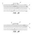
- FIG. 1illustrates a plurality of conventional magnetic memory cells 10 formed on a metal conducting line 12 , preferably copper or aluminum, which is deposited on a substrate (not shown).
- the conducting line 12extends to the right and to the left of the page.
- the memory cells 10can be formed by first depositing a pinned layer 14 on the conducting line 12 , depositing an insulating barrier layer 16 over the pinned layer 14 , and depositing a sense layer 18 over the barrier layer 16 .
- the pinned layer 14 , barrier layer 16 , and sense layer 18can then be patterned and etched to form the memory cells 10 using methods that are well-known to those of skill in the art.
- the pinned layer 14may comprise a stack of magnetic and associated adjacent sublayers.
- the pinned layer 14may comprise a tantalum seed sublayer, a nickel-iron seed sublayer, a magnesium oxide, iridium-manganese, platinum-manganese or nickel-manganese pinning sublayer, and a nickel-iron, nickel-iron-cobalt, cobalt-iron or nickel-iron-chromium sublayer.
- the baffler layer 16is preferably thin enough to allow the tunneling of electrons from the sense layer 18 to the pinned layer 14 .
- the barrier layer 16may comprise, for example, aluminum oxide, having a thickness within the range of about 0.5 nm to about 3 nm, preferably within the range of about 1 nm to about 2 nm.
- the sense layer 18may comprise a stack of magnetic and associated adjacent blanket sublayers.
- the sense layer 18may comprise a tantalum sublayer, a tungsten nitride sublayer, and a nickel-iron, nickel-iron-cobalt, cobalt-iron, cobalt or copper sublayer.
- This coating of conductive material 20may comprise, for example, particles of the pinned layer 14 that are thrown up along the sidewalls of the memory cell 10 during the process of etching through the pinned layer 14 , particularly if an etching process with a physical component is used, such as an ion milling process or a reactive ion etch.
- the thin coating of conductive material 20 along the sidewalls of the memory cell 10is undesirable because it can create a conductive path between the pinned layer 14 and the sense layer 18 . Such a conductive path creates an electrical short across the barrier layer 16 that can prevent the memory cell 10 from functioning properly. Therefore, the coating of conductive material 20 along the sidewalls of the memory cells 10 can undesirably reduce the yield of the manufacturing process. Although an additional cleaning step can be performed to remove the coating of conductive material 20 from the sidewalls of the memory cells 10 , such an additional step can add cost to the manufacturing process and can also have a harmful effect on the remaining structures.
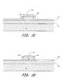
- FIG. 2illustrates a plurality of magnetic memory cells 10 with spacers 22 adjacent to the sense layers 18 .
- the spacers 22preferably comprise a nonconductive material, such as, for example, silicon nitride, diamond-like carbon, silicon carbide, or an oxide such as silicon oxide or aluminum oxide.
- the spacers 22can be formed using a variety of well-known techniques. For example, the sense layer 18 can be patterned and etched with a hard or resist mask in place, followed by the deposition of a blanket layer of nonconductive material. The resulting structure can then be subjected to a spacer etch, followed by etching through the underlying pinned layer 14 .
- the spacers 22advantageously reduce the likelihood that such a coating will form a conductive path between the sense layer 18 and the pinned layer 14 of a given memory cell 10 by largely protecting the sense layer 18 during etching of the pinned layers 14 . Therefore, the spacers 22 can advantageously reduce the number of memory cells 10 that short out, thereby increasing the yield of the manufacturing process. Even in a memory cell 10 having a spacer 22 adjacent to the sense layer 18 , however, an electrical short across the barrier layer 16 can still occur due to, inter alia, a small point of contact 24 between the coating of conductive material 20 and the sense layer 18 .
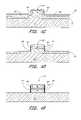
- FIGS. 3A–3Gillustrate a process for forming a magnetic memory cell 10 in accordance with one embodiment of the invention.
- the memory cell 10 of the illustrated embodimentcomprises a TMR magnetic memory cell having a particular configuration
- the memory cell 10could have a wide variety of alternative configurations.
- the pinned layer 14is the bottom layer of the memory cell 10 .
- the pinned layer 14may be the top layer of the memory cell 10 .
- the process of the illustrated embodimentbegins by depositing a pinned layer 14 , a barrier layer 16 , and a sense layer 18 on a conductive line 12 .
- the pinned layer 14may comprise a stack of magnetic and associated adjacent sublayers
- the barrier layer 16preferably comprises a nonconductive material through which electron tunneling can occur
- the sense layer 18may comprise a stack of magnetic and associated adjacent sublayers.
- both the pinned layer 14 and the sense layer 18comprise a ferromagnetic material that is an alloy of any of several metals, such as, for example, iron, nickel, and/or cobalt having a thickness preferably within the range of about 1 nm to about 30 nm, more preferably within the range of about 2.5 nm to about 20 nm, and still more preferably within the range of about 5 nm to about 10 nm.
- the barrier layer 16comprises an oxide of a metal, such as, for example, aluminum oxide, having a thickness preferably within the range of about 0.5 nm to about 3 nm, more preferably within the range of about 1 nm to about 2 ⁇ m.
- a metalsuch as, for example, aluminum oxide
- a hard mask 30can be deposited as a blanket layer over the sense layer 18 , and then patterned and etched using a variety of conventional materials and methods.
- the hard mask 30may comprise Si 3 N 4 , SiO 3 N 4 , SiC, or any other suitable hard mask material, having a thickness preferably within the range of about 100 ⁇ to about 5000 ⁇ , more preferably within the range of about 500 ⁇ to about 2000 ⁇ .
- the hard mask 30can be patterned using a number of well-known techniques, such as, for example, conventional photolithography and etching processes.
- the sense layer 18is etched in the areas that are not covered by the hard mask 30 .
- This etchcan be performed using a variety of well-known processes, such as, for example, ion milling, reactive ion etching, or chemical etching. If a process involving a chemical etchant is selected, any of a number of well-known etchants can be used, such as, for example, CO 2 —NH 3 or CO—NH 3 .
- the etching of the sense layer 18preferably stops at the barrier layer 16 .
- the hard mask 30is also partially etched during the etching of the sense layer 18 .
- the resulting structurecan be optionally oxidized to transform the outer portions of the sense layer 18 into a nonconductive material (not shown).
- This optional oxidation stepcan be performed using an oxidant such as, for example, O 3 , at a flow rate preferably within the range of about 1 sccm to about 1000 sccm, more preferably within the range of about 100 sccm to about 500 sccm.
- this optional oxidation stepinvolves using O 2 as an oxidant during a plasma oxidation process. Because this optional oxidation step reduces the amount of conductive surface area around the sides of the sense layer 18 , it advantageously reduces the likelihood of a conductive path forming between the pinned layer 14 and the sense layer 18 .
- the spacer material 22can be any suitable material (e.g., Si 3 N 4 ) but preferably comprises a low k electrical insulator, with k value preferably less than 3.5, more preferably less than 3.0.
- k valuepreferably less than 3.5, more preferably less than 3.0.
- materialsexist that can be used as the spacer material 22 , such as, for example, silicon nitride, diamond-like carbon, silicon carbide, or an oxide such as silicon oxide or aluminum oxide.
- the spacer material 22can be deposited using any suitable process, such as, for example, physical vapor deposition or chemical vapor deposition.
- the thickness of the layer of spacer material 22preferably falls within the range of about 5 nm to about 100 nm, and more preferably within the range of about 20 nm to about 40 nm.
- the layer of spacer material 22is etched, preferably using an anisotropic etch process that preferentially etches the horizontal portions of the layer of spacer material 22 relative to the vertical portions of the layer of spacer material 22 . Therefore, an etching process with a physical component is preferably used, such as an ion milling process or a reactive ion etch. In some embodiments, for example, a reactive ion etch is used with an appropriate etchant for the selected spacer material 22 .
- the spacer material 22comprises silicon nitride and the etchant comprises CF 4 or CHF 3 .
- the spacer material 22comprises diamond-like carbon and the etchant comprises oxygen-based plasma. In other exemplary embodiments, the spacer material 22 comprises silicon carbide and the etchant comprises CF 4 , CH 2 F 2 , or C 2 F 6 .
- the spacer etch processstops at the barrier layer 16 . In other embodiments, the spacer etch process continues until the pinned layer 14 is reached. In these embodiments, the barrier layer 16 is also etched as part of the same process that etches the layer of spacer material 22 .
- the remaining layersare etched.
- the process used to etch the remaining layersis substantially similar to the process used to etch the sense layer 18 .
- This processmay comprise, for example, ion milling, reactive ion etching, or chemical etching, and may use an etchant such as, for example, CO 2 —NH 3 or CO—NH 3 .
- the hard mask 30is also partially etched during the etching of the pinned layer 14 .
- a thin coating of conductive material 20may form along the sidewalls of the memory cell 10 .
- the thin coating of conductive material 20may comprise particles of the pinned layer 14 that are thrown up as byproducts of the etching process of the pinned layer 14 .
- the thin coating of conductive material 20may form a conductive path between the pinned layer 14 and the sense layer 18 , thereby creating an electrical short across the barrier layer 16 that can cause the memory cell 10 to malfunction.
- the spacers 22minimize the amount of exposed conductive surface area around the sides of the sense layer 18 , and thus reduce the likelihood of a conductive path forming between the pinned layer 14 and the sense layer 18 , such a conductive path can still exist if there is even only a small point of contact 24 between the thin coating of conductive material 20 and the sense layer 18 .
- the thin coating of conductive material 20can be oxidized to transform the conductive material 20 into a nonconductive material 36 , as illustrated in FIG. 3F .
- This oxidation stepcan be performed using an oxidant such as, for example, O 3 , at a flow rate preferably within the range of about 1 sccm to about 1000 sccm, more preferably within the range of about 100 sccm to about 500 sccm.
- this oxidation stepinvolves using O 2 as an oxidant during a plasma oxidation process.
- the thin coating of nonconductive material 36is illustrated as one continuous layer in FIGS. 3E–3F , it may be formed as a discontinuous layer.
- the remaining portion of the hard mask 30is removed to complete the process of forming the memory cell 10 .
- the conductive material 20By oxidizing the conductive material 20 , thereby transforming it into a nonconductive material 36 , the likelihood of a conductive path forming between the pinned layer 14 and the sense layer 18 due to a small point of contact 24 between the layer of nonconductive material 36 and the sense layer 18 is substantially reduced. Accordingly, the number of memory cells 10 within an MRAM array that malfunction due to electrical shorts is reduced, and the yield of the manufacturing process for the MRAM device is advantageously improved.
- FIGS. 4A–4Gillustrate an alternative process for forming a magnetic memory cell 10 in accordance with one embodiment of the invention, which is somewhat similar to the embodiment of the invention described above.
- the processbegins with the same steps described above in connection with FIGS. 3A–3B .
- the resulting structureis repeatedly subjected to alternating partial oxidation and partial etch steps until the memory cell 10 is formed.
- the partial oxidation stepsare performed by subjecting the structure to plasma oxidation using a process that is substantially similar to the optional oxidation step described above in connection with FIG. 3B .
- FIG. 4Cwhen the structure is subjected to plasma oxidation, the outer or sidewall portions 40 of the sense layer 18 and the upper portion 42 of the pinned layer 14 are transformed into a nonconductive material, except for the portions that are protected under the hard mask 30 .
- the pinned layer 14can then be partially etched because, even if particles from the upper portion of the pinned layer 14 are deposited along the sidewalls of the structure as byproducts of the etching process, the particles are nonconductive and thus unlikely to cause an electrical short across the barrier layer 16 .
- the grown sidewall spacer in the form of outer portions 40further reduces the likelihood of a short forming across the barrier layer 16 .
- an etching process with a physical componentis preferably used, such as an ion milling process or a reactive ion etch. The partial etch preferably stops before the portion of the pinned layer 14 below the upper portion 42 is reached, such that only nonconductive particles tend to be thrown up along the sidewalls of the memory cell 10 as byproducts of the etching process.
- the steps illustrated in FIGS. 4C–4Dcan be repeated cyclically until the entire pinned layer 14 has been oxidized and etched. In a preferred embodiment, both the oxidation and the etching steps can be performed in situ within the same tool. Then, as illustrated in FIG. 4E , the remaining portion of the hard mask 30 can be removed to complete the process of forming the memory cell 10 .
- the likelihood of a conductive path forming between the pinned layer 14 and the sense layer 18is substantially reduced. Accordingly, the number of memory cells 10 within an MRAM array that malfunction due to electrical shorts is reduced, and the yield of the manufacturing process for the MRAM device is advantageously improved.
- the process illustrated in FIGS. 4A–4Eis advantageously self-aligning because the region under the hard mask 30 is protected from both oxidation and etching. Therefore, although the process involves repeating a series of alternating oxidation and etching steps, the process involves only a single masking step. Because no additional masks are needed to perform the alternating oxidation and etching steps, the process can advantageously be performed at a relatively low cost.
Landscapes
- Engineering & Computer Science (AREA)
- Manufacturing & Machinery (AREA)
- Mram Or Spin Memory Techniques (AREA)
- Hall/Mr Elements (AREA)
Abstract
Description
Claims (36)
Priority Applications (3)
| Application Number | Priority Date | Filing Date | Title |
|---|---|---|---|
| US10/684,967US7112454B2 (en) | 2003-10-14 | 2003-10-14 | System and method for reducing shorting in memory cells |
| US11/412,582US7358553B2 (en) | 2003-10-14 | 2006-04-27 | System and method for reducing shorting in memory cells |
| US11/535,456US7855085B2 (en) | 2003-10-14 | 2006-09-26 | System and method for reducing shorting in memory cells |
Applications Claiming Priority (1)
| Application Number | Priority Date | Filing Date | Title |
|---|---|---|---|
| US10/684,967US7112454B2 (en) | 2003-10-14 | 2003-10-14 | System and method for reducing shorting in memory cells |
Related Child Applications (2)
| Application Number | Title | Priority Date | Filing Date |
|---|---|---|---|
| US11/412,582DivisionUS7358553B2 (en) | 2003-10-14 | 2006-04-27 | System and method for reducing shorting in memory cells |
| US11/535,456ContinuationUS7855085B2 (en) | 2003-10-14 | 2006-09-26 | System and method for reducing shorting in memory cells |
Publications (2)
| Publication Number | Publication Date |
|---|---|
| US20050079638A1 US20050079638A1 (en) | 2005-04-14 |
| US7112454B2true US7112454B2 (en) | 2006-09-26 |
Family
ID=34423062
Family Applications (3)
| Application Number | Title | Priority Date | Filing Date |
|---|---|---|---|
| US10/684,967Expired - LifetimeUS7112454B2 (en) | 2003-10-14 | 2003-10-14 | System and method for reducing shorting in memory cells |
| US11/412,582Expired - LifetimeUS7358553B2 (en) | 2003-10-14 | 2006-04-27 | System and method for reducing shorting in memory cells |
| US11/535,456Active2026-04-08US7855085B2 (en) | 2003-10-14 | 2006-09-26 | System and method for reducing shorting in memory cells |
Family Applications After (2)
| Application Number | Title | Priority Date | Filing Date |
|---|---|---|---|
| US11/412,582Expired - LifetimeUS7358553B2 (en) | 2003-10-14 | 2006-04-27 | System and method for reducing shorting in memory cells |
| US11/535,456Active2026-04-08US7855085B2 (en) | 2003-10-14 | 2006-09-26 | System and method for reducing shorting in memory cells |
Country Status (1)
| Country | Link |
|---|---|
| US (3) | US7112454B2 (en) |
Cited By (8)
| Publication number | Priority date | Publication date | Assignee | Title |
|---|---|---|---|---|
| US20070020775A1 (en)* | 2003-10-14 | 2007-01-25 | Micron Technology, Inc. | System and method for reducing shorting in memory cells |
| US8123968B2 (en) | 2005-08-25 | 2012-02-28 | Round Rock Research, Llc | Multiple deposition for integration of spacers in pitch multiplication process |
| US8216949B2 (en)* | 2004-09-02 | 2012-07-10 | Round Rock Research, Llc | Method for integrated circuit fabrication using pitch multiplication |
| KR20130015564A (en)* | 2011-08-04 | 2013-02-14 | 에스케이하이닉스 주식회사 | Method for fabricating magnetic tunnel junction device |
| US8615868B2 (en) | 2011-11-29 | 2013-12-31 | HGST Netherlands B.V. | Method for manufacturing a magnetic sensor using two step ion milling |
| US9349939B2 (en)* | 2014-05-23 | 2016-05-24 | Qualcomm Incorporated | Etch-resistant protective coating for a magnetic tunnel junction device |
| US10515801B2 (en) | 2007-06-04 | 2019-12-24 | Micron Technology, Inc. | Pitch multiplication using self-assembling materials |
| US11302630B2 (en)* | 2020-04-08 | 2022-04-12 | International Business Machines Corporation | Electrode-via structure |
Families Citing this family (19)
| Publication number | Priority date | Publication date | Assignee | Title |
|---|---|---|---|---|
| US6724652B2 (en)* | 2002-05-02 | 2004-04-20 | Micron Technology, Inc. | Low remanence flux concentrator for MRAM devices |
| US7002228B2 (en) | 2003-02-18 | 2006-02-21 | Micron Technology, Inc. | Diffusion barrier for improving the thermal stability of MRAM devices |
| US7531367B2 (en)* | 2006-01-18 | 2009-05-12 | International Business Machines Corporation | Utilizing sidewall spacer features to form magnetic tunnel junctions in an integrated circuit |
| US8043732B2 (en) | 2008-11-11 | 2011-10-25 | Seagate Technology Llc | Memory cell with radial barrier |
| KR101527533B1 (en)* | 2009-01-09 | 2015-06-10 | 삼성전자주식회사 | Method of forming magnetic memory device |
| KR20120058113A (en)* | 2010-11-29 | 2012-06-07 | 삼성전자주식회사 | Method for forming magnetic tunnel junction structure and method for forming magnetic random access memory using the same |
| US8976569B2 (en) | 2013-01-30 | 2015-03-10 | Hewlett-Packard Development Company, L.P. | Mitigation of inoperable low resistance elements in programable crossbar arrays |
| EP2973726A4 (en)* | 2013-03-11 | 2016-11-30 | Crocus Technology Inc | Magnetic random access memory cells with isolating liners |
| CN105814679A (en) | 2013-06-28 | 2016-07-27 | 英特尔公司 | Preservation of fine pitch redistribution lines |
| KR102082322B1 (en) | 2013-08-09 | 2020-02-27 | 삼성전자주식회사 | Method of forming magnetic memory devices |
| EP3123476B1 (en) | 2014-03-28 | 2019-10-16 | Intel Corporation | Techniques for forming spin-transfer-torque memory having a dot-contacted free magnetic layer |
| US10438997B2 (en) | 2014-05-21 | 2019-10-08 | Avalanche Technology, Inc. | Multilayered seed structure for magnetic memory element including a CoFeB seed layer |
| US10347691B2 (en) | 2014-05-21 | 2019-07-09 | Avalanche Technology, Inc. | Magnetic memory element with multilayered seed structure |
| US10050083B2 (en) | 2014-05-21 | 2018-08-14 | Avalanche Technology, Inc. | Magnetic structure with multilayered seed |
| US9496489B2 (en) | 2014-05-21 | 2016-11-15 | Avalanche Technology, Inc. | Magnetic random access memory with multilayered seed structure |
| EP3673522B1 (en) | 2017-08-23 | 2022-10-05 | Everspin Technologies, Inc. | Magnetoresistive bit fabrication by multi-step etching |
| CN109560102A (en)* | 2017-09-26 | 2019-04-02 | 中电海康集团有限公司 | MRAM and its production method |
| CN109378386B (en)* | 2018-10-16 | 2022-06-07 | 南京邮电大学 | Method for regulating the morphology of lead-free perovskite solar cells and prepared battery devices |
| US11849644B2 (en)* | 2021-04-15 | 2023-12-19 | Taiwan Semiconductor Manufacturing Company, Ltd. | Method of fabricating magneto-resistive random access memory (MRAM) |
Citations (55)
| Publication number | Priority date | Publication date | Assignee | Title |
|---|---|---|---|---|
| US3623032A (en) | 1970-02-16 | 1971-11-23 | Honeywell Inc | Keeper configuration for a thin-film memory |
| US3623035A (en) | 1968-02-02 | 1971-11-23 | Fuji Electric Co Ltd | Magnetic memory matrix and process for its production |
| US3816909A (en) | 1969-04-30 | 1974-06-18 | Hitachi Chemical Co Ltd | Method of making a wire memory plane |
| US3947831A (en) | 1972-12-11 | 1976-03-30 | Kokusai Denshin Denwa Kabushiki Kaisha | Word arrangement matrix memory of high bit density having a magnetic flux keeper |
| US4044330A (en) | 1976-03-30 | 1977-08-23 | Honeywell Information Systems, Inc. | Power strobing to achieve a tri state |
| US4060794A (en) | 1976-03-31 | 1977-11-29 | Honeywell Information Systems Inc. | Apparatus and method for generating timing signals for latched type memories |
| US4158891A (en) | 1975-08-18 | 1979-06-19 | Honeywell Information Systems Inc. | Transparent tri state latch |
| US4455626A (en) | 1983-03-21 | 1984-06-19 | Honeywell Inc. | Thin film memory with magnetoresistive read-out |
| US4731757A (en) | 1986-06-27 | 1988-03-15 | Honeywell Inc. | Magnetoresistive memory including thin film storage cells having tapered ends |
| US4780848A (en) | 1986-06-03 | 1988-10-25 | Honeywell Inc. | Magnetoresistive memory with multi-layer storage cells having layers of limited thickness |
| US4801883A (en) | 1986-06-02 | 1989-01-31 | The Regents Of The University Of California | Integrated-circuit one-way isolation coupler incorporating one or several carrier-domain magnetometers |
| US4945397A (en) | 1986-12-08 | 1990-07-31 | Honeywell Inc. | Resistive overlayer for magnetic films |
| US5039655A (en) | 1989-07-28 | 1991-08-13 | Ampex Corporation | Thin film memory device having superconductor keeper for eliminating magnetic domain creep |
| US5064499A (en) | 1990-04-09 | 1991-11-12 | Honeywell Inc. | Inductively sensed magnetic memory manufacturing method |
| US5140549A (en) | 1990-04-09 | 1992-08-18 | Honeywell Inc. | Inductively sensed magnetic memory |
| US5496759A (en) | 1994-12-29 | 1996-03-05 | Honeywell Inc. | Highly producible magnetoresistive RAM process |
| US5547599A (en) | 1989-03-17 | 1996-08-20 | Raytheon Company | Ferrite/epoxy film |
| US5569617A (en) | 1995-12-21 | 1996-10-29 | Honeywell Inc. | Method of making integrated spacer for magnetoresistive RAM |
| US5587943A (en) | 1995-02-13 | 1996-12-24 | Integrated Microtransducer Electronics Corporation | Nonvolatile magnetoresistive memory with fully closed flux operation |
| EP0776011A2 (en) | 1995-11-24 | 1997-05-28 | Motorola, Inc. | Magnetic memory and method therefor |
| US5650958A (en) | 1996-03-18 | 1997-07-22 | International Business Machines Corporation | Magnetic tunnel junctions with controlled magnetic response |
| US5701222A (en) | 1995-09-11 | 1997-12-23 | International Business Machines Corporation | Spin valve sensor with antiparallel magnetization of pinned layers |
| US5726498A (en) | 1995-05-26 | 1998-03-10 | International Business Machines Corporation | Wire shape conferring reduced crosstalk and formation methods |
| US5741435A (en) | 1995-08-08 | 1998-04-21 | Nano Systems, Inc. | Magnetic memory having shape anisotropic magnetic elements |
| WO1998020496A1 (en) | 1996-11-08 | 1998-05-14 | Nonvolatile Electronics, Incorporated | Spin dependent tunneling memory |
| US5756366A (en) | 1995-12-21 | 1998-05-26 | Honeywell Inc. | Magnetic hardening of bit edges of magnetoresistive RAM |
| US5795823A (en) | 1995-06-07 | 1998-08-18 | Advanced Micro Devices, Inc. | Self aligned via dual damascene |
| US5804458A (en)* | 1996-12-16 | 1998-09-08 | Motorola, Inc. | Method of fabricating spaced apart submicron magnetic memory cells |
| US5861328A (en) | 1996-10-07 | 1999-01-19 | Motorola, Inc. | Method of fabricating GMR devices |
| US5926394A (en) | 1996-09-30 | 1999-07-20 | Intel Corporation | Method and apparatus for regulating the voltage supplied to an integrated circuit |
| US5956267A (en) | 1997-12-18 | 1999-09-21 | Honeywell Inc | Self-aligned wordline keeper and method of manufacture therefor |
| US5982658A (en) | 1997-10-31 | 1999-11-09 | Honeywell Inc. | MRAM design to reduce dissimilar nearest neighbor effects |
| JP2000030222A (en) | 1998-07-08 | 2000-01-28 | Fujitsu Ltd | Magnetic sensor |
| US6028786A (en) | 1997-04-28 | 2000-02-22 | Canon Kabushiki Kaisha | Magnetic memory element having coupled magnetic layers forming closed magnetic circuit |
| DE19836567A1 (en) | 1998-08-12 | 2000-02-24 | Siemens Ag | Memory cell structure with magneto-resistive memory elements comprises a magnetizable yoke surrounding one of the intersecting lines at a memory element location |
| WO2000019440A2 (en) | 1998-09-30 | 2000-04-06 | Infineon Technologies Ag | Magnetoresistive memory with low current density |
| US6048739A (en) | 1997-12-18 | 2000-04-11 | Honeywell Inc. | Method of manufacturing a high density magnetic memory device |
| US6136705A (en) | 1998-10-22 | 2000-10-24 | National Semiconductor Corporation | Self-aligned dual thickness cobalt silicide layer formation process |
| US6153443A (en) | 1998-12-21 | 2000-11-28 | Motorola, Inc. | Method of fabricating a magnetic random access memory |
| US6174737B1 (en) | 1998-08-31 | 2001-01-16 | Motorola, Inc. | Magnetic random access memory and fabricating method thereof |
| US6218302B1 (en) | 1998-07-21 | 2001-04-17 | Motorola Inc. | Method for forming a semiconductor device |
| US6338899B1 (en) | 1998-06-30 | 2002-01-15 | Kabushiki Kaisha Toshiba | Magnetoresistance effect element, magnetic head, magnetic head assembly, magnetic storage system |
| US6358756B1 (en) | 2001-02-07 | 2002-03-19 | Micron Technology, Inc. | Self-aligned, magnetoresistive random-access memory (MRAM) structure utilizing a spacer containment scheme |
| US20020041514A1 (en) | 1999-02-26 | 2002-04-11 | Ulrich Scheler | Memory cell configuration and method for its production |
| US6379978B2 (en) | 1998-07-15 | 2002-04-30 | Infineon Technologies Ag | Memory cell configuration in which an electrical resistance of a memory element represents an information item and can be influenced by a magnetic field, and method for fabricating it |
| US6392922B1 (en) | 2000-08-14 | 2002-05-21 | Micron Technology, Inc. | Passivated magneto-resistive bit structure and passivation method therefor |
| US6391658B1 (en) | 1999-10-26 | 2002-05-21 | International Business Machines Corporation | Formation of arrays of microelectronic elements |
| US20020076572A1 (en)* | 2000-09-29 | 2002-06-20 | Manfred Engelhardt | Method for fabricating integrated circuit arrangements, and associated circuit arrangements, in particular tunnel contact elements |
| US6440753B1 (en) | 2001-01-24 | 2002-08-27 | Infineon Technologies North America Corp. | Metal hard mask for ILD RIE processing of semiconductor memory devices to prevent oxidation of conductive lines |
| US6485989B1 (en) | 2001-08-30 | 2002-11-26 | Micron Technology, Inc. | MRAM sense layer isolation |
| US6627913B2 (en)* | 2001-09-10 | 2003-09-30 | Micron Technology, Inc. | Insulation of an MRAM device through a self-aligned spacer |
| US6770491B2 (en) | 2002-08-07 | 2004-08-03 | Micron Technology, Inc. | Magnetoresistive memory and method of manufacturing the same |
| US6783995B2 (en) | 2002-04-30 | 2004-08-31 | Micron Technology, Inc. | Protective layers for MRAM devices |
| US6855563B2 (en)* | 2002-05-01 | 2005-02-15 | Sony Corporation | Method of manufacturing a tunnel magneto-resistance based magnetic memory device |
| US6911156B2 (en)* | 2003-04-16 | 2005-06-28 | Freescale Semiconductor, Inc. | Methods for fabricating MRAM device structures |
Family Cites Families (13)
| Publication number | Priority date | Publication date | Assignee | Title |
|---|---|---|---|---|
| JP3350955B2 (en)* | 1992-05-18 | 2002-11-25 | 株式会社日立製作所 | Method for repairing semiconductor device |
| US5569619A (en)* | 1992-06-24 | 1996-10-29 | Lg Semicon Co., Ltd. | Method for forming a capacitor of a semiconductor memory cell |
| KR100378414B1 (en)* | 1999-05-31 | 2003-03-29 | 닛뽕덴끼 가부시끼가이샤 | Magnetoresistance effect element and manufacturing method thereof, and magnetic storage device using the same |
| JP2001196659A (en)* | 2000-01-12 | 2001-07-19 | Tdk Corp | Tunnel magnetoresistive effect element, thin magnetic film head, memory element, and manufacturing method for them |
| JP5013494B2 (en)* | 2001-04-06 | 2012-08-29 | ルネサスエレクトロニクス株式会社 | Manufacturing method of magnetic memory |
| KR100445064B1 (en)* | 2001-06-30 | 2004-08-21 | 주식회사 하이닉스반도체 | Method for fabrication of magnetic random access memory |
| US6759263B2 (en)* | 2002-08-29 | 2004-07-06 | Chentsau Ying | Method of patterning a layer of magnetic material |
| JP4008857B2 (en)* | 2003-03-24 | 2007-11-14 | 株式会社東芝 | Semiconductor memory device and manufacturing method thereof |
| KR100500455B1 (en)* | 2003-08-11 | 2005-07-18 | 삼성전자주식회사 | Magnetic tunnel junction structure having a oxidized buffer layer and method of fabricating the same |
| JP2005079258A (en)* | 2003-08-29 | 2005-03-24 | Canon Inc | Magnetic etching method, magnetoresistive effect film, and magnetic random access memory |
| US6984529B2 (en)* | 2003-09-10 | 2006-01-10 | Infineon Technologies Ag | Fabrication process for a magnetic tunnel junction device |
| US7112454B2 (en) | 2003-10-14 | 2006-09-26 | Micron Technology, Inc. | System and method for reducing shorting in memory cells |
| US7205164B1 (en)* | 2005-01-19 | 2007-04-17 | Silicon Magnetic Systems | Methods for fabricating magnetic cell junctions and a structure resulting and/or used for such methods |
- 2003
- 2003-10-14USUS10/684,967patent/US7112454B2/ennot_activeExpired - Lifetime
- 2006
- 2006-04-27USUS11/412,582patent/US7358553B2/ennot_activeExpired - Lifetime
- 2006-09-26USUS11/535,456patent/US7855085B2/enactiveActive
Patent Citations (56)
| Publication number | Priority date | Publication date | Assignee | Title |
|---|---|---|---|---|
| US3623035A (en) | 1968-02-02 | 1971-11-23 | Fuji Electric Co Ltd | Magnetic memory matrix and process for its production |
| US3816909A (en) | 1969-04-30 | 1974-06-18 | Hitachi Chemical Co Ltd | Method of making a wire memory plane |
| US3623032A (en) | 1970-02-16 | 1971-11-23 | Honeywell Inc | Keeper configuration for a thin-film memory |
| US3947831A (en) | 1972-12-11 | 1976-03-30 | Kokusai Denshin Denwa Kabushiki Kaisha | Word arrangement matrix memory of high bit density having a magnetic flux keeper |
| US4158891A (en) | 1975-08-18 | 1979-06-19 | Honeywell Information Systems Inc. | Transparent tri state latch |
| US4044330A (en) | 1976-03-30 | 1977-08-23 | Honeywell Information Systems, Inc. | Power strobing to achieve a tri state |
| US4060794A (en) | 1976-03-31 | 1977-11-29 | Honeywell Information Systems Inc. | Apparatus and method for generating timing signals for latched type memories |
| US4455626A (en) | 1983-03-21 | 1984-06-19 | Honeywell Inc. | Thin film memory with magnetoresistive read-out |
| US4801883A (en) | 1986-06-02 | 1989-01-31 | The Regents Of The University Of California | Integrated-circuit one-way isolation coupler incorporating one or several carrier-domain magnetometers |
| US4849695A (en) | 1986-06-02 | 1989-07-18 | University Of California | Null-detection magnetometers |
| US4780848A (en) | 1986-06-03 | 1988-10-25 | Honeywell Inc. | Magnetoresistive memory with multi-layer storage cells having layers of limited thickness |
| US4731757A (en) | 1986-06-27 | 1988-03-15 | Honeywell Inc. | Magnetoresistive memory including thin film storage cells having tapered ends |
| US4945397A (en) | 1986-12-08 | 1990-07-31 | Honeywell Inc. | Resistive overlayer for magnetic films |
| US5547599A (en) | 1989-03-17 | 1996-08-20 | Raytheon Company | Ferrite/epoxy film |
| US5039655A (en) | 1989-07-28 | 1991-08-13 | Ampex Corporation | Thin film memory device having superconductor keeper for eliminating magnetic domain creep |
| US5064499A (en) | 1990-04-09 | 1991-11-12 | Honeywell Inc. | Inductively sensed magnetic memory manufacturing method |
| US5140549A (en) | 1990-04-09 | 1992-08-18 | Honeywell Inc. | Inductively sensed magnetic memory |
| US5496759A (en) | 1994-12-29 | 1996-03-05 | Honeywell Inc. | Highly producible magnetoresistive RAM process |
| US5587943A (en) | 1995-02-13 | 1996-12-24 | Integrated Microtransducer Electronics Corporation | Nonvolatile magnetoresistive memory with fully closed flux operation |
| US5726498A (en) | 1995-05-26 | 1998-03-10 | International Business Machines Corporation | Wire shape conferring reduced crosstalk and formation methods |
| US5795823A (en) | 1995-06-07 | 1998-08-18 | Advanced Micro Devices, Inc. | Self aligned via dual damascene |
| US5741435A (en) | 1995-08-08 | 1998-04-21 | Nano Systems, Inc. | Magnetic memory having shape anisotropic magnetic elements |
| US5701222A (en) | 1995-09-11 | 1997-12-23 | International Business Machines Corporation | Spin valve sensor with antiparallel magnetization of pinned layers |
| EP0776011A2 (en) | 1995-11-24 | 1997-05-28 | Motorola, Inc. | Magnetic memory and method therefor |
| US5569617A (en) | 1995-12-21 | 1996-10-29 | Honeywell Inc. | Method of making integrated spacer for magnetoresistive RAM |
| US5756366A (en) | 1995-12-21 | 1998-05-26 | Honeywell Inc. | Magnetic hardening of bit edges of magnetoresistive RAM |
| US5650958A (en) | 1996-03-18 | 1997-07-22 | International Business Machines Corporation | Magnetic tunnel junctions with controlled magnetic response |
| US5926394A (en) | 1996-09-30 | 1999-07-20 | Intel Corporation | Method and apparatus for regulating the voltage supplied to an integrated circuit |
| US5861328A (en) | 1996-10-07 | 1999-01-19 | Motorola, Inc. | Method of fabricating GMR devices |
| WO1998020496A1 (en) | 1996-11-08 | 1998-05-14 | Nonvolatile Electronics, Incorporated | Spin dependent tunneling memory |
| US5804458A (en)* | 1996-12-16 | 1998-09-08 | Motorola, Inc. | Method of fabricating spaced apart submicron magnetic memory cells |
| US6028786A (en) | 1997-04-28 | 2000-02-22 | Canon Kabushiki Kaisha | Magnetic memory element having coupled magnetic layers forming closed magnetic circuit |
| US5982658A (en) | 1997-10-31 | 1999-11-09 | Honeywell Inc. | MRAM design to reduce dissimilar nearest neighbor effects |
| US5956267A (en) | 1997-12-18 | 1999-09-21 | Honeywell Inc | Self-aligned wordline keeper and method of manufacture therefor |
| US6048739A (en) | 1997-12-18 | 2000-04-11 | Honeywell Inc. | Method of manufacturing a high density magnetic memory device |
| US6338899B1 (en) | 1998-06-30 | 2002-01-15 | Kabushiki Kaisha Toshiba | Magnetoresistance effect element, magnetic head, magnetic head assembly, magnetic storage system |
| JP2000030222A (en) | 1998-07-08 | 2000-01-28 | Fujitsu Ltd | Magnetic sensor |
| US6379978B2 (en) | 1998-07-15 | 2002-04-30 | Infineon Technologies Ag | Memory cell configuration in which an electrical resistance of a memory element represents an information item and can be influenced by a magnetic field, and method for fabricating it |
| US6218302B1 (en) | 1998-07-21 | 2001-04-17 | Motorola Inc. | Method for forming a semiconductor device |
| DE19836567A1 (en) | 1998-08-12 | 2000-02-24 | Siemens Ag | Memory cell structure with magneto-resistive memory elements comprises a magnetizable yoke surrounding one of the intersecting lines at a memory element location |
| US6174737B1 (en) | 1998-08-31 | 2001-01-16 | Motorola, Inc. | Magnetic random access memory and fabricating method thereof |
| WO2000019440A2 (en) | 1998-09-30 | 2000-04-06 | Infineon Technologies Ag | Magnetoresistive memory with low current density |
| US6136705A (en) | 1998-10-22 | 2000-10-24 | National Semiconductor Corporation | Self-aligned dual thickness cobalt silicide layer formation process |
| US6153443A (en) | 1998-12-21 | 2000-11-28 | Motorola, Inc. | Method of fabricating a magnetic random access memory |
| US20020041514A1 (en) | 1999-02-26 | 2002-04-11 | Ulrich Scheler | Memory cell configuration and method for its production |
| US6391658B1 (en) | 1999-10-26 | 2002-05-21 | International Business Machines Corporation | Formation of arrays of microelectronic elements |
| US6392922B1 (en) | 2000-08-14 | 2002-05-21 | Micron Technology, Inc. | Passivated magneto-resistive bit structure and passivation method therefor |
| US20020076572A1 (en)* | 2000-09-29 | 2002-06-20 | Manfred Engelhardt | Method for fabricating integrated circuit arrangements, and associated circuit arrangements, in particular tunnel contact elements |
| US6440753B1 (en) | 2001-01-24 | 2002-08-27 | Infineon Technologies North America Corp. | Metal hard mask for ILD RIE processing of semiconductor memory devices to prevent oxidation of conductive lines |
| US6358756B1 (en) | 2001-02-07 | 2002-03-19 | Micron Technology, Inc. | Self-aligned, magnetoresistive random-access memory (MRAM) structure utilizing a spacer containment scheme |
| US6485989B1 (en) | 2001-08-30 | 2002-11-26 | Micron Technology, Inc. | MRAM sense layer isolation |
| US6627913B2 (en)* | 2001-09-10 | 2003-09-30 | Micron Technology, Inc. | Insulation of an MRAM device through a self-aligned spacer |
| US6783995B2 (en) | 2002-04-30 | 2004-08-31 | Micron Technology, Inc. | Protective layers for MRAM devices |
| US6855563B2 (en)* | 2002-05-01 | 2005-02-15 | Sony Corporation | Method of manufacturing a tunnel magneto-resistance based magnetic memory device |
| US6770491B2 (en) | 2002-08-07 | 2004-08-03 | Micron Technology, Inc. | Magnetoresistive memory and method of manufacturing the same |
| US6911156B2 (en)* | 2003-04-16 | 2005-06-28 | Freescale Semiconductor, Inc. | Methods for fabricating MRAM device structures |
Non-Patent Citations (7)
| Title |
|---|
| Chen et al., "Magnetic tunnel junction pattern technique," Journal of Applied Physics, vol. 93, No. 10, May 15, 2003, pp. 8379-8381. |
| Kula et al., "Development and process control of magnetic tunnel junctions for magnetic random access memory devices," Journal of Applied Physics, vol. 93, No. 10, May 15, 2003, pp. 8373-8375. |
| Pohm et al., "Experimental and Analytical Properties of 0.2 Micron Wide, Multi-Layer, GMR, Memory Elements," IEEE Transactions on Magnetics, vol. 32, No. 5, Sep. 1996, pp. 4645-4647. |
| Pohm et al., "The Architecture of a High Performance Mass Store with GMR Memory Cells," Nonvolatile Electronics, Honeywell Brochure, pp. 1-3. |
| Prinz, Gary A., "Magnetoelectronics," Science, vol. 282, Nov. 27, 1998, pp. 1660-1663. |
| Razavi et al., "Design Techniques for High-Speed, High Resolution Comparators," IEEE Journal of Solid-State Circuits, vol. 27, No. 12, Dec. 1992, pp. 1916-1926. |
| Wang et al., "Feasibility of Ultra-Dense Spin-Tunneling Random Access Memory," IEEE Transactions on Magnetics, vol. 33, No. 6, Nov. 1997, pp. 4498-4512. |
Cited By (11)
| Publication number | Priority date | Publication date | Assignee | Title |
|---|---|---|---|---|
| US20070020775A1 (en)* | 2003-10-14 | 2007-01-25 | Micron Technology, Inc. | System and method for reducing shorting in memory cells |
| US7855085B2 (en) | 2003-10-14 | 2010-12-21 | Micron Technology, Inc. | System and method for reducing shorting in memory cells |
| US8216949B2 (en)* | 2004-09-02 | 2012-07-10 | Round Rock Research, Llc | Method for integrated circuit fabrication using pitch multiplication |
| US8123968B2 (en) | 2005-08-25 | 2012-02-28 | Round Rock Research, Llc | Multiple deposition for integration of spacers in pitch multiplication process |
| US10515801B2 (en) | 2007-06-04 | 2019-12-24 | Micron Technology, Inc. | Pitch multiplication using self-assembling materials |
| KR20130015564A (en)* | 2011-08-04 | 2013-02-14 | 에스케이하이닉스 주식회사 | Method for fabricating magnetic tunnel junction device |
| US8642358B2 (en)* | 2011-08-04 | 2014-02-04 | Hynix Semiconductor Inc. | Method for fabricating magnetic tunnel junction device |
| KR101870873B1 (en)* | 2011-08-04 | 2018-07-20 | 에스케이하이닉스 주식회사 | Method for fabricating magnetic tunnel junction device |
| US8615868B2 (en) | 2011-11-29 | 2013-12-31 | HGST Netherlands B.V. | Method for manufacturing a magnetic sensor using two step ion milling |
| US9349939B2 (en)* | 2014-05-23 | 2016-05-24 | Qualcomm Incorporated | Etch-resistant protective coating for a magnetic tunnel junction device |
| US11302630B2 (en)* | 2020-04-08 | 2022-04-12 | International Business Machines Corporation | Electrode-via structure |
Also Published As
| Publication number | Publication date |
|---|---|
| US20060192235A1 (en) | 2006-08-31 |
| US20050079638A1 (en) | 2005-04-14 |
| US7358553B2 (en) | 2008-04-15 |
| US7855085B2 (en) | 2010-12-21 |
| US20070020775A1 (en) | 2007-01-25 |
Similar Documents
| Publication | Publication Date | Title |
|---|---|---|
| US7855085B2 (en) | System and method for reducing shorting in memory cells | |
| US12369495B2 (en) | Magnetoresistive stack/structure and method of manufacturing same | |
| US10847715B2 (en) | Magnetoresistive device and method of manufacturing same | |
| CN102272964B (en) | Magnetic memory cell with radial barriers | |
| US10483460B2 (en) | Method of manufacturing a magnetoresistive stack/ structure using plurality of encapsulation layers | |
| EP1279176B1 (en) | Magnetic element with insulating veils and fabricating method thereof | |
| US6756239B1 (en) | Method for constructing a magneto-resistive element |
Legal Events
| Date | Code | Title | Description |
|---|---|---|---|
| AS | Assignment | Owner name:MICRON TECHNOLOGY, INC., IDAHO Free format text:ASSIGNMENT OF ASSIGNORS INTEREST;ASSIGNORS:DREWES, JOEL A.;DEAK, JAMES G.;REEL/FRAME:015067/0355;SIGNING DATES FROM 20040205 TO 20040304 | |
| STCF | Information on status: patent grant | Free format text:PATENTED CASE | |
| CC | Certificate of correction | ||
| FEPP | Fee payment procedure | Free format text:PAYER NUMBER DE-ASSIGNED (ORIGINAL EVENT CODE: RMPN); ENTITY STATUS OF PATENT OWNER: LARGE ENTITY Free format text:PAYOR NUMBER ASSIGNED (ORIGINAL EVENT CODE: ASPN); ENTITY STATUS OF PATENT OWNER: LARGE ENTITY | |
| FPAY | Fee payment | Year of fee payment:4 | |
| FEPP | Fee payment procedure | Free format text:PAYOR NUMBER ASSIGNED (ORIGINAL EVENT CODE: ASPN); ENTITY STATUS OF PATENT OWNER: LARGE ENTITY Free format text:PAYER NUMBER DE-ASSIGNED (ORIGINAL EVENT CODE: RMPN); ENTITY STATUS OF PATENT OWNER: LARGE ENTITY | |
| FPAY | Fee payment | Year of fee payment:8 | |
| AS | Assignment | Owner name:U.S. BANK NATIONAL ASSOCIATION, AS COLLATERAL AGENT, CALIFORNIA Free format text:SECURITY INTEREST;ASSIGNOR:MICRON TECHNOLOGY, INC.;REEL/FRAME:038669/0001 Effective date:20160426 Owner name:U.S. BANK NATIONAL ASSOCIATION, AS COLLATERAL AGEN Free format text:SECURITY INTEREST;ASSIGNOR:MICRON TECHNOLOGY, INC.;REEL/FRAME:038669/0001 Effective date:20160426 | |
| AS | Assignment | Owner name:MORGAN STANLEY SENIOR FUNDING, INC., AS COLLATERAL AGENT, MARYLAND Free format text:PATENT SECURITY AGREEMENT;ASSIGNOR:MICRON TECHNOLOGY, INC.;REEL/FRAME:038954/0001 Effective date:20160426 Owner name:MORGAN STANLEY SENIOR FUNDING, INC., AS COLLATERAL Free format text:PATENT SECURITY AGREEMENT;ASSIGNOR:MICRON TECHNOLOGY, INC.;REEL/FRAME:038954/0001 Effective date:20160426 | |
| AS | Assignment | Owner name:U.S. BANK NATIONAL ASSOCIATION, AS COLLATERAL AGENT, CALIFORNIA Free format text:CORRECTIVE ASSIGNMENT TO CORRECT THE REPLACE ERRONEOUSLY FILED PATENT #7358718 WITH THE CORRECT PATENT #7358178 PREVIOUSLY RECORDED ON REEL 038669 FRAME 0001. ASSIGNOR(S) HEREBY CONFIRMS THE SECURITY INTEREST;ASSIGNOR:MICRON TECHNOLOGY, INC.;REEL/FRAME:043079/0001 Effective date:20160426 Owner name:U.S. BANK NATIONAL ASSOCIATION, AS COLLATERAL AGEN Free format text:CORRECTIVE ASSIGNMENT TO CORRECT THE REPLACE ERRONEOUSLY FILED PATENT #7358718 WITH THE CORRECT PATENT #7358178 PREVIOUSLY RECORDED ON REEL 038669 FRAME 0001. ASSIGNOR(S) HEREBY CONFIRMS THE SECURITY INTEREST;ASSIGNOR:MICRON TECHNOLOGY, INC.;REEL/FRAME:043079/0001 Effective date:20160426 | |
| MAFP | Maintenance fee payment | Free format text:PAYMENT OF MAINTENANCE FEE, 12TH YEAR, LARGE ENTITY (ORIGINAL EVENT CODE: M1553) Year of fee payment:12 | |
| AS | Assignment | Owner name:JPMORGAN CHASE BANK, N.A., AS COLLATERAL AGENT, ILLINOIS Free format text:SECURITY INTEREST;ASSIGNORS:MICRON TECHNOLOGY, INC.;MICRON SEMICONDUCTOR PRODUCTS, INC.;REEL/FRAME:047540/0001 Effective date:20180703 Owner name:JPMORGAN CHASE BANK, N.A., AS COLLATERAL AGENT, IL Free format text:SECURITY INTEREST;ASSIGNORS:MICRON TECHNOLOGY, INC.;MICRON SEMICONDUCTOR PRODUCTS, INC.;REEL/FRAME:047540/0001 Effective date:20180703 | |
| AS | Assignment | Owner name:MICRON TECHNOLOGY, INC., IDAHO Free format text:RELEASE BY SECURED PARTY;ASSIGNOR:U.S. BANK NATIONAL ASSOCIATION, AS COLLATERAL AGENT;REEL/FRAME:047243/0001 Effective date:20180629 | |
| AS | Assignment | Owner name:MICRON TECHNOLOGY, INC., IDAHO Free format text:RELEASE BY SECURED PARTY;ASSIGNOR:MORGAN STANLEY SENIOR FUNDING, INC., AS COLLATERAL AGENT;REEL/FRAME:050937/0001 Effective date:20190731 | |
| AS | Assignment | Owner name:MICRON TECHNOLOGY, INC., IDAHO Free format text:RELEASE BY SECURED PARTY;ASSIGNOR:JPMORGAN CHASE BANK, N.A., AS COLLATERAL AGENT;REEL/FRAME:051028/0001 Effective date:20190731 Owner name:MICRON SEMICONDUCTOR PRODUCTS, INC., IDAHO Free format text:RELEASE BY SECURED PARTY;ASSIGNOR:JPMORGAN CHASE BANK, N.A., AS COLLATERAL AGENT;REEL/FRAME:051028/0001 Effective date:20190731 |