US7112048B2 - BOC BGA package for die with I-shaped bond pad layout - Google Patents
BOC BGA package for die with I-shaped bond pad layoutDownload PDFInfo
- Publication number
- US7112048B2 US7112048B2US10/408,990US40899003AUS7112048B2US 7112048 B2US7112048 B2US 7112048B2US 40899003 AUS40899003 AUS 40899003AUS 7112048 B2US7112048 B2US 7112048B2
- Authority
- US
- United States
- Prior art keywords
- die
- mold
- molding
- support substrate
- opening
- Prior art date
- Legal status (The legal status is an assumption and is not a legal conclusion. Google has not performed a legal analysis and makes no representation as to the accuracy of the status listed.)
- Expired - Lifetime, expires
Links
- 239000000758substrateSubstances0.000claimsabstractdescription156
- 239000004065semiconductorSubstances0.000claimsabstractdescription29
- 238000000465mouldingMethods0.000claimsdescription234
- 150000001875compoundsChemical class0.000claimsdescription117
- 230000002093peripheral effectEffects0.000claimsdescription6
- 238000000034methodMethods0.000abstractdescription56
- 230000008569processEffects0.000description18
- 238000005538encapsulationMethods0.000description11
- 229910000679solderInorganic materials0.000description11
- 239000012790adhesive layerSubstances0.000description8
- 238000004519manufacturing processMethods0.000description7
- 238000004806packaging method and processMethods0.000description7
- 239000000853adhesiveSubstances0.000description6
- 230000001070adhesive effectEffects0.000description6
- 239000000463materialSubstances0.000description5
- 238000012545processingMethods0.000description5
- RYGMFSIKBFXOCR-UHFFFAOYSA-NCopperChemical compound[Cu]RYGMFSIKBFXOCR-UHFFFAOYSA-N0.000description3
- 230000000712assemblyEffects0.000description3
- 238000000429assemblyMethods0.000description3
- 239000008393encapsulating agentSubstances0.000description3
- 239000004033plasticSubstances0.000description3
- 239000002390adhesive tapeSubstances0.000description2
- 229910052782aluminiumInorganic materials0.000description2
- XAGFODPZIPBFFR-UHFFFAOYSA-NaluminiumChemical compound[Al]XAGFODPZIPBFFR-UHFFFAOYSA-N0.000description2
- 229910052802copperInorganic materials0.000description2
- 239000010949copperSubstances0.000description2
- 230000000694effectsEffects0.000description2
- 239000010410layerSubstances0.000description2
- 229910052751metalInorganic materials0.000description2
- 239000002184metalSubstances0.000description2
- 229920001187thermosetting polymerPolymers0.000description2
- JYEUMXHLPRZUAT-UHFFFAOYSA-N1,2,3-triazineChemical compoundC1=CN=NN=C1JYEUMXHLPRZUAT-UHFFFAOYSA-N0.000description1
- XQUPVDVFXZDTLT-UHFFFAOYSA-N1-[4-[[4-(2,5-dioxopyrrol-1-yl)phenyl]methyl]phenyl]pyrrole-2,5-dioneChemical compoundO=C1C=CC(=O)N1C(C=C1)=CC=C1CC1=CC=C(N2C(C=CC2=O)=O)C=C1XQUPVDVFXZDTLT-UHFFFAOYSA-N0.000description1
- LFOIDLOIBZFWDO-UHFFFAOYSA-N2-methoxy-6-[6-methoxy-4-[(3-phenylmethoxyphenyl)methoxy]-1-benzofuran-2-yl]imidazo[2,1-b][1,3,4]thiadiazoleChemical compoundN1=C2SC(OC)=NN2C=C1C(OC1=CC(OC)=C2)=CC1=C2OCC(C=1)=CC=CC=1OCC1=CC=CC=C1LFOIDLOIBZFWDO-UHFFFAOYSA-N0.000description1
- 239000004593EpoxySubstances0.000description1
- 238000005452bendingMethods0.000description1
- 230000008901benefitEffects0.000description1
- 239000000356contaminantSubstances0.000description1
- 238000007796conventional methodMethods0.000description1
- 239000011889copper foilSubstances0.000description1
- 230000007812deficiencyEffects0.000description1
- 239000012777electrically insulating materialSubstances0.000description1
- 230000008030eliminationEffects0.000description1
- 238000003379elimination reactionMethods0.000description1
- 230000007613environmental effectEffects0.000description1
- 239000003822epoxy resinSubstances0.000description1
- 239000003365glass fiberSubstances0.000description1
- PCHJSUWPFVWCPO-UHFFFAOYSA-NgoldChemical compound[Au]PCHJSUWPFVWCPO-UHFFFAOYSA-N0.000description1
- 239000010931goldSubstances0.000description1
- 229910052737goldInorganic materials0.000description1
- 238000002347injectionMethods0.000description1
- 239000007924injectionSubstances0.000description1
- 239000002648laminated materialSubstances0.000description1
- 239000011159matrix materialSubstances0.000description1
- 238000012986modificationMethods0.000description1
- 230000004048modificationEffects0.000description1
- 239000004843novolac epoxy resinSubstances0.000description1
- 229920000620organic polymerPolymers0.000description1
- 238000007747platingMethods0.000description1
- 229920003192poly(bis maleimide)Polymers0.000description1
- 229920000647polyepoxidePolymers0.000description1
- 229920001721polyimidePolymers0.000description1
- 239000009719polyimide resinSubstances0.000description1
- 229920000642polymerPolymers0.000description1
- 239000002952polymeric resinSubstances0.000description1
- 230000009467reductionEffects0.000description1
- 229920005989resinPolymers0.000description1
- 239000011347resinSubstances0.000description1
- 239000007790solid phaseSubstances0.000description1
- 229920001169thermoplasticPolymers0.000description1
- 239000004416thermosoftening plasticSubstances0.000description1
- 238000001721transfer mouldingMethods0.000description1
Images


Classifications
- H—ELECTRICITY
- H01—ELECTRIC ELEMENTS
- H01L—SEMICONDUCTOR DEVICES NOT COVERED BY CLASS H10
- H01L21/00—Processes or apparatus adapted for the manufacture or treatment of semiconductor or solid state devices or of parts thereof
- H01L21/02—Manufacture or treatment of semiconductor devices or of parts thereof
- H01L21/04—Manufacture or treatment of semiconductor devices or of parts thereof the devices having potential barriers, e.g. a PN junction, depletion layer or carrier concentration layer
- H01L21/50—Assembly of semiconductor devices using processes or apparatus not provided for in a single one of the groups H01L21/18 - H01L21/326 or H10D48/04 - H10D48/07 e.g. sealing of a cap to a base of a container
- H01L21/56—Encapsulations, e.g. encapsulation layers, coatings
- H01L21/565—Moulds
- H—ELECTRICITY
- H01—ELECTRIC ELEMENTS
- H01L—SEMICONDUCTOR DEVICES NOT COVERED BY CLASS H10
- H01L23/00—Details of semiconductor or other solid state devices
- H01L23/28—Encapsulations, e.g. encapsulating layers, coatings, e.g. for protection
- H01L23/31—Encapsulations, e.g. encapsulating layers, coatings, e.g. for protection characterised by the arrangement or shape
- H01L23/3107—Encapsulations, e.g. encapsulating layers, coatings, e.g. for protection characterised by the arrangement or shape the device being completely enclosed
- H01L23/3121—Encapsulations, e.g. encapsulating layers, coatings, e.g. for protection characterised by the arrangement or shape the device being completely enclosed a substrate forming part of the encapsulation
- H01L23/3128—Encapsulations, e.g. encapsulating layers, coatings, e.g. for protection characterised by the arrangement or shape the device being completely enclosed a substrate forming part of the encapsulation the substrate having spherical bumps for external connection
- H—ELECTRICITY
- H01—ELECTRIC ELEMENTS
- H01L—SEMICONDUCTOR DEVICES NOT COVERED BY CLASS H10
- H01L23/00—Details of semiconductor or other solid state devices
- H01L23/48—Arrangements for conducting electric current to or from the solid state body in operation, e.g. leads, terminal arrangements ; Selection of materials therefor
- H01L23/50—Arrangements for conducting electric current to or from the solid state body in operation, e.g. leads, terminal arrangements ; Selection of materials therefor for integrated circuit devices, e.g. power bus, number of leads
- H—ELECTRICITY
- H01—ELECTRIC ELEMENTS
- H01L—SEMICONDUCTOR DEVICES NOT COVERED BY CLASS H10
- H01L2224/00—Indexing scheme for arrangements for connecting or disconnecting semiconductor or solid-state bodies and methods related thereto as covered by H01L24/00
- H01L2224/01—Means for bonding being attached to, or being formed on, the surface to be connected, e.g. chip-to-package, die-attach, "first-level" interconnects; Manufacturing methods related thereto
- H01L2224/02—Bonding areas; Manufacturing methods related thereto
- H01L2224/04—Structure, shape, material or disposition of the bonding areas prior to the connecting process
- H01L2224/04042—Bonding areas specifically adapted for wire connectors, e.g. wirebond pads
- H—ELECTRICITY
- H01—ELECTRIC ELEMENTS
- H01L—SEMICONDUCTOR DEVICES NOT COVERED BY CLASS H10
- H01L2224/00—Indexing scheme for arrangements for connecting or disconnecting semiconductor or solid-state bodies and methods related thereto as covered by H01L24/00
- H01L2224/01—Means for bonding being attached to, or being formed on, the surface to be connected, e.g. chip-to-package, die-attach, "first-level" interconnects; Manufacturing methods related thereto
- H01L2224/02—Bonding areas; Manufacturing methods related thereto
- H01L2224/04—Structure, shape, material or disposition of the bonding areas prior to the connecting process
- H01L2224/05—Structure, shape, material or disposition of the bonding areas prior to the connecting process of an individual bonding area
- H01L2224/0554—External layer
- H01L2224/0555—Shape
- H01L2224/05552—Shape in top view
- H01L2224/05554—Shape in top view being square
- H—ELECTRICITY
- H01—ELECTRIC ELEMENTS
- H01L—SEMICONDUCTOR DEVICES NOT COVERED BY CLASS H10
- H01L2224/00—Indexing scheme for arrangements for connecting or disconnecting semiconductor or solid-state bodies and methods related thereto as covered by H01L24/00
- H01L2224/01—Means for bonding being attached to, or being formed on, the surface to be connected, e.g. chip-to-package, die-attach, "first-level" interconnects; Manufacturing methods related thereto
- H01L2224/02—Bonding areas; Manufacturing methods related thereto
- H01L2224/04—Structure, shape, material or disposition of the bonding areas prior to the connecting process
- H01L2224/05—Structure, shape, material or disposition of the bonding areas prior to the connecting process of an individual bonding area
- H01L2224/0554—External layer
- H01L2224/05599—Material
- H01L2224/056—Material with a principal constituent of the material being a metal or a metalloid, e.g. boron [B], silicon [Si], germanium [Ge], arsenic [As], antimony [Sb], tellurium [Te] and polonium [Po], and alloys thereof
- H01L2224/05617—Material with a principal constituent of the material being a metal or a metalloid, e.g. boron [B], silicon [Si], germanium [Ge], arsenic [As], antimony [Sb], tellurium [Te] and polonium [Po], and alloys thereof the principal constituent melting at a temperature of greater than or equal to 400°C and less than 950°C
- H01L2224/05624—Aluminium [Al] as principal constituent
- H—ELECTRICITY
- H01—ELECTRIC ELEMENTS
- H01L—SEMICONDUCTOR DEVICES NOT COVERED BY CLASS H10
- H01L2224/00—Indexing scheme for arrangements for connecting or disconnecting semiconductor or solid-state bodies and methods related thereto as covered by H01L24/00
- H01L2224/01—Means for bonding being attached to, or being formed on, the surface to be connected, e.g. chip-to-package, die-attach, "first-level" interconnects; Manufacturing methods related thereto
- H01L2224/02—Bonding areas; Manufacturing methods related thereto
- H01L2224/04—Structure, shape, material or disposition of the bonding areas prior to the connecting process
- H01L2224/05—Structure, shape, material or disposition of the bonding areas prior to the connecting process of an individual bonding area
- H01L2224/0554—External layer
- H01L2224/05599—Material
- H01L2224/056—Material with a principal constituent of the material being a metal or a metalloid, e.g. boron [B], silicon [Si], germanium [Ge], arsenic [As], antimony [Sb], tellurium [Te] and polonium [Po], and alloys thereof
- H01L2224/05638—Material with a principal constituent of the material being a metal or a metalloid, e.g. boron [B], silicon [Si], germanium [Ge], arsenic [As], antimony [Sb], tellurium [Te] and polonium [Po], and alloys thereof the principal constituent melting at a temperature of greater than or equal to 950°C and less than 1550°C
- H01L2224/05647—Copper [Cu] as principal constituent
- H—ELECTRICITY
- H01—ELECTRIC ELEMENTS
- H01L—SEMICONDUCTOR DEVICES NOT COVERED BY CLASS H10
- H01L2224/00—Indexing scheme for arrangements for connecting or disconnecting semiconductor or solid-state bodies and methods related thereto as covered by H01L24/00
- H01L2224/01—Means for bonding being attached to, or being formed on, the surface to be connected, e.g. chip-to-package, die-attach, "first-level" interconnects; Manufacturing methods related thereto
- H01L2224/02—Bonding areas; Manufacturing methods related thereto
- H01L2224/04—Structure, shape, material or disposition of the bonding areas prior to the connecting process
- H01L2224/06—Structure, shape, material or disposition of the bonding areas prior to the connecting process of a plurality of bonding areas
- H01L2224/061—Disposition
- H01L2224/0612—Layout
- H01L2224/0613—Square or rectangular array
- H01L2224/06134—Square or rectangular array covering only portions of the surface to be connected
- H01L2224/06136—Covering only the central area of the surface to be connected, i.e. central arrangements
- H—ELECTRICITY
- H01—ELECTRIC ELEMENTS
- H01L—SEMICONDUCTOR DEVICES NOT COVERED BY CLASS H10
- H01L2224/00—Indexing scheme for arrangements for connecting or disconnecting semiconductor or solid-state bodies and methods related thereto as covered by H01L24/00
- H01L2224/01—Means for bonding being attached to, or being formed on, the surface to be connected, e.g. chip-to-package, die-attach, "first-level" interconnects; Manufacturing methods related thereto
- H01L2224/26—Layer connectors, e.g. plate connectors, solder or adhesive layers; Manufacturing methods related thereto
- H01L2224/31—Structure, shape, material or disposition of the layer connectors after the connecting process
- H01L2224/32—Structure, shape, material or disposition of the layer connectors after the connecting process of an individual layer connector
- H01L2224/321—Disposition
- H01L2224/32151—Disposition the layer connector connecting between a semiconductor or solid-state body and an item not being a semiconductor or solid-state body, e.g. chip-to-substrate, chip-to-passive
- H01L2224/32221—Disposition the layer connector connecting between a semiconductor or solid-state body and an item not being a semiconductor or solid-state body, e.g. chip-to-substrate, chip-to-passive the body and the item being stacked
- H01L2224/32225—Disposition the layer connector connecting between a semiconductor or solid-state body and an item not being a semiconductor or solid-state body, e.g. chip-to-substrate, chip-to-passive the body and the item being stacked the item being non-metallic, e.g. insulating substrate with or without metallisation
- H—ELECTRICITY
- H01—ELECTRIC ELEMENTS
- H01L—SEMICONDUCTOR DEVICES NOT COVERED BY CLASS H10
- H01L2224/00—Indexing scheme for arrangements for connecting or disconnecting semiconductor or solid-state bodies and methods related thereto as covered by H01L24/00
- H01L2224/01—Means for bonding being attached to, or being formed on, the surface to be connected, e.g. chip-to-package, die-attach, "first-level" interconnects; Manufacturing methods related thereto
- H01L2224/42—Wire connectors; Manufacturing methods related thereto
- H01L2224/44—Structure, shape, material or disposition of the wire connectors prior to the connecting process
- H01L2224/45—Structure, shape, material or disposition of the wire connectors prior to the connecting process of an individual wire connector
- H01L2224/45001—Core members of the connector
- H01L2224/45099—Material
- H—ELECTRICITY
- H01—ELECTRIC ELEMENTS
- H01L—SEMICONDUCTOR DEVICES NOT COVERED BY CLASS H10
- H01L2224/00—Indexing scheme for arrangements for connecting or disconnecting semiconductor or solid-state bodies and methods related thereto as covered by H01L24/00
- H01L2224/01—Means for bonding being attached to, or being formed on, the surface to be connected, e.g. chip-to-package, die-attach, "first-level" interconnects; Manufacturing methods related thereto
- H01L2224/42—Wire connectors; Manufacturing methods related thereto
- H01L2224/47—Structure, shape, material or disposition of the wire connectors after the connecting process
- H01L2224/48—Structure, shape, material or disposition of the wire connectors after the connecting process of an individual wire connector
- H01L2224/481—Disposition
- H01L2224/48151—Connecting between a semiconductor or solid-state body and an item not being a semiconductor or solid-state body, e.g. chip-to-substrate, chip-to-passive
- H01L2224/48221—Connecting between a semiconductor or solid-state body and an item not being a semiconductor or solid-state body, e.g. chip-to-substrate, chip-to-passive the body and the item being stacked
- H01L2224/48225—Connecting between a semiconductor or solid-state body and an item not being a semiconductor or solid-state body, e.g. chip-to-substrate, chip-to-passive the body and the item being stacked the item being non-metallic, e.g. insulating substrate with or without metallisation
- H01L2224/4824—Connecting between the body and an opposite side of the item with respect to the body
- H—ELECTRICITY
- H01—ELECTRIC ELEMENTS
- H01L—SEMICONDUCTOR DEVICES NOT COVERED BY CLASS H10
- H01L2224/00—Indexing scheme for arrangements for connecting or disconnecting semiconductor or solid-state bodies and methods related thereto as covered by H01L24/00
- H01L2224/73—Means for bonding being of different types provided for in two or more of groups H01L2224/10, H01L2224/18, H01L2224/26, H01L2224/34, H01L2224/42, H01L2224/50, H01L2224/63, H01L2224/71
- H01L2224/732—Location after the connecting process
- H01L2224/73201—Location after the connecting process on the same surface
- H01L2224/73215—Layer and wire connectors
- H—ELECTRICITY
- H01—ELECTRIC ELEMENTS
- H01L—SEMICONDUCTOR DEVICES NOT COVERED BY CLASS H10
- H01L2224/00—Indexing scheme for arrangements for connecting or disconnecting semiconductor or solid-state bodies and methods related thereto as covered by H01L24/00
- H01L2224/80—Methods for connecting semiconductor or other solid state bodies using means for bonding being attached to, or being formed on, the surface to be connected
- H01L2224/85—Methods for connecting semiconductor or other solid state bodies using means for bonding being attached to, or being formed on, the surface to be connected using a wire connector
- H01L2224/8538—Bonding interfaces outside the semiconductor or solid-state body
- H01L2224/85399—Material
- H01L2224/854—Material with a principal constituent of the material being a metal or a metalloid, e.g. boron (B), silicon (Si), germanium (Ge), arsenic (As), antimony (Sb), tellurium (Te) and polonium (Po), and alloys thereof
- H01L2224/85417—Material with a principal constituent of the material being a metal or a metalloid, e.g. boron (B), silicon (Si), germanium (Ge), arsenic (As), antimony (Sb), tellurium (Te) and polonium (Po), and alloys thereof the principal constituent melting at a temperature of greater than or equal to 400°C and less than 950°C
- H01L2224/85424—Aluminium (Al) as principal constituent
- H—ELECTRICITY
- H01—ELECTRIC ELEMENTS
- H01L—SEMICONDUCTOR DEVICES NOT COVERED BY CLASS H10
- H01L2224/00—Indexing scheme for arrangements for connecting or disconnecting semiconductor or solid-state bodies and methods related thereto as covered by H01L24/00
- H01L2224/80—Methods for connecting semiconductor or other solid state bodies using means for bonding being attached to, or being formed on, the surface to be connected
- H01L2224/85—Methods for connecting semiconductor or other solid state bodies using means for bonding being attached to, or being formed on, the surface to be connected using a wire connector
- H01L2224/8538—Bonding interfaces outside the semiconductor or solid-state body
- H01L2224/85399—Material
- H01L2224/854—Material with a principal constituent of the material being a metal or a metalloid, e.g. boron (B), silicon (Si), germanium (Ge), arsenic (As), antimony (Sb), tellurium (Te) and polonium (Po), and alloys thereof
- H01L2224/85463—Material with a principal constituent of the material being a metal or a metalloid, e.g. boron (B), silicon (Si), germanium (Ge), arsenic (As), antimony (Sb), tellurium (Te) and polonium (Po), and alloys thereof the principal constituent melting at a temperature of greater than 1550°C
- H01L2224/8547—Zirconium (Zr) as principal constituent
- H—ELECTRICITY
- H01—ELECTRIC ELEMENTS
- H01L—SEMICONDUCTOR DEVICES NOT COVERED BY CLASS H10
- H01L24/00—Arrangements for connecting or disconnecting semiconductor or solid-state bodies; Methods or apparatus related thereto
- H01L24/01—Means for bonding being attached to, or being formed on, the surface to be connected, e.g. chip-to-package, die-attach, "first-level" interconnects; Manufacturing methods related thereto
- H01L24/02—Bonding areas ; Manufacturing methods related thereto
- H01L24/04—Structure, shape, material or disposition of the bonding areas prior to the connecting process
- H01L24/05—Structure, shape, material or disposition of the bonding areas prior to the connecting process of an individual bonding area
- H—ELECTRICITY
- H01—ELECTRIC ELEMENTS
- H01L—SEMICONDUCTOR DEVICES NOT COVERED BY CLASS H10
- H01L24/00—Arrangements for connecting or disconnecting semiconductor or solid-state bodies; Methods or apparatus related thereto
- H01L24/01—Means for bonding being attached to, or being formed on, the surface to be connected, e.g. chip-to-package, die-attach, "first-level" interconnects; Manufacturing methods related thereto
- H01L24/02—Bonding areas ; Manufacturing methods related thereto
- H01L24/04—Structure, shape, material or disposition of the bonding areas prior to the connecting process
- H01L24/06—Structure, shape, material or disposition of the bonding areas prior to the connecting process of a plurality of bonding areas
- H—ELECTRICITY
- H01—ELECTRIC ELEMENTS
- H01L—SEMICONDUCTOR DEVICES NOT COVERED BY CLASS H10
- H01L24/00—Arrangements for connecting or disconnecting semiconductor or solid-state bodies; Methods or apparatus related thereto
- H01L24/01—Means for bonding being attached to, or being formed on, the surface to be connected, e.g. chip-to-package, die-attach, "first-level" interconnects; Manufacturing methods related thereto
- H01L24/42—Wire connectors; Manufacturing methods related thereto
- H01L24/47—Structure, shape, material or disposition of the wire connectors after the connecting process
- H01L24/48—Structure, shape, material or disposition of the wire connectors after the connecting process of an individual wire connector
- H—ELECTRICITY
- H01—ELECTRIC ELEMENTS
- H01L—SEMICONDUCTOR DEVICES NOT COVERED BY CLASS H10
- H01L2924/00—Indexing scheme for arrangements or methods for connecting or disconnecting semiconductor or solid-state bodies as covered by H01L24/00
- H01L2924/0001—Technical content checked by a classifier
- H01L2924/00014—Technical content checked by a classifier the subject-matter covered by the group, the symbol of which is combined with the symbol of this group, being disclosed without further technical details
- H—ELECTRICITY
- H01—ELECTRIC ELEMENTS
- H01L—SEMICONDUCTOR DEVICES NOT COVERED BY CLASS H10
- H01L2924/00—Indexing scheme for arrangements or methods for connecting or disconnecting semiconductor or solid-state bodies as covered by H01L24/00
- H01L2924/01—Chemical elements
- H01L2924/01005—Boron [B]
- H—ELECTRICITY
- H01—ELECTRIC ELEMENTS
- H01L—SEMICONDUCTOR DEVICES NOT COVERED BY CLASS H10
- H01L2924/00—Indexing scheme for arrangements or methods for connecting or disconnecting semiconductor or solid-state bodies as covered by H01L24/00
- H01L2924/01—Chemical elements
- H01L2924/01006—Carbon [C]
- H—ELECTRICITY
- H01—ELECTRIC ELEMENTS
- H01L—SEMICONDUCTOR DEVICES NOT COVERED BY CLASS H10
- H01L2924/00—Indexing scheme for arrangements or methods for connecting or disconnecting semiconductor or solid-state bodies as covered by H01L24/00
- H01L2924/01—Chemical elements
- H01L2924/01013—Aluminum [Al]
- H—ELECTRICITY
- H01—ELECTRIC ELEMENTS
- H01L—SEMICONDUCTOR DEVICES NOT COVERED BY CLASS H10
- H01L2924/00—Indexing scheme for arrangements or methods for connecting or disconnecting semiconductor or solid-state bodies as covered by H01L24/00
- H01L2924/01—Chemical elements
- H01L2924/01029—Copper [Cu]
- H—ELECTRICITY
- H01—ELECTRIC ELEMENTS
- H01L—SEMICONDUCTOR DEVICES NOT COVERED BY CLASS H10
- H01L2924/00—Indexing scheme for arrangements or methods for connecting or disconnecting semiconductor or solid-state bodies as covered by H01L24/00
- H01L2924/01—Chemical elements
- H01L2924/01033—Arsenic [As]
- H—ELECTRICITY
- H01—ELECTRIC ELEMENTS
- H01L—SEMICONDUCTOR DEVICES NOT COVERED BY CLASS H10
- H01L2924/00—Indexing scheme for arrangements or methods for connecting or disconnecting semiconductor or solid-state bodies as covered by H01L24/00
- H01L2924/01—Chemical elements
- H01L2924/01078—Platinum [Pt]
- H—ELECTRICITY
- H01—ELECTRIC ELEMENTS
- H01L—SEMICONDUCTOR DEVICES NOT COVERED BY CLASS H10
- H01L2924/00—Indexing scheme for arrangements or methods for connecting or disconnecting semiconductor or solid-state bodies as covered by H01L24/00
- H01L2924/01—Chemical elements
- H01L2924/01079—Gold [Au]
- H—ELECTRICITY
- H01—ELECTRIC ELEMENTS
- H01L—SEMICONDUCTOR DEVICES NOT COVERED BY CLASS H10
- H01L2924/00—Indexing scheme for arrangements or methods for connecting or disconnecting semiconductor or solid-state bodies as covered by H01L24/00
- H01L2924/01—Chemical elements
- H01L2924/01082—Lead [Pb]
- H—ELECTRICITY
- H01—ELECTRIC ELEMENTS
- H01L—SEMICONDUCTOR DEVICES NOT COVERED BY CLASS H10
- H01L2924/00—Indexing scheme for arrangements or methods for connecting or disconnecting semiconductor or solid-state bodies as covered by H01L24/00
- H01L2924/013—Alloys
- H01L2924/014—Solder alloys
- H—ELECTRICITY
- H01—ELECTRIC ELEMENTS
- H01L—SEMICONDUCTOR DEVICES NOT COVERED BY CLASS H10
- H01L2924/00—Indexing scheme for arrangements or methods for connecting or disconnecting semiconductor or solid-state bodies as covered by H01L24/00
- H01L2924/10—Details of semiconductor or other solid state devices to be connected
- H01L2924/11—Device type
- H01L2924/14—Integrated circuits
- H—ELECTRICITY
- H01—ELECTRIC ELEMENTS
- H01L—SEMICONDUCTOR DEVICES NOT COVERED BY CLASS H10
- H01L2924/00—Indexing scheme for arrangements or methods for connecting or disconnecting semiconductor or solid-state bodies as covered by H01L24/00
- H01L2924/15—Details of package parts other than the semiconductor or other solid state devices to be connected
- H01L2924/151—Die mounting substrate
- H01L2924/153—Connection portion
- H01L2924/1531—Connection portion the connection portion being formed only on the surface of the substrate opposite to the die mounting surface
- H01L2924/15311—Connection portion the connection portion being formed only on the surface of the substrate opposite to the die mounting surface being a ball array, e.g. BGA
- H—ELECTRICITY
- H01—ELECTRIC ELEMENTS
- H01L—SEMICONDUCTOR DEVICES NOT COVERED BY CLASS H10
- H01L2924/00—Indexing scheme for arrangements or methods for connecting or disconnecting semiconductor or solid-state bodies as covered by H01L24/00
- H01L2924/15—Details of package parts other than the semiconductor or other solid state devices to be connected
- H01L2924/181—Encapsulation
- H01L2924/1815—Shape
- H01L2924/1816—Exposing the passive side of the semiconductor or solid-state body
- H01L2924/18165—Exposing the passive side of the semiconductor or solid-state body of a wire bonded chip
Definitions
- the present inventionrelates generally to packaging electronic components, and particularly to methods of encapsulating board-on-chip (BOC) ball grid array (BGA) integrated circuit die units, and particularly to die units with non-standard bond pad layouts including an I-shaped bond pad layout.
- BOCboard-on-chip
- BGAball grid array
- Integrated circuit (IC) chipsare enclosed in plastic packages that provide protecting against damage and environmental contaminants, and enable electrical of the chip to other circuits on a printed circuit board.
- Packaging IC chipshas involved the placement of a chip on a flexible board where following adhesion of the chip to the board and wire bonding to connect the leads from the chip to the terminals on the board, an encapsulant is flowed over the chip and board to form a sealed package.
- Plastic encapsulation of semiconductor devices by transfer moldingis a conventionally used technique.
- a pre-encapsulated die unitis placed in a mold having top and bottom cavity molding plates.
- the lower molding platehas a constricted channel or mold gate along one side of the plate, and the encapsulation material, typically a thermoplastic or thermosetting material, enters through the mold gate and flows under and then over the IC chip to cover the electrical leads.
- the mold gatelimits the flow rate and injection velocity of a molding compound into the cavity.
- the encapsulation materialis then cured to harden it.
- BGAball grid array
- COBchip-on-board
- BGAball grid array
- the present inventionprovides semiconductor assemblies for forming BOC BGA packages, methods of encapsulating a semiconductor die unit, a mold assembly for use in the method, and resulting encapsulated die packages.
- the inventionprovides a semiconductor die unit comprising an integrated circuit die with a plurality of bond pads in an I-shaped layout and an overlying support substrate having an I-shaped wire bond slot.
- the inventionprovides a method of encapsulating an integrated circuit die unit.
- the methodcomprises providing a mold containing a die unit; the mold having first and second molding plates, a molding chamber, and a mold gate through the first molding plate providing a conduit for flowing a molding compound into the chamber, the mold gate oriented perpendicular to the second molding plate; the die unit comprising a die mounted onto a support substrate, the die having a first surface, a second surface, and sides, the first surface of the die comprising a plurality of bond pads formed thereon, and mounted onto the support substrate with the bond pads exposed through an opening of the support substrate; the die unit positioned within the mold such that the mold gate is oriented perpendicular to the opening in the support substrate of the die unit; and introducing a molding compound through the mold gate to flow the molding compound into the opening in the support substrate of the die unit to enclose the bond pads on the die.
- the methodcomprises providing a mold having a molding chamber and a mold gate providing a conduit for introducing a molding compound into the chamber; providing a die unit comprising a die having a first (active) surface, a second (inactive) surface, and sides, with the first surface of the die having electrical elements and a plurality of bond pads disposed thereon, the die mounted onto a support substrate with the bond pads exposed through an opening of the support substrate; placing the die unit in the mold with the mold gate oriented perpendicular to the first surface of the die; and introducing a molding compound through the mold gate whereby the molding compound flows into the opening in the support substrate to enclose the electrical elements and bond pads on the die.
- the molding compoundcan be flowed onto the sides of the die and, optionally, onto the second (inactive) surface of the die, for example, through a gap or hole in the substrate of the die unit.
- the molding compoundcan be delivered through the mold gate onto a die unit at various positions along the wire bond slot, for example, at or near one end of the wire bond slot to about the center of the slot, and the compound flowed to fill the opening.
- the molding compoundcan be delivered into the mold chamber and into the wire bond slot opening in a downward or in an upward direction, for example, by orienting the mold gate and die unit relative to each other to achieve the desired upward or downward flow.
- the methodcan be used for encapsulating a BOC BGA die unit having a wire bond slot and a plurality of bond pads in an I-shaped configuration or other non-standard layout.
- the methodcomprises the steps of: providing a die comprising a first surface, a second surface, and opposing sides, the first surface having electrical elements and a plurality of bond pads disposed thereon in an I-shaped layout; mounting the die onto a support substrate with the bond pads exposed through an I-shaped wire bond slot of the support substrate; electrically connecting the bond pads through the opening to bond pad fingers mounted on the support substrate adjacent to the opening to form a pre-encapsulated die unit; providing a mold having a molding chamber and a mold gate providing a conduit for introducing a molding compound into the chamber; placing the die unit in the mold with the mold gate oriented perpendicular to the opening of the support substrate of the die unit; and introducing a molding compound through the mold gate to flow the molding compound into the opening of the support substrate to enclose the electrical elements and bond pads on the first surface of the die.
- the dieis mounted onto the support substrate to provide a gap between a peripheral edge of the die and the opening of the support substrate; and in the step of introducing the molding compound, the molding compound flows through the gap and onto at least the sides of the die.
- the support substrateincludes holes therethrough adjacent to the gaps, and the die is mounted onto the support substrate such that the holes through the support substrate are uncovered, and the molding compound is flowed through the gap and the holes in the substrate to cover at least the sides of the die.
- the inventionprovides a mold for encapsulating a semiconductor die.
- the moldcomprises first and second molding plates, a chamber, and a mold gate providing a conduit for introducing a molding compound into the chamber, with the mold gate oriented in a first molding plate to deliver a molding compound into the chamber perpendicularly into a wire bond slot of a die unit positioned between the two plates of the mold.
- the mold gate in the first molding plateis oriented perpendicular to the second molding plate, and perpendicular to the wire bond slot of the support substrate of the die unit positioned in the mold.
- the mold gatecan positioned as desired within a molding plate to deliver the molding compound onto a die unit at or near one end of the wire bond slot to about the center of the slot, and the molding compound flowed to fill the opening.
- the mold gate and die unitcan also be oriented to deliver the molding compound into the mold chamber in a downward or an upward direction into the wire bond slot opening.
- the moldcan be structured to inhibit or allow flowing of the molding compound onto the sides and, optionally, the second (inactive) surface of the die.
- the inventionprovides a semiconductor assembly.
- the assemblycomprises a board-on-chip (BOC) ball grid array (BGA) die unit having a die with a plurality of bond pads in an I-shaped layout exposed through an I-shaped wire bond slot of an overlying support substrate.
- the die unitcan further include an adhesive layer interposed between the die and the support substrate, for example, an adhesive sheet having an I-shaped opening corresponding to the opening of the support substrate, or a pair of adhesive strips positioned on opposite sides and adjacent to the I-shaped opening.
- the die unitcan include a feature such as a gap or a hole through which a molding compound can flow onto the sides of the die and, optionally, onto the inactive surface of the die, when the die unit is placed into a mold for encapsulation.
- the support substrate (and die)can be dimensioned (and configured) such that mounting the die onto the support substrate provides a gap between a peripheral edge of the die and the wire bond slot of the support substrate.
- a holecan be provided adjacent the wire bond slot to provide an opening through the support substrate.
- the die unitcan be partially encapsulated with only the active surface of the die and, optionally, the sides of the die encapsulated with a molding compound, and the inactive surface of the die exposed.
- the die unitcan also be completely overmolded by a molding compound.
- the inventionadvantageously provides a BOC BGA package for IC dies and chips having an I-shaped bond pad configuration or other non-standard layout, and an assembly process to build such a package.
- the present BOC BGA semiconductor packageis easier to assembly than COB BGA packages, particularly in terms of wire bonding and molding processes, and achieves a smaller package size with improved electrical performance due to shorter wire lengths.
- the BOC BGA packagingmaintains a conventional solder ball grid array to facilitate its use in conventional semiconductor assemblies.
- the present inventioncan be applied to both single-in-line strip (SIS) BOC configurations in which the arrangement of units within the strip is limited to a single row, and matrix BOC configurations in which the strip configuration is in an array form and the arrangement of units is not limited to a single row.
- SISsingle-in-line strip
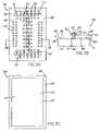
- FIG. 1Ais a top plan view of an embodiment of an integrated circuit die having bond pads in an I-shaped layout for fabricating an encapsulated board on chip (BOC) die unit according to an embodiment of a method of the invention.
- FIG. 1Bis a side elevational view of the integrated circuit die of FIG. 1A taken along line 1 B— 1 B.
- FIG. 2Ais top plan view of an embodiment of a support substrate having an I-shaped opening for use with the integrated circuit die of FIG. 1A .
- FIG. 2Bis a side elevational view of the support substrate of FIG. 2A taken along line 2 B— 2 B, showing an adhesive layer attached to the underside of the substrate.
- FIG. 3Ais a top plan view of a partially assembled die unit formed by mounting the integrated circuit die of FIG. 1A onto the underside of the support substrate of FIG. 2A .
- FIG. 3Bis a side elevational view of the die unit of FIG. 3A , taken along line 3 B— 3 B.
- FIG. 3Cis a bottom plan view of the die unit of FIG. 3A .
- FIG. 4is a top plan view of an embodiment of an adhesive layer for mounting the integrated circuit die of FIG. 1A onto the support substrate of FIG. 2A , the adhesive layer having an I-shaped opening.
- FIG. 5is a bottom plan view of the support substrate of FIG. 2A with another embodiment of an adhesive layer in the form of adhesive strips for mounting the die of FIG. 1A onto the underside of the support substrate.
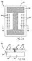
- FIG. 6Ais a top plan view of the die unit of FIG. 3A encapsulated (top molded) according to a method of the invention to form a package.
- FIG. 6Bis a side elevational view of the encapsulated package of FIG. 6A , taken along line 6 B— 6 B.
- FIG. 7Ais a top plan view of the encapsulated package of FIG. 6A , showing solder balls mounted thereon.
- FIG. 7Bis a side elevational view of the encapsulated package of FIG. 7A , taken along line 7 B— 7 B.
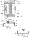
- FIG. 8Ais a top plan view of another embodiment of a die unit having a gap along the edge of the integrated circuit die and the wire bond slot of the support substrate.
- FIG. 8Bis a side elevational view of the die unit of FIG. 8A , taken along line 8 B— 8 B.
- FIG. 8Cis a bottom plan view of the die unit of FIG. 8A .
- FIG. 9Ais a top plan view of the die unit of FIG. 8A encapsulated (top molded) according to a method of the invention to form a die package.
- FIG. 9Bis a side elevational view of an embodiment of the encapsulated package of FIG. 9A taken along line 9 B,B′— 9 B,B′, and showing the die being fully overmolded.
- FIG. 9 B′is a side elevational view of another embodiment of the encapsulated die package of FIG. 9A , also taken along line 9 B,B′— 9 B,B′, and showing the sides of the die being overmolded and the second surface of the die exposed.
- FIG. 9Cis a bottom plan view of the encapsulated package shown in FIGS. 9A–9B .
- FIG. 9Dis a bottom plan view of the encapsulated package depicted in FIGS. 9 A– 9 B′.
- FIG. 10Ais a top plan view of the encapsulated die package of FIG. 9A showing solder balls mounted thereon.
- FIG. 10Bis a side elevational view of the die package of FIG. 10A , taken along line 10 B— 10 B.
- FIG. 11Ais a top plan view of another embodiment of a die unit having a gap along the edge of the integrated circuit die and the wire bond slot of the support substrate, and openings through the support substrate.
- FIGS. 11Bis a side elevational view of the die unit of FIG. 11A , taken along line 11 B— 11 B.
- FIG. 11Cis a bottom plan view of the die unit of FIG. 11A .
- FIG. 12Ais a top plan view of the die unit of FIG. 11A encapsulated according to a method of the invention.
- FIG. 12Bis a side elevational view of an embodiment of the encapsulated die package of FIG. 12A , taken along line 12 B,B′— 12 B,B′, and showing encapsulated sides and an exposed second surface of the die.
- FIG. 12 B′is a side elevational view of another embodiment of the encapsulated package of FIG. 12A , also taken along line 12 B,B′— 12 B, B′, showing the sides and second surface of the die being overmolded.
- FIG. 13Ais a top plan view of the encapsulated die package of FIG. 12A showing solder balls mounted thereon.
- FIGS. 13B , 13 B′are side elevational views of the encapsulated package of FIG. 13A , taken along line 13 B,B′— 13 B,B′, and corresponding to FIGS. 12B , 12 B′, respectively.
- FIGS. 14A–Eare sequential processing steps of an embodiment of a method of the invention for top gate molding the die unit shown in FIGS. 8A–8C .
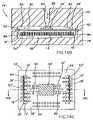
- FIG. 14Ais a top plan view of a panel or strip of mold units for fabricating multiple die packages, each mold unit having a top mold gate.
- FIG. 14Bis a side elevational view of a mold unit of FIG. 14A taken along line 14 B— 14 B, showing a die unit within a mold having a top mold gate oriented for downward delivery of a molding compound onto the die unit and flow of the molding compound around the die.
- FIG. 14Cis a top plan view of the die unit of FIG. 14B with the upper molding plate removed, showing direction of flow of the molding compound.
- FIG. 14Dis view of the resulting encapsulated die package within the mold.
- FIG. 14Eis a top plan view of the encapsulated die package.
- FIG. 15Ais a top plan view of another embodiment of a die unit having an elongate opening (wire bond slot).
- FIGS. 15B–15Care sequential processing steps for encapsulating the die unit of FIG. 15A according to an embodiment of a method of the invention utilizing the mold depicted in FIG. 14A .
- FIGS. 16A–Bare sequential processing steps of another embodiment of a method of the invention for top gate molding a die unit according to the invention.
- FIG. 16Ais a side elevational view of the die unit within another embodiment of a mold having a top mold gate oriented for downward delivery of a molding compound onto the die unit and positioned at an end of a molding plate, showing flow of the molding compound around the die.
- FIG. 16Bis a top plan view of the die unit of FIGS. 8A–8C within the mold of FIG. 16A , with the upper molding plate removed, showing direction of flow of the molding compound.
- FIG. 16 B′is a top plan view of the die unit of FIG. 15A within the mold of FIG. 16A , with the upper molding plate removed and showing direction of flow of the molding compound.
- FIG. 17Ais a side elevational view of another embodiment of a mold having a mold gate positioned for upward delivery of the molding compound onto the die unit, and the direction of flow of the compound.
- FIG. 17Bdepicts the encapsulated die package.
- top and bottomare used for illustrative purposes only, and are not meant to limit the description of the invention in any way.
- FIGS. 1–7An embodiment of an encapsulated integrated circuit die package and method of fabricating the package according to the invention is described with reference to FIGS. 1–7 , illustrating one-side encapsulation of the die.
- an integrated circuit (semiconductor) die 10is provided having a first (active) surface 12 , a second (inactive) surface 14 , and sides 16 , 18 .
- the first (active) surface 12 of the die 10has electrical elements (circuitry) and a plurality of bond pads 20 formed thereon.
- the bond pads 20are formed on the die 10 in an I-shaped layout.
- the first (active) surface 12 of the dieis mounted onto a support substrate 24 such that the bond pads 20 are exposed through an opening (wire bond slot) 30 in the support substrate.
- a support substrate 24is provided having a first (upper) side 26 , a second (under) side 28 , and a wire bond slot or opening 30 that corresponds to the bond pad layout on the die 10 .
- the support substrate 24typically comprises an electrically insulating material such as an organic polymer resin reinforced with glass fibers.
- An exemplary BGA support substratecomprises a reinforced polymer laminate material such as bismaleimide triazine (BT) resins, or a polyimide resin.
- a typical thickness of the support substrateis about 0.2 mm to about 1.6 mm.
- the support substrate 24includes an I-shaped wire bond slot or opening 30 that corresponds to the bond pad layout on the die 10 , through which wire bonding connects the bond pads 20 with contacts 32 on the upper side 26 of the support substrate 24 .
- the I-shaped wire bond slot 30has a main elongate segment 34 and a pair of shorter elongate segments 36 that are perpendicular to and on opposing ends 38 of the main elongate segment 34 .
- a plurality or series of bond pad fingers (contacts) 32are formed on the first (upper) side 26 of the support substrate 24 adjacent to the edge or periphery 40 of the wire bond slot 30 .
- the bond pad fingers 32comprise a conductive metal such as copper, aluminum, among others.
- a plurality of ball pads 42comprising a conductive metal layer and shown in a series of two parallel rows, are formed on the first (upper) side 26 of the support substrate 24 adjacent to the bond pad fingers 32 .
- the bond pad fingersare electrically connected to the ball pads 42 by traces (not shown) within the support substrate 24 .
- the first (active) surface 12 of the die 10is mounted against the underside 28 of the support substrate 24 , with the bond pads 20 exposed through the wire bond slot 30 in the support substrate 24 .
- Any conventional affixation techniquecan be used.
- the die 10can be secured to the support substrate 24 with an adhesive such as epoxy, an adhesive tape, or other available technique.
- a layer of adhesive tape 44is interposed between the support substrate 24 and the die 10 .
- the adhesive layer 44can comprise an adhesive sheet 46 having an I-shaped opening 48 that corresponds to the I-shaped wire bond slot 30 of the support substrate 24 , and can be attached to the underside 28 of the support structure 24 .
- the adhesive layer 44can comprise a pair of adhesive strips 50 that are positioned along opposite sides and adjacent to the I-shaped wire bond slot 30 on the underside 28 of the support substrate 24 . The adhesive layer 44 is applied to the underside 28 of the support structure along the edge of the opening 30 .
- bond wires 52are connected from the bond pads 20 on the die 10 through the wire bond slot 30 to the bond pad fingers 32 on the first (upper) side 26 of the support substrate 24 , resulting in a die-mounted and wire-bonded unit (“die unit”) 54 .
- the configuration of the illustrated die unit 54is known as a board-on-chip (BOC), in which the integrated circuit die or chip 10 is attached to the second (under) side 28 of a support substrate 24 .
- BOCboard-on-chip
- the BOC die unit 54can be encapsulated with a molding compound 56 to pot the bond wires 52 and the bond pad fingers 32 , and fill the wire bond slot 30 of the support substrate 24 to encapsulate the electronic components and the bond pads ( 20 ) on the first (active) surface 12 of the die 10 , resulting in an encapsulated package 58 .
- the second (inactive) surface 14 of the dieis exposed.
- the molding compound 56is dried, set or cured to a solid phase.
- the molding compoundis preferably a thermoset epoxy resin, for example, a novolac epoxy resin-based compound, that produces a rigid plastic body surrounding the die.
- solder balls 60can be conventionally bonded to the ball pads 42 , as depicted in FIGS. 7A–7B .
- a solder reflow processcan be used to bond the solder balls to the ball bond pads.
- the solder ballsprovide external electrical connections to the die, and permit the package to be surface mounted to a printed circuit board (PCB) or other electronic component.
- PCBprinted circuit board
- a heat sinkfor example, an extruded aluminum plate, a solder dam or ring, and other known devices (not shown), can be attached onto the die 10 to absorb and dissipate heat generated by electronic components.
- Heat sinksare known and used in the art, as described, for example, in U.S. Pat. No. 6,122,171 (Akram et al.).
- the molding compound 54is disposed partially upon the support substrate 24 and partially upon the first (active) surface 12 of the die 10 , with the second (inactive) surface 14 and sides 16 , 18 of the die 10 exposed and not covered by the molding compound.
- FIGS. 8–10Another embodiment of an encapsulated die package 58 ′ and method of the invention is illustrated in FIGS. 8–10 .
- the die unit 54 ′is structured to allow the molding compound to flow onto the sides, and, if desirable, the second (inactive) surface of the die to encapsulate the sides and the second surface of the die.
- the support substrate 24 ′is dimensioned such that mounting the first (active) surface 12 ′ of the die onto the underside 28 ′ of the support substrate 24 ′ provides a gap 62 ′ between a peripheral edge 64 ′ along side 16 ′ of the die 10 ′ and the wire bond slot 30 ′ of the support substrate 24 ′.
- the gaps 62 ′are formed along opposing edges 64 ′ along sides 16 ′ of the die 10 and outer edges 66 ′ of the shorter elongate segments 36 ′ of the wire bond slot 30 ′.
- the bond pads 20 ′ on the die 10 ′are then wire bonded to the bond pad fingers 32 ′ on the support substrate 24 ′, resulting in the die unit 54 ′.
- the die unit 54 ′can be encapsulated with a molding compound 56 ′ to cover the bond wires 52 ′, bond pad fingers 32 ′, and wire bond slot 30 ′ including electronic components and the bond pads 20 ′ on the first (active) surface 12 ′ of the die 10 ′.
- the molding compound 56 ′is flowed through the gap 62 ′ and onto the sides 16 ′, 18 ′, of the die 10 ′.
- the mold(not shown) into which the die unit 54 ′ is placed for the encapsulation step, is structured and sized to provide sufficient clearance (i.e., an open space) along the sides 16 ′, 18 ′ of the die 10 ′ into which the molding compound 56 ′ can flow to encapsulate the sides.
- the moldis structured to provide sufficient clearance along the second (inactive) surface 14 ′ of the die to allow the molding compound 56 ′ to flow over and encapsulate the second surface of the die, resulting in the die package 58 ′ shown in FIGS. 9B–9C .
- the moldcan also be structured to prevent the molding compound 56 ′ from flowing further onto the second (inactive) surface 14 ′ of the die 10 ′, such that the second (inactive) side of the die is exposed and not covered by the molding compound, resulting in the die package 58 ( 1 )′ as depicted in FIGS. 9 B′, 9 D.
- This embodiment 58 ( 1 )′ of the die packageprovides a package having a reduced height (thickness), resulting in a thinner package overall.
- solder balls 60 ′can be bonded to the ball pads 42 ′ on the first (upper) surface 26 ′ of the support structure 24 ′, as depicted in FIGS. 10A–10B .
- FIGS. 11–13Yet another embodiment of a die package 58 ′′ and method according to invention is illustrated in FIGS. 11–13 .
- the die unit 54 ′′is again structured to allow the molding compound to flow onto and encapsulate the sides and, optionally, the second (inactive) surface of the die.
- the support substrate 24 ′′is provided with holes 68 ′′ therethrough, which are positioned adjacent to the opposing ends 70 ′′ of the shorter elongate segments 36 ′′ of the I-shaped wire bond slot 30 ′′.
- the die 10 ′′ and the support substrate 24 ′are dimensioned and configured such that mounting the first (active) surface 12 ′′ of the die 10 ′′ onto the underside 28 ′′ of the support substrate 24 ′′ forms a gap 72 ′′ between a peripheral edge 74 ′′ along the side 18 ′′ of the die 10 ′′ and the opposing ends 70 ′′ of the shorter elongate segments 36 ′′ of the wire bond slot 30 ′′, and also leaves the holes 68 ′′ through the support substrate 24 uncovered.
- the bond pads 20 ′′ on the die 10 ′′are then wire bonded to the bond pad fingers 32 ′′ on the support substrate 24 ′′, resulting in the die unit 54 ′′.
- the molding compound 56 ′′is flowed over the bonding wires 52 ′′ and bond pad fingers 32 ′′ and to fill the I-shaped wire bond slot 30 ′′, as depicted in FIG. 12A .
- the molding compound 56 ′′is further flowed through the gaps 72 ′′ and the holes 68 ′′ in the substrate 24 ′′ onto the sides 16 ′′, 18 ′′ of the die 10 ′′, as depicted in FIG. 12B , resulting in the die package 58 ′′.
- the molding compound 56 ′′can be flowed onto the second (inactive) surface 14 ′′ of the die 10 ′′ as depicted in FIG. 12 B′, resulting in the die package 58 ( 1 )′′.
- Solder balls 60 ′′can then be bonded to the ball pads 42 ′′ on the upper surface 26 ′′ of the support structure 24 ′′, as depicted in FIG. 13A and in cross-sectional view in FIGS. 13B , 13 B′, corresponding to the embodiments depicted in FIGS. 12B , 12 B′, respectively.
- the die unit 54 ′′can be structured with either or both of the described hole(s) 68 ′′ or gap(s) 72 ′′.
- the inventioncan be applied to encapsulate one or both surfaces (and sides) of an IC die.
- FIGS. 14A–14Ean embodiment of a mold 74 and method of encapsulating an integrated circuit die unit according to the invention will be described with reference to the die unit 54 ′ depicted in FIGS. 8A–8C , which includes gaps 62 ′ along the edges 64 ′ of the integrated circuit die 10 ′ and segment 36 ′ of the wire bond slot 30 ′.
- the mold 74can be initially a segment (A) of a panel or strip 75 to fabricate multiple die packages. Following the fabrication process for the packages, the panel 75 is singulated into individual BGA packages. As depicted in FIG.
- the mold 74includes first and second plate members (mold halves) 76 , 78 , that define a chamber 80 , the first plate member 76 having a top mold gate (pin cavity) 82 to provide a conduit for introducing a molding compound 56 ′ into the chamber 80 . It is understood that the described mold and method can be utilized for one-side encapsulation of an IC die as depicted with reference to FIGS. 1–7 .
- the mold 74is sized and structured to provide sufficient clearance (i.e., an open space 84 , 86 ) along the sides 16 ′, 18 ′ and, if desired, along the second (inactive) surface 14 ′ of the die 10 ′, into which the molding compound 56 ′ can flow to encapsulate the sides and second surface of the die. If it is desired that the second surface 14 ′ of the die 10 ′ remain exposed, the mold 74 can be structured to eliminate the open space 86 adjacent the second surface 14 ′ of the die 10 ′.
- the molding plateshave been modified from a conventional configuration such that the mold gate 82 is formed in one of the first or second plate members 76 , 78 , and is oriented perpendicular to the upper side 28 ′ of the support substrate 24 ′ and the first (active) surface 12 ′ of the die 10 ′ of the die unit 54 ′ positioned in the mold 74 .
- the molding compound 56 ′passes through the mold gate 82 in the direction of arrow 88 , and flows directly onto the upper side 28 ′ of the substrate and into the wire bond slot 30 ′.
- the molding compound 56is flowed through the mold gate 82 under pressure, typically at about 500 psi to about 2,000 psi.
- the mold gate 82is located in the first plate member 76 (and oriented perpendicular to the second plate member 78 ) to dispense the molding compound 56 ′ in a downward direction (arrow 88 ) onto the die unit 54 ′ at about the center of the main elongate segment 34 ′ of the I-shaped wire bond slot 30 ′ of the support substrate 24 ′.
- the molding compound 56 ′is then flowed over the support substrate 24 ′ and active surface 12 ′ of the die 10 ′ along the main elongate segment 34 ′ in the direction of the arrows 90 to the shorter elongate segments 36 ′ of the wire bond slot 30 ′.
- the molding compound 56 ′is then flowed through the gap 62 ′ (arrow 92 ) and into the open spaces 84 , 86 to cover the sides 16 ′, 18 ′ and the second surface 14 ′ of the die 10 ′.
- the resulting encapsulated package 58 ′is depicted in FIGS. 14D–14E .
- the method and mold described with reference to FIGS. 14A–14Ecan also be used to similarly encapsulate a die unit 54 ′′′ in which the wire bond slot in the support substrate is a different configuration such as an elongate opening 30 ′′′, as depicted in FIG. 15A .
- the die unit 54 ′′′can include a gap 62 ′′′ and/or hole 68 ′′′ for passage of the molding compound 56 ′′′ onto the sides 16 ′′′, 18 ′′′, and the second (inactive) surface 14 ′′′ of the die 10 ′′′.
- the mold 74described in connection with FIGS.
- the molding compound 56 ′′′can be flowed onto about the center 92 ′′′ of the elongate opening 30 ′′′ and to either end in the direction of arrows 90 ′′′, as shown in FIG. 15B .
- the molding compound 56 ′′′can then be flowed through the gap 62 ′′′ and/or hole 68 ′′′ onto the sides ( 16 ′′′, 18 ′′′) of the die, and optionally onto the second surface ( 14 ′′′) of the die 10 ′′′ as desired (see FIG. 14B ), resulting in the encapsulated package 58 ′′′ depicted in FIG. 15C (and in cross-section in FIG. 14D ).
- top (or bottom) mold gatepin cavity
- the mold gatecan be located in the first or second plate members to dispense the molding compound directly onto the upper surface of the support substrate and the first (active) surface of the die of the die unit at any point along the wire bond slot of the support substrate.
- FIGS. 16A–16BAnother embodiment of a mold 74 ′, is illustrated in FIGS. 16A–16B .
- the mold gate 82 ′is located at one end of the first plate member 76 ′ to dispense the molding compound 56 ′ in a downward direction at or near a first end 30 ′ of the main elongate segment 34 ′ of the I-shaped wire bond slot 30 ′ in the support substrate 24 ′.
- the molding compound 56 ′is introduced through the mold gate 82 ′ in the direction of arrow 88 ′ onto the substrate 24 ′ and into the wire bond slot 30 ′.
- the molding compound 56 ′is flowed in the direction of arrows 90 ′ to the shorter elongate segments 36 ′ of the wire bond slot 30 ′, and through the gap 62 ′ (and/or holes) in the direction of arrows 92 ′. As depicted, the molding compound 56 ′ is flowed onto the sides 16 ′ of the die 10 ′ and (optionally) the second surface 14 ′ of the die 10 ′, resulting in a die package 58 ′, such as depicted in FIGS. 14D–14E .
- the mold 74 , 74 ′can be used to encapsulate a die unit having a different shaped wire bond slot in the substrate and bond pad layout, for example, the die unit 54 ′′′ having an elongate slot (opening) 30 ′′′ and pad layout, as shown in FIG. 15A .
- the molding compound 56 ′′′can be flowed onto an end 38 a ′′′ of the elongate opening 30 ′′′ ( FIGS.
- the mold gate 82 , 82 ′is shown as being oriented with respect to the die unit to allow the molding compound to be introduced through the mold gate in a downwardly direction (arrow 88 , 88 ′) directly onto the first (active) surface of the die.
- the downward flow of the molding compoundcan apply an amount of pressure onto the die unit that causes the support substrate and die to bend.
- the mold gate 82 ′′is oriented with respect to the die unit 54 ′ such that the molding compound 56 ′′ is delivered through the mold gate 82 ′′ in an upward direction (arrows 96 ′′) onto the upper surface 28 ′ of the support substrate 24 ′ and into the wire bond slot ( 30 ′), and can be further flowed through a gap 62 ′ and/or hole 68 ′ in the direction of arrows 92 ′′ onto the sides 16 ′, 18 ′, and the second (inactive) surface 14 ′ of the die 10 ′, resulting in the encapsulated package 58 ′ shown in FIG. 17B .
- the advantage of orienting the die over the substrate during the molding process and flowing the molding compound 56 ′′ in an upward direction onto the die unitprovides an additional weight or force to present the substrate from bowing or bending.
- the mold gate 82 ′′can be located in the second plate member 78 ′ (as shown), or in the first plate member ( 76 ) as illustrated in FIG. 14D whereby the mold ( 74 ) can be flipped so that the molding compound can be flowed in a vertical direction (arrow 96 ′′) as depicted in FIG. 17A .
- Either a conventional (side) mold gate molding process or the present top gate molding processcan be utilized to encapsulate the BOC BGA die unit.
- Current molding methods of BOC devicesutilize a mold having a mold gate along a side (perimeter) of the lower plate and positioned adjacent to the die edge.
- the encapsulant materialis dispensed horizontally into a side of the mold and flows under and over the support substrate onto the active surface of the die to cover the wire bonds.
- the molding compoundenters the mold through a mold gate positioned in the surface of the first (or second) molding plate, perpendicular to the other molding plate and the surface of the die unit in the mold.
- the side-positioned mold gate in the lower molding plateis lined with a gold-plated copper foil to prevent encapsulant material from adhering to the edges of the substrate.
- the top mold gate of the present mold apparatusdoes not require a gold surface area on the substrate, thus providing a reduction in the substrate cost in the manufacture of BOC FBGA packages.
- the present top gate molding processalso optimizes mold yield (the number of acceptable molded packages), compared to conventional BOC molding processes, by reducing the number of rejected or substandard packages.
- the use of the present top gate molding processadvantageously eliminates the need for a diversion dam. Also, unlike current molding processes that require different diversion dam locations and heights to accommodate different tape thicknesses, the use of the present top gate molding process can be successfully applied to die units over a wide range of tape thicknesses. Elimination of the diversion dam also reduces package size configuration. In addition, the top gate molding process requires fewer process steps for substrate fabrication, resulting in shorter substrate delivery lead time and lower substrate costs.
Landscapes
- Engineering & Computer Science (AREA)
- Microelectronics & Electronic Packaging (AREA)
- Computer Hardware Design (AREA)
- Power Engineering (AREA)
- Physics & Mathematics (AREA)
- Condensed Matter Physics & Semiconductors (AREA)
- General Physics & Mathematics (AREA)
- Manufacturing & Machinery (AREA)
- Encapsulation Of And Coatings For Semiconductor Or Solid State Devices (AREA)
- Structures Or Materials For Encapsulating Or Coating Semiconductor Devices Or Solid State Devices (AREA)
Abstract
Description
Claims (33)
Priority Applications (1)
| Application Number | Priority Date | Filing Date | Title |
|---|---|---|---|
| US10/408,990US7112048B2 (en) | 2001-12-12 | 2003-04-08 | BOC BGA package for die with I-shaped bond pad layout |
Applications Claiming Priority (4)
| Application Number | Priority Date | Filing Date | Title |
|---|---|---|---|
| SG200107789ASG118103A1 (en) | 2001-12-12 | 2001-12-12 | BOC BGA package for die with I-shaped bond pad layout |
| SG200107789-0 | 2001-12-12 | ||
| US10/068,165US6692987B2 (en) | 2001-12-12 | 2002-02-05 | BOC BGA package for die with I-shaped bond pad layout |
| US10/408,990US7112048B2 (en) | 2001-12-12 | 2003-04-08 | BOC BGA package for die with I-shaped bond pad layout |
Related Parent Applications (1)
| Application Number | Title | Priority Date | Filing Date |
|---|---|---|---|
| US10/068,165DivisionUS6692987B2 (en) | 2001-12-12 | 2002-02-05 | BOC BGA package for die with I-shaped bond pad layout |
Publications (2)
| Publication Number | Publication Date |
|---|---|
| US20030211660A1 US20030211660A1 (en) | 2003-11-13 |
| US7112048B2true US7112048B2 (en) | 2006-09-26 |
Family
ID=36102687
Family Applications (2)
| Application Number | Title | Priority Date | Filing Date |
|---|---|---|---|
| US10/408,972Expired - LifetimeUS6720666B2 (en) | 2001-12-12 | 2003-04-08 | BOC BGA package for die with I-shaped bond pad layout |
| US10/408,990Expired - LifetimeUS7112048B2 (en) | 2001-12-12 | 2003-04-08 | BOC BGA package for die with I-shaped bond pad layout |
Family Applications Before (1)
| Application Number | Title | Priority Date | Filing Date |
|---|---|---|---|
| US10/408,972Expired - LifetimeUS6720666B2 (en) | 2001-12-12 | 2003-04-08 | BOC BGA package for die with I-shaped bond pad layout |
Country Status (2)
| Country | Link |
|---|---|
| US (2) | US6720666B2 (en) |
| SG (1) | SG118103A1 (en) |
Cited By (2)
| Publication number | Priority date | Publication date | Assignee | Title |
|---|---|---|---|---|
| US20080185702A1 (en)* | 2007-02-07 | 2008-08-07 | Zigmund Ramirez Camacho | Multi-chip package system with multiple substrates |
| US20100155957A1 (en)* | 2007-06-07 | 2010-06-24 | Silicon Works Co., Ltd. | Pad layout structure of semiconductor chip |
Families Citing this family (48)
| Publication number | Priority date | Publication date | Assignee | Title |
|---|---|---|---|---|
| US6757262B1 (en)* | 2000-09-15 | 2004-06-29 | Motorola, Inc. | Service framework supporting remote service discovery and connection |
| US7102217B2 (en)* | 2003-04-09 | 2006-09-05 | Micron Technology, Inc. | Interposer substrates with reinforced interconnect slots, and semiconductor die packages including same |
| JP4222920B2 (en)* | 2003-10-01 | 2009-02-12 | 株式会社ルネサステクノロジ | Semiconductor device |
| JP2006339317A (en)* | 2005-05-31 | 2006-12-14 | Toshiba Corp | Surface mount semiconductor device |
| US20070145506A1 (en)* | 2005-12-28 | 2007-06-28 | Feng Chen | Assembly of image-sensing chip and circuit board with inward wire bonding |
| US20070241441A1 (en)* | 2006-04-17 | 2007-10-18 | Stats Chippac Ltd. | Multichip package system |
| US20080088030A1 (en)* | 2006-10-16 | 2008-04-17 | Formfactor, Inc. | Attaching and interconnecting dies to a substrate |
| KR100766502B1 (en)* | 2006-11-09 | 2007-10-15 | 삼성전자주식회사 | Semiconductor device package |
| CN101207972B (en)* | 2006-12-22 | 2010-05-19 | 鸿富锦精密工业(深圳)有限公司 | A circuit board and photosensitive device using the same |
| JP2009182104A (en)* | 2008-01-30 | 2009-08-13 | Toshiba Corp | Semiconductor package |
| JP5550369B2 (en)* | 2010-02-03 | 2014-07-16 | 新日鉄住金マテリアルズ株式会社 | Copper bonding wire for semiconductor and its bonding structure |
| US8553420B2 (en) | 2010-10-19 | 2013-10-08 | Tessera, Inc. | Enhanced stacked microelectronic assemblies with central contacts and improved thermal characteristics |
| US8304881B1 (en) | 2011-04-21 | 2012-11-06 | Tessera, Inc. | Flip-chip, face-up and face-down wirebond combination package |
| US8633576B2 (en) | 2011-04-21 | 2014-01-21 | Tessera, Inc. | Stacked chip-on-board module with edge connector |
| US9013033B2 (en) | 2011-04-21 | 2015-04-21 | Tessera, Inc. | Multiple die face-down stacking for two or more die |
| US8952516B2 (en) | 2011-04-21 | 2015-02-10 | Tessera, Inc. | Multiple die stacking for two or more die |
| US8338963B2 (en) | 2011-04-21 | 2012-12-25 | Tessera, Inc. | Multiple die face-down stacking for two or more die |
| US8970028B2 (en) | 2011-12-29 | 2015-03-03 | Invensas Corporation | Embedded heat spreader for package with multiple microelectronic elements and face-down connection |
| US8928153B2 (en) | 2011-04-21 | 2015-01-06 | Tessera, Inc. | Flip-chip, face-up and face-down centerbond memory wirebond assemblies |
| US8823165B2 (en) | 2011-07-12 | 2014-09-02 | Invensas Corporation | Memory module in a package |
| US8513817B2 (en) | 2011-07-12 | 2013-08-20 | Invensas Corporation | Memory module in a package |
| US8502390B2 (en) | 2011-07-12 | 2013-08-06 | Tessera, Inc. | De-skewed multi-die packages |
| US8441111B2 (en) | 2011-10-03 | 2013-05-14 | Invensas Corporation | Stub minimization for multi-die wirebond assemblies with parallel windows |
| US8436457B2 (en) | 2011-10-03 | 2013-05-07 | Invensas Corporation | Stub minimization for multi-die wirebond assemblies with parallel windows |
| US8405207B1 (en) | 2011-10-03 | 2013-03-26 | Invensas Corporation | Stub minimization for wirebond assemblies without windows |
| KR101894823B1 (en) | 2011-10-03 | 2018-09-04 | 인벤사스 코포레이션 | Stub minimization for multi-die wirebond assemblies with parallel windows |
| TWI515864B (en) | 2011-10-03 | 2016-01-01 | 英帆薩斯公司 | Stub minimization with terminal grids offset from center of package |
| JP5947904B2 (en) | 2011-10-03 | 2016-07-06 | インヴェンサス・コーポレイション | Stub minimization for multi-die wirebond assemblies with orthogonal windows |
| WO2013052345A1 (en)* | 2011-10-03 | 2013-04-11 | Invensas Corporation | Stub minimization for assemblies without wirebonds to package substrate |
| US8525327B2 (en) | 2011-10-03 | 2013-09-03 | Invensas Corporation | Stub minimization for assemblies without wirebonds to package substrate |
| US8436477B2 (en) | 2011-10-03 | 2013-05-07 | Invensas Corporation | Stub minimization using duplicate sets of signal terminals in assemblies without wirebonds to package substrate |
| US8653646B2 (en) | 2011-10-03 | 2014-02-18 | Invensas Corporation | Stub minimization using duplicate sets of terminals for wirebond assemblies without windows |
| US8345441B1 (en) | 2011-10-03 | 2013-01-01 | Invensas Corporation | Stub minimization for multi-die wirebond assemblies with parallel windows |
| US8848391B2 (en) | 2012-08-27 | 2014-09-30 | Invensas Corporation | Co-support component and microelectronic assembly |
| US9368477B2 (en) | 2012-08-27 | 2016-06-14 | Invensas Corporation | Co-support circuit panel and microelectronic packages |
| US8787034B2 (en) | 2012-08-27 | 2014-07-22 | Invensas Corporation | Co-support system and microelectronic assembly |
| US8848392B2 (en) | 2012-08-27 | 2014-09-30 | Invensas Corporation | Co-support module and microelectronic assembly |
| TWI581396B (en)* | 2012-10-17 | 2017-05-01 | 環旭電子股份有限公司 | Three-dimensional stacked package structure and manufacturing method thereof |
| US9070423B2 (en) | 2013-06-11 | 2015-06-30 | Invensas Corporation | Single package dual channel memory with co-support |
| US9123555B2 (en) | 2013-10-25 | 2015-09-01 | Invensas Corporation | Co-support for XFD packaging |
| US9281296B2 (en) | 2014-07-31 | 2016-03-08 | Invensas Corporation | Die stacking techniques in BGA memory package for small footprint CPU and memory motherboard design |
| US9691437B2 (en) | 2014-09-25 | 2017-06-27 | Invensas Corporation | Compact microelectronic assembly having reduced spacing between controller and memory packages |
| US9484080B1 (en) | 2015-11-09 | 2016-11-01 | Invensas Corporation | High-bandwidth memory application with controlled impedance loading |
| US9679613B1 (en) | 2016-05-06 | 2017-06-13 | Invensas Corporation | TFD I/O partition for high-speed, high-density applications |
| WO2019005152A1 (en)* | 2017-06-30 | 2019-01-03 | Intel Corporation | Die back side structures for warpage control |
| TWI667746B (en)* | 2018-04-03 | 2019-08-01 | 南茂科技股份有限公司 | Semiconductor package structure and method for manufacturing the same |
| CN113284856B (en)* | 2020-02-19 | 2022-03-18 | 长鑫存储技术有限公司 | Package structure and method for forming the same |
| US11296034B2 (en)* | 2020-06-18 | 2022-04-05 | Advanced Semiconductor Engineering, Inc. | Substrate and semiconductor package comprising an interposer element with a slot and method of manufacturing the same |
Citations (33)
| Publication number | Priority date | Publication date | Assignee | Title |
|---|---|---|---|---|
| US4250347A (en)* | 1977-05-05 | 1981-02-10 | Fierkens Richardus H | Method of encapsulating microelectronic elements |
| US4812114A (en)* | 1987-09-30 | 1989-03-14 | Texas Instruments Incorporated | New IC molding process |
| US4915607A (en)* | 1987-09-30 | 1990-04-10 | Texas Instruments Incorporated | Lead frame assembly for an integrated circuit molding system |
| US5134773A (en)* | 1989-05-26 | 1992-08-04 | Gerard Lemaire | Method for making a credit card containing a microprocessor chip |
| US5218759A (en)* | 1991-03-18 | 1993-06-15 | Motorola, Inc. | Method of making a transfer molded semiconductor device |
| US5254501A (en) | 1992-09-11 | 1993-10-19 | Cypress Semiconductor Corporation | Same-side gated process for encapsulating semiconductor devices |
| US5302850A (en)* | 1989-09-18 | 1994-04-12 | Seiko Epson Corporation | Semiconductor sealing mold |
| US5385869A (en)* | 1993-07-22 | 1995-01-31 | Motorola, Inc. | Semiconductor chip bonded to a substrate and method of making |
| US5461255A (en) | 1992-09-18 | 1995-10-24 | Texas Instruments Incorporated | Multi-layered lead frame assembly for integrated circuits |
| US5563103A (en)* | 1992-02-10 | 1996-10-08 | Nec Corporation | Method for manufacturing thermoplastic resin molded semiconductor |
| US5570272A (en)* | 1993-08-18 | 1996-10-29 | Lsi Logic Corporation | Apparatus for encapsulating an integrated circuit package |
| US6001672A (en)* | 1997-02-25 | 1999-12-14 | Micron Technology, Inc. | Method for transfer molding encapsulation of a semiconductor die with attached heat sink |
| US6048755A (en) | 1998-11-12 | 2000-04-11 | Micron Technology, Inc. | Method for fabricating BGA package using substrate with patterned solder mask open in die attach area |
| US6081997A (en)* | 1997-08-14 | 2000-07-04 | Lsi Logic Corporation | System and method for packaging an integrated circuit using encapsulant injection |
| US6122171A (en) | 1999-07-30 | 2000-09-19 | Micron Technology, Inc. | Heat sink chip package and method of making |
| US6173490B1 (en) | 1997-08-20 | 2001-01-16 | National Semiconductor Corporation | Method for forming a panel of packaged integrated circuits |
| US6177723B1 (en) | 1997-04-10 | 2001-01-23 | Texas Instruments Incorporated | Integrated circuit package and flat plate molding process for integrated circuit package |
| US6184465B1 (en) | 1998-11-12 | 2001-02-06 | Micron Technology, Inc. | Semiconductor package |
| US6210992B1 (en) | 1999-08-31 | 2001-04-03 | Micron Technology, Inc. | Controlling packaging encapsulant leakage |
| US6229204B1 (en) | 1998-09-03 | 2001-05-08 | Micron Technology, Inc. | Chip on board with heat sink attachment |
| US6268650B1 (en) | 1999-05-25 | 2001-07-31 | Micron Technology, Inc. | Semiconductor device, ball grid array connection system, and method of making |
| US6284569B1 (en) | 1998-02-05 | 2001-09-04 | Asat, Limited | Method of manufacturing a flexible integrated circuit package utilizing an integrated carrier ring/stiffener |
| US6287503B1 (en) | 1998-02-05 | 2001-09-11 | Micron Technology, Inc. | Method for encasing array packages |
| US6294825B1 (en) | 1999-02-22 | 2001-09-25 | Micron Technology, Inc. | Asymmetrical mold of multiple-part matrixes |
| US20020072153A1 (en) | 2000-05-08 | 2002-06-13 | Lee Kian Chai | Method and apparatus for distributing mold material in a mold for packaging microelectronic devices |
| US6413801B1 (en)* | 2000-05-02 | 2002-07-02 | Advanced Semiconductor Engineering, Inc. | Method of molding semiconductor device and molding die for use therein |
| US6439869B1 (en) | 2000-08-16 | 2002-08-27 | Micron Technology, Inc. | Apparatus for molding semiconductor components |
| US6469399B2 (en) | 1999-02-08 | 2002-10-22 | Advanced Semiconductor Engineering, Inc. | Semiconductor package |
| US6473311B1 (en)* | 2000-06-02 | 2002-10-29 | Micro Technology, Inc. | Gate area relief strip for a molded I/C package |
| US20020172024A1 (en) | 2001-05-21 | 2002-11-21 | Hui Chong Chin | Method for encapsulating intermediate conductive elements connecting a semiconductor die to a substrate and semiconductor devices so packaged |
| US6486536B1 (en)* | 2000-08-29 | 2002-11-26 | Micron Technology, Inc. | U-shape tape for BOC FBGA package to improve moldability |
| US6525421B1 (en)* | 2001-05-01 | 2003-02-25 | Lsi Logic Corporation | Molded integrated circuit package |
| US20030042617A1 (en) | 2001-08-21 | 2003-03-06 | Lee Teck Kheng | Microelectronic devices and methods of manufacture |
Family Cites Families (2)
| Publication number | Priority date | Publication date | Assignee | Title |
|---|---|---|---|---|
| US72153A (en)* | 1867-12-17 | Abeam alexander | ||
| US6290839B1 (en)* | 1998-06-23 | 2001-09-18 | Clinical Micro Sensors, Inc. | Systems for electrophoretic transport and detection of analytes |
- 2001
- 2001-12-12SGSG200107789Apatent/SG118103A1/enunknown
- 2003
- 2003-04-08USUS10/408,972patent/US6720666B2/ennot_activeExpired - Lifetime
- 2003-04-08USUS10/408,990patent/US7112048B2/ennot_activeExpired - Lifetime
Patent Citations (33)
| Publication number | Priority date | Publication date | Assignee | Title |
|---|---|---|---|---|
| US4250347A (en)* | 1977-05-05 | 1981-02-10 | Fierkens Richardus H | Method of encapsulating microelectronic elements |
| US4812114A (en)* | 1987-09-30 | 1989-03-14 | Texas Instruments Incorporated | New IC molding process |
| US4915607A (en)* | 1987-09-30 | 1990-04-10 | Texas Instruments Incorporated | Lead frame assembly for an integrated circuit molding system |
| US5134773A (en)* | 1989-05-26 | 1992-08-04 | Gerard Lemaire | Method for making a credit card containing a microprocessor chip |
| US5302850A (en)* | 1989-09-18 | 1994-04-12 | Seiko Epson Corporation | Semiconductor sealing mold |
| US5218759A (en)* | 1991-03-18 | 1993-06-15 | Motorola, Inc. | Method of making a transfer molded semiconductor device |
| US5563103A (en)* | 1992-02-10 | 1996-10-08 | Nec Corporation | Method for manufacturing thermoplastic resin molded semiconductor |
| US5254501A (en) | 1992-09-11 | 1993-10-19 | Cypress Semiconductor Corporation | Same-side gated process for encapsulating semiconductor devices |
| US5461255A (en) | 1992-09-18 | 1995-10-24 | Texas Instruments Incorporated | Multi-layered lead frame assembly for integrated circuits |
| US5385869A (en)* | 1993-07-22 | 1995-01-31 | Motorola, Inc. | Semiconductor chip bonded to a substrate and method of making |
| US5570272A (en)* | 1993-08-18 | 1996-10-29 | Lsi Logic Corporation | Apparatus for encapsulating an integrated circuit package |
| US6001672A (en)* | 1997-02-25 | 1999-12-14 | Micron Technology, Inc. | Method for transfer molding encapsulation of a semiconductor die with attached heat sink |
| US6177723B1 (en) | 1997-04-10 | 2001-01-23 | Texas Instruments Incorporated | Integrated circuit package and flat plate molding process for integrated circuit package |
| US6081997A (en)* | 1997-08-14 | 2000-07-04 | Lsi Logic Corporation | System and method for packaging an integrated circuit using encapsulant injection |
| US6173490B1 (en) | 1997-08-20 | 2001-01-16 | National Semiconductor Corporation | Method for forming a panel of packaged integrated circuits |
| US6284569B1 (en) | 1998-02-05 | 2001-09-04 | Asat, Limited | Method of manufacturing a flexible integrated circuit package utilizing an integrated carrier ring/stiffener |
| US6287503B1 (en) | 1998-02-05 | 2001-09-11 | Micron Technology, Inc. | Method for encasing array packages |
| US6229204B1 (en) | 1998-09-03 | 2001-05-08 | Micron Technology, Inc. | Chip on board with heat sink attachment |
| US6048755A (en) | 1998-11-12 | 2000-04-11 | Micron Technology, Inc. | Method for fabricating BGA package using substrate with patterned solder mask open in die attach area |
| US6184465B1 (en) | 1998-11-12 | 2001-02-06 | Micron Technology, Inc. | Semiconductor package |
| US6469399B2 (en) | 1999-02-08 | 2002-10-22 | Advanced Semiconductor Engineering, Inc. | Semiconductor package |
| US6294825B1 (en) | 1999-02-22 | 2001-09-25 | Micron Technology, Inc. | Asymmetrical mold of multiple-part matrixes |
| US6268650B1 (en) | 1999-05-25 | 2001-07-31 | Micron Technology, Inc. | Semiconductor device, ball grid array connection system, and method of making |
| US6122171A (en) | 1999-07-30 | 2000-09-19 | Micron Technology, Inc. | Heat sink chip package and method of making |
| US6210992B1 (en) | 1999-08-31 | 2001-04-03 | Micron Technology, Inc. | Controlling packaging encapsulant leakage |
| US6413801B1 (en)* | 2000-05-02 | 2002-07-02 | Advanced Semiconductor Engineering, Inc. | Method of molding semiconductor device and molding die for use therein |
| US20020072153A1 (en) | 2000-05-08 | 2002-06-13 | Lee Kian Chai | Method and apparatus for distributing mold material in a mold for packaging microelectronic devices |
| US6473311B1 (en)* | 2000-06-02 | 2002-10-29 | Micro Technology, Inc. | Gate area relief strip for a molded I/C package |
| US6439869B1 (en) | 2000-08-16 | 2002-08-27 | Micron Technology, Inc. | Apparatus for molding semiconductor components |
| US6486536B1 (en)* | 2000-08-29 | 2002-11-26 | Micron Technology, Inc. | U-shape tape for BOC FBGA package to improve moldability |
| US6525421B1 (en)* | 2001-05-01 | 2003-02-25 | Lsi Logic Corporation | Molded integrated circuit package |
| US20020172024A1 (en) | 2001-05-21 | 2002-11-21 | Hui Chong Chin | Method for encapsulating intermediate conductive elements connecting a semiconductor die to a substrate and semiconductor devices so packaged |
| US20030042617A1 (en) | 2001-08-21 | 2003-03-06 | Lee Teck Kheng | Microelectronic devices and methods of manufacture |
Cited By (4)
| Publication number | Priority date | Publication date | Assignee | Title |
|---|---|---|---|---|
| US20080185702A1 (en)* | 2007-02-07 | 2008-08-07 | Zigmund Ramirez Camacho | Multi-chip package system with multiple substrates |
| US7750451B2 (en) | 2007-02-07 | 2010-07-06 | Stats Chippac Ltd. | Multi-chip package system with multiple substrates |
| US20100155957A1 (en)* | 2007-06-07 | 2010-06-24 | Silicon Works Co., Ltd. | Pad layout structure of semiconductor chip |
| US8258631B2 (en)* | 2007-06-07 | 2012-09-04 | Silicon Works Co., Ltd. | Pad layout structure of semiconductor chip |
Also Published As
| Publication number | Publication date |
|---|---|
| US6720666B2 (en) | 2004-04-13 |
| US20030211660A1 (en) | 2003-11-13 |
| SG118103A1 (en) | 2006-01-27 |
| US20030211659A1 (en) | 2003-11-13 |
Similar Documents
| Publication | Publication Date | Title |
|---|---|---|
| US7112048B2 (en) | BOC BGA package for die with I-shaped bond pad layout | |
| US6692987B2 (en) | BOC BGA package for die with I-shaped bond pad layout | |
| US7501309B2 (en) | Standoffs for centralizing internals in packaging process | |
| US7618849B2 (en) | Integrated circuit package with etched leadframe for package-on-package interconnects | |
| US6767767B2 (en) | Method of manufacturing a semiconductor device in which a block molding package utilizes air vents in a substrate | |
| US5557150A (en) | Overmolded semiconductor package | |
| US6534859B1 (en) | Semiconductor package having heat sink attached to pre-molded cavities and method for creating the package | |
| US5474958A (en) | Method for making semiconductor device having no die supporting surface | |
| US7170158B2 (en) | Double-sided circuit board and multi-chip package including such a circuit board and method for manufacture | |
| US7598599B2 (en) | Semiconductor package system with substrate having different bondable heights at lead finger tips | |
| US20020185751A1 (en) | Semiconductor chip package having a semiconductor chip with center and edge bonding pads and manufacturing method thereof | |
| US7692276B2 (en) | Thermally enhanced ball grid array package formed in strip with one-piece die-attached exposed heat spreader | |
| US20160013075A1 (en) | Integrated circuit package and process for fabricating the same | |
| US6245598B1 (en) | Method for wire bonding a chip to a substrate with recessed bond pads and devices formed | |
| US6677665B2 (en) | Dual-die integrated circuit package | |
| US7049173B2 (en) | Method for fabricating semiconductor component with chip on board leadframe | |
| US6558981B2 (en) | Method for making an encapsulated semiconductor chip module | |
| JP3482888B2 (en) | Resin-sealed semiconductor device and method of manufacturing the same | |
| US6650005B2 (en) | Micro BGA package | |
| US20050062152A1 (en) | Window ball grid array semiconductor package with substrate having opening and mehtod for fabricating the same | |
| KR100487135B1 (en) | Ball Grid Array Package | |
| US6875639B2 (en) | Semiconductor device and method of manufacturing the same | |
| US6717278B2 (en) | Semiconductor device having a resist edge positioned over througholes | |
| KR100195507B1 (en) | Slim type semiconductor chip package device |
Legal Events
| Date | Code | Title | Description |
|---|---|---|---|
| FEPP | Fee payment procedure | Free format text:PAYOR NUMBER ASSIGNED (ORIGINAL EVENT CODE: ASPN); ENTITY STATUS OF PATENT OWNER: LARGE ENTITY | |
| STCF | Information on status: patent grant | Free format text:PATENTED CASE | |
| FPAY | Fee payment | Year of fee payment:4 | |
| FPAY | Fee payment | Year of fee payment:8 | |
| AS | Assignment | Owner name:U.S. BANK NATIONAL ASSOCIATION, AS COLLATERAL AGENT, CALIFORNIA Free format text:SECURITY INTEREST;ASSIGNOR:MICRON TECHNOLOGY, INC.;REEL/FRAME:038669/0001 Effective date:20160426 Owner name:U.S. BANK NATIONAL ASSOCIATION, AS COLLATERAL AGEN Free format text:SECURITY INTEREST;ASSIGNOR:MICRON TECHNOLOGY, INC.;REEL/FRAME:038669/0001 Effective date:20160426 | |
| AS | Assignment | Owner name:MORGAN STANLEY SENIOR FUNDING, INC., AS COLLATERAL AGENT, MARYLAND Free format text:PATENT SECURITY AGREEMENT;ASSIGNOR:MICRON TECHNOLOGY, INC.;REEL/FRAME:038954/0001 Effective date:20160426 Owner name:MORGAN STANLEY SENIOR FUNDING, INC., AS COLLATERAL Free format text:PATENT SECURITY AGREEMENT;ASSIGNOR:MICRON TECHNOLOGY, INC.;REEL/FRAME:038954/0001 Effective date:20160426 | |
| AS | Assignment | Owner name:U.S. BANK NATIONAL ASSOCIATION, AS COLLATERAL AGENT, CALIFORNIA Free format text:CORRECTIVE ASSIGNMENT TO CORRECT THE REPLACE ERRONEOUSLY FILED PATENT #7358718 WITH THE CORRECT PATENT #7358178 PREVIOUSLY RECORDED ON REEL 038669 FRAME 0001. ASSIGNOR(S) HEREBY CONFIRMS THE SECURITY INTEREST;ASSIGNOR:MICRON TECHNOLOGY, INC.;REEL/FRAME:043079/0001 Effective date:20160426 Owner name:U.S. BANK NATIONAL ASSOCIATION, AS COLLATERAL AGEN Free format text:CORRECTIVE ASSIGNMENT TO CORRECT THE REPLACE ERRONEOUSLY FILED PATENT #7358718 WITH THE CORRECT PATENT #7358178 PREVIOUSLY RECORDED ON REEL 038669 FRAME 0001. ASSIGNOR(S) HEREBY CONFIRMS THE SECURITY INTEREST;ASSIGNOR:MICRON TECHNOLOGY, INC.;REEL/FRAME:043079/0001 Effective date:20160426 | |
| MAFP | Maintenance fee payment | Free format text:PAYMENT OF MAINTENANCE FEE, 12TH YEAR, LARGE ENTITY (ORIGINAL EVENT CODE: M1553) Year of fee payment:12 | |
| AS | Assignment | Owner name:JPMORGAN CHASE BANK, N.A., AS COLLATERAL AGENT, ILLINOIS Free format text:SECURITY INTEREST;ASSIGNORS:MICRON TECHNOLOGY, INC.;MICRON SEMICONDUCTOR PRODUCTS, INC.;REEL/FRAME:047540/0001 Effective date:20180703 Owner name:JPMORGAN CHASE BANK, N.A., AS COLLATERAL AGENT, IL Free format text:SECURITY INTEREST;ASSIGNORS:MICRON TECHNOLOGY, INC.;MICRON SEMICONDUCTOR PRODUCTS, INC.;REEL/FRAME:047540/0001 Effective date:20180703 | |
| AS | Assignment | Owner name:MICRON TECHNOLOGY, INC., IDAHO Free format text:RELEASE BY SECURED PARTY;ASSIGNOR:U.S. BANK NATIONAL ASSOCIATION, AS COLLATERAL AGENT;REEL/FRAME:047243/0001 Effective date:20180629 | |
| AS | Assignment | Owner name:MICRON TECHNOLOGY, INC., IDAHO Free format text:RELEASE BY SECURED PARTY;ASSIGNOR:MORGAN STANLEY SENIOR FUNDING, INC., AS COLLATERAL AGENT;REEL/FRAME:050937/0001 Effective date:20190731 | |
| AS | Assignment | Owner name:MICRON SEMICONDUCTOR PRODUCTS, INC., IDAHO Free format text:RELEASE BY SECURED PARTY;ASSIGNOR:JPMORGAN CHASE BANK, N.A., AS COLLATERAL AGENT;REEL/FRAME:051028/0001 Effective date:20190731 Owner name:MICRON TECHNOLOGY, INC., IDAHO Free format text:RELEASE BY SECURED PARTY;ASSIGNOR:JPMORGAN CHASE BANK, N.A., AS COLLATERAL AGENT;REEL/FRAME:051028/0001 Effective date:20190731 |