US7111143B2 - Burst mode implementation in a memory device - Google Patents
Burst mode implementation in a memory deviceDownload PDFInfo
- Publication number
- US7111143B2 US7111143B2US10/747,277US74727703AUS7111143B2US 7111143 B2US7111143 B2US 7111143B2US 74727703 AUS74727703 AUS 74727703AUS 7111143 B2US7111143 B2US 7111143B2
- Authority
- US
- United States
- Prior art keywords
- memory
- command
- memory access
- burst length
- burst
- Prior art date
- Legal status (The legal status is an assumption and is not a legal conclusion. Google has not performed a legal analysis and makes no representation as to the accuracy of the status listed.)
- Expired - Lifetime, expires
Links
Images


Classifications
- G—PHYSICS
- G06—COMPUTING OR CALCULATING; COUNTING
- G06F—ELECTRIC DIGITAL DATA PROCESSING
- G06F12/00—Accessing, addressing or allocating within memory systems or architectures
- G06F12/02—Addressing or allocation; Relocation
- G06F12/08—Addressing or allocation; Relocation in hierarchically structured memory systems, e.g. virtual memory systems
- G06F12/0802—Addressing of a memory level in which the access to the desired data or data block requires associative addressing means, e.g. caches
- G06F12/0877—Cache access modes
- G06F12/0879—Burst mode
- Y—GENERAL TAGGING OF NEW TECHNOLOGICAL DEVELOPMENTS; GENERAL TAGGING OF CROSS-SECTIONAL TECHNOLOGIES SPANNING OVER SEVERAL SECTIONS OF THE IPC; TECHNICAL SUBJECTS COVERED BY FORMER USPC CROSS-REFERENCE ART COLLECTIONS [XRACs] AND DIGESTS
- Y02—TECHNOLOGIES OR APPLICATIONS FOR MITIGATION OR ADAPTATION AGAINST CLIMATE CHANGE
- Y02D—CLIMATE CHANGE MITIGATION TECHNOLOGIES IN INFORMATION AND COMMUNICATION TECHNOLOGIES [ICT], I.E. INFORMATION AND COMMUNICATION TECHNOLOGIES AIMING AT THE REDUCTION OF THEIR OWN ENERGY USE
- Y02D10/00—Energy efficient computing, e.g. low power processors, power management or thermal management
Definitions
- the present inventionrelates to implementation of burst mode operation in a memory device.
- burst modeIn electronic memory devices, burst mode generally refers to the operation of accessing multiple memory addresses within a memory array with a single command and address identifier in order to read or write a considerable amount of data rapidly.
- the amount of data accessed with each read or write command sent to the memory deviceis determined by the burst length, which corresponds to the number of data words to be read or written in a continuous stream, with one data word being accessed per successive clock edge.
- the burst lengthhas a fixed value, and only a certain amount of data (e.g., a predetermined number of data words) is accessible with each read or write command. If each read or write command accesses only one or a few memory addresses, a lengthy sequence of commands would be necessary to read or write a large block of data, making memory access unacceptably cumbersome and slow.
- Modern memory devicespermit the burst length to be adjusted during operation to accommodate a range of memory access modes.
- the burst lengthcan be set to a small number where one or a few memory addresses need to be accessed and can be set to a larger number where a significant block of data, such as the entire contents of the memory array, must be accessed quickly.
- a mode register or comparable devicemaintains the current set of parameters by which data is written to and read from the memory array, including a burst length setting. To program the burst length to a particular value, a command must be sent to the memory device to adjust the mode register burst length setting to the appropriate value.
- This mode register set commandmust be sent to the memory device each time the burst length is changed, and with each change, access to the memory array must be temporarily halted to send the command and re-write the mode register burst mode setting.
- the need to program the mode register with each change of the burst lengthadds complexity to the controller responsible for generating and sending commands to the memory device. It would be desirable to implement a flexible burst mode capability in a memory device while minimizing the complexity of the memory access scheme and delays associated with changing the burst length.
- an on-the-fly burst modecan be implemented in a memory device, wherein memory access (i.e., reading or writing) can be switched between different burst lengths without having to alter memory access parameters, such as the burst length, specified in a mode register associated with the memory array.
- memory accessi.e., reading or writing
- This capabilityprovides greater flexibility in accessing the memory device and in designing the controller that controls memory access, while reducing the complexity and number of states required in the controller.
- a method of accessing a memory deviceincludes: providing a set of commands for controlling access to the memory device, wherein the set of commands includes a first memory access command for accessing the memory device using a first burst length and a second memory access command for accessing the memory device using a second burst length; sending the first memory access command to the memory device to access the memory device using the first burst length; and sending the second memory access command to the memory device to access the memory device using the second burst length.
- the first memory access commandcan be, for example, a read command or a write command.
- the second memory access commandcan be, for example, a read burst command or a write burst command having a greater burst length than that of the regular read command or write command.
- the second burst lengthcan correspond to a full page burst.
- the set of commands for controlling access to the memory devicecan also include a terminate command that terminates a current memory access.
- Memory access parameters associated with memory access commandscan be maintained in the memory device, and the set of commands can include a “set mode” command (e.g., a set mode register command) for configuring the memory access parameters.
- the memory access parameterscan include, for example, the first and second burst lengths.
- the memory deviceis accessible by switching between the first memory access command using the first burst length and the second memory access command using the second burst length without sending a set mode command to the memory device to change the memory access.
- a memory devicein another aspect, includes: a memory array that is accessible for writing data into the memory array and reading data from the memory array; and a command decoder that decodes input control signals to produce commands for accessing the memory array, wherein the commands produced from the input control signals include: a first memory access command for accessing the memory array using a first burst length and a second memory access command for accessing the memory array using a second burst length.
- the first memory access commandcan be, for example, a read command or a write command.
- the second memory access commandcan be, for example, a read burst command or a write burst command having a greater burst length than that of the regular read command or write command.
- the second burst lengthcan correspond to a full page burst.
- the set of commands for controlling access to the memory devicecan also include a terminate command that terminates a current memory access.
- the memory devicecan include a mode register that stores memory access parameters associated with accessing the memory array, wherein at least the first burst length is specified by the memory access parameters in the mode register, and wherein access to the memory array is switchable between the first burst length and the second burst length without altering the memory access parameters in the mode register.
- the second burst lengthcan also be specified by the memory access parameters in the mode register and can be configurable.
- the memory devicecan further include an address latch/counter module that receives an input address associated with the first memory access command or the second memory access command and supplies addresses to the memory array during memory access in accordance with a specified burst length.
- the memory devicecan be, for example, a dynamic random access memory (DRAM).
- DRAMdynamic random access memory
- a memory deviceincludes: means for storing data that is accessible for writing data in and reading data out; and means for processing input control signals to produce commands for accessing the means for storing data, wherein the commands produced from the input control signals include: a first memory access command for accessing the means for storing data using a first burst length and a second memory access command for accessing the means for storing data using a second burst length.
- the first memory access commandcan be, for example, a read command or a write command.
- the second memory access commandcan be, for example, a read burst command or a write burst command having a greater burst length than that of the regular read command or write command.
- the second burst lengthcan correspond to a full page burst.
- the set of commands for controlling access to the memory devicecan also include a terminate command that terminates a current memory access.
- the memory devicecan include means for storing memory access parameters associated with accessing the means for storing data, wherein at least the first burst length is specified by the memory access parameters, and wherein access to the means for storing data is switchable between the first burst length and the second burst length without altering the memory access parameters.
- the second burst lengthcan also be specified by the memory access parameters and can be configurable.
- the memory devicecan further include means for receiving an input address associated with the first memory access command or the second memory access command and for supplying addresses to the means for storing data during memory access in accordance with a specified burst length.
- the memory devicecan be, for example, a dynamic random access memory (DRAM).
- DRAMdynamic random access memory
- a memory deviceincludes: a memory array that is accessible for writing data into the memory array and reading data from the memory array; a mode register that stores memory access parameters associated with accessing the memory array; and a command decoder that decodes input control signals to produce commands for accessing the memory array, wherein the commands include: a first memory access command for accessing the memory array using a first burst length specified by the memory access parameters in the mode register; and a second memory access command for accessing the memory array using a second burst length, wherein access to the memory array is switchable between the first burst length and the second burst length without altering the memory access parameters in the mode register.
- the commandscan include a read command and a write command that access the memory array using the first burst length, and a read burst command and a write burst command that access the memory array using the second burst length.
- a controller for controlling a memory deviceincludes: a memory management module that manages access to the memory device; and a command generator module that generates commands for accessing the memory module in accordance with the memory management module, wherein the commands include: a first memory access command for accessing the memory device using a first burst length and a second memory access command for accessing the memory array using a second burst length.
- the first memory access commandcan be one of a read command and a write command
- the second memory access commandcan be one of a read burst command and a write burst command.
- the second memory access commandcan, for example, correspond to a full page burst.
- the commands generated by the command generator modulecan further include a terminate command that terminates a current memory access.
- Memory access parameters associated with memory access commandscan be maintained in the memory device, and the commands generated by the command generator module can further include a set mode command for configuring the memory access parameters.
- the first and second burst lengthscan be among the memory access parameters configurable by the set mode command.
- the memory devicecan be accessible by switching between the first memory access command using the first burst length and the second memory access command using the second burst length without sending a set mode command to the memory device to change the memory access parameters.
- FIG. 1is a block diagram of a memory device configured to implement burst mode operation in a conventional manner.
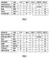
- FIG. 2is a truth table illustrating a command set corresponding to the memory device shown in FIG. 1 for implementing burst mode operation in the memory device of FIG. 1 .
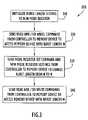
- FIG. 3is a functional flow diagram illustrating the sequence of commands required to perform burst mode in the memory device shown in FIG. 1 .
- FIG. 4is a block diagram of a memory device configured to implement on-the-fly burst mode.
- FIG. 5is a truth table illustrating an example of a command set for implementing on-the-fly burst mode in the memory device shown in FIG. 4 .
- FIG. 6is a functional flow diagram illustrating switching between different burst lengths in successive accesses to the memory device shown in FIG. 4 without re-writing the contents of the mode register.
- Memory device 100includes a command decoder 110 , a mode register 120 , and a memory array 130 .
- Command decoder 110receives operational commands from a controller 140 in the form of three control bits: CS# (chip select), WE# (write enable), and REF# (refresh), where combinations of the values of these control bits correspond to particular commands.
- Memory array 130receives address information for reading and writing via an “Address” input and receives data to be written to the memory array via a “Data In” input. Data read from memory array 130 is supplied on a “Data Out” output.
- the input and output signals sent and received via the Address, Data In, and Data Out linesare typically multi-bit signals (e.g., address and data words).
- Command decoder 110essentially decodes the values of the input control bits to determine the command being sent from controller 140 .
- the truth table shown in FIG. 2provides an example of a command decoding scheme. Specifically, if the CS# bit is at a high level (H), the memory device is deselected (NOP), and no operation is performed regardless of the values of the other control bits.
- the combination of the CS#, WE#, and REF# bits all at a low level (L)specifies that the commanded operation is “Mode Register Set” (MRS).
- MRSMode Register Set
- a mode register set commandis sent from command decoder 110 to mode register 120 , and mode register 120 is loaded with operation code (opcode) data, which can be supplied via the address input (or, optionally, the data input).
- operational parameters that can be set in the mode registermay include the burst length, drive strength, impedance calibration, and read/write latencies.
- command decoder 110sends a read command to memory array 130 , and data is read from memory array 130 beginning at the address indicated via the address input.
- the addressis specified by a three bit bank address (BA) and a twenty-one bit address (A).
- BAbank address
- Atwenty-one bit address
- the combination of the CS# and WE# bits low (L) and the REF# bit high (H)corresponds to the “Write” operation.
- command decoder 110sends a write command to memory array 130 , and data on the data input is written to memory array 130 beginning at the address indicated via the address input.
- the combination of the CS# and REF# bits low (L) and the WE# bit high (H)corresponds to the Auto Refresh (AREF) operation, and auto refresh is performed for the memory bank specified by the bank address.
- burst mode operation using memory device 100is described in connection with the flow chart of FIG. 3 .
- memory device 100requires the contents of mode register 120 to be changed to perform reading or writing at different burst lengths.
- the command set shown in the table of FIG. 2permits the controller to specify a read operation or a write operation, which is carried out according to the burst length setting in the mode register 120 .
- the burst length setting in mode register 120can be set to a default value N (operation 310 ).
- mode register 120Until the contents of mode register 120 are altered, subsequent read and write commands sent from controller 140 to memory device 100 cause memory array 130 to be accessed with the burst length N as specified by the mode register settings (operation 320 ). If memory device 100 is to be accessed using a different burst length (e.g., burst length M), controller 140 must send a mode register set command to memory device 100 together with new mode register settings in order to change the burst length from N to M (operation 330 ). After re-writing the contents of mode register 120 , controller 140 can then send read or write commands to memory device 100 to access memory array 130 using a burst length M (operation 340 ).
- burst length Me.g., burst length M
- the burst lengthis initially set to four (i.e., four data words) and a page burst is required, it is necessary first to perform a mode register set operation to change the burst length setting contents of the mode register. This requirement results in complexity in the controller as well as a delay in implementing the page burst.
- a memory device 400can implement on-the-fly burst mode without having to change the contents of the mode register.
- the designation “on-the-fly”refers to the capability to switch from accessing the memory device with one burst length to accessing the memory device with different burst length without changing the contents of the mode register that controls how the memory device is accessed.
- the architecture depicted in FIG. 4is a conceptual diagram illustrating major functional units, and does not necessarily illustrate physical relationships.
- Memory device 400can be, for example, a dynamic random access memory (DRAM), such as a double data rate (DDR) synchronous DRAM (SDRAM), or a reduced latency DRAM (RLDRAM).
- DRAMdynamic random access memory
- DDRdouble data rate
- SDRAMdouble data rate synchronous DRAM
- RLDRAMreduced latency DRAM
- memory device 400can represent virtually any type of memory device in which burst mode operation may be applicable, and the invention is not limited to any particular type of memory device.
- Memory device 400includes a command decoder 410 , a mode register 420 , a memory array 430 and an address latch/counter 440 .
- Command decoder 410receives operational commands from a controller 450 in the form of the three control bits previous described: CS#, WE#, and REF#, where combinations of the values of bits correspond to particular commands.
- Mode register 420stores memory access parameters, such as the burst length associated with a normal read or write operation, drive strength, calibration, and latency. Optionally, the burst length associated with a burst read or write operation may also be stored in mode register 420 , as will be described in greater detail below.
- Address latch/counter 440receives the address input and supplies address information for reading and writing to memory array 430 .
- Memory array 430also receives data to be written to the memory via the data input (Data In). Data read from memory array 430 is supplied on the data output (Data Out).
- the command decoder 410 , mode register 420 and address/latch counter 440can be distinct units or modules or can be implemented jointly in a common operational module or unit, and, optionally, at least certain operations performed by these modules can be performed via software.
- Controller 450includes a memory management module 460 and a command generator module 470 . These modules may be implemented in software, hardware or combinations thereof and may be implemented as a single operational module, unit or process, or as a plurality of distinct modules, units or processes.
- Memory management module 460is responsible for managing control of memory device 400 (e.g., determining the sequence of commands that must be sent to the memory device to store and retrieve data efficiently, controlling memory access parameters, etc.) based on the memory needs of the processor or system that the memory device is supporting. Those skilled in the art will recognize that the particular configuration of memory management module 460 depends upon the system architecture and the requirements of the types of applications to be handled by the system.
- the command generator module 470essentially generates the command signal or control bits that are sent to memory device 400 to carry out certain operations based on the operations specified by memory management module 460 . An example of a command set generated by command generator module 470 will be described below in detail.
- Command decoder 410decodes the values of the input control bits to determine the command being sent from controller 450 .
- the truth table shown in FIG. 5provides an example of a command decoding scheme that enables a burst mode to be implemented without having to re-write the contents of mode register 420 (i.e., the memory access parameters).
- the commands and corresponding operationscan be summarized as follows. If the CS# bit is high (H) and the WE# and REF# bits are low (L), the memory device is deselected (NOP), and no operation is performed. The combination of the CS#, WE#, and REF# bits all low (L) specifies that the commanded operation is Mode Register Set (MRS). In this case, a Mode Register Set Command is sent from command decoder 410 to mode register 420 , and mode register 420 is loaded with operation code (opcode) data, which can be supplied via the Address input (or, optionally, the data input).
- opcodeoperation code
- command decoder 410sends a read command to memory array 430 , and data is read from memory array 430 beginning at the address indicated via the address input, and the data is supplied as output at the data output.
- the addresscan be specified by a three bit bank address (BA) and a twenty-one bit address (A).
- BAbank address
- Atwenty-one bit address
- the combination of the CS# and WE# bits low (L), and the REF# bit high (H)corresponds to the “Write” operation.
- Command decoder 410sends a write command to memory array 430 , and data received via the data input is written to memory array 330 beginning at the address indicated via the address input.
- the read and write operationsare performed in accordance with the burst length setting stored in mode register 420 .
- the combination of the CS# and REF# bits low (L) and the WE# bit high (H)corresponds to the Auto Refresh (AREF) operation.
- the set of operational commandscan be expanded to include a “Read Burst” operation and a “Write Burst” operation.
- the combination of the CS#, WE#, and REF# bits high (H)can correspond to the Read Burst operation (READB)
- the combination of the CS# and REF# bits high (H) and the WE# bit low (L)can correspond to the Write Burst operation (WRITEB), as shown in the table of FIG. 5
- the combination of the CS# and WE# bits high (H) and the REF# bit low (L)can correspond to a “Terminate” operation (TERM).
- the term memory access command(s)refers to the commands used for writing to or reading from the memory array.
- the regular read or write commandcan be a first memory access command
- a read burst or write burst commandcan be a second memory access command.
- the burst length associated with the read burst and write burst operationscan have a value different from the burst length specified by the mode register for normal read and write operations.
- the read burst and write burst operationscan be configured such that a full page burst is executed in response to a read burst or write burst command.
- the burst length associated with the read burst and write burst operationscan have a fixed value (e.g., a full page) or can be programmable.
- One implementation of a programmable burst mode burst lengthis to allocate certain bits in the mode register that specify the burst length in much the same manner as the burst length of a regular read or write operation, such that the burst mode burst length can be changed with an appropriate mode register set command. Note that, even in this configuration, once the burst lengths associated with the regular and burst access operations are set in the mode register, it is possible to switch between burst mode and non-burst mode (regular) access of the memory device on the fly without altering the contents of the mode register.
- command decoder 410when a read burst operation is specified by the control bits, command decoder 410 sends a read burst (READB) command to memory array 430 .
- the read burst commandis also received by address latch/counter 440 , which latches the input start address and performs a counter function that supplies a sequence of addresses to memory array 430 beginning with the start address in accordance with the burst mode burst length, such that a succession of words is read from memory array 430 and supplied on the data output.
- command decoder 410sends a write burst (WRITEB) command to memory array 430 .
- WRITEBwrite burst
- the write burst commandis also received by address latch/counter 440 , which latches the input start address and performs a counter function that supplies a sequence of addresses to memory array 430 beginning with the start address in accordance with the burst mode burst length, such that a succession of words is written from the data input to memory array 430 .
- address latch/counter 440provides a conceptual sense of accessing a sequence of addresses based off a start address in a burst mode. It will be understood, however, that the burst mode address sequencing can be implemented in any of a variety of ways (e.g., in memory array control logic), and the invention is not limited to implementations involving a separate latch/counter mechanism, such as that shown conceptually in FIG. 4 .
- the read burst and write burst commandsare separate and distinct commands from the read and write commands.
- the burst length associated with the read burst and write burst commandsis independent of the burst length setting in the mode register associated with the read and write commands. This expanded set of commands permits switching between regular access (i.e., that performed by the read and write operations) and burst mode without necessitating any changes to the mode register settings, simply by having the controller send (via the control bits) read or write commands versus read burst or write burst commands.
- the flow diagram shown in FIG. 6illustrates the capability to switch between two different memory access burst lengths in the absence of the requirement to re-write the contents of the mode register.
- the burst length setting in mode register 420 associated with the read and write operationscan be set to a default value N (operation 610 ).
- the burst length M associated with the read burst and write burst operationscan have a fixed value (e.g., full page) such that the read burst and write burst commands are always carried out with the same burst length.
- the burst length associated with the read burst and write burst operationscan be configurable or programmable in much the same manner as the burst length associated with the read and write operations (e.g., a settable value in the mode register).
- Read and write commands sent from controller 440 to memory device 400cause memory array 430 to be accessed with the burst length N as specified by mode register 420 (operation 620 ).
- controller 440sends the control bits associated with the read burst or write burst commands to command decoder 410 (operation 620 ).
- No mode register set commandis required between a read (or write) command and a successive read burst (or write burst) command and vice versa.
- the controllersimply has to send one of the burst commands rather than the normal read or write command to effect the page burst.
- on-the-fly burst modecan be appreciated by considering some practical examples.
- one factor to consideris the smallest increment of data that needs to be transferred in order to get the data granularity required by the processor.
- the required granularitycan generally be achieved by setting a default burst length to a low level, such as four data words.
- setting the base burst length to a low levelplaces a significant burden on the controller, because when large amounts of data must be accessed, the controller must keep track of a considerable number of items and more states are required in the controller.
- either the controllermust be designed to send a sequence of commands to write in bursts of four words at a time or have the complexity to adjust the contents of the mode register to change the burst length before beginning the page burst (the former option may be unacceptably slow in many instances, since the initial word accessed from each command requires a full row cycle time (tRC) whereas subsequent words in a burst can typically be accessed in a fraction of the tRC).
- tRCrow cycle time
- the controllercan have the desired data granularity but still have the capability to read or write large quantities of data without incurring the complexity and time penalty of re-writing the mode register such that, even if the basic write command is set to a burst length of four, the write burst command can be set to full page, and a page burst can be accomplished with one command without resetting the mode register.
- burst length associated with read burst and write burst commandsis configurable or programmable, even greater flexibility is possible. For example, if at a certain time, it is advantageous to switch between burst lengths of four and eight, then these two values can be assigned to the respective burst lengths associated with the non-burst read/write commands and the read burst/write burst commands. If, at another time, it is advantageous to switch between burst lengths of sixteen and full page, then these two values can be assigned to the respective burst lengths to achieve rapid on-the-fly switching between these two burst lengths.
- the terminate commandprovides additional flexibility to the on-the-fly burst mode scheme. Specifically, the terminate command causes a burst read or burst write that is in progress to be immediately terminated on the fly. Thus, for example, if the burst length for the burst mode commands is set to large value, such as the full page, burst accesses of arbitrarily shorter lengths can be achieved by appropriately selecting the timing of a subsequent terminate command. Consequently, the combination of the read and write burst commands and the terminate command effectively permits a variable length burst mode without having to re-write the contents of the mode register to select the desired burst length. This functionality is particularly useful where the desired burst length varies frequently among a number of values.
- the on-the-fly burst mode techniquecan be implemented using any control or command scheme that includes signals which permit switching between memory access with one burst length and memory access with another burst length without requiring stored parameters that control access to the memory to be changed or reset with a separate command from the controller.
- the described on-the-fly burst mode techniquealso is not limited to any particular memory array architecture or addressing scheme. Thus, for example, the technique is equally applicable in memory devices that increment parts of the address for write and read commands.
- the on-the-fly burst mode techniquepermits real time use of full page burst mode without changing mode register. This results in few controller states and less complexity in the controller. Using a small burst length, the controller must cache much more data as it goes through its states to perform several small accesses, thereby requiring a significant cache size. Using on-the-fly full page burst mode offers the possibility of reducing the controller cache size. Further, switching between different burst lengths can be performed more quickly, because no operations need to be carried out to adjust the mode register. Additionally, fewer commands need to be driven over an external bust to the memory device, resulting in power savings.
Landscapes
- Engineering & Computer Science (AREA)
- Theoretical Computer Science (AREA)
- Physics & Mathematics (AREA)
- General Engineering & Computer Science (AREA)
- General Physics & Mathematics (AREA)
- Dram (AREA)
Abstract
Description
Claims (26)
Priority Applications (1)
| Application Number | Priority Date | Filing Date | Title |
|---|---|---|---|
| US10/747,277US7111143B2 (en) | 2003-12-30 | 2003-12-30 | Burst mode implementation in a memory device |
Applications Claiming Priority (1)
| Application Number | Priority Date | Filing Date | Title |
|---|---|---|---|
| US10/747,277US7111143B2 (en) | 2003-12-30 | 2003-12-30 | Burst mode implementation in a memory device |
Publications (2)
| Publication Number | Publication Date |
|---|---|
| US20050144371A1 US20050144371A1 (en) | 2005-06-30 |
| US7111143B2true US7111143B2 (en) | 2006-09-19 |
Family
ID=34700721
Family Applications (1)
| Application Number | Title | Priority Date | Filing Date |
|---|---|---|---|
| US10/747,277Expired - LifetimeUS7111143B2 (en) | 2003-12-30 | 2003-12-30 | Burst mode implementation in a memory device |
Country Status (1)
| Country | Link |
|---|---|
| US (1) | US7111143B2 (en) |
Cited By (45)
| Publication number | Priority date | Publication date | Assignee | Title |
|---|---|---|---|---|
| US20060233030A1 (en)* | 2005-04-14 | 2006-10-19 | Micron Technology, Inc. | System and method for enhanced mode register definitions |
| US20080159023A1 (en)* | 2006-12-27 | 2008-07-03 | Mun Phil Park | Semiconductor memory device with a fixed burst length having column control unit |
| US20090063731A1 (en)* | 2007-09-05 | 2009-03-05 | Gower Kevin C | Method for Supporting Partial Cache Line Read and Write Operations to a Memory Module to Reduce Read and Write Data Traffic on a Memory Channel |
| US20090063730A1 (en)* | 2007-08-31 | 2009-03-05 | Gower Kevin C | System for Supporting Partial Cache Line Write Operations to a Memory Module to Reduce Write Data Traffic on a Memory Channel |
| US20090063785A1 (en)* | 2007-08-31 | 2009-03-05 | Gower Kevin C | Buffered Memory Module Supporting Double the Memory Device Data Width in the Same Physical Space as a Conventional Memory Module |
| US20090190429A1 (en)* | 2008-01-24 | 2009-07-30 | Brittain Mark A | System to Provide Memory System Power Reduction Without Reducing Overall Memory System Performance |
| US7770077B2 (en) | 2008-01-24 | 2010-08-03 | International Business Machines Corporation | Using cache that is embedded in a memory hub to replace failed memory cells in a memory subsystem |
| US7818497B2 (en) | 2007-08-31 | 2010-10-19 | International Business Machines Corporation | Buffered memory module supporting two independent memory channels |
| US7840748B2 (en) | 2007-08-31 | 2010-11-23 | International Business Machines Corporation | Buffered memory module with multiple memory device data interface ports supporting double the memory capacity |
| US7861014B2 (en) | 2007-08-31 | 2010-12-28 | International Business Machines Corporation | System for supporting partial cache line read operations to a memory module to reduce read data traffic on a memory channel |
| US7865674B2 (en) | 2007-08-31 | 2011-01-04 | International Business Machines Corporation | System for enhancing the memory bandwidth available through a memory module |
| US7925825B2 (en) | 2008-01-24 | 2011-04-12 | International Business Machines Corporation | System to support a full asynchronous interface within a memory hub device |
| US7925824B2 (en) | 2008-01-24 | 2011-04-12 | International Business Machines Corporation | System to reduce latency by running a memory channel frequency fully asynchronous from a memory device frequency |
| US7925826B2 (en) | 2008-01-24 | 2011-04-12 | International Business Machines Corporation | System to increase the overall bandwidth of a memory channel by allowing the memory channel to operate at a frequency independent from a memory device frequency |
| US7930470B2 (en) | 2008-01-24 | 2011-04-19 | International Business Machines Corporation | System to enable a memory hub device to manage thermal conditions at a memory device level transparent to a memory controller |
| US8019919B2 (en) | 2007-09-05 | 2011-09-13 | International Business Machines Corporation | Method for enhancing the memory bandwidth available through a memory module |
| US8082482B2 (en) | 2007-08-31 | 2011-12-20 | International Business Machines Corporation | System for performing error correction operations in a memory hub device of a memory module |
| US8086936B2 (en) | 2007-08-31 | 2011-12-27 | International Business Machines Corporation | Performing error correction at a memory device level that is transparent to a memory channel |
| US8140936B2 (en) | 2008-01-24 | 2012-03-20 | International Business Machines Corporation | System for a combined error correction code and cyclic redundancy check code for a memory channel |
| US20120201088A1 (en)* | 2006-07-31 | 2012-08-09 | Google Inc. | Memory circuit system and method |
| US8566556B2 (en) | 2006-02-09 | 2013-10-22 | Google Inc. | Memory module with memory stack and interface with enhanced capabilities |
| US8566516B2 (en) | 2006-07-31 | 2013-10-22 | Google Inc. | Refresh management of memory modules |
| US8615679B2 (en) | 2005-06-24 | 2013-12-24 | Google Inc. | Memory modules with reliability and serviceability functions |
| US8619452B2 (en) | 2005-09-02 | 2013-12-31 | Google Inc. | Methods and apparatus of stacking DRAMs |
| US8631193B2 (en) | 2008-02-21 | 2014-01-14 | Google Inc. | Emulation of abstracted DIMMS using abstracted DRAMS |
| US8631220B2 (en) | 2006-07-31 | 2014-01-14 | Google Inc. | Adjusting the timing of signals associated with a memory system |
| US8667312B2 (en) | 2006-07-31 | 2014-03-04 | Google Inc. | Performing power management operations |
| US8671244B2 (en) | 2006-07-31 | 2014-03-11 | Google Inc. | Simulating a memory standard |
| US8675429B1 (en) | 2007-11-16 | 2014-03-18 | Google Inc. | Optimal channel design for memory devices for providing a high-speed memory interface |
| US8705240B1 (en) | 2007-12-18 | 2014-04-22 | Google Inc. | Embossed heat spreader |
| US8710862B2 (en) | 2009-06-09 | 2014-04-29 | Google Inc. | Programming of DIMM termination resistance values |
| US8751732B2 (en) | 2006-10-05 | 2014-06-10 | Google Inc. | System and method for increasing capacity, performance, and flexibility of flash storage |
| US8762675B2 (en) | 2008-06-23 | 2014-06-24 | Google Inc. | Memory system for synchronous data transmission |
| US8760936B1 (en) | 2006-11-13 | 2014-06-24 | Google Inc. | Multi-rank partial width memory modules |
| US8773937B2 (en) | 2005-06-24 | 2014-07-08 | Google Inc. | Memory refresh apparatus and method |
| US8796830B1 (en) | 2006-09-01 | 2014-08-05 | Google Inc. | Stackable low-profile lead frame package |
| US8819356B2 (en) | 2008-07-25 | 2014-08-26 | Google Inc. | Configurable multirank memory system with interface circuit |
| US8949519B2 (en) | 2005-06-24 | 2015-02-03 | Google Inc. | Simulating a memory circuit |
| US8972673B2 (en) | 2006-07-31 | 2015-03-03 | Google Inc. | Power management of memory circuits by virtual memory simulation |
| US8977806B1 (en) | 2006-10-05 | 2015-03-10 | Google Inc. | Hybrid memory module |
| US9047976B2 (en) | 2006-07-31 | 2015-06-02 | Google Inc. | Combined signal delay and power saving for use with a plurality of memory circuits |
| US9171585B2 (en) | 2005-06-24 | 2015-10-27 | Google Inc. | Configurable memory circuit system and method |
| US9507739B2 (en) | 2005-06-24 | 2016-11-29 | Google Inc. | Configurable memory circuit system and method |
| US9632929B2 (en) | 2006-02-09 | 2017-04-25 | Google Inc. | Translating an address associated with a command communicated between a system and memory circuits |
| US10013371B2 (en) | 2005-06-24 | 2018-07-03 | Google Llc | Configurable memory circuit system and method |
Families Citing this family (10)
| Publication number | Priority date | Publication date | Assignee | Title |
|---|---|---|---|---|
| US7254658B2 (en)* | 2004-06-08 | 2007-08-07 | Arm Limited | Write transaction interleaving |
| US20080059748A1 (en)* | 2006-08-31 | 2008-03-06 | Nokia Corporation | Method, mobile device, system and software for a write method with burst stop and data masks |
| US20080301391A1 (en)* | 2007-06-01 | 2008-12-04 | Jong-Hoon Oh | Method and apparatus for modifying a burst length for semiconductor memory |
| CN101916227B (en)* | 2010-08-13 | 2015-04-01 | 中兴通讯股份有限公司 | RLDRAM SIO storage access control method and device |
| US10025685B2 (en)* | 2015-03-27 | 2018-07-17 | Intel Corporation | Impedance compensation based on detecting sensor data |
| JP2018205859A (en)* | 2017-05-31 | 2018-12-27 | キヤノン株式会社 | Memory controller and control method thereof |
| US10725931B2 (en)* | 2018-08-22 | 2020-07-28 | Western Digital Technologies, Inc. | Logical and physical address field size reduction by alignment-constrained writing technique |
| US11211103B1 (en)* | 2020-08-18 | 2021-12-28 | Micron Technology, Inc. | Burst clock control based on partial command decoding in a memory device |
| JP2022103643A (en)* | 2020-12-28 | 2022-07-08 | ソニーセミコンダクタソリューションズ株式会社 | Memory control device and memory control method |
| KR20240009813A (en)* | 2022-07-14 | 2024-01-23 | 삼성전자주식회사 | Storage modue supporting single serialized write interfacing scheme and operation method thereof |
Citations (3)
| Publication number | Priority date | Publication date | Assignee | Title |
|---|---|---|---|---|
| US5307320A (en)* | 1992-09-23 | 1994-04-26 | Intel Corporation | High integration DRAM controller |
| US5566119A (en)* | 1994-11-10 | 1996-10-15 | Nec Corporation | Synchronous DRAM performing refresh operation a plurality of times in response to each refresh request command |
| US6088760A (en)* | 1997-03-07 | 2000-07-11 | Mitsubishi Semiconductor America, Inc. | Addressing system in a multi-port RAM having main and cache memories |
- 2003
- 2003-12-30USUS10/747,277patent/US7111143B2/ennot_activeExpired - Lifetime
Patent Citations (3)
| Publication number | Priority date | Publication date | Assignee | Title |
|---|---|---|---|---|
| US5307320A (en)* | 1992-09-23 | 1994-04-26 | Intel Corporation | High integration DRAM controller |
| US5566119A (en)* | 1994-11-10 | 1996-10-15 | Nec Corporation | Synchronous DRAM performing refresh operation a plurality of times in response to each refresh request command |
| US6088760A (en)* | 1997-03-07 | 2000-07-11 | Mitsubishi Semiconductor America, Inc. | Addressing system in a multi-port RAM having main and cache memories |
Cited By (57)
| Publication number | Priority date | Publication date | Assignee | Title |
|---|---|---|---|---|
| US7433248B2 (en) | 2005-04-14 | 2008-10-07 | Micron Technology, Inc. | System and method for enhanced mode register definitions |
| US7184327B2 (en)* | 2005-04-14 | 2007-02-27 | Micron Technology, Inc. | System and method for enhanced mode register definitions |
| US20070140022A1 (en)* | 2005-04-14 | 2007-06-21 | Micron Technology, Inc. | System and method for enhanced mode register definitions |
| US20060233030A1 (en)* | 2005-04-14 | 2006-10-19 | Micron Technology, Inc. | System and method for enhanced mode register definitions |
| US9507739B2 (en) | 2005-06-24 | 2016-11-29 | Google Inc. | Configurable memory circuit system and method |
| US8773937B2 (en) | 2005-06-24 | 2014-07-08 | Google Inc. | Memory refresh apparatus and method |
| US9171585B2 (en) | 2005-06-24 | 2015-10-27 | Google Inc. | Configurable memory circuit system and method |
| US8615679B2 (en) | 2005-06-24 | 2013-12-24 | Google Inc. | Memory modules with reliability and serviceability functions |
| US8949519B2 (en) | 2005-06-24 | 2015-02-03 | Google Inc. | Simulating a memory circuit |
| US10013371B2 (en) | 2005-06-24 | 2018-07-03 | Google Llc | Configurable memory circuit system and method |
| US8619452B2 (en) | 2005-09-02 | 2013-12-31 | Google Inc. | Methods and apparatus of stacking DRAMs |
| US8811065B2 (en) | 2005-09-02 | 2014-08-19 | Google Inc. | Performing error detection on DRAMs |
| US9632929B2 (en) | 2006-02-09 | 2017-04-25 | Google Inc. | Translating an address associated with a command communicated between a system and memory circuits |
| US8566556B2 (en) | 2006-02-09 | 2013-10-22 | Google Inc. | Memory module with memory stack and interface with enhanced capabilities |
| US8797779B2 (en) | 2006-02-09 | 2014-08-05 | Google Inc. | Memory module with memory stack and interface with enhanced capabilites |
| US8868829B2 (en)* | 2006-07-31 | 2014-10-21 | Google Inc. | Memory circuit system and method |
| US20120201088A1 (en)* | 2006-07-31 | 2012-08-09 | Google Inc. | Memory circuit system and method |
| US8671244B2 (en) | 2006-07-31 | 2014-03-11 | Google Inc. | Simulating a memory standard |
| US8667312B2 (en) | 2006-07-31 | 2014-03-04 | Google Inc. | Performing power management operations |
| US8631220B2 (en) | 2006-07-31 | 2014-01-14 | Google Inc. | Adjusting the timing of signals associated with a memory system |
| US8972673B2 (en) | 2006-07-31 | 2015-03-03 | Google Inc. | Power management of memory circuits by virtual memory simulation |
| US8566516B2 (en) | 2006-07-31 | 2013-10-22 | Google Inc. | Refresh management of memory modules |
| US9047976B2 (en) | 2006-07-31 | 2015-06-02 | Google Inc. | Combined signal delay and power saving for use with a plurality of memory circuits |
| US8796830B1 (en) | 2006-09-01 | 2014-08-05 | Google Inc. | Stackable low-profile lead frame package |
| US8751732B2 (en) | 2006-10-05 | 2014-06-10 | Google Inc. | System and method for increasing capacity, performance, and flexibility of flash storage |
| US8977806B1 (en) | 2006-10-05 | 2015-03-10 | Google Inc. | Hybrid memory module |
| US8760936B1 (en) | 2006-11-13 | 2014-06-24 | Google Inc. | Multi-rank partial width memory modules |
| US7508731B2 (en)* | 2006-12-27 | 2009-03-24 | Hynix Semiconductor Inc. | Semiconductor memory device with a fixed burst length having column control unit |
| US20080159023A1 (en)* | 2006-12-27 | 2008-07-03 | Mun Phil Park | Semiconductor memory device with a fixed burst length having column control unit |
| US7584308B2 (en)* | 2007-08-31 | 2009-09-01 | International Business Machines Corporation | System for supporting partial cache line write operations to a memory module to reduce write data traffic on a memory channel |
| US8082482B2 (en) | 2007-08-31 | 2011-12-20 | International Business Machines Corporation | System for performing error correction operations in a memory hub device of a memory module |
| US7861014B2 (en) | 2007-08-31 | 2010-12-28 | International Business Machines Corporation | System for supporting partial cache line read operations to a memory module to reduce read data traffic on a memory channel |
| US7840748B2 (en) | 2007-08-31 | 2010-11-23 | International Business Machines Corporation | Buffered memory module with multiple memory device data interface ports supporting double the memory capacity |
| US20090063730A1 (en)* | 2007-08-31 | 2009-03-05 | Gower Kevin C | System for Supporting Partial Cache Line Write Operations to a Memory Module to Reduce Write Data Traffic on a Memory Channel |
| US20090063785A1 (en)* | 2007-08-31 | 2009-03-05 | Gower Kevin C | Buffered Memory Module Supporting Double the Memory Device Data Width in the Same Physical Space as a Conventional Memory Module |
| US8086936B2 (en) | 2007-08-31 | 2011-12-27 | International Business Machines Corporation | Performing error correction at a memory device level that is transparent to a memory channel |
| US7865674B2 (en) | 2007-08-31 | 2011-01-04 | International Business Machines Corporation | System for enhancing the memory bandwidth available through a memory module |
| US7899983B2 (en) | 2007-08-31 | 2011-03-01 | International Business Machines Corporation | Buffered memory module supporting double the memory device data width in the same physical space as a conventional memory module |
| US7818497B2 (en) | 2007-08-31 | 2010-10-19 | International Business Machines Corporation | Buffered memory module supporting two independent memory channels |
| US20090063731A1 (en)* | 2007-09-05 | 2009-03-05 | Gower Kevin C | Method for Supporting Partial Cache Line Read and Write Operations to a Memory Module to Reduce Read and Write Data Traffic on a Memory Channel |
| US7558887B2 (en) | 2007-09-05 | 2009-07-07 | International Business Machines Corporation | Method for supporting partial cache line read and write operations to a memory module to reduce read and write data traffic on a memory channel |
| US8019919B2 (en) | 2007-09-05 | 2011-09-13 | International Business Machines Corporation | Method for enhancing the memory bandwidth available through a memory module |
| US8675429B1 (en) | 2007-11-16 | 2014-03-18 | Google Inc. | Optimal channel design for memory devices for providing a high-speed memory interface |
| US8730670B1 (en) | 2007-12-18 | 2014-05-20 | Google Inc. | Embossed heat spreader |
| US8705240B1 (en) | 2007-12-18 | 2014-04-22 | Google Inc. | Embossed heat spreader |
| US7770077B2 (en) | 2008-01-24 | 2010-08-03 | International Business Machines Corporation | Using cache that is embedded in a memory hub to replace failed memory cells in a memory subsystem |
| US8140936B2 (en) | 2008-01-24 | 2012-03-20 | International Business Machines Corporation | System for a combined error correction code and cyclic redundancy check code for a memory channel |
| US7925825B2 (en) | 2008-01-24 | 2011-04-12 | International Business Machines Corporation | System to support a full asynchronous interface within a memory hub device |
| US20090190429A1 (en)* | 2008-01-24 | 2009-07-30 | Brittain Mark A | System to Provide Memory System Power Reduction Without Reducing Overall Memory System Performance |
| US7925824B2 (en) | 2008-01-24 | 2011-04-12 | International Business Machines Corporation | System to reduce latency by running a memory channel frequency fully asynchronous from a memory device frequency |
| US7925826B2 (en) | 2008-01-24 | 2011-04-12 | International Business Machines Corporation | System to increase the overall bandwidth of a memory channel by allowing the memory channel to operate at a frequency independent from a memory device frequency |
| US7930469B2 (en) | 2008-01-24 | 2011-04-19 | International Business Machines Corporation | System to provide memory system power reduction without reducing overall memory system performance |
| US7930470B2 (en) | 2008-01-24 | 2011-04-19 | International Business Machines Corporation | System to enable a memory hub device to manage thermal conditions at a memory device level transparent to a memory controller |
| US8631193B2 (en) | 2008-02-21 | 2014-01-14 | Google Inc. | Emulation of abstracted DIMMS using abstracted DRAMS |
| US8762675B2 (en) | 2008-06-23 | 2014-06-24 | Google Inc. | Memory system for synchronous data transmission |
| US8819356B2 (en) | 2008-07-25 | 2014-08-26 | Google Inc. | Configurable multirank memory system with interface circuit |
| US8710862B2 (en) | 2009-06-09 | 2014-04-29 | Google Inc. | Programming of DIMM termination resistance values |
Also Published As
| Publication number | Publication date |
|---|---|
| US20050144371A1 (en) | 2005-06-30 |
Similar Documents
| Publication | Publication Date | Title |
|---|---|---|
| US7111143B2 (en) | Burst mode implementation in a memory device | |
| US5966724A (en) | Synchronous memory device with dual page and burst mode operations | |
| US5307320A (en) | High integration DRAM controller | |
| KR102722737B1 (en) | Apparatuses and methods for configurable memory array bank architectures | |
| JP5399442B2 (en) | Memory transaction burst operation and memory device supporting time multiplexed error correction coding | |
| US6546476B1 (en) | Read/write timing for maximum utilization of bi-directional read/write bus | |
| US8019913B2 (en) | Dynamically setting burst length of double data rate memory device by applying signal to at least one external pin during a read or write transaction | |
| US7433248B2 (en) | System and method for enhanced mode register definitions | |
| JP4734580B2 (en) | Enhanced bus turnaround integrated circuit dynamic random access memory device | |
| US6754135B2 (en) | Reduced latency wide-I/O burst architecture | |
| US20120127810A1 (en) | Semiconductor memory device and access method thereof | |
| US7363452B2 (en) | Pipelined burst memory access | |
| US7840744B2 (en) | Rank select operation between an XIO interface and a double data rate interface | |
| US5537564A (en) | Technique for accessing and refreshing memory locations within electronic storage devices which need to be refreshed with minimum power consumption | |
| US20050144372A1 (en) | Memory device controlled with user-defined commands | |
| US6687184B2 (en) | Memory device having selectable clock input and method for operating same | |
| US6574707B2 (en) | Memory interface protocol using two addressing modes and method of operation | |
| JP5204777B2 (en) | Memory device and control method thereof | |
| US6542958B1 (en) | Software control of DRAM refresh to reduce power consumption in a data processing system | |
| US6151273A (en) | Synchronous semiconductor memory device | |
| US6073203A (en) | Method for the continuous readout of a data sequence from a memory | |
| US8010765B2 (en) | Semiconductor memory device and method for controlling clock latency according to reordering of burst data |
Legal Events
| Date | Code | Title | Description |
|---|---|---|---|
| AS | Assignment | Owner name:INFINEON TECNOLOGIES NORTH AMERICA CORP., CALIFORN Free format text:ASSIGNMENT OF ASSIGNORS INTEREST;ASSIGNOR:WALKER, ROBERT;REEL/FRAME:014858/0357 Effective date:20031220 | |
| AS | Assignment | Owner name:INFINEON TECHNOLOGIES AG, GERMANY Free format text:ASSIGNMENT OF ASSIGNORS INTEREST;ASSIGNOR:INFINEON TECHNOLOGIES NORTH AMERICA CORP.;REEL/FRAME:015459/0347 Effective date:20041214 | |
| STCF | Information on status: patent grant | Free format text:PATENTED CASE | |
| AS | Assignment | Owner name:QIMONDA AG, GERMANY Free format text:ASSIGNMENT OF ASSIGNORS INTEREST;ASSIGNOR:INFINEON TECHNOLOGIES AG;REEL/FRAME:023853/0001 Effective date:20060425 | |
| FPAY | Fee payment | Year of fee payment:4 | |
| FPAY | Fee payment | Year of fee payment:8 | |
| AS | Assignment | Owner name:INFINEON TECHNOLOGIES AG, GERMANY Free format text:ASSIGNMENT OF ASSIGNORS INTEREST;ASSIGNOR:QIMONDA AG;REEL/FRAME:035623/0001 Effective date:20141009 | |
| AS | Assignment | Owner name:POLARIS INNOVATIONS LIMITED, IRELAND Free format text:ASSIGNMENT OF ASSIGNORS INTEREST;ASSIGNOR:INFINEON TECHNOLOGIES AG;REEL/FRAME:036877/0513 Effective date:20150708 | |
| MAFP | Maintenance fee payment | Free format text:PAYMENT OF MAINTENANCE FEE, 12TH YEAR, LARGE ENTITY (ORIGINAL EVENT CODE: M1553) Year of fee payment:12 |