US7109952B2 - Light emitting display, light emitting display panel, and driving method thereof - Google Patents
Light emitting display, light emitting display panel, and driving method thereofDownload PDFInfo
- Publication number
- US7109952B2 US7109952B2US10/457,730US45773003AUS7109952B2US 7109952 B2US7109952 B2US 7109952B2US 45773003 AUS45773003 AUS 45773003AUS 7109952 B2US7109952 B2US 7109952B2
- Authority
- US
- United States
- Prior art keywords
- transistor
- light emitting
- signal
- control signal
- switching element
- Prior art date
- Legal status (The legal status is an assumption and is not a legal conclusion. Google has not performed a legal analysis and makes no representation as to the accuracy of the status listed.)
- Expired - Lifetime, expires
Links
Images


Classifications
- G—PHYSICS
- G09—EDUCATION; CRYPTOGRAPHY; DISPLAY; ADVERTISING; SEALS
- G09G—ARRANGEMENTS OR CIRCUITS FOR CONTROL OF INDICATING DEVICES USING STATIC MEANS TO PRESENT VARIABLE INFORMATION
- G09G3/00—Control arrangements or circuits, of interest only in connection with visual indicators other than cathode-ray tubes
- G09G3/20—Control arrangements or circuits, of interest only in connection with visual indicators other than cathode-ray tubes for presentation of an assembly of a number of characters, e.g. a page, by composing the assembly by combination of individual elements arranged in a matrix no fixed position being assigned to or needed to be assigned to the individual characters or partial characters
- G09G3/22—Control arrangements or circuits, of interest only in connection with visual indicators other than cathode-ray tubes for presentation of an assembly of a number of characters, e.g. a page, by composing the assembly by combination of individual elements arranged in a matrix no fixed position being assigned to or needed to be assigned to the individual characters or partial characters using controlled light sources
- G09G3/30—Control arrangements or circuits, of interest only in connection with visual indicators other than cathode-ray tubes for presentation of an assembly of a number of characters, e.g. a page, by composing the assembly by combination of individual elements arranged in a matrix no fixed position being assigned to or needed to be assigned to the individual characters or partial characters using controlled light sources using electroluminescent panels
- G09G3/32—Control arrangements or circuits, of interest only in connection with visual indicators other than cathode-ray tubes for presentation of an assembly of a number of characters, e.g. a page, by composing the assembly by combination of individual elements arranged in a matrix no fixed position being assigned to or needed to be assigned to the individual characters or partial characters using controlled light sources using electroluminescent panels semiconductive, e.g. using light-emitting diodes [LED]
- G09G3/3208—Control arrangements or circuits, of interest only in connection with visual indicators other than cathode-ray tubes for presentation of an assembly of a number of characters, e.g. a page, by composing the assembly by combination of individual elements arranged in a matrix no fixed position being assigned to or needed to be assigned to the individual characters or partial characters using controlled light sources using electroluminescent panels semiconductive, e.g. using light-emitting diodes [LED] organic, e.g. using organic light-emitting diodes [OLED]
- G09G3/3225—Control arrangements or circuits, of interest only in connection with visual indicators other than cathode-ray tubes for presentation of an assembly of a number of characters, e.g. a page, by composing the assembly by combination of individual elements arranged in a matrix no fixed position being assigned to or needed to be assigned to the individual characters or partial characters using controlled light sources using electroluminescent panels semiconductive, e.g. using light-emitting diodes [LED] organic, e.g. using organic light-emitting diodes [OLED] using an active matrix
- G09G3/3233—Control arrangements or circuits, of interest only in connection with visual indicators other than cathode-ray tubes for presentation of an assembly of a number of characters, e.g. a page, by composing the assembly by combination of individual elements arranged in a matrix no fixed position being assigned to or needed to be assigned to the individual characters or partial characters using controlled light sources using electroluminescent panels semiconductive, e.g. using light-emitting diodes [LED] organic, e.g. using organic light-emitting diodes [OLED] using an active matrix with pixel circuitry controlling the current through the light-emitting element
- G09G3/3241—Control arrangements or circuits, of interest only in connection with visual indicators other than cathode-ray tubes for presentation of an assembly of a number of characters, e.g. a page, by composing the assembly by combination of individual elements arranged in a matrix no fixed position being assigned to or needed to be assigned to the individual characters or partial characters using controlled light sources using electroluminescent panels semiconductive, e.g. using light-emitting diodes [LED] organic, e.g. using organic light-emitting diodes [OLED] using an active matrix with pixel circuitry controlling the current through the light-emitting element the current through the light-emitting element being set using a data current provided by the data driver, e.g. by using a two-transistor current mirror
- G09G3/325—Control arrangements or circuits, of interest only in connection with visual indicators other than cathode-ray tubes for presentation of an assembly of a number of characters, e.g. a page, by composing the assembly by combination of individual elements arranged in a matrix no fixed position being assigned to or needed to be assigned to the individual characters or partial characters using controlled light sources using electroluminescent panels semiconductive, e.g. using light-emitting diodes [LED] organic, e.g. using organic light-emitting diodes [OLED] using an active matrix with pixel circuitry controlling the current through the light-emitting element the current through the light-emitting element being set using a data current provided by the data driver, e.g. by using a two-transistor current mirror the data current flowing through the driving transistor during a setting phase, e.g. by using a switch for connecting the driving transistor to the data driver
- G—PHYSICS
- G09—EDUCATION; CRYPTOGRAPHY; DISPLAY; ADVERTISING; SEALS
- G09G—ARRANGEMENTS OR CIRCUITS FOR CONTROL OF INDICATING DEVICES USING STATIC MEANS TO PRESENT VARIABLE INFORMATION
- G09G2300/00—Aspects of the constitution of display devices
- G09G2300/08—Active matrix structure, i.e. with use of active elements, inclusive of non-linear two terminal elements, in the pixels together with light emitting or modulating elements
- G09G2300/0809—Several active elements per pixel in active matrix panels
- G09G2300/0842—Several active elements per pixel in active matrix panels forming a memory circuit, e.g. a dynamic memory with one capacitor
- G09G2300/0852—Several active elements per pixel in active matrix panels forming a memory circuit, e.g. a dynamic memory with one capacitor being a dynamic memory with more than one capacitor
- G—PHYSICS
- G09—EDUCATION; CRYPTOGRAPHY; DISPLAY; ADVERTISING; SEALS
- G09G—ARRANGEMENTS OR CIRCUITS FOR CONTROL OF INDICATING DEVICES USING STATIC MEANS TO PRESENT VARIABLE INFORMATION
- G09G2300/00—Aspects of the constitution of display devices
- G09G2300/08—Active matrix structure, i.e. with use of active elements, inclusive of non-linear two terminal elements, in the pixels together with light emitting or modulating elements
- G09G2300/0809—Several active elements per pixel in active matrix panels
- G09G2300/0842—Several active elements per pixel in active matrix panels forming a memory circuit, e.g. a dynamic memory with one capacitor
- G09G2300/0861—Several active elements per pixel in active matrix panels forming a memory circuit, e.g. a dynamic memory with one capacitor with additional control of the display period without amending the charge stored in a pixel memory, e.g. by means of additional select electrodes
- G—PHYSICS
- G09—EDUCATION; CRYPTOGRAPHY; DISPLAY; ADVERTISING; SEALS
- G09G—ARRANGEMENTS OR CIRCUITS FOR CONTROL OF INDICATING DEVICES USING STATIC MEANS TO PRESENT VARIABLE INFORMATION
- G09G2310/00—Command of the display device
- G09G2310/02—Addressing, scanning or driving the display screen or processing steps related thereto
- G09G2310/0243—Details of the generation of driving signals
- G09G2310/0254—Control of polarity reversal in general, other than for liquid crystal displays
- G09G2310/0256—Control of polarity reversal in general, other than for liquid crystal displays with the purpose of reversing the voltage across a light emitting or modulating element within a pixel
- G—PHYSICS
- G09—EDUCATION; CRYPTOGRAPHY; DISPLAY; ADVERTISING; SEALS
- G09G—ARRANGEMENTS OR CIRCUITS FOR CONTROL OF INDICATING DEVICES USING STATIC MEANS TO PRESENT VARIABLE INFORMATION
- G09G2310/00—Command of the display device
- G09G2310/02—Addressing, scanning or driving the display screen or processing steps related thereto
- G09G2310/0262—The addressing of the pixel, in a display other than an active matrix LCD, involving the control of two or more scan electrodes or two or more data electrodes, e.g. pixel voltage dependent on signals of two data electrodes
- G—PHYSICS
- G09—EDUCATION; CRYPTOGRAPHY; DISPLAY; ADVERTISING; SEALS
- G09G—ARRANGEMENTS OR CIRCUITS FOR CONTROL OF INDICATING DEVICES USING STATIC MEANS TO PRESENT VARIABLE INFORMATION
- G09G2310/00—Command of the display device
- G09G2310/06—Details of flat display driving waveforms
- G—PHYSICS
- G09—EDUCATION; CRYPTOGRAPHY; DISPLAY; ADVERTISING; SEALS
- G09G—ARRANGEMENTS OR CIRCUITS FOR CONTROL OF INDICATING DEVICES USING STATIC MEANS TO PRESENT VARIABLE INFORMATION
- G09G2320/00—Control of display operating conditions
- G09G2320/02—Improving the quality of display appearance
- G09G2320/0223—Compensation for problems related to R-C delay and attenuation in electrodes of matrix panels, e.g. in gate electrodes or on-substrate video signal electrodes
- G—PHYSICS
- G09—EDUCATION; CRYPTOGRAPHY; DISPLAY; ADVERTISING; SEALS
- G09G—ARRANGEMENTS OR CIRCUITS FOR CONTROL OF INDICATING DEVICES USING STATIC MEANS TO PRESENT VARIABLE INFORMATION
- G09G2320/00—Control of display operating conditions
- G09G2320/02—Improving the quality of display appearance
- G09G2320/0233—Improving the luminance or brightness uniformity across the screen
- G—PHYSICS
- G09—EDUCATION; CRYPTOGRAPHY; DISPLAY; ADVERTISING; SEALS
- G09G—ARRANGEMENTS OR CIRCUITS FOR CONTROL OF INDICATING DEVICES USING STATIC MEANS TO PRESENT VARIABLE INFORMATION
- G09G2320/00—Control of display operating conditions
- G09G2320/04—Maintaining the quality of display appearance
- G09G2320/043—Preventing or counteracting the effects of ageing
Definitions
- the present inventionrelates to an organic electroluminescence (EL) light emitting display, a light emitting display panel, and a driving method thereof
- ELorganic electroluminescence
- An organic EL displayis a display that emits light by electrical excitation of fluorescent organic compounds and an image is displayed by driving each of M ⁇ N organic luminescent cells with voltage or current.
- This organic cellincludes an anode, an organic thin film and, a cathode layer.
- the anodemay be formed, for example, of indium tin oxide (ITO) and the cathode may be formed, for example, of a metal.
- the organic thin filmis formed as a multi-layered structure including an emission layer (“EML”), an electron transport layer (“ETL”), and a hole transport layer (“HTL”) so as to increase luminescence efficiency by balancing electron and hole concentrations.
- EMLemission layer
- ETLelectron transport layer
- HTLhole transport layer
- EILelectron injection layer
- HILhole injection layer
- Organic EL displaysthat have such organic luminescent cells are configured as passive matrix configuration or active matrix configuration.
- the active matrix configurationincludes thin film transistors (TFTs) or MOSFETs.
- TFTsthin film transistors
- MOSFETsmetal-oxide-semiconductor field-effect transistors
- In the passive matrix configurationorganic luminescent cells are formed between anode lines and cathode lines that cross each other and the organic luminescent cells are driven by driving the anode and cathode lines.
- each organic luminescent cellis connected to a TFT usually through an ITO electrode and is driven by controlling the gate voltage of the corresponding TFT.
- the active matrix methodmay be classified as a voltage programming method and/or a current programming method depending on the format of signals that are applied to the capacitor so as to maintain the voltage.
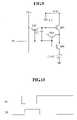
- FIG. 2illustrates a pixel circuit following the conventional voltage programming method for driving an organic EL element.
- FIG. 2illustrates one of the N ⁇ M pixels as a representative.
- a transistor M 1is coupled to an organic EL element OLED to supply the current for emission.
- the current of the transistor M 1is controlled by the data voltage applied through a switching transistor M 2 .
- a capacitor C 1 for maintaining the applied voltage for a predetermined timeis coupled between a source of the transistor M 1 and a gate thereof.
- a gate of the switching transistor M 2is coupled to a scan line S n , and a source thereof is coupled to a data line D m .
- the switching transistor M 2When the switching transistor M 2 is turned on according to a select signal applied to the gate of the switching transistor M 2 , a data voltage from the data line D m is applied to the gate of the transistor M 1 .
- the current I OLEDflows to the switching transistor M 2 depending, for example, on the voltage V GS charged between the gate and the source by the capacitor C 1 , and the organic EL element OLED emits light depending, for example, on the current I OLED .
- the current I OLED flowing to the organic EL element OLEDis expressed in Equation 1.
- I OLEDis a current flowing to the organic EL element OLED
- V GSis a voltage between the source and the gate of the transistor M 1
- V THis a threshold voltage at the transistor M 1
- V DATAis a data voltage
- ⁇is a constant.
- the current corresponding to the applied data voltageis applied to the organic EL element OLED, and the organic EL element emits light in relation to the applied current in the pixel circuit.
- the applied data voltagehas multiple-stage values within a predetermined range so as to display different gray scales.
- the conventional pixel circuit of the voltage programming methodit is difficult for the conventional pixel circuit of the voltage programming method to obtain a wide spectrum of gray scales because of deviations of the threshold voltage V TH of the TFT and electron mobility caused by non-uniformity in the manufacturing process.
- the deviation of the threshold voltage at the TFT caused by the non-uniformity of the manufacturing processis greater than 100 mV, it becomes difficult to express a wide spectrum of gray scales. It is also difficult to express a wide spectrum of gray scales because ⁇ in Equation 1 becomes differentiated due to deviation of the electron mobility.
- the pixel circuit of the current programming methodgenerates uniform display characteristics even when a driving transistor in each pixel has non-uniform voltage-current characteristics.
- FIG. 3shows a conventional pixel circuit of the current programming method for driving an organic EL element, illustrating one of the N ⁇ M pixels as an example.
- a transistor M 1is coupled to an organic EL element OLED to supply the current for emission to the OLED, and the current of the transistor M 1 is set to be controlled by the data current applied through a transistor M 2 .
- an organic EL panelhas substantially uniform characteristics when a programming current source is uniform over the organic EL panel.
- the current I OLED flowing to the organic EL elementis a micro-current, it problematically takes a lot of time to charge the data line in order to control the pixel circuit using the micro-current I DATA .
- the load capacitance of the data lineis 30 pF, it takes several milliseconds to charge the load of the data line with the data current of about several tens to several hundreds nA. Taking a long time to charge the data line is problematic because the charging time is not sufficient (i.e., too long) when considering the data line time of several tens of ⁇ s.
- the present inventionprovides a light emitting device for compensating for a threshold voltage and electron mobility of a transistor for fully charging a data line.
- This inventionseparately provides a light emitting display including a plurality of data lines for transmitting a data current that displays a video signal, a plurality of scan lines for transmitting a select signal, and a plurality of pixel circuits each of which is formed at a pixel generated by the data lines and the scan lines, wherein the pixel circuit comprises a light emitting element for emitting light based on an applied current, a first transistor for supplying a driving current for emitting the light emitting element, a first switching element for transmitting a data signal from the data line associated with the pixel circuit in response to the select signal from the scan line associated with the pixel circuit, a second switching element for diode-connecting the first transistor in response to a first level of a first control signal, a first storage element for storing a first voltage matched with the data current from the first switching element according to the first level of the first control signal, a second storage element coupled between the first storage element and a signal line for supplying the first control signal, for converting the first voltage of
- the second switching elementis coupled between a second main electrode of the first transistor and the control electrode of the first transistor, or between the data line and a second main electrode of the first transistor.
- This inventionseparately provides a method for driving a light emitting display having a pixel circuit including a first switching element for transmitting a data current from a data line in response to a select signal from a scan line, a transistor for outputting a driving current, a first storage element coupled between a first main electrode of the transistor and a control electrode of the transistor, and a light emitting element for emitting light in correspondence to the driving current from the transistor.
- the methodcomprises diode-connecting the transistor using a control signal at a first level, and setting a control electrode voltage of the transistor as a first voltage in correspondence to the data current from the first switching element, interrupting the data current, applying the control signal at a second level to a second end of a second storage element having a first end coupled to a control electrode of the transistor, and changing the control electrode voltage of the transistor to a second voltage through coupling of the first and second storage elements, and applying the driving current output from the transistor to the light emitting element in response to the second voltage.
- This inventionseparately provides a display panel of a light emitting display including a plurality of data lines for transmitting a data current for displaying a video signal, a plurality of scan lines for transmitting a select signal, and a plurality of pixel circuits each of which is generated at a pixel generated by the data line and the scan line.
- the pixel circuitcomprises a light emitting element for emitting light in correspondence to an applied current, a first transistor, having a first main electrode coupled to a first signal line for supplying a power supply voltage, for outputting a current for driving the light emitting element, a first switching element for transmitting a data current from the data line to the first transistor in response to the select signal from the scan line, a second switching element for diode-connecting the first transistor in response to a first level of a first control signal, a third switching element for transmitting a driving current from the transistor to the light emitting element in response to a second control signal; a first storage element coupled between a control electrode of the first transistor and a first main electrode of the first transistor, and a second storage element coupled between the control electrode of the first transistor and a second signal line for supplying the first control signal.
- the display paneloperates in a first interval in which the first transistor is diode-connected by the first control signal at the first level, and the data current is transmitted to the first transistor by the select signal, and a second interval in which the data current is interrupted, the first control signal is changed to a second level, a level variation of the first control signal is reflected to control electrodes of the first transistor according to coupling by the first and second storage elements, and the driving current is transmitted to the light emitting element by the second control signal.
- FIG. 1shows a concept diagram of an organic EL element.
- FIG. 2shows a circuit of a conventional pixel circuit following a voltage driving method.
- FIG. 3shows a circuit of a conventional pixel circuit following a current programming method.
- FIG. 4shows a brief schematic diagram of an organic EL display according to an exemplary embodiment of the present invention.
- FIGS. 5 , 6 , 8 , 9 , 11 , 12 , 13 , 15 , 17 , 19 , 21 , 22 , 23 , and 25respectively show equivalent circuit diagrams of a pixel circuit according to various exemplary embodiments of the present invention.
- FIGS. 7 , 10 , 14 , 16 , 18 , 20 , 24 , and 26respectively show driving waveform diagrams for driving the pixel circuit of FIGS. 6 , 9 , 13 , 15 , 17 , 19 , 23 , and 25 .
- coupling of a first portion to a second portionincludes direct coupling of the first portion to the second portion, and coupling of the first portion to the second portion through a third portion provided between the first and second portions. Also, a reference numeral of a signal applied to a pixel circuit through each scan line is matched with that of the scan line for ease of description.
- FIG. 4shows a brief schematic diagram of an organic EL display according to a first exemplary embodiment of the present invention.
- the organic EL display shown in FIG. 4comprises an organic EL display panel 10 , a scan driver 20 , and a data driver 30 .
- the organic EL display panel 10comprises a plurality of data lines D 1 –D M arranged in the row direction; a plurality of scan lines S 1 –S N and E 1 –E N arranged in the column direction; and a plurality of pixel circuits 11 .
- the data lines D 1 –D Mtransmit the data current for displaying video signals to the pixel circuits 11 .
- a pixel circuit 11is formed at a pixel region defined by two adjacent data lines and two adjacent scan lines. More particularly, for example, a pixel region is defined by the region corresponding to a portion of the space between to two adjacent data lines which overlap a space between scan lines.
- the data driver 30applies the data current to the data lines D 1 –D M
- the scan driver 20respectively applies a select signal and an emit signal to the scan lines S 1 –S N and the scan lines E 1 –E N sequentially.
- FIG. 5a pixel circuit 11 of the organic EL display according to the first exemplary embodiment of the present invention will be described.
- FIG. 5only shows the pixel circuit coupled to the m th data line D m and the n th scan line S n .
- the transistor M 1has a source coupled to the power supply voltage VDD, and a drain coupled to the switch S 3 .
- the gate-source voltage of the transistor M 1is determined in relation to the data current I DATA
- the capacitor C 1is coupled between the gate and the source of the transistor M 1 to help maintain the gate-source voltage of the transistor M 1 for a predetermined time.
- the capacitor C 2is coupled between the scan line S n and the gate of the transistor M 1 to help control the voltage at the gate of the transistor M 1 .
- the switch S 3applies the current flowing to the transistor M 1 to the organic EL element OLED in response to the emit signal provided from the scan line E n .
- the organic EL elementis coupled between the switch S 3 and a reference voltage, and the organic EL element emits light matched with the current flowing to the transistor M 1 , which is substantially equal to the current I OLED applied to the organic EL element OLED when the switch S 3 is closed.
- the switches S 1 , S 2 , and S 3include general switches, and they may further include transistors. Referring to FIGS. 6 and 7 , an exemplary embodiment for realizing the switches S 1 , S 2 , and S 3 as PMOS transistors will be described in detail.
- FIG. 6shows an equivalent circuit of a pixel circuit according to a second exemplary embodiment of the present invention
- FIG. 7shows a driving waveform for driving the pixel circuit of FIG. 6 .
- the pixel circuithas a structure matched with that of the first exemplary embodiment except the transistors M 2 , M 3 , and M 4 are provided instead of the switches S 1 , S 2 , and S 3 in the pixel circuit of FIG. 5 .
- the transistors M 2 , M 3 , and M 4are PMOS transistors, the gates of the transistors M 2 and M 3 are coupled to the scan line S n , and the gate of the transistor M 4 is coupled to the scan line E n .
- the transistors M 2 and M 3are turned off, and the transistor M 4 is turned on.
- the select signal S nis switched to the high level voltage from the low level voltage, the voltage at a common node of the capacitor C 2 and the scan line S n increases by a level rise height of the select signal S n . Therefore, the gate voltage V G of the transistor M 1 increases because of coupling of the capacitors C 1 and C 2 , and the increment is expressed in Equation 5.
- the current I OLED flowing to the transistor M 1is expressed in Equation 6.
- the transistor M 3is turned on because of the emit signal E n , the current I OLED of the transistor M 1 is applied to the organic EL element OLED to emit light.
- the data current I DATAmay be set to be greater than the current I OLED flowing to the organic EL element OLED. That is, because the micro-current flowing to the organic EL element is controlled using the big data current I DATA , a smaller amount of time for charging the data line is sufficient.
- the transistor M 2is driven using the select signal S n from the scan line S n , but a switching error by the transistor M 2 may be generated when the rising time of the select signal S n is varied because of the load of the scan line.
- the select signal S nmay be buffered and applied to the transistor M 2 , which will be described in detail with reference to FIG. 8 .
- FIG. 8shows a pixel circuit according to a third exemplary embodiment of the present invention.
- the pixel circuit according to the third exemplary embodimenthas a similar structure as that of the first exemplary embodiment except for a buffer.
- the bufferincludes four transistors M 5 –M 8 .
- Two of the transistors M 5 and M 7are PMOS transistors, and the other two transistors M 6 and M 8 are NMOS transistors.
- the transistors M 5 and M 6are coupled in series between the power supply voltage VDD and the reference voltage, and a common node of the transistors M 5 and M 6 is coupled to the gates of the transistors M 7 and M 8 .
- a select signal of the (m ⁇ 1) th pixel circuitis input to the gates of the transistors M 5 and M 6 .
- the transistors M 7 and M 8are coupled in series between the power supply voltage VDD and the reference voltage, and an output at the common node of the transistors M 7 and M 8 is applied as a select signal to the gates of the transistors M 2
- the transistor M 6when the select signal input to the gates of the transistors M 5 and M 6 is a high level voltage, the transistor M 6 is turned on, and the signal at a low level voltage is input to the gates of the transistors M 7 and M 8 according to the reference voltage.
- the transistor M 7is turned on according to the signal at a low level voltage, and the signal at a high level voltage is applied as a select signal to the gates of the transistors M 2 and M 3 according to the power supply voltage VDD.
- the select signal input to the gates of the transistors M 5 and M 6is a low level voltage, the transistor M 5 is turned on, and the signal at a high level signal is input to the gates of the transistors M 7 and M 8 according to the power supply voltage VDD.
- the transistor M 8is turned on according to the signal at a high level voltage, and the signal at a low level voltage is applied as a select signal to the gates of the transistors M 2 an M 3 according to the reference voltage.
- the rising time of the select signal at all the pixelsbecomes substantially, and possibly completely, identical, thereby reducing an influence of switching errors of the transistor M 2 .
- an additional scan line E n for transmitting the emit signal E nis used to control the driving of the switch S 3 and/or the transistor M 4 .
- the driving of the switch S 3 or the transistor M 4may be controlled using the select signal S n from the scan line S n without using the additional scan line E n , which will be described in detail with reference to FIGS. 9 and 10 .
- FIG. 9shows a pixel circuit according to a fourth exemplary embodiment of the present invention
- FIG. 10shows a driving waveform for driving the pixel circuit of FIG. 9 .
- the pixel circuit according to the fourth exemplary embodimenthas a similar structure as that of the pixel circuit of FIG. 6 , except that a scan line E n is not provided and the type and coupling state of the transistor M 4 are different.
- the transistor M 4is an NMOS transistor, and the gate of the transistor M 3 is coupled to the scan line S n rather than the scan line E n .
- the select signal S nbecomes a high level voltage, the transistor M 4 is turned on, and the current I OLED output from the transistor M 1 is transmitted to the organic EL element.
- the aperture ratio of the pixelis increased.
- the transistor M 3is coupled between the drain and the gate of the transistor M 1 , thereby, diode-connecting the transistor M 1 .
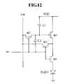
- the transistor M 3it is possible for the transistor M 3 to be coupled between the drain of the transistor M 1 and the data line D m . This arrangement will be described in detail with reference to FIGS. 11 and 12 .
- FIGS. 11 and 12respectively show a pixel circuit according to fifth and sixth exemplary embodiments of the present invention.
- the pixel circuit according to the fifth exemplary embodimenthas a similar structure as that of the pixel circuit of FIG. 6 except for the coupling state of the transistor M 3 .
- the transistor M 3is coupled between the data line D m and the drain of the transistor M 1 , and it drives the pixel circuit using the driving waveform of FIG. 7 .
- the select signal S n from the scan line S nis a low level voltage
- the transistors M 2 and M 3are concurrently turned on, and accordingly, the gate and the drain of the transistor M 1 are coupled. That is, similar to the pixel circuit of FIG. 6 , the transistor M 1 is diode-connected when the select signal S n is a low level voltage.
- the voltage at the gate of the transistor M 1may be influenced when the transistor M 3 is turned off.
- the gate voltage of the transistor M 1is less influenced when the transistor M 3 is turned off.
- the pixel circuit according to a sixth exemplary embodimenthas a structure similar to the pixel circuit of FIG. 9 except that the transistor M 3 is coupled between the data line D m and the drain of the transistor M 1 .
- the scan line S nis coupled to the gates of the transistors M 2 and M 3 .
- the scan line S nit is possible for the scan line S n to only be coupled to the gate of the transistor M 2 . This arrangement will be described in detail with reference to FIGS. 13 through 16 .
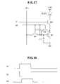
- FIGS. 13 and 15respectively show a pixel circuit according to seventh and eighth exemplary embodiments of the present invention
- FIGS. 14 and 16respectively show a driving waveform diagram for driving the pixel circuits of FIGS. 13 and 15 .
- the pixel circuit according to the seventh exemplary embodimenthas a similar structure as that of the pixel circuit of FIG. 6 except for the coupling state of the transistor M 3 and the capacitor C 2 .
- the gate of the transistor M 3is coupled to an additional scan line B n
- the capacitor C 2is coupled between the gate of the transistor M 1 and the scan line B n .
- a boost signal B n from the scan line B nbecomes a low level voltage before the select signal S n becomes a low level voltage, and it becomes a high level voltage after the select signal S n becomes a high level voltage.
- the transistor M 2is turned off, a voltage at a common node of the capacitor C 2 and the scan line B n increases by the level rising height of the boost signal B n . Therefore, the gate voltage V G of the transistor M 1 increases by the increment of Equation 5 according to the coupling of the capacitors C 1 and C 2 , and the current I OLED of Equation 7 is applied to the organic EL element OLED.
- the other operations of the pixel circuit of FIG. 13are matched with those of the pixel circuit of FIG. 6 .
- the scan line S nis coupled only to the gate of the transistor M 2 to reduce the load of the scan line S n , the rising time of the select signal S n becomes uniform over the whole panel. Also, in the seventh exemplary embodiment, the influence of switching errors of the transistor M 2 is reduced because the gate node of the transistor M 2 is boosted after the transistor M 2 is turned off.
- the scan line E nis removed from the pixel circuit of FIG. 13 and the gate of the transistor M 4 is coupled to the scan line B n to thereby configure a pixel circuit according to the eighth exemplary embodiment.
- the transistor M 4is an NMOS transistor, that is, the transistor M 4 is an opposite type of the transistor in relation to transistor M 3 .
- the emit signal E nis removed from the driving waveform of FIG. 14 .
- the boost signal B nbecomes a high level voltage to boost the gate voltage of the transistor M 2
- the transistor M 4is turned on. Therefore, the gate voltage of the transistor M 2 is boosted, and accordingly, the current I OLED output from the transistor M 1 is applied to the organic EL element OLED to emit light.
- the transistors M 1 -M 3are PMOS transistors, but they may also be NMOS transistors, which will be described with reference to FIGS. 17 through 26 .
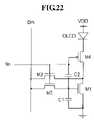
- FIGS. 17 , 19 , 21 , 22 , 23 , and 25respectively show an equivalent circuit diagram of a pixel circuit according to ninth through fourteenth exemplary embodiments
- FIGS. 18 , 20 , 24 , and 26respectively show a driving waveform for driving the pixel circuit of FIGS. 17 , 19 , 23 , and 25 .
- the transistors M 1 –M 4are NMOS transistors in the ninth exemplary embodiment, and their coupling state is symmetric with the pixel circuit of FIG. 6 .
- the transistor M 2is coupled between the data line D m and the gate of the transistor M 1 , and the gate thereof being coupled to the scan line S n .
- the transistor M 3is coupled between the drain and the gate of the transistor M 1 , and the gate thereof being coupled to the scan line S n .
- the source of the transistor M 1is coupled to the reference voltage, and the drain thereof is coupled to the organic EL element OLED.
- the capacitor C 1is coupled between the gate and the source of the transistor M 1 , and the organic EL element is coupled between the transistor M 4 and the power supply voltage VDD.
- the gate of the transistor M 4is coupled to the scan line E n .
- the select signal S n and the emit signal E n for driving the pixel circuit of FIG. 17have an inverse format of the signals S n and E n shown in FIG. 7 , as shown in FIG. 18 . Since a detailed operation of the pixel circuit of FIG. 17 may be easily understood from the description of the second exemplary embodiment, no further description will be provided.
- the transistors M 1 , M 2 , and M 3are NMOS transistors
- the transistor M 4is a PMOS transistor
- their coupling stateis symmetric with that of the pixel circuit of FIG. 9 .
- the select signal S n for driving the transistors M 2 , M 3 , and M 4has an inverse format of the select signal S n of FIG. 10 .
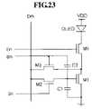
- NMOS transistorsare used for the transistors M 1 –M 4 in the pixel circuit of FIG. 13 .
- the driving waveforms S n , B n , and E n for driving the pixel circuit of FIG. 23respectively have an inverse format of those S n , B n , and E n of FIG. 14 .
- NMOS transistorsare used for the transistors M 1 , M 2 , and M 3
- a PMOS transistoris used for the transistor M 4 in the pixel circuit of FIG. 15 .
- the driving waveforms S n and B n for driving the pixel circuit of FIG. 25respectively have an inverse format of those S n and B n of FIG. 16 .
- the current flowing to the organic EL elementcan be controlled using a large data current, the data line can be fully charged during a single line time frame. Further, deviations of threshold voltages of transistors and deviations of mobility are compensated in the current flowing to the organic EL element, and a light emitting display of high resolution and wide screen can be realized.
Landscapes
- Engineering & Computer Science (AREA)
- Physics & Mathematics (AREA)
- Computer Hardware Design (AREA)
- General Physics & Mathematics (AREA)
- Theoretical Computer Science (AREA)
- Control Of Indicators Other Than Cathode Ray Tubes (AREA)
- Control Of El Displays (AREA)
- Electroluminescent Light Sources (AREA)
- Shift Register Type Memory (AREA)
Abstract
Description
where IOLEDis a current flowing to the organic EL element OLED, VGSis a voltage between the source and the gate of the transistor M1, VTHis a threshold voltage at the transistor M1, VDATAis a data voltage, and β is a constant.
- where VGSis a voltage between the source and the gate of the transistor M1, VTHis a threshold voltage at the transistor M1, and β is a constant.
where β is a constant, and VTHis a threshold voltage at the transistor M1.
where C1and C2are the capacitances of the capacitors C1 and C2, respectively.
Claims (21)
Applications Claiming Priority (4)
| Application Number | Priority Date | Filing Date | Title |
|---|---|---|---|
| KR2002-32676 | 2002-06-11 | ||
| KR20020032676 | 2002-06-11 | ||
| KR2003-17838 | 2003-03-21 | ||
| KR10-2003-0017838AKR100502926B1 (en) | 2002-06-11 | 2003-03-21 | Light emitting display device and display panel and driving method thereof |
Publications (2)
| Publication Number | Publication Date |
|---|---|
| US20030227262A1 US20030227262A1 (en) | 2003-12-11 |
| US7109952B2true US7109952B2 (en) | 2006-09-19 |
Family
ID=29714409
Family Applications (1)
| Application Number | Title | Priority Date | Filing Date |
|---|---|---|---|
| US10/457,730Expired - LifetimeUS7109952B2 (en) | 2002-06-11 | 2003-06-10 | Light emitting display, light emitting display panel, and driving method thereof |
Country Status (3)
| Country | Link |
|---|---|
| US (1) | US7109952B2 (en) |
| JP (1) | JP4195337B2 (en) |
| CN (1) | CN1326108C (en) |
Cited By (47)
| Publication number | Priority date | Publication date | Assignee | Title |
|---|---|---|---|---|
| US20040207617A1 (en)* | 2003-03-27 | 2004-10-21 | Shoichiro Matsumoto | Display circuit |
| US20040252085A1 (en)* | 2003-05-16 | 2004-12-16 | Semiconductor Energy Laboratory Co., Ltd. | Display device |
| US20050024351A1 (en)* | 2003-06-20 | 2005-02-03 | Keiichi Sano | Light emitting device and display device |
| US20050052366A1 (en)* | 2003-09-08 | 2005-03-10 | Keum-Nam Kim | Circuit and method for driving pixel of organic electroluminescent display |
| US20050099412A1 (en)* | 2003-11-11 | 2005-05-12 | Seiko Epson Corporation | Pixel circuit, method of driving the same, and electronic apparatus |
| US20050116903A1 (en)* | 2003-11-29 | 2005-06-02 | Dong-Yong Shin | Display panel, light emitting display device using the same, and driving method thereof |
| US20050140605A1 (en)* | 2003-11-24 | 2005-06-30 | Jin-Tae Jung | Image display device and driving method thereof |
| US20050259051A1 (en)* | 2004-05-20 | 2005-11-24 | Samsung Electronics Co., Ltd | Display device and driving method thereof |
| US20060055651A1 (en)* | 2004-08-24 | 2006-03-16 | Tohoku Pioneer Corporation | Light emitting display device, electronic equipment into which the same device is loaded, and drive method of the light emitting display device |
| US20060077194A1 (en)* | 2004-10-08 | 2006-04-13 | Jeong Jin T | Pixel circuit and light emitting display comprising the same |
| US20060103322A1 (en)* | 2004-11-17 | 2006-05-18 | Lg.Philips Lcd Co., Ltd. | Apparatus and method for driving organic light-emitting diode |
| US20060139263A1 (en)* | 2004-12-24 | 2006-06-29 | Choi Sang M | Data driver and organic light emitting display device including the same |
| US20060145965A1 (en)* | 2004-12-24 | 2006-07-06 | Choi Sang M | Data driver and organic light emitting display device using the same |
| US20070285359A1 (en)* | 2006-05-16 | 2007-12-13 | Shinya Ono | Display apparatus |
| US20080001545A1 (en)* | 2006-06-30 | 2008-01-03 | Sony Corporation | Display apparatus and driving method therfor |
| US20080049007A1 (en)* | 2006-07-27 | 2008-02-28 | Sony Corporation | Display device, driving method thereof, and electronic apparatus |
| US20080100544A1 (en)* | 2006-10-25 | 2008-05-01 | Au Optronics Corp. | Display units and display panels |
| US20080238830A1 (en)* | 2006-07-27 | 2008-10-02 | Sony Corporation | Display device, driving method thereof, and electronic apparatus |
| US20080284693A1 (en)* | 2005-01-26 | 2008-11-20 | Honeywell International Inc. | Active matrix organic light emitting diode display |
| US20090002282A1 (en)* | 2007-06-30 | 2009-01-01 | Sony Corporation | EL display panel, power supply line drive apparatus, and electronic device |
| US20090085844A1 (en)* | 2007-09-27 | 2009-04-02 | Sony Corporation | Display device, driving method of the same and electronic apparatus using the same |
| US20090085903A1 (en)* | 2007-09-27 | 2009-04-02 | Sony Corporation | Display device, driving method of the same and electronic apparatus using the same |
| US20090121984A1 (en)* | 2007-11-09 | 2009-05-14 | Sony Corporation | Electroluminescent display panel and electronic device |
| US20090121974A1 (en)* | 2007-11-14 | 2009-05-14 | Sony Corporation | Display device, method for driving the same, and electronic apparatus |
| US20090135113A1 (en)* | 2007-11-28 | 2009-05-28 | Sony Corporation | Electro luminescent display panel and electronic apparatus |
| US20090160847A1 (en)* | 2007-12-21 | 2009-06-25 | Sony Corporation | Display device, method for driving same, and electronic apparatus |
| US20090167646A1 (en)* | 2007-12-27 | 2009-07-02 | Sony Corporation | Display device and electronic device |
| US20090179839A1 (en)* | 2008-01-15 | 2009-07-16 | Sony Corporation | Display apparatus, method of driving display apparatus, and electronic apparatus |
| US20090179838A1 (en)* | 2008-01-15 | 2009-07-16 | Sony Corporation | Display apparatus, driving method thereof and electronic instrument |
| US20090219230A1 (en)* | 2008-02-28 | 2009-09-03 | Sony Corporation | El Display panel module, el display panel and electronic apparatus |
| US20090219231A1 (en)* | 2008-02-28 | 2009-09-03 | Sony Corporation | El display panel, electronic apparatus and a method of driving el display panel |
| US20090219235A1 (en)* | 2008-02-28 | 2009-09-03 | Sony Corporation | EL display panel, electronic apparatus and EL display panel driving method |
| US20090219278A1 (en)* | 2008-02-28 | 2009-09-03 | Sony Corporation | Electroluminescence display panel, electronic apparatus and driving method for electroluminescence display panel |
| US20090219234A1 (en)* | 2008-02-28 | 2009-09-03 | Sony Corporation | EL display panel module, EL display panel, integrated circuit device, electronic apparatus and driving controlling method |
| US20090262047A1 (en)* | 2008-03-23 | 2009-10-22 | Sony Corporation | EL display panel and electronic apparatus |
| US20090278771A1 (en)* | 2008-05-08 | 2009-11-12 | Sony Corporation | EL display panel, electronic instrument and panel driving method |
| US20100123837A1 (en)* | 2008-11-17 | 2010-05-20 | Sony Corporation | Display device |
| US20100245219A1 (en)* | 2005-09-16 | 2010-09-30 | Semiconductor Energy Laboratory Co., Ltd. | Display device and driving method of display device |
| US20110148829A1 (en)* | 2007-03-28 | 2011-06-23 | Himax Technologies Limited | Pixel circuit |
| US8242980B2 (en) | 2006-08-30 | 2012-08-14 | Samsung Mobile Display Co., Ltd. | Pixel circuit configured to provide feedback to a drive transistor, display including the same, and driving method thereof |
| US8384627B2 (en) | 2008-01-15 | 2013-02-26 | Sony Corporation | Display device and electronic equipment |
| US8633875B2 (en) | 2008-01-21 | 2014-01-21 | Sony Corporation | Electroluminescent display panel and electronic apparatus |
| US9953572B2 (en) | 2011-03-10 | 2018-04-24 | Seiko Epson Corporation | Electro-optical device and electronic apparatus |
| US10404180B2 (en) | 2017-06-02 | 2019-09-03 | Power Integrations, Inc. | Driver circuit for switch |
| US10644688B2 (en) | 2017-06-02 | 2020-05-05 | Power Integrations, Inc. | Biasing circuit for switch |
| TWI698986B (en)* | 2014-08-05 | 2020-07-11 | 南韓商三星顯示器有限公司 | Display apparatus |
| US10777290B2 (en) | 2012-02-29 | 2020-09-15 | Semiconductor Energy Laboratory Co., Ltd. | Semiconductor device |
Families Citing this family (180)
| Publication number | Priority date | Publication date | Assignee | Title |
|---|---|---|---|---|
| JP2004138803A (en)* | 2002-10-17 | 2004-05-13 | Seiko Epson Corp | Electronic circuits, electro-optical devices and electronic equipment |
| TW589603B (en)* | 2003-02-11 | 2004-06-01 | Toppoly Optoelectronics Corp | Pixel actuating circuit and method for use in active matrix electron luminescent display |
| CN102709478B (en)* | 2003-03-26 | 2016-08-17 | 株式会社半导体能源研究所 | Light-emitting device |
| JP4197287B2 (en)* | 2003-03-28 | 2008-12-17 | シャープ株式会社 | Display device |
| JP4467910B2 (en)* | 2003-05-16 | 2010-05-26 | 東芝モバイルディスプレイ株式会社 | Active matrix display device |
| KR100515305B1 (en)* | 2003-10-29 | 2005-09-15 | 삼성에스디아이 주식회사 | Light emitting display device and display panel and driving method thereof |
| JP3979377B2 (en)* | 2003-11-06 | 2007-09-19 | セイコーエプソン株式会社 | Current generation circuit, electro-optical device, and electronic apparatus |
| KR100741961B1 (en)* | 2003-11-25 | 2007-07-23 | 삼성에스디아이 주식회사 | Flat panel display and its driving method |
| US7859494B2 (en)* | 2004-01-02 | 2010-12-28 | Samsung Electronics Co., Ltd. | Display device and driving method thereof |
| JP4107240B2 (en)* | 2004-01-21 | 2008-06-25 | セイコーエプソン株式会社 | Driving circuit, electro-optical device, driving method of electro-optical device, and electronic apparatus |
| KR101080350B1 (en)* | 2004-04-07 | 2011-11-04 | 삼성전자주식회사 | Display device and method of driving thereof |
| JP4660116B2 (en)* | 2004-05-20 | 2011-03-30 | 三洋電機株式会社 | Current-driven pixel circuit |
| KR100578842B1 (en) | 2004-05-25 | 2006-05-11 | 삼성에스디아이 주식회사 | Display device, display panel and driving method thereof |
| ATE414314T1 (en)* | 2004-05-25 | 2008-11-15 | Samsung Sdi Co Ltd | LINE SCAN DRIVER FOR AN OLED DISPLAY |
| KR100658616B1 (en) | 2004-05-31 | 2006-12-15 | 삼성에스디아이 주식회사 | Light emitting display device, display panel and driving method thereof |
| KR100581800B1 (en)* | 2004-06-07 | 2006-05-23 | 삼성에스디아이 주식회사 | Organic electroluminescent display and demultiplexer |
| KR101080351B1 (en)* | 2004-06-22 | 2011-11-04 | 삼성전자주식회사 | Display device and driving method thereof |
| KR100578812B1 (en)* | 2004-06-29 | 2006-05-11 | 삼성에스디아이 주식회사 | Light emitting display |
| KR100578806B1 (en)* | 2004-06-30 | 2006-05-11 | 삼성에스디아이 주식회사 | Demultiplexing device, display device using same and display panel |
| KR100649253B1 (en) | 2004-06-30 | 2006-11-24 | 삼성에스디아이 주식회사 | Light emitting display device, display panel and driving method thereof |
| CN100373434C (en)* | 2004-07-13 | 2008-03-05 | 友达光电股份有限公司 | Pixel structure, driving method thereof and display applying pixel structure |
| TWI263186B (en)* | 2004-07-16 | 2006-10-01 | Sanyo Electric Co | Semiconductor device, display device and driving method of display device |
| KR100570774B1 (en) | 2004-08-20 | 2006-04-12 | 삼성에스디아이 주식회사 | Memory management method for display data of light emitting display device |
| KR100662978B1 (en)* | 2004-08-25 | 2006-12-28 | 삼성에스디아이 주식회사 | Light emitting display device and driving method thereof |
| KR100673759B1 (en)* | 2004-08-30 | 2007-01-24 | 삼성에스디아이 주식회사 | Light emitting display |
| KR100590042B1 (en) | 2004-08-30 | 2006-06-14 | 삼성에스디아이 주식회사 | Light emitting display device, driving method and signal driving device |
| US7675018B2 (en) | 2004-09-15 | 2010-03-09 | Jin Jang | Circuit and method for driving organic light emitting diode |
| JP5017773B2 (en)* | 2004-09-17 | 2012-09-05 | ソニー株式会社 | Pixel circuit, display device, and driving method thereof |
| KR100602362B1 (en)* | 2004-09-22 | 2006-07-18 | 삼성에스디아이 주식회사 | Light-emitting display device and driving method thereof |
| KR100658624B1 (en)* | 2004-10-25 | 2006-12-15 | 삼성에스디아이 주식회사 | Light emitting display device and driving method thereof |
| KR100599788B1 (en)* | 2004-11-17 | 2006-07-12 | 삼성에스디아이 주식회사 | Light emitting display panel and light emitting display device |
| KR100600341B1 (en)* | 2004-11-17 | 2006-07-18 | 삼성에스디아이 주식회사 | Driving transistor and organic light emitting display device using the same |
| KR100688798B1 (en)* | 2004-11-17 | 2007-03-02 | 삼성에스디아이 주식회사 | Light-emitting display device and driving method thereof |
| KR100600344B1 (en)* | 2004-11-22 | 2006-07-18 | 삼성에스디아이 주식회사 | Pixel circuit and light emitting display device |
| JP4364849B2 (en)* | 2004-11-22 | 2009-11-18 | 三星モバイルディスプレイ株式會社 | Luminescent display device |
| KR100739318B1 (en)* | 2004-11-22 | 2007-07-12 | 삼성에스디아이 주식회사 | Pixel circuit and light emitting display device |
| KR100600345B1 (en) | 2004-11-22 | 2006-07-18 | 삼성에스디아이 주식회사 | Pixel circuit and light emitting display device using the same |
| KR100602352B1 (en)* | 2004-11-22 | 2006-07-18 | 삼성에스디아이 주식회사 | Pixel and light emitting display device using same |
| JP4714004B2 (en)* | 2004-11-26 | 2011-06-29 | 三星モバイルディスプレイ株式會社 | Driving circuit for both progressive scanning and interlaced scanning |
| JP4747565B2 (en) | 2004-11-30 | 2011-08-17 | ソニー株式会社 | Pixel circuit and driving method thereof |
| JP2006162773A (en)* | 2004-12-03 | 2006-06-22 | Canon Inc | Current programming device and current programming method |
| CA2490858A1 (en) | 2004-12-07 | 2006-06-07 | Ignis Innovation Inc. | Driving method for compensated voltage-programming of amoled displays |
| KR100604061B1 (en)* | 2004-12-09 | 2006-07-24 | 삼성에스디아이 주식회사 | Pixel circuit and light emitting display device |
| KR100698697B1 (en)* | 2004-12-09 | 2007-03-23 | 삼성에스디아이 주식회사 | Light emitting display device and manufacturing method thereof |
| KR100599657B1 (en) | 2005-01-05 | 2006-07-12 | 삼성에스디아이 주식회사 | Display device and driving method thereof |
| JP4923410B2 (en) | 2005-02-02 | 2012-04-25 | ソニー株式会社 | Pixel circuit and display device |
| JP4934964B2 (en)* | 2005-02-03 | 2012-05-23 | ソニー株式会社 | Display device and pixel driving method |
| TW200630934A (en)* | 2005-02-24 | 2006-09-01 | Au Optronics Corp | Pixel array and forming method thereof |
| CN100410989C (en)* | 2005-03-22 | 2008-08-13 | 友达光电股份有限公司 | Pixel array and image quality improving method thereof |
| JP5084111B2 (en)* | 2005-03-31 | 2012-11-28 | 三洋電機株式会社 | Display device and driving method of display device |
| KR100639007B1 (en)* | 2005-05-26 | 2006-10-25 | 삼성에스디아이 주식회사 | Light emitting display and driving method |
| TWI429066B (en) | 2005-06-02 | 2014-03-01 | Sony Corp | Semiconductor image sensor module and manufacturing method thereof |
| JP5355080B2 (en) | 2005-06-08 | 2013-11-27 | イグニス・イノベイション・インコーポレーテッド | Method and system for driving a light emitting device display |
| KR100635509B1 (en) | 2005-08-16 | 2006-10-17 | 삼성에스디아이 주식회사 | Organic electroluminescent display |
| KR100666640B1 (en)* | 2005-09-15 | 2007-01-09 | 삼성에스디아이 주식회사 | Organic electroluminescent display |
| JP4753373B2 (en)* | 2005-09-16 | 2011-08-24 | 株式会社半導体エネルギー研究所 | Display device and driving method of display device |
| KR100658269B1 (en)* | 2005-09-20 | 2006-12-14 | 삼성에스디아이 주식회사 | Scan Driving Circuit and Organic Electroluminescent Device Using the Same |
| JP4923505B2 (en) | 2005-10-07 | 2012-04-25 | ソニー株式会社 | Pixel circuit and display device |
| US7916112B2 (en) | 2005-10-19 | 2011-03-29 | Tpo Displays Corp. | Systems for controlling pixels |
| EP1777688B1 (en)* | 2005-10-21 | 2014-08-27 | InnoLux Corporation | Systems for controlling pixels |
| US8004477B2 (en) | 2005-11-14 | 2011-08-23 | Sony Corporation | Display apparatus and driving method thereof |
| JP2007148222A (en)* | 2005-11-30 | 2007-06-14 | Hitachi Displays Ltd | Image display device |
| KR100732824B1 (en)* | 2005-12-02 | 2007-06-27 | 삼성에스디아이 주식회사 | OLED display and driving method thereof |
| KR20070059403A (en)* | 2005-12-06 | 2007-06-12 | 삼성전자주식회사 | Display device and driving method thereof |
| KR101157265B1 (en)* | 2005-12-30 | 2012-06-15 | 엘지디스플레이 주식회사 | Organic electro luminescence lighting emitting display device |
| US9489891B2 (en) | 2006-01-09 | 2016-11-08 | Ignis Innovation Inc. | Method and system for driving an active matrix display circuit |
| US9269322B2 (en) | 2006-01-09 | 2016-02-23 | Ignis Innovation Inc. | Method and system for driving an active matrix display circuit |
| JP4240059B2 (en) | 2006-05-22 | 2009-03-18 | ソニー株式会社 | Display device and driving method thereof |
| US20070273618A1 (en)* | 2006-05-26 | 2007-11-29 | Toppoly Optoelectronics Corp. | Pixels and display panels |
| JP4203770B2 (en) | 2006-05-29 | 2009-01-07 | ソニー株式会社 | Image display device |
| JP4929891B2 (en) | 2006-07-19 | 2012-05-09 | ソニー株式会社 | Display device |
| JP2008026468A (en)* | 2006-07-19 | 2008-02-07 | Sony Corp | Image display device |
| JP4151714B2 (en) | 2006-07-19 | 2008-09-17 | ソニー株式会社 | Display device and driving method thereof |
| JP5130667B2 (en) | 2006-07-27 | 2013-01-30 | ソニー株式会社 | Display device |
| JP4203772B2 (en) | 2006-08-01 | 2009-01-07 | ソニー株式会社 | Display device and driving method thereof |
| JP4203773B2 (en) | 2006-08-01 | 2009-01-07 | ソニー株式会社 | Display device |
| JP4168290B2 (en) | 2006-08-03 | 2008-10-22 | ソニー株式会社 | Display device |
| KR100739335B1 (en)* | 2006-08-08 | 2007-07-12 | 삼성에스디아이 주식회사 | Pixel and organic light emitting display device using same |
| KR100778514B1 (en)* | 2006-08-09 | 2007-11-22 | 삼성에스디아이 주식회사 | Organic light emitting display |
| JP4211820B2 (en) | 2006-08-15 | 2009-01-21 | ソニー株式会社 | Pixel circuit, image display device and driving method thereof |
| JP2008046377A (en) | 2006-08-17 | 2008-02-28 | Sony Corp | Display device |
| JP2008046427A (en) | 2006-08-18 | 2008-02-28 | Sony Corp | Image display device |
| JP2008058853A (en) | 2006-09-04 | 2008-03-13 | Sony Corp | Display device and manufacturing method thereof |
| TWI326066B (en)* | 2006-09-22 | 2010-06-11 | Au Optronics Corp | Organic light emitting diode display and related pixel circuit |
| JP4240097B2 (en) | 2006-09-25 | 2009-03-18 | ソニー株式会社 | Pixel circuit and display device |
| JP5055963B2 (en) | 2006-11-13 | 2012-10-24 | ソニー株式会社 | Display device and driving method of display device |
| JP4415983B2 (en) | 2006-11-13 | 2010-02-17 | ソニー株式会社 | Display device and driving method thereof |
| JP2008139520A (en)* | 2006-12-01 | 2008-06-19 | Sony Corp | Display device |
| KR100876250B1 (en)* | 2007-01-15 | 2008-12-26 | 삼성모바일디스플레이주식회사 | Organic electroluminescent display |
| JP4600780B2 (en) | 2007-01-15 | 2010-12-15 | ソニー株式会社 | Display device and driving method thereof |
| JP4245057B2 (en) | 2007-02-21 | 2009-03-25 | ソニー株式会社 | Display device, driving method thereof, and electronic apparatus |
| JP4297169B2 (en) | 2007-02-21 | 2009-07-15 | ソニー株式会社 | Display device, driving method thereof, and electronic apparatus |
| JP4300490B2 (en) | 2007-02-21 | 2009-07-22 | ソニー株式会社 | Display device, driving method thereof, and electronic apparatus |
| JP5309455B2 (en) | 2007-03-15 | 2013-10-09 | ソニー株式会社 | Display device, driving method thereof, and electronic apparatus |
| JP4337897B2 (en) | 2007-03-22 | 2009-09-30 | ソニー株式会社 | Display device, driving method thereof, and electronic apparatus |
| JP4306753B2 (en) | 2007-03-22 | 2009-08-05 | ソニー株式会社 | Display device, driving method thereof, and electronic apparatus |
| JP2008241780A (en) | 2007-03-26 | 2008-10-09 | Sony Corp | Display device and electronic equipment |
| JP2008241782A (en) | 2007-03-26 | 2008-10-09 | Sony Corp | Display device and driving method thereof and electronic equipment |
| JP2008241784A (en) | 2007-03-26 | 2008-10-09 | Sony Corp | Display device and method of manufacturing the same |
| JP5082532B2 (en) | 2007-03-26 | 2012-11-28 | ソニー株式会社 | Display device, driving method thereof, and electronic apparatus |
| KR100858618B1 (en)* | 2007-04-10 | 2008-09-17 | 삼성에스디아이 주식회사 | Organic light emitting display device and driving method thereof |
| JP5343325B2 (en) | 2007-04-12 | 2013-11-13 | ソニー株式会社 | Self-luminous display panel driving method, self-luminous display panel, and electronic device |
| JP2008286953A (en) | 2007-05-16 | 2008-11-27 | Sony Corp | Display device, its driving method, and electronic equipment |
| JP4470960B2 (en) | 2007-05-21 | 2010-06-02 | ソニー株式会社 | Display device, driving method thereof, and electronic apparatus |
| JP5309470B2 (en) | 2007-05-21 | 2013-10-09 | ソニー株式会社 | Display device, driving method thereof, and electronic apparatus |
| JP2008287141A (en) | 2007-05-21 | 2008-11-27 | Sony Corp | Display device, its driving method, and electronic equipment |
| WO2009047931A1 (en)* | 2007-10-12 | 2009-04-16 | Sharp Kabushiki Kaisha | Active matrix type display panel, display device, and drive method |
| KR101517110B1 (en) | 2007-11-14 | 2015-05-04 | 소니 주식회사 | DISPLAY DEVICE, METHOD OF DRIVING THE SAME, |
| JP5186888B2 (en) | 2007-11-14 | 2013-04-24 | ソニー株式会社 | Display device, driving method thereof, and electronic apparatus |
| JP5119889B2 (en) | 2007-11-26 | 2013-01-16 | ソニー株式会社 | Display device, driving method thereof, and electronic apparatus |
| JP5194781B2 (en) | 2007-12-26 | 2013-05-08 | ソニー株式会社 | Display device, driving method thereof, and electronic apparatus |
| JP2009157019A (en) | 2007-12-26 | 2009-07-16 | Sony Corp | Display device and electronic equipment |
| JP4816653B2 (en) | 2008-02-04 | 2011-11-16 | ソニー株式会社 | Display device, driving method thereof, and electronic apparatus |
| JP4438869B2 (en) | 2008-02-04 | 2010-03-24 | ソニー株式会社 | Display device, driving method thereof, and electronic apparatus |
| KR100911978B1 (en)* | 2008-03-10 | 2009-08-13 | 삼성모바일디스플레이주식회사 | Pixel and organic light emitting display device using same |
| JP2009244666A (en) | 2008-03-31 | 2009-10-22 | Sony Corp | Panel and driving controlling method |
| JP2009244665A (en) | 2008-03-31 | 2009-10-22 | Sony Corp | Panel and driving controlling method |
| KR100916903B1 (en) | 2008-04-03 | 2009-09-09 | 삼성모바일디스플레이주식회사 | Pixel and organic light emitting display device using same |
| EP2277163B1 (en) | 2008-04-18 | 2018-11-21 | Ignis Innovation Inc. | System and driving method for light emitting device display |
| JP2009288625A (en)* | 2008-05-30 | 2009-12-10 | Sony Corp | Electronic circuit and panel |
| JP4640449B2 (en) | 2008-06-02 | 2011-03-02 | ソニー株式会社 | Display device, driving method thereof, and electronic apparatus |
| JP2010002498A (en) | 2008-06-18 | 2010-01-07 | Sony Corp | Panel and drive control method |
| CA2637343A1 (en) | 2008-07-29 | 2010-01-29 | Ignis Innovation Inc. | Improving the display source driver |
| JP2010113227A (en)* | 2008-11-07 | 2010-05-20 | Sony Corp | Display device and electronic product |
| JP2010113229A (en) | 2008-11-07 | 2010-05-20 | Sony Corp | Display device and electronic product |
| JP5446216B2 (en) | 2008-11-07 | 2014-03-19 | ソニー株式会社 | Display device and electronic device |
| JP5446217B2 (en) | 2008-11-07 | 2014-03-19 | ソニー株式会社 | Display devices and electronic devices |
| JP5228823B2 (en)* | 2008-11-17 | 2013-07-03 | ソニー株式会社 | Display device |
| US9370075B2 (en) | 2008-12-09 | 2016-06-14 | Ignis Innovation Inc. | System and method for fast compensation programming of pixels in a display |
| JP5277926B2 (en)* | 2008-12-15 | 2013-08-28 | ソニー株式会社 | Display device, driving method thereof, and electronic apparatus |
| JP5509589B2 (en)* | 2008-12-17 | 2014-06-04 | ソニー株式会社 | Display device and electronic device |
| JP5473318B2 (en)* | 2008-12-25 | 2014-04-16 | エルジー ディスプレイ カンパニー リミテッド | Image display device |
| JP2010237362A (en) | 2009-03-31 | 2010-10-21 | Sony Corp | Panel, method for controlling the same, display device and electronic device |
| JP2010249935A (en) | 2009-04-13 | 2010-11-04 | Sony Corp | Display device |
| JP5293364B2 (en) | 2009-04-15 | 2013-09-18 | ソニー株式会社 | Display device and drive control method |
| JP5218269B2 (en) | 2009-05-13 | 2013-06-26 | ソニー株式会社 | Display device and drive control method |
| CA2696778A1 (en) | 2010-03-17 | 2011-09-17 | Ignis Innovation Inc. | Lifetime, uniformity, parameter extraction methods |
| KR101213494B1 (en)* | 2010-05-12 | 2012-12-20 | 삼성디스플레이 주식회사 | A solid display apparatus, a flexible display apparatus, and a method for manufacturing the display apparatuses |
| CN101853848B (en)* | 2010-05-18 | 2012-02-15 | 友达光电股份有限公司 | Active element array substrate |
| US20140368491A1 (en) | 2013-03-08 | 2014-12-18 | Ignis Innovation Inc. | Pixel circuits for amoled displays |
| US9351368B2 (en) | 2013-03-08 | 2016-05-24 | Ignis Innovation Inc. | Pixel circuits for AMOLED displays |
| US9886899B2 (en) | 2011-05-17 | 2018-02-06 | Ignis Innovation Inc. | Pixel Circuits for AMOLED displays |
| US9881587B2 (en) | 2011-05-28 | 2018-01-30 | Ignis Innovation Inc. | Systems and methods for operating pixels in a display to mitigate image flicker |
| KR20130046006A (en)* | 2011-10-27 | 2013-05-07 | 삼성디스플레이 주식회사 | Pixel circuit, organic light emitting display device having the same, and method of driving organic light emitting display device |
| KR101549284B1 (en)* | 2011-11-08 | 2015-09-02 | 엘지디스플레이 주식회사 | Organic light emitting diode display device |
| TWI494909B (en) | 2011-11-16 | 2015-08-01 | Joled Inc | A signal processing device, a signal processing method, a program and an electronic device |
| JP5821685B2 (en) | 2012-02-22 | 2015-11-24 | セイコーエプソン株式会社 | Electro-optical device and electronic apparatus |
| KR101991099B1 (en)* | 2012-03-29 | 2019-06-20 | 삼성디스플레이 주식회사 | Pixel and array test method for the same |
| US9747834B2 (en) | 2012-05-11 | 2017-08-29 | Ignis Innovation Inc. | Pixel circuits including feedback capacitors and reset capacitors, and display systems therefore |
| KR20130128148A (en)* | 2012-05-16 | 2013-11-26 | 삼성디스플레이 주식회사 | Thin film transistor and pixel circuit having the same |
| US9786223B2 (en) | 2012-12-11 | 2017-10-10 | Ignis Innovation Inc. | Pixel circuits for AMOLED displays |
| US9336717B2 (en) | 2012-12-11 | 2016-05-10 | Ignis Innovation Inc. | Pixel circuits for AMOLED displays |
| CA2894717A1 (en) | 2015-06-19 | 2016-12-19 | Ignis Innovation Inc. | Optoelectronic device characterization in array with shared sense line |
| US9721505B2 (en) | 2013-03-08 | 2017-08-01 | Ignis Innovation Inc. | Pixel circuits for AMOLED displays |
| CN103280183B (en)* | 2013-05-31 | 2015-05-20 | 京东方科技集团股份有限公司 | AMOLED pixel circuit and driving method |
| TWI485684B (en) | 2013-06-13 | 2015-05-21 | Au Optronics Corp | Pixel driver |
| CN103531151B (en) | 2013-11-04 | 2016-03-02 | 京东方科技集团股份有限公司 | OLED pixel circuit and driving method, display device |
| CN103971643B (en)* | 2014-05-21 | 2016-01-06 | 上海天马有机发光显示技术有限公司 | A kind of organic light-emitting diode pixel circuit and display device |
| CN104217679B (en)* | 2014-08-26 | 2016-08-31 | 京东方科技集团股份有限公司 | Image element circuit and driving method, display device |
| CA2873476A1 (en) | 2014-12-08 | 2016-06-08 | Ignis Innovation Inc. | Smart-pixel display architecture |
| CA2886862A1 (en) | 2015-04-01 | 2016-10-01 | Ignis Innovation Inc. | Adjusting display brightness for avoiding overheating and/or accelerated aging |
| CA2898282A1 (en) | 2015-07-24 | 2017-01-24 | Ignis Innovation Inc. | Hybrid calibration of current sources for current biased voltage progra mmed (cbvp) displays |
| US10373554B2 (en) | 2015-07-24 | 2019-08-06 | Ignis Innovation Inc. | Pixels and reference circuits and timing techniques |
| US10657895B2 (en) | 2015-07-24 | 2020-05-19 | Ignis Innovation Inc. | Pixels and reference circuits and timing techniques |
| CN105047169B (en)* | 2015-09-07 | 2017-12-01 | 京东方科技集团股份有限公司 | Image element circuit and its driving method, display panel and display device |
| CA2908285A1 (en) | 2015-10-14 | 2017-04-14 | Ignis Innovation Inc. | Driver with multiple color pixel structure |
| KR102409906B1 (en)* | 2015-10-22 | 2022-06-17 | 삼성디스플레이 주식회사 | Flexible display device |
| CN105427798B (en) | 2016-01-05 | 2018-02-06 | 京东方科技集团股份有限公司 | A kind of image element circuit, display panel and display device |
| CN107146577B (en)* | 2017-06-26 | 2019-08-09 | 武汉天马微电子有限公司 | Pixel circuit, driving method thereof, display panel and display device |
| CN107369410B (en)* | 2017-08-31 | 2023-11-21 | 京东方科技集团股份有限公司 | Pixel circuit, driving method and display device |
| CN108847183B (en)* | 2018-07-04 | 2020-06-16 | 深圳市华星光电半导体显示技术有限公司 | Pixel driving circuit and display panel |
| CN109243368B (en)* | 2018-11-13 | 2021-04-27 | 京东方科技集团股份有限公司 | Pixel circuit and driving method thereof, and array substrate |
| CN111326112B (en)* | 2018-11-29 | 2022-08-05 | 成都辰显光电有限公司 | Pixel circuit, display device and driving method of pixel circuit |
| WO2020140287A1 (en)* | 2019-01-04 | 2020-07-09 | 京东方科技集团股份有限公司 | Pixel circuit and driving method thereof, display panel, and display device |
| CN110544458B (en)* | 2019-09-10 | 2021-08-06 | 京东方科技集团股份有限公司 | A pixel circuit, a driving method thereof, and a display device |
| CN114514573B (en)* | 2021-07-30 | 2022-08-09 | 京东方科技集团股份有限公司 | Pixel circuit, driving method and display device |
| KR20230064708A (en)* | 2021-11-03 | 2023-05-11 | 삼성디스플레이 주식회사 | Pixel and display device including the same |
| KR20230110412A (en) | 2022-01-14 | 2023-07-24 | 삼성디스플레이 주식회사 | Pixel and display device including the same |
| WO2023139792A1 (en)* | 2022-01-24 | 2023-07-27 | シャープディスプレイテクノロジー株式会社 | Display device |
| CN116312422B (en)* | 2023-03-09 | 2025-04-25 | 合肥维信诺科技有限公司 | A pixel circuit and a driving method thereof, and a display panel |
Citations (3)
| Publication number | Priority date | Publication date | Assignee | Title |
|---|---|---|---|---|
| US6091203A (en)* | 1998-03-31 | 2000-07-18 | Nec Corporation | Image display device with element driving device for matrix drive of multiple active elements |
| US6229506B1 (en)* | 1997-04-23 | 2001-05-08 | Sarnoff Corporation | Active matrix light emitting diode pixel structure and concomitant method |
| US20040239599A1 (en)* | 2000-10-24 | 2004-12-02 | Semiconductor Energy Laboratory Co., Ltd., A Japan Corporation | Light emitting device and method of driving the same |
Family Cites Families (2)
| Publication number | Priority date | Publication date | Assignee | Title |
|---|---|---|---|---|
| JP3530341B2 (en)* | 1997-05-16 | 2004-05-24 | Tdk株式会社 | Image display device |
| KR100327374B1 (en)* | 2000-03-06 | 2002-03-06 | 구자홍 | an active driving circuit for a display panel |
- 2003
- 2003-06-10JPJP2003165620Apatent/JP4195337B2/ennot_activeExpired - Lifetime
- 2003-06-10USUS10/457,730patent/US7109952B2/ennot_activeExpired - Lifetime
- 2003-06-11CNCNB031588972Apatent/CN1326108C/ennot_activeExpired - Lifetime
Patent Citations (3)
| Publication number | Priority date | Publication date | Assignee | Title |
|---|---|---|---|---|
| US6229506B1 (en)* | 1997-04-23 | 2001-05-08 | Sarnoff Corporation | Active matrix light emitting diode pixel structure and concomitant method |
| US6091203A (en)* | 1998-03-31 | 2000-07-18 | Nec Corporation | Image display device with element driving device for matrix drive of multiple active elements |
| US20040239599A1 (en)* | 2000-10-24 | 2004-12-02 | Semiconductor Energy Laboratory Co., Ltd., A Japan Corporation | Light emitting device and method of driving the same |
Cited By (112)
| Publication number | Priority date | Publication date | Assignee | Title |
|---|---|---|---|---|
| US20040207617A1 (en)* | 2003-03-27 | 2004-10-21 | Shoichiro Matsumoto | Display circuit |
| US20040252085A1 (en)* | 2003-05-16 | 2004-12-16 | Semiconductor Energy Laboratory Co., Ltd. | Display device |
| US7365719B2 (en)* | 2003-05-16 | 2008-04-29 | Semiconductor Energy Laboratory Co., Ltd. | Display device |
| US20050024351A1 (en)* | 2003-06-20 | 2005-02-03 | Keiichi Sano | Light emitting device and display device |
| US7463224B2 (en)* | 2003-06-20 | 2008-12-09 | Sanyo Electric Co., Ltd. | Light emitting device and display device |
| US8068073B2 (en) | 2003-09-08 | 2011-11-29 | Samsung Mobile Display Co., Ltd. | Circuit and method for driving pixel of organic electroluminescent display |
| US20050052366A1 (en)* | 2003-09-08 | 2005-03-10 | Keum-Nam Kim | Circuit and method for driving pixel of organic electroluminescent display |
| US7358938B2 (en)* | 2003-09-08 | 2008-04-15 | Samsung Sdi Co., Ltd. | Circuit and method for driving pixel of organic electroluminescent display |
| US20050099412A1 (en)* | 2003-11-11 | 2005-05-12 | Seiko Epson Corporation | Pixel circuit, method of driving the same, and electronic apparatus |
| US7446740B2 (en)* | 2003-11-24 | 2008-11-04 | Samsung Sdi Co., Ltd. | Image display device and driving method thereof |
| US20050140605A1 (en)* | 2003-11-24 | 2005-06-30 | Jin-Tae Jung | Image display device and driving method thereof |
| US20050116903A1 (en)* | 2003-11-29 | 2005-06-02 | Dong-Yong Shin | Display panel, light emitting display device using the same, and driving method thereof |
| US7460096B2 (en)* | 2003-11-29 | 2008-12-02 | Samsung Sdi Co., Ltd. | Display panel, light emitting display device using the same, and driving method thereof |
| US7710366B2 (en)* | 2004-05-20 | 2010-05-04 | Samsung Electronics Co., Ltd. | Display device and driving method thereof |
| US20050259051A1 (en)* | 2004-05-20 | 2005-11-24 | Samsung Electronics Co., Ltd | Display device and driving method thereof |
| US7212179B2 (en)* | 2004-08-24 | 2007-05-01 | Tohoku Pioneer Corporation | Light emitting display device, electronic equipment into which the same device is loaded, and drive method of the light emitting display device |
| US20060055651A1 (en)* | 2004-08-24 | 2006-03-16 | Tohoku Pioneer Corporation | Light emitting display device, electronic equipment into which the same device is loaded, and drive method of the light emitting display device |
| US7327357B2 (en)* | 2004-10-08 | 2008-02-05 | Samsung Sdi Co., Ltd. | Pixel circuit and light emitting display comprising the same |
| US20060077194A1 (en)* | 2004-10-08 | 2006-04-13 | Jeong Jin T | Pixel circuit and light emitting display comprising the same |
| US7656369B2 (en)* | 2004-11-17 | 2010-02-02 | Lg Display Co., Ltd. | Apparatus and method for driving organic light-emitting diode |
| US20060103322A1 (en)* | 2004-11-17 | 2006-05-18 | Lg.Philips Lcd Co., Ltd. | Apparatus and method for driving organic light-emitting diode |
| US20060145965A1 (en)* | 2004-12-24 | 2006-07-06 | Choi Sang M | Data driver and organic light emitting display device using the same |
| US7852286B2 (en)* | 2004-12-24 | 2010-12-14 | Samsung Mobile Display Co., Ltd. | Data driver and organic light emitting display device using the same |
| US8125421B2 (en) | 2004-12-24 | 2012-02-28 | Samsung Mobile Display Co., Ltd. | Data driver and organic light emitting display device including the same |
| US20060139263A1 (en)* | 2004-12-24 | 2006-06-29 | Choi Sang M | Data driver and organic light emitting display device including the same |
| US9489886B2 (en)* | 2005-01-26 | 2016-11-08 | Honeywell International Inc. | Active matrix organic light emitting diode display |
| US20080284693A1 (en)* | 2005-01-26 | 2008-11-20 | Honeywell International Inc. | Active matrix organic light emitting diode display |
| US10089927B2 (en) | 2005-01-26 | 2018-10-02 | Honeywell International Inc. | Active matrix organic light emitting diode display |
| US20100245219A1 (en)* | 2005-09-16 | 2010-09-30 | Semiconductor Energy Laboratory Co., Ltd. | Display device and driving method of display device |
| US8743030B2 (en) | 2005-09-16 | 2014-06-03 | Semiconductor Energy Laboratory Co., Ltd. | Display device and driving method of display device |
| US20070285359A1 (en)* | 2006-05-16 | 2007-12-13 | Shinya Ono | Display apparatus |
| US7876314B2 (en) | 2006-06-30 | 2011-01-25 | Sony Corporation | Display apparatus and driving method therefor |
| US20140320472A1 (en)* | 2006-06-30 | 2014-10-30 | Sony Corporation | Display apparatus and driving method therefor |
| US20080001545A1 (en)* | 2006-06-30 | 2008-01-03 | Sony Corporation | Display apparatus and driving method therfor |
| US20110134153A1 (en)* | 2006-06-30 | 2011-06-09 | Sony Corporation | Display apparatus and driving method therefor |
| US8390543B2 (en)* | 2006-07-27 | 2013-03-05 | Sony Corporation | Display device, driving method thereof, and electronic apparatus |
| US20080238830A1 (en)* | 2006-07-27 | 2008-10-02 | Sony Corporation | Display device, driving method thereof, and electronic apparatus |
| US20110227897A1 (en)* | 2006-07-27 | 2011-09-22 | Sony Corporation | Display device, driving method thereof, and electronic apparatus |
| US7986285B2 (en)* | 2006-07-27 | 2011-07-26 | Sony Corporation | Display device, driving method thereof, and electronic apparatus |
| US8547308B2 (en) | 2006-07-27 | 2013-10-01 | Sony Corporation | Display device, driving method thereof, and electronic apparatus |
| US8692748B2 (en) | 2006-07-27 | 2014-04-08 | Sony Corporation | Display device, driving method thereof, and electronic apparatus |
| US9099041B2 (en) | 2006-07-27 | 2015-08-04 | Sony Corporation | Display device with a correction period of a threshold voltage of a driver transistor and electronic apparatus |
| US20080049007A1 (en)* | 2006-07-27 | 2008-02-28 | Sony Corporation | Display device, driving method thereof, and electronic apparatus |
| US8242980B2 (en) | 2006-08-30 | 2012-08-14 | Samsung Mobile Display Co., Ltd. | Pixel circuit configured to provide feedback to a drive transistor, display including the same, and driving method thereof |
| US7864145B2 (en)* | 2006-10-25 | 2011-01-04 | Au Optronics Corp. | Display units and display panels of light emitting display devices |
| US20080100544A1 (en)* | 2006-10-25 | 2008-05-01 | Au Optronics Corp. | Display units and display panels |
| US8384632B2 (en)* | 2007-03-28 | 2013-02-26 | Himax Technologies Limited | Pixel circuit |
| US20110148829A1 (en)* | 2007-03-28 | 2011-06-23 | Himax Technologies Limited | Pixel circuit |
| US9608053B2 (en) | 2007-06-30 | 2017-03-28 | Sony Corporation | EL display panel, power supply line drive apparatus, and electronic device |
| US8269696B2 (en) | 2007-06-30 | 2012-09-18 | Sony Corporation | EL display panel, power supply line drive apparatus, and electronic device |
| US10971573B2 (en) | 2007-06-30 | 2021-04-06 | Sony Corporation | El display panel, power supply line drive apparatus, and electronic device |
| US8912988B2 (en) | 2007-06-30 | 2014-12-16 | Sony Corporation | EL display panel, power supply line drive apparatus, and electronic device |
| US10529791B2 (en) | 2007-06-30 | 2020-01-07 | Sony Corporation | EL display panel, power supply line drive apparatus, and electronic device |
| US9135856B2 (en) | 2007-06-30 | 2015-09-15 | Sony Corporation | EL display panel, power supply line drive apparatus, and electronic device |
| US9773856B2 (en) | 2007-06-30 | 2017-09-26 | Sony Corporation | EL display panel, power supply line drive apparatus, and electronic device |
| US10170532B2 (en) | 2007-06-30 | 2019-01-01 | Sony Corporation | EL display panel, power supply line drive apparatus, and electronic device |
| US20090002282A1 (en)* | 2007-06-30 | 2009-01-01 | Sony Corporation | EL display panel, power supply line drive apparatus, and electronic device |
| US20090085844A1 (en)* | 2007-09-27 | 2009-04-02 | Sony Corporation | Display device, driving method of the same and electronic apparatus using the same |
| US8022905B2 (en) | 2007-09-27 | 2011-09-20 | Sony Corporation | Display device, driving method of the same and electronic apparatus using the same |
| US8022904B2 (en) | 2007-09-27 | 2011-09-20 | Sony Corporation | Display device, driving method of the same and electronic apparatus using the same |
| US20090085903A1 (en)* | 2007-09-27 | 2009-04-02 | Sony Corporation | Display device, driving method of the same and electronic apparatus using the same |
| US20090121984A1 (en)* | 2007-11-09 | 2009-05-14 | Sony Corporation | Electroluminescent display panel and electronic device |
| US20180233112A1 (en)* | 2007-11-09 | 2018-08-16 | Sony Corporation | Electroluminescent display panel and electronic device |
| US10803834B2 (en)* | 2007-11-09 | 2020-10-13 | Sony Corporation | Electroluminescent display panel and electronic device |
| US9972282B2 (en) | 2007-11-09 | 2018-05-15 | Sony Corporation | Electroluminescent display panel and electronic device |
| US20090121974A1 (en)* | 2007-11-14 | 2009-05-14 | Sony Corporation | Display device, method for driving the same, and electronic apparatus |
| US8823604B2 (en) | 2007-11-14 | 2014-09-02 | Sony Corporation | Display device, method for driving the same, and electronic apparatus |
| US20090135113A1 (en)* | 2007-11-28 | 2009-05-28 | Sony Corporation | Electro luminescent display panel and electronic apparatus |
| US20090160847A1 (en)* | 2007-12-21 | 2009-06-25 | Sony Corporation | Display device, method for driving same, and electronic apparatus |
| US8294702B2 (en) | 2007-12-21 | 2012-10-23 | Sony Corporation | Display device, method for driving same, and electronic apparatus |
| US8730133B2 (en) | 2007-12-27 | 2014-05-20 | Sony Corporation | Display device and electronic device |
| US20090167646A1 (en)* | 2007-12-27 | 2009-07-02 | Sony Corporation | Display device and electronic device |
| US8648777B2 (en) | 2008-01-15 | 2014-02-11 | Sony Corporation | Display apparatus, method of driving display apparatus, and electronic apparatus |
| US9153169B2 (en) | 2008-01-15 | 2015-10-06 | Sony Corporation | Display apparatus, driving method thereof and electronic instrument |
| US20090179839A1 (en)* | 2008-01-15 | 2009-07-16 | Sony Corporation | Display apparatus, method of driving display apparatus, and electronic apparatus |
| US20090179838A1 (en)* | 2008-01-15 | 2009-07-16 | Sony Corporation | Display apparatus, driving method thereof and electronic instrument |
| US8384627B2 (en) | 2008-01-15 | 2013-02-26 | Sony Corporation | Display device and electronic equipment |
| US8884850B2 (en) | 2008-01-15 | 2014-11-11 | Sony Corporation | Display apparatus, method of driving display apparatus, and electronic apparatus |
| US8237632B2 (en) | 2008-01-15 | 2012-08-07 | Sony Corporation | Display apparatus, method of driving display apparatus, and electronic apparatus |
| US9001011B2 (en) | 2008-01-21 | 2015-04-07 | Sony Corporation | Electroluminescent display panel and electronic apparatus |
| US8633875B2 (en) | 2008-01-21 | 2014-01-21 | Sony Corporation | Electroluminescent display panel and electronic apparatus |
| US10467955B2 (en) | 2008-01-21 | 2019-11-05 | Sony Corporation | Electroluminescent display panel and electronic apparatus |
| US10217405B2 (en) | 2008-01-21 | 2019-02-26 | Sony Corporation | Electroluminescent display panel and electronic apparatus |
| US20090219230A1 (en)* | 2008-02-28 | 2009-09-03 | Sony Corporation | El Display panel module, el display panel and electronic apparatus |
| US8860637B2 (en) | 2008-02-28 | 2014-10-14 | Sony Corporation | EL display panel, electronic apparatus and EL display panel driving method |
| US8384626B2 (en) | 2008-02-28 | 2013-02-26 | Sony Corporation | EL display panel module, EL display panel, integrated circuit device, electronic apparatus and driving controlling method |
| US8274454B2 (en) | 2008-02-28 | 2012-09-25 | Sony Corporation | EL display panel, electronic apparatus and a method of driving EL display panel |
| US20090219234A1 (en)* | 2008-02-28 | 2009-09-03 | Sony Corporation | EL display panel module, EL display panel, integrated circuit device, electronic apparatus and driving controlling method |
| US8773334B2 (en) | 2008-02-28 | 2014-07-08 | Sony Corporation | EL display panel, electronic apparatus and EL display panel driving method |
| US20090219231A1 (en)* | 2008-02-28 | 2009-09-03 | Sony Corporation | El display panel, electronic apparatus and a method of driving el display panel |
| US8982018B2 (en) | 2008-02-28 | 2015-03-17 | Sony Corporation | EL display panel module, EL display panel, integrated circuit device, electronic apparatus and driving controlling method |
| US20090219235A1 (en)* | 2008-02-28 | 2009-09-03 | Sony Corporation | EL display panel, electronic apparatus and EL display panel driving method |
| US20090219278A1 (en)* | 2008-02-28 | 2009-09-03 | Sony Corporation | Electroluminescence display panel, electronic apparatus and driving method for electroluminescence display panel |
| US20090262047A1 (en)* | 2008-03-23 | 2009-10-22 | Sony Corporation | EL display panel and electronic apparatus |
| US20090278771A1 (en)* | 2008-05-08 | 2009-11-12 | Sony Corporation | EL display panel, electronic instrument and panel driving method |
| US20100123837A1 (en)* | 2008-11-17 | 2010-05-20 | Sony Corporation | Display device |
| US10986304B2 (en)* | 2008-11-17 | 2021-04-20 | Joled Inc. | Display device |
| US11217167B2 (en) | 2011-03-10 | 2022-01-04 | Seiko Epson Corporation | Electro-optical device and electronic apparatus |
| US10283049B2 (en) | 2011-03-10 | 2019-05-07 | Seiko Epson Corporation | Electro-optical device and electronic apparatus |
| US9953572B2 (en) | 2011-03-10 | 2018-04-24 | Seiko Epson Corporation | Electro-optical device and electronic apparatus |
| US12175934B2 (en) | 2011-03-10 | 2024-12-24 | Seiko Epson Corporation | Electro-optical device and electronic apparatus |
| US11830430B2 (en) | 2011-03-10 | 2023-11-28 | Seiko Epson Corporation | Electro-optical device and electronic apparatus |
| US10546533B2 (en) | 2011-03-10 | 2020-01-28 | Seiko Epson Corporation | Electro-optical device and electronic apparatus |
| US10062329B2 (en) | 2011-03-10 | 2018-08-28 | Seiko Epson Corporation | Electro-optical device and electronic apparatus |
| US11636807B2 (en) | 2011-03-10 | 2023-04-25 | Seiko Epson Corporation | Electro-optical device and electronic apparatus |
| US11538542B2 (en) | 2012-02-29 | 2022-12-27 | Semiconductor Energy Laboratory Co., Ltd. | Semiconductor device |
| US11017871B2 (en) | 2012-02-29 | 2021-05-25 | Semiconductor Energy Laboratory Co., Ltd. | Semiconductor device |
| US11600348B2 (en) | 2012-02-29 | 2023-03-07 | Semiconductor Energy Laboratory Co., Ltd. | Semiconductor device |
| US10777290B2 (en) | 2012-02-29 | 2020-09-15 | Semiconductor Energy Laboratory Co., Ltd. | Semiconductor device |
| TWI698986B (en)* | 2014-08-05 | 2020-07-11 | 南韓商三星顯示器有限公司 | Display apparatus |
| US10644688B2 (en) | 2017-06-02 | 2020-05-05 | Power Integrations, Inc. | Biasing circuit for switch |
| US10404180B2 (en) | 2017-06-02 | 2019-09-03 | Power Integrations, Inc. | Driver circuit for switch |
Also Published As
| Publication number | Publication date |
|---|---|
| JP2004029791A (en) | 2004-01-29 |
| CN1326108C (en) | 2007-07-11 |
| CN1490779A (en) | 2004-04-21 |
| JP4195337B2 (en) | 2008-12-10 |
| US20030227262A1 (en) | 2003-12-11 |
Similar Documents
| Publication | Publication Date | Title |
|---|---|---|
| US7109952B2 (en) | Light emitting display, light emitting display panel, and driving method thereof | |
| US7518580B2 (en) | Light emitting display, display panel, and driving method thereof | |
| US7129643B2 (en) | Light-emitting display, driving method thereof, and light-emitting display panel | |
| US7187351B2 (en) | Light emitting display, display panel, and driving method thereof | |
| US7164401B2 (en) | Light emitting display, display panel, and driving method thereof | |
| EP1646032B1 (en) | Pixel circuit for OLED display with self-compensation of the threshold voltage | |
| CN1312651C (en) | Luminous display, driving method and its picture element circuit and display device | |
| US8068073B2 (en) | Circuit and method for driving pixel of organic electroluminescent display | |
| CN100365689C (en) | Image display device and driving method thereof | |
| US7382340B2 (en) | Light emission display, display panel, and driving method thereof | |
| US8111224B2 (en) | Organic light emitting diode display and display panel and driving method thereof | |
| US8624806B2 (en) | Pixel circuit with NMOS transistors and large sized organic light-emitting diode display using the same and including separate initialization and threshold voltage compensation periods to improve contrast ratio and reduce cross-talk | |
| US20060124944A1 (en) | Pixel circuit and light emitting display using the same | |
| US7460096B2 (en) | Display panel, light emitting display device using the same, and driving method thereof |
Legal Events
| Date | Code | Title | Description |
|---|---|---|---|
| AS | Assignment | Owner name:SAMSUNG SDI CO., LTD., KOREA, REPUBLIC OF Free format text:ASSIGNMENT OF ASSIGNORS INTEREST;ASSIGNOR:KWON, OH-KYONG;REEL/FRAME:014164/0713 Effective date:20030609 | |
| STCF | Information on status: patent grant | Free format text:PATENTED CASE | |
| FEPP | Fee payment procedure | Free format text:PAYOR NUMBER ASSIGNED (ORIGINAL EVENT CODE: ASPN); ENTITY STATUS OF PATENT OWNER: LARGE ENTITY | |
| AS | Assignment | Owner name:SAMSUNG MOBILE DISPLAY CO., LTD., KOREA, REPUBLIC Free format text:ASSIGNMENT OF ASSIGNORS INTEREST;ASSIGNOR:SAMSUNG SDI CO., LTD.;REEL/FRAME:022024/0026 Effective date:20081212 Owner name:SAMSUNG MOBILE DISPLAY CO., LTD.,KOREA, REPUBLIC O Free format text:ASSIGNMENT OF ASSIGNORS INTEREST;ASSIGNOR:SAMSUNG SDI CO., LTD.;REEL/FRAME:022024/0026 Effective date:20081212 | |
| FPAY | Fee payment | Year of fee payment:4 | |
| AS | Assignment | Owner name:SAMSUNG DISPLAY CO., LTD., KOREA, REPUBLIC OF Free format text:MERGER;ASSIGNOR:SAMSUNG MOBILE DISPLAY CO., LTD.;REEL/FRAME:028870/0626 Effective date:20120702 | |
| FEPP | Fee payment procedure | Free format text:PAYER NUMBER DE-ASSIGNED (ORIGINAL EVENT CODE: RMPN); ENTITY STATUS OF PATENT OWNER: LARGE ENTITY Free format text:PAYOR NUMBER ASSIGNED (ORIGINAL EVENT CODE: ASPN); ENTITY STATUS OF PATENT OWNER: LARGE ENTITY | |
| FPAY | Fee payment | Year of fee payment:8 | |
| MAFP | Maintenance fee payment | Free format text:PAYMENT OF MAINTENANCE FEE, 12TH YEAR, LARGE ENTITY (ORIGINAL EVENT CODE: M1553) Year of fee payment:12 |