US7109570B2 - Integrated circuit package with leadframe enhancement and method of manufacturing the same - Google Patents
Integrated circuit package with leadframe enhancement and method of manufacturing the sameDownload PDFInfo
- Publication number
- US7109570B2 US7109570B2US10/812,058US81205804AUS7109570B2US 7109570 B2US7109570 B2US 7109570B2US 81205804 AUS81205804 AUS 81205804AUS 7109570 B2US7109570 B2US 7109570B2
- Authority
- US
- United States
- Prior art keywords
- face
- leads
- recess
- integrated circuit
- die pad
- Prior art date
- Legal status (The legal status is an assumption and is not a legal conclusion. Google has not performed a legal analysis and makes no representation as to the accuracy of the status listed.)
- Expired - Lifetime
Links
- 238000004519manufacturing processMethods0.000titledescription2
- 239000008393encapsulating agentSubstances0.000claimsabstractdescription35
- 239000012790adhesive layerSubstances0.000abstractdescription7
- 238000000034methodMethods0.000description12
- 239000004065semiconductorSubstances0.000description6
- 239000000463materialSubstances0.000description5
- PCHJSUWPFVWCPO-UHFFFAOYSA-NgoldChemical compound[Au]PCHJSUWPFVWCPO-UHFFFAOYSA-N0.000description3
- 229910052737goldInorganic materials0.000description3
- 239000010931goldSubstances0.000description3
- 230000035882stressEffects0.000description3
- 230000008901benefitEffects0.000description2
- 230000008878couplingEffects0.000description2
- 238000010168coupling processMethods0.000description2
- 238000005859coupling reactionMethods0.000description2
- 238000005516engineering processMethods0.000description2
- 239000012535impuritySubstances0.000description2
- 238000000926separation methodMethods0.000description2
- RYGMFSIKBFXOCR-UHFFFAOYSA-NCopperChemical compound[Cu]RYGMFSIKBFXOCR-UHFFFAOYSA-N0.000description1
- QPLDLSVMHZLSFG-UHFFFAOYSA-NCopper oxideChemical compound[Cu]=OQPLDLSVMHZLSFG-UHFFFAOYSA-N0.000description1
- 239000005751Copper oxideSubstances0.000description1
- 229910000881Cu alloyInorganic materials0.000description1
- 239000004593EpoxySubstances0.000description1
- 241000784732Lycaena phlaeasSpecies0.000description1
- BUGBHKTXTAQXES-UHFFFAOYSA-NSeleniumChemical compound[Se]BUGBHKTXTAQXES-UHFFFAOYSA-N0.000description1
- 239000000654additiveSubstances0.000description1
- 239000002313adhesive filmSubstances0.000description1
- XAGFODPZIPBFFR-UHFFFAOYSA-NaluminiumChemical compound[Al]XAGFODPZIPBFFR-UHFFFAOYSA-N0.000description1
- 229910052782aluminiumInorganic materials0.000description1
- 230000015572biosynthetic processEffects0.000description1
- 239000003990capacitorSubstances0.000description1
- 238000001311chemical methods and processMethods0.000description1
- 150000001875compoundsChemical class0.000description1
- 239000004020conductorSubstances0.000description1
- 238000010276constructionMethods0.000description1
- 229910052802copperInorganic materials0.000description1
- 239000010949copperSubstances0.000description1
- 229910000431copper oxideInorganic materials0.000description1
- 230000007423decreaseEffects0.000description1
- 239000002019doping agentSubstances0.000description1
- 230000000694effectsEffects0.000description1
- 230000005611electricityEffects0.000description1
- 238000005538encapsulationMethods0.000description1
- 229910052732germaniumInorganic materials0.000description1
- GNPVGFCGXDBREM-UHFFFAOYSA-Ngermanium atomChemical compound[Ge]GNPVGFCGXDBREM-UHFFFAOYSA-N0.000description1
- 239000012212insulatorSubstances0.000description1
- -1materialsChemical compound0.000description1
- 238000010297mechanical methods and processMethods0.000description1
- 230000004048modificationEffects0.000description1
- 238000012986modificationMethods0.000description1
- 238000000465mouldingMethods0.000description1
- 238000004806packaging method and processMethods0.000description1
- 239000006072pasteSubstances0.000description1
- 229920000642polymerPolymers0.000description1
- 230000008569processEffects0.000description1
- 239000011669seleniumSubstances0.000description1
- 229910052711seleniumInorganic materials0.000description1
- 229910052710siliconInorganic materials0.000description1
- 239000010703siliconSubstances0.000description1
- 230000008646thermal stressEffects0.000description1
Images


Classifications
- H—ELECTRICITY
- H01—ELECTRIC ELEMENTS
- H01L—SEMICONDUCTOR DEVICES NOT COVERED BY CLASS H10
- H01L23/00—Details of semiconductor or other solid state devices
- H01L23/28—Encapsulations, e.g. encapsulating layers, coatings, e.g. for protection
- H01L23/31—Encapsulations, e.g. encapsulating layers, coatings, e.g. for protection characterised by the arrangement or shape
- H01L23/3107—Encapsulations, e.g. encapsulating layers, coatings, e.g. for protection characterised by the arrangement or shape the device being completely enclosed
- H—ELECTRICITY
- H01—ELECTRIC ELEMENTS
- H01L—SEMICONDUCTOR DEVICES NOT COVERED BY CLASS H10
- H01L21/00—Processes or apparatus adapted for the manufacture or treatment of semiconductor or solid state devices or of parts thereof
- H01L21/02—Manufacture or treatment of semiconductor devices or of parts thereof
- H01L21/04—Manufacture or treatment of semiconductor devices or of parts thereof the devices having potential barriers, e.g. a PN junction, depletion layer or carrier concentration layer
- H01L21/50—Assembly of semiconductor devices using processes or apparatus not provided for in a single one of the groups H01L21/18 - H01L21/326 or H10D48/04 - H10D48/07 e.g. sealing of a cap to a base of a container
- H01L21/56—Encapsulations, e.g. encapsulation layers, coatings
- H01L21/565—Moulds
- H—ELECTRICITY
- H01—ELECTRIC ELEMENTS
- H01L—SEMICONDUCTOR DEVICES NOT COVERED BY CLASS H10
- H01L23/00—Details of semiconductor or other solid state devices
- H01L23/48—Arrangements for conducting electric current to or from the solid state body in operation, e.g. leads, terminal arrangements ; Selection of materials therefor
- H01L23/488—Arrangements for conducting electric current to or from the solid state body in operation, e.g. leads, terminal arrangements ; Selection of materials therefor consisting of soldered or bonded constructions
- H01L23/495—Lead-frames or other flat leads
- H01L23/49541—Geometry of the lead-frame
- H01L23/49548—Cross section geometry
- H—ELECTRICITY
- H01—ELECTRIC ELEMENTS
- H01L—SEMICONDUCTOR DEVICES NOT COVERED BY CLASS H10
- H01L2224/00—Indexing scheme for arrangements for connecting or disconnecting semiconductor or solid-state bodies and methods related thereto as covered by H01L24/00
- H01L2224/01—Means for bonding being attached to, or being formed on, the surface to be connected, e.g. chip-to-package, die-attach, "first-level" interconnects; Manufacturing methods related thereto
- H01L2224/26—Layer connectors, e.g. plate connectors, solder or adhesive layers; Manufacturing methods related thereto
- H01L2224/31—Structure, shape, material or disposition of the layer connectors after the connecting process
- H01L2224/32—Structure, shape, material or disposition of the layer connectors after the connecting process of an individual layer connector
- H01L2224/321—Disposition
- H01L2224/32151—Disposition the layer connector connecting between a semiconductor or solid-state body and an item not being a semiconductor or solid-state body, e.g. chip-to-substrate, chip-to-passive
- H01L2224/32221—Disposition the layer connector connecting between a semiconductor or solid-state body and an item not being a semiconductor or solid-state body, e.g. chip-to-substrate, chip-to-passive the body and the item being stacked
- H01L2224/32245—Disposition the layer connector connecting between a semiconductor or solid-state body and an item not being a semiconductor or solid-state body, e.g. chip-to-substrate, chip-to-passive the body and the item being stacked the item being metallic
- H—ELECTRICITY
- H01—ELECTRIC ELEMENTS
- H01L—SEMICONDUCTOR DEVICES NOT COVERED BY CLASS H10
- H01L2224/00—Indexing scheme for arrangements for connecting or disconnecting semiconductor or solid-state bodies and methods related thereto as covered by H01L24/00
- H01L2224/01—Means for bonding being attached to, or being formed on, the surface to be connected, e.g. chip-to-package, die-attach, "first-level" interconnects; Manufacturing methods related thereto
- H01L2224/42—Wire connectors; Manufacturing methods related thereto
- H01L2224/44—Structure, shape, material or disposition of the wire connectors prior to the connecting process
- H01L2224/45—Structure, shape, material or disposition of the wire connectors prior to the connecting process of an individual wire connector
- H01L2224/45001—Core members of the connector
- H01L2224/45099—Material
- H01L2224/451—Material with a principal constituent of the material being a metal or a metalloid, e.g. boron (B), silicon (Si), germanium (Ge), arsenic (As), antimony (Sb), tellurium (Te) and polonium (Po), and alloys thereof
- H01L2224/45117—Material with a principal constituent of the material being a metal or a metalloid, e.g. boron (B), silicon (Si), germanium (Ge), arsenic (As), antimony (Sb), tellurium (Te) and polonium (Po), and alloys thereof the principal constituent melting at a temperature of greater than or equal to 400°C and less than 950°C
- H01L2224/45124—Aluminium (Al) as principal constituent
- H—ELECTRICITY
- H01—ELECTRIC ELEMENTS
- H01L—SEMICONDUCTOR DEVICES NOT COVERED BY CLASS H10
- H01L2224/00—Indexing scheme for arrangements for connecting or disconnecting semiconductor or solid-state bodies and methods related thereto as covered by H01L24/00
- H01L2224/01—Means for bonding being attached to, or being formed on, the surface to be connected, e.g. chip-to-package, die-attach, "first-level" interconnects; Manufacturing methods related thereto
- H01L2224/42—Wire connectors; Manufacturing methods related thereto
- H01L2224/44—Structure, shape, material or disposition of the wire connectors prior to the connecting process
- H01L2224/45—Structure, shape, material or disposition of the wire connectors prior to the connecting process of an individual wire connector
- H01L2224/45001—Core members of the connector
- H01L2224/45099—Material
- H01L2224/451—Material with a principal constituent of the material being a metal or a metalloid, e.g. boron (B), silicon (Si), germanium (Ge), arsenic (As), antimony (Sb), tellurium (Te) and polonium (Po), and alloys thereof
- H01L2224/45138—Material with a principal constituent of the material being a metal or a metalloid, e.g. boron (B), silicon (Si), germanium (Ge), arsenic (As), antimony (Sb), tellurium (Te) and polonium (Po), and alloys thereof the principal constituent melting at a temperature of greater than or equal to 950°C and less than 1550°C
- H01L2224/45144—Gold (Au) as principal constituent
- H—ELECTRICITY
- H01—ELECTRIC ELEMENTS
- H01L—SEMICONDUCTOR DEVICES NOT COVERED BY CLASS H10
- H01L2224/00—Indexing scheme for arrangements for connecting or disconnecting semiconductor or solid-state bodies and methods related thereto as covered by H01L24/00
- H01L2224/01—Means for bonding being attached to, or being formed on, the surface to be connected, e.g. chip-to-package, die-attach, "first-level" interconnects; Manufacturing methods related thereto
- H01L2224/42—Wire connectors; Manufacturing methods related thereto
- H01L2224/44—Structure, shape, material or disposition of the wire connectors prior to the connecting process
- H01L2224/45—Structure, shape, material or disposition of the wire connectors prior to the connecting process of an individual wire connector
- H01L2224/45001—Core members of the connector
- H01L2224/45099—Material
- H01L2224/451—Material with a principal constituent of the material being a metal or a metalloid, e.g. boron (B), silicon (Si), germanium (Ge), arsenic (As), antimony (Sb), tellurium (Te) and polonium (Po), and alloys thereof
- H01L2224/45138—Material with a principal constituent of the material being a metal or a metalloid, e.g. boron (B), silicon (Si), germanium (Ge), arsenic (As), antimony (Sb), tellurium (Te) and polonium (Po), and alloys thereof the principal constituent melting at a temperature of greater than or equal to 950°C and less than 1550°C
- H01L2224/45147—Copper (Cu) as principal constituent
- H—ELECTRICITY
- H01—ELECTRIC ELEMENTS
- H01L—SEMICONDUCTOR DEVICES NOT COVERED BY CLASS H10
- H01L2224/00—Indexing scheme for arrangements for connecting or disconnecting semiconductor or solid-state bodies and methods related thereto as covered by H01L24/00
- H01L2224/01—Means for bonding being attached to, or being formed on, the surface to be connected, e.g. chip-to-package, die-attach, "first-level" interconnects; Manufacturing methods related thereto
- H01L2224/42—Wire connectors; Manufacturing methods related thereto
- H01L2224/47—Structure, shape, material or disposition of the wire connectors after the connecting process
- H01L2224/48—Structure, shape, material or disposition of the wire connectors after the connecting process of an individual wire connector
- H01L2224/4805—Shape
- H01L2224/4809—Loop shape
- H01L2224/48091—Arched
- H—ELECTRICITY
- H01—ELECTRIC ELEMENTS
- H01L—SEMICONDUCTOR DEVICES NOT COVERED BY CLASS H10
- H01L2224/00—Indexing scheme for arrangements for connecting or disconnecting semiconductor or solid-state bodies and methods related thereto as covered by H01L24/00
- H01L2224/01—Means for bonding being attached to, or being formed on, the surface to be connected, e.g. chip-to-package, die-attach, "first-level" interconnects; Manufacturing methods related thereto
- H01L2224/42—Wire connectors; Manufacturing methods related thereto
- H01L2224/47—Structure, shape, material or disposition of the wire connectors after the connecting process
- H01L2224/48—Structure, shape, material or disposition of the wire connectors after the connecting process of an individual wire connector
- H01L2224/481—Disposition
- H01L2224/48151—Connecting between a semiconductor or solid-state body and an item not being a semiconductor or solid-state body, e.g. chip-to-substrate, chip-to-passive
- H01L2224/48221—Connecting between a semiconductor or solid-state body and an item not being a semiconductor or solid-state body, e.g. chip-to-substrate, chip-to-passive the body and the item being stacked
- H01L2224/48245—Connecting between a semiconductor or solid-state body and an item not being a semiconductor or solid-state body, e.g. chip-to-substrate, chip-to-passive the body and the item being stacked the item being metallic
- H01L2224/48247—Connecting between a semiconductor or solid-state body and an item not being a semiconductor or solid-state body, e.g. chip-to-substrate, chip-to-passive the body and the item being stacked the item being metallic connecting the wire to a bond pad of the item
- H—ELECTRICITY
- H01—ELECTRIC ELEMENTS
- H01L—SEMICONDUCTOR DEVICES NOT COVERED BY CLASS H10
- H01L2224/00—Indexing scheme for arrangements for connecting or disconnecting semiconductor or solid-state bodies and methods related thereto as covered by H01L24/00
- H01L2224/73—Means for bonding being of different types provided for in two or more of groups H01L2224/10, H01L2224/18, H01L2224/26, H01L2224/34, H01L2224/42, H01L2224/50, H01L2224/63, H01L2224/71
- H01L2224/732—Location after the connecting process
- H01L2224/73251—Location after the connecting process on different surfaces
- H01L2224/73265—Layer and wire connectors
- H—ELECTRICITY
- H01—ELECTRIC ELEMENTS
- H01L—SEMICONDUCTOR DEVICES NOT COVERED BY CLASS H10
- H01L2224/00—Indexing scheme for arrangements for connecting or disconnecting semiconductor or solid-state bodies and methods related thereto as covered by H01L24/00
- H01L2224/91—Methods for connecting semiconductor or solid state bodies including different methods provided for in two or more of groups H01L2224/80 - H01L2224/90
- H01L2224/92—Specific sequence of method steps
- H01L2224/922—Connecting different surfaces of the semiconductor or solid-state body with connectors of different types
- H01L2224/9222—Sequential connecting processes
- H01L2224/92242—Sequential connecting processes the first connecting process involving a layer connector
- H01L2224/92247—Sequential connecting processes the first connecting process involving a layer connector the second connecting process involving a wire connector
- H—ELECTRICITY
- H01—ELECTRIC ELEMENTS
- H01L—SEMICONDUCTOR DEVICES NOT COVERED BY CLASS H10
- H01L24/00—Arrangements for connecting or disconnecting semiconductor or solid-state bodies; Methods or apparatus related thereto
- H01L24/01—Means for bonding being attached to, or being formed on, the surface to be connected, e.g. chip-to-package, die-attach, "first-level" interconnects; Manufacturing methods related thereto
- H01L24/42—Wire connectors; Manufacturing methods related thereto
- H01L24/44—Structure, shape, material or disposition of the wire connectors prior to the connecting process
- H01L24/45—Structure, shape, material or disposition of the wire connectors prior to the connecting process of an individual wire connector
- H—ELECTRICITY
- H01—ELECTRIC ELEMENTS
- H01L—SEMICONDUCTOR DEVICES NOT COVERED BY CLASS H10
- H01L24/00—Arrangements for connecting or disconnecting semiconductor or solid-state bodies; Methods or apparatus related thereto
- H01L24/01—Means for bonding being attached to, or being formed on, the surface to be connected, e.g. chip-to-package, die-attach, "first-level" interconnects; Manufacturing methods related thereto
- H01L24/42—Wire connectors; Manufacturing methods related thereto
- H01L24/47—Structure, shape, material or disposition of the wire connectors after the connecting process
- H01L24/48—Structure, shape, material or disposition of the wire connectors after the connecting process of an individual wire connector
- H—ELECTRICITY
- H01—ELECTRIC ELEMENTS
- H01L—SEMICONDUCTOR DEVICES NOT COVERED BY CLASS H10
- H01L2924/00—Indexing scheme for arrangements or methods for connecting or disconnecting semiconductor or solid-state bodies as covered by H01L24/00
- H01L2924/0001—Technical content checked by a classifier
- H01L2924/00014—Technical content checked by a classifier the subject-matter covered by the group, the symbol of which is combined with the symbol of this group, being disclosed without further technical details
- H—ELECTRICITY
- H01—ELECTRIC ELEMENTS
- H01L—SEMICONDUCTOR DEVICES NOT COVERED BY CLASS H10
- H01L2924/00—Indexing scheme for arrangements or methods for connecting or disconnecting semiconductor or solid-state bodies as covered by H01L24/00
- H01L2924/01—Chemical elements
- H01L2924/01079—Gold [Au]
- H—ELECTRICITY
- H01—ELECTRIC ELEMENTS
- H01L—SEMICONDUCTOR DEVICES NOT COVERED BY CLASS H10
- H01L2924/00—Indexing scheme for arrangements or methods for connecting or disconnecting semiconductor or solid-state bodies as covered by H01L24/00
- H01L2924/10—Details of semiconductor or other solid state devices to be connected
- H01L2924/11—Device type
- H01L2924/14—Integrated circuits
- H—ELECTRICITY
- H01—ELECTRIC ELEMENTS
- H01L—SEMICONDUCTOR DEVICES NOT COVERED BY CLASS H10
- H01L2924/00—Indexing scheme for arrangements or methods for connecting or disconnecting semiconductor or solid-state bodies as covered by H01L24/00
- H01L2924/15—Details of package parts other than the semiconductor or other solid state devices to be connected
- H01L2924/181—Encapsulation
- H01L2924/183—Connection portion, e.g. seal
- H01L2924/18301—Connection portion, e.g. seal being an anchoring portion, i.e. mechanical interlocking between the encapsulation resin and another package part
- H—ELECTRICITY
- H01—ELECTRIC ELEMENTS
- H01L—SEMICONDUCTOR DEVICES NOT COVERED BY CLASS H10
- H01L2924/00—Indexing scheme for arrangements or methods for connecting or disconnecting semiconductor or solid-state bodies as covered by H01L24/00
- H01L2924/19—Details of hybrid assemblies other than the semiconductor or other solid state devices to be connected
- H01L2924/1901—Structure
- H01L2924/1904—Component type
- H01L2924/19041—Component type being a capacitor
Definitions
- the present inventiongenerally relates to the field of semiconductor integrated circuit (IC) packaging.
- the present inventionrelates to an integrated circuit package with a leadframe enhancement and a method of assembling the same in order to provide high package stability.
- Semiconductorsare materials that have characteristics of both insulators and conductors. In today's technology, semiconductor materials have become extremely important as the basis for transistors, diodes, and other solid-state devices. Semiconductors are usually made from germanium or silicon, but selenium and copper oxide, as well as other materials, are also used. When properly made, semiconductors will conduct electricity in one direction better than they will in the other direction.
- Semiconductor devices and ICsare made up of components, such as transistors and diodes, and elements such as resistors and capacitors, linked together by conductive connections to form one or more functional circuits. Interconnects on an IC chip serve the same function as the wiring in a conventional circuit.
- the packageis typically sealed by plastic encapsulant in order to improve the strength of the package and to provide necessary protection to components within.
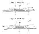
- U.S. Pat. No. 5,894,108 to Mostafazadehdiscloses a typical encapsulated IC package.
- IC package 100illustrated in FIGS. 1A and 1B , is one example of a typical IC package.
- the package 100comprises a die pad 103 , a plurality of leads 101 , and an IC chip 102 mounted to the die pad through an adhesive layer 107 .
- the IC chip 102is electrically joined to the plurality of leads 101 through a plurality of wires 110 .
- the entire packageis protected by an encapsulant 105 , which hardens to protect the elements within and to add support to the package as a whole.
- a IC package according to the present inventionsolves the above-described problem of conventional package encapsulation by providing an enhanced leadframe which permits the encapsulant to become embedded in and locked to the frame.
- a leadframe for an IC packagecomprises an outer frame, a die pad portion disposed within the outer frame, a plurality of lead portions, and a plurality of tie bars connecting the die pad portion to the outer frame.
- the lead portionsextend substantially inward from the outer frame towards the die pad portion.
- At least one of the plurality of lead portionshas a recess formed therein.
- the recesscan comprise a channel formed through each of the lead portions from one side to the opposite side. Alternately, the recess can comprise a dimple-shaped impression.
- At least one of the tie barsalso has a recess formed therein.
- the recesscan comprise a channel or it can comprise a dimple-shaped impression.
- An IC packagecomprises a die pad, having a first face and a second face opposite to the first face, and a plurality of leads, each having a first face and a second face opposite to the first face.
- first and secondare merely used for convenience and do not reflect the order of formation, placement, or observation.
- the leadsare disposed substantially around at least a portion of the die pad.
- the first face of at least one of the leadshas a recess with inner walls formed therein.
- the packagealso comprises an IC chip with a first face and a second face opposite to the first face.
- the second face of the IC chipis coupled to the first face of the die pad.
- the packagealso comprises a plurality of wires linking the IC chip to one of the plurality of leads.
- An encapsulantencloses the IC chip, the plurality of wires, the first face of the die pad, and a portion of the first faces of the leads.
- the encapsulantforms a plurality of side walls. At least one of the side walls intersects the first face of at least one of the leads between the inner walls of the recess formed therein. The encapsulant can fill the recess.
- the recesscan comprise a channel or can comprise a dimple-shaped impression.
- a method of assembling an IC packagecomprises providing a die pad, having a first face and a second face opposite to the first face; a plurality of leads, each having a first face and a second face opposite to the first face; and an IC chip having a first face and a second face opposite to the first face.
- the first face of at least one of the plurality of leadshas a recess with inner walls formed therein.
- the methodalso comprises coupling the second face of the IC chip to the first face of the die pad and electrically connecting the IC chip to the plurality of leads.
- the methodfurther comprises enclosing the IC chip, the first face of the die pad, and a portion of the first face of the plurality of leads with an encapsulant.
- the encapsulantforms a plurality of side walls, at least one of which intersects with the first face of the at least one lead between the inner walls of the recess formed therein.
- the recess formed in the first face of each of the leadscan comprise a channel or can comprise a dimple-shaped impression.
- FIGS. 1A–Bare a cross-sections of a conventional IC package.
- FIGS. 2A–Bare a plane views of leadframes according to an exemplary embodiment of the present invention.
- FIGS. 3A–Care enlarged cross-sections of leads according to exemplary aspects of the present invention.
- FIGS. 4A–Care enlarged plane views of leads according to exemplary aspects of the present invention.
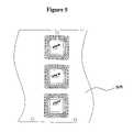
- FIG. 5is a plane view of a leadframe body according to an exemplary aspect of the present invention.
- FIG. 6is a cross-section of an IC package according to an exemplary embodiment of the present invention.
- FIGS. 7A–Eare cross sections illustrating a method of assembling an IC package according to an exemplary embodiment of the present invention.
- FIG. 2Aillustrates a leadframe according a first exemplary embodiment of the present invention.
- the leadframe 200comprises an outer frame 209 , a die pad portion 203 disposed within the outer frame, a plurality of lead portions 201 , and a plurality of tie bars 206 .
- the die pad portion 203can be on the same plane as the outer frame portion 209 , as shown in FIGS. 2A–2B , or it can be vertically offset from the outer frame so that it sits slightly above or slightly below the plane of the outer frame.
- the outer frame, or leadframe bodycan support a single leadframe 200 , as shown in FIGS. 2A–2B , or it can support a number of leadframes, as shown in FIG. 5 .
- FIG. 5illustrates a leadframe body 509 , which supports three leadframes 500 A– 500 C.
- a leadframe body such as illustrated in FIG. 5could also support other numbers of leadframes, as would be understood by one of skill in the art.
- the lead portions 201extend substantially inward from the outer frame 209 towards the die pad portion 203 .
- the tie bars 206connect the die pad portion 203 to the outer frame 209 .
- the tie bars 206support the die pad portion 203 during the manufacture of an IC package, such as the package 600 , illustrated in FIG. 6 .
- At least one of the lead portions 201has a recess 204 A formed therein.
- a majority of the lead portionshave a recess formed therein.
- the recesswhich is formed in the upper face of a lead portion 201 by a mechanical or chemical process can be formed in a number of shapes.
- the recesscan be a channel formed through the upper surface of each of the lead portions 201 from one side to the opposite side thereof, as shown by recess 204 A in FIG. 2A and recess 404 A in FIG. 4A .
- the cross-section of a channel-shaped recesscan be a number of different shapes, as illustrated in FIGS. 3A–3C .
- the channel recesscan have a rectangular cross-section, such as recess 304 A of FIG. 3A .
- itcan have a rounded cross-section, such as recess 304 B of FIG. 3B , or a triangular cross-section, such as recess 304 C of FIG. 3C .
- the cross-section of a channel-shaped recesscan also take any other appropriate shape as would be understood by one of skill in the art.
- the recesscan be in the form of a dimple-shaped impression formed in the upper face of a lead portion 201 , such as illustrated by recess 204 B in FIG. 2B and by recesses 404 B and 404 C of FIGS. 4B–4C .
- a dimple-shaped recessdoes not necessarily reach the sides of the lead portion, as a channel-shaped recess does.
- the cross-section of a dimple-shaped recesscan have a number of different shapes, as illustrated in FIGS. 3A–3C and described above, and as would be understood by one of skill in the art.
- the opening of a dimple-shaped recesscan have a number of different shapes, such as a rounded shape, as illustrated in FIG. 4B , a rectangular shape, as illustrated in FIG. 4C , or any other shape as would be understood by one of skill in the art.
- the purpose of the recess, whether channeln-shaped, dimple-shaped, or otherwise, as would be understood by one of skill in the art,will be explained with reference to an IC package according to a second exemplary embodiment of the present invention.
- recessescan also be formed in the upper surface of at least one of the tie bars 206 of the leadframe 200 .
- FIGS. 2A–2Billustrate such recesses 208 A and 208 B in tie bars 206 .
- the recesses formed in each of the tie barscan be in the form of a channel, or a dimple-shaped impression, or otherwise, as would be understood by one of skill in the art, and can have any of a number of different cross-sections or openings, as would be understood by one of skill in the art.
- the above-mentioned elements of the leadframe 200can be arranged, for example, as illustrated in FIGS. 2A–2B , or according to another arrangement, as would be understood by one of skill in the art.
- the leadframe 200can be composed of a common copper alloy, such as C194, C7025, C151, or Eftec64T, for example.
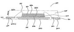
- FIG. 6illustrates an IC package 600 according to a second exemplary embodiment of the present invention.
- the package 600comprises a lead frame, according to the first exemplary embodiment of the present invention, described above.
- the die pad 603 and the leads 601 of FIG. 6correspond to the die pad portion and the lead portions described with respect to the first exemplary embodiment.
- the die pad 603has a first face 603 a and a second face 603 b, opposite to the first face.
- Each of the plurality of leads 601has a first face 601 a and a second face 601 b opposite to the first face. Due to their position in the leadframe, the leads 601 are disposed substantially around at least a portion of the die pad 603 .
- the first face 601 a of at least one of the plurality of leads 601has a recess formed therein.
- the recesscan be in any of a number of forms, as described above with respect to the first exemplary embodiment, and as would be understood by one of skill in the art.
- An adhesive layer 607is disposed on the first face 603 a of the die pad 603 .
- the adhesive layer 607can comprise, for example, electrically conductive or non-conductive epoxy, paste, or adhesive film, or the like, as would be understood by one of skill in the art.
- the package 600also comprises an IC chip 602 , having a first face 602 a and a second face 602 b, opposite to the first face 602 a.
- the second face 602 b of the IC chip 602is coupled to the first face 603 a of the die pad 603 through the adhesive layer 607 .
- a plurality of wires 610electrically conductively join the first face 602 a of the IC chip 602 , and components thereon, to the first face 601 a of each of the plurality of leads 601 .
- the wires 610can be composed of gold, gold, with some level of impurities, aluminum, or copper, for example.
- the goldcan contain 1% impurities, which could include dopants or additives included to improve the properties of the wires, as would be understood by one of skill in the art.
- the IC package 600is enclosed by an encapsulant 605 , which can be composed of a polymer-based molding compound or any other of many known encapsulant materials.
- the encapsulantencloses the IC chip 602 , the plurality of wires 610 , the adhesive layer 607 , the leads 601 , and the die pad 603 , leaving the second faces 601 a and 603 a of the leads 601 and the die pad 603 free from encapsulant.
- the encapsulantforms a substantially planar upper surface 605 a, which is substantially parallel to the first face 602 a of the IC chip 602 .
- the encapsulant 605also forms a plurality of side walls 605 b.
- the side walls 605 bintersect the first faces 601 a of each of the leads 601 within the inner walls of the recesses 604 formed therein.
- the side wallscan slant outward from the upper surface 605 a to the first faces 601 a of each of the leads 601 , as shown in FIG. 6 , or may alternately form straight edges.
- the recesscan be a channel or a dimple-shaped impression formed in the first face of a lead.
- the recesshas a first and a second inner wall.
- recess 304 Ahas a first inner wall 304 A(i) and a second inner wall 304 A(ii).
- the side 305 b of the encapsulant 305intersects with the lead 301 A at a point 350 between the first inner wall 304 A(i) and the second inner wall 304 A(ii).
- the point 350is not necessarily at the mid-point between the two inner walls of the recess 304 A.
- the encapsulant 305fills the recess, as shown.
- the cross-section of the recessmay be rounded, triangular, or of another shape.
- the side walls 305 b of the encapsulant 305will intersect the lead at a point between the inner edges of the recess, as shown in FIGS. 3B and 3C .
- This configuration of the recess and the encapsulantfunctions to lock the encapsulant to the lead, and thereby to the entire encapsulated package. This greatly decreases the chance that the encapsulant, once hardened, will separate from the leads when placed under stress.
- the encapsulantalso serves to provide overall protection to the element is encloses and gives added strength to the package as a whole.
- FIGS. 7A–7Eillustrate a method of assembling an IC package according to a third exemplary embodiment of the present invention.
- a method according to the third exemplary embodiment of the present inventioncomprises providing a die pad 603 having a first face 603 a and a second face 603 b and a plurality of leads 601 , each having a first face 601 a, and a second face 601 b, opposite to the first face 601 a.
- a recess 604having inner walls, is formed in the first face of at least one of the leads 601 .
- the die pad 603 and the plurality of leads 601can be provided for by a leadframe, such as the leadframe 200 , shown in FIGS. 2A–2B , which also comprises a plurality of tie bars and an outer frame (not shown in FIG. 6 ).
- the methodalso comprises coupling the second face 602 b of the IC chip 602 to the first face 603 a of the die pad 603 , and electrically conductively joining the first face 602 a of the IC chip 602 to the first faces 601 a of the plurality of leads 601 .
- the IC chip and the die padcan be coupled through an adhesive layer 607 or by another method as would be understood by one of skill in the art.
- the electric connecting of the IC chip to the leadscan be done with thin wires, such as described above with reference to the second exemplary embodiment.
- the packageis then encapsulated.
- a mold 720is formed around the IC package and an encapsulant 605 can then be injected into the mold, thus surrounding the package.
- the encapsulantremains.
- tie barssuch as those in FIGS. 2A–2B , support the die pad in the proper position.
- the leads 601are supported through their connection to an outer frame, such as shown in FIGS. 2A–2B .
- the encapsulantforms a substantially planar upper surface 605 a, which is substantially parallel to the first face 602 a of the IC chip 602 .
- the encapsulantalso forms a plurality of sides 605 b, at least one of which intersects the first face 601 a of at least one of the leads 601 between the inner walls of the recess formed therein.
Landscapes
- Physics & Mathematics (AREA)
- Engineering & Computer Science (AREA)
- Condensed Matter Physics & Semiconductors (AREA)
- General Physics & Mathematics (AREA)
- Computer Hardware Design (AREA)
- Microelectronics & Electronic Packaging (AREA)
- Power Engineering (AREA)
- Manufacturing & Machinery (AREA)
- Geometry (AREA)
- Lead Frames For Integrated Circuits (AREA)
Abstract
Description
Claims (6)
Priority Applications (1)
| Application Number | Priority Date | Filing Date | Title |
|---|---|---|---|
| US10/812,058US7109570B2 (en) | 2003-09-08 | 2004-03-30 | Integrated circuit package with leadframe enhancement and method of manufacturing the same |
Applications Claiming Priority (2)
| Application Number | Priority Date | Filing Date | Title |
|---|---|---|---|
| US50069603P | 2003-09-08 | 2003-09-08 | |
| US10/812,058US7109570B2 (en) | 2003-09-08 | 2004-03-30 | Integrated circuit package with leadframe enhancement and method of manufacturing the same |
Publications (2)
| Publication Number | Publication Date |
|---|---|
| US20050051876A1 US20050051876A1 (en) | 2005-03-10 |
| US7109570B2true US7109570B2 (en) | 2006-09-19 |
Family
ID=34228749
Family Applications (1)
| Application Number | Title | Priority Date | Filing Date |
|---|---|---|---|
| US10/812,058Expired - LifetimeUS7109570B2 (en) | 2003-09-08 | 2004-03-30 | Integrated circuit package with leadframe enhancement and method of manufacturing the same |
Country Status (1)
| Country | Link |
|---|---|
| US (1) | US7109570B2 (en) |
Cited By (5)
| Publication number | Priority date | Publication date | Assignee | Title |
|---|---|---|---|---|
| US20070267731A1 (en)* | 2006-05-17 | 2007-11-22 | Punzalan Jeffrey D | Integrated circuit package system with different mold locking features |
| US20080272475A1 (en)* | 2005-11-01 | 2008-11-06 | Nxp B.V. | Air Cavity Package for a Semiconductor Die and Methods of Forming the Air Cavity Package |
| US20100320579A1 (en)* | 2009-06-22 | 2010-12-23 | Texax Instruments Incorporated | Metallic Leadframes Having Laser-Treated Surfaces for Improved Adhesion to Polymeric Compounds |
| US20130062651A1 (en)* | 2010-03-25 | 2013-03-14 | Koninklijke Philips Electronics N.V. | Carrier for a light emitting device |
| US20130193567A1 (en)* | 2012-01-31 | 2013-08-01 | Shinko Electric Industries Co., Ltd. | Lead frame and method of manufacturing the same, and semiconductor device and method of manufacturing the same |
Families Citing this family (10)
| Publication number | Priority date | Publication date | Assignee | Title |
|---|---|---|---|---|
| JP2005057067A (en)* | 2003-08-05 | 2005-03-03 | Renesas Technology Corp | Semiconductor device and manufacturing method thereof |
| US20060055063A1 (en)* | 2004-09-13 | 2006-03-16 | Boulin David M | Leadframe designs for plastic overmold packages |
| US20080029855A1 (en)* | 2006-08-04 | 2008-02-07 | Yi-Ling Chang | Lead Frame and Fabrication Method thereof |
| US20080067639A1 (en)* | 2006-09-15 | 2008-03-20 | Stats Chippac Ltd. | Integrated circuit package system with encapsulation lock |
| US8067271B2 (en)* | 2006-09-15 | 2011-11-29 | Stats Chippac Ltd. | Integrated circuit package system with encapsulation lock |
| US8093693B2 (en) | 2006-09-15 | 2012-01-10 | Stats Chippac Ltd. | Integrated circuit package system with encapsulation lock |
| CN102522375B (en)* | 2008-07-30 | 2015-04-08 | 三洋电机株式会社 | Semiconductor device, method for manufacturing semiconductor device, and lead frame |
| TWI421982B (en)* | 2008-11-21 | 2014-01-01 | Advanpack Solutions Pte Ltd | Semiconductor substrate and manufacturing method thereof |
| US9899349B2 (en)* | 2009-01-29 | 2018-02-20 | Semiconductor Components Industries, Llc | Semiconductor packages and related methods |
| CN106129035B (en)* | 2015-05-05 | 2021-01-29 | 恩智浦美国有限公司 | Exposed-pad integrated circuit package with mold lock |
Citations (2)
| Publication number | Priority date | Publication date | Assignee | Title |
|---|---|---|---|---|
| US6197615B1 (en)* | 1997-04-04 | 2001-03-06 | Samsung Electronics Co., Ltd. | Method of producing lead frame having uneven surfaces |
| US6841854B2 (en)* | 2002-04-01 | 2005-01-11 | Matsushita Electric Industrial Co., Ltd. | Semiconductor device |
- 2004
- 2004-03-30USUS10/812,058patent/US7109570B2/ennot_activeExpired - Lifetime
Patent Citations (2)
| Publication number | Priority date | Publication date | Assignee | Title |
|---|---|---|---|---|
| US6197615B1 (en)* | 1997-04-04 | 2001-03-06 | Samsung Electronics Co., Ltd. | Method of producing lead frame having uneven surfaces |
| US6841854B2 (en)* | 2002-04-01 | 2005-01-11 | Matsushita Electric Industrial Co., Ltd. | Semiconductor device |
Cited By (12)
| Publication number | Priority date | Publication date | Assignee | Title |
|---|---|---|---|---|
| US20080272475A1 (en)* | 2005-11-01 | 2008-11-06 | Nxp B.V. | Air Cavity Package for a Semiconductor Die and Methods of Forming the Air Cavity Package |
| US7944062B2 (en)* | 2005-11-01 | 2011-05-17 | Nxp B.V. | Air cavity package for a semiconductor die and methods of forming the air cavity package |
| US20070267731A1 (en)* | 2006-05-17 | 2007-11-22 | Punzalan Jeffrey D | Integrated circuit package system with different mold locking features |
| US8039947B2 (en)* | 2006-05-17 | 2011-10-18 | Stats Chippac Ltd. | Integrated circuit package system with different mold locking features |
| US20100320579A1 (en)* | 2009-06-22 | 2010-12-23 | Texax Instruments Incorporated | Metallic Leadframes Having Laser-Treated Surfaces for Improved Adhesion to Polymeric Compounds |
| US8044495B2 (en)* | 2009-06-22 | 2011-10-25 | Texas Instruments Incorporated | Metallic leadframes having laser-treated surfaces for improved adhesion to polymeric compounds |
| US20120009739A1 (en)* | 2009-06-22 | 2012-01-12 | Texas Instruments Incorporated | Metallic Leadframes Having Laser-Treated Surfaces for Improved Adhesion to Polymeric Compounds |
| US8158460B2 (en)* | 2009-06-22 | 2012-04-17 | Texas Instruments Incorporated | Method of forming metallic leadframes having laser-treated surfaces for improved adhesion to polymeric compounds |
| US20130062651A1 (en)* | 2010-03-25 | 2013-03-14 | Koninklijke Philips Electronics N.V. | Carrier for a light emitting device |
| US8987771B2 (en)* | 2010-03-25 | 2015-03-24 | Koninklijke Philips N.V. | Carrier for a light emitting device |
| US20130193567A1 (en)* | 2012-01-31 | 2013-08-01 | Shinko Electric Industries Co., Ltd. | Lead frame and method of manufacturing the same, and semiconductor device and method of manufacturing the same |
| US8778739B2 (en)* | 2012-01-31 | 2014-07-15 | Shinko Electric Industries Co., Ltd. | Lead frame and method of manufacturing the same, and semiconductor device and method of manufacturing the same |
Also Published As
| Publication number | Publication date |
|---|---|
| US20050051876A1 (en) | 2005-03-10 |
Similar Documents
| Publication | Publication Date | Title |
|---|---|---|
| CN211238167U (en) | Semiconductor device with a plurality of transistors | |
| US7816186B2 (en) | Method for making QFN package with power and ground rings | |
| US6433421B2 (en) | Semiconductor device | |
| US6537856B2 (en) | Method of attaching a semiconductor chip to a leadframe with a footprint of about the same size as the chip and packages formed thereby | |
| US7115441B2 (en) | Semiconductor package with semiconductor chips stacked therein and method of making the package | |
| US8836101B2 (en) | Multi-chip semiconductor packages and assembly thereof | |
| KR100304959B1 (en) | Chip stacked semiconductor package and manufacturing method thereof | |
| US5527743A (en) | Method for encapsulating an integrated circuit package | |
| US7109570B2 (en) | Integrated circuit package with leadframe enhancement and method of manufacturing the same | |
| US6762079B2 (en) | Methods for fabricating dual loc semiconductor die assembly employing floating lead finger structure | |
| US7432128B2 (en) | Method of making semiconductor device | |
| US6946323B1 (en) | Semiconductor package having one or more die stacked on a prepackaged device and method therefor | |
| US7476569B2 (en) | Leadframe enhancement and method of producing a multi-row semiconductor package | |
| US20080164588A1 (en) | High power semiconductor package | |
| US7642638B2 (en) | Inverted lead frame in substrate | |
| US20040124508A1 (en) | High performance chip scale leadframe package and method of manufacturing the package | |
| US20040104457A1 (en) | High density chip scale leadframe package and method of manufacturing the package | |
| US20040217450A1 (en) | Leadframe-based non-leaded semiconductor package and method of fabricating the same | |
| TW201828431A (en) | A Stack Frame for Electrical Connections and the Method to Fabricate Thereof | |
| EP1856738A1 (en) | An integrated circuit device package with an additional contact pad, a lead frame and an electronic device | |
| KR100366111B1 (en) | Structure of Resin Sealed Semiconductor Device | |
| US6838752B2 (en) | Semiconductor package with recessed leadframe and a recessed leadframe | |
| US7001799B1 (en) | Method of making a leadframe for semiconductor devices | |
| US11302569B2 (en) | Method for manufacturing semiconductor device and semiconductor device | |
| KR19990034731A (en) | Lead-on chip lead frames and packages using them |
Legal Events
| Date | Code | Title | Description |
|---|---|---|---|
| AS | Assignment | Owner name:UNITED TEST AND ASSEMBLY TEST CENTER, LTD., SINGAP Free format text:ASSIGNMENT OF ASSIGNORS INTEREST;ASSIGNORS:MANALAC, RODEL;TAN, HIEN BOON;POH, FRANCIS;AND OTHERS;REEL/FRAME:015158/0691 Effective date:20040219 | |
| STCF | Information on status: patent grant | Free format text:PATENTED CASE | |
| AS | Assignment | Owner name:JPMORGAN CHASE BANK, N.A., TEXAS Free format text:SECURITY AGREEMENT;ASSIGNOR:UNITED TEST AND ASSEMBLY CENTER LTD.;REEL/FRAME:020072/0018 Effective date:20071030 Owner name:JPMORGAN CHASE BANK, N.A.,TEXAS Free format text:SECURITY AGREEMENT;ASSIGNOR:UNITED TEST AND ASSEMBLY CENTER LTD.;REEL/FRAME:020072/0018 Effective date:20071030 | |
| AS | Assignment | Owner name:JPMORGAN CHASE BANK, N.A., TEXAS Free format text:SECURITY AGREEMENT;ASSIGNOR:UNITED TEST AND ASSEMBLY CENTER LTD.;REEL/FRAME:020866/0116 Effective date:20080425 Owner name:JPMORGAN CHASE BANK, N.A.,TEXAS Free format text:SECURITY AGREEMENT;ASSIGNOR:UNITED TEST AND ASSEMBLY CENTER LTD.;REEL/FRAME:020866/0116 Effective date:20080425 | |
| FEPP | Fee payment procedure | Free format text:PAYOR NUMBER ASSIGNED (ORIGINAL EVENT CODE: ASPN); ENTITY STATUS OF PATENT OWNER: LARGE ENTITY | |
| FPAY | Fee payment | Year of fee payment:4 | |
| FPAY | Fee payment | Year of fee payment:8 | |
| AS | Assignment | Owner name:UTAC HEADQUARTERS PTE. LTD., SINGAPORE Free format text:ASSIGNMENT OF ASSIGNORS INTEREST;ASSIGNOR:UNITED TEST AND ASSEMBLY CENTER LIMITED;REEL/FRAME:037959/0822 Effective date:20150508 | |
| AS | Assignment | Owner name:UTAC HEADQUARTERS PTE. LTD., SINGAPORE Free format text:CORRECTIVE ASSIGNMENT TO CORRECT THE TO ADD THE ANNEX A AND THE ANNEX B WHICH WAS INADVERTENTLY LEFTOUT IN THE ORIGINAL ASSIGNMENT DOCUMENT PREVIOUSLY RECORDED ON REEL 037959 FRAME 0822. ASSIGNOR(S) HEREBY CONFIRMS THE ASSIGNMENT;ASSIGNOR:UNITED TEST AND ASSEMBLY CENTER LIMITED;REEL/FRAME:039885/0541 Effective date:20150508 | |
| AS | Assignment | Owner name:UTAC HEADQUARTERS PTE. LTD., SINGAPORE Free format text:CORRECTIVE ASSIGNMENT TO CORRECT THE INCLUDE PATENT NUMBER 8816482 PREVIOUSLY RECORDED AT REEL: 039885 FRAME: 0541. ASSIGNOR(S) HEREBY CONFIRMS THE ASSIGNMENT;ASSIGNOR:UNITED TEST AND ASSEMBLY CENTER LIMITED;REEL/FRAME:043979/0820 Effective date:20150508 | |
| AS | Assignment | Owner name:UNITED TEST AND ASSEMBLY CENTER LTD., SINGAPORE Free format text:RELEASE BY SECURED PARTY;ASSIGNOR:JPMORGAN CHASE BANK, N.A.;REEL/FRAME:044549/0152 Effective date:20130207 | |
| MAFP | Maintenance fee payment | Free format text:PAYMENT OF MAINTENANCE FEE, 12TH YEAR, LARGE ENTITY (ORIGINAL EVENT CODE: M1553) Year of fee payment:12 |