US7109544B2 - Architecture for vertical transistor cells and transistor-controlled memory cells - Google Patents
Architecture for vertical transistor cells and transistor-controlled memory cellsDownload PDFInfo
- Publication number
- US7109544B2 US7109544B2US10/777,128US77712804AUS7109544B2US 7109544 B2US7109544 B2US 7109544B2US 77712804 AUS77712804 AUS 77712804AUS 7109544 B2US7109544 B2US 7109544B2
- Authority
- US
- United States
- Prior art keywords
- transistor
- active
- regions
- trenches
- region
- Prior art date
- Legal status (The legal status is an assumption and is not a legal conclusion. Google has not performed a legal analysis and makes no representation as to the accuracy of the status listed.)
- Expired - Fee Related, expires
Links
- 230000015654memoryEffects0.000titleclaimsabstractdescription38
- 239000003990capacitorSubstances0.000claimsabstractdescription30
- 239000000758substrateSubstances0.000claimsabstractdescription28
- 238000003860storageMethods0.000claimsabstractdescription25
- 239000002800charge carrierSubstances0.000claimsabstractdescription13
- 238000002955isolationMethods0.000claimsdescription80
- 239000012212insulatorSubstances0.000claimsdescription15
- 239000000463materialSubstances0.000claimsdescription11
- 239000010410layerSubstances0.000claims13
- 239000002356single layerSubstances0.000claims2
- 238000009825accumulationMethods0.000abstractdescription4
- 230000000694effectsEffects0.000abstractdescription4
- 239000002243precursorSubstances0.000description29
- 238000000034methodMethods0.000description27
- 239000004065semiconductorSubstances0.000description23
- 238000004519manufacturing processMethods0.000description17
- 238000002513implantationMethods0.000description10
- 230000015572biosynthetic processEffects0.000description9
- 238000000151depositionMethods0.000description5
- 230000008021depositionEffects0.000description5
- 238000005530etchingMethods0.000description5
- 239000004020conductorSubstances0.000description4
- 238000000623plasma-assisted chemical vapour depositionMethods0.000description4
- 230000001419dependent effectEffects0.000description3
- 239000007772electrode materialSubstances0.000description3
- 238000000059patterningMethods0.000description3
- 229910052581Si3N4Inorganic materials0.000description2
- 239000005388borosilicate glassSubstances0.000description2
- 239000000969carrierSubstances0.000description2
- 238000005137deposition processMethods0.000description2
- 238000005468ion implantationMethods0.000description2
- 239000011253protective coatingSubstances0.000description2
- HQVNEWCFYHHQES-UHFFFAOYSA-Nsilicon nitrideChemical compoundN12[Si]34N5[Si]62N3[Si]51N64HQVNEWCFYHHQES-UHFFFAOYSA-N0.000description2
- VYPSYNLAJGMNEJ-UHFFFAOYSA-NSilicium dioxideChemical compoundO=[Si]=OVYPSYNLAJGMNEJ-UHFFFAOYSA-N0.000description1
- XUIMIQQOPSSXEZ-UHFFFAOYSA-NSiliconChemical compound[Si]XUIMIQQOPSSXEZ-UHFFFAOYSA-N0.000description1
- 230000006978adaptationEffects0.000description1
- HAYXDMNJJFVXCI-UHFFFAOYSA-Narsenic(5+)Chemical compound[As+5]HAYXDMNJJFVXCI-UHFFFAOYSA-N0.000description1
- 230000006399behaviorEffects0.000description1
- 210000000746body regionAnatomy0.000description1
- 239000005380borophosphosilicate glassSubstances0.000description1
- 238000010586diagramMethods0.000description1
- 238000011065in-situ storageMethods0.000description1
- 230000003071parasitic effectEffects0.000description1
- 238000005498polishingMethods0.000description1
- 238000007493shaping processMethods0.000description1
- 229910052710siliconInorganic materials0.000description1
- 239000010703siliconSubstances0.000description1
- 229910052814silicon oxideInorganic materials0.000description1
- 125000006850spacer groupChemical group0.000description1
- 239000000126substanceSubstances0.000description1
- 230000007704transitionEffects0.000description1
Images


Classifications
- H—ELECTRICITY
- H10—SEMICONDUCTOR DEVICES; ELECTRIC SOLID-STATE DEVICES NOT OTHERWISE PROVIDED FOR
- H10B—ELECTRONIC MEMORY DEVICES
- H10B12/00—Dynamic random access memory [DRAM] devices
- H—ELECTRICITY
- H10—SEMICONDUCTOR DEVICES; ELECTRIC SOLID-STATE DEVICES NOT OTHERWISE PROVIDED FOR
- H10B—ELECTRONIC MEMORY DEVICES
- H10B12/00—Dynamic random access memory [DRAM] devices
- H10B12/30—DRAM devices comprising one-transistor - one-capacitor [1T-1C] memory cells
- H10B12/34—DRAM devices comprising one-transistor - one-capacitor [1T-1C] memory cells the transistor being at least partially in a trench in the substrate
- H—ELECTRICITY
- H10—SEMICONDUCTOR DEVICES; ELECTRIC SOLID-STATE DEVICES NOT OTHERWISE PROVIDED FOR
- H10B—ELECTRONIC MEMORY DEVICES
- H10B12/00—Dynamic random access memory [DRAM] devices
- H10B12/01—Manufacture or treatment
- H10B12/02—Manufacture or treatment for one transistor one-capacitor [1T-1C] memory cells
- H10B12/05—Making the transistor
- H10B12/053—Making the transistor the transistor being at least partially in a trench in the substrate
Definitions
- the minimum feature sizemay be reduced in lithography-dictated steps, in which case memory cell concepts can be transferred from a larger minimum feature size to a smaller minimum feature size without additional changes beyond shrinking of the memory cell structures to scale.
- Well-scalable memory cell conceptsare advantageous since an additional outlay for changes in a layout of the memory cell structures over and above adaptations that are purely to scale is limited in the event of a transition to a smaller feature size.
- a known approach to reducing the space requirement of a memory cellis to provide the selection transistor in a structure that is vertical with respect to the transistor plane.
- the source/drain connection regions(S/D junctions) are arranged essentially vertically one above the other relative to the transistor plane.
- a channel controlled by a gate electrode of the selection transistoris then formed, principally in a direction perpendicular to the transistor plane, in an active region of the selection transistor which is provided between the two source/drain connection regions of the selection transistor.
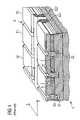
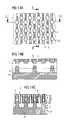
- An architecture having vertical transistor cellsis disclosed for example in U.S. Pat. No. 6,352,894 B1 (Goebel et al.) and illustrated in FIG. 1 , which is adapted from the Figures of the above patent specification.
- FIG. 1shows a plurality of transistor cells 81 arranged on a substrate 1 .
- each transistor cell 81has an upper source/drain connection region 4 and a lower source/drain connection region 2 .
- An active region (also called body region) 3is in each case formed between upper 4 and lower 2 source/drain connection regions.
- transistor cells 81are respectively arranged in rows and columns arranged at right angles to one another, the rows extending along an x direction and the columns extending along a y direction perpendicular to the x direction. Within a row, respectively adjacent transistor cells 81 are separated by narrow isolation trenches 6 . Adjacent rows are isolated from one another by wide active trenches 5 . First sections of gate electrodes 52 are formed in narrow isolation trenches 6 .
- Two mutually insulated word lines 521 , 522 which are respectively assigned to one of the adjacent rowspass through wide active trenches 5 , said word lines forming second sections of gate electrodes 52 .
- Gate electrodes 52 respectively arranged in a roware conductively connected to one another via word lines 521 , 522 .
- Gate electrode 52 of each transistor cell 81surrounds active region 3 from four sides.
- Lower source/drain connection regions 2 of transistor cells 81are formed as sections of a connection plate (buried plate) 21 , which, in an upper region, is patterned by active trenches 5 and isolation trenches 6 , and are electrically conductively connected to one another.
- Gate electrode 52 of a transistor cell 81is insulated from active region 3 of assigned transistor cell 81 by a gate dielectric 51 .
- An insulator layer 50insulates source/drain connection regions 2 , 4 from adjoining conductive structures and is opened section by section for the connection of the upper source/drain connection regions, for instance to an electrode of a storage capacitor, in the course of a further processing.
- a disadvantage of the illustrated architecture of transistor cells 81is that active regions 3 of transistor cells 81 are electrically without connection.
- transistor cell architecture illustrated in FIG. 1it is possible, with a minimum feature size F, to produce memory cells with a planar area requirement of 4 F 2 , or 8 F 2 in the case of memory concepts with a so-called folded bit line structure.
- An additional connection for the active region of each transistor cell according to a conventional typewould considerably increase the area requirement of the transistor cell.
- Embodiments of the present inventionprovide for a transistor cell architecture and memory cell architecture in which a functional restriction of the transistor cells by a floating body effect is reduced without increasing an area requirement significantly, with respect to conventional memory cell concepts for 4 F 2 or 8 F 2 transistor cells or 4 F 2 or 8 F 2 memory cells. Further embodiments include a method for fabricating such a transistor cell or memory cell.
- vertical transistor cellsare arranged in a transistor cell array, in a transistor plane, in a manner that is initially known.
- the transistor cellsare arranged in rows in an x direction, said rows being separated from one another by active trenches, and in columns in a y direction perpendicular to the x direction, said columns being separated by isolation trenches.
- Each transistor cellhas a lower source/drain connection region, an upper source/drain connection region and an active region formed between the lower and the upper source/drain connection region.
- a formation of a conductive channel between the two source/drain connection regionsis controlled in the active region, in the operating state of the transistor cell, in a manner dependent on a potential at a gate electrode which is insulated from the active region by a gate dielectric.
- the active regions at least of transistor cells which are adjacent to one another in the x directionare now connected to one another, enabling a charge carrier transport between the active regions of transistor cells which are adjacent at least in each case in the x direction. Floating body effects are avoided.
- the gate electrodesare arranged in the active trenches.
- the gate electrodes of transistor cells which are adjacent in each case in the x directionare connected to one another and form word lines.
- a method for fabricating vertical transistor cells in a substratecomprises arranging said transistor cells in a transistor cell array in rows along an x direction and in columns along a y direction perpendicular to the x direction and firstly providing a conductive connection plate in the substrate.
- a precursor layer bodyis arranged on the conductive connection plate. Isolation trenches extending along the y direction are introduced into an upper region of the precursor layer body, wherein transistor cells adjacent in the x direction are separated from one another by said isolation trenches.
- active trenches which cut through the precursor layer body and pattern the connection plate in an upper regionare introduced into the precursor layer body.
- layer bodies separated by the active trenchesemerge from the precursor layer body.
- Lower source/drain connection regionsarise from the upper regions of the connection plate. Active regions of the transistor cells which are connected to one another by means of the lower regions of the layer bodies row by row emerge from the upper regions of the layer bodies.
- a method for fabricating vertical transistor cells in a substratecomprises arranging said transistor cells in a transistor cell array, in rows along an x direction and in columns along a y direction perpendicular to the x direction, and firstly providing a conductive connection plate in the substrate. Additionally, the connection plate is then patterned in an upper region in such a way that a lower source/drain connection region which is delimited both in the x direction and in the y direction is produced in the upper region per transistor cell. Furthermore, a contiguous layer body which is patterned by the lower source/drain connection regions in a lower region is arranged on the connection plate, in the upper region of which layer body active regions of the transistor cells are formed.
- the layer bodyis not divided into mutually separated layer bodies respectively assigned to a transistor row, the active regions of transistor cells adjacent in the x direction as well as transistor cells adjacent in the y direction, for example, comprising all the transistor cells of a transistor cell array, can be connected to one another in this way.
- FIG. 1depicts a diagrammatic perspective illustration of a known architecture of transistor cells in a substrate.
- FIG. 2depicts a diagrammatic cross section along an x direction through a transistor cell architecture processed in accordance with a first exemplary embodiment of a method according to the invention in a first production phase.
- FIG. 3depicts a diagrammatic cross section transversely with respect to the x direction through a transistor cell architecture processed in accordance with the first exemplary embodiment in the first production phase.
- FIG. 4depicts a diagrammatic cross section transversely with respect to the x direction through a transistor cell architecture processed in accordance with the first exemplary embodiment in a second production phase.
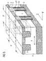
- FIG. 5depicts a diagrammatic perspective illustration of a transistor cell architecture processed in accordance with the first exemplary embodiment in a third production phase.
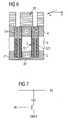
- FIG. 6depicts a diagrammatic cross section transversely with respect to the x direction through a memory cell architecture processed in accordance with the first exemplary embodiment in a fourth production phase.
- FIG. 7depicts a diagrammatic circuit diagram of a memory cell.
- FIG. 8depicts a diagrammatic cross section transversely with respect to the x direction through a transistor cell architecture processed in accordance with a second exemplary embodiment in a first production phase.
- FIG. 9depicts a diagrammatic cross section transversely with respect to the x direction through a transistor cell architecture processed in accordance with the second exemplary embodiment in a second production phase.
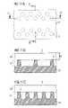
- FIG. 10A and 10Bdepict a simplified plan view and a diagrammatic cross section transversely with respect to the x direction of a transistor cell architecture processed in accordance with a third exemplary embodiment in a first production phase.
- FIGS. 11A , 11 B, and 11 Cdepict a simplified plan view, diagrammatic cross sections along an x direction, and transverse to the x direction of a transistor cell architecture, respectively, processed in accordance with the third exemplary embodiment in a further production step.
- FIGS. 12A , 12 B, and 12 Cdepict a simplified plan view, diagrammatic cross sections along an x direction, and transverse to the x direction of a transistor cell architecture, respectively, processed in accordance with the third exemplary embodiment in a further production step.
- FIGS. 13A , 13 B, and 13 Cdepict a simplified plan view, diagrammatic cross sections along an x direction, and transverse to the x direction of a transistor cell architecture, respectively, processed in accordance with the third exemplary embodiment in a further production step.
- FIGS. 14A , 14 B, and 14 Cdepict a simplified plan view, diagrammatic cross sections along an x direction, and transverse to the x direction of a transistor cell architecture, respectively, processed in accordance with the third exemplary embodiment in a further production step.
- FIGS. 15A , 15 B, and 15 Cdepict a simplified plan view, diagrammatic cross sections along an x direction, and transverse to the x direction of a transistor cell architecture, respectively, processed in accordance with the third exemplary embodiment in a further production step.
- FIGS. 16A , 16 B, and 16 Cdepict a simplified plan view, diagrammatic cross sections along an x direction, and a cross section transverse to the x direction, respectively of a transistor cell architecture processed in accordance with a fourth exemplary embodiment at a certain process step.
- FIGS. 17A , 17 B, and 17 Cdepict a simplified plan view, diagrammatic cross sections along an x direction, and a cross section transverse to the x direction, respectively a transistor cell architecture processed in accordance with a fourth exemplary embodiment at a later process step.
- FIGS. 2 to 7illustrate the fabrication of a transistor cell architecture according to a first exemplary embodiment of the present invention at various steps, using cross sections and a perspective illustration of the transistor cell architecture
- a weakly p-doped epitaxial layerwhich forms a precursor layer body 3 ′′, is provided by in-situ doping of a silicon layer deposed on a connection plate 21 , the latter formed as an n-doped layer in a substrate 1 .
- a working layer 91typically made of silicon nitride, is deposited on the precursor layer body 3 ′′.
- Shallow isolation trenches 6are formed in a first lithographic step. Isolation trenches 6 extend parallel to one another along a y direction. The depth of shallow isolation trenches 6 is dimensioned such that the shallow isolation trenches 6 do not reach connection plate 21 and end in the region of precursor layer body 3 ′′.
- Precursor layer body 3 ′′is thus preserved in a contiguous fashion in a lower region after the formation of shallow isolation trenches 6 .
- precursor layer body 3 ′′is patterned by isolation trenches 6 .
- Isolation trenches 6are filled with a dielectric, typically silicon oxide.
- FIG. 2The state of the processed transistor cell architecture after isolation trenches 6 have been filled with a dielectric is illustrated in simplified fashion in FIG. 2 , which displays a cross section along an x direction perpendicular to the y direction.
- FIG. 3illustrates a cross section perpendicular to the x direction after a subsequent formation of deep active trenches 5 .
- a mask 92typically a borosilicate glass (BSG)
- BSGborosilicate glass
- Active trenches 5extend into the connection plate 21 and pattern connection plate 21 in an upper region.
- lower source/drain connection regions 2emerge from the upper sections of connection plate 21
- layer bodies 3 ′ separated from one another by active trenches 5emerge from precursor layer body 3 ′′ of FIG. 2 .
- Each layer body 3 ′forms an active region 3 of a transistor cell between in each case two isolation trenches 6 which are adjacent within a row.
- a gate dielectric 51is deposited or produced at the inner walls of active trenches 5 .
- Two mutually insulated word lines 521 , 522are then produced in a known manner, for instance by means of a conformal deposition of a conductive material and a subsequent isotropic etching of the deposited material at the inner walls of active trenches 5 .
- Word lines 521 , 522extend in the x direction along active trenches 5 . Between two respectively adjacent shallow isolation trenches 6 , two sections of word lines 521 , 522 which are respectively opposite each other at an active region 3 form gate electrodes of a transistor cell.
- FIG. 4depicts the state of the transistor cell architecture after the formation of word lines 521 , 522 and the removal of mask 92 .
- active trenches 5are filled with a word line insulator (inter wordline fill) 53 .
- CMPchemical mechanical polishing step
- transistor cells 81The resulting architecture of transistor cells 81 is shown in simplified fashion in a perspective illustration in FIG. 5 . If a transistor cell 81 is fabricated according to a lithography-determined minimum feature size F, then an area requirement of 4 F 2 results for transistor cell 81 , as can be observed directly from FIG. 5 .
- Lower source/drain connection regions 2 of transistor cells 81are sections of contiguous connection plate 21 which is patterned in an upper region. Active regions 3 of transistor cells 81 which are adjacent in the x direction are connected to one another, since the shallow isolation trenches 6 do not extend as far as connection plate 21 , so that charge carriers which otherwise accumulate in the active regions 3 can flow away in layer body 3 ′ along the x direction.
- contiguous active regions 3 which run parallelmay be connected in a suitable manner, thereby ensuring that charge carriers are continuously transported away from active regions 3 and avoiding a disadvantageous accumulation of charge carriers in active regions 3 .
- a memory cellcomprises a transistor cell 81 and a storage capacitor 82 .
- Transistor cell 81is connected to an electrode of storage capacitor 82 via upper source/drain connection region 4 .
- transistor cells 81proceeds from an n-doped layer of a substrate 1 , which layer is provided as a common electrical connection of the transistor cells arranged to form a transistor cell array (common plate line) and forms a connection plate 21 .
- a layer which is initially undoped or only weakly p-dopedis arranged above n-doped connection plate 21 , from which layer active regions 3 and lower source/drain connection regions 2 of transistor cells 81 emerge in the course of fabrication.
- the undoped (or weakly p-doped) layerforms a precursor layer body 3 ′′, either produced by means of an epitaxial method or from a monocrystalline semiconductor material of substrate 1 .
- firstly active trenches 5are formed along an x direction and isolation trenches of essentially the same depth are formed in a y direction perpendicular to the x direction.
- active trenches 5 and the isolation trenchesend within precursor layer body 3 ′′ and do not reach connection plate 21 .
- Active trenches 5 extending along the x directionare provided with a larger width, for example, more than double the width of the isolation trenches extending along the y direction.
- Precursor layer body 3 ′′initially remains unpatterned in a lower region below trenches 5 , 6 .
- semiconductor webs isolated from one another by trenches 5 , 6are formed in precursor layer body 3 ′′, which webs have a longitudinal extent of, for example, twice the minimum feature size F in the x direction and a transverse extent of about 0.8 F in the y direction.
- the width of the active trenchesis 2 F and the width of the isolation trenches is 0.8 F.
- a process layer 71is deposited, for instance by means of plasma enhanced chemical vapor deposition (PECVD), onto precursor layer body 3 ′′ patterned by trenches 5 , 6 .
- the material of process layer 71typically silicon nitride, is provided with a larger thickness on the semiconductor webs than at the bottom of active trenches 5 .
- the narrow isolation trenchesare essentially covered by process layer 71 growing on the semiconductor webs while wide active trenches 5 are not completely covered.
- process layer 71is deposited in such a way that it protrudes from the semiconductor webs to an extent in each case of at least 0.4 F, but preferably 0.6 F, over adjacent isolation trenches 6 and active trenches 5 .
- isolation trenches 6 having a width of 0.8 Fare reliably overgrown, while active trenches 5 having a width of 2 F remain open.
- portions of process layer 71are removed from the bottom region of wide active trenches 5 in a subsequent etching step, while the bottom region of the narrow isolation trenches remains covered by process layer 71 which has grown together above the semiconductor webs over the isolation trenches.
- lower source/drain connection regions 2are formed in sections of precursor layer body 3 ′′ located below active trenches 5 , said source/drain connection regions in each case adjoining connection plate 21 .
- the source drain regionsare formed using arsenic ion implantation at about 100 to 200 keV, for gate structures of 70 nm.
- a gate dielectric(not shown) is produced at least in sections at the walls of active trenches 5 , optionally also at the walls of isolation trenches 6 .
- a conductive materialis then deposited conformally, preferably with a thickness of 0.6 F, for example, for the exemplary embodiment, in order to form the gate electrodes.
- the conductive materialis caused to recede by means of an isotropic etching step to an extent such that the conductive material remains along vertical side areas of the semiconductor webs (spacer etch).
- the narrow isolation trenches which isolate transistor cells 81 from one another in the x directionare filled by the gate electrode material at least to an extent such that gate electrodes 52 of transistor cells 81 which are adjacent in the x direction adjoin one another and word lines 521 extending along the x direction are formed.
- gate electrodes 52 or word lines 521do not completely cover the side areas of the semiconductor webs, but rather extend from a height of the semiconductor webs which is determined by the deposition process for the gate electrode material and the subsequent etching step as far as the bottom of trenches 5 , 6 .
- the upper region of the semiconductor web which is not enclosed by gate electrodes 521can thereby subsequently be formed, by means of an inclined implantation, as a respective upper source/drain connection region 4 of the respective transistor cell 81 .
- the inclined implantationis effected in a self-aligned manner with respect to gate electrodes 52 or with respect to word lines 521 .
- an active region 3is formed for each transistor cell 81 between two isolation trenches 6 which are adjacent in the x direction (see FIG. 5 ) and between lower and upper source/drain connection regions 2 , 4 .
- the state of the transistor cell architecture illustrated diagrammatically in FIG. 9results after active trenches 5 have been filled with a word line insulator (inter wordline fill) and removal of excess material deposited above an upper edge of upper source/drain connection regions 4 .
- a storage capacitoris subsequently arranged on upper source/drain connection region 4 in a known manner.
- FIGS. 10 to 15illustrate various steps of a method applicable to both transistor cell architecture and memory cell fabrication according to an exemplary embodiment of the present invention.
- a transistor cellis produced with a gate structure in which two sections of a gate electrode are formed at two opposite side areas of an active region (double gate transistor, or DGT).
- connection plate 21common plate line, buried layer
- a first epitaxial layer 31is provided on connection plate 21 , in which layer lower source/drain connection regions 2 are formed in the course of a first lithographic step and a masked implantation.
- lower source/drain connection regions 2each adjoin connection plate 21 and are formed for instance as conical or cylindrical vertical structures which project through first epitaxial layer 31 in insular fashion.
- the non-doped sections of first epitaxial layer 31form a contiguous first section of a layer body 3 ′.
- FIG. 10Aillustrates first epitaxial layer 31 with lower source/drain connection regions 2 and the contiguous first section of layer body 3 ′ in plan view.
- FIG. 10Bdepicts a cross section through first epitaxial layer 31 arranged on connection plate 21 , in which layer lower source/drain connection regions 2 and the first section of layer body 3 ′ are formed in sections.
- a second epitaxial layer 32is then grown, the thickness of which defines a channel length KL of the transistor cells to be produced.
- FIG. 11Ashows a plan view of lower source/drain connection regions 2 covered by second epitaxial layer 32 .
- FIGS. 11B and 11Cshow cross sections through second epitaxial layer 32 arranged on first epitaxial layer 31 and layer body 3 ′ encompassing second epitaxial layer 32 and the sections of first epitaxial layer 31 which are not formed as lower source/drain connection regions 2 .
- FIGS. 12A–Cillustrate the state of the resulting transistor cell architecture after introduction of active trenches 5 performed in a subsequent step.
- FIGS. 12A–Creveal the architecture of active trenches 5 and additionally that of semiconductor webs 33 relative to lower source/drain connection regions 2 .
- Lower source/drain connection regions 2which are adjacent in each case in the x direction, are partially made free by two active trenches 5 which are adjacent in the y direction perpendicular to the x direction.
- FIG. 12Billustrates a cross section through the architecture along the x direction.
- the depth ATD of active trenches 5is greater than the channel length KL. lower source/drain connection regions 2 thus project into semiconductor webs 33 .
- FIG. 12Cshows a cross section through the architecture of FIG. 12 perpendicular to the x direction.
- a gate dielectric 51is then formed at the side walls of semiconductor webs 33 , for instance by growth or deposition of an oxide.
- two mutually insulated gate electrodes 52 or word lines 521are formed at the mutually opposite longitudinal sides of active trenches 5 in a known manner.
- the gate electrodesare formed by conformal deposition of a gate electrode material and a subsequent isotropic etching-back.
- sections of word lines 521which extend along the x direction along active trenches 5 respectively act as gate electrodes 52 of respectively assigned transistor cell 81 .
- Active trenches 5are then filled with a word line insulator (inter wordline fill) 53 .
- firstly word line insulator 53 and gate electrodes 52are etched back.
- upper sections of semiconductor webs 33are n-doped, thus forming a preliminary stage 4 ′ of upper source/drain connection regions 4 of transistor cells 81 .
- active trenches 5are filled completely with the word line insulator.
- FIG. 13Cillustrates active trenches 5 in cross section.
- active trenches 5are lined with a gate dielectric 51 .
- a word line 521is respectively formed at the side walls of active trenches 5 .
- the trenchesare completely filled with a word line insulator 53 .
- Preliminary stages 4 ′ of upper source/drain connection regions 4have been formed in the upper region of semiconductor webs 33 of FIG. 12C .
- FIG. 13Bfurthermore reveals that active regions 3 of transistor cells 81 that are adjacent in each case in the x direction and the y direction are sections of a layer body 3 ′, which is contiguous in the lower region and are therefore connected to one another.
- FIGS. 14A–Creveal one possibility for the patterning of upper source/drain connection regions 4 according to an exemplary embodiment of the present invention.
- the patterningis done by the introduction of isolation trenches 6 into preliminary stage 4 ′ of the upper source/drain connection regions, resulting in the emergence of upper source/drain connection regions 4 .
- isolation trenches 6are provided with a depth which is greater than the extent of upper source/drain connection regions 4 into the depth of the substrate.
- the arrangement of the isolation trenches 6may be produced to correspond to the architecture of lower source/drain connection regions 2 , and in a manner dependent on an arrangement of storage capacitors 82 formed in a subsequent step as illustrated in FIGS. 15A–C .
- first isolation trenches 6are in each case arranged above lower source/drain connection regions 2 .
- an additional isolation trench 6is in each case provided between two first isolation trenches 6 .
- Isolation trenches 6are introduced either non-material-selectively in accordance with FIG. 14A or, in accordance with FIG. 14C , selectively with respect to the filling material of active trenches 5 in the semiconductor material of upper source/drain connection regions 4 or layer body 3 ′.
- FIGS. 15A–Cillustrate one possibility for the positioning of storage capacitors: in plan view in FIG. 15A and in two mutually orthogonal cross sections in FIG. 15B and FIG. 15C .
- the storage capacitorsare formed as stacked capacitors according to a known type.
- the memory cell illustrated in FIGS. 15A–Ccomprises a storage capacitor 82 and a transistor cell 81 .
- Transistor cell 81has a lower source/drain connection region 2 and an upper source/drain connection region 4 , which delimit an active region 3 in each case in the vertical direction.
- Lower source/drain connection region 2imparts a connection to a common connection structure of transistor cells 81 , connection plate 21 .
- Upper source/drain connection region 4imparts an electrical connection to storage capacitor 82 .
- Lying opposite active region 3 of a transistor cell 81are gate electrodes 52 on a gate dielectric 51 in active trenches 5 . An electrical potential at gate electrodes 52 controls the formation of a conductive channel in active region 3 .
- Gate electrodes 52 of transistor cells 81which are adjacent along active trenches 5 , are formed in sections by continuous word lines 521 . Word lines 521 respectively opposite an active region 3 are driven jointly.
- Transistor cells 81which are adjacent in the longitudinal direction of active trenches 5 , are separated from one another by isolation trenches 6 . Active regions 3 of all transistor cells 81 are sections of a contiguous layer body 3 ′.
- FIGS. 16 A–C and 17 A–Cillustrate important steps of a method for fabricating a transistor cell architecture according to an exemplary embodiment of the present invention.
- a transistor cell with a gate structureis produced where the gate electrodes essentially completely surround an active region of the transistor cell (surrounding gate transistor, or SGT).
- the initial processing up to and including the formation of active trenches 5corresponds to steps illustrated in FIG. 10 to FIG. 12 .
- a protective coating(not illustrated) is then deposited onto the surface of layer body 3 ′ patterned by active trenches 5 , followed by the deposition of a mask 92 , comprising, for instance, borophosphosilicate glass.
- active trenches 5are temporarily filled with the mask material.
- mask 92is patterned in accordance with the desired architecture of isolation trenches 6 , followed by introduction of isolation trenches 6 into layer body 3 ′ by means of an etching process using mask 92 .
- FIG. 16Ashows the resulting architecture after the introduction of isolation trenches 6 into layer body 3 ′ in plan view, with mask 92 omitted.
- the architecture of isolation trenches 6 relative to lower source/drain connection regions 2is produced in a manner corresponding to the architecture of lower source/drain connection regions 2 , and is dependent, for instance, on an architecture of storage capacitors formed subsequently.
- first isolation trenches 6are in each case provided above lower source/drain connection regions 2 .
- an additional isolation trench 6is in each case provided between two first isolation trenches 6 .
- FIG. 16Breveals that isolation trenches 6 are in this case provided with a depth which is greater than the extent of upper source/drain connection regions 4 yet to be formed ( FIG. 17 ).
- FIG. 16Creveals that isolation trenches 6 are introduced selectively into the semiconductor material of layer body 3 ′.
- isolation trenches 6After the shaping of isolation trenches 6 , residual sections of mask 92 and also the protective coating are removed. As depicted in FIG. 17 , both in active trenches 5 and in isolation trenches 6 a gate dielectric 51 , gate electrodes 52 , and also a word line insulator 53 , are provided, and upper source/drain connection regions 4 are formed from upper sections of layer body 3 ′.
- FIG. 17Ashows a plan view of the architecture after portions of word line insulator 53 , formed temporarily above the upper edge of upper source/drain connection regions 4 , have been caused to recede. The uncovered upper source/drain connection regions 4 are embedded in word line insulator 53 .
- FIGS. 17B and 17Cfurthermore reveal that active regions 3 formed in layer body 3 ′ and respectively assigned to a transistor cell, are in each case enclosed from four sides by gate electrodes arranged in active trenches 5 and isolation trenches 6 . Finally, it furthermore emerges from FIG. 17 that active regions 3 of the transistor cells of a transistor cell array are in each case sections of contiguous layer body 3 ′.
- exemplary embodiments of the present inventionprovide an architecture for transistor and memory cells arranged in a vertical fashion.
- the connection between the active regions of adjacent transistor cellscan be realized in different ways.
- the active regionsare sections of one or a plurality of layer bodies.
- the layer bodyis patterned by the active trenches and the isolation trenches in an upper region.
- a layer bodyconnects the active regions of transistor cells which are adjacent to one another at least in the x direction.
- the layer bodiesare preferably lengthened row by row into a connection array adjoining the transistor cell array.
- the layer bodiesare connected to one another, thereby also enabling a charge carrier transport between transistor cells which are adjacent in the y direction.
- the layer bodiesare individually or jointly connected to a structure whose potential is controlled in the operating state of the transistor cell such that an accumulation of charge carriers in the active regions or the layer body or bodies is avoided.
- the potentialis the potential of a carrier substrate (bulk).
- the lower source/drain connection regions of the transistor cellsare in each case connected to a contiguous connection plate or are particularly preferably in each case sections of a connection plate which is patterned at least in an upper region and is contiguous in a lower region.
- an architecturecomprises a connection plate patterned in an upper region by the active trenches extending along the x direction.
- lower source/drain connection regions extending along the x directionare formed in the upper region of the connection plate.
- the isolation trenches running along the y directionhave a smaller depth than the active trenches. Therefore, the layer bodies are formed contiguously row by row in each case in a lower region below the isolation trenches.
- the gate electrodesmay be arranged in the isolation trenches.
- the isolation trenchesare preferably filled with an insulator material. This results in a significantly simplified process flow for the fabrication of the transistor architecture.
- an architecturecomprises isolation trenches and active trenches that have an essentially identical depth.
- the connection plateagain has, in an upper region, lower source/drain connection regions extending along the x axis, the source/drain connection regions essentially being arranged below the active trenches in the case of this embodiment.
- the layer bodiesare formed contiguously row by row in each case below the active regions and are separated from one another by the lower source/drain connection regions and the active trenches.
- the architectureenables the connection of the active regions in the context of the boundary conditions which are necessary for a minimum area requirement of the transistor cell.
- the active regions of the transistor cellspreferably have a cross-sectional area of essentially 1 F 2 relative to a production-dictated minimum feature size F parallel to the transistor plane.
- the area requirement of a transistor cellis then essentially 4 F 2 .
- connection plateis patterned in an upper region both in the x direction and in the y direction, so that a lower source/drain connection region which is delimited in the x direction and the y direction is in each case formed in the upper region per transistor cell.
- the layer bodythen forms, by means of the extent of the transistor cell array in the lower region, a contiguous layer broken by the lower source/drain connection regions, so that the active regions both of transistor cells which are adjacent in the x direction and of transistor cells which are adjacent in the y direction are connected to one another.
- This architectureproduces improved electrical behavior compared with the first-mentioned preferred embodiments. Since the charge carrier transport from the active regions does not add up row by row, the reciprocal influencing of transistor cells by the charge carrier transport through the active regions remains comparatively low.
- a transistor cell array formed according to exemplary embodiments of the present inventionis suitable for instance for the architecture of selection transistors in a memory cell array, where each memory cell of the memory cell array has, in addition to a selection transistor, a storage capacitor for storing electrical charge.
- the storage capacitoris respectively connected to the selection transistor via one of the source/drain connection regions.
- the storage capacitoris preferably connected to the upper source/drain connection region of the selection transistor.
- the architecture according to embodiments of the present inventionenables a minimum pitch of the bit lines, in particular, by virtue of the particular structure of the word lines. Consequently, given a pitch of the word and bit lines of in each case 2 F, in accordance with the assigned exemplary embodiment, the area requirement of the memory cell given simultaneous connection of the active region is limited to 8 F 2 .
- the architecture according embodiments of the present inventionalso enables an arrangement of bit and word lines as are required for the folded bit line circuitry.
- the active regionsfurthermore have a geometry with a large aspect ratio in the lateral dimensions, with a high degree of scalability.
- connection plateis provided in the substrate as a layer of a first conduction type and the precursor layer body is provided as a layer of a second conduction type, opposite to the first conduction type, arranged on the connection plate.
- connection platethen emerges, for instance, from a heavy n-type doping of a layer of the substrate, while the precursor layer body is arranged on the connection plate by means of an epitaxial method.
- the active regionsare connected in a particularly simple manner by virtue of the fact that the isolation trenches which separate the transistor cells arranged within a row have a smaller depth than the active trenches and do not cut through the layer bodies.
- the layer bodies, from whose upper regions the active regions are formed in each case,are not severed in the lower region within a row.
- a method for fabricating vertical transistor cells in a substratecomprises arranging the transistor cells in an array, in rows along an x direction, and in columns along a y direction perpendicular to the x direction, where firstly a conductive connection plate is provided in the substrate, with a precursor layer body being arranged on the connection plate.
- Active trenches running along the x direction and having a first widthare introduced into an upper region of the precursor layer body.
- lower source/drain connection regions extending as far as the connection plateare in each case formed in sections of the precursor layer body which are arranged below the active trenches.
- layer bodies separated from one another by the active trenches and the lower source/drain connection regionsemerge from the precursor layer body.
- Active regions of the transistor cells which are connected to one another by means of the lower regions of the layer bodies row by roware formed from the upper regions of the layer bodies.
- the isolation trenches which separate transistor cells which are adjacent in the x directionmay in this case be provided with the same depth as the active trenches. If, in the further course of the processing, gate electrode structures are then provided both in the active trenches and in the isolation trenches, then the gate electrode structures advantageously encompass the active region between the two source/drain connection regions virtually completely from four sides.
- the lower source/drain connection regionsare preferably formed selectively in sections of the precursor layer body which are arranged below the active trenches.
- the isolation trenches running along the y direction and having a second width, which is less than the first width of the active trenchesare in each case introduced into the upper region of the layer bodies.
- Transistor webs delimited by the active trenches and the isolation trenchesare thereby formed in each case in the upper regions of the layer bodies.
- PECVDplasma enhanced chemical vapor deposition
- a non conformal working layeris deposited, which grows more rapidly on the transistor webs than in the active trenches and isolation trenches.
- the deposition processis terminated as soon as sections of the isolation trenches which in each case lie between transistor webs which are adjacent in the x direction are covered by the working layer growing on the transistor webs.
- the working layerforms a mask with which the lower source/drain connection regions can be formed selectively in the sections of the precursor layer body which are arranged below the active trenches.
- the lower source/drain connection regionsare formed in the sections of the precursor layer body which are situated below the active trenches preferably by means of an ion implantation.
- the lower source/drain connection regionsare provided such that they extend as far as the connection plate.
- the active regions of transistor cells which are adjacent in the x directionremain contiguously connected to one another in each case by sections of the respective layer body which are situated below the transistor webs.
- connection plateis provided in the substrate as a layer of a first conduction type.
- the n conduction typeis provided as the first conduction type and the connection plate is formed by means of a heavy n-type doping of the respective layer of the substrate.
- a first portion of the layer bodyis arranged on the connection plate, which is initially still unpatterned in the region of the transistor cell array, for instance, using an epitaxial method. Afterwards, sections of the first portion of the layer body are doped in accordance with the conductivity type of the connection plate, the lower source/drain connection regions emerging from the doped sections of the layer body. The second portion of the layer body is thereupon provided, for instance once again by means of an epitaxial method.
- the dopingis preferably effected by means of a plurality of implantation steps having a different implantation energy.
- Active trenches extending in the x directionare then introduced into the layer body and transistor webs are produced between the active trenches in this case.
- the active trenchesare introduced in such a way that the lower source/drain connection regions which are adjacent in each case in the x direction are respectively assigned to a transistor web.
- the lower source/drain connection regionsat least adjoin the transistor web or project into the lower part thereof.
- the lower source/drain connection regionsare preferably formed in conical fashion.
Landscapes
- Engineering & Computer Science (AREA)
- Manufacturing & Machinery (AREA)
- Semiconductor Memories (AREA)
Abstract
Description
- 1 Substrate
- 2 Lower source/drain connection region
- 21 Connection plate (buried layer)
- 3 Active region
- 3′ Layer body
- 3″ Precursor layer body
- 31 First epitaxial layer
- 32 Second epitaxial layer
- 33 Transistor web
- 4 Upper source/drain connection region
- 4′ Preliminary stage of the upper source/drain connection region
- 5 Active trench
- 50 Insulator layer
- 51 Gate dielectric
- 52 Gate electrode
- 521,522 Word line
- 53 Word line insulator (inter wordline fill)
- 6 Isolation trench
- 71 Process layer
- 81 Transistor cell (selection transistor)
- 82 Storage capacitor
- 91 Working layer
- 92 Mask
Claims (20)
Applications Claiming Priority (2)
| Application Number | Priority Date | Filing Date | Title |
|---|---|---|---|
| DE10306281.5 | 2003-02-14 | ||
| DE10306281ADE10306281B4 (en) | 2003-02-14 | 2003-02-14 | Arrangement and method for the production of vertical transistor cells and transistor-controlled memory cells |
Publications (2)
| Publication Number | Publication Date |
|---|---|
| US20050001257A1 US20050001257A1 (en) | 2005-01-06 |
| US7109544B2true US7109544B2 (en) | 2006-09-19 |
Family
ID=32797418
Family Applications (1)
| Application Number | Title | Priority Date | Filing Date |
|---|---|---|---|
| US10/777,128Expired - Fee RelatedUS7109544B2 (en) | 2003-02-14 | 2004-02-13 | Architecture for vertical transistor cells and transistor-controlled memory cells |
Country Status (3)
| Country | Link |
|---|---|
| US (1) | US7109544B2 (en) |
| KR (1) | KR100613526B1 (en) |
| DE (2) | DE10362018B4 (en) |
Cited By (45)
| Publication number | Priority date | Publication date | Assignee | Title |
|---|---|---|---|---|
| US20060046407A1 (en)* | 2004-09-01 | 2006-03-02 | Werner Juengling | DRAM cells with vertical transistors |
| US20060189078A1 (en)* | 2004-05-26 | 2006-08-24 | Werner Juengling | Semiconductor structures and memory device constructions |
| US20060289919A1 (en)* | 2005-06-24 | 2006-12-28 | Werner Juengling | Two-sided surround access transistor for a 4.5F2 DRAM cell |
| US20070205443A1 (en)* | 2006-03-02 | 2007-09-06 | Werner Juengling | Vertical gated access transistor |
| US20080217655A1 (en)* | 2007-02-10 | 2008-09-11 | Qimonda Ag | Integrated circuit with buried control line structures |
| US20090108292A1 (en)* | 2007-10-26 | 2009-04-30 | Jun Liu | Floating Body Field-Effect Transistors, and Methods of Forming Floating Body Field-Effect Transistors |
| US7566620B2 (en) | 2005-07-25 | 2009-07-28 | Micron Technology, Inc. | DRAM including a vertical surround gate transistor |
| US20090200593A1 (en)* | 2008-01-30 | 2009-08-13 | Elpida Memory, Inc. | Semiconductor device having mos-transistor formed on semiconductor substrate and method for manufacturing thereof |
| US7601595B2 (en) | 2005-07-06 | 2009-10-13 | Micron Technology, Inc. | Surround gate access transistors with grown ultra-thin bodies |
| US20100044765A1 (en)* | 2008-08-25 | 2010-02-25 | Shinjiro Kato | Semiconductor device |
| US7696567B2 (en) | 2005-08-31 | 2010-04-13 | Micron Technology, Inc | Semiconductor memory device |
| US20100090263A1 (en)* | 2008-10-10 | 2010-04-15 | Qimonda Ag | Memory devices including semiconductor pillars |
| US20100090264A1 (en)* | 2008-10-10 | 2010-04-15 | Qimonda Ag | Interconnect structure for semiconductor devices |
| US7842558B2 (en) | 2006-03-02 | 2010-11-30 | Micron Technology, Inc. | Masking process for simultaneously patterning separate regions |
| US8101497B2 (en) | 2008-09-11 | 2012-01-24 | Micron Technology, Inc. | Self-aligned trench formation |
| US8101992B2 (en) | 2005-05-13 | 2012-01-24 | Micron Technology, Inc. | Memory array with surrounding gate access transistors and capacitors with global and staggered local bit lines |
| US20120094454A1 (en)* | 2010-10-15 | 2012-04-19 | Young-Seung Cho | Method of fabricating semiconductor device including vertical channel transistor |
| US8227305B2 (en) | 2005-05-13 | 2012-07-24 | Micron Technology, Inc. | Memory array with ultra-thin etched pillar surround gate access transistors and buried data/bit lines |
| US8652909B2 (en) | 2010-12-27 | 2014-02-18 | Micron Technology, Inc. | Methods of forming a nonvolatile memory cell and methods of forming an array of nonvolatile memory cells array of nonvolatile memory cells |
| US8674336B2 (en) | 2008-04-08 | 2014-03-18 | Micron Technology, Inc. | Non-volatile resistive oxide memory cells, non-volatile resistive oxide memory arrays, and methods of forming non-volatile resistive oxide memory cells and memory arrays |
| US8681531B2 (en) | 2011-02-24 | 2014-03-25 | Micron Technology, Inc. | Memory cells, methods of forming memory cells, and methods of programming memory cells |
| US8743589B2 (en) | 2010-04-22 | 2014-06-03 | Micron Technology, Inc. | Arrays of vertically stacked tiers of non-volatile cross point memory cells and methods of reading a data value stored by an array of vertically stacked tiers of non-volatile cross point memory cells |
| US8753949B2 (en) | 2010-11-01 | 2014-06-17 | Micron Technology, Inc. | Nonvolatile memory cells and methods of forming nonvolatile memory cells |
| US8759809B2 (en) | 2010-10-21 | 2014-06-24 | Micron Technology, Inc. | Integrated circuitry comprising nonvolatile memory cells having platelike electrode and ion conductive material layer |
| US8760910B2 (en) | 2010-04-22 | 2014-06-24 | Micron Technology, Inc. | Arrays of vertically stacked tiers of non-volatile cross point memory cells, methods of forming arrays of vertically stacked tiers of non-volatile cross point memory cells, and methods of reading a data value stored by an array of vertically stacked tiers of non-volatile cross point memory cells |
| US8811063B2 (en) | 2010-11-01 | 2014-08-19 | Micron Technology, Inc. | Memory cells, methods of programming memory cells, and methods of forming memory cells |
| US8816432B2 (en) | 2011-10-19 | 2014-08-26 | Samsung Electronics Co., Ltd. | Semiconductor devices including a vertical channel transistor and methods of fabricating the same |
| US8854863B2 (en) | 2011-04-15 | 2014-10-07 | Micron Technology, Inc. | Arrays of nonvolatile memory cells and methods of forming arrays of nonvolatile memory cells |
| US8921899B2 (en) | 2010-11-19 | 2014-12-30 | Micron Technology, Inc. | Double gated 4F2 dram CHC cell and methods of fabricating the same |
| US8976566B2 (en) | 2010-09-29 | 2015-03-10 | Micron Technology, Inc. | Electronic devices, memory devices and memory arrays |
| US8987811B2 (en) | 2011-08-19 | 2015-03-24 | Samsung Electronics Co., Ltd. | Semiconductor devices including a vertical channel transistor and methods of fabricating the same |
| US9093368B2 (en) | 2011-01-20 | 2015-07-28 | Micron Technology, Inc. | Nonvolatile memory cells and arrays of nonvolatile memory cells |
| US20150214481A1 (en)* | 2008-06-18 | 2015-07-30 | Micron Technology, Inc. | Memory Device Constructions, Memory Cell Forming Methods, and Semiconductor Construction Forming Methods |
| US9343145B2 (en) | 2008-01-15 | 2016-05-17 | Micron Technology, Inc. | Memory cells, memory cell programming methods, memory cell reading methods, memory cell operating methods, and memory devices |
| US9343665B2 (en) | 2008-07-02 | 2016-05-17 | Micron Technology, Inc. | Methods of forming a non-volatile resistive oxide memory cell and methods of forming a non-volatile resistive oxide memory array |
| US9412421B2 (en) | 2010-06-07 | 2016-08-09 | Micron Technology, Inc. | Memory arrays |
| US9454997B2 (en) | 2010-12-02 | 2016-09-27 | Micron Technology, Inc. | Array of nonvolatile memory cells having at least five memory cells per unit cell, having a plurality of the unit cells which individually comprise three elevational regions of programmable material, and/or having a continuous volume having a combination of a plurality of vertically oriented memory cells and a plurality of horizontally oriented memory cells; array of vertically stacked tiers of nonvolatile memory cells |
| US9577186B2 (en) | 2008-05-02 | 2017-02-21 | Micron Technology, Inc. | Non-volatile resistive oxide memory cells and methods of forming non-volatile resistive oxide memory cells |
| US10199497B2 (en) | 2016-09-08 | 2019-02-05 | Samsung Electronics Co., Ltd. | Semiconductor devices including vertical channel transistors |
| US10217674B1 (en) | 2017-12-13 | 2019-02-26 | International Business Machines Corporation | Three-dimensional monolithic vertical field effect transistor logic gates |
| US10325821B1 (en) | 2017-12-13 | 2019-06-18 | International Business Machines Corporation | Three-dimensional stacked vertical transport field effect transistor logic gate with buried power bus |
| US10515801B2 (en) | 2007-06-04 | 2019-12-24 | Micron Technology, Inc. | Pitch multiplication using self-assembling materials |
| US10576192B2 (en) | 2014-04-15 | 2020-03-03 | Tc1 Llc | Catheter pump with access ports |
| TWI695485B (en)* | 2019-03-12 | 2020-06-01 | 華邦電子股份有限公司 | Buried word line structure |
| US11222897B2 (en) | 2019-06-21 | 2022-01-11 | Samsung Electronics Co., Ltd. | Semiconductor device and a fabrication method thereof |
Families Citing this family (55)
| Publication number | Priority date | Publication date | Assignee | Title |
|---|---|---|---|---|
| US7606066B2 (en) | 2005-09-07 | 2009-10-20 | Innovative Silicon Isi Sa | Memory cell and memory cell array having an electrically floating body transistor, and methods of operating same |
| TWI291218B (en)* | 2006-03-10 | 2007-12-11 | Promos Technologies Inc | Vertical-type surrounding gate semiconductor device |
| US7492632B2 (en) | 2006-04-07 | 2009-02-17 | Innovative Silicon Isi Sa | Memory array having a programmable word length, and method of operating same |
| US7933142B2 (en)* | 2006-05-02 | 2011-04-26 | Micron Technology, Inc. | Semiconductor memory cell and array using punch-through to program and read same |
| KR100835279B1 (en) | 2006-09-05 | 2008-06-05 | 삼성전자주식회사 | A semiconductor memory device having a transistor having a vertical channel structure |
| US8069377B2 (en)* | 2006-06-26 | 2011-11-29 | Micron Technology, Inc. | Integrated circuit having memory array including ECC and column redundancy and method of operating the same |
| US7542340B2 (en)* | 2006-07-11 | 2009-06-02 | Innovative Silicon Isi Sa | Integrated circuit including memory array having a segmented bit line architecture and method of controlling and/or operating same |
| KR101277402B1 (en) | 2007-01-26 | 2013-06-20 | 마이크론 테크놀로지, 인코포레이티드 | Floating-body dram transistor comprising source/drain regions separated from the gated body region |
| US7859037B2 (en) | 2007-02-16 | 2010-12-28 | Power Integrations, Inc. | Checkerboarded high-voltage vertical transistor layout |
| US7595523B2 (en) | 2007-02-16 | 2009-09-29 | Power Integrations, Inc. | Gate pullback at ends of high-voltage vertical transistor structure |
| DE102007009876A1 (en) | 2007-02-28 | 2008-09-11 | Qimonda Ag | Integrated circuit, has arrangement of transistor selection, which are formed in substrate and multiple parallel word lines are extend below datum plane in horizontal direction and earth cable is arranged over datum plane |
| US20080203469A1 (en)* | 2007-02-28 | 2008-08-28 | Qimonda Ag | Integrated circuit including an array of memory cells having dual gate transistors |
| US8518774B2 (en)* | 2007-03-29 | 2013-08-27 | Micron Technology, Inc. | Manufacturing process for zero-capacitor random access memory circuits |
| US8064274B2 (en)* | 2007-05-30 | 2011-11-22 | Micron Technology, Inc. | Integrated circuit having voltage generation circuitry for memory cell array, and method of operating and/or controlling same |
| US8085594B2 (en)* | 2007-06-01 | 2011-12-27 | Micron Technology, Inc. | Reading technique for memory cell with electrically floating body transistor |
| WO2009039169A1 (en) | 2007-09-17 | 2009-03-26 | Innovative Silicon S.A. | Refreshing data of memory cells with electrically floating body transistors |
| KR100929635B1 (en)* | 2007-11-05 | 2009-12-03 | 주식회사 하이닉스반도체 | Vertical transistor and method of formation thereof |
| US8536628B2 (en) | 2007-11-29 | 2013-09-17 | Micron Technology, Inc. | Integrated circuit having memory cell array including barriers, and method of manufacturing same |
| US8349662B2 (en)* | 2007-12-11 | 2013-01-08 | Micron Technology, Inc. | Integrated circuit having memory cell array, and method of manufacturing same |
| KR20090075064A (en)* | 2008-01-03 | 2009-07-08 | 삼성전자주식회사 | Method for manufacturing semiconductor device having differential gate dielectric film and related device |
| US8773933B2 (en) | 2012-03-16 | 2014-07-08 | Micron Technology, Inc. | Techniques for accessing memory cells |
| US8014195B2 (en)* | 2008-02-06 | 2011-09-06 | Micron Technology, Inc. | Single transistor memory cell |
| US8189376B2 (en)* | 2008-02-08 | 2012-05-29 | Micron Technology, Inc. | Integrated circuit having memory cells including gate material having high work function, and method of manufacturing same |
| US7957206B2 (en) | 2008-04-04 | 2011-06-07 | Micron Technology, Inc. | Read circuitry for an integrated circuit having memory cells and/or a memory cell array, and method of operating same |
| US7947543B2 (en)* | 2008-09-25 | 2011-05-24 | Micron Technology, Inc. | Recessed gate silicon-on-insulator floating body device with self-aligned lateral isolation |
| US7933140B2 (en) | 2008-10-02 | 2011-04-26 | Micron Technology, Inc. | Techniques for reducing a voltage swing |
| US7924630B2 (en) | 2008-10-15 | 2011-04-12 | Micron Technology, Inc. | Techniques for simultaneously driving a plurality of source lines |
| US8223574B2 (en)* | 2008-11-05 | 2012-07-17 | Micron Technology, Inc. | Techniques for block refreshing a semiconductor memory device |
| US8213226B2 (en)* | 2008-12-05 | 2012-07-03 | Micron Technology, Inc. | Vertical transistor memory cell and array |
| US8319294B2 (en)* | 2009-02-18 | 2012-11-27 | Micron Technology, Inc. | Techniques for providing a source line plane |
| WO2010102106A2 (en)* | 2009-03-04 | 2010-09-10 | Innovative Silicon Isi Sa | Techniques for forming a contact to a buried diffusion layer in a semiconductor memory device |
| US8748959B2 (en)* | 2009-03-31 | 2014-06-10 | Micron Technology, Inc. | Semiconductor memory device |
| US8139418B2 (en)* | 2009-04-27 | 2012-03-20 | Micron Technology, Inc. | Techniques for controlling a direct injection semiconductor memory device |
| US8508994B2 (en) | 2009-04-30 | 2013-08-13 | Micron Technology, Inc. | Semiconductor device with floating gate and electrically floating body |
| US8498157B2 (en)* | 2009-05-22 | 2013-07-30 | Micron Technology, Inc. | Techniques for providing a direct injection semiconductor memory device |
| US8537610B2 (en)* | 2009-07-10 | 2013-09-17 | Micron Technology, Inc. | Techniques for providing a semiconductor memory device |
| US9076543B2 (en) | 2009-07-27 | 2015-07-07 | Micron Technology, Inc. | Techniques for providing a direct injection semiconductor memory device |
| US8199595B2 (en)* | 2009-09-04 | 2012-06-12 | Micron Technology, Inc. | Techniques for sensing a semiconductor memory device |
| US8174881B2 (en) | 2009-11-24 | 2012-05-08 | Micron Technology, Inc. | Techniques for reducing disturbance in a semiconductor device |
| US8310893B2 (en)* | 2009-12-16 | 2012-11-13 | Micron Technology, Inc. | Techniques for reducing impact of array disturbs in a semiconductor memory device |
| CN101789433A (en)* | 2010-02-04 | 2010-07-28 | 复旦大学 | Array structure of dynamic random access memory (DRAM) and preparation method thereof |
| US8416636B2 (en) | 2010-02-12 | 2013-04-09 | Micron Technology, Inc. | Techniques for controlling a semiconductor memory device |
| US8576631B2 (en)* | 2010-03-04 | 2013-11-05 | Micron Technology, Inc. | Techniques for sensing a semiconductor memory device |
| US8411513B2 (en)* | 2010-03-04 | 2013-04-02 | Micron Technology, Inc. | Techniques for providing a semiconductor memory device having hierarchical bit lines |
| US8369177B2 (en)* | 2010-03-05 | 2013-02-05 | Micron Technology, Inc. | Techniques for reading from and/or writing to a semiconductor memory device |
| US8547738B2 (en) | 2010-03-15 | 2013-10-01 | Micron Technology, Inc. | Techniques for providing a semiconductor memory device |
| US8411524B2 (en) | 2010-05-06 | 2013-04-02 | Micron Technology, Inc. | Techniques for refreshing a semiconductor memory device |
| US8531878B2 (en) | 2011-05-17 | 2013-09-10 | Micron Technology, Inc. | Techniques for providing a semiconductor memory device |
| US9559216B2 (en) | 2011-06-06 | 2017-01-31 | Micron Technology, Inc. | Semiconductor memory device and method for biasing same |
| US8704206B2 (en)* | 2011-11-21 | 2014-04-22 | Avalanche Technology Inc. | Memory device including transistor array with shared plate channel and method for making the same |
| US9520446B2 (en) | 2012-11-12 | 2016-12-13 | Taiwan Semiconductor Manufacturing Co., Ltd. | Innovative approach of 4F2 driver formation for high-density RRAM and MRAM |
| US9178040B2 (en) | 2012-11-12 | 2015-11-03 | Taiwan Semiconductor Manufacturing Co., Ltd. | Innovative approach of 4F2 driver formation for high-density RRAM and MRAM |
| US9543396B2 (en) | 2013-12-13 | 2017-01-10 | Power Integrations, Inc. | Vertical transistor device structure with cylindrically-shaped regions |
| US10325988B2 (en) | 2013-12-13 | 2019-06-18 | Power Integrations, Inc. | Vertical transistor device structure with cylindrically-shaped field plates |
| KR20250067922A (en)* | 2022-09-19 | 2025-05-15 | 어플라이드 머티어리얼스, 인코포레이티드 | Single-gate three-dimensional (3D) dynamic random access memory (DRAM) devices |
Citations (17)
| Publication number | Priority date | Publication date | Assignee | Title |
|---|---|---|---|---|
| US4250519A (en) | 1978-08-31 | 1981-02-10 | Fujitsu Limited | Semiconductor devices having VMOS transistors and VMOS dynamic memory cells |
| JPS61140170A (en) | 1984-12-13 | 1986-06-27 | Toshiba Corp | semiconductor storage device |
| US4630088A (en) | 1984-09-11 | 1986-12-16 | Kabushiki Kaisha Toshiba | MOS dynamic ram |
| US4663644A (en) | 1983-12-26 | 1987-05-05 | Hitachi, Ltd. | Semiconductor device and method of manufacturing the same |
| US4862240A (en)* | 1984-10-17 | 1989-08-29 | Hitachi, Ltd. | Complementary semiconductor device |
| US5502320A (en) | 1993-03-15 | 1996-03-26 | Kabushiki Kaisha Toshiba | Dynamic random access memory (DRAM) semiconductor device |
| DE19519159A1 (en) | 1995-05-24 | 1996-11-28 | Siemens Ag | DRAM cell arrangement and method for its production |
| US6033957A (en) | 1997-01-22 | 2000-03-07 | International Business Machines Corporation | 4F-square memory cell having vertical floating-gate transistors with self-aligned shallow trench isolation |
| US6044009A (en)* | 1998-03-23 | 2000-03-28 | Siemens Aktiengesellschaft | DRAM cell arrangement and method for its production |
| DE19845004A1 (en) | 1998-09-30 | 2000-04-13 | Siemens Ag | DRAM cell arrangement and method for its production |
| US6255684B1 (en)* | 1997-05-02 | 2001-07-03 | Infineon Technologies Ag | DRAM cell configuration and method for its production |
| US20010032991A1 (en)* | 2000-03-28 | 2001-10-25 | Franz Hofmann | Semiconductor memory having a memory cell array |
| DE10128928A1 (en) | 2000-06-15 | 2002-01-03 | Samsung Electronics Co Ltd | Semiconductor memory used for a DRAM comprises bit lines buried in a substrate, word lines formed on the substrate, and vertical transistors formed on individual storage cells |
| US6352684B1 (en)* | 1988-12-06 | 2002-03-05 | Riker Laboratories Inc. | CRC-free medicinal aerosol formulations of 1,1,1,2-tetrafluoroethane (134A) with polar adjuvant |
| US6355520B1 (en) | 1999-08-16 | 2002-03-12 | Infineon Technologies Ag | Method for fabricating 4F2 memory cells with improved gate conductor structure |
| DE10125967C1 (en) | 2001-05-29 | 2002-07-11 | Infineon Technologies Ag | DRAM cell arrangement used for a semiconductor storage device comprises a matrix arrangement of storage cells stacked over each other as layers, and a capacitor connected to the MOS transistor |
| US20020109178A1 (en) | 1999-07-28 | 2002-08-15 | Symetrix Corporation | Thin film capacitors on silicon germanium substrate and process for making the same |
Family Cites Families (1)
| Publication number | Priority date | Publication date | Assignee | Title |
|---|---|---|---|---|
| US6531727B2 (en)* | 2001-02-09 | 2003-03-11 | Micron Technology, Inc. | Open bit line DRAM with ultra thin body transistors |
- 2003
- 2003-02-14DEDE10362018Apatent/DE10362018B4/ennot_activeExpired - Fee Related
- 2003-02-14DEDE10306281Apatent/DE10306281B4/ennot_activeExpired - Fee Related
- 2004
- 2004-02-13KRKR1020040009719Apatent/KR100613526B1/ennot_activeExpired - Fee Related
- 2004-02-13USUS10/777,128patent/US7109544B2/ennot_activeExpired - Fee Related
Patent Citations (19)
| Publication number | Priority date | Publication date | Assignee | Title |
|---|---|---|---|---|
| US4250519A (en) | 1978-08-31 | 1981-02-10 | Fujitsu Limited | Semiconductor devices having VMOS transistors and VMOS dynamic memory cells |
| US4663644A (en) | 1983-12-26 | 1987-05-05 | Hitachi, Ltd. | Semiconductor device and method of manufacturing the same |
| US4630088A (en) | 1984-09-11 | 1986-12-16 | Kabushiki Kaisha Toshiba | MOS dynamic ram |
| US4862240A (en)* | 1984-10-17 | 1989-08-29 | Hitachi, Ltd. | Complementary semiconductor device |
| JPS61140170A (en) | 1984-12-13 | 1986-06-27 | Toshiba Corp | semiconductor storage device |
| US6352684B1 (en)* | 1988-12-06 | 2002-03-05 | Riker Laboratories Inc. | CRC-free medicinal aerosol formulations of 1,1,1,2-tetrafluoroethane (134A) with polar adjuvant |
| US5502320A (en) | 1993-03-15 | 1996-03-26 | Kabushiki Kaisha Toshiba | Dynamic random access memory (DRAM) semiconductor device |
| DE19519159A1 (en) | 1995-05-24 | 1996-11-28 | Siemens Ag | DRAM cell arrangement and method for its production |
| US5736761A (en) | 1995-05-24 | 1998-04-07 | Siemens Aktiengesellschaft | DRAM cell arrangement and method for its manufacture |
| US6033957A (en) | 1997-01-22 | 2000-03-07 | International Business Machines Corporation | 4F-square memory cell having vertical floating-gate transistors with self-aligned shallow trench isolation |
| US6255684B1 (en)* | 1997-05-02 | 2001-07-03 | Infineon Technologies Ag | DRAM cell configuration and method for its production |
| US6044009A (en)* | 1998-03-23 | 2000-03-28 | Siemens Aktiengesellschaft | DRAM cell arrangement and method for its production |
| DE19845004A1 (en) | 1998-09-30 | 2000-04-13 | Siemens Ag | DRAM cell arrangement and method for its production |
| US6492221B1 (en) | 1998-09-30 | 2002-12-10 | Infineon, Ag | DRAM cell arrangement |
| US20020109178A1 (en) | 1999-07-28 | 2002-08-15 | Symetrix Corporation | Thin film capacitors on silicon germanium substrate and process for making the same |
| US6355520B1 (en) | 1999-08-16 | 2002-03-12 | Infineon Technologies Ag | Method for fabricating 4F2 memory cells with improved gate conductor structure |
| US20010032991A1 (en)* | 2000-03-28 | 2001-10-25 | Franz Hofmann | Semiconductor memory having a memory cell array |
| DE10128928A1 (en) | 2000-06-15 | 2002-01-03 | Samsung Electronics Co Ltd | Semiconductor memory used for a DRAM comprises bit lines buried in a substrate, word lines formed on the substrate, and vertical transistors formed on individual storage cells |
| DE10125967C1 (en) | 2001-05-29 | 2002-07-11 | Infineon Technologies Ag | DRAM cell arrangement used for a semiconductor storage device comprises a matrix arrangement of storage cells stacked over each other as layers, and a capacitor connected to the MOS transistor |
Cited By (121)
| Publication number | Priority date | Publication date | Assignee | Title |
|---|---|---|---|---|
| US7915692B2 (en) | 2004-05-26 | 2011-03-29 | Micron Technology, Inc. | Semiconductor structure including gateline surrounding source and drain pillars |
| US20060189078A1 (en)* | 2004-05-26 | 2006-08-24 | Werner Juengling | Semiconductor structures and memory device constructions |
| US7547949B2 (en) | 2004-05-26 | 2009-06-16 | Micron Technology, Inc. | Semiconductor structures and memory device constructions |
| US8829602B2 (en) | 2004-05-26 | 2014-09-09 | Micron Technology, Inc. | Integrated circuits and transistor design therefor |
| US7391070B2 (en) | 2004-05-26 | 2008-06-24 | Micron Technology, Inc. | Semiconductor structures and memory device constructions |
| US20080203453A1 (en)* | 2004-05-26 | 2008-08-28 | Micron Technology, Inc. | Semiconductor structures and memory device constructions |
| US20100276749A1 (en)* | 2004-09-01 | 2010-11-04 | Micron Technology, Inc. | Vertical transistors |
| US7442976B2 (en)* | 2004-09-01 | 2008-10-28 | Micron Technology, Inc. | DRAM cells with vertical transistors |
| US8633529B2 (en) | 2004-09-01 | 2014-01-21 | Micron Technology, Inc. | Vertical transistors |
| US7482229B2 (en) | 2004-09-01 | 2009-01-27 | Micron Technology, Inc. | DRAM cells with vertical transistors |
| US20090096000A1 (en)* | 2004-09-01 | 2009-04-16 | Micron Technology, Inc. | Dram cells with vertical transistors |
| US8372710B2 (en) | 2004-09-01 | 2013-02-12 | Micron Technology, Inc. | Vertical transistors |
| US7772633B2 (en) | 2004-09-01 | 2010-08-10 | Micron Technology, Inc. | DRAM cells with vertical transistors |
| US8097910B2 (en) | 2004-09-01 | 2012-01-17 | Micron Technology, Inc. | Vertical transistors |
| US20060046407A1 (en)* | 2004-09-01 | 2006-03-02 | Werner Juengling | DRAM cells with vertical transistors |
| US8637362B2 (en) | 2005-05-13 | 2014-01-28 | Micron Technology, Inc. | Memory array with ultra-thin etched pillar surround gate access transistors and buried data/bit lines |
| US8350320B2 (en) | 2005-05-13 | 2013-01-08 | Micron Technology, Inc. | Memory array and memory device |
| US8227305B2 (en) | 2005-05-13 | 2012-07-24 | Micron Technology, Inc. | Memory array with ultra-thin etched pillar surround gate access transistors and buried data/bit lines |
| US8101992B2 (en) | 2005-05-13 | 2012-01-24 | Micron Technology, Inc. | Memory array with surrounding gate access transistors and capacitors with global and staggered local bit lines |
| US8609523B2 (en) | 2005-05-13 | 2013-12-17 | Micron Technology, Inc. | Method of making a memory array with surrounding gate access transistors and capacitors with global staggered local bit lines |
| US8933508B2 (en) | 2005-06-24 | 2015-01-13 | Micron Technology, Inc. | Memory with isolation structure |
| US8836023B2 (en) | 2005-06-24 | 2014-09-16 | Micron Technology, Inc. | Memory device with recessed construction between memory constructions |
| US20110133270A1 (en)* | 2005-06-24 | 2011-06-09 | Micron Technology, Inc. | Memory device with recessed construction between memory constructions |
| US7902598B2 (en) | 2005-06-24 | 2011-03-08 | Micron Technology, Inc. | Two-sided surround access transistor for a 4.5F2 DRAM cell |
| US20060289919A1 (en)* | 2005-06-24 | 2006-12-28 | Werner Juengling | Two-sided surround access transistor for a 4.5F2 DRAM cell |
| US7626219B2 (en) | 2005-07-06 | 2009-12-01 | Micron Technology, Inc. | Surround gate access transistors with grown ultra-thin bodies |
| US8115243B2 (en) | 2005-07-06 | 2012-02-14 | Micron Technology, Inc. | Surround gate access transistors with grown ultra-thin bodies |
| US7888721B2 (en) | 2005-07-06 | 2011-02-15 | Micron Technology, Inc. | Surround gate access transistors with grown ultra-thin bodies |
| US7601595B2 (en) | 2005-07-06 | 2009-10-13 | Micron Technology, Inc. | Surround gate access transistors with grown ultra-thin bodies |
| US7768051B2 (en) | 2005-07-25 | 2010-08-03 | Micron Technology, Inc. | DRAM including a vertical surround gate transistor |
| US7566620B2 (en) | 2005-07-25 | 2009-07-28 | Micron Technology, Inc. | DRAM including a vertical surround gate transistor |
| US8546215B2 (en) | 2005-08-31 | 2013-10-01 | Micron Technology, Inc. | Methods of fabricating a memory device |
| US8481385B2 (en) | 2005-08-31 | 2013-07-09 | Micron Technology, Inc. | Methods of fabricating a memory device |
| US7696567B2 (en) | 2005-08-31 | 2010-04-13 | Micron Technology, Inc | Semiconductor memory device |
| US8222105B2 (en) | 2005-08-31 | 2012-07-17 | Micron Technology, Inc. | Methods of fabricating a memory device |
| US8207583B2 (en) | 2006-03-02 | 2012-06-26 | Micron Technology, Inc. | Memory device comprising an array portion and a logic portion |
| US8592898B2 (en) | 2006-03-02 | 2013-11-26 | Micron Technology, Inc. | Vertical gated access transistor |
| US8772840B2 (en) | 2006-03-02 | 2014-07-08 | Micron Technology, Inc. | Memory device comprising an array portion and a logic portion |
| US20070205443A1 (en)* | 2006-03-02 | 2007-09-06 | Werner Juengling | Vertical gated access transistor |
| US8039348B2 (en) | 2006-03-02 | 2011-10-18 | Micron Technology, Inc. | Vertical gated access transistor |
| US7476933B2 (en) | 2006-03-02 | 2009-01-13 | Micron Technology, Inc. | Vertical gated access transistor |
| US7736980B2 (en) | 2006-03-02 | 2010-06-15 | Micron Technology, Inc. | Vertical gated access transistor |
| US7842558B2 (en) | 2006-03-02 | 2010-11-30 | Micron Technology, Inc. | Masking process for simultaneously patterning separate regions |
| US9184161B2 (en) | 2006-03-02 | 2015-11-10 | Micron Technology, Inc. | Vertical gated access transistor |
| US7729154B2 (en) | 2007-02-10 | 2010-06-01 | Qimonda Ag | Integrated circuit with buried control line structures |
| US20080217655A1 (en)* | 2007-02-10 | 2008-09-11 | Qimonda Ag | Integrated circuit with buried control line structures |
| US10515801B2 (en) | 2007-06-04 | 2019-12-24 | Micron Technology, Inc. | Pitch multiplication using self-assembling materials |
| US7948008B2 (en) | 2007-10-26 | 2011-05-24 | Micron Technology, Inc. | Floating body field-effect transistors, and methods of forming floating body field-effect transistors |
| US20110193165A1 (en)* | 2007-10-26 | 2011-08-11 | Micron Technology, Inc. | Floating Body Field-Effect Transistors, And Methods Of Forming Floating Body Field-Effect Transistors |
| US8395214B2 (en) | 2007-10-26 | 2013-03-12 | Micron Technology, Inc. | Floating body field-effect transistors, and methods of forming floating body field-effect transistors |
| US20090108292A1 (en)* | 2007-10-26 | 2009-04-30 | Jun Liu | Floating Body Field-Effect Transistors, and Methods of Forming Floating Body Field-Effect Transistors |
| US8716075B2 (en) | 2007-10-26 | 2014-05-06 | Micron Technology, Inc. | Floating body field-effect transistors, and methods of forming floating body field-effect transistors |
| US11393530B2 (en) | 2008-01-15 | 2022-07-19 | Micron Technology, Inc. | Memory cells, memory cell programming methods, memory cell reading methods, memory cell operating methods, and memory devices |
| US9343145B2 (en) | 2008-01-15 | 2016-05-17 | Micron Technology, Inc. | Memory cells, memory cell programming methods, memory cell reading methods, memory cell operating methods, and memory devices |
| US10262734B2 (en) | 2008-01-15 | 2019-04-16 | Micron Technology, Inc. | Memory cells, memory cell programming methods, memory cell reading methods, memory cell operating methods, and memory devices |
| US10790020B2 (en) | 2008-01-15 | 2020-09-29 | Micron Technology, Inc. | Memory cells, memory cell programming methods, memory cell reading methods, memory cell operating methods, and memory devices |
| US9805792B2 (en) | 2008-01-15 | 2017-10-31 | Micron Technology, Inc. | Memory cells, memory cell programming methods, memory cell reading methods, memory cell operating methods, and memory devices |
| US20090200593A1 (en)* | 2008-01-30 | 2009-08-13 | Elpida Memory, Inc. | Semiconductor device having mos-transistor formed on semiconductor substrate and method for manufacturing thereof |
| US8013373B2 (en)* | 2008-01-30 | 2011-09-06 | Elpida Memory, Inc. | Semiconductor device having MOS-transistor formed on semiconductor substrate and method for manufacturing thereof |
| US8674336B2 (en) | 2008-04-08 | 2014-03-18 | Micron Technology, Inc. | Non-volatile resistive oxide memory cells, non-volatile resistive oxide memory arrays, and methods of forming non-volatile resistive oxide memory cells and memory arrays |
| US9577186B2 (en) | 2008-05-02 | 2017-02-21 | Micron Technology, Inc. | Non-volatile resistive oxide memory cells and methods of forming non-volatile resistive oxide memory cells |
| US9257430B2 (en)* | 2008-06-18 | 2016-02-09 | Micron Technology, Inc. | Semiconductor construction forming methods |
| US9559301B2 (en) | 2008-06-18 | 2017-01-31 | Micron Technology, Inc. | Methods of forming memory device constructions, methods of forming memory cells, and methods of forming semiconductor constructions |
| US9111788B2 (en) | 2008-06-18 | 2015-08-18 | Micron Technology, Inc. | Memory device constructions, memory cell forming methods, and semiconductor construction forming methods |
| US20150214481A1 (en)* | 2008-06-18 | 2015-07-30 | Micron Technology, Inc. | Memory Device Constructions, Memory Cell Forming Methods, and Semiconductor Construction Forming Methods |
| US9343665B2 (en) | 2008-07-02 | 2016-05-17 | Micron Technology, Inc. | Methods of forming a non-volatile resistive oxide memory cell and methods of forming a non-volatile resistive oxide memory array |
| US9666801B2 (en) | 2008-07-02 | 2017-05-30 | Micron Technology, Inc. | Methods of forming a non-volatile resistive oxide memory cell and methods of forming a non-volatile resistive oxide memory array |
| US20100044765A1 (en)* | 2008-08-25 | 2010-02-25 | Shinjiro Kato | Semiconductor device |
| US7952128B2 (en)* | 2008-08-25 | 2011-05-31 | Seiko Instruments Inc. | Semiconductor device |
| US8685859B2 (en) | 2008-09-11 | 2014-04-01 | Micron Technology, Inc. | Self-aligned semiconductor trench structures |
| US8101497B2 (en) | 2008-09-11 | 2012-01-24 | Micron Technology, Inc. | Self-aligned trench formation |
| US8343875B2 (en) | 2008-09-11 | 2013-01-01 | Micron Technology, Inc. | Methods of forming an integrated circuit with self-aligned trench formation |
| US8552526B2 (en) | 2008-09-11 | 2013-10-08 | Micron Technology, Inc. | Self-aligned semiconductor trench structures |
| US20100090263A1 (en)* | 2008-10-10 | 2010-04-15 | Qimonda Ag | Memory devices including semiconductor pillars |
| US8138538B2 (en) | 2008-10-10 | 2012-03-20 | Qimonda Ag | Interconnect structure for semiconductor devices |
| US8362537B2 (en) | 2008-10-10 | 2013-01-29 | Qimonda Ag | Memory devices including semiconductor pillars |
| US20100090264A1 (en)* | 2008-10-10 | 2010-04-15 | Qimonda Ag | Interconnect structure for semiconductor devices |
| US9036402B2 (en) | 2010-04-22 | 2015-05-19 | Micron Technology, Inc. | Arrays of vertically stacked tiers of non-volatile cross point memory cells |
| US8743589B2 (en) | 2010-04-22 | 2014-06-03 | Micron Technology, Inc. | Arrays of vertically stacked tiers of non-volatile cross point memory cells and methods of reading a data value stored by an array of vertically stacked tiers of non-volatile cross point memory cells |
| US8760910B2 (en) | 2010-04-22 | 2014-06-24 | Micron Technology, Inc. | Arrays of vertically stacked tiers of non-volatile cross point memory cells, methods of forming arrays of vertically stacked tiers of non-volatile cross point memory cells, and methods of reading a data value stored by an array of vertically stacked tiers of non-volatile cross point memory cells |
| US10241185B2 (en) | 2010-06-07 | 2019-03-26 | Micron Technology, Inc. | Memory arrays |
| US9412421B2 (en) | 2010-06-07 | 2016-08-09 | Micron Technology, Inc. | Memory arrays |
| US10859661B2 (en) | 2010-06-07 | 2020-12-08 | Micron Technology, Inc. | Memory arrays |
| US10746835B1 (en) | 2010-06-07 | 2020-08-18 | Micron Technology, Inc. | Memory arrays |
| US9697873B2 (en) | 2010-06-07 | 2017-07-04 | Micron Technology, Inc. | Memory arrays |
| US9887239B2 (en) | 2010-06-07 | 2018-02-06 | Micron Technology, Inc. | Memory arrays |
| US10613184B2 (en) | 2010-06-07 | 2020-04-07 | Micron Technology, Inc. | Memory arrays |
| US10656231B1 (en) | 2010-06-07 | 2020-05-19 | Micron Technology, Inc. | Memory Arrays |
| US9989616B2 (en) | 2010-06-07 | 2018-06-05 | Micron Technology, Inc. | Memory arrays |
| US8976566B2 (en) | 2010-09-29 | 2015-03-10 | Micron Technology, Inc. | Electronic devices, memory devices and memory arrays |
| US20120094454A1 (en)* | 2010-10-15 | 2012-04-19 | Young-Seung Cho | Method of fabricating semiconductor device including vertical channel transistor |
| US8497174B2 (en)* | 2010-10-15 | 2013-07-30 | Samsung Electronics Co., Ltd. | Method of fabricating semiconductor device including vertical channel transistor |
| US8759809B2 (en) | 2010-10-21 | 2014-06-24 | Micron Technology, Inc. | Integrated circuitry comprising nonvolatile memory cells having platelike electrode and ion conductive material layer |
| US8883604B2 (en) | 2010-10-21 | 2014-11-11 | Micron Technology, Inc. | Integrated circuitry comprising nonvolatile memory cells and methods of forming a nonvolatile memory cell |
| US9406878B2 (en) | 2010-11-01 | 2016-08-02 | Micron Technology, Inc. | Resistive memory cells with two discrete layers of programmable material, methods of programming memory cells, and methods of forming memory cells |
| US9117998B2 (en) | 2010-11-01 | 2015-08-25 | Micron Technology, Inc. | Nonvolatile memory cells and methods of forming nonvolatile memory cells |
| US8753949B2 (en) | 2010-11-01 | 2014-06-17 | Micron Technology, Inc. | Nonvolatile memory cells and methods of forming nonvolatile memory cells |
| US8796661B2 (en) | 2010-11-01 | 2014-08-05 | Micron Technology, Inc. | Nonvolatile memory cells and methods of forming nonvolatile memory cell |
| US8811063B2 (en) | 2010-11-01 | 2014-08-19 | Micron Technology, Inc. | Memory cells, methods of programming memory cells, and methods of forming memory cells |
| US8921899B2 (en) | 2010-11-19 | 2014-12-30 | Micron Technology, Inc. | Double gated 4F2 dram CHC cell and methods of fabricating the same |
| US8962401B2 (en) | 2010-11-19 | 2015-02-24 | Micron Technology, Inc. | Double gated 4F2 dram CHC cell and methods of fabricating the same |
| US9472461B2 (en) | 2010-11-19 | 2016-10-18 | Micron Technology, Inc. | Double gated 4F2 dram CHC cell and methods of fabricating the same |
| US9454997B2 (en) | 2010-12-02 | 2016-09-27 | Micron Technology, Inc. | Array of nonvolatile memory cells having at least five memory cells per unit cell, having a plurality of the unit cells which individually comprise three elevational regions of programmable material, and/or having a continuous volume having a combination of a plurality of vertically oriented memory cells and a plurality of horizontally oriented memory cells; array of vertically stacked tiers of nonvolatile memory cells |
| US9034710B2 (en) | 2010-12-27 | 2015-05-19 | Micron Technology, Inc. | Methods of forming a nonvolatile memory cell and methods of forming an array of nonvolatile memory cells |
| US8652909B2 (en) | 2010-12-27 | 2014-02-18 | Micron Technology, Inc. | Methods of forming a nonvolatile memory cell and methods of forming an array of nonvolatile memory cells array of nonvolatile memory cells |
| US9093368B2 (en) | 2011-01-20 | 2015-07-28 | Micron Technology, Inc. | Nonvolatile memory cells and arrays of nonvolatile memory cells |
| US9257648B2 (en) | 2011-02-24 | 2016-02-09 | Micron Technology, Inc. | Memory cells, methods of forming memory cells, and methods of programming memory cells |
| US8681531B2 (en) | 2011-02-24 | 2014-03-25 | Micron Technology, Inc. | Memory cells, methods of forming memory cells, and methods of programming memory cells |
| US9424920B2 (en) | 2011-02-24 | 2016-08-23 | Micron Technology, Inc. | Memory cells, methods of forming memory cells, and methods of programming memory cells |
| US9184385B2 (en) | 2011-04-15 | 2015-11-10 | Micron Technology, Inc. | Arrays of nonvolatile memory cells and methods of forming arrays of nonvolatile memory cells |
| US8854863B2 (en) | 2011-04-15 | 2014-10-07 | Micron Technology, Inc. | Arrays of nonvolatile memory cells and methods of forming arrays of nonvolatile memory cells |
| US8987811B2 (en) | 2011-08-19 | 2015-03-24 | Samsung Electronics Co., Ltd. | Semiconductor devices including a vertical channel transistor and methods of fabricating the same |
| US8816432B2 (en) | 2011-10-19 | 2014-08-26 | Samsung Electronics Co., Ltd. | Semiconductor devices including a vertical channel transistor and methods of fabricating the same |
| US10576192B2 (en) | 2014-04-15 | 2020-03-03 | Tc1 Llc | Catheter pump with access ports |
| US11331470B2 (en) | 2014-04-15 | 2022-05-17 | Tc1 Llc | Catheter pump with access ports |
| US10199497B2 (en) | 2016-09-08 | 2019-02-05 | Samsung Electronics Co., Ltd. | Semiconductor devices including vertical channel transistors |
| US10727139B2 (en) | 2017-12-13 | 2020-07-28 | Elpis Technologies Inc. | Three-dimensional monolithic vertical field effect transistor logic gates |
| US10325821B1 (en) | 2017-12-13 | 2019-06-18 | International Business Machines Corporation | Three-dimensional stacked vertical transport field effect transistor logic gate with buried power bus |
| US10217674B1 (en) | 2017-12-13 | 2019-02-26 | International Business Machines Corporation | Three-dimensional monolithic vertical field effect transistor logic gates |
| TWI695485B (en)* | 2019-03-12 | 2020-06-01 | 華邦電子股份有限公司 | Buried word line structure |
| US11222897B2 (en) | 2019-06-21 | 2022-01-11 | Samsung Electronics Co., Ltd. | Semiconductor device and a fabrication method thereof |
Also Published As
| Publication number | Publication date |
|---|---|
| DE10306281A1 (en) | 2004-09-02 |
| DE10362018B4 (en) | 2007-03-08 |
| DE10362018A1 (en) | 2005-01-20 |
| KR100613526B1 (en) | 2006-08-16 |
| DE10306281B4 (en) | 2007-02-15 |
| US20050001257A1 (en) | 2005-01-06 |
| KR20040074004A (en) | 2004-08-21 |
Similar Documents
| Publication | Publication Date | Title |
|---|---|---|
| US7109544B2 (en) | Architecture for vertical transistor cells and transistor-controlled memory cells | |
| US11706909B2 (en) | Integrated assemblies comprising memory cells and shielding material between the memory cells | |
| US7279742B2 (en) | Transistor structure with a curved channel, memory cell and memory cell array for DRAMs, and methods for fabricating a DRAM | |
| US7763514B2 (en) | Method of manufacturing a transistor and memory cell array | |
| US11233059B2 (en) | Construction of integrated circuitry, DRAM circuitry, a method of forming a conductive line construction, a method of forming memory circuitry, and a method of forming DRAM circuitry | |
| US5612559A (en) | Semiconductor device having pillar shaped transistor and a method for manufacturing the same | |
| US7445985B2 (en) | DRAM memory and method for fabricating a DRAM memory cell | |
| US6426253B1 (en) | Method of forming a vertically oriented device in an integrated circuit | |
| US7569878B2 (en) | Fabricating a memory cell array | |
| US20030218199A1 (en) | Open bit line DRAM with ultra-thin body transistors | |
| US20060113587A1 (en) | Transistor array for semiconductor memory devices and method for fabricating a vertical channel transistor array | |
| US7847322B2 (en) | Semiconductor memory device and method of manufacturing the same | |
| US6664167B2 (en) | Memory with trench capacitor and selection transistor and method for fabricating it | |
| US20040061161A1 (en) | Memory cell with vertical transistor and trench capacitor with reduced burried strap | |
| US20200203372A1 (en) | Three-dimensional semiconductor memory devices | |
| KR19990078429A (en) | Improved controllability of a buried device layer | |
| CN113644065B (en) | Semiconductor structure and method for forming the same, memory and method for forming the same | |
| US6448610B2 (en) | Memory cell with trench, and method for production thereof | |
| JP3795366B2 (en) | Memory element and manufacturing method thereof | |
| US7737492B2 (en) | Semiconductor device for reducing interference between adjoining gates and method for manufacturing the same | |
| US6770928B2 (en) | Semiconductor memory with vertical selection transistor | |
| CN114156269A (en) | Semiconductor structure and preparation method thereof | |
| US6740919B2 (en) | Ram | |
| US6977405B2 (en) | Semiconductor memory with memory cells comprising a vertical selection transistor and method for fabricating it | |
| US6326262B1 (en) | Method for fabricating epitaxy layer |
Legal Events
| Date | Code | Title | Description |
|---|---|---|---|
| AS | Assignment | Owner name:INFINEON TECHNOLOGIES AG, GERMANY Free format text:ASSIGNMENT OF ASSIGNORS INTEREST;ASSIGNORS:SCHLOESSER, TILL;MANGER, DIRK;GOEBEL, DERND;REEL/FRAME:015022/0409;SIGNING DATES FROM 20040601 TO 20040604 | |
| CC | Certificate of correction | ||
| AS | Assignment | Owner name:QIMONDA AG, GERMANY Free format text:ASSIGNMENT OF ASSIGNORS INTEREST;ASSIGNOR:INFINEON TECHNOLOGIES AG;REEL/FRAME:023821/0535 Effective date:20060425 Owner name:QIMONDA AG,GERMANY Free format text:ASSIGNMENT OF ASSIGNORS INTEREST;ASSIGNOR:INFINEON TECHNOLOGIES AG;REEL/FRAME:023821/0535 Effective date:20060425 | |
| FPAY | Fee payment | Year of fee payment:4 | |
| FPAY | Fee payment | Year of fee payment:8 | |
| AS | Assignment | Owner name:INFINEON TECHNOLOGIES AG, GERMANY Free format text:ASSIGNMENT OF ASSIGNORS INTEREST;ASSIGNOR:QIMONDA AG;REEL/FRAME:035623/0001 Effective date:20141009 | |
| AS | Assignment | Owner name:POLARIS INNOVATIONS LIMITED, IRELAND Free format text:ASSIGNMENT OF ASSIGNORS INTEREST;ASSIGNOR:INFINEON TECHNOLOGIES AG;REEL/FRAME:036873/0758 Effective date:20150708 | |
| FEPP | Fee payment procedure | Free format text:MAINTENANCE FEE REMINDER MAILED (ORIGINAL EVENT CODE: REM.) | |
| LAPS | Lapse for failure to pay maintenance fees | Free format text:PATENT EXPIRED FOR FAILURE TO PAY MAINTENANCE FEES (ORIGINAL EVENT CODE: EXP.); ENTITY STATUS OF PATENT OWNER: LARGE ENTITY | |
| STCH | Information on status: patent discontinuation | Free format text:PATENT EXPIRED DUE TO NONPAYMENT OF MAINTENANCE FEES UNDER 37 CFR 1.362 | |
| FP | Lapsed due to failure to pay maintenance fee | Effective date:20180919 |