US7109051B2 - Method of integrating optical devices and electronic devices on an integrated circuit - Google Patents
Method of integrating optical devices and electronic devices on an integrated circuitDownload PDFInfo
- Publication number
- US7109051B2 US7109051B2US10/989,940US98994004AUS7109051B2US 7109051 B2US7109051 B2US 7109051B2US 98994004 AUS98994004 AUS 98994004AUS 7109051 B2US7109051 B2US 7109051B2
- Authority
- US
- United States
- Prior art keywords
- semiconductor substrate
- electronic device
- device portion
- forming
- semiconductor layer
- Prior art date
- Legal status (The legal status is an assumption and is not a legal conclusion. Google has not performed a legal analysis and makes no representation as to the accuracy of the status listed.)
- Expired - Fee Related, expires
Links
Images


Classifications
- H—ELECTRICITY
- H10—SEMICONDUCTOR DEVICES; ELECTRIC SOLID-STATE DEVICES NOT OTHERWISE PROVIDED FOR
- H10F—INORGANIC SEMICONDUCTOR DEVICES SENSITIVE TO INFRARED RADIATION, LIGHT, ELECTROMAGNETIC RADIATION OF SHORTER WAVELENGTH OR CORPUSCULAR RADIATION
- H10F39/00—Integrated devices, or assemblies of multiple devices, comprising at least one element covered by group H10F30/00, e.g. radiation detectors comprising photodiode arrays
- H10F39/10—Integrated devices
- H—ELECTRICITY
- H10—SEMICONDUCTOR DEVICES; ELECTRIC SOLID-STATE DEVICES NOT OTHERWISE PROVIDED FOR
- H10H—INORGANIC LIGHT-EMITTING SEMICONDUCTOR DEVICES HAVING POTENTIAL BARRIERS
- H10H29/00—Integrated devices, or assemblies of multiple devices, comprising at least one light-emitting semiconductor element covered by group H10H20/00
- H10H29/10—Integrated devices comprising at least one light-emitting semiconductor component covered by group H10H20/00
Definitions
- the present inventionrelates to providing different devices types on the same integrated circuits, and more particularly to integrating optical devices with electronic devices on the same integrated circuit.
- a method for integrating an optical device and an electronic device on a semiconductor substratecomprises forming openings within an active semiconductor layer in a first region of the semiconductor substrate, wherein the first region corresponds to an electronic device portion and the second region corresponds to an optical device portion.
- a semiconductor layeris epitaxially grown overlying an exposed active semiconductor layer in the second region, the epitaxially grown semiconductor layer corresponding to an optical device region. At least a portion of an electronic device is formed on the active semiconductor layer within the electronic device portion of the semiconductor substrate.
- the methodfurther includes forming openings within the epitaxially grown semiconductor layer of the optical device portion of the semiconductor substrate, wherein the openings define one or more features of an optical device; forming a salicide blocking layer overlying the optical device portion, and saliciding the electronic device portion, wherein the salicide blocking layer prevents salicidation of the epitaxially grown semiconductor layer within the optical device portion; and forming an interlevel dielectric layer overlying the electronic device portion and the optical device portion of the semiconductor substrate.
- FIG. 1is a cross section of a semiconductor device structure useful in understanding a method according to a first embodiment of the invention at a stage in processing;
- FIG. 2is a cross section of the semiconductor device structure of FIG. 1 at a subsequent stage in processing
- FIG. 3is a cross section of the semiconductor device structure of FIG. 2 at a subsequent stage in processing
- FIG. 4is a cross section of the semiconductor device structure of FIG. 3 at a subsequent stage in processing
- FIG. 5is a cross section of the semiconductor device structure of FIG. 4 at a subsequent stage in processing
- FIG. 6is a cross section of a semiconductor device structure of FIG. 5 at a subsequent stage in processing
- FIG. 7is a cross section of the semiconductor device structure of FIG. 6 at a subsequent stage in processing
- FIG. 8is a cross section of the semiconductor device structure of FIG. 7 at a subsequent stage in processing
- FIG. 9is a cross section of the semiconductor device structure of FIG. 8 at a subsequent stage in processing
- FIG. 10is a cross section of the semiconductor device structure of FIG. 9 at a subsequent stage in processing
- FIG. 11is a cross section of the semiconductor device structure of FIG. 10 at a subsequent stage in processing
- FIG. 12is a cross section of the semiconductor device structure of FIG. 11 at a subsequent stage in processing
- FIG. 13is a cross section of the semiconductor device structure of FIG. 12 at a subsequent stage in processing
- FIG. 14is a cross section of a semiconductor device useful in understanding a method according to a second embodiment of the invention at a stage in processing;
- FIG. 15is a cross section of the semiconductor device structure of FIG. 14 at a subsequent stage in processing.
- FIG. 16is a cross section of the semiconductor device structure of FIG. 15 at a subsequent stage in processing.
- a semiconductor device structurehas both a waveguide and a transistor on the same integrated circuit.
- the starting material thickness requirements for high performance electronics and Optical Structures formed on SOIcan be different.
- an epitaxial silicon growthmay be required to optimize the thickness of one or both parts of the integrated circuit.
- trench isolationis used to form the electrical isolation of the transistors.
- an epitaxial silicon growthis performed in the optical regions of the circuit, wherein a thicker silicon layer may be desired for the formation of high performance waveguides within the region.
- epitaxial formationis performed after Source/Drain extension formation to maintain wafer planarity during the electronics device fabrication.
- silicon removalis used for defining the optical devices in the optics region.
- Such devicescould include, but not be limited to: a waveguide, an optical grating coupler, an optical modulator, an optical wavelength-selective filter or an arrayed waveguide grating.
- a salicide blockis used over the optical devices to prevent salicide formation in unwanted areas of the waveguide.
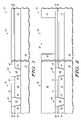
- FIG. 1Shown in FIG. 1 is a semiconductor device structure 10 comprising an insulating layer 12 , a semiconductor layer 14 on insulating layer 12 , a pad oxide layer 16 on semiconductor layer 14 , and a nitride layer 18 .
- Semiconductor device structure 10is divided into an optical device region 20 and an electronic device region 22 .
- optical device region 20is for forming a waveguide and electronic device region 22 is for forming a transistor.
- Optical device region 20has an opening 24 and an opening 26 . Openings 24 and 26 extend to insulating layer 12 .
- Semiconductor layer 14is preferably monocrystalline silicon that is on the order of about 700 Angstroms thick.
- insulating layer 12includes oxide of on the order of about 8000 Angstroms or greater in thickness on a relatively thick silicon substrate (not shown). The exact thickness is determined by the particular optical device requirements. Insulating layer 12 and semiconductor layer 14 together in this described manner are similar to a standard semiconductor on insulator (SOI) wafer except that in this case insulating layer 12 is thicker than the corresponding buried oxide layer in a conventional SOI wafer.
- SOIsemiconductor on insulator
- optical region 20is masked so that no openings are formed in optical region 20 . Openings such as openings 24 and 26 are often called trenches.
- Pad oxide 16 and nitride 18are conventional layers used in preparation for trench formation.
- a conventional trench fillis performed, preferably with high density plasma (HDP) oxide as shown in regions 36 and 38 .
- CMPis performed to complete a conventional shallow trench isolation (STI) process module.
- a layer of photoresist 40is deposited and patterned using photolithography on the wafer, thus creating an opening 42 over optics region 20 .
- the photoresistcould include a single spin-on resist or a stack of an anti-reflection coating and photoresist.
- a portion of pad oxide 16 and nitride 18are removed with an etching step in region 42 to form an opening 44 in optical device region 20 .
- the photoresist 40is subsequently removed.
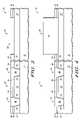
- siliconis selectively epitaxially grown in open region 44 , using film stack 18 , 16 as the selective growth window.
- the epitaxial growthis intended to thicken the silicon layer to a total of approximately 3000 angstroms.
- the actual final silicon film thicknessis determined by the particular device requirements of the optical device.
- the resultant grown siliconis depicted as region 46 .
- epitaxial growthrequires careful pre-treatment to ensure that the silicon surface is clean and free of native oxide prior to growth. Such cleans may consist of a high temperature hydrogen bake. Such a heat cycle may not desirable after diffusions are formed in a transistor flow, and thus, this embodiment favorably places the epitaxial process prior to well formation in the standard electronics flow.
- the nitride etchpreferably includes a dry etch stopping on oxide 16 in the electronics region 22 and silicon in optics region 20 .
- FIG. 6standard semiconductor processing is followed to build the devices in electronics region 22 , up through gate electrode deposition. Not shown, for simplicity, are the well implants in this region, which could be masked from optics region 20 .
- a gate dielectric 48is grown or deposited across the entire structure and then a gate electrode material 50 is deposited on top of the gate dielectric.
- the gate dielectric 48could be formed either by a first, thick gate thermal oxidation followed by a strip or patterned strip and then followed by a subsequent or multiple repetitions of gate oxidations depending upon the specific electronic or optical device needs.
- FIG. 7Shown in FIG. 7 is the structure following the patterning and etching of the gate electrode material 50 in region 22 to form the gate electrode 52 . Note that the gate electrode material is completely removed from the top of the optics region 20 .
- FIG. 8Shown in FIG. 8 is the semiconductor device structure 10 through spacer formation in electronic region 22 using conventional means.
- the transistorcomprises gate dielectric 48 over semiconductor layer 14 and etched gate electrode 52 over gate dielectric 48 .
- Source/drain extensions 54are formed through ion implantation.
- a spacer liner 56is deposited everywhere and a sidewall spacer 58 is formed around gate 52 by etching of the spacer material 58 to stop on the spacer liner 56 .
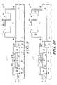
- semiconductor device structure 10Shown in FIG. 9 is semiconductor device structure 10 after formation of trenches 60 and 62 in the epitaxially grown silicon 46 within optics region 20 .
- regions over epitaxial silicon 46are opened and portions of liner 56 and silicon layer 46 are subsequently etched using a conventional timed silicon etch.
- the etch depthcan be selected according the particular optical device requirements but would, in this embodiment, be about 1500 angstroms.
- semiconductor device structure 10after formation of source/drain diffusions 64 , 65 , 66 and 67 in electronics region 22 and optional contact diffusions 68 and 70 in optical device region 20 and subsequent annealing.
- Such featurescan be formed by ion implantation and annealed with any thermal process with rapid thermal annealing being preferable.
- semiconductor device structure 10after deposition of a dielectric layer 72 intended as a salicide block layer.
- FIG. 12Shown in FIG. 12 is semiconductor device structure 10 after selective removal of the salicide blocking film 72 and spacer liner oxide 56 over the exposed active regions 14 and gate electrode regions 52 .
- the remainder of the film, 72will be present over the entirety of the optical device region 20 as shown for simplicity in the accompanying figures, but may be removed in portions of the optical region 20 where contact diffusions are connected to the upper metallization (not shown in FIG. 12 ).
- FIG. 13Shown in FIG. 13 is semiconductor device structure 10 after the formation of a salicide 74 and subsequent interlayer dielectric deposition 76 and planarization.
- the salicideis formed through standard means by depositing a metal, preferably cobalt or nickel with a Ti of TiN cap, annealing to form a reaction between the metal and silicon 14 in contact with the metal and etching to remove unreacted metal. Additional heat cycles may be used in this process.
- Film 72specifically prevents such a salicide from forming in the optical region where it might otherwise induce unacceptable optical losses.
- An interlayer dielectric film 76 or stack of filmsis deposited which simultaneously forms the side and upper cladding layers for optical devices in optical device portion 20 . Subsequent to this step, contacts and metallizations are formed as in a conventional electronics process.
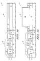
- FIG. 14Shown in FIG. 14 is the device 10 in another embodiment of the present invention, wherein the epitaxial growth is not formed until after electronic device spacer deposition.
- This embodimentis motivated by the requirement of high-performance CMOS to have a planar surface prior to gate electrode patterning, thus enabling tight design rules and aggressive critical dimensions.
- a large exclusion regionmay be required between the optics and electronics portions of the chip.
- Standard electronics processing for the formation of high performance electronicsis followed through spacer deposition.
- the electronics portion 22is as it would be just prior to the spacer etch shown in FIG. 8 .
- the optics portionremains as active silicon.
- liner dielectric 56is shown to overlay the entire structure and spacer material, preferably a nitride, 57 is shown to overly the liner dielectric 56 .
- an openingis patterned using photolithographic and etch techniques in the liner 56 and spacer film 57 in optics region 20 of the device.
- the entirety of electronics portion 22is protected from this etch by photoresist.
- the photoresistis removed everywhere and the remainder of the layers 56 and 57 form a hardmask to define a region over the optics region 20 of the circuit for selective epitaxial growth.
- Approximately 2300 angstroms of siliconis grown in the opening in layers 56 and 57 to form a totality of about 3000 angstroms as region 80 .
- the exact final thickness of the silicon 80is determined by the specific device requirements on the optical device.
- spacer material 57is etched to form sidewall spacers 58 in the electronics portion of the device. This etch would be performed selectively using a photoresist mask to protect the optics portion of the device. Subsequent processing would continue as indicated on FIG. 9 with the exception that liner film 56 would not be present on the optical portion of the device and the remainder of liner and spacer material 56 and 57 would exist as the boundary of the window within which the epitaxial material ( 46 in embodiment 1 and 80 in embodiment 2 ) was grown. Likewise, the remainder of the process would follow FIGS. 10 , 11 , 12 and 13 with the same modifications to the drawings.
Landscapes
- Metal-Oxide And Bipolar Metal-Oxide Semiconductor Integrated Circuits (AREA)
- Optical Integrated Circuits (AREA)
- Electrodes Of Semiconductors (AREA)
- Solid State Image Pick-Up Elements (AREA)
Abstract
Description
Claims (37)
Priority Applications (4)
| Application Number | Priority Date | Filing Date | Title |
|---|---|---|---|
| US10/989,940US7109051B2 (en) | 2004-11-15 | 2004-11-15 | Method of integrating optical devices and electronic devices on an integrated circuit |
| PCT/US2005/041155WO2006055476A2 (en) | 2004-11-15 | 2005-11-14 | Method of integrating optical devices and electronic devices on an integrated circuit |
| EP05822578AEP1854128A4 (en) | 2004-11-15 | 2005-11-14 | METHOD FOR INTEGRATING OPTICAL DEVICES AND ELECTRONIC DEVICES ON AN INTEGRATED CIRCUIT |
| JP2007541397AJP5107049B2 (en) | 2004-11-15 | 2005-11-14 | Method for integrating an optical device and an electronic device on an integrated circuit |
Applications Claiming Priority (1)
| Application Number | Priority Date | Filing Date | Title |
|---|---|---|---|
| US10/989,940US7109051B2 (en) | 2004-11-15 | 2004-11-15 | Method of integrating optical devices and electronic devices on an integrated circuit |
Publications (2)
| Publication Number | Publication Date |
|---|---|
| US20060105479A1 US20060105479A1 (en) | 2006-05-18 |
| US7109051B2true US7109051B2 (en) | 2006-09-19 |
Family
ID=36386883
Family Applications (1)
| Application Number | Title | Priority Date | Filing Date |
|---|---|---|---|
| US10/989,940Expired - Fee RelatedUS7109051B2 (en) | 2004-11-15 | 2004-11-15 | Method of integrating optical devices and electronic devices on an integrated circuit |
Country Status (4)
| Country | Link |
|---|---|
| US (1) | US7109051B2 (en) |
| EP (1) | EP1854128A4 (en) |
| JP (1) | JP5107049B2 (en) |
| WO (1) | WO2006055476A2 (en) |
Cited By (13)
| Publication number | Priority date | Publication date | Assignee | Title |
|---|---|---|---|---|
| US20060266081A1 (en)* | 2002-10-23 | 2006-11-30 | Applied Materials, Inc. | Method of forming a phosphorus doped optical core using a pecvd process |
| US20100059802A1 (en)* | 2008-09-11 | 2010-03-11 | Shenlin Chen | Image sensor with raised photosensitive elements |
| US7785983B2 (en) | 2007-03-07 | 2010-08-31 | Freescale Semiconductor, Inc. | Semiconductor device having tiles for dual-trench integration and method therefor |
| US8139130B2 (en) | 2005-07-28 | 2012-03-20 | Omnivision Technologies, Inc. | Image sensor with improved light sensitivity |
| US8194296B2 (en) | 2006-05-22 | 2012-06-05 | Omnivision Technologies, Inc. | Image sensor with improved light sensitivity |
| US8274715B2 (en) | 2005-07-28 | 2012-09-25 | Omnivision Technologies, Inc. | Processing color and panchromatic pixels |
| US20120322177A1 (en)* | 2010-12-03 | 2012-12-20 | Bae Systems Information And Electronic Systems Integration Inc. | Method of integrating slotted waveguide into cmos process |
| US8416339B2 (en) | 2006-10-04 | 2013-04-09 | Omni Vision Technologies, Inc. | Providing multiple video signals from single sensor |
| US20140212087A1 (en)* | 2013-01-25 | 2014-07-31 | Samsung Electronics Co., Ltd | Semiconductor apparatus including an optical device and an electronic device, and method of manufacturing the same |
| US8951882B2 (en)* | 2012-11-21 | 2015-02-10 | Samsung Electronics Co., Ltd. | Method of fabricating optoelectronic integrated circuit substrate |
| US9018108B2 (en) | 2013-01-25 | 2015-04-28 | Applied Materials, Inc. | Low shrinkage dielectric films |
| US20170097468A1 (en)* | 2012-11-30 | 2017-04-06 | International Business Machines Corporation | Semiconductor structure and method for manufacturing a semiconductor structure |
| US11526037B2 (en)* | 2018-10-17 | 2022-12-13 | Samsung Electronics Co., Ltd. | Semiconductor device |
Families Citing this family (15)
| Publication number | Priority date | Publication date | Assignee | Title |
|---|---|---|---|---|
| US7574090B2 (en)* | 2006-05-12 | 2009-08-11 | Toshiba America Electronic Components, Inc. | Semiconductor device using buried oxide layer as optical wave guides |
| US9137262B2 (en) | 2011-10-11 | 2015-09-15 | Citrix Systems, Inc. | Providing secure mobile device access to enterprise resources using application tunnels |
| US9280377B2 (en) | 2013-03-29 | 2016-03-08 | Citrix Systems, Inc. | Application with multiple operation modes |
| US9599561B2 (en) | 2011-10-13 | 2017-03-21 | Affymetrix, Inc. | Methods, systems and apparatuses for testing and calibrating fluorescent scanners |
| US8910239B2 (en) | 2012-10-15 | 2014-12-09 | Citrix Systems, Inc. | Providing virtualized private network tunnels |
| CN104854561B (en) | 2012-10-16 | 2018-05-11 | 思杰系统有限公司 | Application wrapper for application management framework |
| US9971585B2 (en) | 2012-10-16 | 2018-05-15 | Citrix Systems, Inc. | Wrapping unmanaged applications on a mobile device |
| US9595629B2 (en)* | 2012-10-22 | 2017-03-14 | Mellanox Technologies Silicon Photonics Inc. | Enhancing planarization uniformity in optical devices |
| US9387815B2 (en) | 2013-02-28 | 2016-07-12 | Kevin Goldstein | Apparatus for collection of debris escaping around a vehicle tailgate |
| US9413736B2 (en) | 2013-03-29 | 2016-08-09 | Citrix Systems, Inc. | Providing an enterprise application store |
| US9985850B2 (en) | 2013-03-29 | 2018-05-29 | Citrix Systems, Inc. | Providing mobile device management functionalities |
| US9355223B2 (en) | 2013-03-29 | 2016-05-31 | Citrix Systems, Inc. | Providing a managed browser |
| US10284627B2 (en) | 2013-03-29 | 2019-05-07 | Citrix Systems, Inc. | Data management for an application with multiple operation modes |
| WO2015050167A1 (en)* | 2013-10-02 | 2015-04-09 | 技術研究組合光電子融合基盤技術研究所 | Semiconductor integrated circuit and method for manufacturing same |
| US10884192B1 (en)* | 2019-12-16 | 2021-01-05 | Hewlett Packard Enterprise Development Lp | Single-etch wide-bandwidth grating couplers with individually-tuned grating sections |
Citations (23)
| Publication number | Priority date | Publication date | Assignee | Title |
|---|---|---|---|---|
| US3569997A (en)* | 1967-07-13 | 1971-03-09 | Inventors And Investors Inc | Photoelectric microcircuit components monolythically integrated with zone plate optics |
| US5612231A (en)* | 1994-05-09 | 1997-03-18 | Motorola | Method of fabricating an electro-optic integrated circuit having light emitting diodes |
| US5674778A (en)* | 1994-11-08 | 1997-10-07 | Samsung Electronics Co., Ltd. | Method of manufacturing an optoelectronic circuit including heterojunction bipolar transistor, laser and photodetector |
| US5885847A (en)* | 1996-12-06 | 1999-03-23 | Electronics And Telecommunications Research Institute | Method of fabricating a compound semiconductor device |
| US5937274A (en)* | 1995-01-31 | 1999-08-10 | Hitachi, Ltd. | Fabrication method for AlGaIn NPAsSb based devices |
| US5963788A (en)* | 1995-09-06 | 1999-10-05 | Sandia Corporation | Method for integrating microelectromechanical devices with electronic circuitry |
| US6096591A (en)* | 1997-06-30 | 2000-08-01 | Advanced Micro Devices, Inc. | Method of making an IGFET and a protected resistor with reduced processing steps |
| WO2002014915A2 (en) | 2000-08-17 | 2002-02-21 | Mcmaster University | Silicon-on-insulator optical waveguide fabrication by local oxidation of silicon |
| US6458614B1 (en)* | 1998-03-26 | 2002-10-01 | Murata Manufacturing Co., | Opto-electronic integrated circuit |
| US20020164122A1 (en) | 2001-05-02 | 2002-11-07 | Taylor William J. | Opto-coupling device structure and method therefor |
| WO2003023476A1 (en) | 2001-09-10 | 2003-03-20 | California Institute Of Technology | Tuning the index of a waveguide structure |
| WO2003023469A1 (en) | 2001-09-10 | 2003-03-20 | California Institue Of Technology | Strip loaded waveguide integrated with electronics components |
| US6585424B2 (en)* | 2001-07-25 | 2003-07-01 | Motorola, Inc. | Structure and method for fabricating an electro-rheological lens |
| US6608945B2 (en) | 2001-05-17 | 2003-08-19 | Optronx, Inc. | Self-aligning modulator method and associated apparatus |
| US6654511B2 (en) | 2001-05-17 | 2003-11-25 | Sioptical, Inc. | Optical modulator apparatus and associated method |
| US20030235370A1 (en) | 2002-04-10 | 2003-12-25 | Interuniversitair Microelektronica Centrum (Imec Vzw) | Fiber-to-waveguide coupler |
| US20040002177A1 (en)* | 2002-06-26 | 2004-01-01 | Liang-Hua Lin | Photo sensor and method of forming the same |
| US6687446B2 (en) | 2000-06-28 | 2004-02-03 | Oki Electric Industry Co., Ltd. | Optical waveguide device and manufacturing method therefor |
| US6746948B2 (en)* | 2001-09-17 | 2004-06-08 | Matsushita Electric Industrial Co., Ltd. | Method for fabricating semiconductor light-emitting device |
| US20050054131A1 (en)* | 2003-07-23 | 2005-03-10 | Applied Materials, Inc. | Solution to thermal budget |
| US20050214989A1 (en)* | 2004-03-29 | 2005-09-29 | Honeywell International Inc. | Silicon optoelectronic device |
| US6968110B2 (en)* | 2003-04-21 | 2005-11-22 | Sioptical, Inc. | CMOS-compatible integration of silicon-based optical devices with electronic devices |
| US20050260802A1 (en)* | 2004-04-07 | 2005-11-24 | Andrea Pizzarulli | SOI circuit having reduced crosstalk interference and a method for forming the same |
Family Cites Families (1)
| Publication number | Priority date | Publication date | Assignee | Title |
|---|---|---|---|---|
| EP1107044A1 (en)* | 1999-11-30 | 2001-06-13 | Hitachi Europe Limited | Photonic device |
- 2004
- 2004-11-15USUS10/989,940patent/US7109051B2/ennot_activeExpired - Fee Related
- 2005
- 2005-11-14WOPCT/US2005/041155patent/WO2006055476A2/enactiveApplication Filing
- 2005-11-14JPJP2007541397Apatent/JP5107049B2/ennot_activeExpired - Fee Related
- 2005-11-14EPEP05822578Apatent/EP1854128A4/ennot_activeCeased
Patent Citations (24)
| Publication number | Priority date | Publication date | Assignee | Title |
|---|---|---|---|---|
| US3569997A (en)* | 1967-07-13 | 1971-03-09 | Inventors And Investors Inc | Photoelectric microcircuit components monolythically integrated with zone plate optics |
| US5612231A (en)* | 1994-05-09 | 1997-03-18 | Motorola | Method of fabricating an electro-optic integrated circuit having light emitting diodes |
| US5674778A (en)* | 1994-11-08 | 1997-10-07 | Samsung Electronics Co., Ltd. | Method of manufacturing an optoelectronic circuit including heterojunction bipolar transistor, laser and photodetector |
| US5937274A (en)* | 1995-01-31 | 1999-08-10 | Hitachi, Ltd. | Fabrication method for AlGaIn NPAsSb based devices |
| US5963788A (en)* | 1995-09-06 | 1999-10-05 | Sandia Corporation | Method for integrating microelectromechanical devices with electronic circuitry |
| US5885847A (en)* | 1996-12-06 | 1999-03-23 | Electronics And Telecommunications Research Institute | Method of fabricating a compound semiconductor device |
| US6096591A (en)* | 1997-06-30 | 2000-08-01 | Advanced Micro Devices, Inc. | Method of making an IGFET and a protected resistor with reduced processing steps |
| US6458614B1 (en)* | 1998-03-26 | 2002-10-01 | Murata Manufacturing Co., | Opto-electronic integrated circuit |
| US6687446B2 (en) | 2000-06-28 | 2004-02-03 | Oki Electric Industry Co., Ltd. | Optical waveguide device and manufacturing method therefor |
| WO2002014915A2 (en) | 2000-08-17 | 2002-02-21 | Mcmaster University | Silicon-on-insulator optical waveguide fabrication by local oxidation of silicon |
| US20020164122A1 (en) | 2001-05-02 | 2002-11-07 | Taylor William J. | Opto-coupling device structure and method therefor |
| US6654511B2 (en) | 2001-05-17 | 2003-11-25 | Sioptical, Inc. | Optical modulator apparatus and associated method |
| US6608945B2 (en) | 2001-05-17 | 2003-08-19 | Optronx, Inc. | Self-aligning modulator method and associated apparatus |
| US6585424B2 (en)* | 2001-07-25 | 2003-07-01 | Motorola, Inc. | Structure and method for fabricating an electro-rheological lens |
| US20030063885A1 (en) | 2001-09-10 | 2003-04-03 | Gunn Lawrence Cary | Electronically biased strip loaded waveguide |
| WO2003023469A1 (en) | 2001-09-10 | 2003-03-20 | California Institue Of Technology | Strip loaded waveguide integrated with electronics components |
| WO2003023476A1 (en) | 2001-09-10 | 2003-03-20 | California Institute Of Technology | Tuning the index of a waveguide structure |
| US6746948B2 (en)* | 2001-09-17 | 2004-06-08 | Matsushita Electric Industrial Co., Ltd. | Method for fabricating semiconductor light-emitting device |
| US20030235370A1 (en) | 2002-04-10 | 2003-12-25 | Interuniversitair Microelektronica Centrum (Imec Vzw) | Fiber-to-waveguide coupler |
| US20040002177A1 (en)* | 2002-06-26 | 2004-01-01 | Liang-Hua Lin | Photo sensor and method of forming the same |
| US6968110B2 (en)* | 2003-04-21 | 2005-11-22 | Sioptical, Inc. | CMOS-compatible integration of silicon-based optical devices with electronic devices |
| US20050054131A1 (en)* | 2003-07-23 | 2005-03-10 | Applied Materials, Inc. | Solution to thermal budget |
| US20050214989A1 (en)* | 2004-03-29 | 2005-09-29 | Honeywell International Inc. | Silicon optoelectronic device |
| US20050260802A1 (en)* | 2004-04-07 | 2005-11-24 | Andrea Pizzarulli | SOI circuit having reduced crosstalk interference and a method for forming the same |
Non-Patent Citations (1)
| Title |
|---|
| Fischer et al., "0.1 dB/cm Waveguide Losses in Single-Mode SOI Rib Waveguides," IEEE Photonics Technology Letters, vol. 8, No. 5, May 1996, pp. 647-648. |
Cited By (20)
| Publication number | Priority date | Publication date | Assignee | Title |
|---|---|---|---|---|
| US7325419B2 (en)* | 2002-10-23 | 2008-02-05 | Applied Materials, Inc. | Method of forming a phosphorus doped optical core using a PECVD process |
| US20060266081A1 (en)* | 2002-10-23 | 2006-11-30 | Applied Materials, Inc. | Method of forming a phosphorus doped optical core using a pecvd process |
| US8274715B2 (en) | 2005-07-28 | 2012-09-25 | Omnivision Technologies, Inc. | Processing color and panchromatic pixels |
| US8711452B2 (en) | 2005-07-28 | 2014-04-29 | Omnivision Technologies, Inc. | Processing color and panchromatic pixels |
| US8139130B2 (en) | 2005-07-28 | 2012-03-20 | Omnivision Technologies, Inc. | Image sensor with improved light sensitivity |
| US8330839B2 (en) | 2005-07-28 | 2012-12-11 | Omnivision Technologies, Inc. | Image sensor with improved light sensitivity |
| US8194296B2 (en) | 2006-05-22 | 2012-06-05 | Omnivision Technologies, Inc. | Image sensor with improved light sensitivity |
| US8416339B2 (en) | 2006-10-04 | 2013-04-09 | Omni Vision Technologies, Inc. | Providing multiple video signals from single sensor |
| US7785983B2 (en) | 2007-03-07 | 2010-08-31 | Freescale Semiconductor, Inc. | Semiconductor device having tiles for dual-trench integration and method therefor |
| US8211732B2 (en)* | 2008-09-11 | 2012-07-03 | Omnivision Technologies, Inc. | Image sensor with raised photosensitive elements |
| US8525241B2 (en) | 2008-09-11 | 2013-09-03 | Omni Vision Technologies, Inc. | Image sensor with raised photosensitive elements |
| US20100059802A1 (en)* | 2008-09-11 | 2010-03-11 | Shenlin Chen | Image sensor with raised photosensitive elements |
| US20120322177A1 (en)* | 2010-12-03 | 2012-12-20 | Bae Systems Information And Electronic Systems Integration Inc. | Method of integrating slotted waveguide into cmos process |
| US8513037B2 (en)* | 2010-12-03 | 2013-08-20 | Bae Systems Information And Electronic Systems Integration Inc. | Method of integrating slotted waveguide into CMOS process |
| US8951882B2 (en)* | 2012-11-21 | 2015-02-10 | Samsung Electronics Co., Ltd. | Method of fabricating optoelectronic integrated circuit substrate |
| US20170097468A1 (en)* | 2012-11-30 | 2017-04-06 | International Business Machines Corporation | Semiconductor structure and method for manufacturing a semiconductor structure |
| US9989703B2 (en)* | 2012-11-30 | 2018-06-05 | International Business Machines Corporation | Semiconductor structure and method for manufacturing a semiconductor structure |
| US20140212087A1 (en)* | 2013-01-25 | 2014-07-31 | Samsung Electronics Co., Ltd | Semiconductor apparatus including an optical device and an electronic device, and method of manufacturing the same |
| US9018108B2 (en) | 2013-01-25 | 2015-04-28 | Applied Materials, Inc. | Low shrinkage dielectric films |
| US11526037B2 (en)* | 2018-10-17 | 2022-12-13 | Samsung Electronics Co., Ltd. | Semiconductor device |
Also Published As
| Publication number | Publication date |
|---|---|
| JP5107049B2 (en) | 2012-12-26 |
| WO2006055476A2 (en) | 2006-05-26 |
| WO2006055476A3 (en) | 2009-05-14 |
| EP1854128A2 (en) | 2007-11-14 |
| US20060105479A1 (en) | 2006-05-18 |
| EP1854128A4 (en) | 2010-12-15 |
| JP2008521216A (en) | 2008-06-19 |
Similar Documents
| Publication | Publication Date | Title |
|---|---|---|
| US7109051B2 (en) | Method of integrating optical devices and electronic devices on an integrated circuit | |
| US5635746A (en) | Semiconductor device comprising a salicide structure | |
| TWI573267B (en) | Semiconductor device and method of fabricating non-planar circuit device | |
| US11164980B2 (en) | Silicon photonics integration method and structure | |
| US9229164B2 (en) | Butt-coupled buried waveguide photodetector | |
| US7820500B2 (en) | Single mask scheme method and structure for integrating PMOS and NMOS transistors using strained silicon | |
| US7169654B2 (en) | Method of forming a semiconductor device | |
| US20110158582A1 (en) | Structure of a semiconductor device having a waveguide and method of forming the same | |
| TWI283481B (en) | BiCMOS integration scheme with raised extrinsic base | |
| KR20060040711A (en) | Solution for Thermal Budget | |
| US7098090B2 (en) | Method of forming a semiconductor device | |
| US5985725A (en) | Method for manufacturing dual gate oxide layer | |
| US6979651B1 (en) | Method for forming alignment features and back-side contacts with fewer lithography and etch steps | |
| US7067342B2 (en) | Method of integrating optical devices and electronic devices on an integrated circuit | |
| KR20010107707A (en) | Method for manufacturing semiconductor device having a sti structure | |
| KR100849077B1 (en) | Method of manufacturing system on chip device | |
| JPH0368170A (en) | Manufacture of thin film semiconductor element | |
| KR100240096B1 (en) | Method for manufacturing semiconductor device | |
| KR100864933B1 (en) | Manufacturing Method of Semiconductor Device | |
| KR100881494B1 (en) | Manufacturing method of semiconductor device | |
| TW200410339A (en) | Mask with extended mask clear-out window and method of dummy exposure using the same | |
| KR100516228B1 (en) | Method For Manufacturing Semiconductor Device | |
| KR101030298B1 (en) | Method of manufacturing a stacked gate flash memory device | |
| US20090263960A1 (en) | Semiconductor device with recess gate and method of fabricating the same | |
| KR20030049560A (en) | Method for manufacturing semiconductor device |
Legal Events
| Date | Code | Title | Description |
|---|---|---|---|
| AS | Assignment | Owner name:FREESCALE SEMICONDUCTOR, INC., TEXAS Free format text:ASSIGNMENT OF ASSIGNORS INTEREST;ASSIGNORS:CAVE, NIGEL G.;ZIA, OMAR;REEL/FRAME:015905/0422 Effective date:20050311 | |
| AS | Assignment | Owner name:CITIBANK, N.A. AS COLLATERAL AGENT, NEW YORK Free format text:SECURITY AGREEMENT;ASSIGNORS:FREESCALE SEMICONDUCTOR, INC.;FREESCALE ACQUISITION CORPORATION;FREESCALE ACQUISITION HOLDINGS CORP.;AND OTHERS;REEL/FRAME:018855/0129 Effective date:20061201 Owner name:CITIBANK, N.A. AS COLLATERAL AGENT,NEW YORK Free format text:SECURITY AGREEMENT;ASSIGNORS:FREESCALE SEMICONDUCTOR, INC.;FREESCALE ACQUISITION CORPORATION;FREESCALE ACQUISITION HOLDINGS CORP.;AND OTHERS;REEL/FRAME:018855/0129 Effective date:20061201 | |
| FPAY | Fee payment | Year of fee payment:4 | |
| AS | Assignment | Owner name:CITIBANK, N.A., AS COLLATERAL AGENT,NEW YORK Free format text:SECURITY AGREEMENT;ASSIGNOR:FREESCALE SEMICONDUCTOR, INC.;REEL/FRAME:024397/0001 Effective date:20100413 Owner name:CITIBANK, N.A., AS COLLATERAL AGENT, NEW YORK Free format text:SECURITY AGREEMENT;ASSIGNOR:FREESCALE SEMICONDUCTOR, INC.;REEL/FRAME:024397/0001 Effective date:20100413 | |
| AS | Assignment | Owner name:CITIBANK, N.A., AS NOTES COLLATERAL AGENT, NEW YORK Free format text:SECURITY AGREEMENT;ASSIGNOR:FREESCALE SEMICONDUCTOR, INC.;REEL/FRAME:030633/0424 Effective date:20130521 Owner name:CITIBANK, N.A., AS NOTES COLLATERAL AGENT, NEW YOR Free format text:SECURITY AGREEMENT;ASSIGNOR:FREESCALE SEMICONDUCTOR, INC.;REEL/FRAME:030633/0424 Effective date:20130521 | |
| AS | Assignment | Owner name:CITIBANK, N.A., AS NOTES COLLATERAL AGENT, NEW YORK Free format text:SECURITY AGREEMENT;ASSIGNOR:FREESCALE SEMICONDUCTOR, INC.;REEL/FRAME:031591/0266 Effective date:20131101 Owner name:CITIBANK, N.A., AS NOTES COLLATERAL AGENT, NEW YOR Free format text:SECURITY AGREEMENT;ASSIGNOR:FREESCALE SEMICONDUCTOR, INC.;REEL/FRAME:031591/0266 Effective date:20131101 | |
| FPAY | Fee payment | Year of fee payment:8 | |
| AS | Assignment | Owner name:FREESCALE SEMICONDUCTOR, INC., TEXAS Free format text:PATENT RELEASE;ASSIGNOR:CITIBANK, N.A., AS COLLATERAL AGENT;REEL/FRAME:037354/0225 Effective date:20151207 Owner name:FREESCALE SEMICONDUCTOR, INC., TEXAS Free format text:PATENT RELEASE;ASSIGNOR:CITIBANK, N.A., AS COLLATERAL AGENT;REEL/FRAME:037356/0143 Effective date:20151207 Owner name:FREESCALE SEMICONDUCTOR, INC., TEXAS Free format text:PATENT RELEASE;ASSIGNOR:CITIBANK, N.A., AS COLLATERAL AGENT;REEL/FRAME:037356/0553 Effective date:20151207 | |
| AS | Assignment | Owner name:MORGAN STANLEY SENIOR FUNDING, INC., MARYLAND Free format text:ASSIGNMENT AND ASSUMPTION OF SECURITY INTEREST IN PATENTS;ASSIGNOR:CITIBANK, N.A.;REEL/FRAME:037486/0517 Effective date:20151207 | |
| AS | Assignment | Owner name:MORGAN STANLEY SENIOR FUNDING, INC., MARYLAND Free format text:ASSIGNMENT AND ASSUMPTION OF SECURITY INTEREST IN PATENTS;ASSIGNOR:CITIBANK, N.A.;REEL/FRAME:037518/0292 Effective date:20151207 | |
| AS | Assignment | Owner name:NORTH STAR INNOVATIONS INC., CALIFORNIA Free format text:ASSIGNMENT OF ASSIGNORS INTEREST;ASSIGNOR:FREESCALE SEMICONDUCTOR, INC.;REEL/FRAME:037694/0264 Effective date:20151002 | |
| AS | Assignment | Owner name:NXP, B.V., F/K/A FREESCALE SEMICONDUCTOR, INC., NETHERLANDS Free format text:RELEASE BY SECURED PARTY;ASSIGNOR:MORGAN STANLEY SENIOR FUNDING, INC.;REEL/FRAME:040925/0001 Effective date:20160912 Owner name:NXP, B.V., F/K/A FREESCALE SEMICONDUCTOR, INC., NE Free format text:RELEASE BY SECURED PARTY;ASSIGNOR:MORGAN STANLEY SENIOR FUNDING, INC.;REEL/FRAME:040925/0001 Effective date:20160912 | |
| AS | Assignment | Owner name:NXP B.V., NETHERLANDS Free format text:RELEASE BY SECURED PARTY;ASSIGNOR:MORGAN STANLEY SENIOR FUNDING, INC.;REEL/FRAME:040928/0001 Effective date:20160622 | |
| AS | Assignment | Owner name:MORGAN STANLEY SENIOR FUNDING, INC., MARYLAND Free format text:CORRECTIVE ASSIGNMENT TO CORRECT THE REMOVE PATENTS 8108266 AND 8062324 AND REPLACE THEM WITH 6108266 AND 8060324 PREVIOUSLY RECORDED ON REEL 037518 FRAME 0292. ASSIGNOR(S) HEREBY CONFIRMS THE ASSIGNMENT AND ASSUMPTION OF SECURITY INTEREST IN PATENTS;ASSIGNOR:CITIBANK, N.A.;REEL/FRAME:041703/0536 Effective date:20151207 | |
| AS | Assignment | Owner name:TAIWAN SEMICONDUCTOR MANUFACTURING CO., LTD., TAIW Free format text:ASSIGNMENT OF ASSIGNORS INTEREST;ASSIGNOR:NORTH STAR INNOVATIONS INC.;REEL/FRAME:041717/0736 Effective date:20161006 | |
| FEPP | Fee payment procedure | Free format text:MAINTENANCE FEE REMINDER MAILED (ORIGINAL EVENT CODE: REM.) | |
| LAPS | Lapse for failure to pay maintenance fees | Free format text:PATENT EXPIRED FOR FAILURE TO PAY MAINTENANCE FEES (ORIGINAL EVENT CODE: EXP.); ENTITY STATUS OF PATENT OWNER: LARGE ENTITY | |
| STCH | Information on status: patent discontinuation | Free format text:PATENT EXPIRED DUE TO NONPAYMENT OF MAINTENANCE FEES UNDER 37 CFR 1.362 | |
| FP | Lapsed due to failure to pay maintenance fee | Effective date:20180919 | |
| AS | Assignment | Owner name:SHENZHEN XINGUODU TECHNOLOGY CO., LTD., CHINA Free format text:CORRECTIVE ASSIGNMENT TO CORRECT THE TO CORRECT THE APPLICATION NO. FROM 13,883,290 TO 13,833,290 PREVIOUSLY RECORDED ON REEL 041703 FRAME 0536. ASSIGNOR(S) HEREBY CONFIRMS THE THE ASSIGNMENT AND ASSUMPTION OF SECURITYINTEREST IN PATENTS.;ASSIGNOR:MORGAN STANLEY SENIOR FUNDING, INC.;REEL/FRAME:048734/0001 Effective date:20190217 | |
| AS | Assignment | Owner name:TAIWAN SEMICONDUCTOR MANUFACTURING CO., LTD., TAIWAN Free format text:323.01(C) ASSIGNMENT OR CHANGE OF NAME IMPROPERLY FILED AND RECORDED BY ANOTHER PERSON AGAINST OWNER'S PATENT;ASSIGNOR:TAIWAN SEMICONDUCTOR MANUFACTURING CO., LTD.;REEL/FRAME:052459/0656 Effective date:20190924 | |
| AS | Assignment | Owner name:MORGAN STANLEY SENIOR FUNDING, INC., MARYLAND Free format text:CORRECTIVE ASSIGNMENT TO CORRECT THE REMOVE APPLICATION11759915 AND REPLACE IT WITH APPLICATION 11759935 PREVIOUSLY RECORDED ON REEL 037486 FRAME 0517. ASSIGNOR(S) HEREBY CONFIRMS THE ASSIGNMENT AND ASSUMPTION OF SECURITYINTEREST IN PATENTS;ASSIGNOR:CITIBANK, N.A.;REEL/FRAME:053547/0421 Effective date:20151207 | |
| AS | Assignment | Owner name:NXP B.V., NETHERLANDS Free format text:CORRECTIVE ASSIGNMENT TO CORRECT THE REMOVEAPPLICATION 11759915 AND REPLACE IT WITH APPLICATION11759935 PREVIOUSLY RECORDED ON REEL 040928 FRAME 0001. ASSIGNOR(S) HEREBY CONFIRMS THE RELEASE OF SECURITYINTEREST;ASSIGNOR:MORGAN STANLEY SENIOR FUNDING, INC.;REEL/FRAME:052915/0001 Effective date:20160622 | |
| AS | Assignment | Owner name:NXP, B.V. F/K/A FREESCALE SEMICONDUCTOR, INC., NETHERLANDS Free format text:CORRECTIVE ASSIGNMENT TO CORRECT THE REMOVEAPPLICATION 11759915 AND REPLACE IT WITH APPLICATION11759935 PREVIOUSLY RECORDED ON REEL 040925 FRAME 0001. ASSIGNOR(S) HEREBY CONFIRMS THE RELEASE OF SECURITYINTEREST;ASSIGNOR:MORGAN STANLEY SENIOR FUNDING, INC.;REEL/FRAME:052917/0001 Effective date:20160912 |