US7108753B2 - Staggered ribs on process chamber to reduce thermal effects - Google Patents
Staggered ribs on process chamber to reduce thermal effectsDownload PDFInfo
- Publication number
- US7108753B2 US7108753B2US10/696,481US69648103AUS7108753B2US 7108753 B2US7108753 B2US 7108753B2US 69648103 AUS69648103 AUS 69648103AUS 7108753 B2US7108753 B2US 7108753B2
- Authority
- US
- United States
- Prior art keywords
- chamber
- ribs
- rearward
- reaction
- upper wall
- Prior art date
- Legal status (The legal status is an assumption and is not a legal conclusion. Google has not performed a legal analysis and makes no representation as to the accuracy of the status listed.)
- Expired - Lifetime, expires
Links
- 239000000758substrateSubstances0.000claims12
- 238000011144upstream manufacturingMethods0.000claims2
Images


Classifications
- C—CHEMISTRY; METALLURGY
- C23—COATING METALLIC MATERIAL; COATING MATERIAL WITH METALLIC MATERIAL; CHEMICAL SURFACE TREATMENT; DIFFUSION TREATMENT OF METALLIC MATERIAL; COATING BY VACUUM EVAPORATION, BY SPUTTERING, BY ION IMPLANTATION OR BY CHEMICAL VAPOUR DEPOSITION, IN GENERAL; INHIBITING CORROSION OF METALLIC MATERIAL OR INCRUSTATION IN GENERAL
- C23C—COATING METALLIC MATERIAL; COATING MATERIAL WITH METALLIC MATERIAL; SURFACE TREATMENT OF METALLIC MATERIAL BY DIFFUSION INTO THE SURFACE, BY CHEMICAL CONVERSION OR SUBSTITUTION; COATING BY VACUUM EVAPORATION, BY SPUTTERING, BY ION IMPLANTATION OR BY CHEMICAL VAPOUR DEPOSITION, IN GENERAL
- C23C16/00—Chemical coating by decomposition of gaseous compounds, without leaving reaction products of surface material in the coating, i.e. chemical vapour deposition [CVD] processes
- C23C16/44—Chemical coating by decomposition of gaseous compounds, without leaving reaction products of surface material in the coating, i.e. chemical vapour deposition [CVD] processes characterised by the method of coating
- C23C16/48—Chemical coating by decomposition of gaseous compounds, without leaving reaction products of surface material in the coating, i.e. chemical vapour deposition [CVD] processes characterised by the method of coating by irradiation, e.g. photolysis, radiolysis, particle radiation
- C23C16/481—Chemical coating by decomposition of gaseous compounds, without leaving reaction products of surface material in the coating, i.e. chemical vapour deposition [CVD] processes characterised by the method of coating by irradiation, e.g. photolysis, radiolysis, particle radiation by radiant heating of the substrate
- C—CHEMISTRY; METALLURGY
- C23—COATING METALLIC MATERIAL; COATING MATERIAL WITH METALLIC MATERIAL; CHEMICAL SURFACE TREATMENT; DIFFUSION TREATMENT OF METALLIC MATERIAL; COATING BY VACUUM EVAPORATION, BY SPUTTERING, BY ION IMPLANTATION OR BY CHEMICAL VAPOUR DEPOSITION, IN GENERAL; INHIBITING CORROSION OF METALLIC MATERIAL OR INCRUSTATION IN GENERAL
- C23C—COATING METALLIC MATERIAL; COATING MATERIAL WITH METALLIC MATERIAL; SURFACE TREATMENT OF METALLIC MATERIAL BY DIFFUSION INTO THE SURFACE, BY CHEMICAL CONVERSION OR SUBSTITUTION; COATING BY VACUUM EVAPORATION, BY SPUTTERING, BY ION IMPLANTATION OR BY CHEMICAL VAPOUR DEPOSITION, IN GENERAL
- C23C16/00—Chemical coating by decomposition of gaseous compounds, without leaving reaction products of surface material in the coating, i.e. chemical vapour deposition [CVD] processes
- C23C16/44—Chemical coating by decomposition of gaseous compounds, without leaving reaction products of surface material in the coating, i.e. chemical vapour deposition [CVD] processes characterised by the method of coating
- C—CHEMISTRY; METALLURGY
- C30—CRYSTAL GROWTH
- C30B—SINGLE-CRYSTAL GROWTH; UNIDIRECTIONAL SOLIDIFICATION OF EUTECTIC MATERIAL OR UNIDIRECTIONAL DEMIXING OF EUTECTOID MATERIAL; REFINING BY ZONE-MELTING OF MATERIAL; PRODUCTION OF A HOMOGENEOUS POLYCRYSTALLINE MATERIAL WITH DEFINED STRUCTURE; SINGLE CRYSTALS OR HOMOGENEOUS POLYCRYSTALLINE MATERIAL WITH DEFINED STRUCTURE; AFTER-TREATMENT OF SINGLE CRYSTALS OR A HOMOGENEOUS POLYCRYSTALLINE MATERIAL WITH DEFINED STRUCTURE; APPARATUS THEREFOR
- C30B25/00—Single-crystal growth by chemical reaction of reactive gases, e.g. chemical vapour-deposition growth
- C30B25/02—Epitaxial-layer growth
- C30B25/08—Reaction chambers; Selection of materials therefor
- C—CHEMISTRY; METALLURGY
- C30—CRYSTAL GROWTH
- C30B—SINGLE-CRYSTAL GROWTH; UNIDIRECTIONAL SOLIDIFICATION OF EUTECTIC MATERIAL OR UNIDIRECTIONAL DEMIXING OF EUTECTOID MATERIAL; REFINING BY ZONE-MELTING OF MATERIAL; PRODUCTION OF A HOMOGENEOUS POLYCRYSTALLINE MATERIAL WITH DEFINED STRUCTURE; SINGLE CRYSTALS OR HOMOGENEOUS POLYCRYSTALLINE MATERIAL WITH DEFINED STRUCTURE; AFTER-TREATMENT OF SINGLE CRYSTALS OR A HOMOGENEOUS POLYCRYSTALLINE MATERIAL WITH DEFINED STRUCTURE; APPARATUS THEREFOR
- C30B31/00—Diffusion or doping processes for single crystals or homogeneous polycrystalline material with defined structure; Apparatus therefor
- C30B31/06—Diffusion or doping processes for single crystals or homogeneous polycrystalline material with defined structure; Apparatus therefor by contacting with diffusion material in the gaseous state
- C30B31/10—Reaction chambers; Selection of materials therefor
Definitions
- This inventionrelates generally to semiconductor processing chambers, and relates more particularly in one embodiment to the positioning of ribs on exterior surfaces of a process chamber to reduce thermal effects within the process chamber.
- Process chambers for thermally processing semiconductor waferstypically are made of quartz (vitreous silica) or similar material because quartz is substantially transparent to radiant energy. Radiant heaters may be positioned adjacent the exterior of the chamber, and a wafer being processed in the chamber can be heated to elevated temperatures without having the chamber walls heated to the same level. Furthermore, quartz is desirable because it can withstand very high temperatures, and its inert characteristics enable it to withstand degradation by various processing gases.
- cylindrical or spherical chambersoften are preferred from a strength standpoint because their curved surfaces can best withstand the inwardly directed force.
- the chamber wallbe parallel to the facing flat surface of the wafer, to obtain uniform deposition on the wafer surface. Uniform deposition is critical to obtain a high yield of acceptable products to be made from such wafer.
- a flat wallwill collapse inwardly with reduced interior pressure sooner than will an outwardly convex wall of similar size and thickness.
- gussets or ribshave been provided on the exterior of the walls extending generally perpendicular to the wall to which they are joined, as may be seen in U.S. Pat. No. 4,920,918, issued on May 1, 1990, titled PRESSURE-RESISTANT THERMAL REACTOR SYSTEM FOR SEMICONDUCTOR PROCESSING, all of which is hereby incorporated by reference and made a part of this specification.
- One disadvantage of such a designis that even though quartz is substantially transparent to the radiant lamp energy, the ribs sections present a region of much thicker quartz, and thus the ribs locally absorb more lamp energy and attenuate the lamp energy delivered to the wafer. This attenuation of energy causes cooler regions (i.e., shadows) on the wafer.
- Such non-uniformity of temperature on the wafer surfacereduces the quality of the films that may be grown thereon, particularly for process conditions that are temperature-sensitive.
- Temperature non-uniformitiestypically may be somewhat reduced by rotating the wafer during processing. Rotation causes regions of the wafer that would otherwise reside within shadows all of the time to pass into warmer regions, as well. Thus, rotation tends to distribute temperatures of the wafer surface somewhat more uniformly. It has been found, however, that if the ribs positioned forward of the wafer center (i.e., the axis of rotation of the wafer) are located at approximately the same distance from the wafer center as are the ribs positioned rearward of the wafer center, temperature uniformity suffers even with rotation. Specifically, forward and rearward ribs positioned at relatively similar distances from the wafer center cause a combined shadowing effect on the surface of the rotating wafer which can result in temperature distributions that are more non-uniform than can otherwise be achieved.
- a semiconductor processing chamber having a plurality of ribs on an exterior surface of the chamberis provided.
- the ribsare positioned relative to the chamber such that shadows cast into the chamber by the ribs are offset from one another, thus more uniformly distributing radiant energy to the rotating wafer.
- the ribsare positioned on the exterior surface of the chamber so that they have dissimilar radial distances from a center of the chamber. This causes shadows produced by the ribs on a first side of the chamber to fall substantially between those shadows produced by the ribs on a second side of the chamber. Likewise, shadows produced by the ribs on the second side of the chamber fall substantially between the shadows produced by the ribs on the first side of the chamber.
- a chamberin one embodiment, comprises a chamber upper wall and a chamber lower wall. Each wall has an inner surface and an outer surface and defines an interior space therebetween.
- a plurality of forward ribsis provided on the outer surface of at least one of the chamber upper wall and chamber lower wall in a forward portion of the interior space. The forward portion is defined as forward of a central axis of the chamber.
- a plurality of rearward ribsis provided on the outer surface of at least one of the chamber upper wall and chamber lower wall in a rearward portion of the interior space. The rearward portion is defined as rearward of the central axis of the chamber.
- At least some of the forward ribsare positioned to have mirrored projections in the rearward portion of the chamber falling substantially between adjacent rearward ribs, and at least some of the rearward ribs are positioned to have mirrored projections in the forward portion of the chamber falling substantially between adjacent forward ribs.
- a reaction chamberin another embodiment, comprises a chamber upper wall and a chamber lower wall. Each wall has an inner surface and an outer surface and defining a reaction space therebetween.
- An inlet flangeis secured at a forward end of the chamber to the upper and lower walls.
- An outlet flangeis secured at a rearward end of the chamber to the upper and lower walls.
- a substrate supportis provided within the chamber space. The substrate support has a central axis around which the substrate support rotates.
- a radiant heat sourceis provided above the chamber, and a radiant heat source is provided below the chamber.
- a plurality of forward ribsare provided on the outer surface of the chamber upper wall and chamber lower wall.
- the forward ribsare located between the central axis of the substrate support and the inlet flange, wherein the forward ribs form a shadow onto the substrate support in a forward portion of the reaction space.
- a plurality of rearward ribsare provided on the outer surface of the chamber upper wall and chamber lower wall.
- the rearward ribsare located between the central axis of the substrate support and the outlet flange, wherein the rearward ribs form a shadow onto the substrate support in a rearward portion of the reaction space.
- a majority of the shadows formed by the forward ribshave a mirrored projection in the rearward portion of the reaction space that falls substantially between shadows of the rearward ribs.
- a majority of the shadows formed by the rearward ribshave a mirrored projection in the forward portion of the reaction space that falls substantially between shadows of the forward ribs.
- a reaction chambercomprising a chamber upper wall and a chamber lower wall. Each wall has an inner surface and an outer surface and defines a reaction space therebetween.
- a substrate supportis provided within the reaction space.
- the substrate supporthas a central axis around which the substrate support rotates.
- a plurality of forward ribsis provided on the outer surface of at least one of the chamber upper wall and chamber lower wall in a forward portion of the reaction space.
- a plurality of rearward ribsis provided on the outer surface of at least one of the chamber upper wall and chamber lower wall in a rearward portion of the reaction space. At least some of the forward ribs have a mirrored projection in the rearward portion of the reaction space that are approximately equidistant from adjacent rearward ribs. Likewise, at least some of the rearward ribs have a mirrored projection in the forward portion of the reaction space that are approximately equidistant from the adjacent forward ribs.
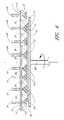
- FIG. 1is a perspective view of a semiconductor processing chamber having a plurality of ribs on exterior surfaces of the chamber.
- FIG. 1Ais a bottom elevation view of the processing chamber of FIG. 1 .
- FIG. 1Bis a partial cross-section view of the processing chamber of FIG. 1 , taken along line 1 B— 1 B.
- FIG. 2is a cross-sectional view of the semiconductor processing chamber of FIG. 1 , taken along line 2 — 2 .
- FIG. 3is a schematic view of the semiconductor processing chamber of FIG. 2 , illustrating the positions of the ribs relative to an axis of rotation of a susceptor and wafer within the chamber.
- FIG. 4is a schematic view illustrating shadows cast on the susceptor and wafer by several of the ribs on an upper surface of the chamber.
- FIGS. 1–1Billustrate one embodiment of a reactor vessel or chamber 10 for chemical vapor processing.
- the chamber 10has an elongated, generally flattened configuration.
- the chamber 10has an upper wall 14 with an outer surface 13 and an inner surface 13 ′, and a lower wall 16 with an outer surface 15 and an inner surface 15 ′.
- the walls 14 , 16are connected by vertically short side walls 11 and 12 .
- the walls 11 , 12 , 14 , 16are joined by an upstream inlet flange 17 and a downstream outlet flange 18 . Upstream and downstream relate to the direction of process gas flow through the chamber 10 and are synonymous in the present description with front and rear, as well as with frontward and rearward.
- the chamber 10can have configurations other than the flattened configuration shown in FIGS. 1–1B .
- the chamber 10can have tent-shaped cross-sectional shape, wherein the upper wall 14 and/or the lower wall 16 has a peak.
- the upper/lower walls 14 , 16can be rounded, giving the chamber 10 a generally ovoid cross-sectional shape.
- the upper/lower walls 14 , 16 of the chamber 10can be formed having other shapes in addition to the shapes discussed above, as well as combinations thereof.
- the chamber heightis less than the chamber width.
- a longitudinal direction for the chamber 10extends from the inlet flange 17 to the outlet flange 18 , or along the section line 2 — 2 .
- a lateral directionextends between the side walls 11 , 12 , or transversely to section line 2 — 2 .
- the height directionis perpendicular to both the longitudinal and lateral axes.
- the chamber 10has a length of about 300 mm, a width of about 206 mm, and a height of about 66.7 mm.
- the chamber 10is designed for processing a substrate such as a single crystal silicon wafer 20 illustrated in FIG. 2 .
- substratesmay comprise different materials, such as glass.
- the wafer 20is supported within the chamber 10 in any suitable fashion.
- the illustrated wafer 20is supported by a susceptor 22 .
- the susceptor 22preferably comprises a material opaque to radiant heat energy, such as graphite or silicon carbide, as is known in the art of semiconductor processing equipment.
- the susceptor 22 and wafer 20 combinationare held at a desired height within the reaction chamber 10 by a support structure, as shown in FIG. 2 .
- the susceptor 22is supported on arms 86 of a suitable support 88 connected to the upper end of a rotatable shaft 90 that extends through a tube 92 depending from the bottom wall of the chamber 10 .
- the susceptor 22is shown approximately level with the upper surface of a support plate 40 .
- An upper heating array 54is mounted above the chamber 10 .
- a plurality of radiant heating elements or lamps 56are mounted within the upper heating array 54 .
- the heating lamps 56are of an elongated tube type, disposed in spaced-apart parallel relationship and also substantially parallel with the reactant gas flow path through the underlying reaction chamber 10 .
- a lower heating array 60is mounted below the chamber 10 .
- the lower heating array 60is similar in configuration to the upper heating array 54 .
- a plurality of radiant heating elements or lamps 66are housed within the lower heating array 60 .
- the lower heating lamps 66comprise elongated tubes arranged transverse to the gas flow path, and accordingly transverse to the heating lamps within the upper heating array 54 .
- the lower heating array 60can also include separate concentrator lamps (not shown) to compensate for a cold spot created near/within the center of the wafer 20 by the tube 92 and the rotatable shaft 90 supporting the susceptor 22 .
- the lamps 56 , 66are preferably of similar configuration.
- Each of the elongated tube type heating elements 56 , 66is preferably a high intensity tungsten filament lamp having a transparent quartz envelope containing a halogen gas, such as iodine.
- the lampsproduce radiant heat energy in the form of full-spectrum light, transmitted through the reaction chamber walls 14 , 16 without appreciable absorption.
- the power of the various lamps 56 , 66can be controlled independently or in grouped zones in response to temperature sensors arranged in proximity to the substrate 20 .
- each lamp 56 , 66includes an integrally formed axially extending lug on each of its opposite ends and a suitable connection pin arrangement extending from each of the lugs for receiving connectors provided at the end of electrical conductors. Details regarding heating arrays, spacing between heating arrays and chamber walls, as well as techniques for mounting lamps relative to chamber walls can be found in the above-mentioned U.S. patent, titled PROCESS CHAMBER WITH INNER SUPPORT, incorporated by reference herein.
- Both the upper wall 14 and the lower wall 16comprise thin, flat plate-like elements having a rectangular shape.
- a plurality of ribs 24 , 24 ′extend from the outer surface 13 of the upper wall 14
- a plurality of ribs 26 , 26 ′extend from the outer surface 15 of the lower wall 16 .
- All of the ribs 24 , 24 ′, 26 , 26 ′are oriented lengthwise transversely to the section line 2 — 2 of FIG. 1 .
- each of the ribs 24may be positioned directly above and aligned with a corresponding one of the ribs 26 .
- each of the ribs 24 ′may be positioned directly above and aligned with a corresponding one of the ribs 26 ′.
- the ribs 24 , 26comprise pairs of upper and lower ribs
- the ribs 24 ′, 26 ′comprise pairs of upper and lower ribs.
- twelve pairs of ribsare utilized with approximately eight pairs of ribs being provided above and below the susceptor 22 . In other embodiments, however, greater or fewer pairs of ribs may be used depending on the desired level of structural integrity of the chamber 10 .
- corresponding pairs of the upper ribs 24 , 24 ′ and the lower ribs 26 , 26 ′may not be aligned with one another.
- the upper ribs 24 , 24 ′ and the lower ribs 26 , 26 ′may advantageously be fused to the chamber 10 with different orientations, alignments and/or spacing between adjacent ribs depending on the desired level of structural integrity of the chamber 10 .
- each pair of the ribs 24 , 26is fused on opposite ends to a pair of side ribs 23 protruding from the vertical side walls 11 , 12 .
- each pair of the ribs 24 ′, 26 ′is fused on opposite ends to a pair of the side ribs 23 .
- coupling the side ribs 23 with the pairs of the ribs 24 , 26 and 24 ′, 26 ′forms continuous ribs which extend all the way around the chamber 10 .
- the side ribs 23may be omitted from the chamber 10 , thereby leaving the upper ribs 24 , 24 ′ and the lower ribs 26 , 26 ′ independent of one another.
- the ribs 24 , 24 ′, 26 , 26 ′each has a rectangular cross-sectional shape, as best shown in FIG. 2 . It will be appreciated, however, that other cross-sectional shapes may be utilized, including, but not limited to, cross-sectional shapes being substantially square, circular, semi-circular, ovoid, triangular, as well as combinations of these, or other, cross-sectional shapes forming additional cross-sectionals shapes.
- the walls 14 , 16 and the ribs 24 , 24 ′, 26 , 26 ′preferably are made of quartz or other similar material.
- the walls 14 , 16have a thickness of between about 4 and about 6 millimeters, and more preferably the wall thickness is approximately 5 millimeters.
- quartzis preferred, other materials having similar desirable characteristics may be substituted. Some of these desirable characteristics include a high melting point, the ability to withstand large and rapid temperature changes, chemical inertness, and high transparency to light.
- the ribs 24 , 24 ′, 26 , 26 ′may be monolithic or formed from segments fused together at their ends, as discussed above.
- the ribs 24 , 24 ′, 26 , 26 ′are fused to the outer surfaces 13 , 15 of the walls 14 , 16 , respectively.
- FIG. 1Bshows one embodiment of a fusion 45 between one of the side ribs 23 and the corresponding rib 26 ′.
- a fusion 47is shown between the rib 26 ′ and the outer surface 15 of the wall 16 .
- the fusing proceduremay comprise placing bits of quartz between the ribs and the surfaces 13 , 15 and then using a torch or other local heat source, similar to a brazing procedure.
- a segmented ribmay be fused together before or after being fused to the chamber 10 .
- thermal annealingis used at least once, and more preferably several times, during the fusion of the ribs to remove local stresses induced by the fusion procedure.
- the ribs and the wallsmay be formed monolithically in a mold as part of a casting procedure. Further details regarding the formation and attachment of ribs to semiconductor processing chambers can be found in the above-mentioned U.S. patent, titled PRESSURE-RESISTANT THERMAL REACTOR SYSTEM FOR SEMICONDUCTOR PROCESSING, incorporated by reference herein.
- FIG. 3illustrates the positions of the ribs 24 , 24 ′, 26 , 26 ′ relative to an axis of rotation ⁇ of the susceptor 22 and the wafer 20 .
- the ribs 24 , 26are positioned between the inlet flange 17 and the axis of rotation ⁇ , and the ribs 24 ′, 26 ′ are positioned between the axis of rotation ⁇ and the outlet flange 18 .
- the ribs 24 , 24 ′, 26 , 26 ′are positioned on the chamber with distances measured relative to the inlet flange 17 . These distances are denoted by dimensions A–O in FIG. 3 .
- FIG. 3A 3.51 B 2.26 C 2.26 D 2.0308 E 1.5678 F 2.26 G 2.26 H 2.26 I 2.26 J 2.0514 K 2.05 L 2.05 M 8.1186 N 1.0314 O 1.2286
- the values of the dimensions A–Omay be determined during designing of the process chamber 10 .
- the dimensions A–Oprovide distances between the ribs that are as uniform as practicable to adequately support the processing chamber 10 while also uniformly distributing shadows of the ribs within the chamber 10 .
- the dimensions A–Omay be determined, at least partially, based on stress analysis of the chamber 10 .
- the ribs 24 , 26will be referred to as “forward ribs,” and the ribs 24 ′, 26 ′ will be referred to as “rearward ribs.”
- the portion of the chamber 10 between the inlet flange 17 and the central axis ⁇will be referred to as a “forward portion” of the chamber.
- the portion of the chamber 10 between the central axis ⁇ and the outlet flange 18will be referred to as a “rearward portion” of the chamber.
- the lamps 56are mounted above the ribs 24 , 24 ′, and the lamps 66 are mounted below the ribs 26 , 26 ′. It will be appreciated that when the lamps 56 , 66 are illuminated, the ribs 24 , 24 ′, 26 , 26 ′ obstruct some of the radiant energy entering the chamber 10 . Thus, when the lamps 56 , 66 are illuminated the ribs 24 , 24 ′, 26 , 26 ′ cast shadows onto the susceptor 22 and wafer 20 . As illustrated in FIG. 4 , each of the forward ribs 24 forms a shadow 28 on the susceptor 22 and wafer 20 in a forward portion of the chamber 10 .
- each of the rearward ribs 24 ′forms a shadow 28 ′ on the susceptor 22 and wafer 20 in a rearward portion of the chamber 10 .
- the ribs 26may contribute to the shadows 28
- the ribs 26 ′may contribute to the shadows 28 ′. It has been found that when the susceptor 22 and wafer 20 are rotated, as indicated in FIG. 4 , each of the forward ribs 24 forms a secondary shadow or mirrored projection 30 on the susceptor 22 and wafer 20 in the rearward portion of the chamber 10 . It has been similarly found that when the susceptor 22 and wafer 20 are rotated, each of the rearward ribs 24 ′ forms a mirror projection 30 ′ in a forward portion of the chamber 10 .
- each of the ribs 24 ( 26 ) above (or below) the wafer 20is positioned relative to the axis of rotation ⁇ such that each of the mirror projections 30 is positioned substantially between adjacent shadows 28 ′.
- each of the ribs 24 ′ ( 26 ′) above (or below) the wafer 20is positioned relative to the axis of rotation ⁇ so the mirror projections 30 ′ are positioned substantially between adjacent shadows 28 .
- the ribs 24 ( 26 )are positioned at distances from the axis of rotation ⁇ which differ (or are “offset”) from the distances of the ribs 24 ′ ( 26 ′) from the axis of rotation ⁇ .
- the offset distancesare formed by positioning the ribs 24 , 24 ′, 26 , 26 ′ according to the values listed in the Table given above. Because of these offset distances between the axis of rotation ⁇ and the ribs 24 , 24 ′, 26 , 26 ′, when the susceptor 22 and wafer 20 is rotated the radiant energy incident thereon is more uniformly distributed than is possible in absence of the offset distances.
- whether the mirror projection of one rib falls substantially between adjacent shadows of ribs on the other side of the axis of rotation ⁇can be determined if the center of the mirrored projection of each rib (except for the two ribs closest to the axis of rotation) is positioned approximately equidistant from the centers of the adjacent shadows of the opposing ribs.
- a projectioncan be determined to be approximately equidistant from the centers of the adjacent shadows of the opposing ribs if it is no more than about 15% from the midpoint between the two opposing ribs, the percentage being based on the distance between the two opposing ribs.
- the projectionis no more than about 10% from the midpoint, and even more preferably no more than about 5% from the midpoint.
- the second closest forward rib 24 to axis ⁇is (N+E) ⁇ O from the rearward rib 24 ′ closest to axis ⁇ , and (O+G) ⁇ (N+E) from the rearward rib 24 ′ second closest to axis ⁇ .
- the midpoint between these two rearward ribsis calculated as (O+G/2).
- the projection of the second closest forward rib 24is ((N+E) ⁇ O ⁇ (G/2))/G from the midpoint between the first and second closest rearward ribs 24 ′. Using the values given in FIG. 3 this value is about 11%.
- whether the mirrored projection of one rib falls substantially between adjacent shadows of ribs on the other side of the axis of rotation ⁇can be determined if the mirrored projection of the rib overlaps both of the adjacent shadows of the opposing ribs.
- the size of the shadowcan be determined by temperature differences, e.g., where temperature on the wafer 20 differs from the maximal temperature of the wafer 20 if no ribs are present.
- the temperature difference on the wafer 20 due to the ribs in a shadowed portionpreferably is more than about 0.85% less than the maximal temperature without the ribs, more preferably more than about 0.50%, still more preferably more than about 0.42%, still more preferably more than about 0.25%, and most preferably more than about 0.17%.
- the temperature difference on the wafer 20 due to the ribs in a shadowed portionpreferably is more than about 10° C. less than the maximal temperature without the ribs, more preferably more than about 5° C., still more preferably more than about 3° C., and most preferably more than about 2° C.
- the mirrored projectionneed not overlap either of the adjacent shadows to be “substantially” between the two shadows.
- a projection of a ribcan be considered to be substantially between shadows of adjacent opposing ribs if the projection does not overlap either of the adjacent shadows by more than about 50%. It will be appreciated that not all of the ribs need to have mirrored projections that fall substantially between adjacent shadows of opposing ribs, and thus, in one embodiment, it will be sufficient if a majority or even just some of the ribs satisfy this criteria.
Landscapes
- Chemical & Material Sciences (AREA)
- Engineering & Computer Science (AREA)
- Materials Engineering (AREA)
- Metallurgy (AREA)
- Organic Chemistry (AREA)
- Chemical Kinetics & Catalysis (AREA)
- General Chemical & Material Sciences (AREA)
- Crystallography & Structural Chemistry (AREA)
- Mechanical Engineering (AREA)
- Health & Medical Sciences (AREA)
- Toxicology (AREA)
Abstract
Description
1. Field of the Invention
This invention relates generally to semiconductor processing chambers, and relates more particularly in one embodiment to the positioning of ribs on exterior surfaces of a process chamber to reduce thermal effects within the process chamber.
2. Description of the Related Art
Process chambers for thermally processing semiconductor wafers typically are made of quartz (vitreous silica) or similar material because quartz is substantially transparent to radiant energy. Radiant heaters may be positioned adjacent the exterior of the chamber, and a wafer being processed in the chamber can be heated to elevated temperatures without having the chamber walls heated to the same level. Furthermore, quartz is desirable because it can withstand very high temperatures, and its inert characteristics enable it to withstand degradation by various processing gases.
For applications in which the pressure within a quartz chamber is to be reduced much lower than the surrounding ambient pressure, cylindrical or spherical chambers often are preferred from a strength standpoint because their curved surfaces can best withstand the inwardly directed force. However, when positioning a flat wafer for chemical vapor deposition purposes where the deposition gases flow parallel to the wafer, it is desirable that the chamber wall be parallel to the facing flat surface of the wafer, to obtain uniform deposition on the wafer surface. Uniform deposition is critical to obtain a high yield of acceptable products to be made from such wafer. However, a flat wall will collapse inwardly with reduced interior pressure sooner than will an outwardly convex wall of similar size and thickness.
To handle the inwardly directed forces on flat wall chambers, gussets or ribs have been provided on the exterior of the walls extending generally perpendicular to the wall to which they are joined, as may be seen in U.S. Pat. No. 4,920,918, issued on May 1, 1990, titled PRESSURE-RESISTANT THERMAL REACTOR SYSTEM FOR SEMICONDUCTOR PROCESSING, all of which is hereby incorporated by reference and made a part of this specification. One disadvantage of such a design is that even though quartz is substantially transparent to the radiant lamp energy, the ribs sections present a region of much thicker quartz, and thus the ribs locally absorb more lamp energy and attenuate the lamp energy delivered to the wafer. This attenuation of energy causes cooler regions (i.e., shadows) on the wafer. Such non-uniformity of temperature on the wafer surface reduces the quality of the films that may be grown thereon, particularly for process conditions that are temperature-sensitive.
Temperature non-uniformities typically may be somewhat reduced by rotating the wafer during processing. Rotation causes regions of the wafer that would otherwise reside within shadows all of the time to pass into warmer regions, as well. Thus, rotation tends to distribute temperatures of the wafer surface somewhat more uniformly. It has been found, however, that if the ribs positioned forward of the wafer center (i.e., the axis of rotation of the wafer) are located at approximately the same distance from the wafer center as are the ribs positioned rearward of the wafer center, temperature uniformity suffers even with rotation. Specifically, forward and rearward ribs positioned at relatively similar distances from the wafer center cause a combined shadowing effect on the surface of the rotating wafer which can result in temperature distributions that are more non-uniform than can otherwise be achieved.
A semiconductor processing chamber having a plurality of ribs on an exterior surface of the chamber is provided. The ribs are positioned relative to the chamber such that shadows cast into the chamber by the ribs are offset from one another, thus more uniformly distributing radiant energy to the rotating wafer. In one embodiment, the ribs are positioned on the exterior surface of the chamber so that they have dissimilar radial distances from a center of the chamber. This causes shadows produced by the ribs on a first side of the chamber to fall substantially between those shadows produced by the ribs on a second side of the chamber. Likewise, shadows produced by the ribs on the second side of the chamber fall substantially between the shadows produced by the ribs on the first side of the chamber.
In one embodiment, a chamber is provided. The chamber comprises a chamber upper wall and a chamber lower wall. Each wall has an inner surface and an outer surface and defines an interior space therebetween. A plurality of forward ribs is provided on the outer surface of at least one of the chamber upper wall and chamber lower wall in a forward portion of the interior space. The forward portion is defined as forward of a central axis of the chamber. A plurality of rearward ribs is provided on the outer surface of at least one of the chamber upper wall and chamber lower wall in a rearward portion of the interior space. The rearward portion is defined as rearward of the central axis of the chamber. At least some of the forward ribs are positioned to have mirrored projections in the rearward portion of the chamber falling substantially between adjacent rearward ribs, and at least some of the rearward ribs are positioned to have mirrored projections in the forward portion of the chamber falling substantially between adjacent forward ribs.
In another embodiment, a reaction chamber is provided. The reaction chamber comprises a chamber upper wall and a chamber lower wall. Each wall has an inner surface and an outer surface and defining a reaction space therebetween. An inlet flange is secured at a forward end of the chamber to the upper and lower walls. An outlet flange is secured at a rearward end of the chamber to the upper and lower walls. A substrate support is provided within the chamber space. The substrate support has a central axis around which the substrate support rotates. A radiant heat source is provided above the chamber, and a radiant heat source is provided below the chamber. A plurality of forward ribs are provided on the outer surface of the chamber upper wall and chamber lower wall. The forward ribs are located between the central axis of the substrate support and the inlet flange, wherein the forward ribs form a shadow onto the substrate support in a forward portion of the reaction space. A plurality of rearward ribs are provided on the outer surface of the chamber upper wall and chamber lower wall. The rearward ribs are located between the central axis of the substrate support and the outlet flange, wherein the rearward ribs form a shadow onto the substrate support in a rearward portion of the reaction space. A majority of the shadows formed by the forward ribs have a mirrored projection in the rearward portion of the reaction space that falls substantially between shadows of the rearward ribs. Likewise, a majority of the shadows formed by the rearward ribs have a mirrored projection in the forward portion of the reaction space that falls substantially between shadows of the forward ribs.
In still another embodiment, a reaction chamber is provided. The reaction chamber comprises a chamber upper wall and a chamber lower wall. Each wall has an inner surface and an outer surface and defines a reaction space therebetween. A substrate support is provided within the reaction space. The substrate support has a central axis around which the substrate support rotates. A plurality of forward ribs is provided on the outer surface of at least one of the chamber upper wall and chamber lower wall in a forward portion of the reaction space. A plurality of rearward ribs is provided on the outer surface of at least one of the chamber upper wall and chamber lower wall in a rearward portion of the reaction space. At least some of the forward ribs have a mirrored projection in the rearward portion of the reaction space that are approximately equidistant from adjacent rearward ribs. Likewise, at least some of the rearward ribs have a mirrored projection in the forward portion of the reaction space that are approximately equidistant from the adjacent forward ribs.
Although certain preferred embodiments and examples are disclosed below, it will be understood by those skilled in the art that the invention extends beyond the specifically disclosed embodiments to other alternative embodiments and/or uses of the invention and obvious modifications and equivalents thereof. Thus, it is intended that the scope of the invention herein disclosed should not be limited by the particular disclosed embodiments described below.
Alternatively, thechamber 10 can have configurations other than the flattened configuration shown inFIGS. 1–1B . For example, thechamber 10 can have tent-shaped cross-sectional shape, wherein theupper wall 14 and/or thelower wall 16 has a peak. In another embodiment, the upper/lower walls lower walls chamber 10 can be formed having other shapes in addition to the shapes discussed above, as well as combinations thereof.
The chamber height is less than the chamber width. In this respect, a longitudinal direction for thechamber 10 extends from theinlet flange 17 to theoutlet flange 18, or along thesection line 2—2. A lateral direction extends between theside walls 11,12, or transversely tosection line 2—2. The height direction is perpendicular to both the longitudinal and lateral axes. In one embodiment, thechamber 10 has a length of about 300 mm, a width of about 206 mm, and a height of about 66.7 mm. Thechamber 10 is designed for processing a substrate such as a singlecrystal silicon wafer 20 illustrated inFIG. 2 . It will be understood, however, that the advantages of this embodiment are equally applicable to batch wafer processing furnaces, whether for deposition, etching, anneal, dopant diffusion, photolithographic, or other processes for which elevated temperatures are desired. Additionally, substrates may comprise different materials, such as glass.
Thewafer 20 is supported within thechamber 10 in any suitable fashion. For example, the illustratedwafer 20 is supported by asusceptor 22. Thesusceptor 22 preferably comprises a material opaque to radiant heat energy, such as graphite or silicon carbide, as is known in the art of semiconductor processing equipment. Thesusceptor 22 andwafer 20 combination are held at a desired height within thereaction chamber 10 by a support structure, as shown inFIG. 2 . Thesusceptor 22 is supported onarms 86 of asuitable support 88 connected to the upper end of arotatable shaft 90 that extends through atube 92 depending from the bottom wall of thechamber 10. Thesusceptor 22 is shown approximately level with the upper surface of asupport plate 40. This facilitates positioning thewafer 20 atop thesusceptor 22 of theprocess chamber 10. Further details regarding interior chamber support assemblies, and other details about a semiconductor process chamber, can be found in U.S. Pat. No. 6,093,252, issued on Jul. 25, 2000, titled PROCESS CHAMBER WITH INNER SUPPORT, the entirety of which is hereby incorporated by reference and made a part of this specification.
Anupper heating array 54 is mounted above thechamber 10. A plurality of radiant heating elements orlamps 56 are mounted within theupper heating array 54. Desirably, theheating lamps 56 are of an elongated tube type, disposed in spaced-apart parallel relationship and also substantially parallel with the reactant gas flow path through theunderlying reaction chamber 10. Likewise, alower heating array 60 is mounted below thechamber 10. Thelower heating array 60 is similar in configuration to theupper heating array 54. A plurality of radiant heating elements orlamps 66 are housed within thelower heating array 60. Desirably, however, thelower heating lamps 66 comprise elongated tubes arranged transverse to the gas flow path, and accordingly transverse to the heating lamps within theupper heating array 54. Thelower heating array 60 can also include separate concentrator lamps (not shown) to compensate for a cold spot created near/within the center of thewafer 20 by thetube 92 and therotatable shaft 90 supporting thesusceptor 22.
Thelamps type heating elements reaction chamber walls various lamps substrate 20.
Thelamps FIG. 2 , without showing a detailed supporting structure. One of skill in the art, however, will readily recognize a number of manners of mounting the lamps relative to thechamber walls lamp
Both theupper wall 14 and thelower wall 16 comprise thin, flat plate-like elements having a rectangular shape. A plurality ofribs outer surface 13 of theupper wall 14, and a plurality ofribs outer surface 15 of thelower wall 16. All of theribs section line 2—2 ofFIG. 1 . As shown most clearly inFIGS. 2–3 , each of theribs 24 may be positioned directly above and aligned with a corresponding one of theribs 26. Likewise, each of theribs 24′ may be positioned directly above and aligned with a corresponding one of theribs 26′. Thus, theribs ribs 24′,26′ comprise pairs of upper and lower ribs. In the embodiment illustrated in theFIGS. 1–4 , twelve pairs of ribs are utilized with approximately eight pairs of ribs being provided above and below thesusceptor 22. In other embodiments, however, greater or fewer pairs of ribs may be used depending on the desired level of structural integrity of thechamber 10. In still other embodiments, corresponding pairs of theupper ribs lower ribs upper ribs lower ribs chamber 10 with different orientations, alignments and/or spacing between adjacent ribs depending on the desired level of structural integrity of thechamber 10.
As best shown inFIG. 1 , each pair of theribs side ribs 23 protruding from thevertical side walls 11,12. Likewise, each pair of theribs 24′,26′ is fused on opposite ends to a pair of theside ribs 23. Thus, coupling theside ribs 23 with the pairs of theribs chamber 10. In other embodiments, however, theside ribs 23 may be omitted from thechamber 10, thereby leaving theupper ribs lower ribs ribs FIG. 2 . It will be appreciated, however, that other cross-sectional shapes may be utilized, including, but not limited to, cross-sectional shapes being substantially square, circular, semi-circular, ovoid, triangular, as well as combinations of these, or other, cross-sectional shapes forming additional cross-sectionals shapes.
Thewalls ribs walls
Theribs ribs outer surfaces walls FIG. 1B shows one embodiment of afusion 45 between one of theside ribs 23 and thecorresponding rib 26′. Similarly, afusion 47 is shown between therib 26′ and theouter surface 15 of thewall 16. The fusing procedure may comprise placing bits of quartz between the ribs and thesurfaces chamber 10. Preferably, thermal annealing is used at least once, and more preferably several times, during the fusion of the ribs to remove local stresses induced by the fusion procedure. In another embodiment, the ribs and the walls may be formed monolithically in a mold as part of a casting procedure. Further details regarding the formation and attachment of ribs to semiconductor processing chambers can be found in the above-mentioned U.S. patent, titled PRESSURE-RESISTANT THERMAL REACTOR SYSTEM FOR SEMICONDUCTOR PROCESSING, incorporated by reference herein.
| TABLE 1 | |||
| Dimension Illustrated in | Spacing | ||
| FIG. 3 | (cm) | ||
| A | 3.51 | ||
| B | 2.26 | ||
| C | 2.26 | ||
| D | 2.0308 | ||
| E | 1.5678 | ||
| F | 2.26 | ||
| G | 2.26 | ||
| H | 2.26 | ||
| I | 2.26 | ||
| J | 2.0514 | ||
| K | 2.05 | ||
| L | 2.05 | ||
| M | 8.1186 | ||
| N | 1.0314 | ||
| O | 1.2286 | ||
It will be appreciated that the values of the dimensions A–O, listed in the above Table 1, may be determined during designing of theprocess chamber 10. Preferably the dimensions A–O provide distances between the ribs that are as uniform as practicable to adequately support theprocessing chamber 10 while also uniformly distributing shadows of the ribs within thechamber 10. In one embodiment, the dimensions A–O may be determined, at least partially, based on stress analysis of thechamber 10.
For the sake of clarity, theribs ribs 24′,26′ will be referred to as “rearward ribs.” Moreover, the portion of thechamber 10 between theinlet flange 17 and the central axis α will be referred to as a “forward portion” of the chamber. Similarly, the portion of thechamber 10 between the central axis α and theoutlet flange 18 will be referred to as a “rearward portion” of the chamber.
As shown inFIG. 2 , thelamps 56 are mounted above theribs lamps 66 are mounted below theribs lamps ribs chamber 10. Thus, when thelamps ribs susceptor 22 andwafer 20. As illustrated inFIG. 4 , each of theforward ribs 24 forms ashadow 28 on thesusceptor 22 andwafer 20 in a forward portion of thechamber 10. Similarly, each of therearward ribs 24′ forms ashadow 28′ on thesusceptor 22 andwafer 20 in a rearward portion of thechamber 10. Although not shown inFIG. 4 , it should be noted that theribs 26 may contribute to theshadows 28, and theribs 26′ may contribute to theshadows 28′. It has been found that when thesusceptor 22 andwafer 20 are rotated, as indicated inFIG. 4 , each of theforward ribs 24 forms a secondary shadow or mirroredprojection 30 on thesusceptor 22 andwafer 20 in the rearward portion of thechamber 10. It has been similarly found that when thesusceptor 22 andwafer 20 are rotated, each of therearward ribs 24′ forms amirror projection 30′ in a forward portion of thechamber 10.
As shown inFIG. 4 , each of the ribs24 (26) above (or below) thewafer 20, with the exception of theprojection 30 closest to the axis of rotation α, is positioned relative to the axis of rotation α such that each of themirror projections 30 is positioned substantially betweenadjacent shadows 28′. Likewise, each of theribs 24′ (26′) above (or below) thewafer 20, with the exception of theprojection 30 closest to the axis of rotation α, is positioned relative to the axis of rotation α so themirror projections 30′ are positioned substantially betweenadjacent shadows 28. It will be appreciated, therefore, that the ribs24 (26) are positioned at distances from the axis of rotation α which differ (or are “offset”) from the distances of theribs 24′ (26′) from the axis of rotation α. In one embodiment, the offset distances are formed by positioning theribs ribs susceptor 22 andwafer 20 is rotated the radiant energy incident thereon is more uniformly distributed than is possible in absence of the offset distances.
As shown inFIG. 4 , in one embodiment, whether the mirror projection of one rib falls substantially between adjacent shadows of ribs on the other side of the axis of rotation α can be determined if the center of the mirrored projection of each rib (except for the two ribs closest to the axis of rotation) is positioned approximately equidistant from the centers of the adjacent shadows of the opposing ribs. In one embodiment, a projection can be determined to be approximately equidistant from the centers of the adjacent shadows of the opposing ribs if it is no more than about 15% from the midpoint between the two opposing ribs, the percentage being based on the distance between the two opposing ribs. More preferably, the projection is no more than about 10% from the midpoint, and even more preferably no more than about 5% from the midpoint. For example, with reference toFIGS. 3 and 4 , the secondclosest forward rib 24 to axis α is (N+E)−O from therearward rib 24′ closest to axis α, and (O+G)−(N+E) from therearward rib 24′ second closest to axis α. The midpoint between these two rearward ribs is calculated as (O+G/2). Thus, the projection of the secondclosest forward rib 24 is ((N+E)−O−(G/2))/G from the midpoint between the first and second closestrearward ribs 24′. Using the values given inFIG. 3 this value is about 11%.
In another embodiment, whether the mirrored projection of one rib falls substantially between adjacent shadows of ribs on the other side of the axis of rotation α can be determined if the mirrored projection of the rib overlaps both of the adjacent shadows of the opposing ribs. The size of the shadow can be determined by temperature differences, e.g., where temperature on thewafer 20 differs from the maximal temperature of thewafer 20 if no ribs are present. In one embodiment, the temperature difference on thewafer 20 due to the ribs in a shadowed portion preferably is more than about 0.85% less than the maximal temperature without the ribs, more preferably more than about 0.50%, still more preferably more than about 0.42%, still more preferably more than about 0.25%, and most preferably more than about 0.17%. In another embodiment, the temperature difference on thewafer 20 due to the ribs in a shadowed portion preferably is more than about 10° C. less than the maximal temperature without the ribs, more preferably more than about 5° C., still more preferably more than about 3° C., and most preferably more than about 2° C. In another embodiment, the mirrored projection need not overlap either of the adjacent shadows to be “substantially” between the two shadows. In yet another embodiment, a projection of a rib can be considered to be substantially between shadows of adjacent opposing ribs if the projection does not overlap either of the adjacent shadows by more than about 50%. It will be appreciated that not all of the ribs need to have mirrored projections that fall substantially between adjacent shadows of opposing ribs, and thus, in one embodiment, it will be sufficient if a majority or even just some of the ribs satisfy this criteria.
Although preferred embodiments of the invention have been described in detail, certain variations and modifications will be apparent to those skilled in the art, including embodiments that do not provide all of the features and benefits described herein. Accordingly, the scope of the invention is not to be limited by the illustrations or the foregoing descriptions thereof, but should be defined by reference to the appended claims.
Claims (27)
1. A chamber, comprising:
a chamber upper wall and a chamber lower wall, each wall having an inner surface and an outer surface and defining an interior space therebetween, said interior space having an inlet and outlet;
a plurality of forward ribs provided on the outer surface of at least one of the chamber upper wall and chamber lower wall in a forward portion of the chamber, said forward portion being defined between the inlet and a central axis of rotation of a substrate support; and
a plurality of rearward ribs provided on the outer surface of at least one of the chamber upper wall and chamber lower wall in a rearward portion of the chamber, said rearward portion being defined between the outlet and the central axis of rotation of the substrate support;
wherein at least some of the forward ribs are positioned to have mirrored projections in the rearward portion of the chamber falling substantially between adjacent rearward ribs, and at least some of the rearward ribs are positioned to have mirrored projections in the forward portion of the chamber falling substantially between adjacent forward ribs.
2. The chamber ofclaim 1 , wherein the number of said ribs provided on the outer surface of the chamber upper wall is equal to the number of said ribs provided on the outer surface of the chamber lower wall.
3. The chamber ofclaim 2 , wherein each of said ribs on the chamber upper wall is aligned with one of said ribs on the chamber lower wall.
4. The chamber ofclaim 1 , further comprising an inlet flange secured at a forward end of said chamber to said chamber upper wall and said chamber lower wall.
5. The chamber ofclaim 1 , further comprising an outlet flange secured at a rearward end of said chamber to said chamber upper wall and said chamber lower wall.
6. The chamber ofclaim 1 , wherein a majority of the forward ribs are positioned to have mirrored projections in the rearward portion of the chamber falling substantially between adjacent rearward ribs, and a majority of the rearward ribs are positioned to have mirrored projections in the forward portion of the chamber falling substantially between adjacent forward ribs.
7. The chamber ofclaim 1 , wherein each of said mirrored projections of the forward and rearward ribs is approximately equidistant from adjacent shadows.
8. The chamber ofclaim 7 , wherein approximately equidistant comprises a mirrored projection being no more than about 15% of the distance between two opposing ribs from the midpoint between the two opposing ribs.
9. The reaction chamber ofclaim 7 , wherein approximately equidistant comprises a mirrored projection being no more than about 10% of the distance between two opposing ribs from the midpoint between the two opposing ribs.
10. The reaction chamber ofclaim 7 , wherein approximately equidistant comprises a mirrored projection being no more than about 5% of the distance between two opposing ribs from the midpoint between the two opposing ribs.
11. A reaction chamber, comprising:
a chamber upper wall and a chamber lower wall, each wall having an inner surface and an outer surface and defining a reaction space therebetween;
an inlet flange secured at a forward end of said chamber to said upper and lower walls;
an outlet flange secured at a rearward end of said chamber to said upper and lower walls;
a substrate support provided within the reaction space, the substrate support having a central axis around which the substrate support rotates;
a heat source provided above the chamber;
a heat source provided below the chamber;
a plurality of forward ribs provided on the outer surface of the chamber upper wall and chamber lower wall, said forward ribs being located between the central axis of the substrate support and the inlet flange, wherein said forward ribs form a shadow onto the substrate support in a forward portion of the reaction space; and
a plurality of rearward ribs provided on the outer surface of the chamber upper wall and chamber lower wall, said rearward ribs being located between the central axis of the substrate support and the outlet flange, wherein said rearward ribs form a shadow onto the substrate support in a rearward portion of the reaction space;
wherein a majority of the shadows formed by the forward ribs have a mirrored projection in the rearward portion of the reaction space that falls substantially between shadows of the rearward ribs, and a majority of the shadows formed by the rearward ribs have a mirrored projection in the forward portion of the reaction space that falls substantially between shadows of the forward ribs.
12. The reaction chamber ofclaim 11 , wherein the number of said ribs provided on the outer surface of the chamber upper wall is equal to the number of said ribs provided on the outer surface of the chamber lower wall.
13. The reaction chamber ofclaim 12 , wherein each of said ribs on the chamber upper wall is aligned with one of said ribs on the chamber lower wall.
14. The reaction chamber ofclaim 11 , wherein said majority of the shadows of said forward and rearward ribs comprises all but the closest of said ribs to said central axis.
15. The reaction chamber ofclaim 11 , wherein each of said mirrored projections overlaps both of the adjacent shadows of opposing ribs.
16. The reaction chamber ofclaim 11 , wherein each of said mirrored projections is approximately equidistant from adjacent shadows.
17. The reaction chamber ofclaim 16 , wherein approximately equidistant comprises a mirrored projection being no more than about 15% of the distance between two opposing ribs from the midpoint between the two opposing ribs.
18. The reaction chamber ofclaim 16 , wherein approximately equidistant comprises a mirrored projection being no more than about 10% of the distance between two opposing ribs from the midpoint between the two opposing ribs.
19. The reaction chamber ofclaim 16 , wherein approximately equidistant comprises a mirrored projection being no more than about 5% of the distance between two opposing ribs from the midpoint between the two opposing ribs.
20. A reaction chamber, comprising:
a chamber upper wall and a chamber lower wall, each wall having an inner surface and an outer surface and defining a reaction space therebetween;
a substrate support provided within said reaction space, said substrate support having a central axis around which said substrate support rotates;
a plurality of forward ribs provided on the outer surface of at least one of the chamber upper wall and chamber lower wall that project a shadow in a portion upstream of the central axis of the reaction space; and
a plurality of rearward ribs provided on the outer surface of at least one of the chamber upper wall and chamber lower wall that project a shadow in a portion downstream of the central axis of the reaction space;
wherein at least some of the shadows of the forward ribs have a mirrored projection in the downstream portion of the reaction space that are approximately equidistant from adjacent rearward ribs, and at least some of the shadows of the rearward ribs have a mirrored projection in the upstream portion of the reaction space that are approximately equidistant from the adjacent forward ribs.
21. The reaction chamber ofclaim 20 , further comprising an inlet flange secured at a forward end of said chamber to said chamber upper wall and said chamber lower wall, an outlet flange secured at a rearward end of said chamber to said chamber upper wall and said chamber lower wall, a heat source provided above said chamber, and a heat source provided below said chamber.
22. The reaction chamber ofclaim 20 , wherein said plurality of forward ribs is provided on said chamber upper wall and said chamber lower wall, and said plurality of rearward ribs is provided on said chamber upper wall and said chamber lower wall.
23. The reaction chamber ofclaim 20 , wherein approximately equidistant comprises a mirrored projection being no more than about 15% of the distance between two opposing ribs from the midpoint between the two opposing ribs.
24. The reaction chamber ofclaim 20 , wherein approximately equidistant comprises a mirrored projection being no more than about 10% of the distance between two opposing ribs from the midpoint between the two opposing ribs.
25. The reaction chamber ofclaim 20 , wherein approximately equidistant comprises a mirrored projection being no more than about 5% of the distance between two opposing ribs from the midpoint between the two opposing ribs.
26. The reaction chamber ofclaim 20 , wherein the number of said ribs provided on the outer surface of the chamber upper wall is equal to the number of said ribs provided on the outer surface of the chamber lower wall.
27. The reaction chamber ofclaim 26 , wherein each of said ribs on the chamber upper wall is aligned with one of said ribs on the chamber lower wall.
Priority Applications (1)
| Application Number | Priority Date | Filing Date | Title |
|---|---|---|---|
| US10/696,481US7108753B2 (en) | 2003-10-29 | 2003-10-29 | Staggered ribs on process chamber to reduce thermal effects |
Applications Claiming Priority (1)
| Application Number | Priority Date | Filing Date | Title |
|---|---|---|---|
| US10/696,481US7108753B2 (en) | 2003-10-29 | 2003-10-29 | Staggered ribs on process chamber to reduce thermal effects |
Publications (2)
| Publication Number | Publication Date |
|---|---|
| US20050092242A1 US20050092242A1 (en) | 2005-05-05 |
| US7108753B2true US7108753B2 (en) | 2006-09-19 |
Family
ID=34550125
Family Applications (1)
| Application Number | Title | Priority Date | Filing Date |
|---|---|---|---|
| US10/696,481Expired - LifetimeUS7108753B2 (en) | 2003-10-29 | 2003-10-29 | Staggered ribs on process chamber to reduce thermal effects |
Country Status (1)
| Country | Link |
|---|---|
| US (1) | US7108753B2 (en) |
Cited By (306)
| Publication number | Priority date | Publication date | Assignee | Title |
|---|---|---|---|---|
| US20070028842A1 (en)* | 2005-08-02 | 2007-02-08 | Makoto Inagawa | Vacuum chamber bottom |
| US20100116207A1 (en)* | 2008-11-07 | 2010-05-13 | Asm America, Inc. | Reaction chamber |
| US20180363139A1 (en)* | 2017-06-20 | 2018-12-20 | Asm Ip Holding B.V. | Semiconductor processing apparatus and methods for calibrating a semiconductor processing apparatus |
| US10685834B2 (en) | 2017-07-05 | 2020-06-16 | Asm Ip Holdings B.V. | Methods for forming a silicon germanium tin layer and related semiconductor device structures |
| US10714350B2 (en) | 2016-11-01 | 2020-07-14 | ASM IP Holdings, B.V. | Methods for forming a transition metal niobium nitride film on a substrate by atomic layer deposition and related semiconductor device structures |
| US10714335B2 (en) | 2017-04-25 | 2020-07-14 | Asm Ip Holding B.V. | Method of depositing thin film and method of manufacturing semiconductor device |
| US10714385B2 (en) | 2016-07-19 | 2020-07-14 | Asm Ip Holding B.V. | Selective deposition of tungsten |
| US10720331B2 (en) | 2016-11-01 | 2020-07-21 | ASM IP Holdings, B.V. | Methods for forming a transition metal nitride film on a substrate by atomic layer deposition and related semiconductor device structures |
| US10734497B2 (en) | 2017-07-18 | 2020-08-04 | Asm Ip Holding B.V. | Methods for forming a semiconductor device structure and related semiconductor device structures |
| US10734223B2 (en) | 2017-10-10 | 2020-08-04 | Asm Ip Holding B.V. | Method for depositing a metal chalcogenide on a substrate by cyclical deposition |
| US10731249B2 (en) | 2018-02-15 | 2020-08-04 | Asm Ip Holding B.V. | Method of forming a transition metal containing film on a substrate by a cyclical deposition process, a method for supplying a transition metal halide compound to a reaction chamber, and related vapor deposition apparatus |
| US10741385B2 (en) | 2016-07-28 | 2020-08-11 | Asm Ip Holding B.V. | Method and apparatus for filling a gap |
| US10755922B2 (en) | 2018-07-03 | 2020-08-25 | Asm Ip Holding B.V. | Method for depositing silicon-free carbon-containing film as gap-fill layer by pulse plasma-assisted deposition |
| US10767789B2 (en) | 2018-07-16 | 2020-09-08 | Asm Ip Holding B.V. | Diaphragm valves, valve components, and methods for forming valve components |
| US10770336B2 (en) | 2017-08-08 | 2020-09-08 | Asm Ip Holding B.V. | Substrate lift mechanism and reactor including same |
| US10784102B2 (en) | 2016-12-22 | 2020-09-22 | Asm Ip Holding B.V. | Method of forming a structure on a substrate |
| US10787741B2 (en) | 2014-08-21 | 2020-09-29 | Asm Ip Holding B.V. | Method and system for in situ formation of gas-phase compounds |
| US10797133B2 (en) | 2018-06-21 | 2020-10-06 | Asm Ip Holding B.V. | Method for depositing a phosphorus doped silicon arsenide film and related semiconductor device structures |
| US10804098B2 (en) | 2009-08-14 | 2020-10-13 | Asm Ip Holding B.V. | Systems and methods for thin-film deposition of metal oxides using excited nitrogen-oxygen species |
| US10811256B2 (en) | 2018-10-16 | 2020-10-20 | Asm Ip Holding B.V. | Method for etching a carbon-containing feature |
| US10818758B2 (en) | 2018-11-16 | 2020-10-27 | Asm Ip Holding B.V. | Methods for forming a metal silicate film on a substrate in a reaction chamber and related semiconductor device structures |
| US10832903B2 (en) | 2011-10-28 | 2020-11-10 | Asm Ip Holding B.V. | Process feed management for semiconductor substrate processing |
| US10829852B2 (en) | 2018-08-16 | 2020-11-10 | Asm Ip Holding B.V. | Gas distribution device for a wafer processing apparatus |
| US10847366B2 (en) | 2018-11-16 | 2020-11-24 | Asm Ip Holding B.V. | Methods for depositing a transition metal chalcogenide film on a substrate by a cyclical deposition process |
| US10844484B2 (en) | 2017-09-22 | 2020-11-24 | Asm Ip Holding B.V. | Apparatus for dispensing a vapor phase reactant to a reaction chamber and related methods |
| US10847371B2 (en) | 2018-03-27 | 2020-11-24 | Asm Ip Holding B.V. | Method of forming an electrode on a substrate and a semiconductor device structure including an electrode |
| US10844486B2 (en) | 2009-04-06 | 2020-11-24 | Asm Ip Holding B.V. | Semiconductor processing reactor and components thereof |
| US10847365B2 (en) | 2018-10-11 | 2020-11-24 | Asm Ip Holding B.V. | Method of forming conformal silicon carbide film by cyclic CVD |
| US10851456B2 (en) | 2016-04-21 | 2020-12-01 | Asm Ip Holding B.V. | Deposition of metal borides |
| US10858737B2 (en) | 2014-07-28 | 2020-12-08 | Asm Ip Holding B.V. | Showerhead assembly and components thereof |
| US10865475B2 (en) | 2016-04-21 | 2020-12-15 | Asm Ip Holding B.V. | Deposition of metal borides and silicides |
| US10867786B2 (en) | 2018-03-30 | 2020-12-15 | Asm Ip Holding B.V. | Substrate processing method |
| US10867788B2 (en) | 2016-12-28 | 2020-12-15 | Asm Ip Holding B.V. | Method of forming a structure on a substrate |
| US10872771B2 (en) | 2018-01-16 | 2020-12-22 | Asm Ip Holding B. V. | Method for depositing a material film on a substrate within a reaction chamber by a cyclical deposition process and related device structures |
| US10883175B2 (en) | 2018-08-09 | 2021-01-05 | Asm Ip Holding B.V. | Vertical furnace for processing substrates and a liner for use therein |
| US10886123B2 (en) | 2017-06-02 | 2021-01-05 | Asm Ip Holding B.V. | Methods for forming low temperature semiconductor layers and related semiconductor device structures |
| US10892156B2 (en) | 2017-05-08 | 2021-01-12 | Asm Ip Holding B.V. | Methods for forming a silicon nitride film on a substrate and related semiconductor device structures |
| US10896820B2 (en) | 2018-02-14 | 2021-01-19 | Asm Ip Holding B.V. | Method for depositing a ruthenium-containing film on a substrate by a cyclical deposition process |
| US10910262B2 (en) | 2017-11-16 | 2021-02-02 | Asm Ip Holding B.V. | Method of selectively depositing a capping layer structure on a semiconductor device structure |
| US10914004B2 (en) | 2018-06-29 | 2021-02-09 | Asm Ip Holding B.V. | Thin-film deposition method and manufacturing method of semiconductor device |
| US10923344B2 (en) | 2017-10-30 | 2021-02-16 | Asm Ip Holding B.V. | Methods for forming a semiconductor structure and related semiconductor structures |
| US10928731B2 (en) | 2017-09-21 | 2021-02-23 | Asm Ip Holding B.V. | Method of sequential infiltration synthesis treatment of infiltrateable material and structures and devices formed using same |
| US10934619B2 (en) | 2016-11-15 | 2021-03-02 | Asm Ip Holding B.V. | Gas supply unit and substrate processing apparatus including the gas supply unit |
| US10941490B2 (en) | 2014-10-07 | 2021-03-09 | Asm Ip Holding B.V. | Multiple temperature range susceptor, assembly, reactor and system including the susceptor, and methods of using the same |
| US10943771B2 (en) | 2016-10-26 | 2021-03-09 | Asm Ip Holding B.V. | Methods for thermally calibrating reaction chambers |
| USD913980S1 (en) | 2018-02-01 | 2021-03-23 | Asm Ip Holding B.V. | Gas supply plate for semiconductor manufacturing apparatus |
| US10975470B2 (en) | 2018-02-23 | 2021-04-13 | Asm Ip Holding B.V. | Apparatus for detecting or monitoring for a chemical precursor in a high temperature environment |
| US11001925B2 (en) | 2016-12-19 | 2021-05-11 | Asm Ip Holding B.V. | Substrate processing apparatus |
| US11004977B2 (en) | 2017-07-19 | 2021-05-11 | Asm Ip Holding B.V. | Method for depositing a group IV semiconductor and related semiconductor device structures |
| US11018002B2 (en) | 2017-07-19 | 2021-05-25 | Asm Ip Holding B.V. | Method for selectively depositing a Group IV semiconductor and related semiconductor device structures |
| US11018047B2 (en) | 2018-01-25 | 2021-05-25 | Asm Ip Holding B.V. | Hybrid lift pin |
| US11015245B2 (en) | 2014-03-19 | 2021-05-25 | Asm Ip Holding B.V. | Gas-phase reactor and system having exhaust plenum and components thereof |
| US11024523B2 (en) | 2018-09-11 | 2021-06-01 | Asm Ip Holding B.V. | Substrate processing apparatus and method |
| US11022879B2 (en) | 2017-11-24 | 2021-06-01 | Asm Ip Holding B.V. | Method of forming an enhanced unexposed photoresist layer |
| US11031242B2 (en) | 2018-11-07 | 2021-06-08 | Asm Ip Holding B.V. | Methods for depositing a boron doped silicon germanium film |
| USD922229S1 (en) | 2019-06-05 | 2021-06-15 | Asm Ip Holding B.V. | Device for controlling a temperature of a gas supply unit |
| US11049751B2 (en) | 2018-09-14 | 2021-06-29 | Asm Ip Holding B.V. | Cassette supply system to store and handle cassettes and processing apparatus equipped therewith |
| US11056567B2 (en) | 2018-05-11 | 2021-07-06 | Asm Ip Holding B.V. | Method of forming a doped metal carbide film on a substrate and related semiconductor device structures |
| US11053591B2 (en) | 2018-08-06 | 2021-07-06 | Asm Ip Holding B.V. | Multi-port gas injection system and reactor system including same |
| US11056344B2 (en) | 2017-08-30 | 2021-07-06 | Asm Ip Holding B.V. | Layer forming method |
| US11069510B2 (en) | 2017-08-30 | 2021-07-20 | Asm Ip Holding B.V. | Substrate processing apparatus |
| US11081345B2 (en) | 2018-02-06 | 2021-08-03 | Asm Ip Holding B.V. | Method of post-deposition treatment for silicon oxide film |
| US11087997B2 (en) | 2018-10-31 | 2021-08-10 | Asm Ip Holding B.V. | Substrate processing apparatus for processing substrates |
| US11088002B2 (en) | 2018-03-29 | 2021-08-10 | Asm Ip Holding B.V. | Substrate rack and a substrate processing system and method |
| US11094546B2 (en) | 2017-10-05 | 2021-08-17 | Asm Ip Holding B.V. | Method for selectively depositing a metallic film on a substrate |
| US11094582B2 (en) | 2016-07-08 | 2021-08-17 | Asm Ip Holding B.V. | Selective deposition method to form air gaps |
| US11101370B2 (en) | 2016-05-02 | 2021-08-24 | Asm Ip Holding B.V. | Method of forming a germanium oxynitride film |
| US11114283B2 (en) | 2018-03-16 | 2021-09-07 | Asm Ip Holding B.V. | Reactor, system including the reactor, and methods of manufacturing and using same |
| US11114294B2 (en) | 2019-03-08 | 2021-09-07 | Asm Ip Holding B.V. | Structure including SiOC layer and method of forming same |
| USD930782S1 (en) | 2019-08-22 | 2021-09-14 | Asm Ip Holding B.V. | Gas distributor |
| US11127589B2 (en) | 2019-02-01 | 2021-09-21 | Asm Ip Holding B.V. | Method of topology-selective film formation of silicon oxide |
| US11127617B2 (en) | 2017-11-27 | 2021-09-21 | Asm Ip Holding B.V. | Storage device for storing wafer cassettes for use with a batch furnace |
| USD931978S1 (en) | 2019-06-27 | 2021-09-28 | Asm Ip Holding B.V. | Showerhead vacuum transport |
| US11139308B2 (en) | 2015-12-29 | 2021-10-05 | Asm Ip Holding B.V. | Atomic layer deposition of III-V compounds to form V-NAND devices |
| US11139191B2 (en) | 2017-08-09 | 2021-10-05 | Asm Ip Holding B.V. | Storage apparatus for storing cassettes for substrates and processing apparatus equipped therewith |
| US11158513B2 (en) | 2018-12-13 | 2021-10-26 | Asm Ip Holding B.V. | Methods for forming a rhenium-containing film on a substrate by a cyclical deposition process and related semiconductor device structures |
| US11168395B2 (en) | 2018-06-29 | 2021-11-09 | Asm Ip Holding B.V. | Temperature-controlled flange and reactor system including same |
| USD935572S1 (en) | 2019-05-24 | 2021-11-09 | Asm Ip Holding B.V. | Gas channel plate |
| US11171025B2 (en) | 2019-01-22 | 2021-11-09 | Asm Ip Holding B.V. | Substrate processing device |
| US11205585B2 (en) | 2016-07-28 | 2021-12-21 | Asm Ip Holding B.V. | Substrate processing apparatus and method of operating the same |
| US11217444B2 (en) | 2018-11-30 | 2022-01-04 | Asm Ip Holding B.V. | Method for forming an ultraviolet radiation responsive metal oxide-containing film |
| USD940837S1 (en) | 2019-08-22 | 2022-01-11 | Asm Ip Holding B.V. | Electrode |
| US11222772B2 (en) | 2016-12-14 | 2022-01-11 | Asm Ip Holding B.V. | Substrate processing apparatus |
| US11227782B2 (en) | 2019-07-31 | 2022-01-18 | Asm Ip Holding B.V. | Vertical batch furnace assembly |
| US11227789B2 (en) | 2019-02-20 | 2022-01-18 | Asm Ip Holding B.V. | Method and apparatus for filling a recess formed within a substrate surface |
| US11233133B2 (en) | 2015-10-21 | 2022-01-25 | Asm Ip Holding B.V. | NbMC layers |
| US11232963B2 (en) | 2018-10-03 | 2022-01-25 | Asm Ip Holding B.V. | Substrate processing apparatus and method |
| US11230766B2 (en) | 2018-03-29 | 2022-01-25 | Asm Ip Holding B.V. | Substrate processing apparatus and method |
| US11242598B2 (en) | 2015-06-26 | 2022-02-08 | Asm Ip Holding B.V. | Structures including metal carbide material, devices including the structures, and methods of forming same |
| US11251068B2 (en) | 2018-10-19 | 2022-02-15 | Asm Ip Holding B.V. | Substrate processing apparatus and substrate processing method |
| US11251040B2 (en) | 2019-02-20 | 2022-02-15 | Asm Ip Holding B.V. | Cyclical deposition method including treatment step and apparatus for same |
| USD944946S1 (en) | 2019-06-14 | 2022-03-01 | Asm Ip Holding B.V. | Shower plate |
| US11270899B2 (en) | 2018-06-04 | 2022-03-08 | Asm Ip Holding B.V. | Wafer handling chamber with moisture reduction |
| US11274369B2 (en) | 2018-09-11 | 2022-03-15 | Asm Ip Holding B.V. | Thin film deposition method |
| US11282698B2 (en) | 2019-07-19 | 2022-03-22 | Asm Ip Holding B.V. | Method of forming topology-controlled amorphous carbon polymer film |
| US11289326B2 (en) | 2019-05-07 | 2022-03-29 | Asm Ip Holding B.V. | Method for reforming amorphous carbon polymer film |
| US11286562B2 (en) | 2018-06-08 | 2022-03-29 | Asm Ip Holding B.V. | Gas-phase chemical reactor and method of using same |
| US11286558B2 (en) | 2019-08-23 | 2022-03-29 | Asm Ip Holding B.V. | Methods for depositing a molybdenum nitride film on a surface of a substrate by a cyclical deposition process and related semiconductor device structures including a molybdenum nitride film |
| USD947913S1 (en) | 2019-05-17 | 2022-04-05 | Asm Ip Holding B.V. | Susceptor shaft |
| US11295980B2 (en) | 2017-08-30 | 2022-04-05 | Asm Ip Holding B.V. | Methods for depositing a molybdenum metal film over a dielectric surface of a substrate by a cyclical deposition process and related semiconductor device structures |
| USD948463S1 (en) | 2018-10-24 | 2022-04-12 | Asm Ip Holding B.V. | Susceptor for semiconductor substrate supporting apparatus |
| US11306395B2 (en) | 2017-06-28 | 2022-04-19 | Asm Ip Holding B.V. | Methods for depositing a transition metal nitride film on a substrate by atomic layer deposition and related deposition apparatus |
| USD949319S1 (en) | 2019-08-22 | 2022-04-19 | Asm Ip Holding B.V. | Exhaust duct |
| US11315794B2 (en) | 2019-10-21 | 2022-04-26 | Asm Ip Holding B.V. | Apparatus and methods for selectively etching films |
| US11339476B2 (en) | 2019-10-08 | 2022-05-24 | Asm Ip Holding B.V. | Substrate processing device having connection plates, substrate processing method |
| US11342216B2 (en) | 2019-02-20 | 2022-05-24 | Asm Ip Holding B.V. | Cyclical deposition method and apparatus for filling a recess formed within a substrate surface |
| US11345999B2 (en) | 2019-06-06 | 2022-05-31 | Asm Ip Holding B.V. | Method of using a gas-phase reactor system including analyzing exhausted gas |
| US11355338B2 (en) | 2019-05-10 | 2022-06-07 | Asm Ip Holding B.V. | Method of depositing material onto a surface and structure formed according to the method |
| US11361990B2 (en) | 2018-05-28 | 2022-06-14 | Asm Ip Holding B.V. | Substrate processing method and device manufactured by using the same |
| US11374112B2 (en) | 2017-07-19 | 2022-06-28 | Asm Ip Holding B.V. | Method for depositing a group IV semiconductor and related semiconductor device structures |
| US11378337B2 (en) | 2019-03-28 | 2022-07-05 | Asm Ip Holding B.V. | Door opener and substrate processing apparatus provided therewith |
| US11387120B2 (en) | 2017-09-28 | 2022-07-12 | Asm Ip Holding B.V. | Chemical dispensing apparatus and methods for dispensing a chemical to a reaction chamber |
| US11393690B2 (en) | 2018-01-19 | 2022-07-19 | Asm Ip Holding B.V. | Deposition method |
| US11390950B2 (en) | 2017-01-10 | 2022-07-19 | Asm Ip Holding B.V. | Reactor system and method to reduce residue buildup during a film deposition process |
| US11390946B2 (en) | 2019-01-17 | 2022-07-19 | Asm Ip Holding B.V. | Methods of forming a transition metal containing film on a substrate by a cyclical deposition process |
| US11390945B2 (en) | 2019-07-03 | 2022-07-19 | Asm Ip Holding B.V. | Temperature control assembly for substrate processing apparatus and method of using same |
| US11401605B2 (en) | 2019-11-26 | 2022-08-02 | Asm Ip Holding B.V. | Substrate processing apparatus |
| US11410851B2 (en) | 2017-02-15 | 2022-08-09 | Asm Ip Holding B.V. | Methods for forming a metallic film on a substrate by cyclical deposition and related semiconductor device structures |
| US11417545B2 (en) | 2017-08-08 | 2022-08-16 | Asm Ip Holding B.V. | Radiation shield |
| US11414760B2 (en) | 2018-10-08 | 2022-08-16 | Asm Ip Holding B.V. | Substrate support unit, thin film deposition apparatus including the same, and substrate processing apparatus including the same |
| US11424119B2 (en) | 2019-03-08 | 2022-08-23 | Asm Ip Holding B.V. | Method for selective deposition of silicon nitride layer and structure including selectively-deposited silicon nitride layer |
| US11430674B2 (en) | 2018-08-22 | 2022-08-30 | Asm Ip Holding B.V. | Sensor array, apparatus for dispensing a vapor phase reactant to a reaction chamber and related methods |
| US11430640B2 (en) | 2019-07-30 | 2022-08-30 | Asm Ip Holding B.V. | Substrate processing apparatus |
| US11437241B2 (en) | 2020-04-08 | 2022-09-06 | Asm Ip Holding B.V. | Apparatus and methods for selectively etching silicon oxide films |
| US11443926B2 (en) | 2019-07-30 | 2022-09-13 | Asm Ip Holding B.V. | Substrate processing apparatus |
| US11447861B2 (en) | 2016-12-15 | 2022-09-20 | Asm Ip Holding B.V. | Sequential infiltration synthesis apparatus and a method of forming a patterned structure |
| US11447864B2 (en) | 2019-04-19 | 2022-09-20 | Asm Ip Holding B.V. | Layer forming method and apparatus |
| USD965044S1 (en) | 2019-08-19 | 2022-09-27 | Asm Ip Holding B.V. | Susceptor shaft |
| US11453943B2 (en) | 2016-05-25 | 2022-09-27 | Asm Ip Holding B.V. | Method for forming carbon-containing silicon/metal oxide or nitride film by ALD using silicon precursor and hydrocarbon precursor |
| USD965524S1 (en) | 2019-08-19 | 2022-10-04 | Asm Ip Holding B.V. | Susceptor support |
| US11469098B2 (en) | 2018-05-08 | 2022-10-11 | Asm Ip Holding B.V. | Methods for depositing an oxide film on a substrate by a cyclical deposition process and related device structures |
| US11473195B2 (en) | 2018-03-01 | 2022-10-18 | Asm Ip Holding B.V. | Semiconductor processing apparatus and a method for processing a substrate |
| US11476109B2 (en) | 2019-06-11 | 2022-10-18 | Asm Ip Holding B.V. | Method of forming an electronic structure using reforming gas, system for performing the method, and structure formed using the method |
| US11482418B2 (en) | 2018-02-20 | 2022-10-25 | Asm Ip Holding B.V. | Substrate processing method and apparatus |
| US11482412B2 (en) | 2018-01-19 | 2022-10-25 | Asm Ip Holding B.V. | Method for depositing a gap-fill layer by plasma-assisted deposition |
| US11482533B2 (en) | 2019-02-20 | 2022-10-25 | Asm Ip Holding B.V. | Apparatus and methods for plug fill deposition in 3-D NAND applications |
| US11488854B2 (en) | 2020-03-11 | 2022-11-01 | Asm Ip Holding B.V. | Substrate handling device with adjustable joints |
| US11488819B2 (en) | 2018-12-04 | 2022-11-01 | Asm Ip Holding B.V. | Method of cleaning substrate processing apparatus |
| US11495459B2 (en) | 2019-09-04 | 2022-11-08 | Asm Ip Holding B.V. | Methods for selective deposition using a sacrificial capping layer |
| US11492703B2 (en) | 2018-06-27 | 2022-11-08 | Asm Ip Holding B.V. | Cyclic deposition methods for forming metal-containing material and films and structures including the metal-containing material |
| US11499226B2 (en) | 2018-11-02 | 2022-11-15 | Asm Ip Holding B.V. | Substrate supporting unit and a substrate processing device including the same |
| US11499222B2 (en) | 2018-06-27 | 2022-11-15 | Asm Ip Holding B.V. | Cyclic deposition methods for forming metal-containing material and films and structures including the metal-containing material |
| US11501956B2 (en) | 2012-10-12 | 2022-11-15 | Asm Ip Holding B.V. | Semiconductor reaction chamber showerhead |
| US11501968B2 (en) | 2019-11-15 | 2022-11-15 | Asm Ip Holding B.V. | Method for providing a semiconductor device with silicon filled gaps |
| US11515187B2 (en) | 2020-05-01 | 2022-11-29 | Asm Ip Holding B.V. | Fast FOUP swapping with a FOUP handler |
| US11515188B2 (en) | 2019-05-16 | 2022-11-29 | Asm Ip Holding B.V. | Wafer boat handling device, vertical batch furnace and method |
| US11521851B2 (en) | 2020-02-03 | 2022-12-06 | Asm Ip Holding B.V. | Method of forming structures including a vanadium or indium layer |
| US11527403B2 (en) | 2019-12-19 | 2022-12-13 | Asm Ip Holding B.V. | Methods for filling a gap feature on a substrate surface and related semiconductor structures |
| US11527400B2 (en) | 2019-08-23 | 2022-12-13 | Asm Ip Holding B.V. | Method for depositing silicon oxide film having improved quality by peald using bis(diethylamino)silane |
| US11530483B2 (en) | 2018-06-21 | 2022-12-20 | Asm Ip Holding B.V. | Substrate processing system |
| US11530876B2 (en) | 2020-04-24 | 2022-12-20 | Asm Ip Holding B.V. | Vertical batch furnace assembly comprising a cooling gas supply |
| US11532757B2 (en) | 2016-10-27 | 2022-12-20 | Asm Ip Holding B.V. | Deposition of charge trapping layers |
| US11551925B2 (en) | 2019-04-01 | 2023-01-10 | Asm Ip Holding B.V. | Method for manufacturing a semiconductor device |
| US11551912B2 (en) | 2020-01-20 | 2023-01-10 | Asm Ip Holding B.V. | Method of forming thin film and method of modifying surface of thin film |
| USD975665S1 (en) | 2019-05-17 | 2023-01-17 | Asm Ip Holding B.V. | Susceptor shaft |
| US11557474B2 (en) | 2019-07-29 | 2023-01-17 | Asm Ip Holding B.V. | Methods for selective deposition utilizing n-type dopants and/or alternative dopants to achieve high dopant incorporation |
| US11562901B2 (en) | 2019-09-25 | 2023-01-24 | Asm Ip Holding B.V. | Substrate processing method |
| US11572620B2 (en) | 2018-11-06 | 2023-02-07 | Asm Ip Holding B.V. | Methods for selectively depositing an amorphous silicon film on a substrate |
| US11581186B2 (en) | 2016-12-15 | 2023-02-14 | Asm Ip Holding B.V. | Sequential infiltration synthesis apparatus |
| US11587814B2 (en) | 2019-07-31 | 2023-02-21 | Asm Ip Holding B.V. | Vertical batch furnace assembly |
| US11587815B2 (en) | 2019-07-31 | 2023-02-21 | Asm Ip Holding B.V. | Vertical batch furnace assembly |
| US11594600B2 (en) | 2019-11-05 | 2023-02-28 | Asm Ip Holding B.V. | Structures with doped semiconductor layers and methods and systems for forming same |
| USD979506S1 (en) | 2019-08-22 | 2023-02-28 | Asm Ip Holding B.V. | Insulator |
| US11594450B2 (en) | 2019-08-22 | 2023-02-28 | Asm Ip Holding B.V. | Method for forming a structure with a hole |
| US11605528B2 (en) | 2019-07-09 | 2023-03-14 | Asm Ip Holding B.V. | Plasma device using coaxial waveguide, and substrate treatment method |
| USD980814S1 (en) | 2021-05-11 | 2023-03-14 | Asm Ip Holding B.V. | Gas distributor for substrate processing apparatus |
| USD980813S1 (en) | 2021-05-11 | 2023-03-14 | Asm Ip Holding B.V. | Gas flow control plate for substrate processing apparatus |
| US11610774B2 (en) | 2019-10-02 | 2023-03-21 | Asm Ip Holding B.V. | Methods for forming a topographically selective silicon oxide film by a cyclical plasma-enhanced deposition process |
| US11610775B2 (en) | 2016-07-28 | 2023-03-21 | Asm Ip Holding B.V. | Method and apparatus for filling a gap |
| US11615970B2 (en) | 2019-07-17 | 2023-03-28 | Asm Ip Holding B.V. | Radical assist ignition plasma system and method |
| USD981973S1 (en) | 2021-05-11 | 2023-03-28 | Asm Ip Holding B.V. | Reactor wall for substrate processing apparatus |
| US11626316B2 (en) | 2019-11-20 | 2023-04-11 | Asm Ip Holding B.V. | Method of depositing carbon-containing material on a surface of a substrate, structure formed using the method, and system for forming the structure |
| US11626308B2 (en) | 2020-05-13 | 2023-04-11 | Asm Ip Holding B.V. | Laser alignment fixture for a reactor system |
| US11629407B2 (en) | 2019-02-22 | 2023-04-18 | Asm Ip Holding B.V. | Substrate processing apparatus and method for processing substrates |
| US11629406B2 (en) | 2018-03-09 | 2023-04-18 | Asm Ip Holding B.V. | Semiconductor processing apparatus comprising one or more pyrometers for measuring a temperature of a substrate during transfer of the substrate |
| US11637014B2 (en) | 2019-10-17 | 2023-04-25 | Asm Ip Holding B.V. | Methods for selective deposition of doped semiconductor material |
| US11637011B2 (en) | 2019-10-16 | 2023-04-25 | Asm Ip Holding B.V. | Method of topology-selective film formation of silicon oxide |
| US11639811B2 (en) | 2017-11-27 | 2023-05-02 | Asm Ip Holding B.V. | Apparatus including a clean mini environment |
| US11639548B2 (en) | 2019-08-21 | 2023-05-02 | Asm Ip Holding B.V. | Film-forming material mixed-gas forming device and film forming device |
| US11643724B2 (en) | 2019-07-18 | 2023-05-09 | Asm Ip Holding B.V. | Method of forming structures using a neutral beam |
| US11646184B2 (en) | 2019-11-29 | 2023-05-09 | Asm Ip Holding B.V. | Substrate processing apparatus |
| US11644758B2 (en) | 2020-07-17 | 2023-05-09 | Asm Ip Holding B.V. | Structures and methods for use in photolithography |
| US11646204B2 (en) | 2020-06-24 | 2023-05-09 | Asm Ip Holding B.V. | Method for forming a layer provided with silicon |
| US11646205B2 (en) | 2019-10-29 | 2023-05-09 | Asm Ip Holding B.V. | Methods of selectively forming n-type doped material on a surface, systems for selectively forming n-type doped material, and structures formed using same |
| US11649546B2 (en) | 2016-07-08 | 2023-05-16 | Asm Ip Holding B.V. | Organic reactants for atomic layer deposition |
| US11658029B2 (en) | 2018-12-14 | 2023-05-23 | Asm Ip Holding B.V. | Method of forming a device structure using selective deposition of gallium nitride and system for same |
| US11658030B2 (en) | 2017-03-29 | 2023-05-23 | Asm Ip Holding B.V. | Method for forming doped metal oxide films on a substrate by cyclical deposition and related semiconductor device structures |
| US11658035B2 (en) | 2020-06-30 | 2023-05-23 | Asm Ip Holding B.V. | Substrate processing method |
| US11664199B2 (en) | 2018-10-19 | 2023-05-30 | Asm Ip Holding B.V. | Substrate processing apparatus and substrate processing method |
| US11664267B2 (en) | 2019-07-10 | 2023-05-30 | Asm Ip Holding B.V. | Substrate support assembly and substrate processing device including the same |
| US11664245B2 (en) | 2019-07-16 | 2023-05-30 | Asm Ip Holding B.V. | Substrate processing device |
| US11674220B2 (en) | 2020-07-20 | 2023-06-13 | Asm Ip Holding B.V. | Method for depositing molybdenum layers using an underlayer |
| US11676812B2 (en) | 2016-02-19 | 2023-06-13 | Asm Ip Holding B.V. | Method for forming silicon nitride film selectively on top/bottom portions |
| US11680839B2 (en) | 2019-08-05 | 2023-06-20 | Asm Ip Holding B.V. | Liquid level sensor for a chemical source vessel |
| US11685991B2 (en) | 2018-02-14 | 2023-06-27 | Asm Ip Holding B.V. | Method for depositing a ruthenium-containing film on a substrate by a cyclical deposition process |
| US11688603B2 (en) | 2019-07-17 | 2023-06-27 | Asm Ip Holding B.V. | Methods of forming silicon germanium structures |
| USD990441S1 (en) | 2021-09-07 | 2023-06-27 | Asm Ip Holding B.V. | Gas flow control plate |
| USD990534S1 (en) | 2020-09-11 | 2023-06-27 | Asm Ip Holding B.V. | Weighted lift pin |
| US11705333B2 (en) | 2020-05-21 | 2023-07-18 | Asm Ip Holding B.V. | Structures including multiple carbon layers and methods of forming and using same |
| US11718913B2 (en) | 2018-06-04 | 2023-08-08 | Asm Ip Holding B.V. | Gas distribution system and reactor system including same |
| US11725277B2 (en) | 2011-07-20 | 2023-08-15 | Asm Ip Holding B.V. | Pressure transmitter for a semiconductor processing environment |
| US11725280B2 (en) | 2020-08-26 | 2023-08-15 | Asm Ip Holding B.V. | Method for forming metal silicon oxide and metal silicon oxynitride layers |
| US11735422B2 (en) | 2019-10-10 | 2023-08-22 | Asm Ip Holding B.V. | Method of forming a photoresist underlayer and structure including same |
| US11742198B2 (en) | 2019-03-08 | 2023-08-29 | Asm Ip Holding B.V. | Structure including SiOCN layer and method of forming same |
| US11742189B2 (en) | 2015-03-12 | 2023-08-29 | Asm Ip Holding B.V. | Multi-zone reactor, system including the reactor, and method of using the same |
| US11767589B2 (en) | 2020-05-29 | 2023-09-26 | Asm Ip Holding B.V. | Substrate processing device |
| US11769682B2 (en) | 2017-08-09 | 2023-09-26 | Asm Ip Holding B.V. | Storage apparatus for storing cassettes for substrates and processing apparatus equipped therewith |
| US11776846B2 (en) | 2020-02-07 | 2023-10-03 | Asm Ip Holding B.V. | Methods for depositing gap filling fluids and related systems and devices |
| US11781221B2 (en) | 2019-05-07 | 2023-10-10 | Asm Ip Holding B.V. | Chemical source vessel with dip tube |
| US11781243B2 (en) | 2020-02-17 | 2023-10-10 | Asm Ip Holding B.V. | Method for depositing low temperature phosphorous-doped silicon |
| US11804364B2 (en) | 2020-05-19 | 2023-10-31 | Asm Ip Holding B.V. | Substrate processing apparatus |
| US11802338B2 (en) | 2017-07-26 | 2023-10-31 | Asm Ip Holding B.V. | Chemical treatment, deposition and/or infiltration apparatus and method for using the same |
| US11814747B2 (en) | 2019-04-24 | 2023-11-14 | Asm Ip Holding B.V. | Gas-phase reactor system-with a reaction chamber, a solid precursor source vessel, a gas distribution system, and a flange assembly |
| US11823866B2 (en) | 2020-04-02 | 2023-11-21 | Asm Ip Holding B.V. | Thin film forming method |
| US11821078B2 (en) | 2020-04-15 | 2023-11-21 | Asm Ip Holding B.V. | Method for forming precoat film and method for forming silicon-containing film |
| US11823876B2 (en) | 2019-09-05 | 2023-11-21 | Asm Ip Holding B.V. | Substrate processing apparatus |
| US11828707B2 (en) | 2020-02-04 | 2023-11-28 | Asm Ip Holding B.V. | Method and apparatus for transmittance measurements of large articles |
| US11830738B2 (en) | 2020-04-03 | 2023-11-28 | Asm Ip Holding B.V. | Method for forming barrier layer and method for manufacturing semiconductor device |
| US11830730B2 (en) | 2017-08-29 | 2023-11-28 | Asm Ip Holding B.V. | Layer forming method and apparatus |
| US11827981B2 (en) | 2020-10-14 | 2023-11-28 | Asm Ip Holding B.V. | Method of depositing material on stepped structure |
| US11840761B2 (en) | 2019-12-04 | 2023-12-12 | Asm Ip Holding B.V. | Substrate processing apparatus |
| US11848200B2 (en) | 2017-05-08 | 2023-12-19 | Asm Ip Holding B.V. | Methods for selectively forming a silicon nitride film on a substrate and related semiconductor device structures |
| US11873557B2 (en) | 2020-10-22 | 2024-01-16 | Asm Ip Holding B.V. | Method of depositing vanadium metal |
| US11876356B2 (en) | 2020-03-11 | 2024-01-16 | Asm Ip Holding B.V. | Lockout tagout assembly and system and method of using same |
| USD1012873S1 (en) | 2020-09-24 | 2024-01-30 | Asm Ip Holding B.V. | Electrode for semiconductor processing apparatus |
| US11885023B2 (en) | 2018-10-01 | 2024-01-30 | Asm Ip Holding B.V. | Substrate retaining apparatus, system including the apparatus, and method of using same |
| US11885013B2 (en) | 2019-12-17 | 2024-01-30 | Asm Ip Holding B.V. | Method of forming vanadium nitride layer and structure including the vanadium nitride layer |
| US11887857B2 (en) | 2020-04-24 | 2024-01-30 | Asm Ip Holding B.V. | Methods and systems for depositing a layer comprising vanadium, nitrogen, and a further element |
| US11885020B2 (en) | 2020-12-22 | 2024-01-30 | Asm Ip Holding B.V. | Transition metal deposition method |
| US11891696B2 (en) | 2020-11-30 | 2024-02-06 | Asm Ip Holding B.V. | Injector configured for arrangement within a reaction chamber of a substrate processing apparatus |
| US11901179B2 (en) | 2020-10-28 | 2024-02-13 | Asm Ip Holding B.V. | Method and device for depositing silicon onto substrates |
| US11898243B2 (en) | 2020-04-24 | 2024-02-13 | Asm Ip Holding B.V. | Method of forming vanadium nitride-containing layer |
| US11915929B2 (en) | 2019-11-26 | 2024-02-27 | Asm Ip Holding B.V. | Methods for selectively forming a target film on a substrate comprising a first dielectric surface and a second metallic surface |
| US11923190B2 (en) | 2018-07-03 | 2024-03-05 | Asm Ip Holding B.V. | Method for depositing silicon-free carbon-containing film as gap-fill layer by pulse plasma-assisted deposition |
| US11923181B2 (en) | 2019-11-29 | 2024-03-05 | Asm Ip Holding B.V. | Substrate processing apparatus for minimizing the effect of a filling gas during substrate processing |
| US11929251B2 (en) | 2019-12-02 | 2024-03-12 | Asm Ip Holding B.V. | Substrate processing apparatus having electrostatic chuck and substrate processing method |
| US11946137B2 (en) | 2020-12-16 | 2024-04-02 | Asm Ip Holding B.V. | Runout and wobble measurement fixtures |
| US11959168B2 (en) | 2020-04-29 | 2024-04-16 | Asm Ip Holding B.V. | Solid source precursor vessel |
| US11961741B2 (en) | 2020-03-12 | 2024-04-16 | Asm Ip Holding B.V. | Method for fabricating layer structure having target topological profile |
| USD1023959S1 (en) | 2021-05-11 | 2024-04-23 | Asm Ip Holding B.V. | Electrode for substrate processing apparatus |
| US11967488B2 (en) | 2013-02-01 | 2024-04-23 | Asm Ip Holding B.V. | Method for treatment of deposition reactor |
| US11976359B2 (en) | 2020-01-06 | 2024-05-07 | Asm Ip Holding B.V. | Gas supply assembly, components thereof, and reactor system including same |
| US11987881B2 (en) | 2020-05-22 | 2024-05-21 | Asm Ip Holding B.V. | Apparatus for depositing thin films using hydrogen peroxide |
| US11986868B2 (en) | 2020-02-28 | 2024-05-21 | Asm Ip Holding B.V. | System dedicated for parts cleaning |
| US11996309B2 (en) | 2019-05-16 | 2024-05-28 | Asm Ip Holding B.V. | Wafer boat handling device, vertical batch furnace and method |
| US11993843B2 (en) | 2017-08-31 | 2024-05-28 | Asm Ip Holding B.V. | Substrate processing apparatus |
| US11996292B2 (en) | 2019-10-25 | 2024-05-28 | Asm Ip Holding B.V. | Methods for filling a gap feature on a substrate surface and related semiconductor structures |
| US11993847B2 (en) | 2020-01-08 | 2024-05-28 | Asm Ip Holding B.V. | Injector |
| US11996289B2 (en) | 2020-04-16 | 2024-05-28 | Asm Ip Holding B.V. | Methods of forming structures including silicon germanium and silicon layers, devices formed using the methods, and systems for performing the methods |
| US12009224B2 (en) | 2020-09-29 | 2024-06-11 | Asm Ip Holding B.V. | Apparatus and method for etching metal nitrides |
| US12009241B2 (en) | 2019-10-14 | 2024-06-11 | Asm Ip Holding B.V. | Vertical batch furnace assembly with detector to detect cassette |
| US12006572B2 (en) | 2019-10-08 | 2024-06-11 | Asm Ip Holding B.V. | Reactor system including a gas distribution assembly for use with activated species and method of using same |
| US12020934B2 (en) | 2020-07-08 | 2024-06-25 | Asm Ip Holding B.V. | Substrate processing method |
| US12025484B2 (en) | 2018-05-08 | 2024-07-02 | Asm Ip Holding B.V. | Thin film forming method |
| US12027365B2 (en) | 2020-11-24 | 2024-07-02 | Asm Ip Holding B.V. | Methods for filling a gap and related systems and devices |
| US12033885B2 (en) | 2020-01-06 | 2024-07-09 | Asm Ip Holding B.V. | Channeled lift pin |
| US12040177B2 (en) | 2020-08-18 | 2024-07-16 | Asm Ip Holding B.V. | Methods for forming a laminate film by cyclical plasma-enhanced deposition processes |
| US12040199B2 (en) | 2018-11-28 | 2024-07-16 | Asm Ip Holding B.V. | Substrate processing apparatus for processing substrates |
| US12051567B2 (en) | 2020-10-07 | 2024-07-30 | Asm Ip Holding B.V. | Gas supply unit and substrate processing apparatus including gas supply unit |
| US12051602B2 (en) | 2020-05-04 | 2024-07-30 | Asm Ip Holding B.V. | Substrate processing system for processing substrates with an electronics module located behind a door in a front wall of the substrate processing system |
| US12057314B2 (en) | 2020-05-15 | 2024-08-06 | Asm Ip Holding B.V. | Methods for silicon germanium uniformity control using multiple precursors |
| US12074022B2 (en) | 2020-08-27 | 2024-08-27 | Asm Ip Holding B.V. | Method and system for forming patterned structures using multiple patterning process |
| US12087586B2 (en) | 2020-04-15 | 2024-09-10 | Asm Ip Holding B.V. | Method of forming chromium nitride layer and structure including the chromium nitride layer |
| US12107005B2 (en) | 2020-10-06 | 2024-10-01 | Asm Ip Holding B.V. | Deposition method and an apparatus for depositing a silicon-containing material |
| US12106944B2 (en) | 2020-06-02 | 2024-10-01 | Asm Ip Holding B.V. | Rotating substrate support |
| US12112940B2 (en) | 2019-07-19 | 2024-10-08 | Asm Ip Holding B.V. | Method of forming topology-controlled amorphous carbon polymer film |
| US12125722B2 (en) | 2020-06-19 | 2024-10-22 | Asm Ip Holding B.V. | Multi-stage substrate processing system |
| US12125700B2 (en) | 2020-01-16 | 2024-10-22 | Asm Ip Holding B.V. | Method of forming high aspect ratio features |
| US12131885B2 (en) | 2020-12-22 | 2024-10-29 | Asm Ip Holding B.V. | Plasma treatment device having matching box |
| US12129545B2 (en) | 2020-12-22 | 2024-10-29 | Asm Ip Holding B.V. | Precursor capsule, a vessel and a method |
| US12148609B2 (en) | 2020-09-16 | 2024-11-19 | Asm Ip Holding B.V. | Silicon oxide deposition method |
| US12154824B2 (en) | 2020-08-14 | 2024-11-26 | Asm Ip Holding B.V. | Substrate processing method |
| US12159788B2 (en) | 2020-12-14 | 2024-12-03 | Asm Ip Holding B.V. | Method of forming structures for threshold voltage control |
| US12169361B2 (en) | 2019-07-30 | 2024-12-17 | Asm Ip Holding B.V. | Substrate processing apparatus and method |
| US12173404B2 (en) | 2020-03-17 | 2024-12-24 | Asm Ip Holding B.V. | Method of depositing epitaxial material, structure formed using the method, and system for performing the method |
| US12195852B2 (en) | 2020-11-23 | 2025-01-14 | Asm Ip Holding B.V. | Substrate processing apparatus with an injector |
| US12209308B2 (en) | 2020-11-12 | 2025-01-28 | Asm Ip Holding B.V. | Reactor and related methods |
| US12211742B2 (en) | 2020-09-10 | 2025-01-28 | Asm Ip Holding B.V. | Methods for depositing gap filling fluid |
| US12218000B2 (en) | 2020-09-25 | 2025-02-04 | Asm Ip Holding B.V. | Semiconductor processing method |
| US12218269B2 (en) | 2020-02-13 | 2025-02-04 | Asm Ip Holding B.V. | Substrate processing apparatus including light receiving device and calibration method of light receiving device |
| US12217954B2 (en) | 2020-08-25 | 2025-02-04 | Asm Ip Holding B.V. | Method of cleaning a surface |
| US12217946B2 (en) | 2020-10-15 | 2025-02-04 | Asm Ip Holding B.V. | Method of manufacturing semiconductor device, and substrate treatment apparatus using ether-CAT |
| USD1060598S1 (en) | 2021-12-03 | 2025-02-04 | Asm Ip Holding B.V. | Split showerhead cover |
| US12221357B2 (en) | 2020-04-24 | 2025-02-11 | Asm Ip Holding B.V. | Methods and apparatus for stabilizing vanadium compounds |
| US12230531B2 (en) | 2018-04-09 | 2025-02-18 | Asm Ip Holding B.V. | Substrate supporting apparatus, substrate processing apparatus including the same, and substrate processing method |
| US12241158B2 (en) | 2020-07-20 | 2025-03-04 | Asm Ip Holding B.V. | Method for forming structures including transition metal layers |
| US12243742B2 (en) | 2020-04-21 | 2025-03-04 | Asm Ip Holding B.V. | Method for processing a substrate |
| US12243747B2 (en) | 2020-04-24 | 2025-03-04 | Asm Ip Holding B.V. | Methods of forming structures including vanadium boride and vanadium phosphide layers |
| US12240760B2 (en) | 2016-03-18 | 2025-03-04 | Asm Ip Holding B.V. | Aligned carbon nanotubes |
| US12243757B2 (en) | 2020-05-21 | 2025-03-04 | Asm Ip Holding B.V. | Flange and apparatus for processing substrates |
| US12247286B2 (en) | 2019-08-09 | 2025-03-11 | Asm Ip Holding B.V. | Heater assembly including cooling apparatus and method of using same |
| US12255053B2 (en) | 2020-12-10 | 2025-03-18 | Asm Ip Holding B.V. | Methods and systems for depositing a layer |
| US12252785B2 (en) | 2019-06-10 | 2025-03-18 | Asm Ip Holding B.V. | Method for cleaning quartz epitaxial chambers |
| US12266524B2 (en) | 2020-06-16 | 2025-04-01 | Asm Ip Holding B.V. | Method for depositing boron containing silicon germanium layers |
| US12272527B2 (en) | 2018-05-09 | 2025-04-08 | Asm Ip Holding B.V. | Apparatus for use with hydrogen radicals and method of using same |
| US12278129B2 (en) | 2020-03-04 | 2025-04-15 | Asm Ip Holding B.V. | Alignment fixture for a reactor system |
| US12276023B2 (en) | 2017-08-04 | 2025-04-15 | Asm Ip Holding B.V. | Showerhead assembly for distributing a gas within a reaction chamber |
| US12288710B2 (en) | 2020-12-18 | 2025-04-29 | Asm Ip Holding B.V. | Wafer processing apparatus with a rotatable table |
| US12322591B2 (en) | 2020-07-27 | 2025-06-03 | Asm Ip Holding B.V. | Thin film deposition process |
| US12378665B2 (en) | 2018-10-26 | 2025-08-05 | Asm Ip Holding B.V. | High temperature coatings for a preclean and etch apparatus and related methods |
| US12406846B2 (en) | 2020-05-26 | 2025-09-02 | Asm Ip Holding B.V. | Method for depositing boron and gallium containing silicon germanium layers |
| US12410515B2 (en) | 2020-01-29 | 2025-09-09 | Asm Ip Holding B.V. | Contaminant trap system for a reactor system |
| US12431334B2 (en) | 2020-02-13 | 2025-09-30 | Asm Ip Holding B.V. | Gas distribution assembly |
| US12428726B2 (en) | 2019-10-08 | 2025-09-30 | Asm Ip Holding B.V. | Gas injection system and reactor system including same |
| US12431354B2 (en) | 2020-07-01 | 2025-09-30 | Asm Ip Holding B.V. | Silicon nitride and silicon oxide deposition methods using fluorine inhibitor |
| US12444599B2 (en) | 2021-12-08 | 2025-10-14 | Asm Ip Holding B.V. | Method for forming an ultraviolet radiation responsive metal oxide-containing film |
Families Citing this family (8)
| Publication number | Priority date | Publication date | Assignee | Title |
|---|---|---|---|---|
| US7108753B2 (en)* | 2003-10-29 | 2006-09-19 | Asm America, Inc. | Staggered ribs on process chamber to reduce thermal effects |
| US7396415B2 (en)* | 2005-06-02 | 2008-07-08 | Asm America, Inc. | Apparatus and methods for isolating chemical vapor reactions at a substrate surface |
| US20090101633A1 (en)* | 2007-10-19 | 2009-04-23 | Asm America, Inc. | Reactor with small linear lamps for localized heat control and improved temperature uniformity |
| FI122940B (en)* | 2009-02-09 | 2012-09-14 | Beneq Oy | reaction chamber |
| US9885123B2 (en) | 2011-03-16 | 2018-02-06 | Asm America, Inc. | Rapid bake of semiconductor substrate with upper linear heating elements perpendicular to horizontal gas flow |
| JP7704535B2 (en)* | 2020-01-24 | 2025-07-08 | エーエスエム・アイピー・ホールディング・ベー・フェー | Process chamber with side supports |
| CN116949426A (en)* | 2022-04-19 | 2023-10-27 | 中微半导体设备(上海)股份有限公司 | A substrate processing device and chamber lining |
| CN118639324B (en)* | 2023-12-29 | 2025-09-12 | 研微(江苏)半导体科技有限公司 | A rib structure and a quartz cavity assembly |
Citations (9)
| Publication number | Priority date | Publication date | Assignee | Title |
|---|---|---|---|---|
| US4654509A (en) | 1985-10-07 | 1987-03-31 | Epsilon Limited Partnership | Method and apparatus for substrate heating in an axially symmetric epitaxial deposition apparatus |
| US4836138A (en) | 1987-06-18 | 1989-06-06 | Epsilon Technology, Inc. | Heating system for reaction chamber of chemical vapor deposition equipment |
| US4920918A (en) | 1989-04-18 | 1990-05-01 | Applied Materials, Inc. | Pressure-resistant thermal reactor system for semiconductor processing |
| US5194401A (en)* | 1989-04-18 | 1993-03-16 | Applied Materials, Inc. | Thermally processing semiconductor wafers at non-ambient pressures |
| US6093252A (en) | 1995-08-03 | 2000-07-25 | Asm America, Inc. | Process chamber with inner support |
| US6132553A (en)* | 1997-06-04 | 2000-10-17 | Kokasai Electric Co., Ltd. | Substrate processing apparatus |
| US6465761B2 (en) | 2000-07-24 | 2002-10-15 | Asm America, Inc. | Heat lamps for zone heating |
| US20050092242A1 (en)* | 2003-10-29 | 2005-05-05 | Wood Eric R. | Staggered ribs on process chamber to reduce thermal effects |
| US20050109275A1 (en)* | 2003-11-21 | 2005-05-26 | Wood Eric R. | Reactor chamber |
- 2003
- 2003-10-29USUS10/696,481patent/US7108753B2/ennot_activeExpired - Lifetime
Patent Citations (10)
| Publication number | Priority date | Publication date | Assignee | Title |
|---|---|---|---|---|
| US4654509A (en) | 1985-10-07 | 1987-03-31 | Epsilon Limited Partnership | Method and apparatus for substrate heating in an axially symmetric epitaxial deposition apparatus |
| US4836138A (en) | 1987-06-18 | 1989-06-06 | Epsilon Technology, Inc. | Heating system for reaction chamber of chemical vapor deposition equipment |
| US4920918A (en) | 1989-04-18 | 1990-05-01 | Applied Materials, Inc. | Pressure-resistant thermal reactor system for semiconductor processing |
| US5194401A (en)* | 1989-04-18 | 1993-03-16 | Applied Materials, Inc. | Thermally processing semiconductor wafers at non-ambient pressures |
| US6093252A (en) | 1995-08-03 | 2000-07-25 | Asm America, Inc. | Process chamber with inner support |
| US6608287B2 (en)* | 1995-08-03 | 2003-08-19 | Asm America, Inc. | Process chamber with rectangular temperature compensation ring |
| US6132553A (en)* | 1997-06-04 | 2000-10-17 | Kokasai Electric Co., Ltd. | Substrate processing apparatus |
| US6465761B2 (en) | 2000-07-24 | 2002-10-15 | Asm America, Inc. | Heat lamps for zone heating |
| US20050092242A1 (en)* | 2003-10-29 | 2005-05-05 | Wood Eric R. | Staggered ribs on process chamber to reduce thermal effects |
| US20050109275A1 (en)* | 2003-11-21 | 2005-05-26 | Wood Eric R. | Reactor chamber |
Non-Patent Citations (1)
| Title |
|---|
| Benchmark, "The ASM-Epitaxy Newsletter of Continuous Improvement", Fall 1999. |
Cited By (378)
| Publication number | Priority date | Publication date | Assignee | Title |
|---|---|---|---|---|
| US20070028842A1 (en)* | 2005-08-02 | 2007-02-08 | Makoto Inagawa | Vacuum chamber bottom |
| US20100116207A1 (en)* | 2008-11-07 | 2010-05-13 | Asm America, Inc. | Reaction chamber |
| US10844486B2 (en) | 2009-04-06 | 2020-11-24 | Asm Ip Holding B.V. | Semiconductor processing reactor and components thereof |
| US10804098B2 (en) | 2009-08-14 | 2020-10-13 | Asm Ip Holding B.V. | Systems and methods for thin-film deposition of metal oxides using excited nitrogen-oxygen species |
| US11725277B2 (en) | 2011-07-20 | 2023-08-15 | Asm Ip Holding B.V. | Pressure transmitter for a semiconductor processing environment |
| US10832903B2 (en) | 2011-10-28 | 2020-11-10 | Asm Ip Holding B.V. | Process feed management for semiconductor substrate processing |
| US11501956B2 (en) | 2012-10-12 | 2022-11-15 | Asm Ip Holding B.V. | Semiconductor reaction chamber showerhead |
| US11967488B2 (en) | 2013-02-01 | 2024-04-23 | Asm Ip Holding B.V. | Method for treatment of deposition reactor |
| US11015245B2 (en) | 2014-03-19 | 2021-05-25 | Asm Ip Holding B.V. | Gas-phase reactor and system having exhaust plenum and components thereof |
| US10858737B2 (en) | 2014-07-28 | 2020-12-08 | Asm Ip Holding B.V. | Showerhead assembly and components thereof |
| US10787741B2 (en) | 2014-08-21 | 2020-09-29 | Asm Ip Holding B.V. | Method and system for in situ formation of gas-phase compounds |
| US11795545B2 (en) | 2014-10-07 | 2023-10-24 | Asm Ip Holding B.V. | Multiple temperature range susceptor, assembly, reactor and system including the susceptor, and methods of using the same |
| US10941490B2 (en) | 2014-10-07 | 2021-03-09 | Asm Ip Holding B.V. | Multiple temperature range susceptor, assembly, reactor and system including the susceptor, and methods of using the same |
| US11742189B2 (en) | 2015-03-12 | 2023-08-29 | Asm Ip Holding B.V. | Multi-zone reactor, system including the reactor, and method of using the same |
| US11242598B2 (en) | 2015-06-26 | 2022-02-08 | Asm Ip Holding B.V. | Structures including metal carbide material, devices including the structures, and methods of forming same |
| US11233133B2 (en) | 2015-10-21 | 2022-01-25 | Asm Ip Holding B.V. | NbMC layers |
| US11956977B2 (en) | 2015-12-29 | 2024-04-09 | Asm Ip Holding B.V. | Atomic layer deposition of III-V compounds to form V-NAND devices |
| US11139308B2 (en) | 2015-12-29 | 2021-10-05 | Asm Ip Holding B.V. | Atomic layer deposition of III-V compounds to form V-NAND devices |
| US11676812B2 (en) | 2016-02-19 | 2023-06-13 | Asm Ip Holding B.V. | Method for forming silicon nitride film selectively on top/bottom portions |
| US12240760B2 (en) | 2016-03-18 | 2025-03-04 | Asm Ip Holding B.V. | Aligned carbon nanotubes |
| US10865475B2 (en) | 2016-04-21 | 2020-12-15 | Asm Ip Holding B.V. | Deposition of metal borides and silicides |
| US10851456B2 (en) | 2016-04-21 | 2020-12-01 | Asm Ip Holding B.V. | Deposition of metal borides |
| US11101370B2 (en) | 2016-05-02 | 2021-08-24 | Asm Ip Holding B.V. | Method of forming a germanium oxynitride film |
| US11453943B2 (en) | 2016-05-25 | 2022-09-27 | Asm Ip Holding B.V. | Method for forming carbon-containing silicon/metal oxide or nitride film by ALD using silicon precursor and hydrocarbon precursor |
| US11749562B2 (en) | 2016-07-08 | 2023-09-05 | Asm Ip Holding B.V. | Selective deposition method to form air gaps |
| US11649546B2 (en) | 2016-07-08 | 2023-05-16 | Asm Ip Holding B.V. | Organic reactants for atomic layer deposition |
| US11094582B2 (en) | 2016-07-08 | 2021-08-17 | Asm Ip Holding B.V. | Selective deposition method to form air gaps |
| US10714385B2 (en) | 2016-07-19 | 2020-07-14 | Asm Ip Holding B.V. | Selective deposition of tungsten |
| US11610775B2 (en) | 2016-07-28 | 2023-03-21 | Asm Ip Holding B.V. | Method and apparatus for filling a gap |
| US10741385B2 (en) | 2016-07-28 | 2020-08-11 | Asm Ip Holding B.V. | Method and apparatus for filling a gap |
| US11694892B2 (en) | 2016-07-28 | 2023-07-04 | Asm Ip Holding B.V. | Method and apparatus for filling a gap |
| US11205585B2 (en) | 2016-07-28 | 2021-12-21 | Asm Ip Holding B.V. | Substrate processing apparatus and method of operating the same |
| US11107676B2 (en) | 2016-07-28 | 2021-08-31 | Asm Ip Holding B.V. | Method and apparatus for filling a gap |
| US10943771B2 (en) | 2016-10-26 | 2021-03-09 | Asm Ip Holding B.V. | Methods for thermally calibrating reaction chambers |
| US11532757B2 (en) | 2016-10-27 | 2022-12-20 | Asm Ip Holding B.V. | Deposition of charge trapping layers |
| US10720331B2 (en) | 2016-11-01 | 2020-07-21 | ASM IP Holdings, B.V. | Methods for forming a transition metal nitride film on a substrate by atomic layer deposition and related semiconductor device structures |
| US11810788B2 (en) | 2016-11-01 | 2023-11-07 | Asm Ip Holding B.V. | Methods for forming a transition metal niobium nitride film on a substrate by atomic layer deposition and related semiconductor device structures |
| US10714350B2 (en) | 2016-11-01 | 2020-07-14 | ASM IP Holdings, B.V. | Methods for forming a transition metal niobium nitride film on a substrate by atomic layer deposition and related semiconductor device structures |
| US10934619B2 (en) | 2016-11-15 | 2021-03-02 | Asm Ip Holding B.V. | Gas supply unit and substrate processing apparatus including the gas supply unit |
| US11396702B2 (en) | 2016-11-15 | 2022-07-26 | Asm Ip Holding B.V. | Gas supply unit and substrate processing apparatus including the gas supply unit |
| US11222772B2 (en) | 2016-12-14 | 2022-01-11 | Asm Ip Holding B.V. | Substrate processing apparatus |
| US11581186B2 (en) | 2016-12-15 | 2023-02-14 | Asm Ip Holding B.V. | Sequential infiltration synthesis apparatus |
| US12000042B2 (en) | 2016-12-15 | 2024-06-04 | Asm Ip Holding B.V. | Sequential infiltration synthesis apparatus and a method of forming a patterned structure |
| US11447861B2 (en) | 2016-12-15 | 2022-09-20 | Asm Ip Holding B.V. | Sequential infiltration synthesis apparatus and a method of forming a patterned structure |
| US11970766B2 (en) | 2016-12-15 | 2024-04-30 | Asm Ip Holding B.V. | Sequential infiltration synthesis apparatus |
| US11851755B2 (en) | 2016-12-15 | 2023-12-26 | Asm Ip Holding B.V. | Sequential infiltration synthesis apparatus and a method of forming a patterned structure |
| US11001925B2 (en) | 2016-12-19 | 2021-05-11 | Asm Ip Holding B.V. | Substrate processing apparatus |
| US10784102B2 (en) | 2016-12-22 | 2020-09-22 | Asm Ip Holding B.V. | Method of forming a structure on a substrate |
| US11251035B2 (en) | 2016-12-22 | 2022-02-15 | Asm Ip Holding B.V. | Method of forming a structure on a substrate |
| US10867788B2 (en) | 2016-12-28 | 2020-12-15 | Asm Ip Holding B.V. | Method of forming a structure on a substrate |
| US12043899B2 (en) | 2017-01-10 | 2024-07-23 | Asm Ip Holding B.V. | Reactor system and method to reduce residue buildup during a film deposition process |
| US11390950B2 (en) | 2017-01-10 | 2022-07-19 | Asm Ip Holding B.V. | Reactor system and method to reduce residue buildup during a film deposition process |
| US12106965B2 (en) | 2017-02-15 | 2024-10-01 | Asm Ip Holding B.V. | Methods for forming a metallic film on a substrate by cyclical deposition and related semiconductor device structures |
| US11410851B2 (en) | 2017-02-15 | 2022-08-09 | Asm Ip Holding B.V. | Methods for forming a metallic film on a substrate by cyclical deposition and related semiconductor device structures |
| US11658030B2 (en) | 2017-03-29 | 2023-05-23 | Asm Ip Holding B.V. | Method for forming doped metal oxide films on a substrate by cyclical deposition and related semiconductor device structures |
| US10714335B2 (en) | 2017-04-25 | 2020-07-14 | Asm Ip Holding B.V. | Method of depositing thin film and method of manufacturing semiconductor device |
| US10950432B2 (en) | 2017-04-25 | 2021-03-16 | Asm Ip Holding B.V. | Method of depositing thin film and method of manufacturing semiconductor device |
| US11848200B2 (en) | 2017-05-08 | 2023-12-19 | Asm Ip Holding B.V. | Methods for selectively forming a silicon nitride film on a substrate and related semiconductor device structures |
| US10892156B2 (en) | 2017-05-08 | 2021-01-12 | Asm Ip Holding B.V. | Methods for forming a silicon nitride film on a substrate and related semiconductor device structures |
| US10886123B2 (en) | 2017-06-02 | 2021-01-05 | Asm Ip Holding B.V. | Methods for forming low temperature semiconductor layers and related semiconductor device structures |
| US20180363139A1 (en)* | 2017-06-20 | 2018-12-20 | Asm Ip Holding B.V. | Semiconductor processing apparatus and methods for calibrating a semiconductor processing apparatus |
| US12040200B2 (en)* | 2017-06-20 | 2024-07-16 | Asm Ip Holding B.V. | Semiconductor processing apparatus and methods for calibrating a semiconductor processing apparatus |
| US11976361B2 (en) | 2017-06-28 | 2024-05-07 | Asm Ip Holding B.V. | Methods for depositing a transition metal nitride film on a substrate by atomic layer deposition and related deposition apparatus |
| US11306395B2 (en) | 2017-06-28 | 2022-04-19 | Asm Ip Holding B.V. | Methods for depositing a transition metal nitride film on a substrate by atomic layer deposition and related deposition apparatus |
| US10685834B2 (en) | 2017-07-05 | 2020-06-16 | Asm Ip Holdings B.V. | Methods for forming a silicon germanium tin layer and related semiconductor device structures |
| US10734497B2 (en) | 2017-07-18 | 2020-08-04 | Asm Ip Holding B.V. | Methods for forming a semiconductor device structure and related semiconductor device structures |
| US11695054B2 (en) | 2017-07-18 | 2023-07-04 | Asm Ip Holding B.V. | Methods for forming a semiconductor device structure and related semiconductor device structures |
| US11164955B2 (en) | 2017-07-18 | 2021-11-02 | Asm Ip Holding B.V. | Methods for forming a semiconductor device structure and related semiconductor device structures |
| US11374112B2 (en) | 2017-07-19 | 2022-06-28 | Asm Ip Holding B.V. | Method for depositing a group IV semiconductor and related semiconductor device structures |
| US12363960B2 (en) | 2017-07-19 | 2025-07-15 | Asm Ip Holding B.V. | Method for depositing a Group IV semiconductor and related semiconductor device structures |
| US11018002B2 (en) | 2017-07-19 | 2021-05-25 | Asm Ip Holding B.V. | Method for selectively depositing a Group IV semiconductor and related semiconductor device structures |
| US11004977B2 (en) | 2017-07-19 | 2021-05-11 | Asm Ip Holding B.V. | Method for depositing a group IV semiconductor and related semiconductor device structures |
| US11802338B2 (en) | 2017-07-26 | 2023-10-31 | Asm Ip Holding B.V. | Chemical treatment, deposition and/or infiltration apparatus and method for using the same |
| US12276023B2 (en) | 2017-08-04 | 2025-04-15 | Asm Ip Holding B.V. | Showerhead assembly for distributing a gas within a reaction chamber |
| US10770336B2 (en) | 2017-08-08 | 2020-09-08 | Asm Ip Holding B.V. | Substrate lift mechanism and reactor including same |
| US11417545B2 (en) | 2017-08-08 | 2022-08-16 | Asm Ip Holding B.V. | Radiation shield |
| US11587821B2 (en) | 2017-08-08 | 2023-02-21 | Asm Ip Holding B.V. | Substrate lift mechanism and reactor including same |
| US11139191B2 (en) | 2017-08-09 | 2021-10-05 | Asm Ip Holding B.V. | Storage apparatus for storing cassettes for substrates and processing apparatus equipped therewith |
| US11769682B2 (en) | 2017-08-09 | 2023-09-26 | Asm Ip Holding B.V. | Storage apparatus for storing cassettes for substrates and processing apparatus equipped therewith |
| US11830730B2 (en) | 2017-08-29 | 2023-11-28 | Asm Ip Holding B.V. | Layer forming method and apparatus |
| US11056344B2 (en) | 2017-08-30 | 2021-07-06 | Asm Ip Holding B.V. | Layer forming method |
| US11295980B2 (en) | 2017-08-30 | 2022-04-05 | Asm Ip Holding B.V. | Methods for depositing a molybdenum metal film over a dielectric surface of a substrate by a cyclical deposition process and related semiconductor device structures |
| US11581220B2 (en) | 2017-08-30 | 2023-02-14 | Asm Ip Holding B.V. | Methods for depositing a molybdenum metal film over a dielectric surface of a substrate by a cyclical deposition process and related semiconductor device structures |
| US11069510B2 (en) | 2017-08-30 | 2021-07-20 | Asm Ip Holding B.V. | Substrate processing apparatus |
| US11993843B2 (en) | 2017-08-31 | 2024-05-28 | Asm Ip Holding B.V. | Substrate processing apparatus |
| US10928731B2 (en) | 2017-09-21 | 2021-02-23 | Asm Ip Holding B.V. | Method of sequential infiltration synthesis treatment of infiltrateable material and structures and devices formed using same |
| US10844484B2 (en) | 2017-09-22 | 2020-11-24 | Asm Ip Holding B.V. | Apparatus for dispensing a vapor phase reactant to a reaction chamber and related methods |
| US11387120B2 (en) | 2017-09-28 | 2022-07-12 | Asm Ip Holding B.V. | Chemical dispensing apparatus and methods for dispensing a chemical to a reaction chamber |
| US12033861B2 (en) | 2017-10-05 | 2024-07-09 | Asm Ip Holding B.V. | Method for selectively depositing a metallic film on a substrate |
| US11094546B2 (en) | 2017-10-05 | 2021-08-17 | Asm Ip Holding B.V. | Method for selectively depositing a metallic film on a substrate |
| US10734223B2 (en) | 2017-10-10 | 2020-08-04 | Asm Ip Holding B.V. | Method for depositing a metal chalcogenide on a substrate by cyclical deposition |
| US12040184B2 (en) | 2017-10-30 | 2024-07-16 | Asm Ip Holding B.V. | Methods for forming a semiconductor structure and related semiconductor structures |
| US10923344B2 (en) | 2017-10-30 | 2021-02-16 | Asm Ip Holding B.V. | Methods for forming a semiconductor structure and related semiconductor structures |
| US10910262B2 (en) | 2017-11-16 | 2021-02-02 | Asm Ip Holding B.V. | Method of selectively depositing a capping layer structure on a semiconductor device structure |
| US11022879B2 (en) | 2017-11-24 | 2021-06-01 | Asm Ip Holding B.V. | Method of forming an enhanced unexposed photoresist layer |
| US11682572B2 (en) | 2017-11-27 | 2023-06-20 | Asm Ip Holdings B.V. | Storage device for storing wafer cassettes for use with a batch furnace |
| US11639811B2 (en) | 2017-11-27 | 2023-05-02 | Asm Ip Holding B.V. | Apparatus including a clean mini environment |
| US11127617B2 (en) | 2017-11-27 | 2021-09-21 | Asm Ip Holding B.V. | Storage device for storing wafer cassettes for use with a batch furnace |
| US10872771B2 (en) | 2018-01-16 | 2020-12-22 | Asm Ip Holding B. V. | Method for depositing a material film on a substrate within a reaction chamber by a cyclical deposition process and related device structures |
| US11501973B2 (en) | 2018-01-16 | 2022-11-15 | Asm Ip Holding B.V. | Method for depositing a material film on a substrate within a reaction chamber by a cyclical deposition process and related device structures |
| US11972944B2 (en) | 2018-01-19 | 2024-04-30 | Asm Ip Holding B.V. | Method for depositing a gap-fill layer by plasma-assisted deposition |
| US12119228B2 (en) | 2018-01-19 | 2024-10-15 | Asm Ip Holding B.V. | Deposition method |
| US11393690B2 (en) | 2018-01-19 | 2022-07-19 | Asm Ip Holding B.V. | Deposition method |
| US11482412B2 (en) | 2018-01-19 | 2022-10-25 | Asm Ip Holding B.V. | Method for depositing a gap-fill layer by plasma-assisted deposition |
| US11018047B2 (en) | 2018-01-25 | 2021-05-25 | Asm Ip Holding B.V. | Hybrid lift pin |
| USD913980S1 (en) | 2018-02-01 | 2021-03-23 | Asm Ip Holding B.V. | Gas supply plate for semiconductor manufacturing apparatus |
| US11081345B2 (en) | 2018-02-06 | 2021-08-03 | Asm Ip Holding B.V. | Method of post-deposition treatment for silicon oxide film |
| US11735414B2 (en) | 2018-02-06 | 2023-08-22 | Asm Ip Holding B.V. | Method of post-deposition treatment for silicon oxide film |
| US10896820B2 (en) | 2018-02-14 | 2021-01-19 | Asm Ip Holding B.V. | Method for depositing a ruthenium-containing film on a substrate by a cyclical deposition process |
| US11685991B2 (en) | 2018-02-14 | 2023-06-27 | Asm Ip Holding B.V. | Method for depositing a ruthenium-containing film on a substrate by a cyclical deposition process |
| US11387106B2 (en) | 2018-02-14 | 2022-07-12 | Asm Ip Holding B.V. | Method for depositing a ruthenium-containing film on a substrate by a cyclical deposition process |
| US12173402B2 (en) | 2018-02-15 | 2024-12-24 | Asm Ip Holding B.V. | Method of forming a transition metal containing film on a substrate by a cyclical deposition process, a method for supplying a transition metal halide compound to a reaction chamber, and related vapor deposition apparatus |
| US10731249B2 (en) | 2018-02-15 | 2020-08-04 | Asm Ip Holding B.V. | Method of forming a transition metal containing film on a substrate by a cyclical deposition process, a method for supplying a transition metal halide compound to a reaction chamber, and related vapor deposition apparatus |
| US11482418B2 (en) | 2018-02-20 | 2022-10-25 | Asm Ip Holding B.V. | Substrate processing method and apparatus |
| US10975470B2 (en) | 2018-02-23 | 2021-04-13 | Asm Ip Holding B.V. | Apparatus for detecting or monitoring for a chemical precursor in a high temperature environment |
| US11939673B2 (en) | 2018-02-23 | 2024-03-26 | Asm Ip Holding B.V. | Apparatus for detecting or monitoring for a chemical precursor in a high temperature environment |
| US11473195B2 (en) | 2018-03-01 | 2022-10-18 | Asm Ip Holding B.V. | Semiconductor processing apparatus and a method for processing a substrate |
| US11629406B2 (en) | 2018-03-09 | 2023-04-18 | Asm Ip Holding B.V. | Semiconductor processing apparatus comprising one or more pyrometers for measuring a temperature of a substrate during transfer of the substrate |
| US11114283B2 (en) | 2018-03-16 | 2021-09-07 | Asm Ip Holding B.V. | Reactor, system including the reactor, and methods of manufacturing and using same |
| US10847371B2 (en) | 2018-03-27 | 2020-11-24 | Asm Ip Holding B.V. | Method of forming an electrode on a substrate and a semiconductor device structure including an electrode |
| US12020938B2 (en) | 2018-03-27 | 2024-06-25 | Asm Ip Holding B.V. | Method of forming an electrode on a substrate and a semiconductor device structure including an electrode |
| US11398382B2 (en) | 2018-03-27 | 2022-07-26 | Asm Ip Holding B.V. | Method of forming an electrode on a substrate and a semiconductor device structure including an electrode |
| US11230766B2 (en) | 2018-03-29 | 2022-01-25 | Asm Ip Holding B.V. | Substrate processing apparatus and method |
| US11088002B2 (en) | 2018-03-29 | 2021-08-10 | Asm Ip Holding B.V. | Substrate rack and a substrate processing system and method |
| US10867786B2 (en) | 2018-03-30 | 2020-12-15 | Asm Ip Holding B.V. | Substrate processing method |
| US12230531B2 (en) | 2018-04-09 | 2025-02-18 | Asm Ip Holding B.V. | Substrate supporting apparatus, substrate processing apparatus including the same, and substrate processing method |
| US11469098B2 (en) | 2018-05-08 | 2022-10-11 | Asm Ip Holding B.V. | Methods for depositing an oxide film on a substrate by a cyclical deposition process and related device structures |
| US12025484B2 (en) | 2018-05-08 | 2024-07-02 | Asm Ip Holding B.V. | Thin film forming method |
| US12272527B2 (en) | 2018-05-09 | 2025-04-08 | Asm Ip Holding B.V. | Apparatus for use with hydrogen radicals and method of using same |
| US11056567B2 (en) | 2018-05-11 | 2021-07-06 | Asm Ip Holding B.V. | Method of forming a doped metal carbide film on a substrate and related semiconductor device structures |
| US11908733B2 (en) | 2018-05-28 | 2024-02-20 | Asm Ip Holding B.V. | Substrate processing method and device manufactured by using the same |
| US11361990B2 (en) | 2018-05-28 | 2022-06-14 | Asm Ip Holding B.V. | Substrate processing method and device manufactured by using the same |
| US11270899B2 (en) | 2018-06-04 | 2022-03-08 | Asm Ip Holding B.V. | Wafer handling chamber with moisture reduction |
| US11718913B2 (en) | 2018-06-04 | 2023-08-08 | Asm Ip Holding B.V. | Gas distribution system and reactor system including same |
| US11837483B2 (en) | 2018-06-04 | 2023-12-05 | Asm Ip Holding B.V. | Wafer handling chamber with moisture reduction |
| US11286562B2 (en) | 2018-06-08 | 2022-03-29 | Asm Ip Holding B.V. | Gas-phase chemical reactor and method of using same |
| US10797133B2 (en) | 2018-06-21 | 2020-10-06 | Asm Ip Holding B.V. | Method for depositing a phosphorus doped silicon arsenide film and related semiconductor device structures |
| US11530483B2 (en) | 2018-06-21 | 2022-12-20 | Asm Ip Holding B.V. | Substrate processing system |
| US11296189B2 (en) | 2018-06-21 | 2022-04-05 | Asm Ip Holding B.V. | Method for depositing a phosphorus doped silicon arsenide film and related semiconductor device structures |
| US11952658B2 (en) | 2018-06-27 | 2024-04-09 | Asm Ip Holding B.V. | Cyclic deposition methods for forming metal-containing material and films and structures including the metal-containing material |
| US11492703B2 (en) | 2018-06-27 | 2022-11-08 | Asm Ip Holding B.V. | Cyclic deposition methods for forming metal-containing material and films and structures including the metal-containing material |
| US11814715B2 (en) | 2018-06-27 | 2023-11-14 | Asm Ip Holding B.V. | Cyclic deposition methods for forming metal-containing material and films and structures including the metal-containing material |
| US11499222B2 (en) | 2018-06-27 | 2022-11-15 | Asm Ip Holding B.V. | Cyclic deposition methods for forming metal-containing material and films and structures including the metal-containing material |
| US11168395B2 (en) | 2018-06-29 | 2021-11-09 | Asm Ip Holding B.V. | Temperature-controlled flange and reactor system including same |
| US10914004B2 (en) | 2018-06-29 | 2021-02-09 | Asm Ip Holding B.V. | Thin-film deposition method and manufacturing method of semiconductor device |
| US11646197B2 (en) | 2018-07-03 | 2023-05-09 | Asm Ip Holding B.V. | Method for depositing silicon-free carbon-containing film as gap-fill layer by pulse plasma-assisted deposition |
| US11923190B2 (en) | 2018-07-03 | 2024-03-05 | Asm Ip Holding B.V. | Method for depositing silicon-free carbon-containing film as gap-fill layer by pulse plasma-assisted deposition |
| US10755922B2 (en) | 2018-07-03 | 2020-08-25 | Asm Ip Holding B.V. | Method for depositing silicon-free carbon-containing film as gap-fill layer by pulse plasma-assisted deposition |
| US10767789B2 (en) | 2018-07-16 | 2020-09-08 | Asm Ip Holding B.V. | Diaphragm valves, valve components, and methods for forming valve components |
| US11053591B2 (en) | 2018-08-06 | 2021-07-06 | Asm Ip Holding B.V. | Multi-port gas injection system and reactor system including same |
| US10883175B2 (en) | 2018-08-09 | 2021-01-05 | Asm Ip Holding B.V. | Vertical furnace for processing substrates and a liner for use therein |
| US10829852B2 (en) | 2018-08-16 | 2020-11-10 | Asm Ip Holding B.V. | Gas distribution device for a wafer processing apparatus |
| US11430674B2 (en) | 2018-08-22 | 2022-08-30 | Asm Ip Holding B.V. | Sensor array, apparatus for dispensing a vapor phase reactant to a reaction chamber and related methods |
| US11804388B2 (en) | 2018-09-11 | 2023-10-31 | Asm Ip Holding B.V. | Substrate processing apparatus and method |
| US11024523B2 (en) | 2018-09-11 | 2021-06-01 | Asm Ip Holding B.V. | Substrate processing apparatus and method |
| US11274369B2 (en) | 2018-09-11 | 2022-03-15 | Asm Ip Holding B.V. | Thin film deposition method |
| US11049751B2 (en) | 2018-09-14 | 2021-06-29 | Asm Ip Holding B.V. | Cassette supply system to store and handle cassettes and processing apparatus equipped therewith |
| US11885023B2 (en) | 2018-10-01 | 2024-01-30 | Asm Ip Holding B.V. | Substrate retaining apparatus, system including the apparatus, and method of using same |
| US11232963B2 (en) | 2018-10-03 | 2022-01-25 | Asm Ip Holding B.V. | Substrate processing apparatus and method |
| US11414760B2 (en) | 2018-10-08 | 2022-08-16 | Asm Ip Holding B.V. | Substrate support unit, thin film deposition apparatus including the same, and substrate processing apparatus including the same |
| US10847365B2 (en) | 2018-10-11 | 2020-11-24 | Asm Ip Holding B.V. | Method of forming conformal silicon carbide film by cyclic CVD |
| US10811256B2 (en) | 2018-10-16 | 2020-10-20 | Asm Ip Holding B.V. | Method for etching a carbon-containing feature |
| US11251068B2 (en) | 2018-10-19 | 2022-02-15 | Asm Ip Holding B.V. | Substrate processing apparatus and substrate processing method |
| US11664199B2 (en) | 2018-10-19 | 2023-05-30 | Asm Ip Holding B.V. | Substrate processing apparatus and substrate processing method |
| USD948463S1 (en) | 2018-10-24 | 2022-04-12 | Asm Ip Holding B.V. | Susceptor for semiconductor substrate supporting apparatus |
| US12378665B2 (en) | 2018-10-26 | 2025-08-05 | Asm Ip Holding B.V. | High temperature coatings for a preclean and etch apparatus and related methods |
| US11087997B2 (en) | 2018-10-31 | 2021-08-10 | Asm Ip Holding B.V. | Substrate processing apparatus for processing substrates |
| US11735445B2 (en) | 2018-10-31 | 2023-08-22 | Asm Ip Holding B.V. | Substrate processing apparatus for processing substrates |
| US11499226B2 (en) | 2018-11-02 | 2022-11-15 | Asm Ip Holding B.V. | Substrate supporting unit and a substrate processing device including the same |
| US11866823B2 (en) | 2018-11-02 | 2024-01-09 | Asm Ip Holding B.V. | Substrate supporting unit and a substrate processing device including the same |
| US11572620B2 (en) | 2018-11-06 | 2023-02-07 | Asm Ip Holding B.V. | Methods for selectively depositing an amorphous silicon film on a substrate |
| US11031242B2 (en) | 2018-11-07 | 2021-06-08 | Asm Ip Holding B.V. | Methods for depositing a boron doped silicon germanium film |
| US10847366B2 (en) | 2018-11-16 | 2020-11-24 | Asm Ip Holding B.V. | Methods for depositing a transition metal chalcogenide film on a substrate by a cyclical deposition process |
| US11411088B2 (en) | 2018-11-16 | 2022-08-09 | Asm Ip Holding B.V. | Methods for forming a metal silicate film on a substrate in a reaction chamber and related semiconductor device structures |
| US10818758B2 (en) | 2018-11-16 | 2020-10-27 | Asm Ip Holding B.V. | Methods for forming a metal silicate film on a substrate in a reaction chamber and related semiconductor device structures |
| US11798999B2 (en) | 2018-11-16 | 2023-10-24 | Asm Ip Holding B.V. | Methods for forming a metal silicate film on a substrate in a reaction chamber and related semiconductor device structures |
| US11244825B2 (en) | 2018-11-16 | 2022-02-08 | Asm Ip Holding B.V. | Methods for depositing a transition metal chalcogenide film on a substrate by a cyclical deposition process |
| US12040199B2 (en) | 2018-11-28 | 2024-07-16 | Asm Ip Holding B.V. | Substrate processing apparatus for processing substrates |
| US11217444B2 (en) | 2018-11-30 | 2022-01-04 | Asm Ip Holding B.V. | Method for forming an ultraviolet radiation responsive metal oxide-containing film |
| US11488819B2 (en) | 2018-12-04 | 2022-11-01 | Asm Ip Holding B.V. | Method of cleaning substrate processing apparatus |
| US11769670B2 (en) | 2018-12-13 | 2023-09-26 | Asm Ip Holding B.V. | Methods for forming a rhenium-containing film on a substrate by a cyclical deposition process and related semiconductor device structures |
| US11158513B2 (en) | 2018-12-13 | 2021-10-26 | Asm Ip Holding B.V. | Methods for forming a rhenium-containing film on a substrate by a cyclical deposition process and related semiconductor device structures |
| US11658029B2 (en) | 2018-12-14 | 2023-05-23 | Asm Ip Holding B.V. | Method of forming a device structure using selective deposition of gallium nitride and system for same |
| US11390946B2 (en) | 2019-01-17 | 2022-07-19 | Asm Ip Holding B.V. | Methods of forming a transition metal containing film on a substrate by a cyclical deposition process |
| US11959171B2 (en) | 2019-01-17 | 2024-04-16 | Asm Ip Holding B.V. | Methods of forming a transition metal containing film on a substrate by a cyclical deposition process |
| US11171025B2 (en) | 2019-01-22 | 2021-11-09 | Asm Ip Holding B.V. | Substrate processing device |
| US11127589B2 (en) | 2019-02-01 | 2021-09-21 | Asm Ip Holding B.V. | Method of topology-selective film formation of silicon oxide |
| US11615980B2 (en) | 2019-02-20 | 2023-03-28 | Asm Ip Holding B.V. | Method and apparatus for filling a recess formed within a substrate surface |
| US12176243B2 (en) | 2019-02-20 | 2024-12-24 | Asm Ip Holding B.V. | Method and apparatus for filling a recess formed within a substrate surface |
| US11482533B2 (en) | 2019-02-20 | 2022-10-25 | Asm Ip Holding B.V. | Apparatus and methods for plug fill deposition in 3-D NAND applications |
| US11798834B2 (en) | 2019-02-20 | 2023-10-24 | Asm Ip Holding B.V. | Cyclical deposition method and apparatus for filling a recess formed within a substrate surface |
| US11251040B2 (en) | 2019-02-20 | 2022-02-15 | Asm Ip Holding B.V. | Cyclical deposition method including treatment step and apparatus for same |
| US11227789B2 (en) | 2019-02-20 | 2022-01-18 | Asm Ip Holding B.V. | Method and apparatus for filling a recess formed within a substrate surface |
| US11342216B2 (en) | 2019-02-20 | 2022-05-24 | Asm Ip Holding B.V. | Cyclical deposition method and apparatus for filling a recess formed within a substrate surface |
| US11629407B2 (en) | 2019-02-22 | 2023-04-18 | Asm Ip Holding B.V. | Substrate processing apparatus and method for processing substrates |
| US12410522B2 (en) | 2019-02-22 | 2025-09-09 | Asm Ip Holding B.V. | Substrate processing apparatus and method for processing substrates |
| US11114294B2 (en) | 2019-03-08 | 2021-09-07 | Asm Ip Holding B.V. | Structure including SiOC layer and method of forming same |
| US11424119B2 (en) | 2019-03-08 | 2022-08-23 | Asm Ip Holding B.V. | Method for selective deposition of silicon nitride layer and structure including selectively-deposited silicon nitride layer |
| US11901175B2 (en) | 2019-03-08 | 2024-02-13 | Asm Ip Holding B.V. | Method for selective deposition of silicon nitride layer and structure including selectively-deposited silicon nitride layer |
| US11742198B2 (en) | 2019-03-08 | 2023-08-29 | Asm Ip Holding B.V. | Structure including SiOCN layer and method of forming same |
| US11378337B2 (en) | 2019-03-28 | 2022-07-05 | Asm Ip Holding B.V. | Door opener and substrate processing apparatus provided therewith |
| US11551925B2 (en) | 2019-04-01 | 2023-01-10 | Asm Ip Holding B.V. | Method for manufacturing a semiconductor device |
| US11447864B2 (en) | 2019-04-19 | 2022-09-20 | Asm Ip Holding B.V. | Layer forming method and apparatus |
| US11814747B2 (en) | 2019-04-24 | 2023-11-14 | Asm Ip Holding B.V. | Gas-phase reactor system-with a reaction chamber, a solid precursor source vessel, a gas distribution system, and a flange assembly |
| US11781221B2 (en) | 2019-05-07 | 2023-10-10 | Asm Ip Holding B.V. | Chemical source vessel with dip tube |
| US11289326B2 (en) | 2019-05-07 | 2022-03-29 | Asm Ip Holding B.V. | Method for reforming amorphous carbon polymer film |
| US11355338B2 (en) | 2019-05-10 | 2022-06-07 | Asm Ip Holding B.V. | Method of depositing material onto a surface and structure formed according to the method |
| US11515188B2 (en) | 2019-05-16 | 2022-11-29 | Asm Ip Holding B.V. | Wafer boat handling device, vertical batch furnace and method |
| US11996309B2 (en) | 2019-05-16 | 2024-05-28 | Asm Ip Holding B.V. | Wafer boat handling device, vertical batch furnace and method |
| USD975665S1 (en) | 2019-05-17 | 2023-01-17 | Asm Ip Holding B.V. | Susceptor shaft |
| USD947913S1 (en) | 2019-05-17 | 2022-04-05 | Asm Ip Holding B.V. | Susceptor shaft |
| USD935572S1 (en) | 2019-05-24 | 2021-11-09 | Asm Ip Holding B.V. | Gas channel plate |
| USD922229S1 (en) | 2019-06-05 | 2021-06-15 | Asm Ip Holding B.V. | Device for controlling a temperature of a gas supply unit |
| US11453946B2 (en) | 2019-06-06 | 2022-09-27 | Asm Ip Holding B.V. | Gas-phase reactor system including a gas detector |
| US11345999B2 (en) | 2019-06-06 | 2022-05-31 | Asm Ip Holding B.V. | Method of using a gas-phase reactor system including analyzing exhausted gas |
| US12195855B2 (en) | 2019-06-06 | 2025-01-14 | Asm Ip Holding B.V. | Gas-phase reactor system including a gas detector |
| US12252785B2 (en) | 2019-06-10 | 2025-03-18 | Asm Ip Holding B.V. | Method for cleaning quartz epitaxial chambers |
| US11476109B2 (en) | 2019-06-11 | 2022-10-18 | Asm Ip Holding B.V. | Method of forming an electronic structure using reforming gas, system for performing the method, and structure formed using the method |
| US11908684B2 (en) | 2019-06-11 | 2024-02-20 | Asm Ip Holding B.V. | Method of forming an electronic structure using reforming gas, system for performing the method, and structure formed using the method |
| USD944946S1 (en) | 2019-06-14 | 2022-03-01 | Asm Ip Holding B.V. | Shower plate |
| USD931978S1 (en) | 2019-06-27 | 2021-09-28 | Asm Ip Holding B.V. | Showerhead vacuum transport |
| US11390945B2 (en) | 2019-07-03 | 2022-07-19 | Asm Ip Holding B.V. | Temperature control assembly for substrate processing apparatus and method of using same |
| US11746414B2 (en) | 2019-07-03 | 2023-09-05 | Asm Ip Holding B.V. | Temperature control assembly for substrate processing apparatus and method of using same |
| US11605528B2 (en) | 2019-07-09 | 2023-03-14 | Asm Ip Holding B.V. | Plasma device using coaxial waveguide, and substrate treatment method |
| US11664267B2 (en) | 2019-07-10 | 2023-05-30 | Asm Ip Holding B.V. | Substrate support assembly and substrate processing device including the same |
| US12107000B2 (en) | 2019-07-10 | 2024-10-01 | Asm Ip Holding B.V. | Substrate support assembly and substrate processing device including the same |
| US11996304B2 (en) | 2019-07-16 | 2024-05-28 | Asm Ip Holding B.V. | Substrate processing device |
| US11664245B2 (en) | 2019-07-16 | 2023-05-30 | Asm Ip Holding B.V. | Substrate processing device |
| US11615970B2 (en) | 2019-07-17 | 2023-03-28 | Asm Ip Holding B.V. | Radical assist ignition plasma system and method |
| US11688603B2 (en) | 2019-07-17 | 2023-06-27 | Asm Ip Holding B.V. | Methods of forming silicon germanium structures |
| US12129548B2 (en) | 2019-07-18 | 2024-10-29 | Asm Ip Holding B.V. | Method of forming structures using a neutral beam |
| US11643724B2 (en) | 2019-07-18 | 2023-05-09 | Asm Ip Holding B.V. | Method of forming structures using a neutral beam |
| US12112940B2 (en) | 2019-07-19 | 2024-10-08 | Asm Ip Holding B.V. | Method of forming topology-controlled amorphous carbon polymer film |
| US11282698B2 (en) | 2019-07-19 | 2022-03-22 | Asm Ip Holding B.V. | Method of forming topology-controlled amorphous carbon polymer film |
| US11557474B2 (en) | 2019-07-29 | 2023-01-17 | Asm Ip Holding B.V. | Methods for selective deposition utilizing n-type dopants and/or alternative dopants to achieve high dopant incorporation |
| US11443926B2 (en) | 2019-07-30 | 2022-09-13 | Asm Ip Holding B.V. | Substrate processing apparatus |
| US12169361B2 (en) | 2019-07-30 | 2024-12-17 | Asm Ip Holding B.V. | Substrate processing apparatus and method |
| US11430640B2 (en) | 2019-07-30 | 2022-08-30 | Asm Ip Holding B.V. | Substrate processing apparatus |
| US11587814B2 (en) | 2019-07-31 | 2023-02-21 | Asm Ip Holding B.V. | Vertical batch furnace assembly |
| US11876008B2 (en) | 2019-07-31 | 2024-01-16 | Asm Ip Holding B.V. | Vertical batch furnace assembly |
| US11227782B2 (en) | 2019-07-31 | 2022-01-18 | Asm Ip Holding B.V. | Vertical batch furnace assembly |
| US11587815B2 (en) | 2019-07-31 | 2023-02-21 | Asm Ip Holding B.V. | Vertical batch furnace assembly |
| US11680839B2 (en) | 2019-08-05 | 2023-06-20 | Asm Ip Holding B.V. | Liquid level sensor for a chemical source vessel |
| US12247286B2 (en) | 2019-08-09 | 2025-03-11 | Asm Ip Holding B.V. | Heater assembly including cooling apparatus and method of using same |
| USD965524S1 (en) | 2019-08-19 | 2022-10-04 | Asm Ip Holding B.V. | Susceptor support |
| USD965044S1 (en) | 2019-08-19 | 2022-09-27 | Asm Ip Holding B.V. | Susceptor shaft |
| US11639548B2 (en) | 2019-08-21 | 2023-05-02 | Asm Ip Holding B.V. | Film-forming material mixed-gas forming device and film forming device |
| USD930782S1 (en) | 2019-08-22 | 2021-09-14 | Asm Ip Holding B.V. | Gas distributor |
| US12040229B2 (en) | 2019-08-22 | 2024-07-16 | Asm Ip Holding B.V. | Method for forming a structure with a hole |
| USD940837S1 (en) | 2019-08-22 | 2022-01-11 | Asm Ip Holding B.V. | Electrode |
| US11594450B2 (en) | 2019-08-22 | 2023-02-28 | Asm Ip Holding B.V. | Method for forming a structure with a hole |
| USD949319S1 (en) | 2019-08-22 | 2022-04-19 | Asm Ip Holding B.V. | Exhaust duct |
| USD979506S1 (en) | 2019-08-22 | 2023-02-28 | Asm Ip Holding B.V. | Insulator |
| US11898242B2 (en) | 2019-08-23 | 2024-02-13 | Asm Ip Holding B.V. | Methods for forming a polycrystalline molybdenum film over a surface of a substrate and related structures including a polycrystalline molybdenum film |
| US11286558B2 (en) | 2019-08-23 | 2022-03-29 | Asm Ip Holding B.V. | Methods for depositing a molybdenum nitride film on a surface of a substrate by a cyclical deposition process and related semiconductor device structures including a molybdenum nitride film |
| US11827978B2 (en) | 2019-08-23 | 2023-11-28 | Asm Ip Holding B.V. | Methods for depositing a molybdenum nitride film on a surface of a substrate by a cyclical deposition process and related semiconductor device structures including a molybdenum nitride film |
| US11527400B2 (en) | 2019-08-23 | 2022-12-13 | Asm Ip Holding B.V. | Method for depositing silicon oxide film having improved quality by peald using bis(diethylamino)silane |
| US12033849B2 (en) | 2019-08-23 | 2024-07-09 | Asm Ip Holding B.V. | Method for depositing silicon oxide film having improved quality by PEALD using bis(diethylamino)silane |
| US11495459B2 (en) | 2019-09-04 | 2022-11-08 | Asm Ip Holding B.V. | Methods for selective deposition using a sacrificial capping layer |
| US11823876B2 (en) | 2019-09-05 | 2023-11-21 | Asm Ip Holding B.V. | Substrate processing apparatus |
| US11562901B2 (en) | 2019-09-25 | 2023-01-24 | Asm Ip Holding B.V. | Substrate processing method |
| US12230497B2 (en) | 2019-10-02 | 2025-02-18 | Asm Ip Holding B.V. | Methods for forming a topographically selective silicon oxide film by a cyclical plasma-enhanced deposition process |
| US11610774B2 (en) | 2019-10-02 | 2023-03-21 | Asm Ip Holding B.V. | Methods for forming a topographically selective silicon oxide film by a cyclical plasma-enhanced deposition process |
| US12006572B2 (en) | 2019-10-08 | 2024-06-11 | Asm Ip Holding B.V. | Reactor system including a gas distribution assembly for use with activated species and method of using same |
| US12428726B2 (en) | 2019-10-08 | 2025-09-30 | Asm Ip Holding B.V. | Gas injection system and reactor system including same |
| US11339476B2 (en) | 2019-10-08 | 2022-05-24 | Asm Ip Holding B.V. | Substrate processing device having connection plates, substrate processing method |
| US11735422B2 (en) | 2019-10-10 | 2023-08-22 | Asm Ip Holding B.V. | Method of forming a photoresist underlayer and structure including same |
| US12009241B2 (en) | 2019-10-14 | 2024-06-11 | Asm Ip Holding B.V. | Vertical batch furnace assembly with detector to detect cassette |
| US11637011B2 (en) | 2019-10-16 | 2023-04-25 | Asm Ip Holding B.V. | Method of topology-selective film formation of silicon oxide |
| US11637014B2 (en) | 2019-10-17 | 2023-04-25 | Asm Ip Holding B.V. | Methods for selective deposition of doped semiconductor material |
| US11315794B2 (en) | 2019-10-21 | 2022-04-26 | Asm Ip Holding B.V. | Apparatus and methods for selectively etching films |
| US11996292B2 (en) | 2019-10-25 | 2024-05-28 | Asm Ip Holding B.V. | Methods for filling a gap feature on a substrate surface and related semiconductor structures |
| US11646205B2 (en) | 2019-10-29 | 2023-05-09 | Asm Ip Holding B.V. | Methods of selectively forming n-type doped material on a surface, systems for selectively forming n-type doped material, and structures formed using same |
| US11594600B2 (en) | 2019-11-05 | 2023-02-28 | Asm Ip Holding B.V. | Structures with doped semiconductor layers and methods and systems for forming same |
| US12266695B2 (en) | 2019-11-05 | 2025-04-01 | Asm Ip Holding B.V. | Structures with doped semiconductor layers and methods and systems for forming same |
| US11501968B2 (en) | 2019-11-15 | 2022-11-15 | Asm Ip Holding B.V. | Method for providing a semiconductor device with silicon filled gaps |
| US11626316B2 (en) | 2019-11-20 | 2023-04-11 | Asm Ip Holding B.V. | Method of depositing carbon-containing material on a surface of a substrate, structure formed using the method, and system for forming the structure |
| US11915929B2 (en) | 2019-11-26 | 2024-02-27 | Asm Ip Holding B.V. | Methods for selectively forming a target film on a substrate comprising a first dielectric surface and a second metallic surface |
| US11401605B2 (en) | 2019-11-26 | 2022-08-02 | Asm Ip Holding B.V. | Substrate processing apparatus |
| US11923181B2 (en) | 2019-11-29 | 2024-03-05 | Asm Ip Holding B.V. | Substrate processing apparatus for minimizing the effect of a filling gas during substrate processing |
| US11646184B2 (en) | 2019-11-29 | 2023-05-09 | Asm Ip Holding B.V. | Substrate processing apparatus |
| US11929251B2 (en) | 2019-12-02 | 2024-03-12 | Asm Ip Holding B.V. | Substrate processing apparatus having electrostatic chuck and substrate processing method |
| US11840761B2 (en) | 2019-12-04 | 2023-12-12 | Asm Ip Holding B.V. | Substrate processing apparatus |
| US11885013B2 (en) | 2019-12-17 | 2024-01-30 | Asm Ip Holding B.V. | Method of forming vanadium nitride layer and structure including the vanadium nitride layer |
| US12119220B2 (en) | 2019-12-19 | 2024-10-15 | Asm Ip Holding B.V. | Methods for filling a gap feature on a substrate surface and related semiconductor structures |
| US11527403B2 (en) | 2019-12-19 | 2022-12-13 | Asm Ip Holding B.V. | Methods for filling a gap feature on a substrate surface and related semiconductor structures |
| US12033885B2 (en) | 2020-01-06 | 2024-07-09 | Asm Ip Holding B.V. | Channeled lift pin |
| US11976359B2 (en) | 2020-01-06 | 2024-05-07 | Asm Ip Holding B.V. | Gas supply assembly, components thereof, and reactor system including same |
| US11993847B2 (en) | 2020-01-08 | 2024-05-28 | Asm Ip Holding B.V. | Injector |
| US12125700B2 (en) | 2020-01-16 | 2024-10-22 | Asm Ip Holding B.V. | Method of forming high aspect ratio features |
| US11551912B2 (en) | 2020-01-20 | 2023-01-10 | Asm Ip Holding B.V. | Method of forming thin film and method of modifying surface of thin film |
| US12410515B2 (en) | 2020-01-29 | 2025-09-09 | Asm Ip Holding B.V. | Contaminant trap system for a reactor system |
| US11521851B2 (en) | 2020-02-03 | 2022-12-06 | Asm Ip Holding B.V. | Method of forming structures including a vanadium or indium layer |
| US11828707B2 (en) | 2020-02-04 | 2023-11-28 | Asm Ip Holding B.V. | Method and apparatus for transmittance measurements of large articles |
| US11776846B2 (en) | 2020-02-07 | 2023-10-03 | Asm Ip Holding B.V. | Methods for depositing gap filling fluids and related systems and devices |
| US12431334B2 (en) | 2020-02-13 | 2025-09-30 | Asm Ip Holding B.V. | Gas distribution assembly |
| US12218269B2 (en) | 2020-02-13 | 2025-02-04 | Asm Ip Holding B.V. | Substrate processing apparatus including light receiving device and calibration method of light receiving device |
| US11781243B2 (en) | 2020-02-17 | 2023-10-10 | Asm Ip Holding B.V. | Method for depositing low temperature phosphorous-doped silicon |
| US11986868B2 (en) | 2020-02-28 | 2024-05-21 | Asm Ip Holding B.V. | System dedicated for parts cleaning |
| US12278129B2 (en) | 2020-03-04 | 2025-04-15 | Asm Ip Holding B.V. | Alignment fixture for a reactor system |
| US11488854B2 (en) | 2020-03-11 | 2022-11-01 | Asm Ip Holding B.V. | Substrate handling device with adjustable joints |
| US11876356B2 (en) | 2020-03-11 | 2024-01-16 | Asm Ip Holding B.V. | Lockout tagout assembly and system and method of using same |
| US11837494B2 (en) | 2020-03-11 | 2023-12-05 | Asm Ip Holding B.V. | Substrate handling device with adjustable joints |
| US11961741B2 (en) | 2020-03-12 | 2024-04-16 | Asm Ip Holding B.V. | Method for fabricating layer structure having target topological profile |
| US12173404B2 (en) | 2020-03-17 | 2024-12-24 | Asm Ip Holding B.V. | Method of depositing epitaxial material, structure formed using the method, and system for performing the method |
| US11823866B2 (en) | 2020-04-02 | 2023-11-21 | Asm Ip Holding B.V. | Thin film forming method |
| US11830738B2 (en) | 2020-04-03 | 2023-11-28 | Asm Ip Holding B.V. | Method for forming barrier layer and method for manufacturing semiconductor device |
| US11437241B2 (en) | 2020-04-08 | 2022-09-06 | Asm Ip Holding B.V. | Apparatus and methods for selectively etching silicon oxide films |
| US12087586B2 (en) | 2020-04-15 | 2024-09-10 | Asm Ip Holding B.V. | Method of forming chromium nitride layer and structure including the chromium nitride layer |
| US11821078B2 (en) | 2020-04-15 | 2023-11-21 | Asm Ip Holding B.V. | Method for forming precoat film and method for forming silicon-containing film |
| US11996289B2 (en) | 2020-04-16 | 2024-05-28 | Asm Ip Holding B.V. | Methods of forming structures including silicon germanium and silicon layers, devices formed using the methods, and systems for performing the methods |
| US12243742B2 (en) | 2020-04-21 | 2025-03-04 | Asm Ip Holding B.V. | Method for processing a substrate |
| US11887857B2 (en) | 2020-04-24 | 2024-01-30 | Asm Ip Holding B.V. | Methods and systems for depositing a layer comprising vanadium, nitrogen, and a further element |
| US12243747B2 (en) | 2020-04-24 | 2025-03-04 | Asm Ip Holding B.V. | Methods of forming structures including vanadium boride and vanadium phosphide layers |
| US12221357B2 (en) | 2020-04-24 | 2025-02-11 | Asm Ip Holding B.V. | Methods and apparatus for stabilizing vanadium compounds |
| US11898243B2 (en) | 2020-04-24 | 2024-02-13 | Asm Ip Holding B.V. | Method of forming vanadium nitride-containing layer |
| US11530876B2 (en) | 2020-04-24 | 2022-12-20 | Asm Ip Holding B.V. | Vertical batch furnace assembly comprising a cooling gas supply |
| US12130084B2 (en) | 2020-04-24 | 2024-10-29 | Asm Ip Holding B.V. | Vertical batch furnace assembly comprising a cooling gas supply |
| US11959168B2 (en) | 2020-04-29 | 2024-04-16 | Asm Ip Holding B.V. | Solid source precursor vessel |
| US11798830B2 (en) | 2020-05-01 | 2023-10-24 | Asm Ip Holding B.V. | Fast FOUP swapping with a FOUP handler |
| US11515187B2 (en) | 2020-05-01 | 2022-11-29 | Asm Ip Holding B.V. | Fast FOUP swapping with a FOUP handler |
| US12051602B2 (en) | 2020-05-04 | 2024-07-30 | Asm Ip Holding B.V. | Substrate processing system for processing substrates with an electronics module located behind a door in a front wall of the substrate processing system |
| US11626308B2 (en) | 2020-05-13 | 2023-04-11 | Asm Ip Holding B.V. | Laser alignment fixture for a reactor system |
| US12057314B2 (en) | 2020-05-15 | 2024-08-06 | Asm Ip Holding B.V. | Methods for silicon germanium uniformity control using multiple precursors |
| US11804364B2 (en) | 2020-05-19 | 2023-10-31 | Asm Ip Holding B.V. | Substrate processing apparatus |
| US11705333B2 (en) | 2020-05-21 | 2023-07-18 | Asm Ip Holding B.V. | Structures including multiple carbon layers and methods of forming and using same |
| US12243757B2 (en) | 2020-05-21 | 2025-03-04 | Asm Ip Holding B.V. | Flange and apparatus for processing substrates |
| US11987881B2 (en) | 2020-05-22 | 2024-05-21 | Asm Ip Holding B.V. | Apparatus for depositing thin films using hydrogen peroxide |
| US12406846B2 (en) | 2020-05-26 | 2025-09-02 | Asm Ip Holding B.V. | Method for depositing boron and gallium containing silicon germanium layers |
| US11767589B2 (en) | 2020-05-29 | 2023-09-26 | Asm Ip Holding B.V. | Substrate processing device |
| US12106944B2 (en) | 2020-06-02 | 2024-10-01 | Asm Ip Holding B.V. | Rotating substrate support |
| US12266524B2 (en) | 2020-06-16 | 2025-04-01 | Asm Ip Holding B.V. | Method for depositing boron containing silicon germanium layers |
| US12125722B2 (en) | 2020-06-19 | 2024-10-22 | Asm Ip Holding B.V. | Multi-stage substrate processing system |
| US11646204B2 (en) | 2020-06-24 | 2023-05-09 | Asm Ip Holding B.V. | Method for forming a layer provided with silicon |
| US11658035B2 (en) | 2020-06-30 | 2023-05-23 | Asm Ip Holding B.V. | Substrate processing method |
| US12431354B2 (en) | 2020-07-01 | 2025-09-30 | Asm Ip Holding B.V. | Silicon nitride and silicon oxide deposition methods using fluorine inhibitor |
| US12020934B2 (en) | 2020-07-08 | 2024-06-25 | Asm Ip Holding B.V. | Substrate processing method |
| US11644758B2 (en) | 2020-07-17 | 2023-05-09 | Asm Ip Holding B.V. | Structures and methods for use in photolithography |
| US12055863B2 (en) | 2020-07-17 | 2024-08-06 | Asm Ip Holding B.V. | Structures and methods for use in photolithography |
| US11674220B2 (en) | 2020-07-20 | 2023-06-13 | Asm Ip Holding B.V. | Method for depositing molybdenum layers using an underlayer |
| US12241158B2 (en) | 2020-07-20 | 2025-03-04 | Asm Ip Holding B.V. | Method for forming structures including transition metal layers |
| US12322591B2 (en) | 2020-07-27 | 2025-06-03 | Asm Ip Holding B.V. | Thin film deposition process |
| US12154824B2 (en) | 2020-08-14 | 2024-11-26 | Asm Ip Holding B.V. | Substrate processing method |
| US12040177B2 (en) | 2020-08-18 | 2024-07-16 | Asm Ip Holding B.V. | Methods for forming a laminate film by cyclical plasma-enhanced deposition processes |
| US12217954B2 (en) | 2020-08-25 | 2025-02-04 | Asm Ip Holding B.V. | Method of cleaning a surface |
| US11725280B2 (en) | 2020-08-26 | 2023-08-15 | Asm Ip Holding B.V. | Method for forming metal silicon oxide and metal silicon oxynitride layers |
| US12074022B2 (en) | 2020-08-27 | 2024-08-27 | Asm Ip Holding B.V. | Method and system for forming patterned structures using multiple patterning process |
| US12211742B2 (en) | 2020-09-10 | 2025-01-28 | Asm Ip Holding B.V. | Methods for depositing gap filling fluid |
| USD990534S1 (en) | 2020-09-11 | 2023-06-27 | Asm Ip Holding B.V. | Weighted lift pin |
| US12148609B2 (en) | 2020-09-16 | 2024-11-19 | Asm Ip Holding B.V. | Silicon oxide deposition method |
| USD1012873S1 (en) | 2020-09-24 | 2024-01-30 | Asm Ip Holding B.V. | Electrode for semiconductor processing apparatus |
| US12218000B2 (en) | 2020-09-25 | 2025-02-04 | Asm Ip Holding B.V. | Semiconductor processing method |
| US12009224B2 (en) | 2020-09-29 | 2024-06-11 | Asm Ip Holding B.V. | Apparatus and method for etching metal nitrides |
| US12107005B2 (en) | 2020-10-06 | 2024-10-01 | Asm Ip Holding B.V. | Deposition method and an apparatus for depositing a silicon-containing material |
| US12051567B2 (en) | 2020-10-07 | 2024-07-30 | Asm Ip Holding B.V. | Gas supply unit and substrate processing apparatus including gas supply unit |
| US11827981B2 (en) | 2020-10-14 | 2023-11-28 | Asm Ip Holding B.V. | Method of depositing material on stepped structure |
| US12217946B2 (en) | 2020-10-15 | 2025-02-04 | Asm Ip Holding B.V. | Method of manufacturing semiconductor device, and substrate treatment apparatus using ether-CAT |
| US11873557B2 (en) | 2020-10-22 | 2024-01-16 | Asm Ip Holding B.V. | Method of depositing vanadium metal |
| US11901179B2 (en) | 2020-10-28 | 2024-02-13 | Asm Ip Holding B.V. | Method and device for depositing silicon onto substrates |
| US12209308B2 (en) | 2020-11-12 | 2025-01-28 | Asm Ip Holding B.V. | Reactor and related methods |
| US12195852B2 (en) | 2020-11-23 | 2025-01-14 | Asm Ip Holding B.V. | Substrate processing apparatus with an injector |
| US12027365B2 (en) | 2020-11-24 | 2024-07-02 | Asm Ip Holding B.V. | Methods for filling a gap and related systems and devices |
| US11891696B2 (en) | 2020-11-30 | 2024-02-06 | Asm Ip Holding B.V. | Injector configured for arrangement within a reaction chamber of a substrate processing apparatus |
| US12255053B2 (en) | 2020-12-10 | 2025-03-18 | Asm Ip Holding B.V. | Methods and systems for depositing a layer |
| US12159788B2 (en) | 2020-12-14 | 2024-12-03 | Asm Ip Holding B.V. | Method of forming structures for threshold voltage control |
| US11946137B2 (en) | 2020-12-16 | 2024-04-02 | Asm Ip Holding B.V. | Runout and wobble measurement fixtures |
| US12288710B2 (en) | 2020-12-18 | 2025-04-29 | Asm Ip Holding B.V. | Wafer processing apparatus with a rotatable table |
| US12131885B2 (en) | 2020-12-22 | 2024-10-29 | Asm Ip Holding B.V. | Plasma treatment device having matching box |
| US11885020B2 (en) | 2020-12-22 | 2024-01-30 | Asm Ip Holding B.V. | Transition metal deposition method |
| US12129545B2 (en) | 2020-12-22 | 2024-10-29 | Asm Ip Holding B.V. | Precursor capsule, a vessel and a method |
| US12442082B2 (en) | 2021-05-04 | 2025-10-14 | Asm Ip Holding B.V. | Reactor system comprising a tuning circuit |
| USD980813S1 (en) | 2021-05-11 | 2023-03-14 | Asm Ip Holding B.V. | Gas flow control plate for substrate processing apparatus |
| USD981973S1 (en) | 2021-05-11 | 2023-03-28 | Asm Ip Holding B.V. | Reactor wall for substrate processing apparatus |
| USD1023959S1 (en) | 2021-05-11 | 2024-04-23 | Asm Ip Holding B.V. | Electrode for substrate processing apparatus |
| USD980814S1 (en) | 2021-05-11 | 2023-03-14 | Asm Ip Holding B.V. | Gas distributor for substrate processing apparatus |
| USD990441S1 (en) | 2021-09-07 | 2023-06-27 | Asm Ip Holding B.V. | Gas flow control plate |
| USD1060598S1 (en) | 2021-12-03 | 2025-02-04 | Asm Ip Holding B.V. | Split showerhead cover |
| US12444599B2 (en) | 2021-12-08 | 2025-10-14 | Asm Ip Holding B.V. | Method for forming an ultraviolet radiation responsive metal oxide-containing film |
Also Published As
| Publication number | Publication date |
|---|---|
| US20050092242A1 (en) | 2005-05-05 |
Similar Documents
| Publication | Publication Date | Title |
|---|---|---|
| US7108753B2 (en) | Staggered ribs on process chamber to reduce thermal effects | |
| KR0181942B1 (en) | Pressure resistant thermal reactor system for semiconductor processing | |
| US5194401A (en) | Thermally processing semiconductor wafers at non-ambient pressures | |
| US6869485B2 (en) | Compact process chamber for improved process uniformity | |
| US5418885A (en) | Three-zone rapid thermal processing system utilizing wafer edge heating means | |
| US6617247B2 (en) | Method of processing a semiconductor wafer in a reaction chamber with a rotating component | |
| KR101354140B1 (en) | Thermalization of gaseous precursors in cvd reactors | |
| US5781693A (en) | Gas introduction showerhead for an RTP chamber with upper and lower transparent plates and gas flow therebetween | |
| US7169233B2 (en) | Reactor chamber | |
| CN106715753B (en) | Atmospheric pressure epitaxial deposition chamber | |
| JP2019071404A (en) | Semiconductor processing apparatus and calibrating method therefor | |
| US20020011211A1 (en) | Barrier coating for vitreous materials | |
| WO2005111266A1 (en) | Susceptor for vapor deposition apparatus | |
| WO2002023109A9 (en) | Lamp array for thermal processing chamber | |
| US20160068959A1 (en) | Atmospheric epitaxial deposition chamber | |
| CN114420585A (en) | Reflector plate group, lamp group module, substrate processing equipment and adjusting method of reflector plate group | |
| JP2007194584A (en) | Heating method and heating system for batch-type reaction chamber | |
| KR101874107B1 (en) | Ceramic heater module for thermal process of substrate | |
| EP0728850B1 (en) | Quasi hot wall reaction chamber | |
| EP3855479A1 (en) | Process chamber with side support | |
| US5743956A (en) | Method of producing single crystal thin film | |
| KR100848359B1 (en) | Batch Reaction Chamber Heating System | |
| US20240231042A9 (en) | Process chamber with reflector | |
| CN119381293A (en) | Heat treatment equipment heating components | |
| TW202146829A (en) | Semiconductor processing system and method of heating semiconductor substrate |
Legal Events
| Date | Code | Title | Description |
|---|---|---|---|
| AS | Assignment | Owner name:ASM AMERICA, INC., ARIZONA Free format text:ASSIGNMENT OF ASSIGNORS INTEREST;ASSIGNOR:WOOD, ERIC R.;REEL/FRAME:014657/0471 Effective date:20031028 | |
| STCF | Information on status: patent grant | Free format text:PATENTED CASE | |
| FEPP | Fee payment procedure | Free format text:PAYER NUMBER DE-ASSIGNED (ORIGINAL EVENT CODE: RMPN); ENTITY STATUS OF PATENT OWNER: LARGE ENTITY Free format text:PAYOR NUMBER ASSIGNED (ORIGINAL EVENT CODE: ASPN); ENTITY STATUS OF PATENT OWNER: LARGE ENTITY | |
| FPAY | Fee payment | Year of fee payment:4 | |
| FPAY | Fee payment | Year of fee payment:8 | |
| MAFP | Maintenance fee payment | Free format text:PAYMENT OF MAINTENANCE FEE, 12TH YEAR, LARGE ENTITY (ORIGINAL EVENT CODE: M1553) Year of fee payment:12 | |
| AS | Assignment | Owner name:ASM IP HOLDING B.V., NETHERLANDS Free format text:ASSIGNMENT OF ASSIGNORS INTEREST;ASSIGNOR:ASM AMERICA, INC.;REEL/FRAME:056465/0280 Effective date:20201215 |