US7107415B2 - Posted write buffers and methods of posting write requests in memory modules - Google Patents
Posted write buffers and methods of posting write requests in memory modulesDownload PDFInfo
- Publication number
- US7107415B2 US7107415B2US10/601,253US60125303AUS7107415B2US 7107415 B2US7107415 B2US 7107415B2US 60125303 AUS60125303 AUS 60125303AUS 7107415 B2US7107415 B2US 7107415B2
- Authority
- US
- United States
- Prior art keywords
- memory
- posted write
- requests
- coupled
- read
- Prior art date
- Legal status (The legal status is an assumption and is not a legal conclusion. Google has not performed a legal analysis and makes no representation as to the accuracy of the status listed.)
- Expired - Fee Related, expires
Links
Images


Classifications
- G—PHYSICS
- G11—INFORMATION STORAGE
- G11C—STATIC STORES
- G11C7/00—Arrangements for writing information into, or reading information out from, a digital store
- G11C7/10—Input/output [I/O] data interface arrangements, e.g. I/O data control circuits, I/O data buffers
- G11C7/1006—Data managing, e.g. manipulating data before writing or reading out, data bus switches or control circuits therefor
- G—PHYSICS
- G11—INFORMATION STORAGE
- G11C—STATIC STORES
- G11C11/00—Digital stores characterised by the use of particular electric or magnetic storage elements; Storage elements therefor
- G11C11/21—Digital stores characterised by the use of particular electric or magnetic storage elements; Storage elements therefor using electric elements
- G11C11/34—Digital stores characterised by the use of particular electric or magnetic storage elements; Storage elements therefor using electric elements using semiconductor devices
- G11C11/40—Digital stores characterised by the use of particular electric or magnetic storage elements; Storage elements therefor using electric elements using semiconductor devices using transistors
- G11C11/401—Digital stores characterised by the use of particular electric or magnetic storage elements; Storage elements therefor using electric elements using semiconductor devices using transistors forming cells needing refreshing or charge regeneration, i.e. dynamic cells
- G11C11/4063—Auxiliary circuits, e.g. for addressing, decoding, driving, writing, sensing or timing
- G11C11/407—Auxiliary circuits, e.g. for addressing, decoding, driving, writing, sensing or timing for memory cells of the field-effect type
- G11C11/409—Read-write [R-W] circuits
- G11C11/4093—Input/output [I/O] data interface arrangements, e.g. data buffers
- G—PHYSICS
- G11—INFORMATION STORAGE
- G11C—STATIC STORES
- G11C11/00—Digital stores characterised by the use of particular electric or magnetic storage elements; Storage elements therefor
- G11C11/21—Digital stores characterised by the use of particular electric or magnetic storage elements; Storage elements therefor using electric elements
- G11C11/34—Digital stores characterised by the use of particular electric or magnetic storage elements; Storage elements therefor using electric elements using semiconductor devices
- G11C11/40—Digital stores characterised by the use of particular electric or magnetic storage elements; Storage elements therefor using electric elements using semiconductor devices using transistors
- G11C11/401—Digital stores characterised by the use of particular electric or magnetic storage elements; Storage elements therefor using electric elements using semiconductor devices using transistors forming cells needing refreshing or charge regeneration, i.e. dynamic cells
- G11C11/4063—Auxiliary circuits, e.g. for addressing, decoding, driving, writing, sensing or timing
- G11C11/407—Auxiliary circuits, e.g. for addressing, decoding, driving, writing, sensing or timing for memory cells of the field-effect type
- G11C11/409—Read-write [R-W] circuits
- G11C11/4096—Input/output [I/O] data management or control circuits, e.g. reading or writing circuits, I/O drivers or bit-line switches
- G—PHYSICS
- G11—INFORMATION STORAGE
- G11C—STATIC STORES
- G11C7/00—Arrangements for writing information into, or reading information out from, a digital store
- G11C7/10—Input/output [I/O] data interface arrangements, e.g. I/O data control circuits, I/O data buffers
- G11C7/1051—Data output circuits, e.g. read-out amplifiers, data output buffers, data output registers, data output level conversion circuits
- G11C7/1069—I/O lines read out arrangements
- G—PHYSICS
- G11—INFORMATION STORAGE
- G11C—STATIC STORES
- G11C7/00—Arrangements for writing information into, or reading information out from, a digital store
- G11C7/10—Input/output [I/O] data interface arrangements, e.g. I/O data control circuits, I/O data buffers
- G11C7/1078—Data input circuits, e.g. write amplifiers, data input buffers, data input registers, data input level conversion circuits
- G11C7/1096—Write circuits, e.g. I/O line write drivers
Definitions
- This inventionrelates to computer systems, and, more particularly, to a computer system having a processor or other memory access device coupled to a plurality of memory modules each of which includes a memory hub coupled to a plurality of memory devices.
- Computer systemsuse memory devices, such as dynamic random access memory (“DRAM”) devices, to store data that are accessed by a processor. These memory devices are normally used as system memory in a computer system.
- the processorcommunicates with the system memory through a processor bus and a memory controller.
- the processorissues a memory request, which includes a memory command, such as a read command, and an address designating the location from which data or instructions are to be read.
- the memory controlleruses the command and address to generate appropriate command signals as well as row and column addresses, which are applied to the system memory.
- dataare transferred between the system memory and the processor.
- the memory controlleris often part of a system controller, which also includes bus bridge circuitry for coupling the processor bus to an expansion bus, such as a PCI bus.
- the performance of computer systemsis also limited by latency problems that increase the time required to read data from system memory devices. More specifically, when a memory device read command is coupled to a system memory device, such as a synchronous DRAM (“SDRAM”) device, the read data are output from the SDRAM device only after a delay of several clock periods. Therefore, although SDRAM devices can synchronously output burst data at a high data rate, the delay in initially providing the data can significantly slow the operating speed of a computer system using such SDRAM devices as system memory.
- SDRAMsynchronous DRAM
- Memory read latencymay also be adversely impacted by the need to write data to memory devices. More specifically, if a controller issues a write request followed by a read request, it may not be possible for a memory device to which the requests are issued to respond to the read request until after the write request has been serviced. The memory read latency will therefore be increased by the time required to service the write request. Therefore, write requests can considerably increase memory read latencies.
- One approach to limiting the degree to which write requests can increase memory read latencyis to use posted write buffers to store write requests while a read request is being serviced.
- the processor or other memory access devicecan issue a write request even if the memory device to which the write request is directed is busy servicing a prior write or read request.
- memory requestscan be serviced out of order since an earlier write request can be stored in the posted write buffer while a subsequent read request is being serviced.
- the ability to buffer write requests to allow a read request to be servicedcan greatly reduce memory read latency since read requests can be given first priority regardless of their chronological order.
- a posted write buffercan provide advantages in addition to reducing memory read latency. For example, a series of write requests interspersed with read requests can be stored in the posted write buffer to allow the read requests to be serviced in a pipelined manner followed by servicing the stored write requests in a pipelined manner. Accumulating write requests in this manner also tends to avoid placing alternating write and read requests on a memory bus, which can require that lengthy settling times be provided between coupling the write request to the memory device and subsequently coupling the read request to the memory device.
- the posted write bufferis normally a part of the system controller or the processor.
- a posted write buffer in the processor or controllercan adequately handle the write requests that a processor issues to several memory devices.
- a processoris coupled to several memory modules through a system controller or similar device. Each of the memory modules includes a memory hub coupled to the controller and to several memory devices that are also part of the memory module.
- a posted write buffer located in the controlleris likely to be inadequate in handling the vastly higher rate of write requests that would be directed to several memory modules each of which includes a memory hub coupled to several memory devices.
- the posted write buffermust be able to handle a “read around write” situation in which a read request to a memory address is processed prior to an earlier occurring write request to the same memory address. Otherwise, the read request will return the wrong data because the write request, which would have stored the correct data at that memory address, has not yet been serviced.
- the large amount of write requests that would need to be buffered with a hub architecture in a system having a large number of memory addresseswould make it very difficult to ensure coherency in conventional posted write buffers.
- a memory module that may be used in a computer systemincludes a memory hub coupled to a plurality of memory devices
- the memory hubincludes a link interface receiving memory requests for access to at least one of the memory devices, and a memory device interface coupled to the memory devices.
- the memory device interfacecouples memory requests to the memory devices for access to at least one of the memory devices and receives read data responsive to at least some of the memory requests.
- the memory hubalso includes a posted write buffer coupled to the link interface and the memory device interface.
- the posted write bufferstores write memory requests and subsequently couples the write memory requests to the memory device interface.
- a read request path in the memory hubwhich may include a memory sequencer, couples read memory requests from the link interface to the memory device interface and couples read data from the memory device interface to the link interface.
- the posted write buffermay also include coherency circuitry for determining if a read request is directed to an address to which a write request has been posted. If so, the read data responsive to the read request is provided from the posted write buffer rather from one of the
- FIG. 1is a block diagram of a computer system according to one example of the invention in which a memory hub is included in each of a plurality of memory modules.
- FIG. 2is a block diagram of a memory hub used in the computer system of FIG. 1 , which contains a posted write buffer according to one example of the invention.
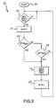
- FIG. 3is a flow chart showing a process for controlling the number of posted write requests that have been accumulated in a posted write buffer in the memory hub shown in FIG. 2 .
- FIG. 1A computer system 100 according to one example of the invention is shown in FIG. 1 .
- the computer system 100includes a processor 104 for performing various computing functions, such as executing specific software to perform specific calculations or tasks.
- the processor 104includes a processor bus 106 that normally includes an address bus, a control bus, and a data bus.
- the processor bus 106is typically coupled to cache memory 108 , which, as previously mentioned, is usually static random access memory (“SRAM”).
- SRAMstatic random access memory
- the processor bus 106is coupled to a system controller 110 , which is also sometimes referred to as a “North Bridge” or “memory controller.”
- the system controller 110serves as a communications path to the processor 104 for a variety of other components. More specifically, the system controller 110 includes a graphics port that is typically coupled to a graphics controller 112 , which is, in turn, coupled to a video terminal 114 . The system controller 110 is also coupled to one or more input devices 118 , such as a keyboard or a mouse, to allow an operator to interface with the computer system 100 . Typically, the computer system 100 also includes one or more output devices 120 , such as a printer, coupled to the processor 104 through the system controller 110 . One or more data storage devices 124 are also typically coupled to the processor 104 through the system controller 110 to allow the processor 104 to store data or retrieve data from internal or external storage media (not shown). Examples of typical storage devices 124 include hard and floppy disks, tape cassettes, and compact disk read-only memories (CD-ROMs).
- CD-ROMscompact disk read-only memories
- the system controller 110is coupled to several memory modules 130 a,b . . . n , which serve as system memory for the computer system 100 .
- the memory modules 130are preferably coupled to the system controller 110 through a high-speed link 134 , which may be an optical or electrical communication path or some other type of communications path.
- the high-speed link 134is implemented as an optical communication path, the optical communication path may be in the form of one or more optical fibers, for example.
- the system controller 110 and the memory moduleswill include an optical input/output port or separate input and output ports coupled to the optical communication path.
- the memory modules 130are shown coupled to the system controller 110 in a multi-drop arrangement in which the single high-speed link 134 is coupled to all of the memory modules 130 .
- topologiessuch as a point-to-point coupling arrangement in which a separate high-speed link (not shown) is used to couple each of the memory modules 130 to the system controller 110 .
- a switching topologymay also be used in which the system controller 110 is selectively coupled to each of the memory modules 130 through a switch (not shown).
- Other topologies that may be usedwill be apparent to one skilled in the art.
- Each of the memory modules 130includes a memory hub 140 for controlling access to 6 memory devices 148 , which, in the example illustrated in FIG. 2 , are synchronous dynamic random access memory (“SDRAM”) devices. However, a fewer or greater number of memory devices 148 may be used, and memory devices other than SDRAM devices may, of course, also be used.
- the memory hub 140is coupled to each of the system memory devices 148 through a bus system 150 , which normally includes a control bus, an address bus and a data bus.
- the memory hub 140 of FIG. 1includes a link interface 152 that is coupled to the high-speed link 134 .
- the nature of the link interface 152will depend upon the characteristics of the high-speed link 134 .
- the link interface 152will include an optical input/output port or separate input and output ports and will convert optical signals received through the optical communications path into electrical signals and electrical signals into optical signals that are transmitted to the optical communications path.
- the link interface 152may include a variety of conventional interface circuitry such as, for example, a first-in, first-out buffer (not shown), for receiving and storing memory requests as they are received through the high-speed link 134 .
- the memory requestscan then be stored in the link interface until they can be processed by the memory hub 140 .
- a memory request received by the link interface 152is processed by first transferring the request to a posted write buffer 160 . If the memory request is a write request, the request will be stored for subsequent processing, as explained in greater detail below. If the memory request is a read request, conventional coherency circuitry 162 in the posted write buffer 160 checks to determine if the read request is to an address to which a previous write request still stored in the buffer is directed. For example, the coherency circuitry can 162 post write request addresses to a posted address buffer. The address forming part of each read request can then be compared to the addresses in the posted address buffer.
- the read data called for by the read requestare returned from the posted write buffer 160 .
- the posted write dataare coupled from the posted write buffer 160 to one port of a multiplexer 164 .
- the coherency circuitry 162 in the posted write buffer 160also applies a control signal to the multiplexer 164 to couple the posted write data to the link interface 152 .
- the posted write buffer 160applies an active high MISS signal to a memory sequencer 170 , which receives the read request from the link interface 152 as “Read Around Write” request.
- the memory sequencer 170responds to the MISS signal by placing the read request in the proper sequence with other read requests and subsequently coupling the read request to a memory device interface 174 .
- the memory sequencer 170may also convert the read requests from the format output from the system controller 110 ( FIG. 1 ) into a read request having a format that can be used by the memory devices 148 .
- These reformatted request signalswill normally include memory command signals, which are derived from memory commands contained in the memory request received by the memory hub 140 , and row and column address signals, which are derived from an address contained in the memory request received by the memory hub 140 .
- the memory sequencer 170will output row address signals, a row address strobe (“RAS”) signal, an active low write/active low read signal (“W/R*”), column address signals and a column address strobe (“CAS”) signal.
- RASrow address strobe
- W/R*active low write/active low read signal
- CAScolumn address strobe
- the re-formatted memory requestsare preferably output from the memory sequencer 170 in the order they will be used by the memory devices 148 .
- the memory devices 148After the memory device interface 174 has applied the read request to the memory devices 148 , the memory devices 148 return read data called for by the request to the memory device interface 174 .
- the memory device interface 174then couples the read data to the other input port of the multiplexer 164 . If the posted write buffer 160 outputs an inactive low MISS signal, it also couples a control signal to the multiplexer 164 that causes the read data from the memory device interface 174 to be coupled to the link interface 152 .
- the link interface 152then couples the read data to the controller 110 through the high-speed link 134 .
- the coherency circuit 162may instead cause the read request to be delayed and immediately issue the posted write request to write data to the memory devices 148 .
- the memory hub 140can then issue the read request to the memory devices 148 to read the data that has now been written to the memory devices 148 at the memory read address.
- Other means of ensuring coherencythat may be used in the event a read request is serviced before servicing a write request to the same address will be apparent to one skilled in the art.
- the memory sequencer 170applies the read around write memory requests to the memory device interface 174 .
- the nature of the memory device interface 174will again depend upon the characteristics of the memory devices 148 .
- the memory device interface 174may include a FIFO buffer (not shown), for receiving and storing one or more memory requests as they are received from the link interface 152 .
- the memory requestcan be stored in the FIFO buffer until they can be processed by the memory devices 148 .
- the memory device interface 174can simply pass the memory requests to the memory devices 148 .
- the memory device interface 174may re-order the memory requests so that they are applied to the memory devices 148 in some other order.
- write requests posted in the buffer 160will accumulate to a level that they must be serviced.
- Various techniques for controlling the level of posted write requests that can accumulatewill be discussed below.
- the posted write buffer 160couples the write requests to the memory device interface 174 .
- These write requestswill normally include the write data as well as the address to which that data are to be written and appropriate command signals, as are well known to one skilled in the art.
- the memory device interface 174then passes the write requests on to the memory device 148 addressed by the write request.
- the accumulation of posted write requests in the buffer 160may be controlled by the process 200 shown in FIG. 3 .
- the process 200is entered at 202 and waits at 206 for a new write request to be received from the link interface 152 .
- a counter keeping track of the number W of posted write requests accumulated in the posted write buffer 160is incremented at 210 .
- the processthen checks at 214 to determine if the number of posted write requests W accumulated exceeds a maximum number, W MAX . If W exceeds W MAX , the posted write buffer 160 couples a write request to the memory device interface 174 at 218 .
- the posted write buffer 160can issue the write requests in any desired order, such as on a first-in, first-out order, a first-in, last-out order or some or other order, as is well known to one skilled in the art. In any case, once the posted write buffer 160 has issued the write request, the number of of posted write requests W accumulated is decremented by one at 220 . The process then returns to 206 to await another write request.
- the posted write buffer 160will issue write requests only when W MAX write requests have been accumulated in the buffer 160 until the number of write requests posted in the buffer 160 falls to some predetermined number which may be zero. Under these circumstances, the posted write buffer 160 would never issue the final W MAX write requests. For this reason, if the process 200 determines at 214 that W does not exceed W MAX , the process 200 checks at 226 to determine if the time T W any write request has remained in the posted write buffer 160 exceeds a maximum time T MAX . If so, the process 200 branches to 218 to issue the overdue write requests, as previously explained. Otherwise, the process returns to 206 to await a new write request.
- posted write requestscould be issued by the buffer 160 after they had remained there for a predetermined period of time regardless of how many write requests had been accumulated.
- the posted write buffer 160can also issue the posted write requests whenever read requests are not being processed by the memory hub 140 or the memory devices 148 coupled thereto.
- the values W MAX and T MAXmay be adjusted depending on various operating conditions. For example, the maximum number of posted write requests accumulated W MAX could be adjusted depending upon the rate at which posted write requests are being accumulated. Other variations will be apparent to one skilled in the art.
Landscapes
- Engineering & Computer Science (AREA)
- Microelectronics & Electronic Packaging (AREA)
- Computer Hardware Design (AREA)
- Databases & Information Systems (AREA)
- Memory System Of A Hierarchy Structure (AREA)
Abstract
Description
Claims (14)
Priority Applications (2)
| Application Number | Priority Date | Filing Date | Title |
|---|---|---|---|
| US10/601,253US7107415B2 (en) | 2003-06-20 | 2003-06-20 | Posted write buffers and methods of posting write requests in memory modules |
| US11/433,201US7529896B2 (en) | 2003-06-20 | 2006-05-11 | Memory modules having a memory hub containing a posted write buffer, a memory device interface and a link interface, and method of posting write requests in memory modules |
Applications Claiming Priority (1)
| Application Number | Priority Date | Filing Date | Title |
|---|---|---|---|
| US10/601,253US7107415B2 (en) | 2003-06-20 | 2003-06-20 | Posted write buffers and methods of posting write requests in memory modules |
Related Child Applications (1)
| Application Number | Title | Priority Date | Filing Date |
|---|---|---|---|
| US11/433,201ContinuationUS7529896B2 (en) | 2003-06-20 | 2006-05-11 | Memory modules having a memory hub containing a posted write buffer, a memory device interface and a link interface, and method of posting write requests in memory modules |
Publications (2)
| Publication Number | Publication Date |
|---|---|
| US20040260891A1 US20040260891A1 (en) | 2004-12-23 |
| US7107415B2true US7107415B2 (en) | 2006-09-12 |
Family
ID=33517935
Family Applications (2)
| Application Number | Title | Priority Date | Filing Date |
|---|---|---|---|
| US10/601,253Expired - Fee RelatedUS7107415B2 (en) | 2003-06-20 | 2003-06-20 | Posted write buffers and methods of posting write requests in memory modules |
| US11/433,201Expired - Fee RelatedUS7529896B2 (en) | 2003-06-20 | 2006-05-11 | Memory modules having a memory hub containing a posted write buffer, a memory device interface and a link interface, and method of posting write requests in memory modules |
Family Applications After (1)
| Application Number | Title | Priority Date | Filing Date |
|---|---|---|---|
| US11/433,201Expired - Fee RelatedUS7529896B2 (en) | 2003-06-20 | 2006-05-11 | Memory modules having a memory hub containing a posted write buffer, a memory device interface and a link interface, and method of posting write requests in memory modules |
Country Status (1)
| Country | Link |
|---|---|
| US (2) | US7107415B2 (en) |
Cited By (16)
| Publication number | Priority date | Publication date | Assignee | Title |
|---|---|---|---|---|
| US20060106980A1 (en)* | 2004-11-12 | 2006-05-18 | Hitachi Global Storage Technologies Netherlands B.V. | Media drive and command execution method thereof |
| US20070162659A1 (en)* | 2004-04-01 | 2007-07-12 | Nvidia Corporation | Deadlock Avoidance in a Bus Fabric |
| US7353320B2 (en) | 2004-05-14 | 2008-04-01 | Micron Technology, Inc. | Memory hub and method for memory sequencing |
| US7412566B2 (en) | 2003-06-20 | 2008-08-12 | Micron Technology, Inc. | Memory hub and access method having internal prefetch buffers |
| US7434081B2 (en) | 2003-12-29 | 2008-10-07 | Micron Technology, Inc. | System and method for read synchronization of memory modules |
| US20090150624A1 (en)* | 2007-11-15 | 2009-06-11 | Micron Technology, Inc. | System, apparatus, and method for modifying the order of memory accesseses |
| US7644253B2 (en) | 2002-06-07 | 2010-01-05 | Micron Technology, Inc. | Memory hub with internal cache and/or memory access prediction |
| US7716444B2 (en) | 2002-08-29 | 2010-05-11 | Round Rock Research, Llc | Method and system for controlling memory accesses to memory modules having a memory hub architecture |
| US20100250874A1 (en)* | 2009-03-24 | 2010-09-30 | Farrell Todd D | Apparatus and method for buffered write commands in a memory |
| US7818712B2 (en) | 2003-06-19 | 2010-10-19 | Round Rock Research, Llc | Reconfigurable memory module and method |
| US8239607B2 (en) | 2004-06-04 | 2012-08-07 | Micron Technology, Inc. | System and method for an asynchronous data buffer having buffer write and read pointers |
| US8504782B2 (en) | 2004-01-30 | 2013-08-06 | Micron Technology, Inc. | Buffer control system and method for a memory system having outstanding read and write request buffers |
| US8589643B2 (en) | 2003-10-20 | 2013-11-19 | Round Rock Research, Llc | Arbitration system and method for memory responses in a hub-based memory system |
| US8588017B2 (en) | 2010-10-20 | 2013-11-19 | Samsung Electronics Co., Ltd. | Memory circuits, systems, and modules for performing DRAM refresh operations and methods of operating the same |
| US8954687B2 (en) | 2002-08-05 | 2015-02-10 | Micron Technology, Inc. | Memory hub and access method having a sequencer and internal row caching |
| US10679722B2 (en) | 2016-08-26 | 2020-06-09 | Sandisk Technologies Llc | Storage system with several integrated components and method for use therewith |
Families Citing this family (19)
| Publication number | Priority date | Publication date | Assignee | Title |
|---|---|---|---|---|
| US6791555B1 (en) | 2000-06-23 | 2004-09-14 | Micron Technology, Inc. | Apparatus and method for distributed memory control in a graphics processing system |
| US7133991B2 (en)* | 2003-08-20 | 2006-11-07 | Micron Technology, Inc. | Method and system for capturing and bypassing memory transactions in a hub-based memory system |
| US20050138281A1 (en)* | 2003-12-18 | 2005-06-23 | Garney John I. | Request processing order in a cache |
| US7213082B2 (en) | 2004-03-29 | 2007-05-01 | Micron Technology, Inc. | Memory hub and method for providing memory sequencing hints |
| US7213095B2 (en)* | 2004-06-08 | 2007-05-01 | Arm Limited | Bus transaction management within data processing systems |
| US20060230455A1 (en)* | 2005-04-12 | 2006-10-12 | Yuan-Chang Lo | Apparatus and methods for file system with write buffer to protect against malware |
| US8082396B2 (en)* | 2005-04-28 | 2011-12-20 | International Business Machines Corporation | Selecting a command to send to memory |
| US20070079057A1 (en)* | 2005-09-30 | 2007-04-05 | Hermann Ruckerbauer | Semiconductor memory system and memory module |
| US8341360B2 (en) | 2005-12-30 | 2012-12-25 | Intel Corporation | Method and apparatus for memory write performance optimization in architectures with out-of-order read/request-for-ownership response |
| US7487284B2 (en)* | 2006-07-28 | 2009-02-03 | Intel Corporation | Transaction flow and ordering for a packet processing engine, located within an input-output hub |
| US10776489B2 (en) | 2007-03-06 | 2020-09-15 | Unisys Corporation | Methods and systems for providing and controlling cryptographic secure communications terminal operable to provide a plurality of desktop environments |
| US20110004718A1 (en)* | 2009-07-02 | 2011-01-06 | Ross John Stenfort | System, method, and computer program product for ordering a plurality of write commands associated with a storage device |
| US8838853B2 (en)* | 2010-01-18 | 2014-09-16 | Marvell International Ltd. | Access buffer |
| WO2011149482A1 (en) | 2010-05-28 | 2011-12-01 | Hewlett-Packard Development Company, L.P. | Storing data in any of a plurality of buffers in a memory controller |
| US11030305B2 (en) | 2010-10-04 | 2021-06-08 | Unisys Corporation | Virtual relay device for providing a secure connection to a remote device |
| US9702305B2 (en)* | 2013-04-17 | 2017-07-11 | Micron Technology, Inc. | Multiple engine sequencer |
| WO2015170550A1 (en)* | 2014-05-09 | 2015-11-12 | ソニー株式会社 | Memory control device, memory device, and memory control method for same |
| US20170308296A1 (en)* | 2016-04-22 | 2017-10-26 | Hewlett Packard Enterprise Development Lp | Staging write requests |
| US10789001B1 (en)* | 2016-11-21 | 2020-09-29 | Innovium, Inc. | Posted operation data control |
Citations (218)
| Publication number | Priority date | Publication date | Assignee | Title |
|---|---|---|---|---|
| US3742253A (en) | 1971-03-15 | 1973-06-26 | Burroughs Corp | Three state logic device with applications |
| US4045781A (en) | 1976-02-13 | 1977-08-30 | Digital Equipment Corporation | Memory module with selectable byte addressing for digital data processing system |
| US4240143A (en) | 1978-12-22 | 1980-12-16 | Burroughs Corporation | Hierarchical multi-processor network for memory sharing |
| US4245306A (en) | 1978-12-21 | 1981-01-13 | Burroughs Corporation | Selection of addressed processor in a multi-processor network |
| US4253144A (en) | 1978-12-21 | 1981-02-24 | Burroughs Corporation | Multi-processor communication network |
| US4253146A (en) | 1978-12-21 | 1981-02-24 | Burroughs Corporation | Module for coupling computer-processors |
| US4707823A (en) | 1986-07-21 | 1987-11-17 | Chrysler Motors Corporation | Fiber optic multiplexed data acquisition system |
| US4724520A (en) | 1985-07-01 | 1988-02-09 | United Technologies Corporation | Modular multiport data hub |
| US4831520A (en) | 1987-02-24 | 1989-05-16 | Digital Equipment Corporation | Bus interface circuit for digital data processor |
| US4930128A (en) | 1987-06-26 | 1990-05-29 | Hitachi, Ltd. | Method for restart of online computer system and apparatus for carrying out the same |
| US4953930A (en) | 1989-03-15 | 1990-09-04 | Ramtech, Inc. | CPU socket supporting socket-to-socket optical communications |
| US5241506A (en) | 1989-11-15 | 1993-08-31 | Kabushiki Kaisha Toshiba | Semiconductor memory circuit apparatus |
| US5243703A (en) | 1990-04-18 | 1993-09-07 | Rambus, Inc. | Apparatus for synchronously generating clock signals in a data processing system |
| WO1993019422A1 (en) | 1992-03-25 | 1993-09-30 | Encore Computer U.S., Inc. | Fiber optic memory coupling system |
| US5251303A (en) | 1989-01-13 | 1993-10-05 | International Business Machines Corporation | System for DMA block data transfer based on linked control blocks |
| US5269022A (en) | 1990-03-28 | 1993-12-07 | Kabushiki Kaisha Toshiba | Method and apparatus for booting a computer system by restoring the main memory from a backup memory |
| US5313590A (en) | 1990-01-05 | 1994-05-17 | Maspar Computer Corporation | System having fixedly priorized and grouped by positions I/O lines for interconnecting router elements in plurality of stages within parrallel computer |
| US5317752A (en) | 1989-12-22 | 1994-05-31 | Tandem Computers Incorporated | Fault-tolerant computer system with auto-restart after power-fall |
| US5319755A (en) | 1990-04-18 | 1994-06-07 | Rambus, Inc. | Integrated circuit I/O using high performance bus interface |
| US5355391A (en) | 1992-03-06 | 1994-10-11 | Rambus, Inc. | High speed bus system |
| US5432907A (en) | 1992-05-12 | 1995-07-11 | Network Resources Corporation | Network hub with integrated bridge |
| US5432823A (en) | 1992-03-06 | 1995-07-11 | Rambus, Inc. | Method and circuitry for minimizing clock-data skew in a bus system |
| US5442770A (en) | 1989-01-24 | 1995-08-15 | Nec Electronics, Inc. | Triple port cache memory |
| US5461627A (en) | 1991-12-24 | 1995-10-24 | Rypinski; Chandos A. | Access protocol for a common channel wireless network |
| US5465229A (en) | 1992-05-19 | 1995-11-07 | Sun Microsystems, Inc. | Single in-line memory module |
| US5479370A (en) | 1992-02-20 | 1995-12-26 | Kabushiki Kaisha Toshiba | Semiconductor memory with bypass circuit |
| US5497476A (en) | 1992-09-21 | 1996-03-05 | International Business Machines Corporation | Scatter-gather in data processing system |
| US5502621A (en) | 1994-03-31 | 1996-03-26 | Hewlett-Packard Company | Mirrored pin assignment for two sided multi-chip layout |
| US5566325A (en) | 1994-06-30 | 1996-10-15 | Digital Equipment Corporation | Method and apparatus for adaptive memory access |
| US5577220A (en) | 1993-07-23 | 1996-11-19 | International Business Machines Corporation | Method for saving and restoring the state of a CPU executing code in protected mode including estimating the value of the page table base register |
| US5581767A (en) | 1993-06-16 | 1996-12-03 | Nippon Sheet Glass Co., Ltd. | Bus structure for multiprocessor system having separated processor section and control/memory section |
| US5638534A (en)* | 1995-03-31 | 1997-06-10 | Samsung Electronics Co., Ltd. | Memory controller which executes read and write commands out of order |
| US5659798A (en) | 1996-02-02 | 1997-08-19 | Blumrich; Matthias Augustin | Method and system for initiating and loading DMA controller registers by using user-level programs |
| US5687325A (en) | 1996-04-19 | 1997-11-11 | Chang; Web | Application specific field programmable gate array |
| US5706224A (en) | 1996-10-10 | 1998-01-06 | Quality Semiconductor, Inc. | Content addressable memory and random access memory partition circuit |
| US5710733A (en) | 1996-01-22 | 1998-01-20 | Silicon Graphics, Inc. | Processor-inclusive memory module |
| US5715456A (en) | 1995-02-13 | 1998-02-03 | International Business Machines Corporation | Method and apparatus for booting a computer system without pre-installing an operating system |
| US5729709A (en) | 1993-11-12 | 1998-03-17 | Intel Corporation | Memory controller with burst addressing circuit |
| EP0849685A2 (en) | 1996-12-19 | 1998-06-24 | Texas Instruments Incorporated | Communication bus system between processors and memory modules |
| US5796413A (en)* | 1995-12-06 | 1998-08-18 | Compaq Computer Corporation | Graphics controller utilizing video memory to provide macro command capability and enhanched command buffering |
| US5819304A (en) | 1996-01-29 | 1998-10-06 | Iowa State University Research Foundation, Inc. | Random access memory assembly |
| US5818844A (en) | 1996-06-06 | 1998-10-06 | Advanced Micro Devices, Inc. | Address generation and data path arbitration to and from SRAM to accommodate multiple transmitted packets |
| US5822255A (en) | 1996-08-13 | 1998-10-13 | Fujitsu Limited | Semiconductor integrated circuit for supplying a control signal to a plurality of object circuits |
| US5832250A (en) | 1996-01-26 | 1998-11-03 | Unisys Corporation | Multi set cache structure having parity RAMs holding parity bits for tag data and for status data utilizing prediction circuitry that predicts and generates the needed parity bits |
| US5875352A (en) | 1995-11-03 | 1999-02-23 | Sun Microsystems, Inc. | Method and apparatus for multiple channel direct memory access control |
| US5875454A (en) | 1996-07-24 | 1999-02-23 | International Business Machiness Corporation | Compressed data cache storage system |
| US5887159A (en) | 1996-12-11 | 1999-03-23 | Digital Equipment Corporation | Dynamically determining instruction hint fields |
| US5966724A (en) | 1996-01-11 | 1999-10-12 | Micron Technology, Inc. | Synchronous memory device with dual page and burst mode operations |
| US5973935A (en) | 1997-04-07 | 1999-10-26 | Micron Technology, Inc. | Interdigitated leads-over-chip lead frame for supporting an integrated circuit die |
| US5978567A (en) | 1994-07-27 | 1999-11-02 | Instant Video Technologies Inc. | System for distribution of interactive multimedia and linear programs by enabling program webs which include control scripts to define presentation by client transceiver |
| US5987196A (en) | 1997-11-06 | 1999-11-16 | Micron Technology, Inc. | Semiconductor structure having an optical signal path in a substrate and method for forming the same |
| US6011741A (en) | 1991-04-11 | 2000-01-04 | Sandisk Corporation | Computer memory cards using flash EEPROM integrated circuit chips and memory-controller systems |
| US6023726A (en) | 1998-01-20 | 2000-02-08 | Netscape Communications Corporation | User configurable prefetch control system for enabling client to prefetch documents from a network server |
| US6029250A (en) | 1998-09-09 | 2000-02-22 | Micron Technology, Inc. | Method and apparatus for adaptively adjusting the timing offset between a clock signal and digital signals transmitted coincident with that clock signal, and memory device and system using same |
| US6031241A (en) | 1997-03-11 | 2000-02-29 | University Of Central Florida | Capillary discharge extreme ultraviolet lamp source for EUV microlithography and other related applications |
| US6033951A (en) | 1996-08-16 | 2000-03-07 | United Microelectronics Corp. | Process for fabricating a storage capacitor for semiconductor memory devices |
| US6038630A (en) | 1998-03-24 | 2000-03-14 | International Business Machines Corporation | Shared access control device for integrated system with multiple functional units accessing external structures over multiple data buses |
| US6061263A (en) | 1998-12-29 | 2000-05-09 | Intel Corporation | Small outline rambus in-line memory module |
| US6061296A (en) | 1998-08-17 | 2000-05-09 | Vanguard International Semiconductor Corporation | Multiple data clock activation with programmable delay for use in multiple CAS latency memory devices |
| US6067649A (en) | 1998-06-10 | 2000-05-23 | Compaq Computer Corporation | Method and apparatus for a low power self test of a memory subsystem |
| US6067262A (en) | 1998-12-11 | 2000-05-23 | Lsi Logic Corporation | Redundancy analysis for embedded memories with built-in self test and built-in self repair |
| US6073190A (en) | 1997-07-18 | 2000-06-06 | Micron Electronics, Inc. | System for dynamic buffer allocation comprising control logic for controlling a first address buffer and a first data buffer as a matched pair |
| US6076139A (en) | 1996-12-31 | 2000-06-13 | Compaq Computer Corporation | Multimedia computer architecture with multi-channel concurrent memory access |
| US6079008A (en) | 1998-04-03 | 2000-06-20 | Patton Electronics Co. | Multiple thread multiple data predictive coded parallel processing system and method |
| US6092158A (en)* | 1997-06-13 | 2000-07-18 | Intel Corporation | Method and apparatus for arbitrating between command streams |
| US6098158A (en) | 1997-12-18 | 2000-08-01 | International Business Machines Corporation | Software-enabled fast boot |
| US6105075A (en) | 1997-08-05 | 2000-08-15 | Adaptec, Inc. | Scatter gather memory system for a hardware accelerated command interpreter engine |
| US6125431A (en) | 1996-08-02 | 2000-09-26 | Oki Electric Industry Co., Ltd. | Single-chip microcomputer using adjustable timing to fetch data from an external memory |
| US6128703A (en) | 1997-09-05 | 2000-10-03 | Integrated Device Technology, Inc. | Method and apparatus for memory prefetch operation of volatile non-coherent data |
| US6134624A (en) | 1998-06-08 | 2000-10-17 | Storage Technology Corporation | High bandwidth cache system |
| US6144587A (en) | 1998-06-23 | 2000-11-07 | Nec Corporation | Semiconductor memory device |
| US6145033A (en) | 1998-07-17 | 2000-11-07 | Seiko Epson Corporation | Management of display FIFO requests for DRAM access wherein low priority requests are initiated when FIFO level is below/equal to high threshold value |
| US6167486A (en) | 1996-11-18 | 2000-12-26 | Nec Electronics, Inc. | Parallel access virtual channel memory system with cacheable channels |
| US6167465A (en) | 1998-05-20 | 2000-12-26 | Aureal Semiconductor, Inc. | System for managing multiple DMA connections between a peripheral device and a memory and performing real-time operations on data carried by a selected DMA connection |
| US6175571B1 (en) | 1994-07-22 | 2001-01-16 | Network Peripherals, Inc. | Distributed memory switching hub |
| US6185352B1 (en) | 2000-02-24 | 2001-02-06 | Siecor Operations, Llc | Optical fiber ribbon fan-out cables |
| US6185676B1 (en) | 1997-09-30 | 2001-02-06 | Intel Corporation | Method and apparatus for performing early branch prediction in a microprocessor |
| US6186400B1 (en) | 1998-03-20 | 2001-02-13 | Symbol Technologies, Inc. | Bar code reader with an integrated scanning component module mountable on printed circuit board |
| US6191663B1 (en) | 1998-12-22 | 2001-02-20 | Intel Corporation | Echo reduction on bit-serial, multi-drop bus |
| US6201724B1 (en) | 1998-11-12 | 2001-03-13 | Nec Corporation | Semiconductor memory having improved register array access speed |
| US6212590B1 (en) | 1997-12-22 | 2001-04-03 | Compaq Computer Corporation | Computer system having integrated bus bridge design with delayed transaction arbitration mechanism employed within laptop computer docked to expansion base |
| US6223301B1 (en)* | 1997-09-30 | 2001-04-24 | Compaq Computer Corporation | Fault tolerant memory |
| US6233376B1 (en) | 1999-05-18 | 2001-05-15 | The United States Of America As Represented By The Secretary Of The Navy | Embedded fiber optic circuit boards and integrated circuits |
| US6243831B1 (en) | 1998-10-31 | 2001-06-05 | Compaq Computer Corporation | Computer system with power loss protection mechanism |
| US6243769B1 (en) | 1997-07-18 | 2001-06-05 | Micron Technology, Inc. | Dynamic buffer allocation for a computer system |
| US6247107B1 (en) | 1998-04-06 | 2001-06-12 | Advanced Micro Devices, Inc. | Chipset configured to perform data-directed prefetching |
| US6246618B1 (en) | 2000-06-30 | 2001-06-12 | Mitsubishi Denki Kabushiki Kaisha | Semiconductor integrated circuit capable of testing and substituting defective memories and method thereof |
| US6249802B1 (en) | 1997-09-19 | 2001-06-19 | Silicon Graphics, Inc. | Method, system, and computer program product for allocating physical memory in a distributed shared memory network |
| US6256692B1 (en) | 1997-10-13 | 2001-07-03 | Fujitsu Limited | CardBus interface circuit, and a CardBus PC having the same |
| US6272609B1 (en) | 1998-07-31 | 2001-08-07 | Micron Electronics, Inc. | Pipelined memory controller |
| US6286083B1 (en) | 1998-07-08 | 2001-09-04 | Compaq Computer Corporation | Computer system with adaptive memory arbitration scheme |
| US6285349B1 (en) | 1999-02-26 | 2001-09-04 | Intel Corporation | Correcting non-uniformity in displays |
| US6294937B1 (en) | 1999-05-25 | 2001-09-25 | Lsi Logic Corporation | Method and apparatus for self correcting parallel I/O circuitry |
| JP2001265539A (en) | 2000-03-16 | 2001-09-28 | Fuji Xerox Co Ltd | Array type storage device and information processing system |
| US6301637B1 (en) | 1998-06-08 | 2001-10-09 | Storage Technology Corporation | High performance data paths |
| US20010039612A1 (en) | 1999-12-02 | 2001-11-08 | Lee Sang-Jin | Apparatus and method for fast booting |
| US6330205B2 (en) | 1999-12-22 | 2001-12-11 | Nec Corporation | Virtual channel synchronous dynamic random access memory |
| US6347055B1 (en) | 1999-06-24 | 2002-02-12 | Nec Corporation | Line buffer type semiconductor memory device capable of direct prefetch and restore operations |
| US6349363B2 (en) | 1998-12-08 | 2002-02-19 | Intel Corporation | Multi-section cache with different attributes for each section |
| US6356573B1 (en) | 1998-01-31 | 2002-03-12 | Mitel Semiconductor Ab | Vertical cavity surface emitting laser |
| US6367074B1 (en) | 1998-12-28 | 2002-04-02 | Intel Corporation | Operation of a system |
| WO2002027499A2 (en) | 2000-09-29 | 2002-04-04 | Intel Corporation | Shared translation address caching |
| US6370068B2 (en) | 2000-01-05 | 2002-04-09 | Samsung Electronics Co., Ltd. | Semiconductor memory devices and methods for sampling data therefrom based on a relative position of a memory cell array section containing the data |
| US6370611B1 (en)* | 2000-04-04 | 2002-04-09 | Compaq Computer Corporation | Raid XOR operations to synchronous DRAM using a read buffer and pipelining of synchronous DRAM burst read data |
| US20020042863A1 (en)* | 1999-07-29 | 2002-04-11 | Joseph M. Jeddeloh | Storing a flushed cache line in a memory buffer of a controller |
| US6373777B1 (en) | 1998-07-14 | 2002-04-16 | Nec Corporation | Semiconductor memory |
| US6381190B1 (en) | 1999-05-13 | 2002-04-30 | Nec Corporation | Semiconductor memory device in which use of cache can be selected |
| US6389514B1 (en) | 1999-03-25 | 2002-05-14 | Hewlett-Packard Company | Method and computer system for speculatively closing pages in memory |
| US6392653B1 (en) | 1998-06-25 | 2002-05-21 | Inria Institut National De Recherche En Informatique Et En Automatique | Device for processing acquisition data, in particular image data |
| US6401213B1 (en) | 1999-07-09 | 2002-06-04 | Micron Technology, Inc. | Timing circuit for high speed memory |
| US6405280B1 (en) | 1998-06-05 | 2002-06-11 | Micron Technology, Inc. | Packet-oriented synchronous DRAM interface supporting a plurality of orderings for data block transfers within a burst sequence |
| US6421744B1 (en) | 1999-10-25 | 2002-07-16 | Motorola, Inc. | Direct memory access controller and method therefor |
| US6430696B1 (en) | 1998-11-30 | 2002-08-06 | Micron Technology, Inc. | Method and apparatus for high speed data capture utilizing bit-to-bit timing correction, and memory device using same |
| US6434736B1 (en) | 1999-07-08 | 2002-08-13 | Intel Corporation | Location based timing scheme in memory design |
| US6434639B1 (en) | 1998-11-13 | 2002-08-13 | Intel Corporation | System for combining requests associated with one or more memory locations that are collectively associated with a single cache line to furnish a single memory operation |
| US6433785B1 (en)* | 1999-04-09 | 2002-08-13 | Intel Corporation | Method and apparatus for improving processor to graphics device throughput |
| US6434696B1 (en) | 1998-05-11 | 2002-08-13 | Lg Electronics Inc. | Method for quickly booting a computer system |
| US20020112119A1 (en) | 1998-02-13 | 2002-08-15 | Intel Corporation | Dual-port buffer-to-memory interface |
| US6438622B1 (en) | 1998-11-17 | 2002-08-20 | Intel Corporation | Multiprocessor system including a docking system |
| US6438668B1 (en) | 1999-09-30 | 2002-08-20 | Apple Computer, Inc. | Method and apparatus for reducing power consumption in a digital processing system |
| US20020116588A1 (en) | 2000-12-20 | 2002-08-22 | Beckert Richard Dennis | Software management systems and methods for automotive computing devices |
| US6449308B1 (en) | 1999-05-25 | 2002-09-10 | Intel Corporation | High-speed digital distribution system |
| US6453393B1 (en) | 2000-09-18 | 2002-09-17 | Intel Corporation | Method and apparatus for interfacing to a computer memory |
| US6457116B1 (en) | 1997-10-31 | 2002-09-24 | Broadcom Corporation | Method and apparatus for controlling contexts of multiple context processing elements in a network of multiple context processing elements |
| US6460108B1 (en) | 1999-03-31 | 2002-10-01 | Intel Corporation | Low cost data streaming mechanism |
| US20020144064A1 (en) | 2001-03-30 | 2002-10-03 | Fanning Blaise B. | Controlling cache memory in external chipset using processor |
| US6462978B2 (en) | 1997-08-21 | 2002-10-08 | Hitachi, Ltd. | Method of designing semiconductor integrated circuit device and semiconductor integrated circuit device |
| US6463059B1 (en) | 1998-12-04 | 2002-10-08 | Koninklijke Philips Electronics N.V. | Direct memory access execution engine with indirect addressing of circular queues in addition to direct memory addressing |
| US6473828B1 (en) | 1998-07-03 | 2002-10-29 | Nec Corporation | Virtual channel synchronous dynamic random access memory |
| US6477614B1 (en) | 1998-09-30 | 2002-11-05 | Intel Corporation | Method for implementing multiple memory buses on a memory module |
| US6477592B1 (en) | 1999-08-06 | 2002-11-05 | Integrated Memory Logic, Inc. | System for I/O interfacing for semiconductor chip utilizing addition of reference element to each data element in first data stream and interpret to recover data elements of second data stream |
| US6479322B2 (en) | 1998-06-01 | 2002-11-12 | Hitachi, Ltd. | Semiconductor device with two stacked chips in one resin body and method of producing |
| US6487556B1 (en) | 1998-12-18 | 2002-11-26 | International Business Machines Corporation | Method and system for providing an associative datastore within a data processing system |
| US20020178319A1 (en)* | 2001-05-24 | 2002-11-28 | Jorge Sanchez-Olea | Optical bus arrangement for computer system |
| US6490188B2 (en) | 1999-09-02 | 2002-12-03 | Micron Technology, Inc. | Semiconductor devices having mirrored terminal arrangements, devices including same, and methods of testing such semiconductor devices |
| US6496193B1 (en)* | 1999-12-30 | 2002-12-17 | Intel Corporation | Method and apparatus for fast loading of texture data into a tiled memory |
| US6496909B1 (en) | 1999-04-06 | 2002-12-17 | Silicon Graphics, Inc. | Method for managing concurrent access to virtual memory data structures |
| US6501471B1 (en) | 1999-12-13 | 2002-12-31 | Intel Corporation | Volume rendering |
| US20030005223A1 (en) | 2001-06-27 | 2003-01-02 | Coulson Richard L. | System boot time reduction method |
| US6505287B2 (en) | 1999-12-20 | 2003-01-07 | Nec Corporation | Virtual channel memory access controlling circuit |
| US6523092B1 (en) | 2000-09-29 | 2003-02-18 | Intel Corporation | Cache line replacement policy enhancement to avoid memory page thrashing |
| US6523093B1 (en) | 2000-09-29 | 2003-02-18 | Intel Corporation | Prefetch buffer allocation and filtering system |
| US6526498B1 (en) | 1997-10-31 | 2003-02-25 | Broadcom Corporation | Method and apparatus for retiming in a network of multiple context processing elements |
| US6526483B1 (en) | 2000-09-20 | 2003-02-25 | Broadcom Corporation | Page open hint in transactions |
| US20030043158A1 (en) | 2001-05-18 | 2003-03-06 | Wasserman Michael A. | Method and apparatus for reducing inefficiencies in shared memory devices |
| US20030043426A1 (en) | 2001-08-30 | 2003-03-06 | Baker R. J. | Optical interconnect in high-speed memory systems |
| US6539490B1 (en) | 1999-08-30 | 2003-03-25 | Micron Technology, Inc. | Clock distribution without clock delay or skew |
| US6552564B1 (en) | 1999-08-30 | 2003-04-22 | Micron Technology, Inc. | Technique to reduce reflections and ringing on CMOS interconnections |
| US20030093630A1 (en) | 2001-11-15 | 2003-05-15 | Richard Elizabeth A. | Techniques for processing out-of -order requests in a processor-based system |
| US6590816B2 (en) | 2001-03-05 | 2003-07-08 | Infineon Technologies Ag | Integrated memory and method for testing and repairing the integrated memory |
| US6594722B1 (en) | 2000-06-29 | 2003-07-15 | Intel Corporation | Mechanism for managing multiple out-of-order packet streams in a PCI host bridge |
| US6594713B1 (en) | 1999-09-10 | 2003-07-15 | Texas Instruments Incorporated | Hub interface unit and application unit interfaces for expanded direct memory access processor |
| US6598154B1 (en) | 1998-12-29 | 2003-07-22 | Intel Corporation | Precoding branch instructions to reduce branch-penalty in pipelined processors |
| US20030149809A1 (en) | 2001-08-29 | 2003-08-07 | Jensen Poul R. | Method and apparatus for timing and event processing in wireless systems |
| US20030163649A1 (en) | 2002-02-25 | 2003-08-28 | Kapur Suvansh K. | Shared bypass bus structure |
| US6615325B2 (en) | 1996-01-11 | 2003-09-02 | Micron Technology, Inc. | Method for switching between modes of operation |
| US6622227B2 (en) | 2000-12-27 | 2003-09-16 | Intel Corporation | Method and apparatus for utilizing write buffers in memory control/interface |
| US6629220B1 (en) | 1999-08-20 | 2003-09-30 | Intel Corporation | Method and apparatus for dynamic arbitration between a first queue and a second queue based on a high priority transaction type |
| US6628294B1 (en) | 1999-12-31 | 2003-09-30 | Intel Corporation | Prefetching of virtual-to-physical address translation for display data |
| US6631440B2 (en) | 2000-11-30 | 2003-10-07 | Hewlett-Packard Development Company | Method and apparatus for scheduling memory calibrations based on transactions |
| US20030193927A1 (en) | 2002-04-10 | 2003-10-16 | Stanley Hronik | Random access memory architecture and serial interface with continuous packet handling capability |
| US6636110B1 (en) | 1998-05-01 | 2003-10-21 | Mitsubishi Denki Kabushiki Kaisha | Internal clock generating circuit for clock synchronous semiconductor memory device |
| US6646929B1 (en) | 2001-12-05 | 2003-11-11 | Lsi Logic Corporation | Methods and structure for read data synchronization with minimal latency |
| US6647470B1 (en)* | 2000-08-21 | 2003-11-11 | Micron Technology, Inc. | Memory device having posted write per command |
| US6658509B1 (en) | 2000-10-03 | 2003-12-02 | Intel Corporation | Multi-tier point-to-point ring memory interface |
| US6662304B2 (en) | 1998-12-11 | 2003-12-09 | Micron Technology, Inc. | Method and apparatus for bit-to-bit timing correction of a high speed memory bus |
| US20030229762A1 (en) | 2002-06-11 | 2003-12-11 | Subramaniam Maiyuran | Apparatus, method, and system for synchronizing information prefetch between processors and memory controllers |
| US20030229770A1 (en)* | 2002-06-07 | 2003-12-11 | Jeddeloh Joseph M. | Memory hub with internal cache and/or memory access prediction |
| US6665202B2 (en) | 2001-09-25 | 2003-12-16 | Integrated Device Technology, Inc. | Content addressable memory (CAM) devices that can identify highest priority matches in non-sectored CAM arrays and methods of operating same |
| US6667895B2 (en) | 2001-12-06 | 2003-12-23 | Samsung Electronics Co., Ltd. | Integrated circuit device and module with integrated circuits |
| US6681292B2 (en) | 2001-08-27 | 2004-01-20 | Intel Corporation | Distributed read and write caching implementation for optimized input/output applications |
| US20040019728A1 (en)* | 2002-07-23 | 2004-01-29 | Sharma Debendra Das | Multiple hardware partitions under one input/output hub |
| US20040024978A1 (en)* | 2002-08-05 | 2004-02-05 | Jeddeloh Joseph M. | Memory hub and access method having internal row caching |
| US20040034753A1 (en)* | 2002-08-16 | 2004-02-19 | Jeddeloh Joseph M. | Memory hub bypass circuit and method |
| US20040034825A1 (en)* | 2002-08-16 | 2004-02-19 | Jeddeloh Joseph M. | System and method for self-testing and repair of memory modules |
| US6697926B2 (en) | 2001-06-06 | 2004-02-24 | Micron Technology, Inc. | Method and apparatus for determining actual write latency and accurately aligning the start of data capture with the arrival of data at a memory device |
| US20040044857A1 (en)* | 2002-08-29 | 2004-03-04 | Jeddeloh Joseph M. | Method and system for controlling memory accesses to memory modules having a memory hub architecture |
| US6704817B1 (en) | 2000-08-31 | 2004-03-09 | Hewlett-Packard Development Company, L.P. | Computer architecture and system for efficient management of bi-directional bus |
| US6715018B2 (en) | 1998-06-16 | 2004-03-30 | Micron Technology, Inc. | Computer including installable and removable cards, optical interconnection between cards, and method of assembling a computer |
| US20040064602A1 (en)* | 2002-09-30 | 2004-04-01 | Varghese George | Claiming cycles on a processor bus in a system having a PCI to PCI bridge north of a memory controller |
| US6718440B2 (en) | 2001-09-28 | 2004-04-06 | Intel Corporation | Memory access latency hiding with hint buffer |
| US6721195B2 (en) | 2001-07-12 | 2004-04-13 | Micron Technology, Inc. | Reversed memory module socket and motherboard incorporating same |
| US6724685B2 (en) | 2001-10-31 | 2004-04-20 | Infineon Technologies Ag | Configuration for data transmission in a semiconductor memory system, and relevant data transmission method |
| US6728800B1 (en) | 2000-06-28 | 2004-04-27 | Intel Corporation | Efficient performance based scheduling mechanism for handling multiple TLB operations |
| US6735682B2 (en) | 2002-03-28 | 2004-05-11 | Intel Corporation | Apparatus and method for address calculation |
| US6735679B1 (en) | 1998-07-08 | 2004-05-11 | Broadcom Corporation | Apparatus and method for optimizing access to memory |
| US6745275B2 (en) | 2000-01-25 | 2004-06-01 | Via Technologies, Inc. | Feedback system for accomodating different memory module loading |
| US6751703B2 (en) | 2000-12-27 | 2004-06-15 | Emc Corporation | Data storage systems and methods which utilize an on-board cache |
| US6754812B1 (en) | 2000-07-06 | 2004-06-22 | Intel Corporation | Hardware predication for conditional instruction path branching |
| US20040122988A1 (en) | 2002-12-20 | 2004-06-24 | Han Jong Seok | System for controlling data transfer protocol with a host bus interface |
| US6756661B2 (en) | 2000-03-24 | 2004-06-29 | Hitachi, Ltd. | Semiconductor device, a semiconductor module loaded with said semiconductor device and a method of manufacturing said semiconductor device |
| US20040126115A1 (en) | 2002-12-31 | 2004-07-01 | Levy Paul S. | System having multiple agents on optical and electrical bus |
| US6760833B1 (en) | 1997-08-01 | 2004-07-06 | Micron Technology, Inc. | Split embedded DRAM processor |
| US20040144994A1 (en) | 2003-01-23 | 2004-07-29 | Lee Terry R. | Apparatus and methods for optically-coupled memory systems |
| US6771538B2 (en) | 1999-02-01 | 2004-08-03 | Renesas Technology Corp. | Semiconductor integrated circuit and nonvolatile memory element |
| US6775747B2 (en) | 2002-01-03 | 2004-08-10 | Intel Corporation | System and method for performing page table walks on speculative software prefetch operations |
| US20040158677A1 (en) | 2003-02-10 | 2004-08-12 | Dodd James M. | Buffered writes and memory page control |
| US6785780B1 (en) | 2000-08-31 | 2004-08-31 | Micron Technology, Inc. | Distributed processor memory module and method |
| US6789173B1 (en) | 1999-06-03 | 2004-09-07 | Hitachi, Ltd. | Node controller for performing cache coherence control and memory-shared multiprocessor system |
| US6792059B2 (en) | 2000-11-30 | 2004-09-14 | Trw Inc. | Early/on-time/late gate bit synchronizer |
| US6792496B2 (en) | 2001-08-02 | 2004-09-14 | Intel Corporation | Prefetching data for peripheral component interconnect devices |
| US6795899B2 (en) | 2002-03-22 | 2004-09-21 | Intel Corporation | Memory system with burst length shorter than prefetch length |
| US6799268B1 (en) | 2000-06-30 | 2004-09-28 | Intel Corporation | Branch ordering buffer |
| US6799246B1 (en) | 1993-06-24 | 2004-09-28 | Discovision Associates | Memory interface for reading/writing data from/to a memory |
| US6804760B2 (en) | 1994-12-23 | 2004-10-12 | Micron Technology, Inc. | Method for determining a type of memory present in a system |
| US6804764B2 (en) | 2002-01-22 | 2004-10-12 | Mircron Technology, Inc. | Write clock and data window tuning based on rank select |
| US6807630B2 (en) | 2000-12-15 | 2004-10-19 | International Business Machines Corporation | Method for fast reinitialization wherein a saved system image of an operating system is transferred into a primary memory from a secondary memory |
| US6811320B1 (en) | 2002-11-13 | 2004-11-02 | Russell Mistretta Abbott | System for connecting a fiber optic cable to an electronic device |
| US6816947B1 (en) | 2000-07-20 | 2004-11-09 | Silicon Graphics, Inc. | System and method for memory arbitration |
| US6821029B1 (en) | 2002-09-10 | 2004-11-23 | Xilinx, Inc. | High speed serial I/O technology using an optical link |
| US6823023B1 (en) | 2000-01-31 | 2004-11-23 | Intel Corporation | Serial bus communication system |
| US20040236885A1 (en) | 2001-06-06 | 2004-11-25 | Lars- Berno Fredriksson | Arrangement and method for system of locally deployed module units, and contact unit for connection of such a module unit |
| US6829705B2 (en)* | 2001-02-28 | 2004-12-07 | Mpc Computers, Llc | System information display method and apparatus |
| US20040260864A1 (en)* | 2003-06-19 | 2004-12-23 | Lee Terry R. | Reconfigurable memory module and method |
| US20040260909A1 (en)* | 2003-06-20 | 2004-12-23 | Lee Terry R. | Memory hub and access method having internal prefetch buffers |
| US6845409B1 (en) | 2000-07-25 | 2005-01-18 | Sun Microsystems, Inc. | Data exchange methods for a switch which selectively forms a communication channel between a processing unit and multiple devices |
| US20050071542A1 (en) | 2003-05-13 | 2005-03-31 | Advanced Micro Devices, Inc. | Prefetch mechanism for use in a system including a host connected to a plurality of memory modules via a serial memory interconnect |
| US6980042B2 (en)* | 2004-04-05 | 2005-12-27 | Micron Technology, Inc. | Delay line synchronizer apparatus and method |
Family Cites Families (54)
| Publication number | Priority date | Publication date | Assignee | Title |
|---|---|---|---|---|
| US229770A (en)* | 1880-07-06 | Hand-truck | ||
| JPH064401Y2 (en) | 1987-05-20 | 1994-02-02 | 三洋電機株式会社 | Recording / playback switching circuit for tape recorder |
| JPS6484361A (en) | 1987-07-30 | 1989-03-29 | Araianto Computer Syst Corp | Parallel processing computer with alterable preference of memory access |
| JPH0628180B2 (en) | 1989-05-19 | 1994-04-13 | 日産自動車株式会社 | Connector housing terminal locking structure |
| US5659713A (en) | 1992-04-24 | 1997-08-19 | Digital Equipment Corporation | Memory stream buffer with variable-size prefetch depending on memory interleaving configuration |
| DE69529999D1 (en) | 1994-12-08 | 2003-04-24 | Intel Corp | METHOD AND DEVICE ENABLING A PROCESSOR TO ACCESS AN EXTERNAL COMPONENT THROUGH A PRIVATE BUS OR A DISTRIBUTED BUS |
| JP3598139B2 (en) | 1994-12-28 | 2004-12-08 | 株式会社日立製作所 | Data processing device |
| WO1997004401A2 (en) | 1995-07-21 | 1997-02-06 | Philips Electronics N.V. | Multi-media processor architecture with high performance-density |
| US5787304A (en) | 1996-02-05 | 1998-07-28 | International Business Machines Corporation | Multipath I/O storage systems with multipath I/O request mechanisms |
| JPH10214223A (en)* | 1997-01-29 | 1998-08-11 | Hitachi Ltd | Information processing system |
| US6553476B1 (en)* | 1997-02-10 | 2003-04-22 | Matsushita Electric Industrial Co., Ltd. | Storage management based on predicted I/O execution times |
| JPH10228413A (en) | 1997-02-17 | 1998-08-25 | Ge Yokogawa Medical Syst Ltd | Memory access controlling method device therefor and memory system |
| US6049845A (en) | 1997-11-05 | 2000-04-11 | Unisys Corporation | System and method for providing speculative arbitration for transferring data |
| WO1999034294A1 (en) | 1997-12-24 | 1999-07-08 | Creative Technology Ltd. | Optimal multi-channel memory controller system |
| US6128706A (en) | 1998-02-03 | 2000-10-03 | Institute For The Development Of Emerging Architectures, L.L.C. | Apparatus and method for a load bias--load with intent to semaphore |
| US6006340A (en) | 1998-03-27 | 1999-12-21 | Phoenix Technologies Ltd. | Communication interface between two finite state machines operating at different clock domains |
| US6157743A (en) | 1998-07-31 | 2000-12-05 | Hewlett Packard Company | Method for retrieving compressed texture data from a memory system |
| US6542968B1 (en) | 1999-01-15 | 2003-04-01 | Hewlett-Packard Company | System and method for managing data in an I/O cache |
| US6578110B1 (en) | 1999-01-21 | 2003-06-10 | Sony Computer Entertainment, Inc. | High-speed processor system and cache memories with processing capabilities |
| US6487628B1 (en) | 1999-03-31 | 2002-11-26 | Compaq Computer Corporation | Peripheral component interface with multiple data channels and reduced latency over a system area network |
| US6467013B1 (en) | 1999-09-30 | 2002-10-15 | Intel Corporation | Memory transceiver to couple an additional memory channel to an existing memory channel |
| US6782466B1 (en) | 1999-11-24 | 2004-08-24 | Koninklijke Philips Electronics N.V. | Arrangement and method for accessing data in a virtual memory arrangement |
| US6252821B1 (en) | 1999-12-29 | 2001-06-26 | Intel Corporation | Method and apparatus for memory address decode in memory subsystems supporting a large number of memory devices |
| US6502161B1 (en) | 2000-01-05 | 2002-12-31 | Rambus Inc. | Memory system including a point-to-point linked memory subsystem |
| US6725388B1 (en) | 2000-06-13 | 2004-04-20 | Intel Corporation | Method and system for performing link synchronization between two clock domains by inserting command signals into a data stream transmitted between the two clock domains |
| JP2002236607A (en) | 2001-02-13 | 2002-08-23 | Matsushita Electric Ind Co Ltd | Shared memory controller and multimedia processing system |
| US6889304B2 (en)* | 2001-02-28 | 2005-05-03 | Rambus Inc. | Memory device supporting a dynamically configurable core organization |
| US6842830B2 (en) | 2001-03-31 | 2005-01-11 | Intel Corporation | Mechanism for handling explicit writeback in a cache coherent multi-node architecture |
| US6633959B2 (en) | 2001-06-21 | 2003-10-14 | International Business Machines Corporation | Non-uniform memory access (NUMA) data processing system that provides notification of remote deallocation of shared data |
| DE60204189T2 (en) | 2001-06-29 | 2006-02-02 | Stmicroelectronics Pvt. Ltd. | FPGA with at least two different and independently configurable memory structures |
| US6944694B2 (en)* | 2001-07-11 | 2005-09-13 | Micron Technology, Inc. | Routability for memory devices |
| US6856167B2 (en) | 2002-01-17 | 2005-02-15 | Irvine Sensors Corporation | Field programmable gate array with a variably wide word width memory |
| US20030156639A1 (en) | 2002-02-19 | 2003-08-21 | Jui Liang | Frame rate control system and method |
| US6941433B1 (en) | 2002-05-22 | 2005-09-06 | Juniper Networks, Inc. | Systems and methods for memory read response latency detection |
| US6731548B2 (en)* | 2002-06-07 | 2004-05-04 | Micron Technology, Inc. | Reduced power registered memory module and method |
| US6901486B2 (en)* | 2002-07-05 | 2005-05-31 | Hewlett-Packard Development Company, L.P. | Method and system for optimizing pre-fetch memory transactions |
| US7082504B2 (en)* | 2002-07-19 | 2006-07-25 | Edmundo Rojas | Method and apparatus for asynchronous read control |
| US6981112B2 (en)* | 2002-08-26 | 2005-12-27 | International Business Machines Corporation | Dynamic cache disable |
| DE60204687T2 (en)* | 2002-09-06 | 2006-05-18 | Sun Microsystems, Inc., Santa Clara | Memory copy command specifying source and destination executed in memory controller |
| US6928528B1 (en) | 2002-10-07 | 2005-08-09 | Advanced Micro Devices, Inc. | Guaranteed data synchronization |
| US20050060533A1 (en)* | 2003-09-17 | 2005-03-17 | Steven Woo | Method, device, software and apparatus for adjusting a system parameter value, such as a page closing time |
| US7433258B2 (en)* | 2003-10-10 | 2008-10-07 | Datasecure Llc. | Posted precharge and multiple open-page RAM architecture |
| US7177211B2 (en)* | 2003-11-13 | 2007-02-13 | Intel Corporation | Memory channel test fixture and method |
| US7330992B2 (en) | 2003-12-29 | 2008-02-12 | Micron Technology, Inc. | System and method for read synchronization of memory modules |
| US7188219B2 (en) | 2004-01-30 | 2007-03-06 | Micron Technology, Inc. | Buffer control system and method for a memory system having outstanding read and write request buffers |
| US7120723B2 (en) | 2004-03-25 | 2006-10-10 | Micron Technology, Inc. | System and method for memory hub-based expansion bus |
| US7213082B2 (en) | 2004-03-29 | 2007-05-01 | Micron Technology, Inc. | Memory hub and method for providing memory sequencing hints |
| US7590797B2 (en) | 2004-04-08 | 2009-09-15 | Micron Technology, Inc. | System and method for optimizing interconnections of components in a multichip memory module |
| US7412614B2 (en) | 2004-04-29 | 2008-08-12 | Hewlett-Packard Development Company, L.P. | Power management using a pre-determined thermal characteristic of a memory module |
| US7162567B2 (en) | 2004-05-14 | 2007-01-09 | Micron Technology, Inc. | Memory hub and method for memory sequencing |
| US7519788B2 (en) | 2004-06-04 | 2009-04-14 | Micron Technology, Inc. | System and method for an asynchronous data buffer having buffer write and read pointers |
| US7318130B2 (en)* | 2004-06-29 | 2008-01-08 | Intel Corporation | System and method for thermal throttling of memory modules |
| US7254075B2 (en) | 2004-09-30 | 2007-08-07 | Rambus Inc. | Integrated circuit memory system having dynamic memory bank count and page size |
| US7305518B2 (en)* | 2004-10-20 | 2007-12-04 | Hewlett-Packard Development Company, L.P. | Method and system for dynamically adjusting DRAM refresh rate |
- 2003
- 2003-06-20USUS10/601,253patent/US7107415B2/ennot_activeExpired - Fee Related
- 2006
- 2006-05-11USUS11/433,201patent/US7529896B2/ennot_activeExpired - Fee Related
Patent Citations (234)
| Publication number | Priority date | Publication date | Assignee | Title |
|---|---|---|---|---|
| US3742253A (en) | 1971-03-15 | 1973-06-26 | Burroughs Corp | Three state logic device with applications |
| US4045781A (en) | 1976-02-13 | 1977-08-30 | Digital Equipment Corporation | Memory module with selectable byte addressing for digital data processing system |
| US4245306A (en) | 1978-12-21 | 1981-01-13 | Burroughs Corporation | Selection of addressed processor in a multi-processor network |
| US4253144A (en) | 1978-12-21 | 1981-02-24 | Burroughs Corporation | Multi-processor communication network |
| US4253146A (en) | 1978-12-21 | 1981-02-24 | Burroughs Corporation | Module for coupling computer-processors |
| US4240143A (en) | 1978-12-22 | 1980-12-16 | Burroughs Corporation | Hierarchical multi-processor network for memory sharing |
| US4724520A (en) | 1985-07-01 | 1988-02-09 | United Technologies Corporation | Modular multiport data hub |
| US4707823A (en) | 1986-07-21 | 1987-11-17 | Chrysler Motors Corporation | Fiber optic multiplexed data acquisition system |
| US4831520A (en) | 1987-02-24 | 1989-05-16 | Digital Equipment Corporation | Bus interface circuit for digital data processor |
| US4930128A (en) | 1987-06-26 | 1990-05-29 | Hitachi, Ltd. | Method for restart of online computer system and apparatus for carrying out the same |
| US5251303A (en) | 1989-01-13 | 1993-10-05 | International Business Machines Corporation | System for DMA block data transfer based on linked control blocks |
| US5442770A (en) | 1989-01-24 | 1995-08-15 | Nec Electronics, Inc. | Triple port cache memory |
| US4953930A (en) | 1989-03-15 | 1990-09-04 | Ramtech, Inc. | CPU socket supporting socket-to-socket optical communications |
| US5241506A (en) | 1989-11-15 | 1993-08-31 | Kabushiki Kaisha Toshiba | Semiconductor memory circuit apparatus |
| US5317752A (en) | 1989-12-22 | 1994-05-31 | Tandem Computers Incorporated | Fault-tolerant computer system with auto-restart after power-fall |
| US5313590A (en) | 1990-01-05 | 1994-05-17 | Maspar Computer Corporation | System having fixedly priorized and grouped by positions I/O lines for interconnecting router elements in plurality of stages within parrallel computer |
| US5269022A (en) | 1990-03-28 | 1993-12-07 | Kabushiki Kaisha Toshiba | Method and apparatus for booting a computer system by restoring the main memory from a backup memory |
| US5243703A (en) | 1990-04-18 | 1993-09-07 | Rambus, Inc. | Apparatus for synchronously generating clock signals in a data processing system |
| US5319755A (en) | 1990-04-18 | 1994-06-07 | Rambus, Inc. | Integrated circuit I/O using high performance bus interface |
| US5638334A (en) | 1990-04-18 | 1997-06-10 | Rambus Inc. | Integrated circuit I/O using a high performance bus interface |
| US5928343A (en) | 1990-04-18 | 1999-07-27 | Rambus Inc. | Memory module having memory devices containing internal device ID registers and method of initializing same |
| US5606717A (en) | 1990-04-18 | 1997-02-25 | Rambus, Inc. | Memory circuitry having bus interface for receiving information in packets and access time registers |
| US6011741A (en) | 1991-04-11 | 2000-01-04 | Sandisk Corporation | Computer memory cards using flash EEPROM integrated circuit chips and memory-controller systems |
| US5461627A (en) | 1991-12-24 | 1995-10-24 | Rypinski; Chandos A. | Access protocol for a common channel wireless network |
| US5479370A (en) | 1992-02-20 | 1995-12-26 | Kabushiki Kaisha Toshiba | Semiconductor memory with bypass circuit |
| US5355391A (en) | 1992-03-06 | 1994-10-11 | Rambus, Inc. | High speed bus system |
| US5432823A (en) | 1992-03-06 | 1995-07-11 | Rambus, Inc. | Method and circuitry for minimizing clock-data skew in a bus system |
| WO1993019422A1 (en) | 1992-03-25 | 1993-09-30 | Encore Computer U.S., Inc. | Fiber optic memory coupling system |
| US5544319A (en) | 1992-03-25 | 1996-08-06 | Encore Computer U.S., Inc. | Fiber optic memory coupling system with converter transmitting and receiving bus data in parallel fashion and diagnostic data in serial fashion |
| US5432907A (en) | 1992-05-12 | 1995-07-11 | Network Resources Corporation | Network hub with integrated bridge |
| US5465229A (en) | 1992-05-19 | 1995-11-07 | Sun Microsystems, Inc. | Single in-line memory module |
| US5973951A (en) | 1992-05-19 | 1999-10-26 | Sun Microsystems, Inc. | Single in-line memory module |
| US5497476A (en) | 1992-09-21 | 1996-03-05 | International Business Machines Corporation | Scatter-gather in data processing system |
| US5581767A (en) | 1993-06-16 | 1996-12-03 | Nippon Sheet Glass Co., Ltd. | Bus structure for multiprocessor system having separated processor section and control/memory section |
| US6799246B1 (en) | 1993-06-24 | 2004-09-28 | Discovision Associates | Memory interface for reading/writing data from/to a memory |
| US5577220A (en) | 1993-07-23 | 1996-11-19 | International Business Machines Corporation | Method for saving and restoring the state of a CPU executing code in protected mode including estimating the value of the page table base register |
| US5729709A (en) | 1993-11-12 | 1998-03-17 | Intel Corporation | Memory controller with burst addressing circuit |
| US5502621A (en) | 1994-03-31 | 1996-03-26 | Hewlett-Packard Company | Mirrored pin assignment for two sided multi-chip layout |
| US5566325A (en) | 1994-06-30 | 1996-10-15 | Digital Equipment Corporation | Method and apparatus for adaptive memory access |
| US6175571B1 (en) | 1994-07-22 | 2001-01-16 | Network Peripherals, Inc. | Distributed memory switching hub |
| US5978567A (en) | 1994-07-27 | 1999-11-02 | Instant Video Technologies Inc. | System for distribution of interactive multimedia and linear programs by enabling program webs which include control scripts to define presentation by client transceiver |
| US6804760B2 (en) | 1994-12-23 | 2004-10-12 | Micron Technology, Inc. | Method for determining a type of memory present in a system |
| US5715456A (en) | 1995-02-13 | 1998-02-03 | International Business Machines Corporation | Method and apparatus for booting a computer system without pre-installing an operating system |
| US5638534A (en)* | 1995-03-31 | 1997-06-10 | Samsung Electronics Co., Ltd. | Memory controller which executes read and write commands out of order |
| US5875352A (en) | 1995-11-03 | 1999-02-23 | Sun Microsystems, Inc. | Method and apparatus for multiple channel direct memory access control |
| US5796413A (en)* | 1995-12-06 | 1998-08-18 | Compaq Computer Corporation | Graphics controller utilizing video memory to provide macro command capability and enhanched command buffering |
| US5966724A (en) | 1996-01-11 | 1999-10-12 | Micron Technology, Inc. | Synchronous memory device with dual page and burst mode operations |
| US6615325B2 (en) | 1996-01-11 | 2003-09-02 | Micron Technology, Inc. | Method for switching between modes of operation |
| US5710733A (en) | 1996-01-22 | 1998-01-20 | Silicon Graphics, Inc. | Processor-inclusive memory module |
| US5832250A (en) | 1996-01-26 | 1998-11-03 | Unisys Corporation | Multi set cache structure having parity RAMs holding parity bits for tag data and for status data utilizing prediction circuitry that predicts and generates the needed parity bits |
| US5819304A (en) | 1996-01-29 | 1998-10-06 | Iowa State University Research Foundation, Inc. | Random access memory assembly |
| US5659798A (en) | 1996-02-02 | 1997-08-19 | Blumrich; Matthias Augustin | Method and system for initiating and loading DMA controller registers by using user-level programs |
| US5687325A (en) | 1996-04-19 | 1997-11-11 | Chang; Web | Application specific field programmable gate array |
| US5818844A (en) | 1996-06-06 | 1998-10-06 | Advanced Micro Devices, Inc. | Address generation and data path arbitration to and from SRAM to accommodate multiple transmitted packets |
| US5875454A (en) | 1996-07-24 | 1999-02-23 | International Business Machiness Corporation | Compressed data cache storage system |
| US6125431A (en) | 1996-08-02 | 2000-09-26 | Oki Electric Industry Co., Ltd. | Single-chip microcomputer using adjustable timing to fetch data from an external memory |
| US5822255A (en) | 1996-08-13 | 1998-10-13 | Fujitsu Limited | Semiconductor integrated circuit for supplying a control signal to a plurality of object circuits |
| US6033951A (en) | 1996-08-16 | 2000-03-07 | United Microelectronics Corp. | Process for fabricating a storage capacitor for semiconductor memory devices |
| US5706224A (en) | 1996-10-10 | 1998-01-06 | Quality Semiconductor, Inc. | Content addressable memory and random access memory partition circuit |
| US6167486A (en) | 1996-11-18 | 2000-12-26 | Nec Electronics, Inc. | Parallel access virtual channel memory system with cacheable channels |
| US6327642B1 (en) | 1996-11-18 | 2001-12-04 | Nec Electronics, Inc. | Parallel access virtual channel memory system |
| US6477621B1 (en) | 1996-11-18 | 2002-11-05 | Nec Electronics, Inc. | Parallel access virtual channel memory system |
| US5887159A (en) | 1996-12-11 | 1999-03-23 | Digital Equipment Corporation | Dynamically determining instruction hint fields |
| EP0849685A2 (en) | 1996-12-19 | 1998-06-24 | Texas Instruments Incorporated | Communication bus system between processors and memory modules |
| US6076139A (en) | 1996-12-31 | 2000-06-13 | Compaq Computer Corporation | Multimedia computer architecture with multi-channel concurrent memory access |
| US6031241A (en) | 1997-03-11 | 2000-02-29 | University Of Central Florida | Capillary discharge extreme ultraviolet lamp source for EUV microlithography and other related applications |
| US5973935A (en) | 1997-04-07 | 1999-10-26 | Micron Technology, Inc. | Interdigitated leads-over-chip lead frame for supporting an integrated circuit die |
| US6092158A (en)* | 1997-06-13 | 2000-07-18 | Intel Corporation | Method and apparatus for arbitrating between command streams |
| US6073190A (en) | 1997-07-18 | 2000-06-06 | Micron Electronics, Inc. | System for dynamic buffer allocation comprising control logic for controlling a first address buffer and a first data buffer as a matched pair |
| US6243769B1 (en) | 1997-07-18 | 2001-06-05 | Micron Technology, Inc. | Dynamic buffer allocation for a computer system |
| US6760833B1 (en) | 1997-08-01 | 2004-07-06 | Micron Technology, Inc. | Split embedded DRAM processor |
| US6105075A (en) | 1997-08-05 | 2000-08-15 | Adaptec, Inc. | Scatter gather memory system for a hardware accelerated command interpreter engine |
| US6462978B2 (en) | 1997-08-21 | 2002-10-08 | Hitachi, Ltd. | Method of designing semiconductor integrated circuit device and semiconductor integrated circuit device |
| US6128703A (en) | 1997-09-05 | 2000-10-03 | Integrated Device Technology, Inc. | Method and apparatus for memory prefetch operation of volatile non-coherent data |
| US6249802B1 (en) | 1997-09-19 | 2001-06-19 | Silicon Graphics, Inc. | Method, system, and computer program product for allocating physical memory in a distributed shared memory network |
| US6185676B1 (en) | 1997-09-30 | 2001-02-06 | Intel Corporation | Method and apparatus for performing early branch prediction in a microprocessor |
| US6223301B1 (en)* | 1997-09-30 | 2001-04-24 | Compaq Computer Corporation | Fault tolerant memory |
| US6256692B1 (en) | 1997-10-13 | 2001-07-03 | Fujitsu Limited | CardBus interface circuit, and a CardBus PC having the same |
| US6457116B1 (en) | 1997-10-31 | 2002-09-24 | Broadcom Corporation | Method and apparatus for controlling contexts of multiple context processing elements in a network of multiple context processing elements |
| US6553479B2 (en) | 1997-10-31 | 2003-04-22 | Broadcom Corporation | Local control of multiple context processing elements with major contexts and minor contexts |
| US6751722B2 (en) | 1997-10-31 | 2004-06-15 | Broadcom Corporation | Local control of multiple context processing elements with configuration contexts |
| US6526498B1 (en) | 1997-10-31 | 2003-02-25 | Broadcom Corporation | Method and apparatus for retiming in a network of multiple context processing elements |
| US5987196A (en) | 1997-11-06 | 1999-11-16 | Micron Technology, Inc. | Semiconductor structure having an optical signal path in a substrate and method for forming the same |
| US6098158A (en) | 1997-12-18 | 2000-08-01 | International Business Machines Corporation | Software-enabled fast boot |
| US6212590B1 (en) | 1997-12-22 | 2001-04-03 | Compaq Computer Corporation | Computer system having integrated bus bridge design with delayed transaction arbitration mechanism employed within laptop computer docked to expansion base |
| US6023726A (en) | 1998-01-20 | 2000-02-08 | Netscape Communications Corporation | User configurable prefetch control system for enabling client to prefetch documents from a network server |
| US6356573B1 (en) | 1998-01-31 | 2002-03-12 | Mitel Semiconductor Ab | Vertical cavity surface emitting laser |
| US20020112119A1 (en) | 1998-02-13 | 2002-08-15 | Intel Corporation | Dual-port buffer-to-memory interface |
| US6186400B1 (en) | 1998-03-20 | 2001-02-13 | Symbol Technologies, Inc. | Bar code reader with an integrated scanning component module mountable on printed circuit board |
| US6038630A (en) | 1998-03-24 | 2000-03-14 | International Business Machines Corporation | Shared access control device for integrated system with multiple functional units accessing external structures over multiple data buses |
| US6079008A (en) | 1998-04-03 | 2000-06-20 | Patton Electronics Co. | Multiple thread multiple data predictive coded parallel processing system and method |
| US6247107B1 (en) | 1998-04-06 | 2001-06-12 | Advanced Micro Devices, Inc. | Chipset configured to perform data-directed prefetching |
| US6636110B1 (en) | 1998-05-01 | 2003-10-21 | Mitsubishi Denki Kabushiki Kaisha | Internal clock generating circuit for clock synchronous semiconductor memory device |
| US6434696B1 (en) | 1998-05-11 | 2002-08-13 | Lg Electronics Inc. | Method for quickly booting a computer system |
| US6167465A (en) | 1998-05-20 | 2000-12-26 | Aureal Semiconductor, Inc. | System for managing multiple DMA connections between a peripheral device and a memory and performing real-time operations on data carried by a selected DMA connection |
| US6479322B2 (en) | 1998-06-01 | 2002-11-12 | Hitachi, Ltd. | Semiconductor device with two stacked chips in one resin body and method of producing |
| US6405280B1 (en) | 1998-06-05 | 2002-06-11 | Micron Technology, Inc. | Packet-oriented synchronous DRAM interface supporting a plurality of orderings for data block transfers within a burst sequence |
| US6134624A (en) | 1998-06-08 | 2000-10-17 | Storage Technology Corporation | High bandwidth cache system |
| US6301637B1 (en) | 1998-06-08 | 2001-10-09 | Storage Technology Corporation | High performance data paths |
| US6067649A (en) | 1998-06-10 | 2000-05-23 | Compaq Computer Corporation | Method and apparatus for a low power self test of a memory subsystem |
| US6715018B2 (en) | 1998-06-16 | 2004-03-30 | Micron Technology, Inc. | Computer including installable and removable cards, optical interconnection between cards, and method of assembling a computer |
| US6144587A (en) | 1998-06-23 | 2000-11-07 | Nec Corporation | Semiconductor memory device |
| US6392653B1 (en) | 1998-06-25 | 2002-05-21 | Inria Institut National De Recherche En Informatique Et En Automatique | Device for processing acquisition data, in particular image data |
| US6473828B1 (en) | 1998-07-03 | 2002-10-29 | Nec Corporation | Virtual channel synchronous dynamic random access memory |
| US6735679B1 (en) | 1998-07-08 | 2004-05-11 | Broadcom Corporation | Apparatus and method for optimizing access to memory |
| US6286083B1 (en) | 1998-07-08 | 2001-09-04 | Compaq Computer Corporation | Computer system with adaptive memory arbitration scheme |
| US6373777B1 (en) | 1998-07-14 | 2002-04-16 | Nec Corporation | Semiconductor memory |
| US6145033A (en) | 1998-07-17 | 2000-11-07 | Seiko Epson Corporation | Management of display FIFO requests for DRAM access wherein low priority requests are initiated when FIFO level is below/equal to high threshold value |
| US6272609B1 (en) | 1998-07-31 | 2001-08-07 | Micron Electronics, Inc. | Pipelined memory controller |
| US6061296A (en) | 1998-08-17 | 2000-05-09 | Vanguard International Semiconductor Corporation | Multiple data clock activation with programmable delay for use in multiple CAS latency memory devices |
| US6029250A (en) | 1998-09-09 | 2000-02-22 | Micron Technology, Inc. | Method and apparatus for adaptively adjusting the timing offset between a clock signal and digital signals transmitted coincident with that clock signal, and memory device and system using same |
| US6477614B1 (en) | 1998-09-30 | 2002-11-05 | Intel Corporation | Method for implementing multiple memory buses on a memory module |
| US6587912B2 (en) | 1998-09-30 | 2003-07-01 | Intel Corporation | Method and apparatus for implementing multiple memory buses on a memory module |
| US6243831B1 (en) | 1998-10-31 | 2001-06-05 | Compaq Computer Corporation | Computer system with power loss protection mechanism |
| US6201724B1 (en) | 1998-11-12 | 2001-03-13 | Nec Corporation | Semiconductor memory having improved register array access speed |
| US6434639B1 (en) | 1998-11-13 | 2002-08-13 | Intel Corporation | System for combining requests associated with one or more memory locations that are collectively associated with a single cache line to furnish a single memory operation |
| US6438622B1 (en) | 1998-11-17 | 2002-08-20 | Intel Corporation | Multiprocessor system including a docking system |
| US6430696B1 (en) | 1998-11-30 | 2002-08-06 | Micron Technology, Inc. | Method and apparatus for high speed data capture utilizing bit-to-bit timing correction, and memory device using same |
| US6463059B1 (en) | 1998-12-04 | 2002-10-08 | Koninklijke Philips Electronics N.V. | Direct memory access execution engine with indirect addressing of circular queues in addition to direct memory addressing |
| US6349363B2 (en) | 1998-12-08 | 2002-02-19 | Intel Corporation | Multi-section cache with different attributes for each section |
| US6470422B2 (en) | 1998-12-08 | 2002-10-22 | Intel Corporation | Buffer memory management in a system having multiple execution entities |
| US6067262A (en) | 1998-12-11 | 2000-05-23 | Lsi Logic Corporation | Redundancy analysis for embedded memories with built-in self test and built-in self repair |
| US6662304B2 (en) | 1998-12-11 | 2003-12-09 | Micron Technology, Inc. | Method and apparatus for bit-to-bit timing correction of a high speed memory bus |
| US6487556B1 (en) | 1998-12-18 | 2002-11-26 | International Business Machines Corporation | Method and system for providing an associative datastore within a data processing system |
| US6191663B1 (en) | 1998-12-22 | 2001-02-20 | Intel Corporation | Echo reduction on bit-serial, multi-drop bus |
| US6367074B1 (en) | 1998-12-28 | 2002-04-02 | Intel Corporation | Operation of a system |
| US6137709A (en) | 1998-12-29 | 2000-10-24 | Intel Corporation | Small outline memory module |
| US6061263A (en) | 1998-12-29 | 2000-05-09 | Intel Corporation | Small outline rambus in-line memory module |
| US6598154B1 (en) | 1998-12-29 | 2003-07-22 | Intel Corporation | Precoding branch instructions to reduce branch-penalty in pipelined processors |
| US6771538B2 (en) | 1999-02-01 | 2004-08-03 | Renesas Technology Corp. | Semiconductor integrated circuit and nonvolatile memory element |
| US6285349B1 (en) | 1999-02-26 | 2001-09-04 | Intel Corporation | Correcting non-uniformity in displays |
| US6389514B1 (en) | 1999-03-25 | 2002-05-14 | Hewlett-Packard Company | Method and computer system for speculatively closing pages in memory |
| US6460108B1 (en) | 1999-03-31 | 2002-10-01 | Intel Corporation | Low cost data streaming mechanism |
| US6496909B1 (en) | 1999-04-06 | 2002-12-17 | Silicon Graphics, Inc. | Method for managing concurrent access to virtual memory data structures |
| US6433785B1 (en)* | 1999-04-09 | 2002-08-13 | Intel Corporation | Method and apparatus for improving processor to graphics device throughput |
| US6381190B1 (en) | 1999-05-13 | 2002-04-30 | Nec Corporation | Semiconductor memory device in which use of cache can be selected |
| US6233376B1 (en) | 1999-05-18 | 2001-05-15 | The United States Of America As Represented By The Secretary Of The Navy | Embedded fiber optic circuit boards and integrated circuits |
| US6449308B1 (en) | 1999-05-25 | 2002-09-10 | Intel Corporation | High-speed digital distribution system |
| US6294937B1 (en) | 1999-05-25 | 2001-09-25 | Lsi Logic Corporation | Method and apparatus for self correcting parallel I/O circuitry |
| US6789173B1 (en) | 1999-06-03 | 2004-09-07 | Hitachi, Ltd. | Node controller for performing cache coherence control and memory-shared multiprocessor system |
| US6347055B1 (en) | 1999-06-24 | 2002-02-12 | Nec Corporation | Line buffer type semiconductor memory device capable of direct prefetch and restore operations |
| US6434736B1 (en) | 1999-07-08 | 2002-08-13 | Intel Corporation | Location based timing scheme in memory design |
| US6401213B1 (en) | 1999-07-09 | 2002-06-04 | Micron Technology, Inc. | Timing circuit for high speed memory |
| US6460114B1 (en)* | 1999-07-29 | 2002-10-01 | Micron Technology, Inc. | Storing a flushed cache line in a memory buffer of a controller |
| US20020042863A1 (en)* | 1999-07-29 | 2002-04-11 | Joseph M. Jeddeloh | Storing a flushed cache line in a memory buffer of a controller |
| US6477592B1 (en) | 1999-08-06 | 2002-11-05 | Integrated Memory Logic, Inc. | System for I/O interfacing for semiconductor chip utilizing addition of reference element to each data element in first data stream and interpret to recover data elements of second data stream |
| US6629220B1 (en) | 1999-08-20 | 2003-09-30 | Intel Corporation | Method and apparatus for dynamic arbitration between a first queue and a second queue based on a high priority transaction type |
| US6552564B1 (en) | 1999-08-30 | 2003-04-22 | Micron Technology, Inc. | Technique to reduce reflections and ringing on CMOS interconnections |
| US6539490B1 (en) | 1999-08-30 | 2003-03-25 | Micron Technology, Inc. | Clock distribution without clock delay or skew |
| US6490188B2 (en) | 1999-09-02 | 2002-12-03 | Micron Technology, Inc. | Semiconductor devices having mirrored terminal arrangements, devices including same, and methods of testing such semiconductor devices |
| US6594713B1 (en) | 1999-09-10 | 2003-07-15 | Texas Instruments Incorporated | Hub interface unit and application unit interfaces for expanded direct memory access processor |
| US6438668B1 (en) | 1999-09-30 | 2002-08-20 | Apple Computer, Inc. | Method and apparatus for reducing power consumption in a digital processing system |
| US6421744B1 (en) | 1999-10-25 | 2002-07-16 | Motorola, Inc. | Direct memory access controller and method therefor |
| US20010039612A1 (en) | 1999-12-02 | 2001-11-08 | Lee Sang-Jin | Apparatus and method for fast booting |
| US6501471B1 (en) | 1999-12-13 | 2002-12-31 | Intel Corporation | Volume rendering |
| US6505287B2 (en) | 1999-12-20 | 2003-01-07 | Nec Corporation | Virtual channel memory access controlling circuit |
| US6330205B2 (en) | 1999-12-22 | 2001-12-11 | Nec Corporation | Virtual channel synchronous dynamic random access memory |
| US6496193B1 (en)* | 1999-12-30 | 2002-12-17 | Intel Corporation | Method and apparatus for fast loading of texture data into a tiled memory |
| US6628294B1 (en) | 1999-12-31 | 2003-09-30 | Intel Corporation | Prefetching of virtual-to-physical address translation for display data |
| US6370068B2 (en) | 2000-01-05 | 2002-04-09 | Samsung Electronics Co., Ltd. | Semiconductor memory devices and methods for sampling data therefrom based on a relative position of a memory cell array section containing the data |
| US6745275B2 (en) | 2000-01-25 | 2004-06-01 | Via Technologies, Inc. | Feedback system for accomodating different memory module loading |
| US6823023B1 (en) | 2000-01-31 | 2004-11-23 | Intel Corporation | Serial bus communication system |
| US6185352B1 (en) | 2000-02-24 | 2001-02-06 | Siecor Operations, Llc | Optical fiber ribbon fan-out cables |
| JP2001265539A (en) | 2000-03-16 | 2001-09-28 | Fuji Xerox Co Ltd | Array type storage device and information processing system |
| US6756661B2 (en) | 2000-03-24 | 2004-06-29 | Hitachi, Ltd. | Semiconductor device, a semiconductor module loaded with said semiconductor device and a method of manufacturing said semiconductor device |
| US6370611B1 (en)* | 2000-04-04 | 2002-04-09 | Compaq Computer Corporation | Raid XOR operations to synchronous DRAM using a read buffer and pipelining of synchronous DRAM burst read data |
| US6728800B1 (en) | 2000-06-28 | 2004-04-27 | Intel Corporation | Efficient performance based scheduling mechanism for handling multiple TLB operations |
| US6594722B1 (en) | 2000-06-29 | 2003-07-15 | Intel Corporation | Mechanism for managing multiple out-of-order packet streams in a PCI host bridge |
| US6246618B1 (en) | 2000-06-30 | 2001-06-12 | Mitsubishi Denki Kabushiki Kaisha | Semiconductor integrated circuit capable of testing and substituting defective memories and method thereof |
| US6799268B1 (en) | 2000-06-30 | 2004-09-28 | Intel Corporation | Branch ordering buffer |
| US6754812B1 (en) | 2000-07-06 | 2004-06-22 | Intel Corporation | Hardware predication for conditional instruction path branching |
| US6816947B1 (en) | 2000-07-20 | 2004-11-09 | Silicon Graphics, Inc. | System and method for memory arbitration |
| US6845409B1 (en) | 2000-07-25 | 2005-01-18 | Sun Microsystems, Inc. | Data exchange methods for a switch which selectively forms a communication channel between a processing unit and multiple devices |
| US6647470B1 (en)* | 2000-08-21 | 2003-11-11 | Micron Technology, Inc. | Memory device having posted write per command |
| US6704817B1 (en) | 2000-08-31 | 2004-03-09 | Hewlett-Packard Development Company, L.P. | Computer architecture and system for efficient management of bi-directional bus |
| US6785780B1 (en) | 2000-08-31 | 2004-08-31 | Micron Technology, Inc. | Distributed processor memory module and method |
| US6453393B1 (en) | 2000-09-18 | 2002-09-17 | Intel Corporation | Method and apparatus for interfacing to a computer memory |
| US6526483B1 (en) | 2000-09-20 | 2003-02-25 | Broadcom Corporation | Page open hint in transactions |
| WO2002027499A2 (en) | 2000-09-29 | 2002-04-04 | Intel Corporation | Shared translation address caching |
| US6523092B1 (en) | 2000-09-29 | 2003-02-18 | Intel Corporation | Cache line replacement policy enhancement to avoid memory page thrashing |
| US6523093B1 (en) | 2000-09-29 | 2003-02-18 | Intel Corporation | Prefetch buffer allocation and filtering system |
| US6658509B1 (en) | 2000-10-03 | 2003-12-02 | Intel Corporation | Multi-tier point-to-point ring memory interface |
| US6792059B2 (en) | 2000-11-30 | 2004-09-14 | Trw Inc. | Early/on-time/late gate bit synchronizer |
| US6631440B2 (en) | 2000-11-30 | 2003-10-07 | Hewlett-Packard Development Company | Method and apparatus for scheduling memory calibrations based on transactions |
| US6807630B2 (en) | 2000-12-15 | 2004-10-19 | International Business Machines Corporation | Method for fast reinitialization wherein a saved system image of an operating system is transferred into a primary memory from a secondary memory |
| US20020116588A1 (en) | 2000-12-20 | 2002-08-22 | Beckert Richard Dennis | Software management systems and methods for automotive computing devices |
| US6751703B2 (en) | 2000-12-27 | 2004-06-15 | Emc Corporation | Data storage systems and methods which utilize an on-board cache |
| US6622227B2 (en) | 2000-12-27 | 2003-09-16 | Intel Corporation | Method and apparatus for utilizing write buffers in memory control/interface |
| US6829705B2 (en)* | 2001-02-28 | 2004-12-07 | Mpc Computers, Llc | System information display method and apparatus |
| US6590816B2 (en) | 2001-03-05 | 2003-07-08 | Infineon Technologies Ag | Integrated memory and method for testing and repairing the integrated memory |
| US20020144064A1 (en) | 2001-03-30 | 2002-10-03 | Fanning Blaise B. | Controlling cache memory in external chipset using processor |
| US20030043158A1 (en) | 2001-05-18 | 2003-03-06 | Wasserman Michael A. | Method and apparatus for reducing inefficiencies in shared memory devices |
| US20020178319A1 (en)* | 2001-05-24 | 2002-11-28 | Jorge Sanchez-Olea | Optical bus arrangement for computer system |
| US6697926B2 (en) | 2001-06-06 | 2004-02-24 | Micron Technology, Inc. | Method and apparatus for determining actual write latency and accurately aligning the start of data capture with the arrival of data at a memory device |
| US20040236885A1 (en) | 2001-06-06 | 2004-11-25 | Lars- Berno Fredriksson | Arrangement and method for system of locally deployed module units, and contact unit for connection of such a module unit |
| US20030005223A1 (en) | 2001-06-27 | 2003-01-02 | Coulson Richard L. | System boot time reduction method |
| US6721195B2 (en) | 2001-07-12 | 2004-04-13 | Micron Technology, Inc. | Reversed memory module socket and motherboard incorporating same |
| US6792496B2 (en) | 2001-08-02 | 2004-09-14 | Intel Corporation | Prefetching data for peripheral component interconnect devices |
| US6681292B2 (en) | 2001-08-27 | 2004-01-20 | Intel Corporation | Distributed read and write caching implementation for optimized input/output applications |
| US20030149809A1 (en) | 2001-08-29 | 2003-08-07 | Jensen Poul R. | Method and apparatus for timing and event processing in wireless systems |
| US20030043426A1 (en) | 2001-08-30 | 2003-03-06 | Baker R. J. | Optical interconnect in high-speed memory systems |
| US6665202B2 (en) | 2001-09-25 | 2003-12-16 | Integrated Device Technology, Inc. | Content addressable memory (CAM) devices that can identify highest priority matches in non-sectored CAM arrays and methods of operating same |
| US6718440B2 (en) | 2001-09-28 | 2004-04-06 | Intel Corporation | Memory access latency hiding with hint buffer |
| US6724685B2 (en) | 2001-10-31 | 2004-04-20 | Infineon Technologies Ag | Configuration for data transmission in a semiconductor memory system, and relevant data transmission method |
| US20030093630A1 (en) | 2001-11-15 | 2003-05-15 | Richard Elizabeth A. | Techniques for processing out-of -order requests in a processor-based system |
| US6646929B1 (en) | 2001-12-05 | 2003-11-11 | Lsi Logic Corporation | Methods and structure for read data synchronization with minimal latency |
| US6667895B2 (en) | 2001-12-06 | 2003-12-23 | Samsung Electronics Co., Ltd. | Integrated circuit device and module with integrated circuits |
| US6775747B2 (en) | 2002-01-03 | 2004-08-10 | Intel Corporation | System and method for performing page table walks on speculative software prefetch operations |
| US6804764B2 (en) | 2002-01-22 | 2004-10-12 | Mircron Technology, Inc. | Write clock and data window tuning based on rank select |
| US20040022094A1 (en) | 2002-02-25 | 2004-02-05 | Sivakumar Radhakrishnan | Cache usage for concurrent multiple streams |
| US20030163649A1 (en) | 2002-02-25 | 2003-08-28 | Kapur Suvansh K. | Shared bypass bus structure |
| US20030177320A1 (en) | 2002-02-25 | 2003-09-18 | Suneeta Sah | Memory read/write reordering |
| US6795899B2 (en) | 2002-03-22 | 2004-09-21 | Intel Corporation | Memory system with burst length shorter than prefetch length |
| US6735682B2 (en) | 2002-03-28 | 2004-05-11 | Intel Corporation | Apparatus and method for address calculation |
| US20030193927A1 (en) | 2002-04-10 | 2003-10-16 | Stanley Hronik | Random access memory architecture and serial interface with continuous packet handling capability |
| US20030229770A1 (en)* | 2002-06-07 | 2003-12-11 | Jeddeloh Joseph M. | Memory hub with internal cache and/or memory access prediction |
| US20030229762A1 (en) | 2002-06-11 | 2003-12-11 | Subramaniam Maiyuran | Apparatus, method, and system for synchronizing information prefetch between processors and memory controllers |
| US20040019728A1 (en)* | 2002-07-23 | 2004-01-29 | Sharma Debendra Das | Multiple hardware partitions under one input/output hub |
| US20040024978A1 (en)* | 2002-08-05 | 2004-02-05 | Jeddeloh Joseph M. | Memory hub and access method having internal row caching |
| US20040034753A1 (en)* | 2002-08-16 | 2004-02-19 | Jeddeloh Joseph M. | Memory hub bypass circuit and method |
| US20040034825A1 (en)* | 2002-08-16 | 2004-02-19 | Jeddeloh Joseph M. | System and method for self-testing and repair of memory modules |
| US20040044857A1 (en)* | 2002-08-29 | 2004-03-04 | Jeddeloh Joseph M. | Method and system for controlling memory accesses to memory modules having a memory hub architecture |
| US6820181B2 (en)* | 2002-08-29 | 2004-11-16 | Micron Technology, Inc. | Method and system for controlling memory accesses to memory modules having a memory hub architecture |
| US6821029B1 (en) | 2002-09-10 | 2004-11-23 | Xilinx, Inc. | High speed serial I/O technology using an optical link |
| US20040064602A1 (en)* | 2002-09-30 | 2004-04-01 | Varghese George | Claiming cycles on a processor bus in a system having a PCI to PCI bridge north of a memory controller |
| US6811320B1 (en) | 2002-11-13 | 2004-11-02 | Russell Mistretta Abbott | System for connecting a fiber optic cable to an electronic device |
| US20040122988A1 (en) | 2002-12-20 | 2004-06-24 | Han Jong Seok | System for controlling data transfer protocol with a host bus interface |
| US20040126115A1 (en) | 2002-12-31 | 2004-07-01 | Levy Paul S. | System having multiple agents on optical and electrical bus |
| US20040144994A1 (en) | 2003-01-23 | 2004-07-29 | Lee Terry R. | Apparatus and methods for optically-coupled memory systems |
| US20040158677A1 (en) | 2003-02-10 | 2004-08-12 | Dodd James M. | Buffered writes and memory page control |
| US20050071542A1 (en) | 2003-05-13 | 2005-03-31 | Advanced Micro Devices, Inc. | Prefetch mechanism for use in a system including a host connected to a plurality of memory modules via a serial memory interconnect |
| US20040260864A1 (en)* | 2003-06-19 | 2004-12-23 | Lee Terry R. | Reconfigurable memory module and method |
| US20040260909A1 (en)* | 2003-06-20 | 2004-12-23 | Lee Terry R. | Memory hub and access method having internal prefetch buffers |
| US6980042B2 (en)* | 2004-04-05 | 2005-12-27 | Micron Technology, Inc. | Delay line synchronizer apparatus and method |
Non-Patent Citations (5)
| Title |
|---|
| "Free On-Line Dictionary of Computing" entry Flash Erasable Programmable Read-Only Memory, online May 17, 2004 [http://foldoc.doc.ic.ac.uk/foldoc/foldoc.cgi?flash+memory]. |
| Intel, "Flash Memory PCI Add-In Card for Embedded Systems", Application Note AP-758, Sep. 1997, pp. i-13. |
| Intel, "Intel 840 Chipset: 82840 Memory Controller Hub (MCH)", Datasheet, Oct. 1999, pp. 1-178. |
| Micron Technology, Inc., Synchronous DRAM Module 512MB/1GB (x72, ECC) 168-PIN Registered FBGA SDRAM DIMM, Micron Technology, Inc., 2002, pp. 1-23. |
| Shanley, T. et al., "PCI System Architecture", Third Edition, Mindshare, Inc., 1995, pp. 24-25. |
Cited By (38)
| Publication number | Priority date | Publication date | Assignee | Title |
|---|---|---|---|---|
| US8499127B2 (en) | 2002-06-07 | 2013-07-30 | Round Rock Research, Llc | Memory hub with internal cache and/or memory access prediction |
| US7644253B2 (en) | 2002-06-07 | 2010-01-05 | Micron Technology, Inc. | Memory hub with internal cache and/or memory access prediction |
| US8195918B2 (en) | 2002-06-07 | 2012-06-05 | Round Rock Research, Llc | Memory hub with internal cache and/or memory access prediction |
| US7945737B2 (en) | 2002-06-07 | 2011-05-17 | Round Rock Research, Llc | Memory hub with internal cache and/or memory access prediction |
| US8954687B2 (en) | 2002-08-05 | 2015-02-10 | Micron Technology, Inc. | Memory hub and access method having a sequencer and internal row caching |
| US8086815B2 (en) | 2002-08-29 | 2011-12-27 | Round Rock Research, Llc | System for controlling memory accesses to memory modules having a memory hub architecture |
| US7908452B2 (en) | 2002-08-29 | 2011-03-15 | Round Rock Research, Llc | Method and system for controlling memory accesses to memory modules having a memory hub architecture |
| US8234479B2 (en) | 2002-08-29 | 2012-07-31 | Round Rock Research, Llc | System for controlling memory accesses to memory modules having a memory hub architecture |
| US7716444B2 (en) | 2002-08-29 | 2010-05-11 | Round Rock Research, Llc | Method and system for controlling memory accesses to memory modules having a memory hub architecture |
| US7818712B2 (en) | 2003-06-19 | 2010-10-19 | Round Rock Research, Llc | Reconfigurable memory module and method |
| US8127081B2 (en) | 2003-06-20 | 2012-02-28 | Round Rock Research, Llc | Memory hub and access method having internal prefetch buffers |
| US7412566B2 (en) | 2003-06-20 | 2008-08-12 | Micron Technology, Inc. | Memory hub and access method having internal prefetch buffers |
| US8589643B2 (en) | 2003-10-20 | 2013-11-19 | Round Rock Research, Llc | Arbitration system and method for memory responses in a hub-based memory system |
| US7434081B2 (en) | 2003-12-29 | 2008-10-07 | Micron Technology, Inc. | System and method for read synchronization of memory modules |
| US8880833B2 (en) | 2003-12-29 | 2014-11-04 | Micron Technology, Inc. | System and method for read synchronization of memory modules |
| US8392686B2 (en) | 2003-12-29 | 2013-03-05 | Micron Technology, Inc. | System and method for read synchronization of memory modules |
| US8504782B2 (en) | 2004-01-30 | 2013-08-06 | Micron Technology, Inc. | Buffer control system and method for a memory system having outstanding read and write request buffers |
| US8788765B2 (en) | 2004-01-30 | 2014-07-22 | Micron Technology, Inc. | Buffer control system and method for a memory system having outstanding read and write request buffers |
| US7882296B2 (en) | 2004-04-01 | 2011-02-01 | Nvidia Corporation | Deadlock avoidance in a bus fabric |
| US20070162659A1 (en)* | 2004-04-01 | 2007-07-12 | Nvidia Corporation | Deadlock Avoidance in a Bus Fabric |
| US7418537B2 (en)* | 2004-04-01 | 2008-08-26 | Nvidia Corporation | Deadlock avoidance in a bus fabric |
| US20090089477A1 (en)* | 2004-04-01 | 2009-04-02 | Nvidia Corporation | Deadlock avoidance in a bus fabric |
| US7353320B2 (en) | 2004-05-14 | 2008-04-01 | Micron Technology, Inc. | Memory hub and method for memory sequencing |
| US7562178B2 (en) | 2004-05-14 | 2009-07-14 | Micron Technology, Inc. | Memory hub and method for memory sequencing |
| US8239607B2 (en) | 2004-06-04 | 2012-08-07 | Micron Technology, Inc. | System and method for an asynchronous data buffer having buffer write and read pointers |
| US20060106980A1 (en)* | 2004-11-12 | 2006-05-18 | Hitachi Global Storage Technologies Netherlands B.V. | Media drive and command execution method thereof |
| US7373460B2 (en)* | 2004-11-12 | 2008-05-13 | Hitachi Global Storage Technologies Netherlands B.V. | Media drive and command execution method thereof |
| US7870351B2 (en) | 2007-11-15 | 2011-01-11 | Micron Technology, Inc. | System, apparatus, and method for modifying the order of memory accesses |
| US8180974B2 (en) | 2007-11-15 | 2012-05-15 | Micron Technology, Inc. | System, apparatus, and method for modifying the order of memory accesses |
| US20110099341A1 (en)* | 2007-11-15 | 2011-04-28 | Micron Technology, Inc. | System, apparatus, and method for modifying the order of memory accesses |
| US20090150624A1 (en)* | 2007-11-15 | 2009-06-11 | Micron Technology, Inc. | System, apparatus, and method for modifying the order of memory accesseses |
| US8250328B2 (en) | 2009-03-24 | 2012-08-21 | Micron Technology, Inc. | Apparatus and method for buffered write commands in a memory |
| US20100250874A1 (en)* | 2009-03-24 | 2010-09-30 | Farrell Todd D | Apparatus and method for buffered write commands in a memory |
| US9378790B2 (en) | 2009-03-24 | 2016-06-28 | Micron Technology, Inc. | Apparatus and method for buffered write commands in a memory |
| US8588017B2 (en) | 2010-10-20 | 2013-11-19 | Samsung Electronics Co., Ltd. | Memory circuits, systems, and modules for performing DRAM refresh operations and methods of operating the same |
| US10679722B2 (en) | 2016-08-26 | 2020-06-09 | Sandisk Technologies Llc | Storage system with several integrated components and method for use therewith |
| US11211141B2 (en) | 2016-08-26 | 2021-12-28 | Sandisk Technologies Llc | Storage system with multiple components and method for use therewith |
| US11610642B2 (en) | 2016-08-26 | 2023-03-21 | Sandisk Technologies Llc | Storage system with multiple components and method for use therewith |
Also Published As
| Publication number | Publication date |
|---|---|
| US20040260891A1 (en) | 2004-12-23 |
| US20060212655A1 (en) | 2006-09-21 |
| US7529896B2 (en) | 2009-05-05 |
Similar Documents
| Publication | Publication Date | Title |
|---|---|---|
| US7529896B2 (en) | Memory modules having a memory hub containing a posted write buffer, a memory device interface and a link interface, and method of posting write requests in memory modules | |
| US7117316B2 (en) | Memory hub and access method having internal row caching | |
| US7149874B2 (en) | Memory hub bypass circuit and method | |
| US8127081B2 (en) | Memory hub and access method having internal prefetch buffers | |
| US8499127B2 (en) | Memory hub with internal cache and/or memory access prediction | |
| US7966430B2 (en) | Apparatus and method for direct memory access in a hub-based memory system | |
| US8510480B2 (en) | Memory system and method having uni-directional data buses | |
| US5526508A (en) | Cache line replacing system for simultaneously storing data into read and write buffers having multiplexer which controls by counter value for bypassing read buffer | |
| JPH11232180A (en) | Data processing device |
Legal Events
| Date | Code | Title | Description |
|---|---|---|---|
| AS | Assignment | Owner name:MICRON TECHNOLOGY, INC., IDAHO Free format text:ASSIGNMENT OF ASSIGNORS INTEREST;ASSIGNORS:JEDDELOH, JOSEPH M.;LEE, TERRY R.;REEL/FRAME:014223/0111 Effective date:20030604 | |
| FEPP | Fee payment procedure | Free format text:PAYOR NUMBER ASSIGNED (ORIGINAL EVENT CODE: ASPN); ENTITY STATUS OF PATENT OWNER: LARGE ENTITY | |
| AS | Assignment | Owner name:ROUND ROCK RESEARCH, LLC,NEW YORK Free format text:ASSIGNMENT OF ASSIGNORS INTEREST;ASSIGNOR:MICRON TECHNOLOGY, INC.;REEL/FRAME:023786/0416 Effective date:20091223 Owner name:ROUND ROCK RESEARCH, LLC, NEW YORK Free format text:ASSIGNMENT OF ASSIGNORS INTEREST;ASSIGNOR:MICRON TECHNOLOGY, INC.;REEL/FRAME:023786/0416 Effective date:20091223 | |
| FPAY | Fee payment | Year of fee payment:4 | |
| FPAY | Fee payment | Year of fee payment:8 | |
| FEPP | Fee payment procedure | Free format text:MAINTENANCE FEE REMINDER MAILED (ORIGINAL EVENT CODE: REM.) | |
| LAPS | Lapse for failure to pay maintenance fees | Free format text:PATENT EXPIRED FOR FAILURE TO PAY MAINTENANCE FEES (ORIGINAL EVENT CODE: EXP.); ENTITY STATUS OF PATENT OWNER: LARGE ENTITY | |
| STCH | Information on status: patent discontinuation | Free format text:PATENT EXPIRED DUE TO NONPAYMENT OF MAINTENANCE FEES UNDER 37 CFR 1.362 | |
| FP | Lapsed due to failure to pay maintenance fee | Effective date:20180912 |