US7106973B2 - Apparatus and method for use in free-space optical communication comprising optically aligned components integrated on circuit boards - Google Patents
Apparatus and method for use in free-space optical communication comprising optically aligned components integrated on circuit boardsDownload PDFInfo
- Publication number
- US7106973B2 US7106973B2US10/218,684US21868402AUS7106973B2US 7106973 B2US7106973 B2US 7106973B2US 21868402 AUS21868402 AUS 21868402AUS 7106973 B2US7106973 B2US 7106973B2
- Authority
- US
- United States
- Prior art keywords
- optical
- optics
- free
- optoelectronic converter
- board
- Prior art date
- Legal status (The legal status is an assumption and is not a legal conclusion. Google has not performed a legal analysis and makes no representation as to the accuracy of the status listed.)
- Expired - Lifetime
Links
- 230000003287optical effectEffects0.000titleclaimsabstractdescription302
- 238000004891communicationMethods0.000titleclaimsabstractdescription85
- 238000000034methodMethods0.000titleclaimsabstractdescription24
- 230000005693optoelectronicsEffects0.000claimsabstractdescription83
- 230000004044responseEffects0.000claimsdescription2
- 239000011159matrix materialSubstances0.000description57
- 238000010586diagramMethods0.000description26
- 239000004020conductorSubstances0.000description11
- 238000004806packaging method and processMethods0.000description11
- 230000008878couplingEffects0.000description10
- 238000010168coupling processMethods0.000description10
- 238000005859coupling reactionMethods0.000description10
- 239000010410layerSubstances0.000description10
- 239000000835fiberSubstances0.000description9
- 230000008901benefitEffects0.000description8
- 239000000463materialSubstances0.000description5
- 230000003750conditioning effectEffects0.000description4
- 238000004519manufacturing processMethods0.000description4
- 230000002411adverseEffects0.000description3
- 230000001143conditioned effectEffects0.000description3
- 239000011521glassSubstances0.000description3
- 238000000926separation methodMethods0.000description3
- 230000033228biological regulationEffects0.000description2
- 230000005540biological transmissionEffects0.000description2
- 238000013461designMethods0.000description2
- 230000000694effectsEffects0.000description2
- 230000008030eliminationEffects0.000description2
- 238000003379elimination reactionMethods0.000description2
- 239000002184metalSubstances0.000description2
- 230000010287polarizationEffects0.000description2
- 238000005476solderingMethods0.000description2
- 239000000758substrateSubstances0.000description2
- 239000000853adhesiveSubstances0.000description1
- 230000001070adhesive effectEffects0.000description1
- 238000003491arrayMethods0.000description1
- 230000015572biosynthetic processEffects0.000description1
- 230000000903blocking effectEffects0.000description1
- 239000003990capacitorSubstances0.000description1
- 239000000919ceramicSubstances0.000description1
- 238000006243chemical reactionMethods0.000description1
- 238000010276constructionMethods0.000description1
- 230000003247decreasing effectEffects0.000description1
- 238000009792diffusion processMethods0.000description1
- 238000010348incorporationMethods0.000description1
- 238000009434installationMethods0.000description1
- 238000005305interferometryMethods0.000description1
- 239000002346layers by functionSubstances0.000description1
- 230000013011matingEffects0.000description1
- 238000012986modificationMethods0.000description1
- 230000004048modificationEffects0.000description1
- 238000000465mouldingMethods0.000description1
- 230000001151other effectEffects0.000description1
- 230000008569processEffects0.000description1
- 230000009467reductionEffects0.000description1
- 239000004065semiconductorSubstances0.000description1
Images


Classifications
- H—ELECTRICITY
- H04—ELECTRIC COMMUNICATION TECHNIQUE
- H04B—TRANSMISSION
- H04B10/00—Transmission systems employing electromagnetic waves other than radio-waves, e.g. infrared, visible or ultraviolet light, or employing corpuscular radiation, e.g. quantum communication
- H04B10/11—Arrangements specific to free-space transmission, i.e. transmission through air or vacuum
- H04B10/112—Line-of-sight transmission over an extended range
- H04B10/1121—One-way transmission
- H—ELECTRICITY
- H04—ELECTRIC COMMUNICATION TECHNIQUE
- H04B—TRANSMISSION
- H04B10/00—Transmission systems employing electromagnetic waves other than radio-waves, e.g. infrared, visible or ultraviolet light, or employing corpuscular radiation, e.g. quantum communication
- H04B10/11—Arrangements specific to free-space transmission, i.e. transmission through air or vacuum
- H04B10/112—Line-of-sight transmission over an extended range
- H04B10/1123—Bidirectional transmission
- H04B10/1125—Bidirectional transmission using a single common optical path
- H—ELECTRICITY
- H04—ELECTRIC COMMUNICATION TECHNIQUE
- H04B—TRANSMISSION
- H04B10/00—Transmission systems employing electromagnetic waves other than radio-waves, e.g. infrared, visible or ultraviolet light, or employing corpuscular radiation, e.g. quantum communication
- H04B10/11—Arrangements specific to free-space transmission, i.e. transmission through air or vacuum
- H04B10/112—Line-of-sight transmission over an extended range
- H04B10/1123—Bidirectional transmission
- H04B10/1127—Bidirectional transmission using two distinct parallel optical paths
Definitions
- the present inventionrelates generally to optical communication, and more specifically to free-space optical communication utilizing devices formed utilizing compact transceivers.
- optical mediaoffers many advantages compared to wired and RF media. Large amounts of information can be encoded into optical signals, and the optical signals are not subject to many of the interference and noise problems that adversely influence wired electrical communications and RF broadcasts. Furthermore, optical techniques are theoretically capable of encoding up to three orders of magnitude more information than can be practically encoded onto wired electrical or broadcast RF communications, thus offering the advantage of carrying much more information.
- Fiber opticsare the most prevalent type of conductors used to carry optical signals. An enormous amount of information can be transmitted over fiber optic conductors. A major disadvantage of fiber optic conductors, however, is that they must be physically installed.
- Free-space atmospheric linkshave also been employed to communicate information optically.
- a free-space linkextends in a line of sight path between the optical transmitter and the optical receiver.
- Free-space optical linkshave the advantage of not requiring a physical installation of conductors.
- Free-space optical linksalso offer the advantage of higher selectivity in eliminating sources of interference, because the optical links can be focused directly between the optical transmitters and receivers, better than RF communications, which are broadcast with far less directionality. Therefore, any adverse influences not present in this direct, line-of-sight path or link will not interfere with optical signals communicated.
- free-space optical transceivershave heretofore comprised bulky devices having many separate components that tend to be expensive to manufacture, in part due to alignment issues.
- the present inventionadvantageously addresses the needs above as well as other needs by providing an apparatus for communicating optical signals over a free-space link.
- the apparatusincludes a first board, a plurality of optoelectronic converter components mounted on the first board, at least one optics element optically aligned with at least one of the plurality of optoelectronic converter components and configured to pass light directly between free-space and the at least one optoelectronic converter component, and electronics coupled to the at least one optoelectronic converter component.
- the electronicsare mounted on the first board.
- apparatusfurther includes a second board having the electronics mounted thereon, wherein the second board is positioned to a side of the first board opposite the at least one optics element.
- the plurality of optoelectronic converter componentsare configured in an array.
- the present inventionfurther provides a method of optical communication that includes the steps of providing electric signals to a plurality of lasers that are mounted on a first board, generating a plurality of optical signals with the plurality of lasers in response to the electric signals, and directing the optical signals into free-space with at least one optics element optically aligned with at least one of the plurality of lasers and configured to pass light directly from the at least one lasers into free-space.
- the step of providing electric signalsincludes providing electric signals to the plurality of lasers with electrical components that are mounted on the first board and electrically coupled to the plurality of lasers.
- the present inventionprovides for a method of optically communicating, including the steps of receiving an optical signal from free-space with a plurality of optics elements; directing the optical signal onto a plurality of detectors that are mounted on a first board and that are optically aligned with at least one of the plurality of optics element so that the light can be passed directly from free-space to the plurality of detectors; and detecting the optical signal with the plurality of detectors to generate corresponding electrical signals.
- the methodcan additionallyin clued the step of receiving the electric signals from the plurality of detectors with electrical components that are mounted on the first board and electrically coupled to the plurality of detectors.
- a method of making an apparatus for optical communicationincludes forming a substantially planar structure having a plurality of optics elements; establishing a first board; identifying locations on the first board for a plurality of optoelectronic converter components so that each optoelectronic converter component is aligned with a respective one of the optics elements; and mounting the optoelectronic converter components in the identified locations.
- FIG. 1depicts a block diagram of a previously constructed device for optical communication
- FIG. 2depicts a simplified block diagram of an apparatus for optical communication
- FIG. 3depicts a cross-sectional view of a simplified block diagram of an apparatus for transmitting and/or receiving optical signals according to one embodiment of the present invention
- FIGS. 4 and 5depict simplified block diagrams of a side elevated view of a circuit board with an optical component without a housing mounted directly onto the circuit board;
- FIGS. 6 and 7show simplified block diagrams of a side elevated view of a circuit board having two layers, or two circuit boards in cooperation;
- FIG. 8depicts a simplified block diagram of a cross-section view of an optical communication apparatus according to one embodiment of the present invention.
- FIG. 9depicts a simplified block diagram of an overhead view of an optical component array and/or matrix
- FIG. 10depicts a simplified block diagram of a planar view of an optics array or matrix 330 according to one embodiment of the present invention
- FIG. 11depicts a simplified block diagram of an elevated view of an optical communication apparatus according to one embodiment of the present invention.
- FIGS. 12–15depict simplified block diagrams of elevated views of some examples of different configurations for the optical components and/or optics according to embodiments of the present invention
- FIG. 16depicts a simplified block diagram of an elevated view of an optical communication apparatus according to one embodiment of the present invention.
- FIG. 17depicts a simplified block diagram of a cross-sectional view of an optical communication apparatus according to one embodiment of the present invention.
- FIG. 18depicts a simplified block diagram of a free-space optical communication network for providing communication according to one embodiment of the present invention.
- FIG. 1depicts a block diagram of a known device 120 for optical communication.
- the deviceincludes a circuit board 124 receiving signals 122 .
- the circuit boardgenerates an electrical drive signal based on the received signal 122 which is used to drive a laser diode 130 or other optical device for generating optical signals.
- the circuit boardcouples with a cable or conductor 126 , typically a flexible cable.
- the cablecouples with the laser diode 130 to carry the electrical drive signal to the laser diode to drive the diode.
- the laser diodegenerates an optical signal 132 that is directed towards a lens 134 .
- the laser diode 130is encased in packaging and/or a housing. This requires the step of assembling the diode into the housing, which requires time and adds cost. Further, the housing must include a means for coupling the cable 126 with the diode to receive the electrical drive signal. In some embodiments, the housing must additionally include coupling to an optical conductor or fiber for communicating the optical signal from the laser diode.
- the housingtypically includes a metal and/or plastic casing that seals the laser diode.
- the housingusually includes a transparent portion or window to allow the optical signal to be transmitted. The housing further gives the device bulk to allow for easier handling.
- Optical detectorshave similar housings to encase the optical detector.
- the laser diode 130must be aligned with the lens 134 to maximize the amount of light impinging on the lens and to avoid interference with other optical signals that might be present.
- This alignmentrequires the laser diode 130 be mounted and aligned along all three axes X, Y and Z.
- a technicianin constructing the device 120 , a technician must mount the laser diode and must painstakingly align the diode with the lens or lenses, or the lens(es) with the diode in all three axes. This adds considerable amounts of time to the construction of the device 120 as well as considerable cost. The cost arises in both the use of encased diodes as well as time to construct, including man hours in alignment.
- the same or a similar configuration as shown in FIG. 1can also be employed for receive signals, where the laser diode is replace by a optical detector.
- the detectormust also be encased in packaging with coupling to the cable 126 and must be mounted. Once mounted, the detector must additionally be aligned along all three axes X, Y and Z to maximize the light received by the detector from the lens 132 . Further, the lens must also be aligned along all three axes.
- FIG. 2depicts a simplified block diagram of an apparatus 140 for optical communication.
- a laser diode 146 (and/or detector) packaged within a housingis coupled to the circuit board 144 receiving an input signal 142 .
- the optical signal generated by the laser diode 146is directly feed into an optical conductor 150 , such as a fiber optic cable.
- the optical conductor 150has a terminal end 152 that emits the optical signal 154 to impinge on the optics 156 , such as one or more lenses.
- the laser diode 146is typically mounted to the circuit board 144 through housing and mating socket mount or soldering.
- Embodiments of the present inventionprovide a compact, integrated transceiver for optical communication, and more particularly free-space optical communication.
- the apparatusprovides an integrated multi-beam module for free-space optical communication.
- the apparatusprovides for a compact, integrated optical communication receiver.
- the apparatuscan additionally include one or more receivers integrated with one or more transmitters to provide an optical communication transceiver.
- the integrated transmitters, receivers and/or transceiverscan be incorporated into substantially any optical communication system, and in particular, substantially any free-space optical communication system and/or network.
- the present apparatus or modulecombines three portions into a single module to facilitate higher performance and greater efficiency than previous free-space optical communication systems.
- the moduleincludes electronic circuitry, a plurality of optical components such as optoelectronic converter components, and optics and/or optics elements for the conditioning, focusing and/or forming of communication beams.
- the electronic circuitrycan be an electronic printed circuit board that includes circuitry for distributing electrical signals and the control of optoelectronic converter components.
- the design and manufacturing of the electronic circuitrycan include surface-mount devices, “chip-on-board” configurations (e.g., where optoelectronic converter components can be formed and/or attached directly on the circuit board), flip-chip bonding, and other similar design and manufacturing techniques.
- the optoelectronic converter componentscan be substantially any component providing conversion from an electronic signal to an optical signal and/or from an optical to an electronic signal including, but not limited to, laser diodes, diode detectors, vertical cavity surface emitting lasers (VCSEL) and the like.
- the electronic circuitry and optoelectronic converter componentsare combined into a single functional layer.
- the electronicscan be formed through a multi-layer circuit board and the optoelectronic converter components can be formed or fixed directly on one or more of the layers of the circuit board.
- the optics elements of the present inventionprovide for the conditioning, formation and/or focusing of optical signals.
- the optics elementsare positioned, fixed, secured and/or formed within a carrier plate.
- the carrier platecan be configured to secure a plurality of optics elements within a single structure to allow mounting of the plurality of optics elements relative to the optoelectronic converter components.
- the carrier platecan include a frame (constructed of metal, plastic and other similar materials or combination of materials capable of providing structure and support) that secures and maintains a plurality of optics elements in a fixed position within the carrier plate.
- the carrier platecan then be mounted or secured with a circuit board such that the plurality of optics elements optically aligned with one or more optoelectronic converter components.
- the carrier platecan also be formed from a single continuous piece with a plurality of optics elements formed within the plate.
- the optics elementscan be substantially any optical element known for forming, focusing and/or conditioning of optical signals including, but not limited to, discrete lenses, Fresnel lenses, diffusion lenses, mirrors, telescopes, polarization elements and substantially any other or combination of other optics elements known. These optics elements condition the optical signal according to desired effects. For example, in transmitting optical signals, the optics elements can condition a beam emitted from a laser diode to a desired divergence, or in receiving optical signals, the optics elements can focus the received optical beam to impinge on a detector device.
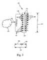
- FIG. 3depicts a cross-sectional view of a simplified block diagram of an apparatus 170 for transmitting and/or receiving optical signals 176 according to one embodiment of the present invention.
- a plurality of optoelectronic converter components or optical components 180 , 182are directly attached or coupled with or formed within the circuit board 174 .
- the optical components 180typically are not encased in a housing and/or packaging. This allows each optical component to be directly integrated with the circuit board 174 .
- the optoelectronic converter componentadditionally includes a substrate (e.g., a ceramic substrate) bonded with the semiconductor optoelectronic converter component before being mounted directly onto the circuit board 174 .
- the circuit boardcan directly generate and receive signals from the optical components. Any number of optical components can be mounted with the circuit board, for example an array of four components formed in a column, two arrays of six components each in rows, and an array of 64 components formed in an 8 ⁇ 8 matrix, are just a few examples of possible configurations.
- the circuit board 174can additionally be coupled with other components, circuits and/or networks 173 , such as a local area network, a PSTN and/or the Internet. Data and/or information 172 can be communicated to and from the circuit board through the network 173 directly, or through one or more intermediate components or circuit boards. Data received from the network can be optically communicated from an optical component 180 over free-space. Optical data detected by an optical component 180 can additionally be forwarded to the network.
- the communication between the circuit board 174 and the networkcan be through substantially any communication technique including electrical, optical, wireless and substantially any other technique.
- Mounting the optical components 180 without packaging and/or housingsignificantly reduces the cost of the optical components as well as reduces the size of the optical components. Further, directly mounting the optical components without packaging allows a larger number of optical components to be attached in the same amount of circuit board real estate. Additionally, eliminating the packaging allows the apparatus 140 to be constructed in a smaller size than previous systems and at a reduced weight. Not only can the apparatus be constructed with a reduced depth 192 due to the direct mounting and the elimination of packaging, but both the lengths and widths (e.g., 194 ) of circuits can be reduced because the optical components require less circuit board real estate. Size and weight can be significant factors in free-space optical communication where transmitters, receiver and/or transceivers are mounted onto buildings or other structures. Reduced size and weight allows for easier mounting on less structure or building real estate with reduced load on the structure or building.
- the optical components 180 , 182can be directly attached or coupled to the circuit board 144 through substantially any method including soldering, bonding, adhesive, socket mounts and substantially any other method for attaching.
- the optical componentsare formed or placed automatically on the circuit board.
- the optical componentsare positioned within predefined tolerances, such as within hundreds of micrometers ( ⁇ m), preferably within tens of ⁇ m, most preferably within less than 10 ⁇ m.
- the positioning of the optical componentscan be achieved through any number of techniques including mechanical positioning, and mechanical positioning utilizing optical alignment. Because the optical components 180 , 182 are precisely aligned on the circuit board 174 , subsequent lateral adjustments of the optical components is typically not necessary.
- One or more optics elements 184are optically aligned and optically coupled with the optical components 180 , 182 .
- each optical component 180 , 182is optically aligned with a separate optics element 184 .
- a plurality of optical componentscan be optically aligned with the same optics element, for example a single large optics element can be aligned with a plurality of laser diodes 182 , as is fully describe below.
- the optics elementsare configured to pass optical signals directly to and from the optical components.
- the optical componentcan be a laser for generating an optical signal that directly impinges an optics element.
- the optics elementconditions the optical signal and passes the optical signal into free-space.
- the optical componentcan be a optical signal detector (e.g., a photo diode) for detecting an optical signal that impinges on an optics element from free-space.
- the optics elementpasses and conditions (e.g., focuses) the free-space optical signal to directly impinge on the optical signal detector.
- the optics 184are mounted or fixed within an optics mount 190 .
- the optics mountsecures the optics together in a single unit. This eliminates the adjustment of each optics element, and reduces the adjustments needed to optimize optical alignment and optical coupling between the optical components 180 , 182 and the optics elements 184 .
- the optics elementsare formed from a single continuous piece (e.g., formed by a molding or stamping process).
- a single plate of plastic, glass or combination of plastic and glasscan incorporate a plurality optics, such as a plurality of lenses, where each optics element aligns with one or more of the optical components 180 , 182 .
- the optical mount 190additionally allows the optics 184 to be mounted with the circuit board 174 .
- the optical mountcan be configured to precisely position the optics 184 at predefined distances 196 from the optical components 180 to maximize the conditioning of the optical signals 176 and the optical communication.
- the distance 196is defined by the laws of optics, such as focal lengths and divergence.
- the optics elements 184are configured with short focal lengths, relative to previous free-space optics elements. As such, the distance 196 at which the optics elements are mounted can be relatively close to the circuit board 174 and optical components 180 , 182 . This results in a further reduction of the depth 197 of the optical communication apparatus 170 .
- the spacing of the plurality of optical components 180 , 182 on the circuit boardis such that divergence of optical signals generated by optical components does not cause interference with neighboring optical components.
- the optical components 180 , 182can be bonded directly onto the circuit board 174 with a separation between components of 30 mm. It will be apparent to one skilled in the art that the spacing of the optical components can be at substantially any distance without departing from the inventive aspects of the present invention.
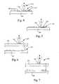
- FIGS. 4 and 5depict simplified block diagrams of a cross-sectional view of a circuit board 202 with an optoelectronic converter component or optical component 204 , such as a laser diode or detector, without a housing mounted and/or fixed directly onto the circuit board.
- the circuit boardincludes additional components 206 , as well as electronics 210 , such as optical component controllers, drivers, receivers and the like.
- the electronics 210couples with the optical component 204 to forward electrical signals to be converted to optical signals 212 through an optical transmitter (e.g., laser diode), or to receive electrical signals converted from optical signals 212 detected by an optical receiver (e.g., detector).
- the coupling between the optical component 204 and the electronics 210can be through substantially any coupling including, but not limited to, a jumper coupling 214 or through a conductor 216 (as shown in FIG. 5 ) routed within the circuit board.
- FIGS. 6 and 7show simplified block diagrams of a cross-sectional view of a circuit board having two layers, or two circuit boards 230 and 231 in cooperation.
- An optoelectronic converter component or optical component 232is attached on the first circuit board 230 .
- An electronic device or electronics 234such as laser driver, signal detector, optical component controller and the like, is attached on the second circuit board 230 .
- the electronics 234couples with the optical component through substantially any means including, but not limited to, a jumper conductor 235 , a conductor 236 routed within the circuit boards (as shown in FIG. 7 ), a through whole via or other such coupling.
- the optical communication apparatuscan be constructed with three layers.
- FIG. 8depicts a simplified block diagram of a cross-section view of an optical communication apparatus 250 according to one embodiment of the present invention.
- a first layer 252includes circuit components and/or electronics, including substantially any electronic device 254 and 256 , such as microchips, capacitors, resistors, power converters, laser drivers and the like.
- the second layer 260includes the optoelectronic converter components 262 for generating or detecting optical signals 264 .
- the first and second layerscan be formed as a single circuit board, as described above. Alternatively, the first and second layers 252 , 260 can be formed through separate circuit boards in cooperation. The second circuit board can be posited below or to the side of the first circuit board opposite optics elements 272 .
- the electronics 256couple with the optoelectronic converter components 262 for delivering electronic signals to the optoelectronic converter components to drive the generation of optical signals 264 , or receiving electrical signals from the optoelectronic converter components generated based on received optical signals 264 .
- a single electronic device 256can couple with a plurality of optoelectronic converter components 262 .
- the third layer 270includes the optics elements 272 .
- the opticsare optically aligned and optically coupled with the optoelectronic converter components 262 .
- the optics 272are formed or mounted within a single structure 270 .
- the optical alignment between the optoelectronic converter components 262 and optics elements 272is greatly simplified because the positioning of the optoelectronic converter components relative to the optics elements is performed once for a plurality of optoelectronic converter components and optics elements. Previous systems required each laser and/or detector to be positioned along the X, Y and Z axes relative to an optics element.
- the plurality of optoelectronic converter components 262can all be adjusted once at the same time relative to the optics elements (or optics elements 272 can all be adjusted at once relative to the optoelectronic converter components).
- the electronic devices 254 , 256 , the optoelectronic converter components 262 and the optics 272can be assembled in a housing, frame or casing 280 .
- the casingprovides structure for the apparatus 250 and maintains positioning of the optics 272 relative to the optoelectronic converter components 262 and/or circuit board 252 .
- the casing 280additional protects the electronics 254 , 256 , optoelectronic converter components 262 and optics 272 from the environment in which the apparatus 250 is utilized.
- the apparatuscan be mounted in or on a building in an urban area and directed to aim at a second transmitter, receiver or transceiver to provide free-space optical communication.
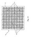
- FIG. 9depicts a simplified block diagram of an overhead view of an optical component array and/or matrix 302 .
- a plurality of optoelectronic converter or optical components 304are distributed across a circuit board 306 .
- a plurality of electronics 310such as optical drivers for driving laser diodes, are included on the circuit board 302 .
- the plurality of electronicscan transmit data signals to the laser diodes to drive or modulate the laser diode in the generation of optical signals.
- the electronics 310are summers coupled with a plurality of optical signal detectors such that the electronics receive data signals from the detectors and sum the signals.
- each of the plurality of electronicscontrols a plurality of optical components.
- the plurality of optoelectronic converter componentscan be distributed on the circuit board such that the optoelectronic convert components alternate every other component between transmitting components and detector components, or some other distribution with both transmitting and detecting components.
- a central electronic device 312activates and/or controls each of the plurality of electronics and/or electronic device 310 , and/or controls a plurality of sub-central electronics 316 which in turn each control a plurality of electronics 310 .
- each of a plurality of optical components 304 controlled by a single electronics 310can be distributed at equal signal distances from the electronics device.
- each of the electronics 310can be distributed at equal distances or signal distances from the sub-central electronic devices 316 or the central electronic device 312
- each of the sub-electronic devicescan be distributed at equal distances from the central electronic device 312 .
- coherence of the signals to and/or from the optical components 304is maintained to synchronize the signals with respect to data transmission and reception, ensuring the signals to and from the central electronic device 312 are received by the central electronic device and reach each of the sub-electronic device 316 (or electronics 310 if directly coupled with the central electronic device) at substantially the same time. Still further, control signals to and from the sub-central electronics are received by the sub-central electronic an reach each of the electronics 310 at substantially the same time, and the signals to and from the electronics 310 are received by the electronics and reach the optical components 304 at substantially the same time. As such, the signal distance between a central electronic device 312 and a plurality of optical components 304 for a given channel are all substantially equal.
- Utilizing a plurality of electronics to each control a plurality of optical componentsallows the apparatus 302 to operate at lower current levels. Operating at lower current levels allows the present apparatus to provide increased data rates. Distributing the optical components 304 at substantially equal signal distances from the electronics 310 maintains coherence between signals to and from the optical components. Further, the signal distances between each of the electronics 310 and the central electronic device 312 are further configured to be substantially equivalent.
- Configuring and cooperating a plurality of optical components onto a circuit boardallows the optical communication apparatus to be configured to generate optical communication paths that span a relatively large diameter. This large diameter allows for the compensation of alignment fluctuations, interference (e.g., caused by objects that can obstruct portions of the communication beam such as birds) and the like. Further, the use of a plurality of optical components allows for the compensation of turbulence, scintillation, interference or drop outs, one or more optical component failures and other effects that can degrade the level of accurate communication.
- the optical componentscan be arranged to provide spatial diversity while still maintaining angular non-diversity. Further, the optical components can be distributed at sufficient distances to achieve uncorrelated communication paths. These advantageous characteristics allow the optical communication apparatus to be very effective in providing free-space optical communication.
- utilizing a plurality of transmit optical componentsallow the communication apparatus to achieve higher total beam power while complying with lower beam power safety regulations.
- a plurality of transmitterscan be set at levels that will not damage the human eye, (e.g., each beam can operate at up to 2 mW/cm 2 (International Electrotechnical Commission (IEC) Class 1M)) while the total beam power of the combined transmitted optical signals is great enough to ensure accurate communication.
- the plurality of low power beamsachieves a total needed power for accurate communication with a low power density.
- FIG. 10depicts a simplified block diagram of a planar view of an optics array or matrix 330 according to one embodiment of the present invention.
- the optics matrixcan be incorporated in an optical communication apparatus (e.g., 140 , 170 , 250 ).
- the optics matrix 330includes a plurality of optics elements 332 that are optically coupled and/or aligned with one or more optoelectronic converter components and/or optical components.
- the optical matrix 330can include a specific number of optics elements 332 such that each optic element 332 aligns with an optical component 304 of an optical component matrix 302 , shown in FIG. 9 .
- the optics elements 332can be discrete optics secured within the matrix, the matrix can be formed as a single continuous piece with the optics elements 332 formed within the continuous piece, or the matrix can be a combination of discrete optics elements and a plurality of optics elements formed in a continuous piece.
- the optics matrix 330can be constructed of substantially any material or combination of materials to provide the desired optical effect.
- the optics matrixcan include a plastic structure 334 with a plurality of optics elements 332 , such as a plurality of plastic lens formed within the plastic structure. Glass can additionally be formed on or bonded with the plastic structure 334 and/or lenses to provide added support and to resist fluctuations or deformations of the lenses and structure due to temperature changes.
- the optics matrix 330whether formed of a single continuous piece, discrete lenses and/or combination thereof, can be formed or assembled in an automated manner. The cooperation of the optics elements 332 within the single optics matrix 330 greatly simplifies the alignment at the same time of the all the optics with the respective plurality of optoelectronic converter components.
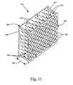
- FIG. 11depicts a simplified block diagram of an elevated view of an optical communication apparatus 350 according to one embodiment of the present invention.
- the apparatusincludes a circuit board 352 with a plurality of optoelectronic converter and/or optical components 354 mounted without packaging directly onto or formed within the circuit board.
- the optoelectronic converter componentsare attached to form a matrix.
- substantially any configurationcan be utilized.
- the optoelectronic converter components 354can be components for generating optical signals 356 and/or for receiving or detecting optical signals 356 .
- the optoelectronic converter components 354can alternate every other component between a transmitting component and a receiving component.
- the apparatus 350includes a substantially planar optics and/or carrier plate 360 , such as an optics matrix (see FIG. 10 ).
- the optics matrix 360includes a plurality of optics elements 362 such as lenses, filters and/or other optics elements.
- a single lens 362is optically coupled and aligned with a single optoelectronic converter component 354 to receive an optical signal 356 from the aligned optoelectronic converter component, and/or to focus an optical signal to impinge on the optoelectronic converter component.
- the optics matrix 360is mounted or secured with the circuit board 352 through supports 364 or a housing.
- the supportsare precisely constructed to provide a separation distance 366 between the circuit board 352 and the optics matrix 360 .
- the distance 366is determined according to the laws of optics, and can be defined by one or more factors including, but not limited to, focal length of the optics elements 362 , proximity of optoelectronic converter components, dimensions of the optoelectronic converter components, divergence of the beam from the optics element, and other factors.
- the focal lengths of the optics elementsare very small relative to optics of other free-space optical communication devices. The small and/or short focal lengths allow for a small separation 366 and thus reduces the overall size of the apparatus 350 .
- the beam divergence transmitted through one or more of the optics elements 362can be adjusted by adjusting the distance 366 between the optics matrix 360 and the optoelectronic converter components 354 .
- the supports 364 and/or housingprovide precise alignment of the optics elements 332 . Further, by utilizing the optics array formed or assembled as a single unit lateral adjustments of the optics elements 332 is avoided.
- FIG. 11shows the circuit board 354 and the optics elements 362 as separate elements.
- the opticsare formed or fixed to the circuit board such that the circuit board includes the optoelectronic converter components as well as the optics.
- a multi-beam moduleis achieved for optical communication, including free-space optical communication.
- the failure of one or more transmitterscan be tolerated when multi-beam transmission is employed. Additionally, the blocking or interference of one or some of the multiple beams can also be tolerated. This results in a high reliability of the communication apparatus.
- the generated optical signalscan be directed and/or conditioned through the optics elements over a free-space link to be received by a receiver.
- the generated optical signalscan be configured such that one or more beams overlap at the receiver. Further, the beams can be defocused to communicate across the link.
- each optical beam generatoris set to transmit at a range of wavelengths. Further, the beam generators can be set up so that different generators transmit at different wavelength ranges. This allows the present invention to reduce or avoid interferometry effects and thus improve communication reliability.
- FIGS. 12–15depict simplified block diagrams of elevated views of some examples of different configurations for the optoelectronic converter components and/or optics according to embodiments of the present invention.
- an optical communication apparatus 380is shown with a matrix or array 382 of optics.
- the matrixis divided into two sub-matrices 384 and 386 .
- Each sub-matrixcan be utilized independent of the other matrix.
- the first matrix 384can be used to transmit a first optical signal
- the second matrix 386is used to receive a second optical signal.
- the first matrix 384can be used to transmit the first optical signal
- the second matrix 386is used to transmit a third optical signal.
- the matricescan be utilized together, for example, both matrices can transmit a first signal.
- the optical signalscan be generated at substantially any power and can be conditioned to achieve a desired signal beam. For example, transmitting at 500 m where each optical signal generated through the array 382 can have a transmit power of +18 dBm with a minimum receive power of ⁇ 37 dBm, the divergence can be limited to 6 mrad with an optical loss of 4 dB, with optical power budget of 51 dB, a geometric loss of 33 dB and a margin of 18 dB. Other configurations and power levels can be utilized to achieve a desired implementation.
- FIG. 13shows an optical communication apparatus 402 with a matrix 404 of optics elements 405 and/or optoelectronic converter components.
- the matrixincludes four sub-matrices 406 , 410 , 412 , 414 .
- Each sub-matrixcan be utilized independent of the other matrices.
- the first matrix 406can be used to transmit a first optical signal
- the second matrix 410can be used to transmit a second optical signal
- the third matrix 412can be used to transmit a third optical signal
- the fourth matrix 414can be used to transmit a fourth optical signal.
- the first matrix 406can be used to transmit the first optical signal
- the second matrix 410can be used to transmit the second optical signal
- the third matrix 412can be used receive a third optical signal
- the fourth matrix 414can be used to receive a fourth optical signal.
- the apparatus shown in FIG. 13can be configured to communicate at 155 Mbps, transmitting over a distance of 300 m where each optical signal generated through the array 402 can have a transmit power of +15 dBm with a minimum receive power of ⁇ 37 dBm, the divergence can be limited to 6 mrad with an optical loss of 6 dB, with an optical power budget of 46 dB, a geometric loss of 31 dB and a margin of 15 dB.
- FIG. 14shows an optical communication apparatus 420 with a matrix 422 of optics elements as well as a first large optic element 424 and a second large optic element 426 .
- each optic element of the matrix 422can be optically coupled and aligned with a single optical component
- each of the first and second optics elementsare optically coupled and aligned with a plurality of optoelectronic converter components and/or optical components.
- the first and/or second large optics elementscan optically couple and align with a single optical component.
- the optics elementscan be associated with separate and different signal channels that carry logically separate information encoded, for example, on different wavelengths or with different polarizations.
- the matrix 422can be divided into any number of sub-matrices as described above.
- the communication through the matrix and the two large opticscan be configured in substantially any configuration.
- the first large optic 424can transmit a first optical signal
- the second large optic 426can transmit a second optical signal
- the matrix 422can receive a third optical signal.
- the first large opticcan receive a first optical signal
- the second large opticcan transmit a second optical signal
- the matrix 422can transmit a third optical signal.
- FIG. 15shows an optical communication apparatus 440 with a matrix 442 of optics elements as well as a large optic element 444 .
- the matrix 422can be divided into any number of sub-matrices.
- the communication through the matrix and the large opticcan be configured in substantially any configuration.
- the large optic 444can transmit a first optical signal and the matrix 442 can receive a second optical signal.
- the large optic 444can receive a first optical signal and the matrix 442 can transmit a second optical signal.
- Other combinationscan be used without departing from the inventive aspects of the present invention.
- FIG. 16depicts a simplified block diagram of an elevated view of an optical communication apparatus 450 according to one embodiment of the present invention.
- the apparatus 450includes a plurality of sub-apparatuses 452 , 460 , 466 and 474 that are stacked and/or combined.
- the sub-apparatusesare similar to the apparatus 440 shown in FIG. 15 .
- any sub-apparatus or combination of sub-apparatusescan be utilized in the assembly of the communication apparatus 450 .
- each sub-apparatusincludes a matrix of optics elements 454 , 462 , 470 and 476 , as well as a large optic element 456 , 464 , 472 and 480 .
- the matrix of optics and the large optic in each sub-apparatuscan be used to transmit and/or receive optical signals. Further, each matrix can be divided into sub-matrices as described above.
- a first signalcan be transmitted by the matrices 454 , 462 , 470 , and 476 while a second signal can be received by the large optic elements 456 , 464 , 472 and 480 .
- the optical signalscan be generated at substantially any power and can be conditioned to achieve a desired signal beam.
- the apparatus 450can transmit at 2000 m where each optical signal generated can have a transmit power of +27 dBm with a minimum receive power of ⁇ 37 dBm, the divergence can be limited to 6 mrad with an optical loss of 4 dB, with optical power budget of 60 dB, a geometric loss of 34 dB and a margin of 26 dB.
- each sub-apparatuses 452 , 460 , 466 and 474can generate communication signals providing, for example, 155 Mbps data rates and greater.
- FIG. 17depicts a simplified block diagram of a cross-sectional view of an optical communication apparatus 502 according to one embodiment of the present invention.
- the apparatus 502includes a plurality of small optics elements 504 that are optically coupled and aligned with at least one optoelectronic converter component and/or optical component 506 , such as a laser, detector or the like.
- Each optoelectronic converter component 506is directly mounted on a first circuit board 510 to receive and/or transmit communication data through optical signals 508 .
- the small optics elements 504are configured to have short focal lengths 512 , relative to optics incorporated in previous optical communication devices, and particularly previous free-space optical communication devices.
- the apparatus 502additionally includes a large optics element 514 .
- the large optic elementis optically coupled with one or more optoelectronic converter components 516 .
- the one or more optoelectronic converter components 516are directly mounted onto a second circuit board 520 .
- the second circuit board 520can be an independent circuit board from the first circuit board 510 , or the second circuit board 520 can be a part of a single circuit board containing both the first and second circuit boards 510 , 520 , respectively.
- the large optic element 514has a focal length 522 that is longer and/or larger than the short focal length 512 of the small optics 504 .
- the longer focal length 522is typically similar to the focal lengths of optics elements incorporated in previous free-space optical communication devices.
- the second circuit board 520is offset from the first circuit board 510 , or the first and second circuit boards are assembled on a single plane and the large optic 514 is positioned out further from the circuit boards 510 and 520 than the small optics 504 .
- the large optic elementhaving the longer focal length 522 , the depth 524 of the apparatus 502 is larger than if just small optics elements 504 had been utilized.
- the present inventioncan be implemented to provide free-space optical communication.
- Two transceivers assembled, such as those described above or other configurations where optoelectronic converter components are mounted directly onto a circuit board,can be aligned with each other on opposite sides of a free-space link.
- optical communicationcan be provided between the transceivers.
- the transceiverscan employ a plurality of small optics elements, one or more large optics and/or a combination of small and large optics elements.
- FIG. 18depicts a simplified block diagram of a free-space optical communication network 560 for providing communication according to one embodiment of the present invention.
- a plurality of optical transceivers 562are distributed around an area, for example distributed through a metropolitan area.
- the transceiverscan be mounted on or within buildings 564 , towers 566 and other structures.
- the transceiversare configured according to one embodiment to include a plurality of optoelectronic converter devices aligned with a plurality of optics elements to generate a plurality of free-space optical signals 568 . Because the present invention provides free-space optical communication apparatuses that can have decreased weights and size relative to previous free-space optical communication devices the present apparatuses can be mounted in positions that were previously unavailable.
- communication apparatusescan be mounted on the sides of building, on structures than cannot support excess weights and in other locations previously unavailable. Further, because the present apparatuses can have a reduced size and weight, the apparatuses can be mounted within buildings without adversely affecting views and without affecting the aesthetics of the building interior.
- the transceivers 562are optically aligned to transmit and/or receive the optical signals 568 to provide communication of data and/or information across the network.
- the transceivers 562can be coupled with routers 570 or other signal distribution devices within or on the builds, or coupled with (or part of) a communication network 572 .
- the routers 570are show on the buildings; however, typically, the routers are located within the building or other structures.
- the routers 570can supply optical or electrical data signals to the transceiver to be communicated optically over the free-space, or to receive optical or electrical signals converted by the transceiver from the received free-space optical signals.
- the routers 570can route signals within the build and/or be coupled with the communication network 572 , such as a fiber optic network, a PSTN or other network.
- the present inventionprovides free-space optical signal transmitters, receivers and/or transceivers with reduced dimensions over previous transmitters, receivers and transceivers.
- Directly incorporating the plurality of optical components onto the circuit boardallows for the elimination of the packaging and fiber optic coupling or connections of previous devices.
- smaller optics elementsare employed that are secured relative to the circuit board.
- the optics elementsare designed to have small focal lengths, reducing the distance at which the optics are fixed relative to the circuit board and optical components. This again results in the ability to further reduce the size of the transmitters, receivers and/or transceivers of the present invention.
- the incorporation of optical components without package and fiber optic connectionsreduces the weight of the transmitter, receiver and/or transceiver of the present invention. Further, the use of the small optics further reduces the weight of the present invention. Still further, the reduced dimensions of the apparatus results in less material needed for the structure and to house the transmitter, receiver, and/or transceiver of the present invention, resulting in further reduced weight. Thus, the present invention provides a lighter apparatus for optical communication.
- the reduced size and weightallow the present apparatus to be mounted easier, at reduced costs, and in locations that previously were not accessible by previous systems. Still further, the reduced size translates to reduced area of a building or structure needed to mount the present apparatus as well as providing aesthetic benefits to the end-user.
- the present inventionUtilizing optical components that do not have packaging or fiber optic coupling, allows the present invention to be constructed at reduced costs over previous devices. Further, the present invention utilizes a plurality of low power optical components to achieve the desired receive power while maintaining low power density levels. The cost of low power transmitters is significantly less than higher power transmitters further reducing the cost of the present invention over previous systems delivering the same optical power at the receiver.
- the mounting of the optical components onto the circuit boardcan be achieved through mechanical means.
- the present inventioncan be produced in volume at significantly reduced costs.
- the present inventioncan be constructed at costs less than previous systems.
- the present inventionemploys a plurality of low power optical signals, distributed over an area resulting in low power density that meets eye safety regulations. Further, the use of the plurality of low power optical signals sum to provide the needed optical power at the receiver. Still further, utilizing a plurality of optical components (e.g., generating a plurality of free-space optical signals) allows the apparatus to tolerate one or more transmitter and/or receiver optical component failures, turbulence, and interference.
- the present inventioncan be constructed to have dimensions which further provide for incoherency to improve communication.
- the present inventionis capable of utilizing reduced currents to drive the transmitters. Reduced currents allow for higher data rates because fewer electrons are being forced through the conducts. Thus the present invention achieves increased communication data rates.
- the apparatusutilizes optical components mounted or formed directly on the circuit board eliminating the three-coordinate (X, Y and Z) adjustments of each optical component. Further, in some embodiments, the present invention employs the array of optics elements secured together which additionally eliminates the need to three-dimensionally align each optic.
Landscapes
- Physics & Mathematics (AREA)
- Electromagnetism (AREA)
- Engineering & Computer Science (AREA)
- Computer Networks & Wireless Communication (AREA)
- Signal Processing (AREA)
- Optical Communication System (AREA)
- Optical Couplings Of Light Guides (AREA)
Abstract
Description
Claims (19)
Priority Applications (4)
| Application Number | Priority Date | Filing Date | Title |
|---|---|---|---|
| US10/218,684US7106973B2 (en) | 2002-08-13 | 2002-08-13 | Apparatus and method for use in free-space optical communication comprising optically aligned components integrated on circuit boards |
| EP03784742AEP1532755A4 (en) | 2002-08-13 | 2003-06-17 | Appartus and method for free-space optical communication |
| PCT/US2003/018969WO2004015451A2 (en) | 2002-08-13 | 2003-06-17 | Appartus and method for free-space optical communication |
| AU2003253650AAU2003253650A1 (en) | 2002-08-13 | 2003-06-17 | Appartus and method for free-space optical communication |
Applications Claiming Priority (1)
| Application Number | Priority Date | Filing Date | Title |
|---|---|---|---|
| US10/218,684US7106973B2 (en) | 2002-08-13 | 2002-08-13 | Apparatus and method for use in free-space optical communication comprising optically aligned components integrated on circuit boards |
Publications (2)
| Publication Number | Publication Date |
|---|---|
| US20040033078A1 US20040033078A1 (en) | 2004-02-19 |
| US7106973B2true US7106973B2 (en) | 2006-09-12 |
Family
ID=31714582
Family Applications (1)
| Application Number | Title | Priority Date | Filing Date |
|---|---|---|---|
| US10/218,684Expired - LifetimeUS7106973B2 (en) | 2002-08-13 | 2002-08-13 | Apparatus and method for use in free-space optical communication comprising optically aligned components integrated on circuit boards |
Country Status (4)
| Country | Link |
|---|---|
| US (1) | US7106973B2 (en) |
| EP (1) | EP1532755A4 (en) |
| AU (1) | AU2003253650A1 (en) |
| WO (1) | WO2004015451A2 (en) |
Cited By (23)
| Publication number | Priority date | Publication date | Assignee | Title |
|---|---|---|---|---|
| US20060200598A1 (en)* | 2004-04-08 | 2006-09-07 | Janzen Jeffery W | System and method for optimizing interconnections of components in a multichip memory module |
| US20070031149A1 (en)* | 2005-08-05 | 2007-02-08 | Hiroyuki Sasai | Space optical transmission apparatus and space optical transimission system |
| US7254331B2 (en) | 2002-08-09 | 2007-08-07 | Micron Technology, Inc. | System and method for multiple bit optical data transmission in memory systems |
| US7266633B2 (en) | 2004-05-17 | 2007-09-04 | Micron Technology, Inc. | System and method for communicating the synchronization status of memory modules during initialization of the memory modules |
| US7282947B2 (en) | 2003-06-11 | 2007-10-16 | Micron Technology, Inc. | Memory module and method having improved signal routing topology |
| US7289347B2 (en) | 2002-08-02 | 2007-10-30 | Micron Technology, Inc. | System and method for optically interconnecting memory devices |
| US7366864B2 (en) | 2004-03-08 | 2008-04-29 | Micron Technology, Inc. | Memory hub architecture having programmable lane widths |
| US7370134B2 (en) | 2004-03-25 | 2008-05-06 | Micron Technology, Inc. | System and method for memory hub-based expansion bus |
| US7392331B2 (en) | 2004-08-31 | 2008-06-24 | Micron Technology, Inc. | System and method for transmitting data packets in a computer system having a memory hub architecture |
| US7461286B2 (en) | 2003-10-27 | 2008-12-02 | Micron Technology, Inc. | System and method for using a learning sequence to establish communications on a high-speed nonsynchronous interface in the absence of clock forwarding |
| US20090110406A1 (en)* | 2007-10-24 | 2009-04-30 | Terrel Morris | Dynamic optical signal tracking on a detector array in a free space optical communication system |
| US7546435B2 (en) | 2004-02-05 | 2009-06-09 | Micron Technology. Inc. | Dynamic command and/or address mirroring system and method for memory modules |
| US7805586B2 (en) | 2002-08-29 | 2010-09-28 | Micron Technology, Inc. | System and method for optimizing interconnections of memory devices in a multichip module |
| US7831151B2 (en)* | 2001-06-29 | 2010-11-09 | John Trezza | Redundant optical device array |
| US20130182620A1 (en)* | 2012-01-09 | 2013-07-18 | Attochron Llc | Uspl-fso lasercom point-to-point and point-to-multipoint optical wireless communication |
| US8589643B2 (en) | 2003-10-20 | 2013-11-19 | Round Rock Research, Llc | Arbitration system and method for memory responses in a hub-based memory system |
| US9654222B1 (en) | 2015-12-30 | 2017-05-16 | Surefire Llc | Transmitters for optical narrowcasting |
| US9853740B1 (en) | 2017-06-06 | 2017-12-26 | Surefire Llc | Adaptive communications focal plane array |
| US10225011B1 (en) | 2017-04-05 | 2019-03-05 | X Development Llc | Free-space optical communications network |
| US10236986B1 (en) | 2018-01-05 | 2019-03-19 | Aron Surefire, Llc | Systems and methods for tiling free space optical transmissions |
| US10250948B1 (en) | 2018-01-05 | 2019-04-02 | Aron Surefire, Llc | Social media with optical narrowcasting |
| US10473439B2 (en) | 2018-01-05 | 2019-11-12 | Aron Surefire, Llc | Gaming systems and methods using optical narrowcasting |
| WO2021058834A1 (en)* | 2019-09-27 | 2021-04-01 | Purelifi Limited | Optical wireless communication (owc) unit |
Families Citing this family (13)
| Publication number | Priority date | Publication date | Assignee | Title |
|---|---|---|---|---|
| US20040120717A1 (en)* | 2002-12-18 | 2004-06-24 | Lightpointe Communications, Inc. | Extended source free-space optical communication system |
| JP2004260817A (en)* | 2003-02-27 | 2004-09-16 | Amtran Technology Co Ltd | Radio signal transceiver system |
| US20050129407A1 (en)* | 2003-12-10 | 2005-06-16 | Coleman Christopher L. | Imaging lens for multi-channel free-space optical interconnects |
| DE102006014848A1 (en)* | 2006-03-30 | 2007-10-04 | Rohde & Schwarz Gmbh & Co. Kg | Optical data bus for e.g. wireless device, is provided between modules, where diode emits light beams perpendicularly to longitudinal direction of modules and direction is changed by tilted/turned arrangement of diode within transmitter |
| CN100454787C (en)* | 2006-04-14 | 2009-01-21 | 南京邮电大学 | Device and method for positioning and aligning an antenna of a free-space optical communication system |
| DE102007017016B4 (en)* | 2007-04-11 | 2012-02-02 | Fraunhofer-Gesellschaft zur Förderung der angewandten Forschung e.V. | Optoelectronic device and method for its construction |
| ES2487621T3 (en) | 2009-05-06 | 2014-08-22 | Tesat Spacecom Gmbh & Co. Kg | Hybrid communication device for high-speed data transmission between mobile platforms and / or stationary platforms |
| JP5743420B2 (en)* | 2010-04-20 | 2015-07-01 | 株式会社東芝 | X-ray CT system |
| US10373998B1 (en) | 2013-03-14 | 2019-08-06 | Wavefront Research, Inc. | Compact annular field imager optical interconnect |
| DE102015221283B4 (en)* | 2015-10-30 | 2017-09-14 | Deutsches Zentrum für Luft- und Raumfahrt e.V. | Transmitter for a free beam optical communication system and associated receiver terminal |
| US11381314B2 (en) | 2018-01-26 | 2022-07-05 | Bridgecomm, Inc. | Free space optical communication systems and methods for QOS control |
| WO2021178746A1 (en)* | 2020-03-05 | 2021-09-10 | Bridgecomm, Inc. | Free space optical communication systems and methods for qos control |
| CN114624874B (en)* | 2020-12-08 | 2023-11-10 | 军事科学院系统工程研究院网络信息研究所 | Optical fiber-space optical communication signal conversion method based on chip integrated optical circuit |
Citations (52)
| Publication number | Priority date | Publication date | Assignee | Title |
|---|---|---|---|---|
| US4428647A (en) | 1982-11-04 | 1984-01-31 | Xerox Corporation | Multi-beam optical system using lens array |
| US4469443A (en) | 1982-06-01 | 1984-09-04 | The United States Of America As Represented By The Secretary Of The Navy | Atmospheric transmissometer |
| US4639586A (en) | 1985-02-06 | 1987-01-27 | The United States Of America As Represented By The Secretary Of The Air Force | Optically phased laser transmitter |
| US4689482A (en) | 1984-06-13 | 1987-08-25 | Fuji Photo Film Co., Ltd. | Multiple laser beam scanner with beam intensity control |
| US4709413A (en) | 1982-09-10 | 1987-11-24 | American Telephone And Telegraph Company, At&T Bell Laboratories | Bidirectional fiber optic systems |
| US4761059A (en) | 1986-07-28 | 1988-08-02 | Rockwell International Corporation | External beam combining of multiple lasers |
| US4794345A (en) | 1986-02-26 | 1988-12-27 | Trw Inc. | Phased array combination of laser beams |
| US4823357A (en) | 1986-11-10 | 1989-04-18 | The United States Of America As Represented By The Secretary Of The Air Force | Diffraction limited dichroic combiner diode laser |
| US4826269A (en) | 1987-10-16 | 1989-05-02 | Spectra Diode Laboratories, Inc. | Diode laser arrangement forming bright image |
| US4922502A (en) | 1987-06-30 | 1990-05-01 | Hoya Corporation | Solid-state laser device comprising a plurality of excitation units selectively energized |
| US5142400A (en) | 1989-12-26 | 1992-08-25 | Cubic Corporation | Method and apparatus for automatic acquisition and alignment of an optical beam communication link |
| US5227906A (en)* | 1989-03-09 | 1993-07-13 | Canon Kabushiki Kaisha | Optical switch array capable of bidirectional signal transfer between a plurality of terminals |
| US5264955A (en) | 1989-01-09 | 1993-11-23 | Canon Kabushiki Kaisha | Optical space communication apparatus |
| US5267010A (en) | 1989-10-17 | 1993-11-30 | Kremer Richard M | Laser radar device |
| US5268978A (en) | 1992-12-18 | 1993-12-07 | Polaroid Corporation | Optical fiber laser and geometric coupler |
| US5280184A (en)* | 1992-04-08 | 1994-01-18 | Georgia Tech Research Corporation | Three dimensional integrated circuits with lift-off |
| US5311535A (en) | 1992-07-28 | 1994-05-10 | Karpinski Arthur A | Monolithic laser diode array providing emission from a minor surface thereof |
| US5327274A (en)* | 1991-08-13 | 1994-07-05 | Sharp Kabushiki Kaisha | Optical calculating apparatus |
| US5394489A (en) | 1993-07-27 | 1995-02-28 | At&T Corp. | Wavelength division multiplexed optical communication transmitters |
| US5416861A (en)* | 1994-04-29 | 1995-05-16 | University Of Cincinnati | Optical synchronous clock distribution network and high-speed signal distribution network |
| US5465170A (en) | 1993-01-19 | 1995-11-07 | Atr Optical And Radio Communications Research Lab. | Alignment adjusting system for use in optical system of optical transceiver |
| US5501385A (en) | 1994-12-08 | 1996-03-26 | The United States Of America As Represented By The United States Department Of Energy | Large core fiber optic cleaver |
| US5513021A (en)* | 1993-11-09 | 1996-04-30 | Hewlett-Packard Company | Optical detectors and sources with merged holographic optical elements suitable for optoelectronic interconnects |
| US5521736A (en) | 1994-09-29 | 1996-05-28 | Vixel Corporation | Control circuits for parallel optical interconnects |
| US5548772A (en)* | 1991-12-18 | 1996-08-20 | Texas Instruments Incorporated | Parallel processing system with programmable optical interconnects |
| US5661584A (en)* | 1994-11-16 | 1997-08-26 | Nec Research Institute, Inc. | Optoelectronic apparatus |
| US5710652A (en) | 1992-08-27 | 1998-01-20 | Trex Communications | Laser communication transceiver and system |
| US5715339A (en) | 1992-04-23 | 1998-02-03 | Hitachi, Ltd. | Optical parallel transmission device |
| US5764677A (en) | 1994-09-01 | 1998-06-09 | The United States Of America As Represented By The Secretary Of The Navy | Laser diode power combiner |
| US5777768A (en) | 1995-09-01 | 1998-07-07 | Astroterra Corporation | Multiple transmitter laser link |
| US5818984A (en)* | 1996-11-18 | 1998-10-06 | International Business Machines Corporation | Optoelectronic interconnection of integrated circuits |
| US5857042A (en)* | 1997-04-29 | 1999-01-05 | Mcgill University | Optical interconnection arrangements |
| US5943456A (en) | 1997-08-20 | 1999-08-24 | Lucent Technologies Inc. | Coarse wavelength division multiplexing optical system |
| US6005700A (en) | 1996-06-26 | 1999-12-21 | Aironet Wireless Communications, Inc. | Computer peripheral device with detachable portion and light display |
| WO2001005069A2 (en)* | 1999-07-08 | 2001-01-18 | Quantumbeam Limited | Optical free space signalling system |
| US6203211B1 (en) | 1999-04-27 | 2001-03-20 | Yu-Feng Cheng | Connector for a fiber optic cable |
| US6239888B1 (en) | 1998-04-24 | 2001-05-29 | Lightpointe Communications, Inc. | Terrestrial optical communication network of integrated fiber and free-space links which requires no electro-optical conversion between links |
| US6272271B1 (en)* | 1999-04-29 | 2001-08-07 | General Electric Company | Alignment of optical interfaces for data communication |
| US6323980B1 (en)* | 1998-03-05 | 2001-11-27 | Air Fiber, Inc. | Hybrid picocell communication system |
| US6327291B1 (en) | 1995-11-22 | 2001-12-04 | Iridex Corporation | Fiber stub end-pumped laser |
| US6398425B2 (en)* | 2000-05-09 | 2002-06-04 | Teraconnect, Inc | Self aligning optical interconnect with multiple opto-electronic devices per fiber channel |
| US20020094187A1 (en) | 2001-01-16 | 2002-07-18 | Todd Barrett | Variable optical attenuator |
| US6429981B2 (en)* | 2000-02-22 | 2002-08-06 | Pioneer Corporation | Optical pickup apparatus |
| US20020126340A1 (en) | 2001-03-01 | 2002-09-12 | Nikiforov Evgeny Alexeevich | Wireless duplex optical communication system |
| US6452700B1 (en)* | 2001-01-11 | 2002-09-17 | R&Dm Foundation | Computer backplane employing free space optical interconnect |
| US6493121B1 (en)* | 1998-04-30 | 2002-12-10 | Infineon Technologies Ag | Bidirectional module for multichannel use |
| US6509992B1 (en)* | 1999-09-09 | 2003-01-21 | Nortel Networks Corporation | Free space optical interconnect system tolerant to misalignments and method of operation thereof |
| US6583904B1 (en)* | 1999-10-01 | 2003-06-24 | Eci Telecom Ltd. | Method and apparatus for aligning optical interconnections between printed circuit boards |
| US6587618B2 (en) | 2001-03-16 | 2003-07-01 | Corning Incorporated | Collimator array and method and system for aligning optical fibers to a lens array |
| US6657783B1 (en) | 2000-10-05 | 2003-12-02 | Lucent Technologies Inc. | Method and apparatus for aligning telescopes within a free-space optical communication system |
| US20040120717A1 (en) | 2002-12-18 | 2004-06-24 | Lightpointe Communications, Inc. | Extended source free-space optical communication system |
| US6968133B2 (en) | 2000-05-15 | 2005-11-22 | Canon Kabushiki Kaisha | Optical free-space communication apparatus |
- 2002
- 2002-08-13USUS10/218,684patent/US7106973B2/ennot_activeExpired - Lifetime
- 2003
- 2003-06-17EPEP03784742Apatent/EP1532755A4/ennot_activeWithdrawn
- 2003-06-17AUAU2003253650Apatent/AU2003253650A1/ennot_activeAbandoned
- 2003-06-17WOPCT/US2003/018969patent/WO2004015451A2/ennot_activeApplication Discontinuation
Patent Citations (53)
| Publication number | Priority date | Publication date | Assignee | Title |
|---|---|---|---|---|
| US4469443A (en) | 1982-06-01 | 1984-09-04 | The United States Of America As Represented By The Secretary Of The Navy | Atmospheric transmissometer |
| US4709413A (en) | 1982-09-10 | 1987-11-24 | American Telephone And Telegraph Company, At&T Bell Laboratories | Bidirectional fiber optic systems |
| US4428647A (en) | 1982-11-04 | 1984-01-31 | Xerox Corporation | Multi-beam optical system using lens array |
| US4689482A (en) | 1984-06-13 | 1987-08-25 | Fuji Photo Film Co., Ltd. | Multiple laser beam scanner with beam intensity control |
| US4639586A (en) | 1985-02-06 | 1987-01-27 | The United States Of America As Represented By The Secretary Of The Air Force | Optically phased laser transmitter |
| US4794345A (en) | 1986-02-26 | 1988-12-27 | Trw Inc. | Phased array combination of laser beams |
| US4761059A (en) | 1986-07-28 | 1988-08-02 | Rockwell International Corporation | External beam combining of multiple lasers |
| US4823357A (en) | 1986-11-10 | 1989-04-18 | The United States Of America As Represented By The Secretary Of The Air Force | Diffraction limited dichroic combiner diode laser |
| US4922502A (en) | 1987-06-30 | 1990-05-01 | Hoya Corporation | Solid-state laser device comprising a plurality of excitation units selectively energized |
| US4826269A (en) | 1987-10-16 | 1989-05-02 | Spectra Diode Laboratories, Inc. | Diode laser arrangement forming bright image |
| US5264955A (en) | 1989-01-09 | 1993-11-23 | Canon Kabushiki Kaisha | Optical space communication apparatus |
| US5227906A (en)* | 1989-03-09 | 1993-07-13 | Canon Kabushiki Kaisha | Optical switch array capable of bidirectional signal transfer between a plurality of terminals |
| US5267010A (en) | 1989-10-17 | 1993-11-30 | Kremer Richard M | Laser radar device |
| US5142400A (en) | 1989-12-26 | 1992-08-25 | Cubic Corporation | Method and apparatus for automatic acquisition and alignment of an optical beam communication link |
| US5327274A (en)* | 1991-08-13 | 1994-07-05 | Sharp Kabushiki Kaisha | Optical calculating apparatus |
| US5548772A (en)* | 1991-12-18 | 1996-08-20 | Texas Instruments Incorporated | Parallel processing system with programmable optical interconnects |
| US5280184A (en)* | 1992-04-08 | 1994-01-18 | Georgia Tech Research Corporation | Three dimensional integrated circuits with lift-off |
| US5715339A (en) | 1992-04-23 | 1998-02-03 | Hitachi, Ltd. | Optical parallel transmission device |
| US5311535A (en) | 1992-07-28 | 1994-05-10 | Karpinski Arthur A | Monolithic laser diode array providing emission from a minor surface thereof |
| US5710652A (en) | 1992-08-27 | 1998-01-20 | Trex Communications | Laser communication transceiver and system |
| US5268978A (en) | 1992-12-18 | 1993-12-07 | Polaroid Corporation | Optical fiber laser and geometric coupler |
| US5465170A (en) | 1993-01-19 | 1995-11-07 | Atr Optical And Radio Communications Research Lab. | Alignment adjusting system for use in optical system of optical transceiver |
| US5394489A (en) | 1993-07-27 | 1995-02-28 | At&T Corp. | Wavelength division multiplexed optical communication transmitters |
| US5513021A (en)* | 1993-11-09 | 1996-04-30 | Hewlett-Packard Company | Optical detectors and sources with merged holographic optical elements suitable for optoelectronic interconnects |
| US5416861A (en)* | 1994-04-29 | 1995-05-16 | University Of Cincinnati | Optical synchronous clock distribution network and high-speed signal distribution network |
| US5764677A (en) | 1994-09-01 | 1998-06-09 | The United States Of America As Represented By The Secretary Of The Navy | Laser diode power combiner |
| US5521736A (en) | 1994-09-29 | 1996-05-28 | Vixel Corporation | Control circuits for parallel optical interconnects |
| US5661584A (en)* | 1994-11-16 | 1997-08-26 | Nec Research Institute, Inc. | Optoelectronic apparatus |
| US5501385A (en) | 1994-12-08 | 1996-03-26 | The United States Of America As Represented By The United States Department Of Energy | Large core fiber optic cleaver |
| US5777768A (en) | 1995-09-01 | 1998-07-07 | Astroterra Corporation | Multiple transmitter laser link |
| US6327291B1 (en) | 1995-11-22 | 2001-12-04 | Iridex Corporation | Fiber stub end-pumped laser |
| US6005700A (en) | 1996-06-26 | 1999-12-21 | Aironet Wireless Communications, Inc. | Computer peripheral device with detachable portion and light display |
| US5818984A (en)* | 1996-11-18 | 1998-10-06 | International Business Machines Corporation | Optoelectronic interconnection of integrated circuits |
| US5857042A (en)* | 1997-04-29 | 1999-01-05 | Mcgill University | Optical interconnection arrangements |
| US5943456A (en) | 1997-08-20 | 1999-08-24 | Lucent Technologies Inc. | Coarse wavelength division multiplexing optical system |
| US6323980B1 (en)* | 1998-03-05 | 2001-11-27 | Air Fiber, Inc. | Hybrid picocell communication system |
| US6239888B1 (en) | 1998-04-24 | 2001-05-29 | Lightpointe Communications, Inc. | Terrestrial optical communication network of integrated fiber and free-space links which requires no electro-optical conversion between links |
| US6462847B2 (en) | 1998-04-24 | 2002-10-08 | Lightpointe Communications, Inc. | Method and apparatus for free-space optical communication without electro-optical conversion |
| US6493121B1 (en)* | 1998-04-30 | 2002-12-10 | Infineon Technologies Ag | Bidirectional module for multichannel use |
| US6203211B1 (en) | 1999-04-27 | 2001-03-20 | Yu-Feng Cheng | Connector for a fiber optic cable |
| US6272271B1 (en)* | 1999-04-29 | 2001-08-07 | General Electric Company | Alignment of optical interfaces for data communication |
| WO2001005069A2 (en)* | 1999-07-08 | 2001-01-18 | Quantumbeam Limited | Optical free space signalling system |
| US6509992B1 (en)* | 1999-09-09 | 2003-01-21 | Nortel Networks Corporation | Free space optical interconnect system tolerant to misalignments and method of operation thereof |
| US6583904B1 (en)* | 1999-10-01 | 2003-06-24 | Eci Telecom Ltd. | Method and apparatus for aligning optical interconnections between printed circuit boards |
| US6429981B2 (en)* | 2000-02-22 | 2002-08-06 | Pioneer Corporation | Optical pickup apparatus |
| US6398425B2 (en)* | 2000-05-09 | 2002-06-04 | Teraconnect, Inc | Self aligning optical interconnect with multiple opto-electronic devices per fiber channel |
| US6968133B2 (en) | 2000-05-15 | 2005-11-22 | Canon Kabushiki Kaisha | Optical free-space communication apparatus |
| US6657783B1 (en) | 2000-10-05 | 2003-12-02 | Lucent Technologies Inc. | Method and apparatus for aligning telescopes within a free-space optical communication system |
| US6452700B1 (en)* | 2001-01-11 | 2002-09-17 | R&Dm Foundation | Computer backplane employing free space optical interconnect |
| US20020094187A1 (en) | 2001-01-16 | 2002-07-18 | Todd Barrett | Variable optical attenuator |
| US20020126340A1 (en) | 2001-03-01 | 2002-09-12 | Nikiforov Evgeny Alexeevich | Wireless duplex optical communication system |
| US6587618B2 (en) | 2001-03-16 | 2003-07-01 | Corning Incorporated | Collimator array and method and system for aligning optical fibers to a lens array |
| US20040120717A1 (en) | 2002-12-18 | 2004-06-24 | Lightpointe Communications, Inc. | Extended source free-space optical communication system |
Non-Patent Citations (8)
| Title |
|---|
| E. Korevaar et al., "Status of SDIO-IS&T Lasercom Testbed Program", Society of Photo-Optical Instrumentation Engineers, vol. 1866, pp. 116-127 (Jan. 20-21, 1993). |
| E. Korevaar et al.; "Design of Satellite Terminal for BMDO Lasercom Technology Demonstration"; Society of Photo-Optical Instrumentation Engineers, vol. 2381; pp. 60-71 (Feb. 7-8, 1995). |
| J. Schuster et al.; "Optomechanical Design of STRV-2 Lasercom Transceiver Using Novel Azimuth-Slant Gimbal"; Society of Photo-Optical Instrumentation Engineers, vol. 2699; pp. 227-239 (Jan. 30-31, 1996). |
| Kim et al.; "Scintillation Reduction Using Multiple Transmitters"; Society of Photo-Optical Instrumentation Engineers, vol. 2990; pp. 102-113 (1997). |
| Patent Cooperation Treaty, "PCT International Preliminary Examination Report", dated Oct. 13, 2004, for corresponding PCT Application No. PCT/US03/18969, 14 pages. |
| Patent Cooperation Treaty, "PCT International Search Report", dated Dec. 15, 2003, for corresponding PCT Application No. PCT/US03/18969, 3 pages. |
| Patent Cooperation Treaty, "PCT Written Opinion", dated May 7, 2004, for corresponding PCT Application No. PCT/US03/18969, 7 pages. |
| W. M. Bruno et al.; "Diode Laser Spatial Diversity Transmitter"; Society of Photo-Optical Instrumentation Engineers, vol. 1044; pp. 187-194 (1989). |
Cited By (67)
| Publication number | Priority date | Publication date | Assignee | Title |
|---|---|---|---|---|
| US7831151B2 (en)* | 2001-06-29 | 2010-11-09 | John Trezza | Redundant optical device array |
| US7289347B2 (en) | 2002-08-02 | 2007-10-30 | Micron Technology, Inc. | System and method for optically interconnecting memory devices |
| US7411807B2 (en)* | 2002-08-02 | 2008-08-12 | Micron Technology, Inc. | System and method for optically interconnecting memory devices |
| US7382639B2 (en) | 2002-08-02 | 2008-06-03 | Micron Technology, Inc. | System and method for optically interconnecting memory devices |
| US7489875B2 (en) | 2002-08-09 | 2009-02-10 | Micron Technology, Inc. | System and method for multiple bit optical data transmission in memory systems |
| US7254331B2 (en) | 2002-08-09 | 2007-08-07 | Micron Technology, Inc. | System and method for multiple bit optical data transmission in memory systems |
| US20110055478A1 (en)* | 2002-08-29 | 2011-03-03 | Ryan Kevin J | System and method for optimizing interconnections of memory devices in a multichip module |
| US7805586B2 (en) | 2002-08-29 | 2010-09-28 | Micron Technology, Inc. | System and method for optimizing interconnections of memory devices in a multichip module |
| US7836252B2 (en) | 2002-08-29 | 2010-11-16 | Micron Technology, Inc. | System and method for optimizing interconnections of memory devices in a multichip module |
| US8190819B2 (en) | 2002-08-29 | 2012-05-29 | Micron Technology, Inc. | System and method for optimizing interconnections of memory devices in a multichip module |
| US7282947B2 (en) | 2003-06-11 | 2007-10-16 | Micron Technology, Inc. | Memory module and method having improved signal routing topology |
| US7746095B2 (en) | 2003-06-11 | 2010-06-29 | Round Rock Research, Llc | Memory module and method having improved signal routing topology |
| US7557601B2 (en) | 2003-06-11 | 2009-07-07 | Micron Technology, Inc. | Memory module and method having improved signal routing topology |
| US8589643B2 (en) | 2003-10-20 | 2013-11-19 | Round Rock Research, Llc | Arbitration system and method for memory responses in a hub-based memory system |
| US7461286B2 (en) | 2003-10-27 | 2008-12-02 | Micron Technology, Inc. | System and method for using a learning sequence to establish communications on a high-speed nonsynchronous interface in the absence of clock forwarding |
| US7546435B2 (en) | 2004-02-05 | 2009-06-09 | Micron Technology. Inc. | Dynamic command and/or address mirroring system and method for memory modules |
| US7366864B2 (en) | 2004-03-08 | 2008-04-29 | Micron Technology, Inc. | Memory hub architecture having programmable lane widths |
| US7596675B2 (en) | 2004-03-08 | 2009-09-29 | Micron Technology, Inc. | Memory hub architecture having programmable lane widths |
| US8015384B2 (en) | 2004-03-08 | 2011-09-06 | Micron Technology, Inc. | Memory hub architecture having programmable lane widths |
| US8775764B2 (en) | 2004-03-08 | 2014-07-08 | Micron Technology, Inc. | Memory hub architecture having programmable lane widths |
| US9274991B2 (en) | 2004-03-08 | 2016-03-01 | Micron Technology, Inc. | Memory hub architecture having programmable lane widths |
| US8019924B2 (en) | 2004-03-25 | 2011-09-13 | Round Rock Research, Llc | System and method for memory hub-based expansion bus |
| US8117371B2 (en) | 2004-03-25 | 2012-02-14 | Round Rock Research, Llc | System and method for memory hub-based expansion bus |
| US7370134B2 (en) | 2004-03-25 | 2008-05-06 | Micron Technology, Inc. | System and method for memory hub-based expansion bus |
| US20110145463A1 (en)* | 2004-03-25 | 2011-06-16 | Round Rock Research, Llc | System and method for memory hub-based expansion bus |
| US7899969B2 (en) | 2004-03-25 | 2011-03-01 | Round Rock Research, Llc | System and method for memory hub-based expansion bus |
| US7590797B2 (en) | 2004-04-08 | 2009-09-15 | Micron Technology, Inc. | System and method for optimizing interconnections of components in a multichip memory module |
| US7870329B2 (en) | 2004-04-08 | 2011-01-11 | Micron Technology, Inc. | System and method for optimizing interconnections of components in a multichip memory module |
| US20060200598A1 (en)* | 2004-04-08 | 2006-09-07 | Janzen Jeffery W | System and method for optimizing interconnections of components in a multichip memory module |
| US8438329B2 (en) | 2004-04-08 | 2013-05-07 | Micron Technology, Inc. | System and method for optimizing interconnections of components in a multichip memory module |
| US7266633B2 (en) | 2004-05-17 | 2007-09-04 | Micron Technology, Inc. | System and method for communicating the synchronization status of memory modules during initialization of the memory modules |
| US7392331B2 (en) | 2004-08-31 | 2008-06-24 | Micron Technology, Inc. | System and method for transmitting data packets in a computer system having a memory hub architecture |
| US7596641B2 (en) | 2004-08-31 | 2009-09-29 | Micron Technology, Inc. | System and method for transmitting data packets in a computer system having a memory hub architecture |
| US7949803B2 (en) | 2004-08-31 | 2011-05-24 | Micron Technology, Inc. | System and method for transmitting data packets in a computer system having a memory hub architecture |
| US8346998B2 (en) | 2004-08-31 | 2013-01-01 | Micron Technology, Inc. | System and method for transmitting data packets in a computer system having a memory hub architecture |
| US20070031149A1 (en)* | 2005-08-05 | 2007-02-08 | Hiroyuki Sasai | Space optical transmission apparatus and space optical transimission system |
| US7583899B2 (en)* | 2005-08-05 | 2009-09-01 | Panasonic Corporation | Space optical transmission apparatus and space optical transmission system |
| US20090110406A1 (en)* | 2007-10-24 | 2009-04-30 | Terrel Morris | Dynamic optical signal tracking on a detector array in a free space optical communication system |
| US8009991B2 (en) | 2007-10-24 | 2011-08-30 | Hewlett-Packard Development Company, L.P. | Dynamic optical signal tracking on a detector array in a free space optical communication system |
| US20130182620A1 (en)* | 2012-01-09 | 2013-07-18 | Attochron Llc | Uspl-fso lasercom point-to-point and point-to-multipoint optical wireless communication |
| US9300398B2 (en)* | 2012-01-09 | 2016-03-29 | Attochron, Llc | USPL-FSO lasercom point-to-point and point-to-multipoint optical wireless communication |
| US9800791B2 (en) | 2015-12-30 | 2017-10-24 | Surefire Llc | Graphical user interface systems and methods for optical narrowcasting |
| US9912406B2 (en) | 2015-12-30 | 2018-03-06 | Surefire Llc | Systems and methods for tiling optically narrowcast signals |
| US9747503B2 (en) | 2015-12-30 | 2017-08-29 | Surefire Llc | Optical narrowcasting augmented reality |
| US9749600B2 (en) | 2015-12-30 | 2017-08-29 | Surefire Llc | Systems and methods for enhancing media with optically narrowcast content |
| US9755740B2 (en) | 2015-12-30 | 2017-09-05 | Surefire Llc | Receivers for optical narrowcasting |
| US9793989B2 (en) | 2015-12-30 | 2017-10-17 | Surefire Llc | Systems and methods for ad-hoc networking in an optical narrowcasting system |
| US9654222B1 (en) | 2015-12-30 | 2017-05-16 | Surefire Llc | Transmitters for optical narrowcasting |
| US10097798B2 (en) | 2015-12-30 | 2018-10-09 | Aron Surefire, Llc | Systems and methods for enhancing media with optically narrowcast content |
| US9871588B2 (en) | 2015-12-30 | 2018-01-16 | Surefire Llc | Systems and methods for tiling optically narrowcast signals |
| US10523907B2 (en) | 2015-12-30 | 2019-12-31 | Aron Surefire, Llc | Systems and methods for filtering and presenting optical beacons or signals |
| US9912412B2 (en)* | 2015-12-30 | 2018-03-06 | Surefire Llc | Transmitters for optical narrowcasting |
| US9917643B2 (en) | 2015-12-30 | 2018-03-13 | Surefire Llc | Receivers for optical narrowcasting |
| US9967469B2 (en) | 2015-12-30 | 2018-05-08 | Surefire Llc | Graphical user interface systems and methods for optical narrowcasting |
| US9742492B2 (en) | 2015-12-30 | 2017-08-22 | Surefire Llc | Systems and methods for ad-hoc networking in an optical narrowcasting system |
| US10763960B1 (en) | 2017-04-05 | 2020-09-01 | X Development Llc | Free-space optical communications network |
| US11146331B1 (en) | 2017-04-05 | 2021-10-12 | X Development Llc | Free-space optical communications network |
| US10225011B1 (en) | 2017-04-05 | 2019-03-05 | X Development Llc | Free-space optical communications network |
| US9929815B1 (en) | 2017-06-06 | 2018-03-27 | Surefire Llc | Adaptive communications focal plane array |
| US10374724B2 (en) | 2017-06-06 | 2019-08-06 | Aron Surefire, Llc | Adaptive communications focal plane array |
| US9917652B1 (en) | 2017-06-06 | 2018-03-13 | Surefire Llc | Adaptive communications focal plane array |
| US9853740B1 (en) | 2017-06-06 | 2017-12-26 | Surefire Llc | Adaptive communications focal plane array |
| US10250948B1 (en) | 2018-01-05 | 2019-04-02 | Aron Surefire, Llc | Social media with optical narrowcasting |
| US10473439B2 (en) | 2018-01-05 | 2019-11-12 | Aron Surefire, Llc | Gaming systems and methods using optical narrowcasting |
| US10236986B1 (en) | 2018-01-05 | 2019-03-19 | Aron Surefire, Llc | Systems and methods for tiling free space optical transmissions |
| WO2021058834A1 (en)* | 2019-09-27 | 2021-04-01 | Purelifi Limited | Optical wireless communication (owc) unit |
| US12160264B2 (en) | 2019-09-27 | 2024-12-03 | Purelifi Limited | Optical wireless communication (OWC) unit |
Also Published As
| Publication number | Publication date |
|---|---|
| EP1532755A4 (en) | 2007-01-03 |
| WO2004015451A3 (en) | 2004-03-25 |
| WO2004015451A2 (en) | 2004-02-19 |
| AU2003253650A1 (en) | 2004-02-25 |
| AU2003253650A8 (en) | 2004-02-25 |
| EP1532755A2 (en) | 2005-05-25 |
| US20040033078A1 (en) | 2004-02-19 |
Similar Documents
| Publication | Publication Date | Title |
|---|---|---|
| US7106973B2 (en) | Apparatus and method for use in free-space optical communication comprising optically aligned components integrated on circuit boards | |
| US10938476B2 (en) | System for optical free-space transmission of a string of binary data | |
| JP6959316B2 (en) | High-speed free space optical communication | |
| US6829439B1 (en) | Optical communication device | |
| US10142046B2 (en) | SWDM OSAs | |
| US11081858B2 (en) | Optical transmitter module, optical module, optical transmission equipment and method of manufacturing thereof | |
| KR101474811B1 (en) | Image-rotation prisms and optical interconnects employing the same | |
| CN110954999A (en) | Optical transceiver | |
| CN111313969A (en) | Optical module | |
| US8348522B2 (en) | Attachable components for providing an optical interconnect between/through printed wiring boards | |
| US20120213527A1 (en) | Optoelectronic device for bidirectionally transporting information through optical fibers and method of manufacturing such a device | |
| CN113985534A (en) | Optical module and SOA gain control method | |
| WO2002093789A1 (en) | High-speed, customizable subscriber optical wireless link network | |
| CN118444444A (en) | FTTR optical component, optical module and optical device | |
| EP1162770A2 (en) | Free space optical communication device | |
| EP1312176A2 (en) | Holographic optical transceiver employing diffractive optic for atmospheric free space telecommunication | |
| Saghaye Polkoo | Imaging Based Beam Steering for Optical Communication and Lidar Applications |
Legal Events
| Date | Code | Title | Description |
|---|---|---|---|
| AS | Assignment | Owner name:LIGHTPOINTE COMMUNICATIONS, INC., CALIFORNIA Free format text:ASSIGNMENT OF ASSIGNORS INTEREST;ASSIGNORS:KUBE, ERHARD;OSCOLAI, CATHAL;EBERMANN, FRANK;REEL/FRAME:013478/0360 Effective date:20020917 | |
| STCF | Information on status: patent grant | Free format text:PATENTED CASE | |
| FPAY | Fee payment | Year of fee payment:4 | |
| FEPP | Fee payment procedure | Free format text:PAT HOLDER NO LONGER CLAIMS SMALL ENTITY STATUS, ENTITY STATUS SET TO UNDISCOUNTED (ORIGINAL EVENT CODE: STOL); ENTITY STATUS OF PATENT OWNER: LARGE ENTITY | |
| FPAY | Fee payment | Year of fee payment:8 | |
| FEPP | Fee payment procedure | Free format text:MAINTENANCE FEE REMINDER MAILED (ORIGINAL EVENT CODE: REM.) | |
| FEPP | Fee payment procedure | Free format text:11.5 YR SURCHARGE- LATE PMT W/IN 6 MO, LARGE ENTITY (ORIGINAL EVENT CODE: M1556); ENTITY STATUS OF PATENT OWNER: LARGE ENTITY | |
| MAFP | Maintenance fee payment | Free format text:PAYMENT OF MAINTENANCE FEE, 12TH YEAR, LARGE ENTITY (ORIGINAL EVENT CODE: M1553); ENTITY STATUS OF PATENT OWNER: LARGE ENTITY Year of fee payment:12 | |
| AS | Assignment | Owner name:PHILIPS LIGHTING HOLDING B.V., NETHERLANDS Free format text:ASSIGNMENT OF ASSIGNORS INTEREST;ASSIGNOR:LIGHTPOINTE COMMUNICATIONS, INC.;REEL/FRAME:049382/0731 Effective date:20181217 Owner name:SIGNIFY HOLDING B.V., NETHERLANDS Free format text:CHANGE OF NAME;ASSIGNOR:PHILIPS LIGHTING HOLDING B.V.;REEL/FRAME:049387/0987 Effective date:20190201 |