US7106637B2 - Asynchronous interface circuit and method for a pseudo-static memory device - Google Patents
Asynchronous interface circuit and method for a pseudo-static memory deviceDownload PDFInfo
- Publication number
- US7106637B2 US7106637B2US10/754,658US75465804AUS7106637B2US 7106637 B2US7106637 B2US 7106637B2US 75465804 AUS75465804 AUS 75465804AUS 7106637 B2US7106637 B2US 7106637B2
- Authority
- US
- United States
- Prior art keywords
- memory
- address
- memory cells
- delay
- array
- Prior art date
- Legal status (The legal status is an assumption and is not a legal conclusion. Google has not performed a legal analysis and makes no representation as to the accuracy of the status listed.)
- Expired - Lifetime, expires
Links
- 238000000034methodMethods0.000titleclaimsabstractdescription22
- 230000007704transitionEffects0.000claimsabstractdescription27
- 230000004044responseEffects0.000claimsabstractdescription26
- 230000000977initiatory effectEffects0.000claimsabstractdescription15
- 238000001514detection methodMethods0.000claimsabstract21
- 230000001052transient effectEffects0.000claimsdescription5
- 230000001902propagating effectEffects0.000claims3
- 239000000872bufferSubstances0.000description9
- 238000010586diagramMethods0.000description5
- 239000003990capacitorSubstances0.000description3
- 230000001934delayEffects0.000description3
- 230000001066destructive effectEffects0.000description3
- 230000003111delayed effectEffects0.000description2
- 238000013461designMethods0.000description2
- 238000004519manufacturing processMethods0.000description2
- 206010000210abortionDiseases0.000description1
- 238000004364calculation methodMethods0.000description1
- 238000004891communicationMethods0.000description1
- 230000008878couplingEffects0.000description1
- 238000010168coupling processMethods0.000description1
- 238000005859coupling reactionMethods0.000description1
- 238000013500data storageMethods0.000description1
- 230000000694effectsEffects0.000description1
- 230000006870functionEffects0.000description1
- 238000012986modificationMethods0.000description1
- 230000004048modificationEffects0.000description1
- 230000008569processEffects0.000description1
- 230000000630rising effectEffects0.000description1
- 239000004065semiconductorSubstances0.000description1
- 230000003068static effectEffects0.000description1
- 238000012546transferMethods0.000description1
Images


Classifications
- G—PHYSICS
- G11—INFORMATION STORAGE
- G11C—STATIC STORES
- G11C8/00—Arrangements for selecting an address in a digital store
- G11C8/18—Address timing or clocking circuits; Address control signal generation or management, e.g. for row address strobe [RAS] or column address strobe [CAS] signals
- G—PHYSICS
- G11—INFORMATION STORAGE
- G11C—STATIC STORES
- G11C11/00—Digital stores characterised by the use of particular electric or magnetic storage elements; Storage elements therefor
- G11C11/21—Digital stores characterised by the use of particular electric or magnetic storage elements; Storage elements therefor using electric elements
- G11C11/34—Digital stores characterised by the use of particular electric or magnetic storage elements; Storage elements therefor using electric elements using semiconductor devices
- G—PHYSICS
- G11—INFORMATION STORAGE
- G11C—STATIC STORES
- G11C7/00—Arrangements for writing information into, or reading information out from, a digital store
- G11C7/22—Read-write [R-W] timing or clocking circuits; Read-write [R-W] control signal generators or management
- G—PHYSICS
- G11—INFORMATION STORAGE
- G11C—STATIC STORES
- G11C8/00—Arrangements for selecting an address in a digital store
- G11C8/06—Address interface arrangements, e.g. address buffers
Definitions
- the present inventionis related generally to the field of semiconductor memory devices, and more particularly, to an interface circuit and method for a pseudostatic memory device.
- pseudo-static memoryare typically memory devices that are functionally equivalent to static random access memory (SRAM) devices, but include internal refresh circuitry, so that the devices appear to the use as not needing refresh operations.
- SRAMstatic random access memory
- these memory devicescan be operated in the same manner one would operate a conventional SRAM, but have a memory core based on conventional dynamic random access memory (DRAM) cells.
- DRAMdynamic random access memory
- memory density for a DRAM memory arraycan be much greater than that for a SRAM memory array.
- memory density for a DRAM memory arraycan be much greater than that for a SRAM memory array.
- only one transfer gate and a storage device, typically a capacitor,is necessary to store one bit of data. Consequently, each DRAM memory cell is considerably smaller than a conventional SRAM memory cell, which may have as many as six transistors per memory cell.
- the simple structure and smaller size of the DRAM memory celltranslates into a less complicated manufacturing process, and consequently, lower fabrication costs when compared to the SRAM memory cell.
- DRAM memory coresIn spite of the aforementioned advantages provided by a DRAM memory core, there are issues related to the design and operation of a conventional DRAM memory array that make its application undesirable. For example, as previously mentioned, DRAM memory cells need to be refreshed periodically or the data stored by the capacitors will be lost. As a result, additional circuitry must be included in the memory device to support the refresh operation. It is also generally the case that access times for DRAM memory cores are greater than the access times for SRAM memory cores.
- a memory access operation for a conventional DRAM memory coreis such that once the operation has begun, the entire access cycle should be completed or the data will be lost. That is, a DRAM access cycle begins with a row of memory cells in the array being activated, and the respective charge state of the memory cells for the activated row are sensed and amplified. A column including a particular memory cell of the activated row is selected by coupling the column to an input/output line. At this time, data can be read from or written to the particular memory cell. Following the read or write operation, the row of memory cells is deactivated, thus, storing the charge state in the respective capacitors of the memory cells.
- the process of sensing the charge state of the memory cellsis destructive, and unless the access cycle is completed with the charge state being amplified and the row being deactivated, the data stored by the memory cells of the activated row will be lost.
- the SRAM sense operationis non-destructive and does not have the same type of access cycle as a conventional DRAM memory device. Consequently, random memory addresses may be asserted to the SRAM memory device without timing restriction, and data is always expected to be returned in a certain time thereafter. This time is typically referred to as the address access time t AA .
- One aspect of the present inventionis directed to a method of accessing memory cells of an array of memory cells.
- the methodincludes initiating access to the array of memory cells a time period after receiving a memory address and accessing the memory cells corresponding to the memory address unless a new memory address is received before the time period elapses.
- access to the memory cells corresponding to the memory address operationis not initiated and access to the memory cells corresponding to the new memory address is initiated the time period after receiving the new memory address.
- the time periodsufficient to allow access to the array of memory cells for a previous memory operation to complete.
- Another aspect of the inventionis directed to a pseudo-static memory device that includes an address interface circuit configured to initiate a memory operation a minimum time following receipt of a last received memory address. The address interface circuit aborts a previous memory operation before initiated in the event the last received memory address is received before the minimum time elapses.
- FIG. 1is a functional block diagram of an asynchronous interface circuit according to an embodiment of the present invention.
- FIG. 2is a functional block diagram of a delay circuit according to an embodiment of the present invention.
- FIG. 3is a schematic drawing of a delay stage according to an embodiment of the present invention.
- FIG. 4is a schematic drawing of a pulse circuit according to an embodiment of the present invention.
- FIG. 5is a functional block diagram of a portion of a memory device including an asynchronous interface circuit according to an embodiment of the present invention.
- FIG. 6is a functional block diagram of a computer system including memory devices of FIG. 5 .
- Embodiments of the present inventionare directed to an asynchronous interface circuit that converts randomly scheduled address transitions, such as those applied to an SRAM device, into scheduled address events which can be asserted to a conventional DRAM memory core in an orderly fashion.
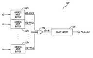
- the asynchronous interface circuit 100includes address input buffers 102 a-n, each receiving a respective input address signal representing one bit of the input address A 0 -An, and further having outputs coupled to inputs of a NOR gate 104 .
- Each of the row address input buffers 102 a-nincludes an address transient detector (ATD) that generates an output pulse ATD_PULSE in response to the respective input address signal making a logic state transition.
- ATDaddress transient detector
- the row address input buffers 102 a-n , and the ATDs included in eachare conventional in design and are known in the art. With the configuration shown in FIG.
- the NOR gate 104when an ATD_PULSE is output by any of the row address input buffers 102 a - 102 n, the NOR gate 104 generates an output pulse ATD_IN that is provided to a delay circuit 106 .
- the delay circuit 106generates an output PULSE_OUT that is used to begin an access operation of the DRAM memory core.
- the asynchronous interface circuit 100can be used with a conventional DRAM memory core to provide an asynchronous pseudo-static SRAM operation.
- a conventional DRAM memory coreis not well suited for the asynchronous nature of a conventional SRAM address interface because random addresses can be asserted without timing restriction.
- a time period after the address is assertedtypically referred to as the address access time, t AA , output data is provided.
- the timing specificationsare violated, and the address changes before the output data is provided, data stored by the SRAM memory core will not be lost because of the manner in which data is stored by conventional SRAM memory cells.
- the asynchronous interface circuit 100can take randomly scheduled address transitions, such as those allowed for conventional SRAM devices, and convert them into scheduled events which can be asserted to a DRAM memory core in an orderly fashion
- FIG. 2illustrates a delay circuit 120 according to an embodiment of the present invention.
- the delay circuit 120can be substituted for the delay circuit 106 shown in FIG. 1 .
- the delay circuit 120includes at least one delay stage 140 .
- Each delay stage 140has a delay input and an ATD input, and further has a delay output.
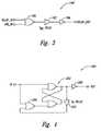
- An embodiment of the delay stage 140is illustrated in FIG. 3 .
- the delay stage 140includes a two-input NOR gate 180 having an output coupled to an input of an inverter 184 through a delay device 182 .
- a first input of the NOR gate 180represents the delay input and a second input represents the ATD input.
- the delay stage 140provides an output signal that is similar to the signal applied to the delay input except that it is delayed by a time t dd of the delay device 182 .
- a first delay stage 140receives the ATD_IN signal at both its delay input and reset input. Subsequent delay stages 140 are coupled such that the delay input is coupled to the delay output of the previous delay stage 140 , as illustrated in FIG. 2 .
- Each delay stage 140generates at its delay output a version of the signal applied to its delay input but delayed by a time delay t dd .
- the ATD input of each of the delay stages 140is coupled to receive the ATD_IN signal.
- the delay output of the last delay stage 140is coupled to a first input of a two-input NOR gate 150 .
- a second input of the NOR gate 150is coupled to receive the ATD_IN signal.
- An output of the NOR gate 150is coupled to a pulse generator 154 through an inverter 152 .
- the pulse generator 154generates a pulse PULSE_OUT in response to the falling edge of signal output by the inverter 152 .
- the PULSE_OUT signalis used to start an access operation to a conventional DRAM memory core.
- the delay circuit 120In operation, the delay circuit 120 generates a PULSE_OUT pulse a time delay t d after the falling edge of the most recent ATD_IN pulse.
- the time delay t dis approximately the sum of the delay of each delay stage 140 .
- any gate delayshave been ignored. However, it will be appreciated that some time will be added to the time delay t d because of the gate delays.
- the delay circuit 120receives an ATD_IN pulse, the output of the inverter 152 goes HIGH and the delay output of each of the delay stages 140 go HIGH t dd after the rising edge of the ATD_IN pulse. On the falling edge of the ATD_IN pulse, the delay circuit begins counting the time delay t d .
- the pulse generator 154then generates a PULSE_OUT pulse that can be used to start an access operation to a DRAM memory core.
- the delay stages 140 of the timing chainare essentially reset because the delay output of each of the delay stages 140 will go HIGH again in response to the new ATD_IN pulse.
- the t d countdownwill begin again in response to the falling edge of the new ATD_IN pulse, as previously described.
- the pulse generator 154will not generate a PULSE_OUT pulse until t d after the falling edge of the last ATD_IN pulse provided to the delay circuit 120 , and consequently, no access operation will be initiated until that time.
- an unrestricted address transition input patterncan be converted by the asynchronous interface circuit 100 ( FIG. 1 ) into scheduled address events suitable for scheduled array accesses of a DRAM memory core. That is, with the asynchronous interface circuit 100 , once a given address is asserted to the DRAM memory core, no new addresses are asserted until the access in progress has completed.
- FIG. 4illustrates a pulse circuit 200 according to an embodiment of the present invention.
- the pulse circuitcan be used to generate an output pulse signal OUT having a minimum pulse width of t w even if the input pulse signal IN has a pulse width less than tw.
- the pulse circuit 200can be used to ensure that the ATD_IN signal provided to the delay circuit 120 ( FIG. 2 ) is of sufficient width to reset the delay stages 140 and prevent the pulse generator 154 from generating a PULSE_OUT signal that will inadvertently initiate an access operation of a DRAM memory core.
- the pulse circuit 200is coupled between the output of the NOR gate 104 ( FIG. 1 ) and the input of the delay circuit 106 .
- the output pulse of the NOR gate 104will provide to the delay circuit 106 a ATD_IN signal of sufficient pulse width to reset the delay circuit 106 . It will be appreciated by those of ordinary skill in the art that the polarity of the signals can be reversed in an alternative implementation of the pulse circuit 200 and remain in the scope of the present invention.
- the pulse circuit 200includes an active HIGH S-R latch 202 formed from two cross-coupled NOR gates.
- the latch 202has a first input coupled to receive the IN signal and a second input coupled to the output of a two-input NOR gate 204 .
- the output of the latch 202is coupled to an inverter 206 , from which the OUT signal is provided.
- the output of the latch 202is also coupled to a first input of the NOR gate 204 through a delay device 208 having a time delay of tw.
- a second input off the NOR gate 204is coupled to receive the IN signal.
- the pulse circuit 200will generate an OUT signal having a pulse width of at least t w from a pulse IN signal, even if the pulse width of the IN signal is less than tw, and no matter how many times the IN signal transitions during the time tw.
- the length of delay time t d for the delay circuit 120can be selected to accommodate various operations related to having a DRAM memory core. For example, as previously mentioned, as is well known in the art, DRAM memory cells need to be periodically refreshed to retain data.
- the delay t d through the delay chain 120can be selected such that a memory array refresh operation can be performed during t d . That is, the time for t d can be matched according to the memory array refresh access time taking into consideration such factors as the impedance and gate delays encountered during the refresh operation.
- t dBy selecting t d in this fashion, a memory array refresh operation that is in progress can be completed, and thus, avoid any potential loss of data, although a new address assertion is made during the operation because actual access to the memory array is not initiated until after the delay time t d has elapsed. By this time, the memory refresh operation would have been completed.
- t dThe selection of t d will determine to some degree the delay time t dd of the delay device 182 ( FIG. 3 ) in each delay stage 140 . It will be appreciated that t d and t dd are related in, a manner that t d is roughly the product of the number of delay stages 140 and t dd . Thus, for a given time t d , fewer delay stages can be used where t dd is made longer. Alternatively, more delay stages could be used where t dd is made shorter. Moreover, although the each delay stage 140 has been described herein as having the same delay time t dd , the delay time of each delay stage can be modified such that more than one common t dd is used without departing from the scope of the present invention.
- t wcan be selected so that a pulse generated by the pulse circuit 200 will ensure that each of the delay stages 140 will be reset, even if the input pulse to the pulse circuit 200 is less than t w .
- the delay stage 140( FIG. 3 ) has been illustrated and described as including a two-input NOR gate 180 .
- a delay stagecould also be implemented using a two-input NAND gate if the polarity of the signals are reversed.
- Other previously described circuitscan be modified in the same manner, as is well known in the art.
- the particular polarity and associated circuitry used in implementing embodiments of the present inventioncan be modified without departing from the scope of the present invention.
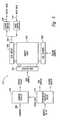
- FIG. 5illustrates a portion of a memory device 500 according to an embodiment of the present invention.
- the memory device 500is an asynchronous pseudostatic SRAM that includes a conventional DRAM memory array 502 .
- the memory device 500includes a command decoder 506 that receives memory commands through a command bus 508 and generates corresponding control signals within the memory device 500 to carry out various memory operations. Row and column address signals are applied to the memory device 500 through an address bus 520 and provided to an asynchronous interface circuit 510 that is in accordance with an embodiment of the present invention.
- the asynchronous interface circuit 510generates a PULSE_OUT pulse to start an access operation to the memory array 502 .
- the PULSE_OUT pulseis provided to the command decoder 506 .
- the PULSE_OUT signalcan be provided to alternative or additional functional blocks of the memory device 500 without departing from the scope of the present invention.
- the row and column addressesare provided by address input buffers (not shown) included in the asynchronous interface circuit 510 for decoding by a row address decoder 524 and a column address decoder 528 , respectively.
- Memory array read/write circuitry 530are coupled to the array 502 to provide read data to a data output buffer 534 via a input-output data bus 540 . Write data are applied to the memory array 502 through a data input buffer 544 and the memory array read/write circuitry 530 .
- the command controller 506responds to memory commands applied to the command bus 508 to perform various operations on the memory array 502 . In particular, the command controller 506 is used to generate internal control signals to read data from and write data to the memory array 502 .
- an address provided on the address bus 520is decoded by the row decoder 524 to access one row of the memory array 502 .
- input provided on the address bus 520is decoded by the column decoder 528 to access at least one column of the memory array 502 .
- the data stored in the addressed memory cell or cellsare then transferred to the output buffer 534 and provided on the data output lines.
- the addressed memory cellis accessed and data provided on the data input lines and the data input buffer 544 is stored in the cell.
- FIG. 6is a block diagram of a computer system 600 including computer circuitry 602 that contains the memory device 500 of FIG. 5 .
- the computer circuitry 602performs various computing functions, such as executing specific software to perform specific calculations or tasks.
- the computer system 600includes one or more input devices 604 , such as a keyboard, coupled to the computer circuitry 602 to allow an operator to interface with the computer system.
- the computer system 600also includes one or more output devices 606 coupled to the computer circuitry 602 , such output devices typically being a display device.
- One or more data storage devices 608are also typically coupled to the computer circuitry 602 to store data or retrieve data. Examples of storage devices 608 include hard disks and non-volatile memory.
- the computer system 600also includes a wireless communication link 610 through which the computer circuitry can send and receive data through a wireless medium.
- the computer circuitry 602is typically coupled to the memory device 500 through appropriate address, data, and control busses to provide for writing data to and reading data from the memory.
Landscapes
- Engineering & Computer Science (AREA)
- Microelectronics & Electronic Packaging (AREA)
- Computer Hardware Design (AREA)
- Dram (AREA)
Abstract
Description
Claims (23)
Priority Applications (1)
| Application Number | Priority Date | Filing Date | Title |
|---|---|---|---|
| US10/754,658US7106637B2 (en) | 2002-03-19 | 2004-01-08 | Asynchronous interface circuit and method for a pseudo-static memory device |
Applications Claiming Priority (2)
| Application Number | Priority Date | Filing Date | Title |
|---|---|---|---|
| US10/102,221US6690606B2 (en) | 2002-03-19 | 2002-03-19 | Asynchronous interface circuit and method for a pseudo-static memory device |
| US10/754,658US7106637B2 (en) | 2002-03-19 | 2004-01-08 | Asynchronous interface circuit and method for a pseudo-static memory device |
Related Parent Applications (1)
| Application Number | Title | Priority Date | Filing Date |
|---|---|---|---|
| US10/102,221ContinuationUS6690606B2 (en) | 2002-03-19 | 2002-03-19 | Asynchronous interface circuit and method for a pseudo-static memory device |
Publications (2)
| Publication Number | Publication Date |
|---|---|
| US20040141397A1 US20040141397A1 (en) | 2004-07-22 |
| US7106637B2true US7106637B2 (en) | 2006-09-12 |
Family
ID=28040157
Family Applications (2)
| Application Number | Title | Priority Date | Filing Date |
|---|---|---|---|
| US10/102,221Expired - LifetimeUS6690606B2 (en) | 2002-03-19 | 2002-03-19 | Asynchronous interface circuit and method for a pseudo-static memory device |
| US10/754,658Expired - LifetimeUS7106637B2 (en) | 2002-03-19 | 2004-01-08 | Asynchronous interface circuit and method for a pseudo-static memory device |
Family Applications Before (1)
| Application Number | Title | Priority Date | Filing Date |
|---|---|---|---|
| US10/102,221Expired - LifetimeUS6690606B2 (en) | 2002-03-19 | 2002-03-19 | Asynchronous interface circuit and method for a pseudo-static memory device |
Country Status (7)
| Country | Link |
|---|---|
| US (2) | US6690606B2 (en) |
| EP (1) | EP1490875A4 (en) |
| JP (1) | JP2005527926A (en) |
| KR (1) | KR20040101329A (en) |
| CN (1) | CN1643610A (en) |
| AU (1) | AU2003214238A1 (en) |
| WO (1) | WO2003081596A1 (en) |
Cited By (3)
| Publication number | Priority date | Publication date | Assignee | Title |
|---|---|---|---|---|
| US20050232034A1 (en)* | 2004-04-19 | 2005-10-20 | Tatung Co., Ltd. | Auxiliary device for operating M-DOC series flash memory and non-X86 system processor in synchronism |
| US7640413B2 (en) | 2003-02-03 | 2009-12-29 | Micron Technology, Inc. | Detection circuit for mixed asynchronous and synchronous memory operation |
| US20120146827A1 (en)* | 2009-08-20 | 2012-06-14 | Rohde & Schwarz Gmbh & Co. Kg | Coding device, device for reprocessing a digital baseband signal or intermediate frequency signal, system and method for external digital coding |
Families Citing this family (9)
| Publication number | Priority date | Publication date | Assignee | Title |
|---|---|---|---|---|
| US6690606B2 (en)* | 2002-03-19 | 2004-02-10 | Micron Technology, Inc. | Asynchronous interface circuit and method for a pseudo-static memory device |
| JP4245317B2 (en)* | 2002-08-28 | 2009-03-25 | Necエレクトロニクス株式会社 | Semiconductor memory device |
| DE10329369B4 (en)* | 2003-06-30 | 2010-01-28 | Qimonda Ag | Circuit and method for refreshing memory cells of a dynamic memory |
| US7167400B2 (en)* | 2004-06-22 | 2007-01-23 | Micron Technology, Inc. | Apparatus and method for improving dynamic refresh in a memory device |
| US7560956B2 (en)* | 2005-08-03 | 2009-07-14 | Micron Technology, Inc. | Method and apparatus for selecting an operating mode based on a determination of the availability of internal clock signals |
| US8347165B2 (en)* | 2007-12-17 | 2013-01-01 | Micron Technology, Inc. | Self-timed error correcting code evaluation system and method |
| DE102008006530B4 (en)* | 2008-01-29 | 2017-10-12 | Continental Automotive Gmbh | Control system and working method for a control system |
| CN112349319B (en)* | 2020-11-09 | 2023-12-29 | 无锡舜铭存储科技有限公司 | Memory read-write control circuit and operation method thereof |
| CN115691609A (en)* | 2022-10-13 | 2023-02-03 | 兰州大学 | Asynchronous storage unit and method based on event-driven circuit design |
Citations (26)
| Publication number | Priority date | Publication date | Assignee | Title |
|---|---|---|---|---|
| US4293926A (en) | 1978-02-13 | 1981-10-06 | Hitachi, Ltd. | Dynamic type semiconductor memory equipment |
| US5258952A (en) | 1990-12-14 | 1993-11-02 | Sgs-Thomson Microelectronics, Inc. | Semiconductor memory with separate time-out control for read and write operations |
| US5374894A (en) | 1992-08-19 | 1994-12-20 | Hyundai Electronics America | Transition detection circuit |
| US5471157A (en) | 1994-03-31 | 1995-11-28 | Sgs-Thomson Microelectronics, Inc. | Integrated circuit with centralized control of edge transition detection pulse generation |
| US5566129A (en) | 1992-02-28 | 1996-10-15 | Sony Corporation | Semiconductor memory device with address transition detector |
| US5600605A (en) | 1995-06-07 | 1997-02-04 | Micron Technology, Inc. | Auto-activate on synchronous dynamic random access memory |
| US5666321A (en) | 1995-09-01 | 1997-09-09 | Micron Technology, Inc. | Synchronous DRAM memory with asynchronous column decode |
| US5802555A (en) | 1995-03-15 | 1998-09-01 | Texas Instruments Incorporated | Computer system including a refresh controller circuit having a row address strobe multiplexer and associated method |
| US5805517A (en) | 1996-12-27 | 1998-09-08 | Intel Corporation | Self-calibrating address transition detection scheme |
| US5835440A (en) | 1997-08-06 | 1998-11-10 | Micron Technology, Inc. | Memory device equilibration circuit and method |
| JPH11238380A (en) | 1998-02-19 | 1999-08-31 | Ricoh Co Ltd | Semiconductor memory circuit |
| US6058070A (en) | 1997-08-29 | 2000-05-02 | Stmicroelectronics S.R.L. | Glitch immune ATD circuitry |
| US6075751A (en) | 1999-01-15 | 2000-06-13 | Intel Corporation | Signal transition detector for asynchronous circuits |
| US6166990A (en) | 1998-11-26 | 2000-12-26 | Mitsubishi Denki Kabushiki Kaisha | Clock reproduction circuit that can reproduce internal clock signal correctly in synchronization with external clock signal |
| US6373303B2 (en) | 2000-05-22 | 2002-04-16 | Kabushiki Kaisha Toshiba | Sync signal generating circuit provided in semiconductor integrated circuit |
| US6396758B2 (en) | 2000-02-29 | 2002-05-28 | Fujitsu Limited | Semiconductor memory device |
| US6507532B1 (en) | 1999-11-30 | 2003-01-14 | Mitsubishi Denki Kabushiki Kaisha | Semiconductor memory device having row-related circuit operating at high speed |
| US6564285B1 (en) | 1994-06-03 | 2003-05-13 | Intel Corporation | Synchronous interface for a nonvolatile memory |
| US6597615B2 (en) | 2000-09-01 | 2003-07-22 | Seiko Epson Corporation | Refresh control for semiconductor memory device |
| US6636449B2 (en) | 2000-04-28 | 2003-10-21 | Fujitsu Limited | Memory circuit with automatic precharge function, and integrated circuit device with automatic internal command function |
| US6658544B2 (en) | 2000-12-27 | 2003-12-02 | Koninklijke Philips Electronics N.V. | Techniques to asynchronously operate a synchronous memory |
| US6675256B1 (en) | 1999-11-19 | 2004-01-06 | Stmicroelectronics S.A. | Fast DRAM control method and adapted controller |
| US6690606B2 (en) | 2002-03-19 | 2004-02-10 | Micron Technology, Inc. | Asynchronous interface circuit and method for a pseudo-static memory device |
| US6701419B2 (en) | 2000-10-18 | 2004-03-02 | Stmicroelectronics S.R.L. | Interlaced memory device with random or sequential access |
| US6714479B2 (en)* | 2000-07-26 | 2004-03-30 | Nec Electronics Corporation | Semiconductor memory and control method |
| US6920524B2 (en) | 2003-02-03 | 2005-07-19 | Micron Technology, Inc. | Detection circuit for mixed asynchronous and synchronous memory operation |
- 2002
- 2002-03-19USUS10/102,221patent/US6690606B2/ennot_activeExpired - Lifetime
- 2003
- 2003-03-19KRKR10-2004-7014819Apatent/KR20040101329A/ennot_activeCeased
- 2003-03-19CNCNA038065428Apatent/CN1643610A/enactivePending
- 2003-03-19EPEP03711647Apatent/EP1490875A4/ennot_activeCeased
- 2003-03-19WOPCT/US2003/008510patent/WO2003081596A1/enactiveApplication Filing
- 2003-03-19JPJP2003579226Apatent/JP2005527926A/enactivePending
- 2003-03-19AUAU2003214238Apatent/AU2003214238A1/ennot_activeAbandoned
- 2004
- 2004-01-08USUS10/754,658patent/US7106637B2/ennot_activeExpired - Lifetime
Patent Citations (26)
| Publication number | Priority date | Publication date | Assignee | Title |
|---|---|---|---|---|
| US4293926A (en) | 1978-02-13 | 1981-10-06 | Hitachi, Ltd. | Dynamic type semiconductor memory equipment |
| US5258952A (en) | 1990-12-14 | 1993-11-02 | Sgs-Thomson Microelectronics, Inc. | Semiconductor memory with separate time-out control for read and write operations |
| US5566129A (en) | 1992-02-28 | 1996-10-15 | Sony Corporation | Semiconductor memory device with address transition detector |
| US5374894A (en) | 1992-08-19 | 1994-12-20 | Hyundai Electronics America | Transition detection circuit |
| US5471157A (en) | 1994-03-31 | 1995-11-28 | Sgs-Thomson Microelectronics, Inc. | Integrated circuit with centralized control of edge transition detection pulse generation |
| US6564285B1 (en) | 1994-06-03 | 2003-05-13 | Intel Corporation | Synchronous interface for a nonvolatile memory |
| US5802555A (en) | 1995-03-15 | 1998-09-01 | Texas Instruments Incorporated | Computer system including a refresh controller circuit having a row address strobe multiplexer and associated method |
| US5600605A (en) | 1995-06-07 | 1997-02-04 | Micron Technology, Inc. | Auto-activate on synchronous dynamic random access memory |
| US5666321A (en) | 1995-09-01 | 1997-09-09 | Micron Technology, Inc. | Synchronous DRAM memory with asynchronous column decode |
| US5805517A (en) | 1996-12-27 | 1998-09-08 | Intel Corporation | Self-calibrating address transition detection scheme |
| US5835440A (en) | 1997-08-06 | 1998-11-10 | Micron Technology, Inc. | Memory device equilibration circuit and method |
| US6058070A (en) | 1997-08-29 | 2000-05-02 | Stmicroelectronics S.R.L. | Glitch immune ATD circuitry |
| JPH11238380A (en) | 1998-02-19 | 1999-08-31 | Ricoh Co Ltd | Semiconductor memory circuit |
| US6166990A (en) | 1998-11-26 | 2000-12-26 | Mitsubishi Denki Kabushiki Kaisha | Clock reproduction circuit that can reproduce internal clock signal correctly in synchronization with external clock signal |
| US6075751A (en) | 1999-01-15 | 2000-06-13 | Intel Corporation | Signal transition detector for asynchronous circuits |
| US6675256B1 (en) | 1999-11-19 | 2004-01-06 | Stmicroelectronics S.A. | Fast DRAM control method and adapted controller |
| US6507532B1 (en) | 1999-11-30 | 2003-01-14 | Mitsubishi Denki Kabushiki Kaisha | Semiconductor memory device having row-related circuit operating at high speed |
| US6396758B2 (en) | 2000-02-29 | 2002-05-28 | Fujitsu Limited | Semiconductor memory device |
| US6636449B2 (en) | 2000-04-28 | 2003-10-21 | Fujitsu Limited | Memory circuit with automatic precharge function, and integrated circuit device with automatic internal command function |
| US6373303B2 (en) | 2000-05-22 | 2002-04-16 | Kabushiki Kaisha Toshiba | Sync signal generating circuit provided in semiconductor integrated circuit |
| US6714479B2 (en)* | 2000-07-26 | 2004-03-30 | Nec Electronics Corporation | Semiconductor memory and control method |
| US6597615B2 (en) | 2000-09-01 | 2003-07-22 | Seiko Epson Corporation | Refresh control for semiconductor memory device |
| US6701419B2 (en) | 2000-10-18 | 2004-03-02 | Stmicroelectronics S.R.L. | Interlaced memory device with random or sequential access |
| US6658544B2 (en) | 2000-12-27 | 2003-12-02 | Koninklijke Philips Electronics N.V. | Techniques to asynchronously operate a synchronous memory |
| US6690606B2 (en) | 2002-03-19 | 2004-02-10 | Micron Technology, Inc. | Asynchronous interface circuit and method for a pseudo-static memory device |
| US6920524B2 (en) | 2003-02-03 | 2005-07-19 | Micron Technology, Inc. | Detection circuit for mixed asynchronous and synchronous memory operation |
Non-Patent Citations (2)
| Title |
|---|
| "1.8 Volt Intel(R) Wireless Flash Memory (W18)," Datasheet, Intel Corporation, Jan. 2003, pp. 1-102. |
| "Intel(R) 1.8 Volt Wireless Flash Memory (W18/W30)," Product Brief Flash Products Group, Intel Corporation, 2002, pp. 1-2. |
Cited By (7)
| Publication number | Priority date | Publication date | Assignee | Title |
|---|---|---|---|---|
| US7640413B2 (en) | 2003-02-03 | 2009-12-29 | Micron Technology, Inc. | Detection circuit for mixed asynchronous and synchronous memory operation |
| US20100088483A1 (en)* | 2003-02-03 | 2010-04-08 | Micron Technology, Inc. | Detection circuit for mixed asynchronous and synchronous memory operation |
| US8082413B2 (en) | 2003-02-03 | 2011-12-20 | Micron Technology, Inc. | Detection circuit for mixed asynchronous and synchronous memory operation |
| US9772969B2 (en) | 2003-02-03 | 2017-09-26 | Micron Technology, Inc. | Detection circuit for mixed asynchronous and synchronous memory operation |
| US20050232034A1 (en)* | 2004-04-19 | 2005-10-20 | Tatung Co., Ltd. | Auxiliary device for operating M-DOC series flash memory and non-X86 system processor in synchronism |
| US20120146827A1 (en)* | 2009-08-20 | 2012-06-14 | Rohde & Schwarz Gmbh & Co. Kg | Coding device, device for reprocessing a digital baseband signal or intermediate frequency signal, system and method for external digital coding |
| US8692698B2 (en)* | 2009-08-20 | 2014-04-08 | Rohde & Schwarz Gmbh & Co. Kg | Coding device, device for reprocessing a digital baseband signal or intermediate frequency signal, system and method for external digital coding |
Also Published As
| Publication number | Publication date |
|---|---|
| EP1490875A1 (en) | 2004-12-29 |
| KR20040101329A (en) | 2004-12-02 |
| CN1643610A (en) | 2005-07-20 |
| US20040141397A1 (en) | 2004-07-22 |
| US6690606B2 (en) | 2004-02-10 |
| US20030179612A1 (en) | 2003-09-25 |
| AU2003214238A1 (en) | 2003-10-08 |
| EP1490875A4 (en) | 2006-02-08 |
| WO2003081596A1 (en) | 2003-10-02 |
| JP2005527926A (en) | 2005-09-15 |
Similar Documents
| Publication | Publication Date | Title |
|---|---|---|
| US7640413B2 (en) | Detection circuit for mixed asynchronous and synchronous memory operation | |
| US5490114A (en) | High performance extended data out | |
| US6809979B1 (en) | Complete refresh scheme for 3T dynamic random access memory cells | |
| US6826104B2 (en) | Synchronous semiconductor memory | |
| KR101257366B1 (en) | Semiconductor memory device and refresh control method thereof | |
| US7106637B2 (en) | Asynchronous interface circuit and method for a pseudo-static memory device | |
| JPH01125795A (en) | Virtual type static semiconductor memory device | |
| US6735139B2 (en) | System and method for providing asynchronous SRAM functionality with a DRAM array | |
| US7254090B2 (en) | Semiconductor memory device | |
| JP4463680B2 (en) | Semiconductor memory word line latch | |
| US7583541B2 (en) | Asynchronous semiconductor memory | |
| JP4241087B2 (en) | Semiconductor memory device | |
| JP2001243764A (en) | Semiconductor storage device | |
| JP4386657B2 (en) | Semiconductor memory device | |
| JP4143515B2 (en) | Semiconductor memory device | |
| JP5256879B2 (en) | Semiconductor memory device | |
| JPS60254260A (en) | semiconductor storage device |
Legal Events
| Date | Code | Title | Description |
|---|---|---|---|
| FEPP | Fee payment procedure | Free format text:PAYOR NUMBER ASSIGNED (ORIGINAL EVENT CODE: ASPN); ENTITY STATUS OF PATENT OWNER: LARGE ENTITY | |
| STCF | Information on status: patent grant | Free format text:PATENTED CASE | |
| FPAY | Fee payment | Year of fee payment:4 | |
| FPAY | Fee payment | Year of fee payment:8 | |
| AS | Assignment | Owner name:U.S. BANK NATIONAL ASSOCIATION, AS COLLATERAL AGENT, CALIFORNIA Free format text:SECURITY INTEREST;ASSIGNOR:MICRON TECHNOLOGY, INC.;REEL/FRAME:038669/0001 Effective date:20160426 Owner name:U.S. BANK NATIONAL ASSOCIATION, AS COLLATERAL AGEN Free format text:SECURITY INTEREST;ASSIGNOR:MICRON TECHNOLOGY, INC.;REEL/FRAME:038669/0001 Effective date:20160426 | |
| AS | Assignment | Owner name:MORGAN STANLEY SENIOR FUNDING, INC., AS COLLATERAL AGENT, MARYLAND Free format text:PATENT SECURITY AGREEMENT;ASSIGNOR:MICRON TECHNOLOGY, INC.;REEL/FRAME:038954/0001 Effective date:20160426 Owner name:MORGAN STANLEY SENIOR FUNDING, INC., AS COLLATERAL Free format text:PATENT SECURITY AGREEMENT;ASSIGNOR:MICRON TECHNOLOGY, INC.;REEL/FRAME:038954/0001 Effective date:20160426 | |
| AS | Assignment | Owner name:U.S. BANK NATIONAL ASSOCIATION, AS COLLATERAL AGENT, CALIFORNIA Free format text:CORRECTIVE ASSIGNMENT TO CORRECT THE REPLACE ERRONEOUSLY FILED PATENT #7358718 WITH THE CORRECT PATENT #7358178 PREVIOUSLY RECORDED ON REEL 038669 FRAME 0001. ASSIGNOR(S) HEREBY CONFIRMS THE SECURITY INTEREST;ASSIGNOR:MICRON TECHNOLOGY, INC.;REEL/FRAME:043079/0001 Effective date:20160426 Owner name:U.S. BANK NATIONAL ASSOCIATION, AS COLLATERAL AGEN Free format text:CORRECTIVE ASSIGNMENT TO CORRECT THE REPLACE ERRONEOUSLY FILED PATENT #7358718 WITH THE CORRECT PATENT #7358178 PREVIOUSLY RECORDED ON REEL 038669 FRAME 0001. ASSIGNOR(S) HEREBY CONFIRMS THE SECURITY INTEREST;ASSIGNOR:MICRON TECHNOLOGY, INC.;REEL/FRAME:043079/0001 Effective date:20160426 | |
| MAFP | Maintenance fee payment | Free format text:PAYMENT OF MAINTENANCE FEE, 12TH YEAR, LARGE ENTITY (ORIGINAL EVENT CODE: M1553) Year of fee payment:12 | |
| AS | Assignment | Owner name:JPMORGAN CHASE BANK, N.A., AS COLLATERAL AGENT, ILLINOIS Free format text:SECURITY INTEREST;ASSIGNORS:MICRON TECHNOLOGY, INC.;MICRON SEMICONDUCTOR PRODUCTS, INC.;REEL/FRAME:047540/0001 Effective date:20180703 Owner name:JPMORGAN CHASE BANK, N.A., AS COLLATERAL AGENT, IL Free format text:SECURITY INTEREST;ASSIGNORS:MICRON TECHNOLOGY, INC.;MICRON SEMICONDUCTOR PRODUCTS, INC.;REEL/FRAME:047540/0001 Effective date:20180703 | |
| AS | Assignment | Owner name:MICRON TECHNOLOGY, INC., IDAHO Free format text:RELEASE BY SECURED PARTY;ASSIGNOR:U.S. BANK NATIONAL ASSOCIATION, AS COLLATERAL AGENT;REEL/FRAME:047243/0001 Effective date:20180629 | |
| AS | Assignment | Owner name:MICRON TECHNOLOGY, INC., IDAHO Free format text:RELEASE BY SECURED PARTY;ASSIGNOR:MORGAN STANLEY SENIOR FUNDING, INC., AS COLLATERAL AGENT;REEL/FRAME:050937/0001 Effective date:20190731 | |
| AS | Assignment | Owner name:MICRON SEMICONDUCTOR PRODUCTS, INC., IDAHO Free format text:RELEASE BY SECURED PARTY;ASSIGNOR:JPMORGAN CHASE BANK, N.A., AS COLLATERAL AGENT;REEL/FRAME:051028/0001 Effective date:20190731 Owner name:MICRON TECHNOLOGY, INC., IDAHO Free format text:RELEASE BY SECURED PARTY;ASSIGNOR:JPMORGAN CHASE BANK, N.A., AS COLLATERAL AGENT;REEL/FRAME:051028/0001 Effective date:20190731 |