US7106296B1 - Electronic book with multiple page displays - Google Patents
Electronic book with multiple page displaysDownload PDFInfo
- Publication number
- US7106296B1 US7106296B1US08/983,404US98340499AUS7106296B1US 7106296 B1US7106296 B1US 7106296B1US 98340499 AUS98340499 AUS 98340499AUS 7106296 B1US7106296 B1US 7106296B1
- Authority
- US
- United States
- Prior art keywords
- page
- address
- lines
- column
- display
- Prior art date
- Legal status (The legal status is an assumption and is not a legal conclusion. Google has not performed a legal analysis and makes no representation as to the accuracy of the status listed.)
- Expired - Fee Related
Links
Images


Classifications
- B—PERFORMING OPERATIONS; TRANSPORTING
- B41—PRINTING; LINING MACHINES; TYPEWRITERS; STAMPS
- B41J—TYPEWRITERS; SELECTIVE PRINTING MECHANISMS, i.e. MECHANISMS PRINTING OTHERWISE THAN FROM A FORME; CORRECTION OF TYPOGRAPHICAL ERRORS
- B41J2/00—Typewriters or selective printing mechanisms characterised by the printing or marking process for which they are designed
- B41J2/005—Typewriters or selective printing mechanisms characterised by the printing or marking process for which they are designed characterised by bringing liquid or particles selectively into contact with a printing material
- B41J2/01—Ink jet
- B41J2/015—Ink jet characterised by the jet generation process
- B41J2/02—Ink jet characterised by the jet generation process generating a continuous ink jet
- B—PERFORMING OPERATIONS; TRANSPORTING
- B41—PRINTING; LINING MACHINES; TYPEWRITERS; STAMPS
- B41J—TYPEWRITERS; SELECTIVE PRINTING MECHANISMS, i.e. MECHANISMS PRINTING OTHERWISE THAN FROM A FORME; CORRECTION OF TYPOGRAPHICAL ERRORS
- B41J3/00—Typewriters or selective printing or marking mechanisms characterised by the purpose for which they are constructed
- B41J3/407—Typewriters or selective printing or marking mechanisms characterised by the purpose for which they are constructed for marking on special material
- B41J3/4076—Typewriters or selective printing or marking mechanisms characterised by the purpose for which they are constructed for marking on special material printing on rewritable, bistable "electronic paper" by a focused electric or magnetic field
- B—PERFORMING OPERATIONS; TRANSPORTING
- B82—NANOTECHNOLOGY
- B82Y—SPECIFIC USES OR APPLICATIONS OF NANOSTRUCTURES; MEASUREMENT OR ANALYSIS OF NANOSTRUCTURES; MANUFACTURE OR TREATMENT OF NANOSTRUCTURES
- B82Y10/00—Nanotechnology for information processing, storage or transmission, e.g. quantum computing or single electron logic
- B—PERFORMING OPERATIONS; TRANSPORTING
- B82—NANOTECHNOLOGY
- B82Y—SPECIFIC USES OR APPLICATIONS OF NANOSTRUCTURES; MEASUREMENT OR ANALYSIS OF NANOSTRUCTURES; MANUFACTURE OR TREATMENT OF NANOSTRUCTURES
- B82Y20/00—Nanooptics, e.g. quantum optics or photonic crystals
- C—CHEMISTRY; METALLURGY
- C09—DYES; PAINTS; POLISHES; NATURAL RESINS; ADHESIVES; COMPOSITIONS NOT OTHERWISE PROVIDED FOR; APPLICATIONS OF MATERIALS NOT OTHERWISE PROVIDED FOR
- C09D—COATING COMPOSITIONS, e.g. PAINTS, VARNISHES OR LACQUERS; FILLING PASTES; CHEMICAL PAINT OR INK REMOVERS; INKS; CORRECTING FLUIDS; WOODSTAINS; PASTES OR SOLIDS FOR COLOURING OR PRINTING; USE OF MATERIALS THEREFOR
- C09D11/00—Inks
- C09D11/30—Inkjet printing inks
- C—CHEMISTRY; METALLURGY
- C09—DYES; PAINTS; POLISHES; NATURAL RESINS; ADHESIVES; COMPOSITIONS NOT OTHERWISE PROVIDED FOR; APPLICATIONS OF MATERIALS NOT OTHERWISE PROVIDED FOR
- C09D—COATING COMPOSITIONS, e.g. PAINTS, VARNISHES OR LACQUERS; FILLING PASTES; CHEMICAL PAINT OR INK REMOVERS; INKS; CORRECTING FLUIDS; WOODSTAINS; PASTES OR SOLIDS FOR COLOURING OR PRINTING; USE OF MATERIALS THEREFOR
- C09D11/00—Inks
- C09D11/50—Sympathetic, colour changing or similar inks
- G—PHYSICS
- G02—OPTICS
- G02B—OPTICAL ELEMENTS, SYSTEMS OR APPARATUS
- G02B26/00—Optical devices or arrangements for the control of light using movable or deformable optical elements
- G02B26/02—Optical devices or arrangements for the control of light using movable or deformable optical elements for controlling the intensity of light
- G02B26/026—Optical devices or arrangements for the control of light using movable or deformable optical elements for controlling the intensity of light based on the rotation of particles under the influence of an external field, e.g. gyricons, twisting ball displays
- G—PHYSICS
- G02—OPTICS
- G02F—OPTICAL DEVICES OR ARRANGEMENTS FOR THE CONTROL OF LIGHT BY MODIFICATION OF THE OPTICAL PROPERTIES OF THE MEDIA OF THE ELEMENTS INVOLVED THEREIN; NON-LINEAR OPTICS; FREQUENCY-CHANGING OF LIGHT; OPTICAL LOGIC ELEMENTS; OPTICAL ANALOGUE/DIGITAL CONVERTERS
- G02F1/00—Devices or arrangements for the control of the intensity, colour, phase, polarisation or direction of light arriving from an independent light source, e.g. switching, gating or modulating; Non-linear optics
- G02F1/01—Devices or arrangements for the control of the intensity, colour, phase, polarisation or direction of light arriving from an independent light source, e.g. switching, gating or modulating; Non-linear optics for the control of the intensity, phase, polarisation or colour
- G02F1/13—Devices or arrangements for the control of the intensity, colour, phase, polarisation or direction of light arriving from an independent light source, e.g. switching, gating or modulating; Non-linear optics for the control of the intensity, phase, polarisation or colour based on liquid crystals, e.g. single liquid crystal display cells
- G02F1/133—Constructional arrangements; Operation of liquid crystal cells; Circuit arrangements
- G02F1/1333—Constructional arrangements; Manufacturing methods
- G02F1/1334—Constructional arrangements; Manufacturing methods based on polymer dispersed liquid crystals, e.g. microencapsulated liquid crystals
- G—PHYSICS
- G02—OPTICS
- G02F—OPTICAL DEVICES OR ARRANGEMENTS FOR THE CONTROL OF LIGHT BY MODIFICATION OF THE OPTICAL PROPERTIES OF THE MEDIA OF THE ELEMENTS INVOLVED THEREIN; NON-LINEAR OPTICS; FREQUENCY-CHANGING OF LIGHT; OPTICAL LOGIC ELEMENTS; OPTICAL ANALOGUE/DIGITAL CONVERTERS
- G02F1/00—Devices or arrangements for the control of the intensity, colour, phase, polarisation or direction of light arriving from an independent light source, e.g. switching, gating or modulating; Non-linear optics
- G02F1/01—Devices or arrangements for the control of the intensity, colour, phase, polarisation or direction of light arriving from an independent light source, e.g. switching, gating or modulating; Non-linear optics for the control of the intensity, phase, polarisation or colour
- G02F1/13—Devices or arrangements for the control of the intensity, colour, phase, polarisation or direction of light arriving from an independent light source, e.g. switching, gating or modulating; Non-linear optics for the control of the intensity, phase, polarisation or colour based on liquid crystals, e.g. single liquid crystal display cells
- G02F1/133—Constructional arrangements; Operation of liquid crystal cells; Circuit arrangements
- G02F1/1333—Constructional arrangements; Manufacturing methods
- G02F1/1343—Electrodes
- G02F1/134309—Electrodes characterised by their geometrical arrangement
- G—PHYSICS
- G02—OPTICS
- G02F—OPTICAL DEVICES OR ARRANGEMENTS FOR THE CONTROL OF LIGHT BY MODIFICATION OF THE OPTICAL PROPERTIES OF THE MEDIA OF THE ELEMENTS INVOLVED THEREIN; NON-LINEAR OPTICS; FREQUENCY-CHANGING OF LIGHT; OPTICAL LOGIC ELEMENTS; OPTICAL ANALOGUE/DIGITAL CONVERTERS
- G02F1/00—Devices or arrangements for the control of the intensity, colour, phase, polarisation or direction of light arriving from an independent light source, e.g. switching, gating or modulating; Non-linear optics
- G02F1/01—Devices or arrangements for the control of the intensity, colour, phase, polarisation or direction of light arriving from an independent light source, e.g. switching, gating or modulating; Non-linear optics for the control of the intensity, phase, polarisation or colour
- G02F1/13—Devices or arrangements for the control of the intensity, colour, phase, polarisation or direction of light arriving from an independent light source, e.g. switching, gating or modulating; Non-linear optics for the control of the intensity, phase, polarisation or colour based on liquid crystals, e.g. single liquid crystal display cells
- G02F1/133—Constructional arrangements; Operation of liquid crystal cells; Circuit arrangements
- G02F1/1333—Constructional arrangements; Manufacturing methods
- G02F1/1345—Conductors connecting electrodes to cell terminals
- G—PHYSICS
- G02—OPTICS
- G02F—OPTICAL DEVICES OR ARRANGEMENTS FOR THE CONTROL OF LIGHT BY MODIFICATION OF THE OPTICAL PROPERTIES OF THE MEDIA OF THE ELEMENTS INVOLVED THEREIN; NON-LINEAR OPTICS; FREQUENCY-CHANGING OF LIGHT; OPTICAL LOGIC ELEMENTS; OPTICAL ANALOGUE/DIGITAL CONVERTERS
- G02F1/00—Devices or arrangements for the control of the intensity, colour, phase, polarisation or direction of light arriving from an independent light source, e.g. switching, gating or modulating; Non-linear optics
- G02F1/01—Devices or arrangements for the control of the intensity, colour, phase, polarisation or direction of light arriving from an independent light source, e.g. switching, gating or modulating; Non-linear optics for the control of the intensity, phase, polarisation or colour
- G02F1/13—Devices or arrangements for the control of the intensity, colour, phase, polarisation or direction of light arriving from an independent light source, e.g. switching, gating or modulating; Non-linear optics for the control of the intensity, phase, polarisation or colour based on liquid crystals, e.g. single liquid crystal display cells
- G02F1/133—Constructional arrangements; Operation of liquid crystal cells; Circuit arrangements
- G02F1/135—Liquid crystal cells structurally associated with a photoconducting or a ferro-electric layer, the properties of which can be optically or electrically varied
- G—PHYSICS
- G02—OPTICS
- G02F—OPTICAL DEVICES OR ARRANGEMENTS FOR THE CONTROL OF LIGHT BY MODIFICATION OF THE OPTICAL PROPERTIES OF THE MEDIA OF THE ELEMENTS INVOLVED THEREIN; NON-LINEAR OPTICS; FREQUENCY-CHANGING OF LIGHT; OPTICAL LOGIC ELEMENTS; OPTICAL ANALOGUE/DIGITAL CONVERTERS
- G02F1/00—Devices or arrangements for the control of the intensity, colour, phase, polarisation or direction of light arriving from an independent light source, e.g. switching, gating or modulating; Non-linear optics
- G02F1/01—Devices or arrangements for the control of the intensity, colour, phase, polarisation or direction of light arriving from an independent light source, e.g. switching, gating or modulating; Non-linear optics for the control of the intensity, phase, polarisation or colour
- G02F1/165—Devices or arrangements for the control of the intensity, colour, phase, polarisation or direction of light arriving from an independent light source, e.g. switching, gating or modulating; Non-linear optics for the control of the intensity, phase, polarisation or colour based on translational movement of particles in a fluid under the influence of an applied field
- G02F1/166—Devices or arrangements for the control of the intensity, colour, phase, polarisation or direction of light arriving from an independent light source, e.g. switching, gating or modulating; Non-linear optics for the control of the intensity, phase, polarisation or colour based on translational movement of particles in a fluid under the influence of an applied field characterised by the electro-optical or magneto-optical effect
- G02F1/167—Devices or arrangements for the control of the intensity, colour, phase, polarisation or direction of light arriving from an independent light source, e.g. switching, gating or modulating; Non-linear optics for the control of the intensity, phase, polarisation or colour based on translational movement of particles in a fluid under the influence of an applied field characterised by the electro-optical or magneto-optical effect by electrophoresis
- G—PHYSICS
- G02—OPTICS
- G02F—OPTICAL DEVICES OR ARRANGEMENTS FOR THE CONTROL OF LIGHT BY MODIFICATION OF THE OPTICAL PROPERTIES OF THE MEDIA OF THE ELEMENTS INVOLVED THEREIN; NON-LINEAR OPTICS; FREQUENCY-CHANGING OF LIGHT; OPTICAL LOGIC ELEMENTS; OPTICAL ANALOGUE/DIGITAL CONVERTERS
- G02F1/00—Devices or arrangements for the control of the intensity, colour, phase, polarisation or direction of light arriving from an independent light source, e.g. switching, gating or modulating; Non-linear optics
- G02F1/01—Devices or arrangements for the control of the intensity, colour, phase, polarisation or direction of light arriving from an independent light source, e.g. switching, gating or modulating; Non-linear optics for the control of the intensity, phase, polarisation or colour
- G02F1/165—Devices or arrangements for the control of the intensity, colour, phase, polarisation or direction of light arriving from an independent light source, e.g. switching, gating or modulating; Non-linear optics for the control of the intensity, phase, polarisation or colour based on translational movement of particles in a fluid under the influence of an applied field
- G02F1/1675—Constructional details
- G02F1/16757—Microcapsules
- G—PHYSICS
- G02—OPTICS
- G02F—OPTICAL DEVICES OR ARRANGEMENTS FOR THE CONTROL OF LIGHT BY MODIFICATION OF THE OPTICAL PROPERTIES OF THE MEDIA OF THE ELEMENTS INVOLVED THEREIN; NON-LINEAR OPTICS; FREQUENCY-CHANGING OF LIGHT; OPTICAL LOGIC ELEMENTS; OPTICAL ANALOGUE/DIGITAL CONVERTERS
- G02F1/00—Devices or arrangements for the control of the intensity, colour, phase, polarisation or direction of light arriving from an independent light source, e.g. switching, gating or modulating; Non-linear optics
- G02F1/01—Devices or arrangements for the control of the intensity, colour, phase, polarisation or direction of light arriving from an independent light source, e.g. switching, gating or modulating; Non-linear optics for the control of the intensity, phase, polarisation or colour
- G02F1/165—Devices or arrangements for the control of the intensity, colour, phase, polarisation or direction of light arriving from an independent light source, e.g. switching, gating or modulating; Non-linear optics for the control of the intensity, phase, polarisation or colour based on translational movement of particles in a fluid under the influence of an applied field
- G02F1/1675—Constructional details
- G02F1/1677—Structural association of cells with optical devices, e.g. reflectors or illuminating devices
- G—PHYSICS
- G02—OPTICS
- G02F—OPTICAL DEVICES OR ARRANGEMENTS FOR THE CONTROL OF LIGHT BY MODIFICATION OF THE OPTICAL PROPERTIES OF THE MEDIA OF THE ELEMENTS INVOLVED THEREIN; NON-LINEAR OPTICS; FREQUENCY-CHANGING OF LIGHT; OPTICAL LOGIC ELEMENTS; OPTICAL ANALOGUE/DIGITAL CONVERTERS
- G02F1/00—Devices or arrangements for the control of the intensity, colour, phase, polarisation or direction of light arriving from an independent light source, e.g. switching, gating or modulating; Non-linear optics
- G02F1/01—Devices or arrangements for the control of the intensity, colour, phase, polarisation or direction of light arriving from an independent light source, e.g. switching, gating or modulating; Non-linear optics for the control of the intensity, phase, polarisation or colour
- G02F1/17—Devices or arrangements for the control of the intensity, colour, phase, polarisation or direction of light arriving from an independent light source, e.g. switching, gating or modulating; Non-linear optics for the control of the intensity, phase, polarisation or colour based on variable-absorption elements not provided for in groups G02F1/015 - G02F1/169
- G02F1/172—Devices or arrangements for the control of the intensity, colour, phase, polarisation or direction of light arriving from an independent light source, e.g. switching, gating or modulating; Non-linear optics for the control of the intensity, phase, polarisation or colour based on variable-absorption elements not provided for in groups G02F1/015 - G02F1/169 based on a suspension of orientable dipolar particles, e.g. suspended particles displays
- G—PHYSICS
- G04—HOROLOGY
- G04B—MECHANICALLY-DRIVEN CLOCKS OR WATCHES; MECHANICAL PARTS OF CLOCKS OR WATCHES IN GENERAL; TIME PIECES USING THE POSITION OF THE SUN, MOON OR STARS
- G04B47/00—Time-pieces combined with other articles which do not interfere with the running or the time-keeping of the time-piece
- G—PHYSICS
- G06—COMPUTING OR CALCULATING; COUNTING
- G06F—ELECTRIC DIGITAL DATA PROCESSING
- G06F15/00—Digital computers in general; Data processing equipment in general
- G06F15/02—Digital computers in general; Data processing equipment in general manually operated with input through keyboard and computation using a built-in program, e.g. pocket calculators
- G06F15/025—Digital computers in general; Data processing equipment in general manually operated with input through keyboard and computation using a built-in program, e.g. pocket calculators adapted to a specific application
- G06F15/0283—Digital computers in general; Data processing equipment in general manually operated with input through keyboard and computation using a built-in program, e.g. pocket calculators adapted to a specific application for data storage and retrieval
- G—PHYSICS
- G06—COMPUTING OR CALCULATING; COUNTING
- G06K—GRAPHICAL DATA READING; PRESENTATION OF DATA; RECORD CARRIERS; HANDLING RECORD CARRIERS
- G06K19/00—Record carriers for use with machines and with at least a part designed to carry digital markings
- G06K19/06—Record carriers for use with machines and with at least a part designed to carry digital markings characterised by the kind of the digital marking, e.g. shape, nature, code
- G06K19/067—Record carriers with conductive marks, printed circuits or semiconductor circuit elements, e.g. credit or identity cards also with resonating or responding marks without active components
- G06K19/07—Record carriers with conductive marks, printed circuits or semiconductor circuit elements, e.g. credit or identity cards also with resonating or responding marks without active components with integrated circuit chips
- G06K19/077—Constructional details, e.g. mounting of circuits in the carrier
- G06K19/07701—Constructional details, e.g. mounting of circuits in the carrier the record carrier comprising an interface suitable for human interaction
- G06K19/07703—Constructional details, e.g. mounting of circuits in the carrier the record carrier comprising an interface suitable for human interaction the interface being visual
- G—PHYSICS
- G09—EDUCATION; CRYPTOGRAPHY; DISPLAY; ADVERTISING; SEALS
- G09F—DISPLAYING; ADVERTISING; SIGNS; LABELS OR NAME-PLATES; SEALS
- G09F9/00—Indicating arrangements for variable information in which the information is built-up on a support by selection or combination of individual elements
- G09F9/30—Indicating arrangements for variable information in which the information is built-up on a support by selection or combination of individual elements in which the desired character or characters are formed by combining individual elements
- G09F9/302—Indicating arrangements for variable information in which the information is built-up on a support by selection or combination of individual elements in which the desired character or characters are formed by combining individual elements characterised by the form or geometrical disposition of the individual elements
- G—PHYSICS
- G09—EDUCATION; CRYPTOGRAPHY; DISPLAY; ADVERTISING; SEALS
- G09F—DISPLAYING; ADVERTISING; SIGNS; LABELS OR NAME-PLATES; SEALS
- G09F9/00—Indicating arrangements for variable information in which the information is built-up on a support by selection or combination of individual elements
- G09F9/30—Indicating arrangements for variable information in which the information is built-up on a support by selection or combination of individual elements in which the desired character or characters are formed by combining individual elements
- G09F9/37—Indicating arrangements for variable information in which the information is built-up on a support by selection or combination of individual elements in which the desired character or characters are formed by combining individual elements being movable elements
- G09F9/372—Indicating arrangements for variable information in which the information is built-up on a support by selection or combination of individual elements in which the desired character or characters are formed by combining individual elements being movable elements the positions of the elements being controlled by the application of an electric field
- H—ELECTRICITY
- H10—SEMICONDUCTOR DEVICES; ELECTRIC SOLID-STATE DEVICES NOT OTHERWISE PROVIDED FOR
- H10D—INORGANIC ELECTRIC SEMICONDUCTOR DEVICES
- H10D86/00—Integrated devices formed in or on insulating or conducting substrates, e.g. formed in silicon-on-insulator [SOI] substrates or on stainless steel or glass substrates
- H—ELECTRICITY
- H10—SEMICONDUCTOR DEVICES; ELECTRIC SOLID-STATE DEVICES NOT OTHERWISE PROVIDED FOR
- H10K—ORGANIC ELECTRIC SOLID-STATE DEVICES
- H10K19/00—Integrated devices, or assemblies of multiple devices, comprising at least one organic element specially adapted for rectifying, amplifying, oscillating or switching, covered by group H10K10/00
- G—PHYSICS
- G02—OPTICS
- G02F—OPTICAL DEVICES OR ARRANGEMENTS FOR THE CONTROL OF LIGHT BY MODIFICATION OF THE OPTICAL PROPERTIES OF THE MEDIA OF THE ELEMENTS INVOLVED THEREIN; NON-LINEAR OPTICS; FREQUENCY-CHANGING OF LIGHT; OPTICAL LOGIC ELEMENTS; OPTICAL ANALOGUE/DIGITAL CONVERTERS
- G02F1/00—Devices or arrangements for the control of the intensity, colour, phase, polarisation or direction of light arriving from an independent light source, e.g. switching, gating or modulating; Non-linear optics
- G02F1/01—Devices or arrangements for the control of the intensity, colour, phase, polarisation or direction of light arriving from an independent light source, e.g. switching, gating or modulating; Non-linear optics for the control of the intensity, phase, polarisation or colour
- G02F1/13—Devices or arrangements for the control of the intensity, colour, phase, polarisation or direction of light arriving from an independent light source, e.g. switching, gating or modulating; Non-linear optics for the control of the intensity, phase, polarisation or colour based on liquid crystals, e.g. single liquid crystal display cells
- G02F1/133—Constructional arrangements; Operation of liquid crystal cells; Circuit arrangements
- G02F1/1333—Constructional arrangements; Manufacturing methods
- G02F1/133305—Flexible substrates, e.g. plastics, organic film
- G—PHYSICS
- G02—OPTICS
- G02F—OPTICAL DEVICES OR ARRANGEMENTS FOR THE CONTROL OF LIGHT BY MODIFICATION OF THE OPTICAL PROPERTIES OF THE MEDIA OF THE ELEMENTS INVOLVED THEREIN; NON-LINEAR OPTICS; FREQUENCY-CHANGING OF LIGHT; OPTICAL LOGIC ELEMENTS; OPTICAL ANALOGUE/DIGITAL CONVERTERS
- G02F1/00—Devices or arrangements for the control of the intensity, colour, phase, polarisation or direction of light arriving from an independent light source, e.g. switching, gating or modulating; Non-linear optics
- G02F1/01—Devices or arrangements for the control of the intensity, colour, phase, polarisation or direction of light arriving from an independent light source, e.g. switching, gating or modulating; Non-linear optics for the control of the intensity, phase, polarisation or colour
- G02F1/13—Devices or arrangements for the control of the intensity, colour, phase, polarisation or direction of light arriving from an independent light source, e.g. switching, gating or modulating; Non-linear optics for the control of the intensity, phase, polarisation or colour based on liquid crystals, e.g. single liquid crystal display cells
- G02F1/133—Constructional arrangements; Operation of liquid crystal cells; Circuit arrangements
- G02F1/1333—Constructional arrangements; Manufacturing methods
- G02F1/133348—Charged particles addressed liquid crystal cells, e.g. controlled by an electron beam
- G—PHYSICS
- G02—OPTICS
- G02F—OPTICAL DEVICES OR ARRANGEMENTS FOR THE CONTROL OF LIGHT BY MODIFICATION OF THE OPTICAL PROPERTIES OF THE MEDIA OF THE ELEMENTS INVOLVED THEREIN; NON-LINEAR OPTICS; FREQUENCY-CHANGING OF LIGHT; OPTICAL LOGIC ELEMENTS; OPTICAL ANALOGUE/DIGITAL CONVERTERS
- G02F1/00—Devices or arrangements for the control of the intensity, colour, phase, polarisation or direction of light arriving from an independent light source, e.g. switching, gating or modulating; Non-linear optics
- G02F1/01—Devices or arrangements for the control of the intensity, colour, phase, polarisation or direction of light arriving from an independent light source, e.g. switching, gating or modulating; Non-linear optics for the control of the intensity, phase, polarisation or colour
- G02F1/13—Devices or arrangements for the control of the intensity, colour, phase, polarisation or direction of light arriving from an independent light source, e.g. switching, gating or modulating; Non-linear optics for the control of the intensity, phase, polarisation or colour based on liquid crystals, e.g. single liquid crystal display cells
- G02F1/133—Constructional arrangements; Operation of liquid crystal cells; Circuit arrangements
- G02F1/1333—Constructional arrangements; Manufacturing methods
- G02F1/13336—Combining plural substrates to produce large-area displays, e.g. tiled displays
- G—PHYSICS
- G02—OPTICS
- G02F—OPTICAL DEVICES OR ARRANGEMENTS FOR THE CONTROL OF LIGHT BY MODIFICATION OF THE OPTICAL PROPERTIES OF THE MEDIA OF THE ELEMENTS INVOLVED THEREIN; NON-LINEAR OPTICS; FREQUENCY-CHANGING OF LIGHT; OPTICAL LOGIC ELEMENTS; OPTICAL ANALOGUE/DIGITAL CONVERTERS
- G02F1/00—Devices or arrangements for the control of the intensity, colour, phase, polarisation or direction of light arriving from an independent light source, e.g. switching, gating or modulating; Non-linear optics
- G02F1/01—Devices or arrangements for the control of the intensity, colour, phase, polarisation or direction of light arriving from an independent light source, e.g. switching, gating or modulating; Non-linear optics for the control of the intensity, phase, polarisation or colour
- G02F1/13—Devices or arrangements for the control of the intensity, colour, phase, polarisation or direction of light arriving from an independent light source, e.g. switching, gating or modulating; Non-linear optics for the control of the intensity, phase, polarisation or colour based on liquid crystals, e.g. single liquid crystal display cells
- G02F1/133—Constructional arrangements; Operation of liquid crystal cells; Circuit arrangements
- G02F1/1333—Constructional arrangements; Manufacturing methods
- G02F1/1343—Electrodes
- G02F1/13439—Electrodes characterised by their electrical, optical, physical properties; materials therefor; method of making
- G—PHYSICS
- G02—OPTICS
- G02F—OPTICAL DEVICES OR ARRANGEMENTS FOR THE CONTROL OF LIGHT BY MODIFICATION OF THE OPTICAL PROPERTIES OF THE MEDIA OF THE ELEMENTS INVOLVED THEREIN; NON-LINEAR OPTICS; FREQUENCY-CHANGING OF LIGHT; OPTICAL LOGIC ELEMENTS; OPTICAL ANALOGUE/DIGITAL CONVERTERS
- G02F1/00—Devices or arrangements for the control of the intensity, colour, phase, polarisation or direction of light arriving from an independent light source, e.g. switching, gating or modulating; Non-linear optics
- G02F1/01—Devices or arrangements for the control of the intensity, colour, phase, polarisation or direction of light arriving from an independent light source, e.g. switching, gating or modulating; Non-linear optics for the control of the intensity, phase, polarisation or colour
- G02F1/13—Devices or arrangements for the control of the intensity, colour, phase, polarisation or direction of light arriving from an independent light source, e.g. switching, gating or modulating; Non-linear optics for the control of the intensity, phase, polarisation or colour based on liquid crystals, e.g. single liquid crystal display cells
- G02F1/133—Constructional arrangements; Operation of liquid crystal cells; Circuit arrangements
- G02F1/136—Liquid crystal cells structurally associated with a semi-conducting layer or substrate, e.g. cells forming part of an integrated circuit
- G02F1/1362—Active matrix addressed cells
- G02F1/1365—Active matrix addressed cells in which the switching element is a two-electrode device
- G—PHYSICS
- G02—OPTICS
- G02F—OPTICAL DEVICES OR ARRANGEMENTS FOR THE CONTROL OF LIGHT BY MODIFICATION OF THE OPTICAL PROPERTIES OF THE MEDIA OF THE ELEMENTS INVOLVED THEREIN; NON-LINEAR OPTICS; FREQUENCY-CHANGING OF LIGHT; OPTICAL LOGIC ELEMENTS; OPTICAL ANALOGUE/DIGITAL CONVERTERS
- G02F2202/00—Materials and properties
- G02F2202/12—Materials and properties photoconductor
- G—PHYSICS
- G02—OPTICS
- G02F—OPTICAL DEVICES OR ARRANGEMENTS FOR THE CONTROL OF LIGHT BY MODIFICATION OF THE OPTICAL PROPERTIES OF THE MEDIA OF THE ELEMENTS INVOLVED THEREIN; NON-LINEAR OPTICS; FREQUENCY-CHANGING OF LIGHT; OPTICAL LOGIC ELEMENTS; OPTICAL ANALOGUE/DIGITAL CONVERTERS
- G02F2202/00—Materials and properties
- G02F2202/28—Adhesive materials or arrangements
- G—PHYSICS
- G09—EDUCATION; CRYPTOGRAPHY; DISPLAY; ADVERTISING; SEALS
- G09G—ARRANGEMENTS OR CIRCUITS FOR CONTROL OF INDICATING DEVICES USING STATIC MEANS TO PRESENT VARIABLE INFORMATION
- G09G2380/00—Specific applications
- G09G2380/02—Flexible displays
- G—PHYSICS
- G09—EDUCATION; CRYPTOGRAPHY; DISPLAY; ADVERTISING; SEALS
- G09G—ARRANGEMENTS OR CIRCUITS FOR CONTROL OF INDICATING DEVICES USING STATIC MEANS TO PRESENT VARIABLE INFORMATION
- G09G3/00—Control arrangements or circuits, of interest only in connection with visual indicators other than cathode-ray tubes
- G09G3/03—Control arrangements or circuits, of interest only in connection with visual indicators other than cathode-ray tubes specially adapted for displays having non-planar surfaces, e.g. curved displays
- G09G3/035—Control arrangements or circuits, of interest only in connection with visual indicators other than cathode-ray tubes specially adapted for displays having non-planar surfaces, e.g. curved displays for flexible display surfaces
- G—PHYSICS
- G09—EDUCATION; CRYPTOGRAPHY; DISPLAY; ADVERTISING; SEALS
- G09G—ARRANGEMENTS OR CIRCUITS FOR CONTROL OF INDICATING DEVICES USING STATIC MEANS TO PRESENT VARIABLE INFORMATION
- G09G3/00—Control arrangements or circuits, of interest only in connection with visual indicators other than cathode-ray tubes
- G09G3/20—Control arrangements or circuits, of interest only in connection with visual indicators other than cathode-ray tubes for presentation of an assembly of a number of characters, e.g. a page, by composing the assembly by combination of individual elements arranged in a matrix no fixed position being assigned to or needed to be assigned to the individual characters or partial characters
- G09G3/34—Control arrangements or circuits, of interest only in connection with visual indicators other than cathode-ray tubes for presentation of an assembly of a number of characters, e.g. a page, by composing the assembly by combination of individual elements arranged in a matrix no fixed position being assigned to or needed to be assigned to the individual characters or partial characters by control of light from an independent source
- G09G3/3433—Control arrangements or circuits, of interest only in connection with visual indicators other than cathode-ray tubes for presentation of an assembly of a number of characters, e.g. a page, by composing the assembly by combination of individual elements arranged in a matrix no fixed position being assigned to or needed to be assigned to the individual characters or partial characters by control of light from an independent source using light modulating elements actuated by an electric field and being other than liquid crystal devices and electrochromic devices
- G09G3/344—Control arrangements or circuits, of interest only in connection with visual indicators other than cathode-ray tubes for presentation of an assembly of a number of characters, e.g. a page, by composing the assembly by combination of individual elements arranged in a matrix no fixed position being assigned to or needed to be assigned to the individual characters or partial characters by control of light from an independent source using light modulating elements actuated by an electric field and being other than liquid crystal devices and electrochromic devices based on particles moving in a fluid or in a gas, e.g. electrophoretic devices
- H—ELECTRICITY
- H05—ELECTRIC TECHNIQUES NOT OTHERWISE PROVIDED FOR
- H05K—PRINTED CIRCUITS; CASINGS OR CONSTRUCTIONAL DETAILS OF ELECTRIC APPARATUS; MANUFACTURE OF ASSEMBLAGES OF ELECTRICAL COMPONENTS
- H05K1/00—Printed circuits
- H05K1/02—Details
- H05K1/09—Use of materials for the conductive, e.g. metallic pattern
- H05K1/092—Dispersed materials, e.g. conductive pastes or inks
- H05K1/097—Inks comprising nanoparticles and specially adapted for being sintered at low temperature
- H—ELECTRICITY
- H05—ELECTRIC TECHNIQUES NOT OTHERWISE PROVIDED FOR
- H05K—PRINTED CIRCUITS; CASINGS OR CONSTRUCTIONAL DETAILS OF ELECTRIC APPARATUS; MANUFACTURE OF ASSEMBLAGES OF ELECTRICAL COMPONENTS
- H05K3/00—Apparatus or processes for manufacturing printed circuits
- H05K3/10—Apparatus or processes for manufacturing printed circuits in which conductive material is applied to the insulating support in such a manner as to form the desired conductive pattern
- H05K3/105—Apparatus or processes for manufacturing printed circuits in which conductive material is applied to the insulating support in such a manner as to form the desired conductive pattern by conversion of non-conductive material on or in the support into conductive material, e.g. by using an energy beam
- H—ELECTRICITY
- H05—ELECTRIC TECHNIQUES NOT OTHERWISE PROVIDED FOR
- H05K—PRINTED CIRCUITS; CASINGS OR CONSTRUCTIONAL DETAILS OF ELECTRIC APPARATUS; MANUFACTURE OF ASSEMBLAGES OF ELECTRICAL COMPONENTS
- H05K3/00—Apparatus or processes for manufacturing printed circuits
- H05K3/10—Apparatus or processes for manufacturing printed circuits in which conductive material is applied to the insulating support in such a manner as to form the desired conductive pattern
- H05K3/12—Apparatus or processes for manufacturing printed circuits in which conductive material is applied to the insulating support in such a manner as to form the desired conductive pattern using thick film techniques, e.g. printing techniques to apply the conductive material or similar techniques for applying conductive paste or ink patterns
- H05K3/1241—Apparatus or processes for manufacturing printed circuits in which conductive material is applied to the insulating support in such a manner as to form the desired conductive pattern using thick film techniques, e.g. printing techniques to apply the conductive material or similar techniques for applying conductive paste or ink patterns by ink-jet printing or drawing by dispensing
- H—ELECTRICITY
- H10—SEMICONDUCTOR DEVICES; ELECTRIC SOLID-STATE DEVICES NOT OTHERWISE PROVIDED FOR
- H10K—ORGANIC ELECTRIC SOLID-STATE DEVICES
- H10K10/00—Organic devices specially adapted for rectifying, amplifying, oscillating or switching; Organic capacitors or resistors having potential barriers
- H10K10/40—Organic transistors
- H10K10/46—Field-effect transistors, e.g. organic thin-film transistors [OTFT]
- H10K10/462—Insulated gate field-effect transistors [IGFETs]
- H—ELECTRICITY
- H10—SEMICONDUCTOR DEVICES; ELECTRIC SOLID-STATE DEVICES NOT OTHERWISE PROVIDED FOR
- H10K—ORGANIC ELECTRIC SOLID-STATE DEVICES
- H10K85/00—Organic materials used in the body or electrodes of devices covered by this subclass
- H10K85/10—Organic polymers or oligomers
- H10K85/111—Organic polymers or oligomers comprising aromatic, heteroaromatic, or aryl chains, e.g. polyaniline, polyphenylene or polyphenylene vinylene
- H10K85/113—Heteroaromatic compounds comprising sulfur or selene, e.g. polythiophene
- H—ELECTRICITY
- H10—SEMICONDUCTOR DEVICES; ELECTRIC SOLID-STATE DEVICES NOT OTHERWISE PROVIDED FOR
- H10K—ORGANIC ELECTRIC SOLID-STATE DEVICES
- H10K85/00—Organic materials used in the body or electrodes of devices covered by this subclass
- H10K85/10—Organic polymers or oligomers
- H10K85/111—Organic polymers or oligomers comprising aromatic, heteroaromatic, or aryl chains, e.g. polyaniline, polyphenylene or polyphenylene vinylene
- H10K85/114—Poly-phenylenevinylene; Derivatives thereof
- H—ELECTRICITY
- H10—SEMICONDUCTOR DEVICES; ELECTRIC SOLID-STATE DEVICES NOT OTHERWISE PROVIDED FOR
- H10K—ORGANIC ELECTRIC SOLID-STATE DEVICES
- H10K85/00—Organic materials used in the body or electrodes of devices covered by this subclass
- H10K85/20—Carbon compounds, e.g. carbon nanotubes or fullerenes
- H—ELECTRICITY
- H10—SEMICONDUCTOR DEVICES; ELECTRIC SOLID-STATE DEVICES NOT OTHERWISE PROVIDED FOR
- H10K—ORGANIC ELECTRIC SOLID-STATE DEVICES
- H10K85/00—Organic materials used in the body or electrodes of devices covered by this subclass
- H10K85/30—Coordination compounds
- H—ELECTRICITY
- H10—SEMICONDUCTOR DEVICES; ELECTRIC SOLID-STATE DEVICES NOT OTHERWISE PROVIDED FOR
- H10K—ORGANIC ELECTRIC SOLID-STATE DEVICES
- H10K85/00—Organic materials used in the body or electrodes of devices covered by this subclass
- H10K85/30—Coordination compounds
- H10K85/311—Phthalocyanine
- H—ELECTRICITY
- H10—SEMICONDUCTOR DEVICES; ELECTRIC SOLID-STATE DEVICES NOT OTHERWISE PROVIDED FOR
- H10K—ORGANIC ELECTRIC SOLID-STATE DEVICES
- H10K85/00—Organic materials used in the body or electrodes of devices covered by this subclass
- H10K85/60—Organic compounds having low molecular weight
- H—ELECTRICITY
- H10—SEMICONDUCTOR DEVICES; ELECTRIC SOLID-STATE DEVICES NOT OTHERWISE PROVIDED FOR
- H10K—ORGANIC ELECTRIC SOLID-STATE DEVICES
- H10K85/00—Organic materials used in the body or electrodes of devices covered by this subclass
- H10K85/60—Organic compounds having low molecular weight
- H10K85/611—Charge transfer complexes
- H—ELECTRICITY
- H10—SEMICONDUCTOR DEVICES; ELECTRIC SOLID-STATE DEVICES NOT OTHERWISE PROVIDED FOR
- H10K—ORGANIC ELECTRIC SOLID-STATE DEVICES
- H10K85/00—Organic materials used in the body or electrodes of devices covered by this subclass
- H10K85/60—Organic compounds having low molecular weight
- H10K85/615—Polycyclic condensed aromatic hydrocarbons, e.g. anthracene
- Y—GENERAL TAGGING OF NEW TECHNOLOGICAL DEVELOPMENTS; GENERAL TAGGING OF CROSS-SECTIONAL TECHNOLOGIES SPANNING OVER SEVERAL SECTIONS OF THE IPC; TECHNICAL SUBJECTS COVERED BY FORMER USPC CROSS-REFERENCE ART COLLECTIONS [XRACs] AND DIGESTS
- Y10—TECHNICAL SUBJECTS COVERED BY FORMER USPC
- Y10S—TECHNICAL SUBJECTS COVERED BY FORMER USPC CROSS-REFERENCE ART COLLECTIONS [XRACs] AND DIGESTS
- Y10S977/00—Nanotechnology
- Y10S977/70—Nanostructure
- Y10S977/773—Nanoparticle, i.e. structure having three dimensions of 100 nm or less
- Y—GENERAL TAGGING OF NEW TECHNOLOGICAL DEVELOPMENTS; GENERAL TAGGING OF CROSS-SECTIONAL TECHNOLOGIES SPANNING OVER SEVERAL SECTIONS OF THE IPC; TECHNICAL SUBJECTS COVERED BY FORMER USPC CROSS-REFERENCE ART COLLECTIONS [XRACs] AND DIGESTS
- Y10—TECHNICAL SUBJECTS COVERED BY FORMER USPC
- Y10S—TECHNICAL SUBJECTS COVERED BY FORMER USPC CROSS-REFERENCE ART COLLECTIONS [XRACs] AND DIGESTS
- Y10S977/00—Nanotechnology
- Y10S977/902—Specified use of nanostructure
- Y10S977/932—Specified use of nanostructure for electronic or optoelectronic application
- Y10S977/952—Display
Definitions
- an electronic book with multiple electronically addressable displaysSuch an electronic book embodies the representation of information on a multiplicity of physical pages which may be may be electronically addressed or ‘typeset’ such that the contents of said pages may be changed by means of an electronic signal and which may further be handled, physically moved and written on.
- the advantages of the present inventioninclude the ability, from within a single electronic book, to access a large realm of information, which would normally encompass many volumes of standard paper books while still maintaining the highly preferred natural haptic and visual interface of said normal paper books.
- an electronic book with multiple electronically addressable page displays, as disclosed, herein,constitutes a highly useful means of information interaction.
- the inventionprovides for an electronic book with multiple electronically addressable page displays.
- page displaysmay be thin, low cost and formed on paper or paper like substrates.
- substratesmay be real paper, ultra thin glass, plastic, polymer, elastomer or other suitable material which embody some or a majority of paper like qualities including thinness, structure, manipulability or other characteristics normally associated with paper in its role as a hapticly and visually interactable display of information.
- Said page displaysadditionally comprise address lines and electronically addressable contrast media which may be bistable media such that texts or images written to said page displays may be maintained without the application of power.
- Said page displaysmay further comprise page strobe or page address logic for the purpose of electrically addressing a particular page in said multiple page display book.
- Said bookmay additionally contain electronic memory, an internal power source, controls and interfaces, which may either be wired, wireless or optical, for interfacing to various sources of data or communications.
- electronic memorymay contain the informational content, both textual and graphical, comprised in a multiplicity of normal paper books.
- a usermay then select a book of choice and cause, by means of a control, the electronically addressable pages of said book to be ‘typeset’ such that after some time delay the pages of said electronic book display the desired contents.
- the inventionprovides for means of manufacturing the pages of said electronic book in a low cost way on a paper or paper like substrate.
- the inventionfurther provides for means of binding such pages and addressing such a multiple page electronic book. Additional features including an interface and the ability to write in a reversible manner and have such writing recorded are also described. Further features and aspects will become apparent from the following description and from the claims.
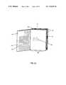
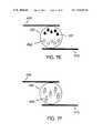
- FIGS. 1A and Bare partially perspective and partially schematic views of an electronic book with multiple electronically addressable pages.
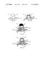
- FIG. 2Ais a partially perspective and partially schematic view of an electronic book with multiple electronically addressable pages open to a single such page.
- FIG. 2Bis a partially perspective and partially schematic view of an electronic book configured with column and row address electrodes on a preceding page and a ground plane on a following page.
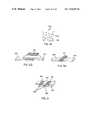
- FIG. 4is a schematic view of an electronically addressable page configured for multilayer address line layout and full page addressability with column strobe.
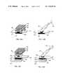
- FIG. 5Ais a schematic view of an electronically addressable page configured for row addressing with analog selected column lines.
- FIG. 5Bis a schematic detail of the analog column select scheme.
- FIG. 6Ais a schematic view of an electronically addressable page configured for row addressing with digital selected column lines.
- FIG. 6Bis a schematic detail of the digital column select scheme.
- FIG. 6Cis a schematic view of an electronically addressable page configured for digitally selected row lines and column lines.
- FIG. 6Dis a schematic detail of an array of row and column addressing lines suitable for in-plane switched or dielectrophoretic switched electronically addressable contrast media.
- FIGS. 7A-7Dare schematic details of various electronically addressable contrast media.
- FIGS. 7E-7Fare schematic details of a two part dye based electronically addressable contrast media.
- FIGS. 7G-7Lare schematic details of in plane switched and near in-plane switched electronically addressable contrast media.
- FIGS. 7M-Pare schematic details of dielectrophoretic switched electronically addressable contrast media.
- FIGS. 8A-8Eare schematic details of various switch and relay assemblies.
- FIGS. 9A-9Eare schematic details of various switch structures.
- FIGS. 9F-9Iare schematic details of various printed switch structures.
- FIGS. 11A and Bare partially perspective and partially schematic views of a single page of an electronic book and a means for binding a multiplicity of such pages.
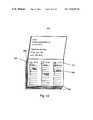
- FIG. 12is a schematic view of an electronic address/date book with multiple display pages.
- a book 10is composed of multiple electronically addressable page displays forming a multiple page display ensemble 20 in which each page of said ensemble may be individually electronically addressed.
- Said bookmay additionally contain: An internal power source 40 such as a battery; Electronic display drivers 50 to write information to said page displays where said drivers may write information contained in a memory or alternatively may write information obtained via a suitable interface or alternatively may write information from another source such as an electronic pen or stylus or from another suitable source.;
- Memory 60which may be a solid state memory such as flash memory or bubble memory or may be another form of memory such an optical disk or magnetic media or may be any other form of memory.
- Such memorymay contain information including text and/or graphics. Such information may be for instance the text and graphics of a selection of books or journals.
- said memorymay be programmable or reprogrammable. Alternatively said memory may be permanent. Said memory may also be removable for the purposes of reprogramming or for other purposes. Alternatively said memory may be a fixed memory. Said memory may also be interfaced to said electronic drivers and may further be interfaced to an external source.;
- a fast display 70which may be an LCD display for displaying a certain subset of the information contained in said memory such as book titles.
- Control buttons 80which may be used for accessing the information contained in said memory and causing said information to be displayed on said fast display or on said page displays or to access some other control function.
- a title space 30which may be composed of a similar electronically addressable structure to said page displays.;
- Additional electronic elements 90which may include a receiver or transmitter or other means of communications such as a data port or a modem or any other suitable interface. Said additional components may additionally contain a processor or microprocessor and any other components known in the art of computers or portable computers or any other electronic components useful in the operation of said electronic book.
- said book 10contains electronically addressable page displays 100 which combine to form an ensemble of multiple page displays 20 .
- Said bookmay additionally comprise a cover 140 and spine 130 which may hold various elements as described in reference to FIG. 1 .
- Such page displays 100are composed of a substrate 105 , an electronically addressable contrast media 120 , and address lines 110 .
- Said book 10 and said page displays 100are configured such that substantially different information can be written or electronically ‘typeset’ on the different page displays 100 which comprise the multiple page ensemble 20 .
- said page displaysmay be thin, low cost and formed on paper or paper like substrates.
- Such substratesmay be real paper, synthetic paper, ultra thin glass, plastic, polymer, elastomer, thin metal, carbon fiber or other suitable material which embody some or a majority of paper like qualities including thinness, structure, manipulability or other characteristics normally associated with paper in its role as a hapticly and visually interactable display of information.
- Said address linesmay be composed of transparent conducting polymers, transparent conductors such as Indium Tin Oxide, thin metal conductors or other suitable conductors. Such address lines may be applied by vacuum deposition, sputtering, photolithography or may be printed via ink jet systems or laser printer systems or may be applied via other appropriate means. Further such address lines may additionally be insulated with an appropriate insulator such as a non conducting polymer or other suitable insulator. Alternatively insulating layers may be applied in such manner to effect electrical isolation between row and row conducting lines, between row and column address lines, between column and column address lines or for other purposes of electrical isolation.
- Said contrast mediamay be electrochromic material, rotatable microencapsulated microspheres, polymer dispersed liquid crystals (PDLCS), polymer stabilized liquid crystals, surface stabilized liquid crystal, smectic liquid crystal, ferroelectric material, electroluminescent material or any other of a very large number of contrast media known in the prior art.
- Certain such contrast media, such as microencapsulated mediamay be printed via an ink jet or ink jet like system or may be applied via other appropriate means.
- FIG. 2Bis an electronic book configured with row 230 and column 210 electrodes on the back of a preceding page 107 and a ground plane 108 embedded in a following page 100 .
- Such an arrangementallows for addressing of said electronic page displays when said electronic book is in addressing of said electronic page displays when said electronic book is in the closed state while allowing said page displays to be viewed without having to look through a top a electrode when said book is in the open condition.
- the operation of such addressingis effected by either cancelling or adding to the electric field produced by address lines of the complimentary orthogonality.
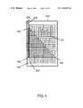
- FIG. 3depicts a preferred embodiment of a page display 100 incorporating a simplified address line scheme configured for partial page addressability.
- a substrate 105has deposited on or embedded in it an underlying array of row address lines 230 , an electronically addressable contrast media 120 and an array of column address lines 210 .
- a book configurationrequires that all address lines are substantially accessible along or near a single edge of the book page. Such is the case with the schemes described in this disclosure.
- row lines 230 and column lines 210are common to each page in the multiple page ensemble.
- Pagesare addressed individually via a page address strobe comprised of page address strobe control lines 200 and 205 and page address strobe switches 220 which control whether or not a particular page's column address lines are active in response to signal applied to said page address strobe control lines. It is understood however that in each of the embodiments described page strobing may be obviated in exchange for a more complicated spine driver in which each page in the multiple page ensemble may be wired directly and separately to the display driver.
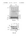
- FIG. 4depicts a preferred embodiment of a page display 100 incorporating a multilayer address line scheme configured for full page addressability.
- Edge column address line connectors 240are connected to column address lines 250 via a conducting connection 260 .
- Such a connectionmay be of conducting polymer, ITO, metal or other suitable conductor or may be a direct connection of the line 240 to 250 which may further be bonded with a laser weld or non conducting or conducting epoxy or other adhesive.
- In all other areas where column address line connectors 240 cross column address lines 250there is no conducting connection as effected by the placement of a suitable insulating layer.
- the page strobecomposed of page strobe control lines 200 and 205 and page strobe switches 220 operate as in FIG. 3 to control the state of said column address lines. As before column and row address lines may be common to each page in the multiple page ensemble.
- FIGS. 5A-Bare schematic views of an electronically addressable page 100 in which row lines 260 emanate from the page edge and are connected to the display driver. Row lines may be common to each page. Column address lines are analog selected by means of applying appropriate voltages between analog column switch control line 290 and 300 and 310 and 320 .
- Each column address line 270may be denoted by a number j between l and N where N is the total number of column address lines per page.
- Each column address linein turn is controlled via a set of two column switches, 330 and 340 , each of which in turn may be given designations k and l for the top and bottom control switches ( 330 and 340 ) respectively where k and l both range from l to N.
- Said column switches 330 and 340have a uniform threshold in which the column address lines 270 which they control become active (closed circuit, denoted by a black filled box) if said column switch's control lines 290 and 300 and 310 and 320 respectively have a potential difference greater than a threshold voltage V th as measured at said switch control line input.
- Resistors 350connect said switches 330 or 340 such that for a given applied potential difference on said switch control lines each switch sees a different and monotonicly scaled potential difference at its control line input face.
- the criterion for column address line j to be active and thus be at the potential V C applied to common column address line bias 280is: V 1 /( j*R )> V th and V 2 /(( N ⁇ j )* R )> V th
- V 1 and V 2a single column address line may be selected.
- black filled control switchesdenote a closed switch condition
- white filled control switchesdenote an open switch condition.
- the analog column switch control line or linesare unique and not common to each page thereby allowing for page selectability.
- FIGS. 6A-Bare schematic views of an electronically addressable page 100 in which row lines 260 emanate from the page edge and are connected to the display driver. Row lines may be common to each page. Column address lines are digital selected by means of applying appropriate logical values for digital column switch control lines 380 , 382 and 384 with ground 390 .
- the digital column select schemeoperates as follows: Rows of digital column switches 370 , 372 and 374 control column address lines such that all such said column switches in a given column must be in a closed circuit state (black filled box) for said column address line to be active. In order to control N column address lines it is required to have S rows of column switches such that S is the least integer greater than Log[N]/Log[2]. In the example shown in the detail 3 rows of such column switches 370 , 372 and 374 control 8 column address lines 270 .
- the first such rowis wired such that a logical 1 applied to the said row's column switch control line, 380 , yields a state in which the first N/2 switches are in a closed circuit state and the second N/2 switches are in an open circuit state.
- the second row, 382is wired such that said switch states alternate with a period of N*2 ⁇ 2 .
- the m th rowalternates with a period of N*2 ⁇ m .
- an electronically addressable page 100may be constructed in which both column address lines and row address lines are digitally selected. Such a scheme minimizes the total number of address lines emanating from the page and may simplify connections to off board address logic.
- Such a schemeemploys digital column switches 371 , digital column switch control lines 381 with ground 390 and column address line common terminal 395 as in FIG. 6A-B as well as digital row switches 373 , digital row switch control lines 383 with ground 391 and row address line common terminal 396 .
- the total number of leads required to emanate from the display page for the purpose of addressingare Log[Nc]/Log[2]+Log[Nr]/Log [2]+4 in which Nc are the number of column address lines and Nr are the number of row address lines.
- the additional 4provides for switch grounds and common terminal lines. It is recognized that an even smaller number of emanating leads may be employed by further addressing said switch control lines with a further bank of control switches.
- row electrodes 260 and column electrodes 270may be configured to perform an in-plane switching function by means of insulating said lines from each other by the addition of an insulating pad 264 and by addition of an added address line section 262 .
- Two such in-plane switching arrays, one lying on top of the otherare suitable for performing a dielectrophoretic switching function.
- a dielectric sphere 440 with substantially different contrast hemispheresmay be microencapsulated in a microcapsule 420 and may be free to rotate in a fluid 430 .
- the orientation of such a spheremay be controlled via the applied potential difference between electrode or address line 400 and 410 . If one or both such electrodes are substantially transparent then an electronically addressable contrast may be effected.
- Such systemsare known to posses inherent bistability or memory during open circuit due to electrostatic stiction.
- polymer dispersed liquid crystals (PDLCs) 450may be microencapsulated or encapsulated in a microcapsule or capsule 420 .
- said PDLCsare not oriented and are thus highly scattering and thus opaque. Under the application of a bias said PDLCs become aligned and are thus substantially transmitting.
- an electronically addressable contrastmay be effected.
- such a contrast systemmay be a polymer stabilized system as is known in the prior art such that said system exhibits bistability.
- oriented LCD molecules 470which may be microencapsulated in microcapsule 420 may be caused to rotationally orient and thus change the polarization of incident light upon application of a bias between 400 and 410 .
- said arrangementmay again effect an electronically addressable contrast media.
- an electrochromic material 480 and an electrolyte 490which may be a solid electrolyte are sandwiched between electrodes 400 and 410 .
- Application of a potential difference between said electrodeseffects an electronically addressable change of contrast.
- Said electrochromic systemsare known in the prior art to be capable of memory, threshold, color capabilities and operability with a solid electrolyte system.
- a dye material 491which may have an associated positive charge or may be bound to a particle with a positive charge may be brought into proximity or separated from the pH altering or solvent substance 492 which may have a negative charge or be bound to a particle with a negative charge by means of an electric field applied to electrodes 400 and 410 .
- Such a chemical systemwhich may encapsulated in capsule 420 , may constitute a field effect electronically addressable contrast media in such case as the color of said dye material is altered by said pH altering or solvent substance.
- a top transparent electrode 400may degrade the optical characteristics of the display. This may be accomplished in a reflective display by employing in-plane switching. In plane switching techniques have been employed in transmissive LCD displays for another purpose, namely to increase viewing angle of such displays. In the patent application Ser. No. 60/022,222, several in plane switching techniques may be employed to obviate the need for a top electrode. In one such system a dye material with an associated positive charge 491 and a pH or solvent substance with an associated negative charge 492 may be separated by means of an in plane electric field effected by means of application of a potential to in plane electrodes 495 and 496 . Such a system is viewed from above and thus said electrodes may be opaque and do not effect the optical characteristics of said display.
- a bistable liquid crystal system of the type demonstrated by Minoltais modified to be effected by in plane electrodes such that a liquid crystal mixture transforms from a first transparent planar structure 497 to a second scattering focal conic structure 498 .
- a near in-plane switching arrangementmay be realized in which a two color microsphere 440 is encapsulated in an outer capsule 420 which sit in a hole created by a middle electrode 498 . Applying a bias between said middle electrode 498 and a bottom electrode 497 causes said sphere to rotate as a function of the polarity of said bias.
- a field effect electrochromic contrast mediamay be realized by means of a microcapsule 420 containing phosphor particles 500 and photoconductive semiconductor particles and dye indicator particles 501 in a suitable binder 499 . Applying an AC field to electrodes 495 and 496 causes AC electroluminescence which causes free charge to be generated in the semiconducting material further causing said dye indicator to change color state.
- FIGS. 7M-7Pan entirely different means may be employed to effect a rear address of said contrast media.
- the dielectrophoretic effectis employed in which a species of higher dielectric constant may be caused to move to a region of high electric field.
- a non-colored dye solvent complex, 503which is stable when no field is applied across electrode pair 502 may be cause to dissociate into colored dye 504 and solvent 505 components by means of an electric field 506 effected by a potential on electrode pair 502 .
- stacked electrode pairs 502 and 507may be employed to effect a high field region in a higher 506 , or lower, 508 plane thus causing a higher dielectric constant material such as one hemisphere of a bichromal microsphere, 440 or one species 483 of a mixture of colored species, 483 and 484 to migrate to a higher or lower plane, respectively, and give the effect of differing color states.
- materials 509which may be dielectric materials or may be conducting materials may be employed to shape said electric fields.
- address line control switchesmeans are described for implementing address line control switches.
- address input line 510is separated from address output line 520 by means of space 570 which may contain a polarizable fluid, conducting beads or filings or other such substance such that when a bias is applied between switch control lines 530 and 540 setting up an electrostatic field through insulators 550 and 560 and space 570 such that a substantial decrease in resistivity is effected between lines 510 and 520 .
- address input line 510is separated from address output line 520 by means of space 600 which may contain magnetically poled microspheres 610 which have a substantially conducting hemisphere and a substantially insulating hemisphere.
- Space 600which may contain magnetically poled microspheres 610 which have a substantially conducting hemisphere and a substantially insulating hemisphere.
- Application of a current to loop control line 580effects a magnetic field as depicted which causes said microspheres to line up with said substantially conducting hemisphere oriented such that they bridge said gap or space 600 thus effecting a substantially closed circuit between 510 and 520 .
- Insulator 590insulates said switch control lines from said address lines.
- address input line 510is separated from address output line 520 by means of space 630 which contains magnetically poled and electrically conducting spheres 640 .
- Application of a current to switch control line 620effects the generation of a magnetic field as depicted causing said spheres to line up forming a conducting bridge between 510 and 520 as is known in the literature and thus effecting a substantially closed circuit between 510 and 520 .
- address input line 510has integral to it a conducting cantilever 515 separated from address output lines 520 by means of a gap.
- Application of a potential difference between line 510 and switch control line 650causes an electrostatic attraction between said cantilever and said address output line thus effecting a substantially closed circuit between 510 and 520 .
- Insulator 660insulates said switch control line from said address output line.
- address input line 510has integral to it a conducting cantilever which further has integral to it a magnetic substance 690 .
- Said magnetically active conducting cantileveris separated from address output lines 520 by means of a gap.
- Application of a current to switch control loop 670effects the generation of a magnetic field which causes said conducting cantilever to bend and make contact with said address output line thus effecting a substantially closed circuit between 510 and 520 .
- Insulator 680insulates said switch control line from said address output line.
- address input line 510is electrically isolated from address output line 520 .
- Layers of scandium diphthalocyanine (ScPc 2 ) 740 , Nickel Pthalocyanine (NiPc) 730 , Silicon Dioxide (SiO 2 ) 720 and n doped silicon (n-Si)bridge said address lines.
- a field-effect transistorin this case employing a dipthalocyanine thin film may be realized as is known in the literature.
- Such a structuremay act as an address control line switch as said gate 700 may substantially control the flow of current from said address input line 510 to said address output line 520 .
- address input line 510is isolated from address output line 520 by means of a stack including semiconducting polymer layers 750 and a switch control line 760 consisting of a camphor sulfonic acid protonated polyaniline (PANI-CSA) grid electrode filled with a semiconducting polymer.
- PANI-CSAcamphor sulfonic acid protonated polyaniline
- Such a structuremay act as an address control line switch as such structure as just described forms a polymer grid triode (PGT) as is known in the literature such that said switch control line 760 may substantially control the flow of current from said address input line 510 to said address output line 520 .
- Switch control line 760may alternatively consist of a metal film in which case the described structure forms a current switch.
- a bipolar spin switchis formed by means of paramagnetic metal film 850 and ferromagnetic films 870 and 880 .
- a bias applied between nonmagnetic metal electrode 860 and ferromagnetic film 870serves to regulate the current between input electrode 510 and output electrode 520 thus forming a switch as is known in the existing literature.
- a hall effect switchmay be effected whereby a potential may be formed across a hall effect material 910 between input electrode 510 and output electrode 520 by means of applying simultaneously an incident current injected by means of electrode 890 and collected by means of electrode 900 and a magnetic field H, perpendicular to said current, created by means of application of current to loop control line 670 and insulated by insulator 680 .
- curved resistor 930which is electrically but not thermally insulated by means of insulator 940 may be caused to be heated by means of application of a current to said resistor causing the impedance in thermistive material 920 , which posses a negative temperature coefficient of resistance, to drop thus lowering the impedance between input electrode 510 and output electrode 520 .
- Some of the above described devicessuch as those formed of conducting polymers have considerable utility in the present application as they posses the property of structural flexibility, tunable electronic properties and simplified deposition procedures (such as spin casting) which may be suitable for certain substrates such as real paper or paper like substrates. It is understood however that standard inorganic semiconductor technology such a Si or GaAs may be employed especially if suitable substrates such as ultra thin glass were employed for part or all of the page display.
- a semiconductor ink 943may be fabricated by dispersing a semiconductor powder 945 in a suitable binder 946 .
- Said semiconductive powdermay be Si, Germanium of GaAs or other suitable semiconductor and may further be doped, prior to being made into a powder, with n-type impurities such as phosphorous, antimony or arsenic or p-type impurities such as boron, gallium, indium or aluminum or other suitable n or p type dopants as is known in the art of semiconductor fabrication.
- Said binder 946may be a vinyl, plastic heat curable or UV curable material or other suitable binder as is known in the art of conducting inks. Such an binder 946 when cured brings into proximity said semiconductive powder particles 945 to create a continuous percolated structure with semiconductive properties.
- Said semiconductive ink 943may be applied by printing techniques to form switch or logic structures. As indicated in FIGS. 9F-I an NPN junction transistor may be fabricated consisting of a n-type emitter 950 , a p-type base 954 and a n-type collector 952 .
- a field effect transistormay be printed such as a metal oxide semiconductor.
- a transistorconsists of a p-type material metal oxide semiconductor.
- Such a transistorconsists of a p-type material 970 , an n-type material 966 an n-type inversion layer 968 an oxide layer 962 which acts as the gate a source lead 960 and a drain lead 964 .
- electroluminescent material 780is sandwiched between exciting electrodes 770 and 790 forming an electroluminescent light emitting structure which is electrically isolated by means of transparent isolator 795 .
- Emitted light from said electroluminescent light emitting structurecauses photoconductor 760 to undergo a decrease in impedance thus lowering the effective impedance between input electrode 510 and output electrode 520 as is known in the literature.
- Layer 800is an opaque layer which serves to optically shield other components from said light emitting structure.
- a switchmay be constructed where said electroluminescent light emitting structure is replaced by an optical fiber 802 which may be modified to scatter light to said photoconductor 760 and optical fiber light source 804 which may be a light emitting diode or laser diode or other suitable light source.
- said photoconductormay be replaced by a photodiode composed of an output electrode 510 with aperture 805 , a heavily doped p+ layer 810 , a depletion layer 820 , a lightly doped n-type layer 830 , an n+ layer 840 and an input electrode 520 .
- a photodiodecomposed of an output electrode 510 with aperture 805 , a heavily doped p+ layer 810 , a depletion layer 820 , a lightly doped n-type layer 830 , an n+ layer 840 and an input electrode 520 .
- any other photodiode or phototransistor structureas is known in the prior art may be employed.
- FIGS. 11A and Bdepict a preferred construction of a single electronically addressable page 100 and the means by which a multiplicity of said pages may be bound to form an ensemble of multiple page displays 20 .
- primary page substrate 105may additionally encompass a second substrate part 150 which may be of a different material than said primary substrate such as a plastic or glass material with substantially different mechanical or electronic properties than the primary substrate material.
- Said second substrate materialmay have situated upon it page strobe or address logic 165 and page strobe or page address control lines 175 .
- Said second substratemay further encompass apertures 160 .
- Such single page displays 100may be combined to form a page display ensemble 20 .
- Row or column address lines 110may be connected to said apertures 160 such that display driver lines 185 may connect said address lines of each page 100 in said page ensemble thus forming common address lines from page to page.
- Such display driver linesmay then further be connected to display driver 180 .
- Such display driver lines which are common to each display page and which further connect through said apertures of said display pagesmay further serve to mechanically bind said pages to form said page display ensemble.
- Page strobe or page address lines 175which are not common to each page may be connected to page strobe or page address driver 170 .
- said substrate 105may be of a single material.
- said apertures 160may be obviated and said control lines may be extended to the page edge where they may be connected to said driver lines.
- additional mechanical bindingsmay be employed to mechanically bind said pages. It is readily understood that additional or alternative techniques of mechanical binding as is known in the art of book manufacture and other means of electrical connection as is known in the art of electronics and display manufacture may be employed.
- an electronic address book/date book 980 with multiple electronically addressable display pages, 988said book may have driver electronics, 986 and an interface 984 to another computer of computer network.
- Said interface 984may be wired or wireless or optical.
- said address book/date bookmay be permanently W printed information 983 as well as changeable information 982 .
Landscapes
- Physics & Mathematics (AREA)
- Engineering & Computer Science (AREA)
- Nonlinear Science (AREA)
- Chemical & Material Sciences (AREA)
- General Physics & Mathematics (AREA)
- Optics & Photonics (AREA)
- Crystallography & Structural Chemistry (AREA)
- Theoretical Computer Science (AREA)
- Mathematical Physics (AREA)
- Life Sciences & Earth Sciences (AREA)
- Nanotechnology (AREA)
- Materials Engineering (AREA)
- Computer Hardware Design (AREA)
- Organic Chemistry (AREA)
- Wood Science & Technology (AREA)
- Health & Medical Sciences (AREA)
- Molecular Biology (AREA)
- Geometry (AREA)
- Biophysics (AREA)
- Computing Systems (AREA)
- Dispersion Chemistry (AREA)
- General Engineering & Computer Science (AREA)
- Microelectronics & Electronic Packaging (AREA)
- Chemical Kinetics & Catalysis (AREA)
- Electrochemistry (AREA)
- Electrochromic Elements, Electrophoresis, Or Variable Reflection Or Absorption Elements (AREA)
Abstract
Description
This application is a 371 of PCT/US96/12000 filed on Jul. 19, 1996 which is, as regards the United States, a continuation-in-part of 08/504,896, filed Jul. 20, 1995, now U.S. Pat No. 6,124,851.
Presently the concept of an electronic book (such as the omni book concept invented by Alan Kay now of Apple Computer) connotes a device with a single electronically addressable display in which pages of text are displayed sequentially in time as a function of some input. Further, in EPO 618 715 A, an electronic notebook having three pages of addressable liquid crystal displays is disclosed. On the other hand real paper books contain multiple pages which may be accessed by means of a natural haptic input. Such pages however, once printed, are not changeable.
In this disclosure we describe an electronic book with multiple electronically addressable displays. Such an electronic book embodies the representation of information on a multiplicity of physical pages which may be may be electronically addressed or ‘typeset’ such that the contents of said pages may be changed by means of an electronic signal and which may further be handled, physically moved and written on. The advantages of the present invention include the ability, from within a single electronic book, to access a large realm of information, which would normally encompass many volumes of standard paper books while still maintaining the highly preferred natural haptic and visual interface of said normal paper books. As such, an electronic book with multiple electronically addressable page displays, as disclosed, herein, constitutes a highly useful means of information interaction.
The invention provides for an electronic book with multiple electronically addressable page displays. In one embodiment such page displays may be thin, low cost and formed on paper or paper like substrates. Such substrates may be real paper, ultra thin glass, plastic, polymer, elastomer or other suitable material which embody some or a majority of paper like qualities including thinness, structure, manipulability or other characteristics normally associated with paper in its role as a hapticly and visually interactable display of information. Said page displays additionally comprise address lines and electronically addressable contrast media which may be bistable media such that texts or images written to said page displays may be maintained without the application of power. Said page displays may further comprise page strobe or page address logic for the purpose of electrically addressing a particular page in said multiple page display book.
Said book may additionally contain electronic memory, an internal power source, controls and interfaces, which may either be wired, wireless or optical, for interfacing to various sources of data or communications. Such an electronic memory may contain the informational content, both textual and graphical, comprised in a multiplicity of normal paper books. A user may then select a book of choice and cause, by means of a control, the electronically addressable pages of said book to be ‘typeset’ such that after some time delay the pages of said electronic book display the desired contents.
The invention provides for means of manufacturing the pages of said electronic book in a low cost way on a paper or paper like substrate. The invention further provides for means of binding such pages and addressing such a multiple page electronic book. Additional features including an interface and the ability to write in a reversible manner and have such writing recorded are also described. Further features and aspects will become apparent from the following description and from the claims.
The foregoing and other objects, features and advantages of the invention will be apparent from the following more particular description of preferred embodiments of the invention, as illustrated in the accompanying drawings in which like reference characters refer to the same parts throughout the different views. The drawings are not necessarily to scale, emphasis instead being placed upon illustrating the principles of the invention.
Referring toFIG. 1 , abook 10 is composed of multiple electronically addressable page displays forming a multiplepage display ensemble 20 in which each page of said ensemble may be individually electronically addressed. Said book may additionally contain: Aninternal power source 40 such as a battery;Electronic display drivers 50 to write information to said page displays where said drivers may write information contained in a memory or alternatively may write information obtained via a suitable interface or alternatively may write information from another source such as an electronic pen or stylus or from another suitable source.;Memory 60 which may be a solid state memory such as flash memory or bubble memory or may be another form of memory such an optical disk or magnetic media or may be any other form of memory. Such memory may contain information including text and/or graphics. Such information may be for instance the text and graphics of a selection of books or journals. Further said memory may be programmable or reprogrammable. Alternatively said memory may be permanent. Said memory may also be removable for the purposes of reprogramming or for other purposes. Alternatively said memory may be a fixed memory. Said memory may also be interfaced to said electronic drivers and may further be interfaced to an external source.; Afast display 70 which may be an LCD display for displaying a certain subset of the information contained in said memory such as book titles.;Control buttons 80 which may be used for accessing the information contained in said memory and causing said information to be displayed on said fast display or on said page displays or to access some other control function.; Atitle space 30 which may be composed of a similar electronically addressable structure to said page displays.; Additionalelectronic elements 90 which may include a receiver or transmitter or other means of communications such as a data port or a modem or any other suitable interface. Said additional components may additionally contain a processor or microprocessor and any other components known in the art of computers or portable computers or any other electronic components useful in the operation of said electronic book.
Referring toFIG. 2A saidbook 10 contains electronically addressable page displays100 which combine to form an ensemble of multiple page displays20. Said book may additionally comprise acover 140 andspine 130 which may hold various elements as described in reference to FIG.1. Such page displays100 are composed of asubstrate 105, an electronicallyaddressable contrast media 120, and address lines110. Saidbook 10 and said page displays100 are configured such that substantially different information can be written or electronically ‘typeset’ on thedifferent page displays 100 which comprise themultiple page ensemble 20.
In a preferred embodiment said page displays may be thin, low cost and formed on paper or paper like substrates. Such substrates may be real paper, synthetic paper, ultra thin glass, plastic, polymer, elastomer, thin metal, carbon fiber or other suitable material which embody some or a majority of paper like qualities including thinness, structure, manipulability or other characteristics normally associated with paper in its role as a hapticly and visually interactable display of information.
Said address lines may be composed of transparent conducting polymers, transparent conductors such as Indium Tin Oxide, thin metal conductors or other suitable conductors. Such address lines may be applied by vacuum deposition, sputtering, photolithography or may be printed via ink jet systems or laser printer systems or may be applied via other appropriate means. Further such address lines may additionally be insulated with an appropriate insulator such as a non conducting polymer or other suitable insulator. Alternatively insulating layers may be applied in such manner to effect electrical isolation between row and row conducting lines, between row and column address lines, between column and column address lines or for other purposes of electrical isolation.
Said contrast media may be electrochromic material, rotatable microencapsulated microspheres, polymer dispersed liquid crystals (PDLCS), polymer stabilized liquid crystals, surface stabilized liquid crystal, smectic liquid crystal, ferroelectric material, electroluminescent material or any other of a very large number of contrast media known in the prior art. Certain such contrast media, such as microencapsulated media may be printed via an ink jet or ink jet like system or may be applied via other appropriate means.
Referring to the detail, the analog column select scheme operates as follows: Eachcolumn address line 270 may be denoted by a number j between l and N where N is the total number of column address lines per page. Each column address line in turn is controlled via a set of two column switches,330 and340, each of which in turn may be given designations k and l for the top and bottom control switches (330 and340) respectively where k and l both range from l to N.
Said column switches330 and340 have a uniform threshold in which thecolumn address lines 270 which they control become active (closed circuit, denoted by a black filled box) if said column switch'scontrol lines Resistors 350 connect saidswitches control line control lines address line bias 280 is:
V1/(j*R)>VthandV2/((N−j)*R)>Vth
Thus by choosing an appropriate value of V1and V2a single column address line may be selected. In the example shown in the detail black filled control switches denote a closed switch condition and white filled control switches denote an open switch condition.Column line 2 has been made active by the appropriate choice of V1and V2whereas all other column lines are inactive as for all other column lines at least one column control switch is in the open circuit state. It is understood that a further simplification may be made by making V2=constant −V1such that only a single voltage line need be addressed. The analog column switch control line or lines are unique and not common to each page thereby allowing for page selectability.
V1/(j*R)>VthandV2/((N−j)*R)>Vth
Thus by choosing an appropriate value of V1and V2a single column address line may be selected. In the example shown in the detail black filled control switches denote a closed switch condition and white filled control switches denote an open switch condition.
Referring to the detail, the digital column select scheme operates as follows: Rows of digital column switches370,372 and374 control column address lines such that all such said column switches in a given column must be in a closed circuit state (black filled box) for said column address line to be active. In order to control N column address lines it is required to have S rows of column switches such that S is the least integer greater than Log[N]/Log[2]. In the example shown in thedetail 3 rows of such column switches370,372 and374control 8 column address lines270. The first such row is wired such that a logical1 applied to the said row's column switch control line,380, yields a state in which the first N/2 switches are in a closed circuit state and the second N/2 switches are in an open circuit state. The second row,382, is wired such that said switch states alternate with a period of N*2−2. The mthrow alternates with a period of N*2−m. Such a configuration allows for the unique selection of a single column address line such that said selected column address line becomes active with the potential applied to commoncolumn address bias 395. In the example shown in the detailcolumn address line 3 becomes active upon application of thelogical values switch control lines
Referring toFIG. 6C an electronicallyaddressable page 100 may be constructed in which both column address lines and row address lines are digitally selected. Such a scheme minimizes the total number of address lines emanating from the page and may simplify connections to off board address logic. Such a scheme employs digital column switches371, digital columnswitch control lines 381 withground 390 and column address linecommon terminal 395 as inFIG. 6A-B as well as digital row switches373, digital rowswitch control lines 383 withground 391 and row address linecommon terminal 396. In this implementation the total number of leads required to emanate from the display page for the purpose of addressing are Log[Nc]/Log[2]+Log[Nr]/Log [2]+4 in which Nc are the number of column address lines and Nr are the number of row address lines. The additional 4 provides for switch grounds and common terminal lines. It is recognized that an even smaller number of emanating leads may be employed by further addressing said switch control lines with a further bank of control switches.
Finally it is also understood that any other suitable digital scheme in which each page has a page address may be employed as is known in the literature and prior art of display addressing.
Referring toFIG.6D row electrodes 260 andcolumn electrodes 270 may be configured to perform an in-plane switching function by means of insulating said lines from each other by the addition of an insulatingpad 264 and by addition of an addedaddress line section 262. Two such in-plane switching arrays, one lying on top of the other are suitable for performing a dielectrophoretic switching function.
Referring toFIGS. 7A-D a great many electronically addressable contrast media are known in the literature and prior art. In one embodiment adielectric sphere 440 with substantially different contrast hemispheres may be microencapsulated in amicrocapsule 420 and may be free to rotate in afluid 430. The orientation of such a sphere may be controlled via the applied potential difference between electrode oraddress line
In another system polymer dispersed liquid crystals (PDLCs)450 may be microencapsulated or encapsulated in a microcapsule orcapsule 420. In the absence of an applied bias betweenelectrodes
In another system orientedLCD molecules 470 which may be microencapsulated inmicrocapsule 420 may be caused to rotationally orient and thus change the polarization of incident light upon application of a bias between400 and410. When viewed through apolarizer 460 said arrangement may again effect an electronically addressable contrast media.
In another system anelectrochromic material 480 and anelectrolyte 490 which may be a solid electrolyte are sandwiched betweenelectrodes
Referring toFIGS. 7E-F , another system, described in the patent application Ser. No. 60/022,222 by Joseph M. Jacobson filed on Jul. 19, 1996, adye material 491 which may have an associated positive charge or may be bound to a particle with a positive charge may be brought into proximity or separated from the pH altering orsolvent substance 492 which may have a negative charge or be bound to a particle with a negative charge by means of an electric field applied toelectrodes capsule 420, may constitute a field effect electronically addressable contrast media in such case as the color of said dye material is altered by said pH altering or solvent substance.
Referring toFIGS. 7G-L , it may be desirable to avoid the use of a toptransparent electrode 400 as such electrodes may degrade the optical characteristics of the display. This may be accomplished in a reflective display by employing in-plane switching. In plane switching techniques have been employed in transmissive LCD displays for another purpose, namely to increase viewing angle of such displays. In the patent application Ser. No. 60/022,222, several in plane switching techniques may be employed to obviate the need for a top electrode. In one such system a dye material with an associatedpositive charge 491 and a pH or solvent substance with an associatednegative charge 492 may be separated by means of an in plane electric field effected by means of application of a potential to inplane electrodes
In another such system a bistable liquid crystal system of the type demonstrated by Minolta is modified to be effected by in plane electrodes such that a liquid crystal mixture transforms from a first transparentplanar structure 497 to a second scattering focalconic structure 498.
In another scheme, suitable for two color microspheres, a near in-plane switching arrangement may be realized in which a twocolor microsphere 440 is encapsulated in anouter capsule 420 which sit in a hole created by amiddle electrode 498. Applying a bias between saidmiddle electrode 498 and abottom electrode 497 causes said sphere to rotate as a function of the polarity of said bias.
In another scheme a field effect electrochromic contrast media may be realized by means of amicrocapsule 420 containingphosphor particles 500 and photoconductive semiconductor particles anddye indicator particles 501 in asuitable binder 499. Applying an AC field toelectrodes
Referring toFIGS. 7M-7P an entirely different means may be employed to effect a rear address of said contrast media. In these schemes, disclosed in the patent application Ser. No. 60/022,222, the dielectrophoretic effect is employed in which a species of higher dielectric constant may be caused to move to a region of high electric field.
Referring toFIGS. 7M and 7N a non-colored dye solvent complex,503, which is stable when no field is applied acrosselectrode pair 502 may be cause to dissociate intocolored dye 504 and solvent505 components by means of anelectric field 506 effected by a potential onelectrode pair 502.
In another system stacked electrode pairs502 and507 may be employed to effect a high field region in a higher506, or lower,508 plane thus causing a higher dielectric constant material such as one hemisphere of a bichromal microsphere,440 or onespecies 483 of a mixture of colored species,483 and484 to migrate to a higher or lower plane, respectively, and give the effect of differing color states. Insuch schemes materials 509 which may be dielectric materials or may be conducting materials may be employed to shape said electric fields.
It is understood that any other electronically addressable contrast media may readily be substituted for those described above.
Referring toFIGS. 8A-E means are described for implementing address line control switches. Referring to the left uppermost figureaddress input line 510 is separated fromaddress output line 520 by means ofspace 570 which may contain a polarizable fluid, conducting beads or filings or other such substance such that when a bias is applied betweenswitch control lines insulators space 570 such that a substantial decrease in resistivity is effected betweenlines
In another systemaddress input line 510 is separated fromaddress output line 520 by means ofspace 600 which may contain magnetically poledmicrospheres 610 which have a substantially conducting hemisphere and a substantially insulating hemisphere. Application of a current toloop control line 580 effects a magnetic field as depicted which causes said microspheres to line up with said substantially conducting hemisphere oriented such that they bridge said gap orspace 600 thus effecting a substantially closed circuit between510 and520.Insulator 590 insulates said switch control lines from said address lines.
In another systemaddress input line 510 is separated fromaddress output line 520 by means ofspace 630 which contains magnetically poled and electrically conductingspheres 640. Application of a current to switchcontrol line 620 effects the generation of a magnetic field as depicted causing said spheres to line up forming a conducting bridge between510 and520 as is known in the literature and thus effecting a substantially closed circuit between510 and520.
In another systemaddress input line 510 has integral to it a conductingcantilever 515 separated fromaddress output lines 520 by means of a gap. Application of a potential difference betweenline 510 and switchcontrol line 650 causes an electrostatic attraction between said cantilever and said address output line thus effecting a substantially closed circuit between510 and520.Insulator 660 insulates said switch control line from said address output line.
In another systemaddress input line 510 has integral to it a conducting cantilever which further has integral to it amagnetic substance 690. Said magnetically active conducting cantilever is separated fromaddress output lines 520 by means of a gap. Application of a current to switchcontrol loop 670 effects the generation of a magnetic field which causes said conducting cantilever to bend and make contact with said address output line thus effecting a substantially closed circuit between510 and520.Insulator 680 insulates said switch control line from said address output line.
Referring toFIGS. 9A-E several schemes are known in the literature and the prior art for effecting an electronic switch or transistor function without moving parts. Referring to the upper figureaddress input line 510 is electrically isolated fromaddress output line 520. Layers of scandium diphthalocyanine (ScPc2)740, Nickel Pthalocyanine (NiPc)730, Silicon Dioxide (SiO2)720 and n doped silicon (n-Si) bridge said address lines. By incorporating a control gate700 a field-effect transistor in this case employing a dipthalocyanine thin film may be realized as is known in the literature. Such a structure may act as an address control line switch as saidgate 700 may substantially control the flow of current from saidaddress input line 510 to saidaddress output line 520.
In another arrangementaddress input line 510 is isolated fromaddress output line 520 by means of a stack including semiconducting polymer layers750 and aswitch control line 760 consisting of a camphor sulfonic acid protonated polyaniline (PANI-CSA) grid electrode filled with a semiconducting polymer. Such a structure may act as an address control line switch as such structure as just described forms a polymer grid triode (PGT) as is known in the literature such that saidswitch control line 760 may substantially control the flow of current from saidaddress input line 510 to saidaddress output line 520.Switch control line 760 may alternatively consist of a metal film in which case the described structure forms a current switch.
In another scheme a bipolar spin switch is formed by means ofparamagnetic metal film 850 andferromagnetic films nonmagnetic metal electrode 860 andferromagnetic film 870 serves to regulate the current betweeninput electrode 510 andoutput electrode 520 thus forming a switch as is known in the existing literature.
In another scheme a hall effect switch may be effected whereby a potential may be formed across ahall effect material 910 betweeninput electrode 510 andoutput electrode 520 by means of applying simultaneously an incident current injected by means ofelectrode 890 and collected by means ofelectrode 900 and a magnetic field H, perpendicular to said current, created by means of application of current toloop control line 670 and insulated byinsulator 680.
In another scheme,curved resistor 930 which is electrically but not thermally insulated by means ofinsulator 940 may be caused to be heated by means of application of a current to said resistor causing the impedance inthermistive material 920, which posses a negative temperature coefficient of resistance, to drop thus lowering the impedance betweeninput electrode 510 andoutput electrode 520.
Some of the above described devices such as those formed of conducting polymers have considerable utility in the present application as they posses the property of structural flexibility, tunable electronic properties and simplified deposition procedures (such as spin casting) which may be suitable for certain substrates such as real paper or paper like substrates. It is understood however that standard inorganic semiconductor technology such a Si or GaAs may be employed especially if suitable substrates such as ultra thin glass were employed for part or all of the page display.
Referring toFIGS. 9F-I in addition to standard semiconductor technology which involves deposition and subsequent etching it may be useful, especially on atypical substrates, to deposit a semiconductor ink from which transistors and switches may be fabricated. As described in the patent application Ser. No. 60/022,222, asemiconductor ink 943 may be fabricated by dispersing asemiconductor powder 945 in asuitable binder 946. Said semiconductive powder may be Si, Germanium of GaAs or other suitable semiconductor and may further be doped, prior to being made into a powder, with n-type impurities such as phosphorous, antimony or arsenic or p-type impurities such as boron, gallium, indium or aluminum or other suitable n or p type dopants as is known in the art of semiconductor fabrication.Said binder 946 may be a vinyl, plastic heat curable or UV curable material or other suitable binder as is known in the art of conducting inks. Such anbinder 946 when cured brings into proximity saidsemiconductive powder particles 945 to create a continuous percolated structure with semiconductive properties. Saidsemiconductive ink 943 may be applied by printing techniques to form switch or logic structures. As indicated inFIGS. 9F-I an NPN junction transistor may be fabricated consisting of a n-type emitter 950, a p-type base 954 and a n-type collector 952.
Alternatively a field effect transistor may be printed such as a metal oxide semiconductor. Such a transistor consists of a p-type material metal oxide semiconductor. Such a transistor consists of a p-type material 970, an n-type material 966 an n-type inversion layer 968 anoxide layer 962 which acts as the gate asource lead 960 and adrain lead 964.
Referring toFIGS. 10A-D means are described for implementing control switches based on optical control or optoelectronic devices. Referring to the left uppermostfigure electroluminescent material 780 is sandwiched betweenexciting electrodes transparent isolator 795. Emitted light from said electroluminescent light emitting structure causesphotoconductor 760 to undergo a decrease in impedance thus lowering the effective impedance betweeninput electrode 510 andoutput electrode 520 as is known in the literature.Layer 800 is an opaque layer which serves to optically shield other components from said light emitting structure.
Alternatively a switch may be constructed where said electroluminescent light emitting structure is replaced by anoptical fiber 802 which may be modified to scatter light to saidphotoconductor 760 and opticalfiber light source 804 which may be a light emitting diode or laser diode or other suitable light source.
In another arrangement, said photoconductor may be replaced by a photodiode composed of anoutput electrode 510 withaperture 805, a heavily dopedp+ layer 810, adepletion layer 820, a lightly doped n-type layer 830, ann+ layer 840 and aninput electrode 520. Alternatively it is understood that any other photodiode or phototransistor structure as is known in the prior art may be employed.
Referring to the perspective view of a multiplicity of pages such single page displays100 may be combined to form apage display ensemble 20. Row orcolumn address lines 110 may be connected to saidapertures 160 such thatdisplay driver lines 185 may connect said address lines of eachpage 100 in said page ensemble thus forming common address lines from page to page. Such display driver lines may then further be connected to displaydriver 180. Such display driver lines which are common to each display page and which further connect through said apertures of said display pages may further serve to mechanically bind said pages to form said page display ensemble. Page strobe orpage address lines 175 which are not common to each page may be connected to page strobe orpage address driver 170.
Alternatively saidsubstrate 105 may be of a single material. In another configuration saidapertures 160 may be obviated and said control lines may be extended to the page edge where they may be connected to said driver lines. In another configuration additional mechanical bindings may be employed to mechanically bind said pages. It is readily understood that additional or alternative techniques of mechanical binding as is known in the art of book manufacture and other means of electrical connection as is known in the art of electronics and display manufacture may be employed.
Referring toFIG. 12 the materials and configurations of the previous descriptives may be employed to construct an electronic address book/date book 980 with multiple electronically addressable display pages,988, said book may have driver electronics,986 and aninterface 984 to another computer of computer network. Saidinterface 984 may be wired or wireless or optical. Finally said address book/date book may be permanently W printedinformation 983 as well aschangeable information 982.
While this invention has been particularly shown and described with references to preferred embodiments thereof, it will be understood by those skilled in the art that various changes in form and details may be made therein without departing from the spirit and scope of the invention as defined by the appended claims.
Claims (5)
1. An electronically addressable display comprising:
a microencapsulated display media including a first species having a higher dielectric constant and a second species having a lower dielectric constant; and
at least two pairs of electrodes disposed adjacent the display media for selectively creating a region of higher electric field in a higher plane or a lower plane of the display media by one pair of the electrodes and a region of lower electric field by the other pair of electrodes, wherein the pair of electrodes responsible for the region of higher electric field are disposed adjacent one surface of the display media; and wherein the first species moves toward the region of higher electric field.
2. The electronically addressable display ofclaim 1 , wherein the display media comprises a bichromal microsphere having a first hemisphere and a second hemisphere differing in dielectric constants, wherein the first species of higher dielectric constant comprises the first hemisphere and the second species of lower dielectric constant comprises the second hemisphere.
3. The electronically addressable display ofclaim 1 wherein the display media comprises a first species of colored particles having a higher dielectric constant and a second species of colored particles having a lower dielectric constant.
4. The electronically addressable display ofclaim 1 wherein the first species has a dielectric constant that is permanently higher than that of the second species.
5. The electronically addressable display ofclaim 1 wherein the first species moves in translational migration.
Priority Applications (22)
| Application Number | Priority Date | Filing Date | Title |
|---|---|---|---|
| US08/983,404US7106296B1 (en) | 1995-07-20 | 1996-07-19 | Electronic book with multiple page displays |
| US09/513,411US6249271B1 (en) | 1995-07-20 | 2000-02-25 | Retroreflective electrophoretic displays and materials for making the same |
| US09/896,546US7071913B2 (en) | 1995-07-20 | 2001-06-29 | Retroreflective electrophoretic displays and materials for making the same |
| US10/329,023US7109968B2 (en) | 1995-07-20 | 2002-12-24 | Non-spherical cavity electrophoretic displays and methods and materials for making the same |
| US10/687,166US7259744B2 (en) | 1995-07-20 | 2003-10-16 | Dielectrophoretic displays |
| US10/701,880US7304634B2 (en) | 1995-07-20 | 2003-11-05 | Rear electrode structures for electrophoretic displays |
| US10/729,044US7352353B2 (en) | 1995-07-20 | 2003-12-05 | Electrostatically addressable electrophoretic display |
| US10/906,019US8139050B2 (en) | 1995-07-20 | 2005-01-31 | Addressing schemes for electronic displays |
| US11/162,188US7999787B2 (en) | 1995-07-20 | 2005-08-31 | Methods for driving electrophoretic displays using dielectrophoretic forces |
| US11/426,672US7391555B2 (en) | 1995-07-20 | 2006-06-27 | Non-spherical cavity electrophoretic displays and materials for making the same |
| US11/799,377US7583251B2 (en) | 1995-07-20 | 2007-05-01 | Dielectrophoretic displays |
| US11/962,543US7956841B2 (en) | 1995-07-20 | 2007-12-21 | Stylus-based addressing structures for displays |
| US11/962,680US8089453B2 (en) | 1995-07-20 | 2007-12-21 | Stylus-based addressing structures for displays |
| US11/970,811US8384658B2 (en) | 1995-07-20 | 2008-01-08 | Electrostatically addressable electrophoretic display |
| US12/059,306US7746544B2 (en) | 1995-07-20 | 2008-03-31 | Electro-osmotic displays and materials for making the same |
| US12/117,974US7791789B2 (en) | 1995-07-20 | 2008-05-09 | Multi-color electrophoretic displays and materials for making the same |
| US12/121,246US7848006B2 (en) | 1995-07-20 | 2008-05-15 | Electrophoretic displays with controlled amounts of pigment |
| US12/406,666US20090174651A1 (en) | 1995-07-20 | 2009-03-18 | Addressing schemes for electronic displays |
| US12/549,763US8305341B2 (en) | 1995-07-20 | 2009-08-28 | Dielectrophoretic displays |
| US12/754,227US8593718B2 (en) | 1995-07-20 | 2010-04-05 | Electro-osmotic displays and materials for making the same |
| US13/092,634US20110193840A1 (en) | 1995-07-20 | 2011-04-22 | Methods for driving electrophoretic displays using dielectrophoretic forces |
| US14/088,552US20140078573A1 (en) | 1995-07-20 | 2013-11-25 | Electro-osmotic displays and materials for making the same |
Applications Claiming Priority (3)
| Application Number | Priority Date | Filing Date | Title |
|---|---|---|---|
| US08/504,896US6124851A (en) | 1995-07-20 | 1995-07-20 | Electronic book with multiple page displays |
| PCT/US1996/012000WO1997004398A2 (en) | 1995-07-20 | 1996-07-19 | Electronic book with multiple page displays |
| US08/983,404US7106296B1 (en) | 1995-07-20 | 1996-07-19 | Electronic book with multiple page displays |
Related Parent Applications (6)
| Application Number | Title | Priority Date | Filing Date |
|---|---|---|---|
| US08/504,896Continuation-In-PartUS6124851A (en) | 1995-07-20 | 1995-07-20 | Electronic book with multiple page displays |
| US08/504,896ContinuationUS6124851A (en) | 1995-07-20 | 1995-07-20 | Electronic book with multiple page displays |
| PCT/US1996/012000A-371-Of-InternationalWO1997004398A2 (en) | 1995-07-20 | 1996-07-19 | Electronic book with multiple page displays |
| US08/935,800Continuation-In-PartUS6120588A (en) | 1995-07-20 | 1997-09-23 | Electronically addressable microencapsulated ink and display thereof |
| US09/140,988ContinuationUS6262706B1 (en) | 1995-07-20 | 1998-08-27 | Retroreflective electrophoretic displays and materials for making the same |
| US09/140,860Continuation-In-PartUS6710540B1 (en) | 1995-07-20 | 1998-08-27 | Electrostatically-addressable electrophoretic display |
Related Child Applications (11)
| Application Number | Title | Priority Date | Filing Date |
|---|---|---|---|
| US08/504,896Continuation-In-PartUS6124851A (en) | 1995-07-20 | 1995-07-20 | Electronic book with multiple page displays |
| US09/140,988Continuation-In-PartUS6262706B1 (en) | 1995-07-20 | 1998-08-27 | Retroreflective electrophoretic displays and materials for making the same |
| US09/140,846Continuation-In-PartUS6727881B1 (en) | 1995-07-20 | 1998-08-27 | Encapsulated electrophoretic displays and methods and materials for making the same |
| US09/141,041Continuation-In-PartUS6459418B1 (en) | 1995-07-20 | 1998-08-27 | Displays combining active and non-active inks |
| US09/140,860Continuation-In-PartUS6710540B1 (en) | 1995-07-20 | 1998-08-27 | Electrostatically-addressable electrophoretic display |
| US09/513,411ContinuationUS6249271B1 (en) | 1995-07-20 | 2000-02-25 | Retroreflective electrophoretic displays and materials for making the same |
| US10/329,023Continuation-In-PartUS7109968B2 (en) | 1995-07-20 | 2002-12-24 | Non-spherical cavity electrophoretic displays and methods and materials for making the same |
| US10/687,166Continuation-In-PartUS7259744B2 (en) | 1995-07-20 | 2003-10-16 | Dielectrophoretic displays |
| US10/729,044Continuation-In-PartUS7352353B2 (en) | 1995-07-20 | 2003-12-05 | Electrostatically addressable electrophoretic display |
| US10/906,019Continuation-In-PartUS8139050B2 (en) | 1995-07-20 | 2005-01-31 | Addressing schemes for electronic displays |
| US11/162,188Continuation-In-PartUS7999787B2 (en) | 1995-07-20 | 2005-08-31 | Methods for driving electrophoretic displays using dielectrophoretic forces |
Publications (1)
| Publication Number | Publication Date |
|---|---|
| US7106296B1true US7106296B1 (en) | 2006-09-12 |
Family
ID=36951821
Family Applications (2)
| Application Number | Title | Priority Date | Filing Date |
|---|---|---|---|
| US08/983,404Expired - Fee RelatedUS7106296B1 (en) | 1995-07-20 | 1996-07-19 | Electronic book with multiple page displays |
| US09/513,411Expired - Fee RelatedUS6249271B1 (en) | 1995-07-20 | 2000-02-25 | Retroreflective electrophoretic displays and materials for making the same |
Family Applications After (1)
| Application Number | Title | Priority Date | Filing Date |
|---|---|---|---|
| US09/513,411Expired - Fee RelatedUS6249271B1 (en) | 1995-07-20 | 2000-02-25 | Retroreflective electrophoretic displays and materials for making the same |
Country Status (1)
| Country | Link |
|---|---|
| US (2) | US7106296B1 (en) |
Cited By (122)
| Publication number | Priority date | Publication date | Assignee | Title |
|---|---|---|---|---|
| US20040252076A1 (en)* | 2003-03-31 | 2004-12-16 | Yoshiyuki Kodama | Display device, electronic device and display method |
| US20050185104A1 (en)* | 2002-07-25 | 2005-08-25 | Genewave | Optically active glazing |
| US7230751B2 (en) | 2005-01-26 | 2007-06-12 | E Ink Corporation | Electrophoretic displays using gaseous fluids |
| US20070133055A1 (en)* | 2005-12-09 | 2007-06-14 | Johnson Okorie A | Electronic photo book |
| US20070154876A1 (en)* | 2006-01-03 | 2007-07-05 | Harrison Shelton E Jr | Learning system, method and device |
| WO2007104003A2 (en) | 2006-03-08 | 2007-09-13 | E Ink Corporation | Methods for production of electro-optic displays |
| US20080022223A1 (en)* | 2003-01-21 | 2008-01-24 | E-Book Systems Pte Ltd | Programmable virtual book system |
| US20080211765A1 (en)* | 1995-07-20 | 2008-09-04 | E Ink Corporation | Stylus-based addressing structures for displays |
| US20080300988A1 (en)* | 2007-05-30 | 2008-12-04 | Tony Hoang | Wireless electronic vehicle window display system |
| US7477444B2 (en) | 2006-09-22 | 2009-01-13 | E Ink Corporation & Air Products And Chemical, Inc. | Electro-optic display and materials for use therein |
| US20090027762A1 (en)* | 1995-07-20 | 2009-01-29 | E Ink Corporation | Electro-osmotic displays and materials for making the same |
| US7492497B2 (en) | 2006-08-02 | 2009-02-17 | E Ink Corporation | Multi-layer light modulator |
| US20090102807A1 (en)* | 2007-10-18 | 2009-04-23 | Sony Corporation | Book-shaped display apparatus and method of editing video using book-shaped display apparatus |
| US7535624B2 (en) | 2001-07-09 | 2009-05-19 | E Ink Corporation | Electro-optic display and materials for use therein |
| US7551346B2 (en) | 2003-11-05 | 2009-06-23 | E Ink Corporation | Electro-optic displays, and materials for use therein |
| US7554712B2 (en) | 2005-06-23 | 2009-06-30 | E Ink Corporation | Edge seals for, and processes for assembly of, electro-optic displays |
| US7583251B2 (en) | 1995-07-20 | 2009-09-01 | E Ink Corporation | Dielectrophoretic displays |
| US7583427B2 (en) | 2002-06-10 | 2009-09-01 | E Ink Corporation | Components and methods for use in electro-optic displays |
| US20090313121A1 (en)* | 2008-06-13 | 2009-12-17 | Cdmdata Inc. | System and method for marketing vehicles residing on a dealership lot |
| US7649674B2 (en) | 2002-06-10 | 2010-01-19 | E Ink Corporation | Electro-optic display with edge seal |
| US7649666B2 (en) | 2006-12-07 | 2010-01-19 | E Ink Corporation | Components and methods for use in electro-optic displays |
| US20100032698A1 (en)* | 2005-03-16 | 2010-02-11 | Bridgestone Corporation | Particle for display medium and information display panel using same |
| US7667886B2 (en) | 2007-01-22 | 2010-02-23 | E Ink Corporation | Multi-layer sheet for use in electro-optic displays |
| US7672040B2 (en) | 2003-11-05 | 2010-03-02 | E Ink Corporation | Electro-optic displays, and materials for use therein |
| US7679814B2 (en) | 2001-04-02 | 2010-03-16 | E Ink Corporation | Materials for use in electrophoretic displays |
| US7688497B2 (en) | 2007-01-22 | 2010-03-30 | E Ink Corporation | Multi-layer sheet for use in electro-optic displays |
| WO2010081127A2 (en) | 2009-01-12 | 2010-07-15 | E Ink Corporation | Adhesives and binders for electro-optic displays |
| US7826129B2 (en) | 2007-03-06 | 2010-11-02 | E Ink Corporation | Materials for use in electrophoretic displays |
| US20100283806A1 (en)* | 1997-08-28 | 2010-11-11 | E Ink Corporation | Multi-color electrophoretic displays and materials for making the same |
| US7839564B2 (en) | 2002-09-03 | 2010-11-23 | E Ink Corporation | Components and methods for use in electro-optic displays |
| US7843621B2 (en) | 2002-06-10 | 2010-11-30 | E Ink Corporation | Components and testing methods for use in the production of electro-optic displays |
| US7843624B2 (en) | 2006-03-08 | 2010-11-30 | E Ink Corporation | Electro-optic displays, and materials and methods for production thereof |
| US7848006B2 (en) | 1995-07-20 | 2010-12-07 | E Ink Corporation | Electrophoretic displays with controlled amounts of pigment |
| US7903319B2 (en) | 2006-07-11 | 2011-03-08 | E Ink Corporation | Electrophoretic medium and display with improved image stability |
| US7910175B2 (en) | 2003-03-25 | 2011-03-22 | E Ink Corporation | Processes for the production of electrophoretic displays |
| US7952790B2 (en) | 2006-03-22 | 2011-05-31 | E Ink Corporation | Electro-optic media produced using ink jet printing |
| US7956841B2 (en) | 1995-07-20 | 2011-06-07 | E Ink Corporation | Stylus-based addressing structures for displays |
| US7999787B2 (en) | 1995-07-20 | 2011-08-16 | E Ink Corporation | Methods for driving electrophoretic displays using dielectrophoretic forces |
| US8018640B2 (en) | 2006-07-13 | 2011-09-13 | E Ink Corporation | Particles for use in electrophoretic displays |
| US8034209B2 (en) | 2007-06-29 | 2011-10-11 | E Ink Corporation | Electro-optic displays, and materials and methods for production thereof |
| US8040594B2 (en) | 1997-08-28 | 2011-10-18 | E Ink Corporation | Multi-color electrophoretic displays |
| US8049947B2 (en) | 2002-06-10 | 2011-11-01 | E Ink Corporation | Components and methods for use in electro-optic displays |
| US8054526B2 (en) | 2008-03-21 | 2011-11-08 | E Ink Corporation | Electro-optic displays, and color filters for use therein |
| US20110289444A1 (en)* | 2010-05-21 | 2011-11-24 | Peter G. Winsky | Electronic Book Reader With Closely Juxtaposed Display Screens |
| US8098418B2 (en) | 2009-03-03 | 2012-01-17 | E. Ink Corporation | Electro-optic displays, and color filters for use therein |
| US8115729B2 (en) | 1999-05-03 | 2012-02-14 | E Ink Corporation | Electrophoretic display element with filler particles |
| US8177942B2 (en) | 2003-11-05 | 2012-05-15 | E Ink Corporation | Electro-optic displays, and materials for use therein |
| US8234507B2 (en) | 2009-01-13 | 2012-07-31 | Metrologic Instruments, Inc. | Electronic-ink display device employing a power switching mechanism automatically responsive to predefined states of device configuration |
| US8270064B2 (en) | 2009-02-09 | 2012-09-18 | E Ink Corporation | Electrophoretic particles, and processes for the production thereof |
| US8274077B2 (en) | 2005-09-29 | 2012-09-25 | Semiconductor Energy Laboratory Co., Ltd. | Semiconductor device and manufacturing method thereof |
| US8289250B2 (en) | 2004-03-31 | 2012-10-16 | E Ink Corporation | Methods for driving electro-optic displays |
| US8314784B2 (en) | 2008-04-11 | 2012-11-20 | E Ink Corporation | Methods for driving electro-optic displays |
| US8363299B2 (en) | 2002-06-10 | 2013-01-29 | E Ink Corporation | Electro-optic displays, and processes for the production thereof |
| EP2555182A1 (en) | 2007-02-02 | 2013-02-06 | E Ink Corporation | Electrophoretic displays having transparent electrode and conductor connected thereto |
| US8389381B2 (en) | 2002-04-24 | 2013-03-05 | E Ink Corporation | Processes for forming backplanes for electro-optic displays |
| US8390301B2 (en) | 2006-03-08 | 2013-03-05 | E Ink Corporation | Electro-optic displays, and materials and methods for production thereof |
| US8390918B2 (en) | 2001-04-02 | 2013-03-05 | E Ink Corporation | Electrophoretic displays with controlled amounts of pigment |
| US8446664B2 (en) | 2010-04-02 | 2013-05-21 | E Ink Corporation | Electrophoretic media, and materials for use therein |
| WO2013074167A1 (en) | 2011-11-18 | 2013-05-23 | Avon Products, Inc. | Use of electrophoretic microcapsules in a cosmetic composition |
| US8457013B2 (en) | 2009-01-13 | 2013-06-04 | Metrologic Instruments, Inc. | Wireless dual-function network device dynamically switching and reconfiguring from a wireless network router state of operation into a wireless network coordinator state of operation in a wireless communication network |
| US8482835B2 (en) | 2002-06-10 | 2013-07-09 | E Ink Corporation | Components and methods for use in electro-optic displays |
| US8553012B2 (en) | 2001-03-13 | 2013-10-08 | E Ink Corporation | Apparatus for displaying drawings |
| US8610988B2 (en) | 2006-03-09 | 2013-12-17 | E Ink Corporation | Electro-optic display with edge seal |
| US8654082B2 (en)* | 1997-09-19 | 2014-02-18 | Glenn Rolus Borgward | Digital book |
| US8654436B1 (en) | 2009-10-30 | 2014-02-18 | E Ink Corporation | Particles for use in electrophoretic displays |
| EP2711770A2 (en) | 2005-10-18 | 2014-03-26 | E Ink Corporation | Components for electro-optic displays |
| WO2014078616A1 (en) | 2012-11-16 | 2014-05-22 | E Ink Corporation | Active matrix display with dual driving modes |
| US8754859B2 (en) | 2009-10-28 | 2014-06-17 | E Ink Corporation | Electro-optic displays with touch sensors and/or tactile feedback |
| US8902153B2 (en) | 2007-08-03 | 2014-12-02 | E Ink Corporation | Electro-optic displays, and processes for their production |
| US20150234430A1 (en)* | 2014-02-20 | 2015-08-20 | Amazon Technologies, Inc. | Electronic device display stack |
| US9170467B2 (en) | 2005-10-18 | 2015-10-27 | E Ink Corporation | Color electro-optic displays, and processes for the production thereof |
| US9199441B2 (en) | 2007-06-28 | 2015-12-01 | E Ink Corporation | Processes for the production of electro-optic displays, and color filters for use therein |
| US9293511B2 (en) | 1998-07-08 | 2016-03-22 | E Ink Corporation | Methods for achieving improved color in microencapsulated electrophoretic devices |
| WO2016191673A1 (en) | 2015-05-27 | 2016-12-01 | E Ink Corporation | Methods and circuitry for driving display devices |
| US9529240B2 (en) | 2014-01-17 | 2016-12-27 | E Ink Corporation | Controlled polymeric material conductivity for use in a two-phase electrode layer |
| US9664978B2 (en) | 2002-10-16 | 2017-05-30 | E Ink Corporation | Electrophoretic displays |
| US9671635B2 (en) | 2014-02-07 | 2017-06-06 | E Ink Corporation | Electro-optic display backplane structures with drive components and pixel electrodes on opposed surfaces |
| US9715155B1 (en) | 2013-01-10 | 2017-07-25 | E Ink Corporation | Electrode structures for electro-optic displays |
| US9726957B2 (en) | 2013-01-10 | 2017-08-08 | E Ink Corporation | Electro-optic display with controlled electrochemical reactions |
| US9835925B1 (en) | 2015-01-08 | 2017-12-05 | E Ink Corporation | Electro-optic displays, and processes for the production thereof |
| US9964831B2 (en) | 2007-11-14 | 2018-05-08 | E Ink Corporation | Electro-optic assemblies, and adhesives and binders for use therein |
| US10048563B2 (en) | 2003-11-05 | 2018-08-14 | E Ink Corporation | Electro-optic displays, and materials for use therein |
| US10175550B2 (en) | 2014-11-07 | 2019-01-08 | E Ink Corporation | Applications of electro-optic displays |
| US10190743B2 (en) | 2012-04-20 | 2019-01-29 | E Ink Corporation | Illumination systems for reflective displays |
| WO2019089042A1 (en) | 2017-11-03 | 2019-05-09 | E Ink Corporation | Processes for producing electro-optic displays |
| US10319313B2 (en) | 2007-05-21 | 2019-06-11 | E Ink Corporation | Methods for driving video electro-optic displays |
| US10317767B2 (en) | 2014-02-07 | 2019-06-11 | E Ink Corporation | Electro-optic display backplane structure with drive components and pixel electrodes on opposed surfaces |
| US10324577B2 (en) | 2017-02-28 | 2019-06-18 | E Ink Corporation | Writeable electrophoretic displays including sensing circuits and styli configured to interact with sensing circuits |
| US10446585B2 (en) | 2014-03-17 | 2019-10-15 | E Ink Corporation | Multi-layer expanding electrode structures for backplane assemblies |
| US10444590B2 (en) | 2002-09-03 | 2019-10-15 | E Ink Corporation | Electro-optic displays |
| US10466565B2 (en) | 2017-03-28 | 2019-11-05 | E Ink Corporation | Porous backplane for electro-optic display |
| US10495941B2 (en) | 2017-05-19 | 2019-12-03 | E Ink Corporation | Foldable electro-optic display including digitization and touch sensing |
| US10527899B2 (en) | 2016-05-31 | 2020-01-07 | E Ink Corporation | Backplanes for electro-optic displays |
| US10573257B2 (en) | 2017-05-30 | 2020-02-25 | E Ink Corporation | Electro-optic displays |
| WO2020060960A1 (en) | 2018-09-17 | 2020-03-26 | E Ink Corporation | Backplanes with hexagonal and triangular electrodes |
| WO2020097462A1 (en) | 2018-11-09 | 2020-05-14 | E Ink Corporation | Electro-optic displays |
| WO2020122917A1 (en) | 2018-12-13 | 2020-06-18 | E Ink Corporation | Illumination systems for reflective displays |
| US10824042B1 (en) | 2017-10-27 | 2020-11-03 | E Ink Corporation | Electro-optic display and composite materials having low thermal sensitivity for use therein |
| US10882042B2 (en) | 2017-10-18 | 2021-01-05 | E Ink Corporation | Digital microfluidic devices including dual substrates with thin-film transistors and capacitive sensing |
| US11081066B2 (en) | 2018-02-15 | 2021-08-03 | E Ink Corporation | Via placement for slim border electro-optic display backplanes with decreased capacitive coupling between t-wires and pixel electrodes |
| US11175561B1 (en) | 2018-04-12 | 2021-11-16 | E Ink Corporation | Electrophoretic display media with network electrodes and methods of making and using the same |
| WO2021247470A1 (en) | 2020-06-03 | 2021-12-09 | E Ink Corporation | Foldable electrophoretic display module including non-conductive support plate |
| US11250794B2 (en) | 2004-07-27 | 2022-02-15 | E Ink Corporation | Methods for driving electrophoretic displays using dielectrophoretic forces |
| US11397361B2 (en) | 2015-06-29 | 2022-07-26 | E Ink Corporation | Method for mechanical and electrical connection to display electrodes |
| US11404013B2 (en) | 2017-05-30 | 2022-08-02 | E Ink Corporation | Electro-optic displays with resistors for discharging remnant charges |
| US11467466B2 (en) | 2012-04-20 | 2022-10-11 | E Ink Corporation | Illumination systems for reflective displays |
| US11511096B2 (en) | 2018-10-15 | 2022-11-29 | E Ink Corporation | Digital microfluidic delivery device |
| US11521565B2 (en) | 2018-12-28 | 2022-12-06 | E Ink Corporation | Crosstalk reduction for electro-optic displays |
| US11537024B2 (en) | 2018-12-30 | 2022-12-27 | E Ink California, Llc | Electro-optic displays |
| US11733580B2 (en) | 2010-05-21 | 2023-08-22 | E Ink Corporation | Method for driving two layer variable transmission display |
| WO2023164078A1 (en) | 2022-02-25 | 2023-08-31 | E Ink Corporation | Electro-optic displays with edge seal components and methods of making the same |
| WO2023167901A1 (en) | 2022-03-01 | 2023-09-07 | E Ink California, Llc | Temperature compensation in electro-optic displays |
| WO2023211699A1 (en) | 2022-04-27 | 2023-11-02 | E Ink Corporation | Electro-optic display stacks with segmented electrodes and methods of making the same |
| US11892739B2 (en) | 2020-02-07 | 2024-02-06 | E Ink Corporation | Electrophoretic display layer with thin film top electrode |
| US11935495B2 (en) | 2021-08-18 | 2024-03-19 | E Ink Corporation | Methods for driving electro-optic displays |
| US12190730B2 (en) | 2022-02-28 | 2025-01-07 | E Ink Corporation | Parking space management system |
| WO2025049362A1 (en) | 2023-08-30 | 2025-03-06 | E Ink Corporation | An electro-optic device having electrophoretic medium comprising an organic electroactive compound |
| WO2025096239A1 (en) | 2023-10-30 | 2025-05-08 | E Ink Corporation | Electro-optic display with an electro-optic material layer having a binder comprising a polymer with a quaternary ammonium group and a method for manufacturing the same |
| WO2025096260A1 (en) | 2023-10-31 | 2025-05-08 | E Ink Corporation | A color electro-optic display comprising a light fastness additive |
| US12313951B2 (en) | 2016-06-10 | 2025-05-27 | E Ink Corporation | Electro-optic display apparatus |
| WO2025147504A1 (en) | 2024-01-05 | 2025-07-10 | E Ink Corporation | An electrophoretic medium comprising particles having a pigment core and a polymeric shell |
| WO2025151355A1 (en) | 2024-01-08 | 2025-07-17 | E Ink Corporation | Electrophoretic device having an adhesive layer comprising conductive filler particles and a polymeric dispersant |
Families Citing this family (133)
| Publication number | Priority date | Publication date | Assignee | Title |
|---|---|---|---|---|
| US7327511B2 (en)* | 2004-03-23 | 2008-02-05 | E Ink Corporation | Light modulators |
| US8139050B2 (en) | 1995-07-20 | 2012-03-20 | E Ink Corporation | Addressing schemes for electronic displays |
| US20050012980A1 (en)* | 2003-05-02 | 2005-01-20 | E Ink Corporation | Electrophoretic displays with controlled amounts of pigment |
| US7079305B2 (en)* | 2001-03-19 | 2006-07-18 | E Ink Corporation | Electrophoretic medium and process for the production thereof |
| US7411719B2 (en) | 1995-07-20 | 2008-08-12 | E Ink Corporation | Electrophoretic medium and process for the production thereof |
| US7259744B2 (en)* | 1995-07-20 | 2007-08-21 | E Ink Corporation | Dielectrophoretic displays |
| US7071913B2 (en)* | 1995-07-20 | 2006-07-04 | E Ink Corporation | Retroreflective electrophoretic displays and materials for making the same |
| US6866760B2 (en)* | 1998-08-27 | 2005-03-15 | E Ink Corporation | Electrophoretic medium and process for the production thereof |
| US7193625B2 (en)* | 1999-04-30 | 2007-03-20 | E Ink Corporation | Methods for driving electro-optic displays, and apparatus for use therein |
| US7167155B1 (en) | 1995-07-20 | 2007-01-23 | E Ink Corporation | Color electrophoretic displays |
| US6323989B1 (en)* | 1996-07-19 | 2001-11-27 | E Ink Corporation | Electrophoretic displays using nanoparticles |
| US6538801B2 (en) | 1996-07-19 | 2003-03-25 | E Ink Corporation | Electrophoretic displays using nanoparticles |
| US6459200B1 (en)* | 1997-02-27 | 2002-10-01 | Chad Byron Moore | Reflective electro-optic fiber-based displays |
| US7247379B2 (en) | 1997-08-28 | 2007-07-24 | E Ink Corporation | Electrophoretic particles, and processes for the production thereof |
| US7002728B2 (en) | 1997-08-28 | 2006-02-21 | E Ink Corporation | Electrophoretic particles, and processes for the production thereof |
| US7075502B1 (en) | 1998-04-10 | 2006-07-11 | E Ink Corporation | Full color reflective display with multichromatic sub-pixels |
| US7256766B2 (en)* | 1998-08-27 | 2007-08-14 | E Ink Corporation | Electrophoretic display comprising optical biasing element |
| US7119772B2 (en)* | 1999-04-30 | 2006-10-10 | E Ink Corporation | Methods for driving bistable electro-optic displays, and apparatus for use therein |
| US7012600B2 (en)* | 1999-04-30 | 2006-03-14 | E Ink Corporation | Methods for driving bistable electro-optic displays, and apparatus for use therein |
| US8009348B2 (en) | 1999-05-03 | 2011-08-30 | E Ink Corporation | Machine-readable displays |
| US7119759B2 (en) | 1999-05-03 | 2006-10-10 | E Ink Corporation | Machine-readable displays |
| EP1196814A1 (en) | 1999-07-21 | 2002-04-17 | E Ink Corporation | Use of a storage capacitor to enhance the performance of an active matrix driven electronic display |
| US6879314B1 (en) | 1999-09-28 | 2005-04-12 | Brother International Corporation | Methods and apparatus for subjecting an element to an electrical field |
| CN1237623C (en) | 2000-04-18 | 2006-01-18 | 伊英克公司 | Method for forming transistor on substrate and substrate containing polyphenylene polyimide |
| US7893435B2 (en) | 2000-04-18 | 2011-02-22 | E Ink Corporation | Flexible electronic circuits and displays including a backplane comprising a patterned metal foil having a plurality of apertures extending therethrough |
| US6816147B2 (en)* | 2000-08-17 | 2004-11-09 | E Ink Corporation | Bistable electro-optic display, and method for addressing same |
| US6822781B1 (en) | 2000-10-24 | 2004-11-23 | Cabot Corporation | Gyricon displays containing modified particles |
| JP2004522179A (en)* | 2000-11-29 | 2004-07-22 | イー−インク コーポレイション | Addressing scheme for electronic displays |
| US6476725B2 (en) | 2000-11-30 | 2002-11-05 | Compaq Information Technologies Group, L.P. | Visual meter for providing a long-term indication of dynamic parameters |
| US20020090980A1 (en)* | 2000-12-05 | 2002-07-11 | Wilcox Russell J. | Displays for portable electronic apparatus |
| US20020140133A1 (en)* | 2001-03-29 | 2002-10-03 | Moore Chad Byron | Bichromal sphere fabrication |
| KR100824249B1 (en)* | 2001-04-02 | 2008-04-24 | 이 잉크 코포레이션 | Electrophoretic display including electrophoretic media with improved image stability |
| US7230750B2 (en) | 2001-05-15 | 2007-06-12 | E Ink Corporation | Electrophoretic media and processes for the production thereof |
| US20050156340A1 (en) | 2004-01-20 | 2005-07-21 | E Ink Corporation | Preparation of capsules |
| US6580545B2 (en)* | 2001-04-19 | 2003-06-17 | E Ink Corporation | Electrochromic-nanoparticle displays |
| US6870661B2 (en)* | 2001-05-15 | 2005-03-22 | E Ink Corporation | Electrophoretic displays containing magnetic particles |
| WO2002093246A1 (en)* | 2001-05-15 | 2002-11-21 | E Ink Corporation | Electrophoretic particles |
| US6902307B2 (en) | 2001-05-25 | 2005-06-07 | Illume, L.L.C. | Taillight apparatus and method of making |
| WO2003007066A2 (en)* | 2001-07-09 | 2003-01-23 | E Ink Corporation | Electro-optical display having a lamination adhesive layer |
| DE60216924T2 (en)* | 2001-07-09 | 2007-04-05 | E Ink Corp., Cambridge | ELECTROOPTICAL DISPLAY AND ADHESIVE COMPOSITION |
| US7110163B2 (en)* | 2001-07-09 | 2006-09-19 | E Ink Corporation | Electro-optic display and lamination adhesive for use therein |
| US6967640B2 (en) | 2001-07-27 | 2005-11-22 | E Ink Corporation | Microencapsulated electrophoretic display with integrated driver |
| US6819471B2 (en)* | 2001-08-16 | 2004-11-16 | E Ink Corporation | Light modulation by frustration of total internal reflection |
| JP4785300B2 (en)* | 2001-09-07 | 2011-10-05 | 株式会社半導体エネルギー研究所 | Electrophoretic display device, display device, and electronic device |
| US6825970B2 (en)* | 2001-09-14 | 2004-11-30 | E Ink Corporation | Methods for addressing electro-optic materials |
| US9412314B2 (en) | 2001-11-20 | 2016-08-09 | E Ink Corporation | Methods for driving electro-optic displays |
| US8125501B2 (en) | 2001-11-20 | 2012-02-28 | E Ink Corporation | Voltage modulated driver circuits for electro-optic displays |
| US9530363B2 (en) | 2001-11-20 | 2016-12-27 | E Ink Corporation | Methods and apparatus for driving electro-optic displays |
| US8558783B2 (en) | 2001-11-20 | 2013-10-15 | E Ink Corporation | Electro-optic displays with reduced remnant voltage |
| US7528822B2 (en)* | 2001-11-20 | 2009-05-05 | E Ink Corporation | Methods for driving electro-optic displays |
| US7952557B2 (en) | 2001-11-20 | 2011-05-31 | E Ink Corporation | Methods and apparatus for driving electro-optic displays |
| US8593396B2 (en) | 2001-11-20 | 2013-11-26 | E Ink Corporation | Methods and apparatus for driving electro-optic displays |
| US6612705B1 (en)* | 2002-02-19 | 2003-09-02 | Mark Davidson | Mini-optics solar energy concentrator |
| US6885146B2 (en)* | 2002-03-14 | 2005-04-26 | Semiconductor Energy Laboratory Co., Ltd. | Display device comprising substrates, contrast medium and barrier layers between contrast medium and each of substrates |
| US6950220B2 (en)* | 2002-03-18 | 2005-09-27 | E Ink Corporation | Electro-optic displays, and methods for driving same |
| CA2424825C (en)* | 2002-04-10 | 2010-10-05 | Universite Laval | Deformable reflecting mirrors from metallic surface layers deposited on liquids |
| US7116318B2 (en)* | 2002-04-24 | 2006-10-03 | E Ink Corporation | Backplanes for display applications, and components for use therein |
| US7190008B2 (en)* | 2002-04-24 | 2007-03-13 | E Ink Corporation | Electro-optic displays, and components for use therein |
| US6958848B2 (en)* | 2002-05-23 | 2005-10-25 | E Ink Corporation | Capsules, materials for use therein and electrophoretic media and displays containing such capsules |
| EP1512138B1 (en)* | 2002-05-29 | 2006-07-26 | ZBD Displays Limited | Display device having a material with at least two stable configurations and driving methods therefore |
| US9470950B2 (en) | 2002-06-10 | 2016-10-18 | E Ink Corporation | Electro-optic displays, and processes for the production thereof |
| US7110164B2 (en)* | 2002-06-10 | 2006-09-19 | E Ink Corporation | Electro-optic displays, and processes for the production thereof |
| US20080024482A1 (en) | 2002-06-13 | 2008-01-31 | E Ink Corporation | Methods for driving electro-optic displays |
| US20040031167A1 (en)* | 2002-06-13 | 2004-02-19 | Stein Nathan D. | Single wafer method and apparatus for drying semiconductor substrates using an inert gas air-knife |
| US20040061684A1 (en)* | 2002-06-25 | 2004-04-01 | Angelo Tortola | System and method for remote display |
| EP1527371B1 (en)* | 2002-08-06 | 2012-10-03 | E Ink Corporation | Protection of electro-optic displays against thermal effects |
| US7312916B2 (en) | 2002-08-07 | 2007-12-25 | E Ink Corporation | Electrophoretic media containing specularly reflective particles |
| AU2003260137A1 (en)* | 2002-09-03 | 2004-03-29 | E Ink Corporation | Electrophoretic medium with gaseous suspending fluid |
| AU2003275279A1 (en)* | 2002-09-30 | 2004-04-23 | Next Safety, Inc. | Roadway and vehicular-mounted reflectors incorporating a field of discrete crystal reflectors and retroreflectors |
| KR101016583B1 (en)* | 2002-10-15 | 2011-02-22 | 솔베이 어드밴스트 폴리머스 엘.엘.씨. | Sulfide Resistant Polycondensation Polymer Compositions and Molded Articles |
| KR100937613B1 (en)* | 2002-12-16 | 2010-01-20 | 이 잉크 코포레이션 | Backplanes for Electro-Optical Displays |
| US6922276B2 (en)* | 2002-12-23 | 2005-07-26 | E Ink Corporation | Flexible electro-optic displays |
| NO20030185D0 (en)* | 2003-01-14 | 2003-01-14 | Polydisplay Asa | Method for encapsulating liquid crystals where the capsules have narrow size distribution |
| JP2006526162A (en)* | 2003-01-23 | 2006-11-16 | コーニンクレッカ フィリップス エレクトロニクス エヌ ヴィ | Driving an electrophoretic display |
| US7623908B2 (en) | 2003-01-24 | 2009-11-24 | The Board Of Trustees Of The University Of Illinois | Nonlinear interferometric vibrational imaging |
| TWI299101B (en)* | 2003-01-30 | 2008-07-21 | Sipix Imaging Inc | High performance capsules for electrophoretic displays |
| US6987603B2 (en)* | 2003-01-31 | 2006-01-17 | E Ink Corporation | Construction of electrophoretic displays |
| US7339715B2 (en)* | 2003-03-25 | 2008-03-04 | E Ink Corporation | Processes for the production of electrophoretic displays |
| CN100399109C (en)* | 2003-03-27 | 2008-07-02 | 伊英克公司 | Electro-optical components |
| US10726798B2 (en) | 2003-03-31 | 2020-07-28 | E Ink Corporation | Methods for operating electro-optic displays |
| US7198777B2 (en)* | 2003-06-17 | 2007-04-03 | The Board Of Trustees Of The University Of Illinois | Optical contrast agents for optically modifying incident radiation |
| US7217410B2 (en)* | 2003-06-17 | 2007-05-15 | The Board Of Trustees Of The Universtiy Of Illinois | Surface modified protein microparticles |
| US8174490B2 (en) | 2003-06-30 | 2012-05-08 | E Ink Corporation | Methods for driving electrophoretic displays |
| WO2005010598A2 (en) | 2003-07-24 | 2005-02-03 | E Ink Corporation | Electro-optic displays |
| US7247790B2 (en)* | 2003-08-11 | 2007-07-24 | Mario Rabinowitz | Spinning concentrator enhanced solar energy alternating current production |
| EP1656658A4 (en) | 2003-08-19 | 2009-12-30 | E Ink Corp | Methods for controlling electro-optic displays |
| WO2005029458A1 (en)* | 2003-09-19 | 2005-03-31 | E Ink Corporation | Methods for reducing edge effects in electro-optic displays |
| CN101930118B (en)* | 2003-10-08 | 2013-05-29 | 伊英克公司 | Electro-wetting displays |
| US8319759B2 (en) | 2003-10-08 | 2012-11-27 | E Ink Corporation | Electrowetting displays |
| US7112253B2 (en)* | 2003-10-22 | 2006-09-26 | Mario Rabinowitz | Manufacturing transparent mirrored mini-balls for solar energy concentration and analogous applications |
| EP2487674B1 (en)* | 2003-11-05 | 2018-02-21 | E Ink Corporation | Electro-optic displays |
| US8928562B2 (en) | 2003-11-25 | 2015-01-06 | E Ink Corporation | Electro-optic displays, and methods for driving same |
| CN1298421C (en)* | 2003-12-09 | 2007-02-07 | 西北工业大学 | Method for preparing blue electronic ink microcapsule in color lake class |
| US7206119B2 (en)* | 2003-12-31 | 2007-04-17 | E Ink Corporation | Electro-optic displays, and method for driving same |
| US7610074B2 (en)* | 2004-01-08 | 2009-10-27 | The Board Of Trustees Of The University Of Illinois | Multi-functional plasmon-resonant contrast agents for optical coherence tomography |
| US7075703B2 (en)* | 2004-01-16 | 2006-07-11 | E Ink Corporation | Process for sealing electro-optic displays |
| US6964486B2 (en) | 2004-01-22 | 2005-11-15 | Mario Rabinowitz | Alignment of solar concentrator micro-mirrors |
| US7388572B2 (en) | 2004-02-27 | 2008-06-17 | E Ink Corporation | Backplanes for electro-optic displays |
| US6970285B2 (en) | 2004-03-02 | 2005-11-29 | Hewlett-Packard Development Company, L.P. | Phase change electrophoretic imaging for rewritable applications |
| US7492339B2 (en) | 2004-03-26 | 2009-02-17 | E Ink Corporation | Methods for driving bistable electro-optic displays |
| CN100557474C (en)* | 2004-07-27 | 2009-11-04 | 伊英克公司 | Electro-optic display |
| US7453445B2 (en) | 2004-08-13 | 2008-11-18 | E Ink Corproation | Methods for driving electro-optic displays |
| US7130107B2 (en)* | 2004-12-07 | 2006-10-31 | Xerox Corporation | Method of preparing encapsulated bichromal balls |
| US7187490B2 (en)* | 2005-01-07 | 2007-03-06 | Mario Rabinowitz | Induced dipole alignment of solar concentrator balls |
| US7038833B1 (en) | 2005-01-25 | 2006-05-02 | Xerox Corporation | Encapsulated bichromal balls |
| US7586618B2 (en)* | 2005-02-28 | 2009-09-08 | The Board Of Trustees Of The University Of Illinois | Distinguishing non-resonant four-wave-mixing noise in coherent stokes and anti-stokes Raman scattering |
| US7725169B2 (en)* | 2005-04-15 | 2010-05-25 | The Board Of Trustees Of The University Of Illinois | Contrast enhanced spectroscopic optical coherence tomography |
| US20070091417A1 (en)* | 2005-10-25 | 2007-04-26 | E Ink Corporation | Electrophoretic media and displays with improved binder |
| US7787129B2 (en) | 2006-01-31 | 2010-08-31 | The Board Of Trustees Of The University Of Illinois | Method and apparatus for measurement of optical properties in tissue |
| CA2684964C (en)* | 2007-04-25 | 2017-05-16 | Universite Laval | Magnetically deformable ferrofluids and mirrors |
| US20090006198A1 (en)* | 2007-06-29 | 2009-01-01 | David George Walsh | Product displays for retail stores |
| US7751057B2 (en) | 2008-01-18 | 2010-07-06 | The Board Of Trustees Of The University Of Illinois | Magnetomotive optical coherence tomography |
| US8983580B2 (en)* | 2008-01-18 | 2015-03-17 | The Board Of Trustees Of The University Of Illinois | Low-coherence interferometry and optical coherence tomography for image-guided surgical treatment of solid tumors |
| US8115934B2 (en) | 2008-01-18 | 2012-02-14 | The Board Of Trustees Of The University Of Illinois | Device and method for imaging the ear using optical coherence tomography |
| US8255820B2 (en) | 2009-06-09 | 2012-08-28 | Skiff, Llc | Electronic paper display device event tracking |
| US20100318888A1 (en)* | 2009-06-10 | 2010-12-16 | Firstpaper Llc | System and method for providing sub-publication content in an electronic device |
| US20110084979A1 (en)* | 2009-10-09 | 2011-04-14 | Firstpaper Llc | Integrated electronic paper display controller |
| TWI591604B (en) | 2010-04-09 | 2017-07-11 | 電子墨水股份有限公司 | Methods for driving electro-optic displays |
| CN102053443A (en)* | 2010-10-29 | 2011-05-11 | 友达光电(厦门)有限公司 | Retroreflective electronic paper device |
| JP6075686B2 (en)* | 2013-02-25 | 2017-02-08 | 株式会社リコー | Method for manufacturing refilling ink cartridge for inkjet recording |
| EP3060960B1 (en) | 2013-10-22 | 2018-12-05 | Vlyte Innovations Limited | A wide operating temperature range electrophoretic device |
| US9506243B1 (en) | 2014-03-20 | 2016-11-29 | E Ink Corporation | Thermally-responsive film |
| KR102061401B1 (en) | 2015-02-04 | 2019-12-31 | 이 잉크 코포레이션 | Electro-optic displays with reduced remnant voltage, and related apparatus and methods |
| JP6728086B2 (en)* | 2017-02-21 | 2020-07-22 | 国立大学法人群馬大学 | Retroreflective material |
| JP6959361B2 (en) | 2017-06-16 | 2021-11-02 | イー インク コーポレイション | An electro-optical medium containing a pigment encapsulated in a gelatin binder |
| EP3639087B1 (en) | 2017-06-16 | 2022-11-02 | E Ink Corporation | Variable transmission electrophoretic devices |
| US11079651B2 (en) | 2017-12-15 | 2021-08-03 | E Ink Corporation | Multi-color electro-optic media |
| US11754903B1 (en) | 2018-11-16 | 2023-09-12 | E Ink Corporation | Electro-optic assemblies and materials for use therein |
| KR102632666B1 (en) | 2019-02-25 | 2024-02-01 | 이 잉크 코포레이션 | Composite electrophoretic particles and variable transmission films containing composite electrophoretic particles |
| US11761123B2 (en) | 2019-08-07 | 2023-09-19 | E Ink Corporation | Switching ribbons for textiles |
| GB201914105D0 (en) | 2019-09-30 | 2019-11-13 | Vlyte Innovations Ltd | A see-through electrophoretic device having a visible grid |
| CA3160432A1 (en) | 2019-12-23 | 2021-07-01 | E Ink Corporation | Color electrophoretic layer including microcapsules with nonionic polymeric walls |
| WO2025023926A1 (en) | 2023-07-24 | 2025-01-30 | E Ink Corporation | Electro-optic assemblies and materials for use therein |
Citations (94)
| Publication number | Priority date | Publication date | Assignee | Title |
|---|---|---|---|---|
| US3036388A (en) | 1961-10-27 | 1962-05-29 | Clarence R Tate | Magnetic writing materials set |
| US3406363A (en) | 1966-05-26 | 1968-10-15 | Clarence R. Tate | Multicolored micromagnets |
| US3460248A (en) | 1966-05-26 | 1969-08-12 | Clarence R Tate | Method for making micromagnets |
| US3617374A (en)* | 1969-04-14 | 1971-11-02 | Ncr Co | Display device |
| US3756693A (en)* | 1970-12-21 | 1973-09-04 | Matsushita Electric Industrial Co Ltd | Electrophoretic display device |
| US3806893A (en) | 1971-07-29 | 1974-04-23 | Matsushita Electric Industrial Co Ltd | Method of electrically detecting colloidal memory |
| US3850627A (en) | 1971-01-06 | 1974-11-26 | Xerox Corp | Electrophoretic imaging method |
| US3892568A (en) | 1969-04-23 | 1975-07-01 | Matsushita Electric Industrial Co Ltd | Electrophoretic image reproduction process |
| US4041481A (en) | 1974-10-05 | 1977-08-09 | Matsushita Electric Industrial Co., Ltd. | Scanning apparatus for an electrophoretic matrix display panel |
| US4045327A (en) | 1974-08-28 | 1977-08-30 | Matsushita Electric Industrial Co., Ltd. | Electrophoretic matrix panel |
| US4068927A (en) | 1976-09-01 | 1978-01-17 | North American Philips Corporation | Electrophoresis display with buried lead lines |
| US4071430A (en) | 1976-12-06 | 1978-01-31 | North American Philips Corporation | Electrophoretic image display having an improved switching time |
| US4088395A (en) | 1976-05-27 | 1978-05-09 | American Cyanamid Company | Paper counter-electrode for electrochromic devices |
| US4123346A (en) | 1976-05-11 | 1978-10-31 | Thomson-Csf | Electrophoretic device |
| US4126854A (en) | 1976-05-05 | 1978-11-21 | Xerox Corporation | Twisting ball panel display |
| US4143103A (en) | 1976-05-04 | 1979-03-06 | Xerox Corporation | Method of making a twisting ball panel display |
| US4203106A (en) | 1977-11-23 | 1980-05-13 | North American Philips Corporation | X-Y addressable electrophoretic display device with control electrode |
| US4218302A (en) | 1979-08-02 | 1980-08-19 | U.S. Philips Corporation | Electrophoretic display devices |
| US4231641A (en) | 1975-11-29 | 1980-11-04 | Ebauches S.A. | Electro-optic device |
| US4261653A (en) | 1978-05-26 | 1981-04-14 | The Bendix Corporation | Light valve including dipolar particle construction and method of manufacture |
| US4345249A (en)* | 1979-12-25 | 1982-08-17 | Citizen Watch Company Limited | Liquid crystal display panel |
| US4368952A (en) | 1979-12-11 | 1983-01-18 | Pilot Man-Nen-Hitsu Kabushiki Kaisha | Magnetic display panel using reversal magnetism |
| US4390403A (en) | 1981-07-24 | 1983-06-28 | Batchelder J Samuel | Method and apparatus for dielectrophoretic manipulation of chemical species |
| US4418346A (en) | 1981-05-20 | 1983-11-29 | Batchelder J Samuel | Method and apparatus for providing a dielectrophoretic display of visual information |
| US4419383A (en) | 1979-12-26 | 1983-12-06 | Magnavox Government And Industrial Electronics Company | Method for individually encapsulating magnetic particles |
| US4430648A (en) | 1980-01-22 | 1984-02-07 | Citizen Watch Company Limited | Combination matrix array display and memory system |
| US4438160A (en) | 1982-01-18 | 1984-03-20 | Sony Corporation | Method of making a rotary ball display device |
| US4450440A (en) | 1981-12-24 | 1984-05-22 | U.S. Philips Corporation | Construction of an epid bar graph |
| JPS5998227A (en) | 1982-11-26 | 1984-06-06 | Sharp Corp | Pocketbook-type electronic computer |
| US4509828A (en)* | 1981-02-05 | 1985-04-09 | Commissariat A L'energie Atomique | Matrix display device with multiple screen electrodes |
| US4522472A (en) | 1982-02-19 | 1985-06-11 | North American Philips Corporation | Electrophoretic image display with reduced drives and leads |
| EP0186710A1 (en) | 1984-06-18 | 1986-07-09 | Nissha Printing Co., Ltd. | Liquid-crystal multi-color display device |
| US4643528A (en) | 1985-03-18 | 1987-02-17 | Manchester R & D Partnership | Encapsulated liquid crystal and filler material |
| US4648956A (en) | 1984-12-31 | 1987-03-10 | North American Philips Corporation | Electrode configurations for an electrophoretic display device |
| JPS6258222A (en) | 1985-09-09 | 1987-03-13 | Ricoh Co Ltd | Matrix display device |
| JPS62231930A (en) | 1986-04-02 | 1987-10-12 | Stanley Electric Co Ltd | Liquid crystal display device |
| US4703573A (en) | 1985-02-04 | 1987-11-03 | Montgomery John W | Visual and audible activated work and method of forming same |
| US4741604A (en) | 1985-02-01 | 1988-05-03 | Kornfeld Cary D | Electrode arrays for cellular displays |
| EP0268877A2 (en) | 1981-09-16 | 1988-06-01 | MANCHESTER R & D LIMITED PARTNERSHIP | Encapsulated liquid crystal and method |
| EP0281204A2 (en) | 1987-03-06 | 1988-09-07 | Dott. Bonapace & C. S.p.A. | Method of protecting scarcely stable substances with polymeric mixture and application thereof |
| US4948232A (en) | 1983-12-16 | 1990-08-14 | Alf Lange | Device for the presentation of information with rollable plastic substrate |
| EP0390303A2 (en) | 1989-03-31 | 1990-10-03 | Kyocera Corporation | Electronic notebook |
| JPH03118196A (en) | 1989-09-30 | 1991-05-20 | Brother Ind Ltd | System electronic pocketbook |
| EP0443571A2 (en) | 1990-02-23 | 1991-08-28 | Ube Industries, Ltd. | Liquid crystal display panel |
| US5105185A (en) | 1989-07-12 | 1992-04-14 | Alps Electric Co., Ltd. | Display method, device for realizing same and displaying medium used therefor |
| US5167508A (en) | 1989-08-21 | 1992-12-01 | Mc Taggart Stephen I | Electronic book |
| US5187609A (en) | 1991-03-27 | 1993-02-16 | Disanto Frank J | Electrophoretic display panel with semiconductor coated elements |
| EP0540281A2 (en) | 1991-10-29 | 1993-05-05 | Xerox Corporation | Method and apparatus for fabricating bichromal balls for a twisting ball display |
| US5216530A (en)* | 1985-06-03 | 1993-06-01 | Taliq Corporation | Encapsulated liquid crystal having a smectic phase |
| US5220316A (en)* | 1989-07-03 | 1993-06-15 | Benjamin Kazan | Nonlinear resistor control circuit and use in liquid crystal displays |
| US5223823A (en) | 1991-03-11 | 1993-06-29 | Copytele, Inc. | Electrophoretic display panel with plural electrically independent anode elements |
| US5250938A (en) | 1990-12-19 | 1993-10-05 | Copytele, Inc. | Electrophoretic display panel having enhanced operation |
| US5254981A (en) | 1989-09-15 | 1993-10-19 | Copytele, Inc. | Electrophoretic display employing gray scale capability utilizing area modulation |
| US5262098A (en) | 1992-12-23 | 1993-11-16 | Xerox Corporation | Method and apparatus for fabricating bichromal balls for a twisting ball display |
| US5270843A (en) | 1992-08-31 | 1993-12-14 | Jiansheng Wang | Directly formed polymer dispersed liquid crystal light shutter displays |
| US5276438A (en) | 1991-08-29 | 1994-01-04 | Copytele, Inc. | Electrophoretic display panel with internal mesh background screen |
| US5279694A (en) | 1986-12-04 | 1994-01-18 | Copytele, Inc. | Chip mounting techniques for display apparatus |
| US5293528A (en) | 1992-02-25 | 1994-03-08 | Copytele, Inc. | Electrophoretic display panel and associated methods providing single pixel erase capability |
| JPH0689081A (en) | 1992-03-19 | 1994-03-29 | Sony Tektronix Corp | Liquid crystal flat panel display device |
| US5302235A (en) | 1989-05-01 | 1994-04-12 | Copytele, Inc. | Dual anode flat panel electrophoretic display apparatus |
| US5304439A (en) | 1991-08-19 | 1994-04-19 | Copytele, Inc. | Method of making an electrophoretic display panel with interleaved local anode |
| US5315312A (en) | 1991-05-06 | 1994-05-24 | Copytele, Inc. | Electrophoretic display panel with tapered grid insulators and associated methods |
| US5316341A (en) | 1989-03-16 | 1994-05-31 | Productive Environments, Inc. | Hypertext book attachment |
| US5345251A (en) | 1993-01-11 | 1994-09-06 | Copytele, Inc. | Electrophoretic display panel with interleaved cathode and anode |
| EP0618715A1 (en) | 1991-12-13 | 1994-10-05 | Kabushiki Kaisha Ace Denken | Electronic notepad |
| US5357355A (en)* | 1991-06-07 | 1994-10-18 | Nec Corporation | Double sided thin panel display unit for displaying the same image |
| US5359346A (en) | 1992-02-25 | 1994-10-25 | Copytele, Inc. | Electrophoretic display panel and associated methods for blinking displayed characters |
| US5377258A (en) | 1993-08-30 | 1994-12-27 | National Medical Research Council | Method and apparatus for an automated and interactive behavioral guidance system |
| US5383008A (en) | 1993-12-29 | 1995-01-17 | Xerox Corporation | Liquid ink electrostatic image development system |
| US5389945A (en) | 1989-11-08 | 1995-02-14 | Xerox Corporation | Writing system including paper-like digitally addressed media and addressing device therefor |
| US5398131A (en) | 1992-08-13 | 1995-03-14 | Hall; Dennis R. | Stereoscopic hardcopy methods |
| US5402145A (en) | 1993-02-17 | 1995-03-28 | Copytele, Inc. | Electrophoretic display panel with arc driven individual pixels |
| US5407231A (en) | 1990-04-09 | 1995-04-18 | Productive Environments, Inc. | Windowing leaf structure |
| US5412398A (en) | 1992-02-25 | 1995-05-02 | Copytele, Inc. | Electrophoretic display panel and associated methods for blinking displayed characters |
| US5467107A (en) | 1993-10-01 | 1995-11-14 | Copytele, Inc. | Electrophoretic display panel with selective character addressability |
| US5484292A (en) | 1989-08-21 | 1996-01-16 | Mctaggart; Stephen I. | Apparatus for combining audio and visual indicia |
| US5485176A (en) | 1991-11-21 | 1996-01-16 | Kabushiki Kaisha Sega Enterprises | Information display system for electronically reading a book |
| US5499038A (en) | 1991-11-21 | 1996-03-12 | Copytele, Inc. | Method of operation for reducing power, increasing life and improving performance of EPIDs |
| US5508068A (en) | 1989-06-17 | 1996-04-16 | Shinko Electric Works Co., Ltd. | Cholesteric liquid crystal composition, color-forming liquid crystal composite product, method for protecting liquid crystal and color-forming liquid crystal picture laminated product |
| US5508720A (en) | 1994-02-02 | 1996-04-16 | Copytele, Inc. | Portable telecommunication device with removable electrophoretic display |
| US5512162A (en) | 1992-08-13 | 1996-04-30 | Massachusetts Institute Of Technology | Method for photo-forming small shaped metal containing articles from porous precursors |
| US5534888A (en)* | 1994-02-03 | 1996-07-09 | Motorola | Electronic book |
| EP0721176A2 (en) | 1995-01-03 | 1996-07-10 | Xerox Corporation | A display medium |
| US5538430A (en) | 1994-07-26 | 1996-07-23 | Smith; B. Gary | Self-reading child's book |
| US5565885A (en) | 1990-05-16 | 1996-10-15 | Kabushiki Kaisha Toshiba | Liquid crystal display panel and liquid crystal display device |
| US5573711A (en) | 1994-05-26 | 1996-11-12 | Copytele, Inc. | Planar fluorinated dielectric suspensions for electrophoretic image displays and related methods |
| US5576867A (en)* | 1990-01-09 | 1996-11-19 | Merck Patent Gesellschaft Mit Beschrankter Haftung | Liquid crystal switching elements having a parallel electric field and βo which is not 0° or 90° |
| US5627561A (en) | 1993-09-09 | 1997-05-06 | Copytele, Inc. | Electrophoretic display panel with selective character addressability |
| US5643673A (en) | 1992-06-22 | 1997-07-01 | Copytele, Inc. | Black electrophoretic particles and method of manufacture |
| US5650872A (en)* | 1994-12-08 | 1997-07-22 | Research Frontiers Incorporated | Light valve containing ultrafine particles |
| US5708525A (en) | 1995-12-15 | 1998-01-13 | Xerox Corporation | Applications of a transmissive twisting ball display |
| US5717514A (en) | 1995-12-15 | 1998-02-10 | Xerox Corporation | Polychromal segmented balls for a twisting ball display |
| US5717515A (en) | 1995-12-15 | 1998-02-10 | Xerox Corporation | Canted electric fields for addressing a twisting ball display |
| US5737115A (en) | 1995-12-15 | 1998-04-07 | Xerox Corporation | Additive color tristate light valve twisting ball display |
Family Cites Families (178)
| Publication number | Priority date | Publication date | Assignee | Title |
|---|---|---|---|---|
| US2766478A (en) | 1951-10-15 | 1956-10-16 | Gasoline Res Ind And Commercia | Encapsulating method and apparatus |
| US2800457A (en) | 1953-06-30 | 1957-07-23 | Ncr Co | Oil-containing microscopic capsules and method of making them |
| US3384565A (en) | 1964-07-23 | 1968-05-21 | Xerox Corp | Process of photoelectrophoretic color imaging |
| GB1096640A (en) | 1964-12-07 | 1967-12-29 | Monsanto Co | Micro-fiber spinning process |
| US3423489A (en) | 1966-11-01 | 1969-01-21 | Minnesota Mining & Mfg | Encapsulation process |
| US3585381A (en) | 1969-04-14 | 1971-06-15 | Ncr Co | Encapsulated cholesteric liquid crystal display device |
| DE2029463C3 (en) | 1969-06-12 | 1973-11-15 | Matsushita Electric Industrial Co. Ltd., Kadoma, Osaka (Japan) | Image recording and / or fermentation device |
| US3612758A (en)* | 1969-10-03 | 1971-10-12 | Xerox Corp | Color display device |
| US3870517A (en) | 1969-10-18 | 1975-03-11 | Matsushita Electric Industrial Co Ltd | Color image reproduction sheet employed in photoelectrophoretic imaging |
| US3668106A (en)* | 1970-04-09 | 1972-06-06 | Matsushita Electric Industrial Co Ltd | Electrophoretic display device |
| US3767392A (en) | 1970-04-15 | 1973-10-23 | Matsushita Electric Industrial Co Ltd | Electrophoretic light image reproduction process |
| US3792308A (en) | 1970-06-08 | 1974-02-12 | Matsushita Electric Industrial Co Ltd | Electrophoretic display device of the luminescent type |
| US3670323A (en) | 1970-12-14 | 1972-06-13 | Zenith Radio Corp | Image-display devices comprising particle light modulators with storage |
| US3772013A (en) | 1971-01-06 | 1973-11-13 | Xerox Corp | Photoelectrophoretic imaging process employing electrically photosensitive particles and inert particles |
| US4273672A (en) | 1971-08-23 | 1981-06-16 | Champion International Corporation | Microencapsulation process |
| US3922255A (en) | 1972-05-15 | 1975-11-25 | Rohm & Haas | Method of producing uniform polymer beads |
| CA1013843A (en) | 1972-09-11 | 1977-07-12 | Tadao Kohashi | Light modulating device |
| CH563807A5 (en) | 1973-02-14 | 1975-07-15 | Battelle Memorial Institute | Fine granules and microcapsules mfrd. from liquid droplets - partic. of high viscosity requiring forced sepn. of droplets |
| GB1465701A (en) | 1973-11-22 | 1977-03-02 | Plessey Co Ltd | Electrophoretic suspension |
| US4093534A (en) | 1974-02-12 | 1978-06-06 | Plessey Handel Und Investments Ag | Working fluids for electrophoretic image display devices |
| US4001140A (en) | 1974-07-10 | 1977-01-04 | Ncr Corporation | Capsule manufacture |
| FR2318474A1 (en) | 1975-07-17 | 1977-02-11 | Thomson Csf | ELECTROPHORESIS DISPLAY DEVICE |
| SE400841B (en) | 1976-02-05 | 1978-04-10 | Hertz Carl H | WAY TO CREATE A LIQUID RAY AND DEVICE FOR IMPLEMENTING THE SET |
| JPS584762B2 (en) | 1976-02-20 | 1983-01-27 | 株式会社日立製作所 | Percent display device |
| US4123206A (en) | 1977-02-07 | 1978-10-31 | Eastman Kodak Company | Encapsulating apparatus |
| US4211668A (en) | 1977-03-07 | 1980-07-08 | Thalatta, Inc. | Process of microencapsulation and products thereof |
| JPS5947676B2 (en) | 1977-04-11 | 1984-11-20 | 株式会社パイロット | magnetic panel |
| US4104520A (en) | 1977-05-24 | 1978-08-01 | Xonics, Inc. | Image charge relaxation in electrophoretic displays |
| US4126528A (en)* | 1977-07-26 | 1978-11-21 | Xerox Corporation | Electrophoretic composition and display device |
| US4166800A (en) | 1977-08-25 | 1979-09-04 | Sandoz, Inc. | Processes for preparation of microspheres |
| US4147932A (en) | 1977-09-06 | 1979-04-03 | Xonics, Inc. | Low light level and infrared viewing system |
| US4201691A (en) | 1978-01-16 | 1980-05-06 | Exxon Research & Engineering Co. | Liquid membrane generator |
| US4303433A (en) | 1978-08-28 | 1981-12-01 | Torobin Leonard B | Centrifuge apparatus and method for producing hollow microspheres |
| FR2442849B1 (en) | 1978-11-28 | 1981-11-27 | France Etat | |
| DE2906652A1 (en) | 1979-02-02 | 1980-08-14 | Bbc Brown Boveri & Cie | METHOD FOR PRODUCING AN ELECTROPHORETIC DISPLAY WITH WAX-COVERED PIGMENT PARTICLES |
| US4419663A (en) | 1979-03-14 | 1983-12-06 | Matsushita Electric Industrial Co., Ltd. | Display device |
| US4314013A (en) | 1979-04-04 | 1982-02-02 | Xerox Corporation | Particle formation by double encapsulation |
| US4279632A (en) | 1979-05-08 | 1981-07-21 | Nasa | Method and apparatus for producing concentric hollow spheres |
| US4272596A (en) | 1979-06-01 | 1981-06-09 | Xerox Corporation | Electrophoretic display device |
| US4324456A (en) | 1979-08-02 | 1982-04-13 | U.S. Philips Corporation | Electrophoretic projection display systems |
| US4285801A (en) | 1979-09-20 | 1981-08-25 | Xerox Corporation | Electrophoretic display composition |
| US4305807A (en) | 1980-03-13 | 1981-12-15 | Burroughs Corporation | Electrophoretic display device using a liquid crystal as a threshold device |
| US4311361A (en) | 1980-03-13 | 1982-01-19 | Burroughs Corporation | Electrophoretic display using a non-Newtonian fluid as a threshold device |
| CA1166413A (en) | 1980-10-30 | 1984-05-01 | Edward E. Timm | Process and apparatus for preparing uniform size polymer beads |
| US4666673A (en) | 1980-10-30 | 1987-05-19 | The Dow Chemical Company | Apparatus for preparing large quantities of uniform size drops |
| US4605284A (en) | 1981-09-16 | 1986-08-12 | Manchester R & D Partnership | Encapsulated liquid crystal and method |
| US5082351A (en) | 1981-09-16 | 1992-01-21 | Manchester R & D Partnership | Encapsulated liquid crystal material, apparatus and method |
| US4707080A (en) | 1981-09-16 | 1987-11-17 | Manchester R & D Partnership | Encapsulated liquid crystal material, apparatus and method |
| US4960351A (en) | 1982-04-26 | 1990-10-02 | California Institute Of Technology | Shell forming system |
| FR2527844B1 (en) | 1982-06-01 | 1986-01-24 | Thomson Csf | ELECTROCHROMIC DEVICE THAT CAN BE USED FOR ENERGY STORAGE AND ELECTROCHROMIC DISPLAY SYSTEM |
| FR2527843B1 (en) | 1982-06-01 | 1986-01-24 | Thomson Csf | ELECTRODE COMPRISING AN ELECTROCHROMIC POLYMER FILM WHICH CAN BE USED IN AN ENERGY STORAGE OR DISPLAY DEVICE |
| US4439507A (en) | 1982-09-21 | 1984-03-27 | Xerox Corporation | Layered photoresponsive imaging device with photogenerating pigments dispersed in a polyhydroxy ether composition |
| US4623706A (en) | 1984-08-23 | 1986-11-18 | The Dow Chemical Company | Process for preparing uniformly sized polymer particles by suspension polymerization of vibratorily excited monomers in a gaseous or liquid stream |
| US4832458A (en) | 1984-08-28 | 1989-05-23 | Talig Corporation | Display for contrast enhancement |
| US4824208A (en) | 1984-08-28 | 1989-04-25 | Talig Corporation | Display for contrast enhancement |
| US4732830A (en) | 1984-11-13 | 1988-03-22 | Copytele, Inc. | Electrophoretic display panels and associated methods |
| US4655897A (en)* | 1984-11-13 | 1987-04-07 | Copytele, Inc. | Electrophoretic display panels and associated methods |
| US4620916A (en) | 1985-09-19 | 1986-11-04 | Zwemer Dirk A | Degradation retardants for electrophoretic display devices |
| US4726662A (en) | 1985-09-24 | 1988-02-23 | Talig Corporation | Display including a prismatic lens system or a prismatic reflective system |
| US4742345A (en) | 1985-11-19 | 1988-05-03 | Copytele, Inc. | Electrophoretic display panel apparatus and methods therefor |
| JPH0628570B2 (en) | 1986-02-13 | 1994-04-20 | 雪印乳業株式会社 | Method and device for manufacturing capsule body |
| US4891245A (en) | 1986-03-21 | 1990-01-02 | Koh-I-Noor Rapidograph, Inc. | Electrophoretic display particles and a process for their preparation |
| FR2596566B1 (en) | 1986-04-01 | 1989-03-10 | Solvay | CONDUCTIVE POLYMERS DERIVED FROM 3-ALKYLTHIOPHENES, PROCESS FOR THEIR MANUFACTURE AND ELECTRICALLY CONDUCTIVE DEVICES CONTAINING THEM |
| US4746917A (en) | 1986-07-14 | 1988-05-24 | Copytele, Inc. | Method and apparatus for operating an electrophoretic display between a display and a non-display mode |
| US4748366A (en) | 1986-09-02 | 1988-05-31 | Taylor George W | Novel uses of piezoelectric materials for creating optical effects |
| US4850919A (en) | 1986-09-11 | 1989-07-25 | Copytele, Inc. | Monolithic flat panel display apparatus and methods for fabrication thereof |
| US4947219A (en) | 1987-01-06 | 1990-08-07 | Chronar Corp. | Particulate semiconductor devices and methods |
| US4888140A (en) | 1987-02-11 | 1989-12-19 | Chesebrough-Pond's Inc. | Method of forming fluid filled microcapsules |
| US4772102A (en) | 1987-05-18 | 1988-09-20 | Taliq Corporation | Display with light traps between reflector and scattering means |
| US4919521A (en) | 1987-06-03 | 1990-04-24 | Nippon Sheet Glass Co., Ltd. | Electromagnetic device |
| US4833464A (en) | 1987-09-14 | 1989-05-23 | Copytele, Inc. | Electrophoretic information display (EPID) apparatus employing grey scale capability |
| EP0346484B1 (en) | 1987-12-02 | 1995-08-16 | Japan Capsular Products, Inc. | Microencapsulated photochromic material, process for its preparation, and water-base ink composition prepared therefrom |
| EP0323656B1 (en) | 1987-12-07 | 1993-04-07 | Solvay | Conductive polymers from heterocyclic aromatic compounds substitued with an ether group, process for their obtention, device containing these polymers, and monomers allowing to obtain such polymers |
| US5161233A (en) | 1988-05-17 | 1992-11-03 | Dai Nippon Printing Co., Ltd. | Method for recording and reproducing information, apparatus therefor and recording medium |
| US5185226A (en) | 1988-03-23 | 1993-02-09 | Olin Corporation | Electrostatic method for multicolor imaging from a single toner bath comprising double-encapsulated toner particles |
| US5250932A (en) | 1988-04-13 | 1993-10-05 | Ube Industries, Ltd. | Liquid crystal display device |
| US5070326A (en) | 1988-04-13 | 1991-12-03 | Ube Industries Ltd. | Liquid crystal display device |
| US5502889A (en) | 1988-06-10 | 1996-04-02 | Sheldahl, Inc. | Method for electrically and mechanically connecting at least two conductive layers |
| US4931019A (en) | 1988-09-01 | 1990-06-05 | Pennwalt Corporation | Electrostatic image display apparatus |
| JPH02131221A (en) | 1988-11-11 | 1990-05-21 | Pioneer Electron Corp | Photoconduction type liquid crystal light valve |
| US4889603A (en) | 1988-12-09 | 1989-12-26 | Copytele, Inc. | Method of eliminating gas bubbles in an electrophoretic display |
| FR2640626B1 (en) | 1988-12-16 | 1991-02-08 | Solvay | SUBSTITUTED THIOPHENES, CONDUCTIVE POLYMERS DERIVED FROM SUCH THIOPHENES, PROCESS FOR OBTAINING SAME, AND DEVICES CONTAINING THESE POLYMERS |
| US5041824A (en) | 1989-03-02 | 1991-08-20 | Copytele, Inc. | Semitransparent electrophoretic information displays (EPID) employing mesh like electrodes |
| WO1990010881A1 (en) | 1989-03-16 | 1990-09-20 | Dai Nippon Printing Co., Ltd. | Method of production and duplication of filter, and method of production of photosensitive member provided with the filter |
| JPH02274723A (en) | 1989-04-18 | 1990-11-08 | Nippon Oil Co Ltd | 3-substituted pyrrole polymer |
| US5053763A (en) | 1989-05-01 | 1991-10-01 | Copytele, Inc. | Dual anode flat panel electrophoretic display apparatus |
| US5276113A (en) | 1989-05-22 | 1994-01-04 | Kanegafuchi Chemical Industry Co., Ltd. | Process for suspension polymerization |
| US5066946A (en) | 1989-07-03 | 1991-11-19 | Copytele, Inc. | Electrophoretic display panel with selective line erasure |
| US5268448A (en) | 1989-07-10 | 1993-12-07 | Solvay S.A. | Conducting polymers derived from fluorinated thiophenes |
| US5128785A (en) | 1989-08-08 | 1992-07-07 | Ube Industries, Ltd. | Liquid crystal display device substantially free from cross-talk having varistor layers coupled to signal lines and picture electrodes |
| JP2712046B2 (en) | 1989-10-18 | 1998-02-10 | 宇部興産株式会社 | Liquid crystal display |
| US5128226A (en) | 1989-11-13 | 1992-07-07 | Eastman Kodak Company | Electrophotographic element containing barrier layer |
| US5077157A (en) | 1989-11-24 | 1991-12-31 | Copytele, Inc. | Methods of fabricating dual anode, flat panel electrophoretic displays |
| US5177476A (en) | 1989-11-24 | 1993-01-05 | Copytele, Inc. | Methods of fabricating dual anode, flat panel electrophoretic displays |
| US5057363A (en) | 1989-12-27 | 1991-10-15 | Japan Capsular Products Inc. | Magnetic display system |
| JPH03205422A (en) | 1990-01-08 | 1991-09-06 | Nippon Oil Co Ltd | Poly((3-pyrrolyl)acetic acid) |
| US5066559A (en) | 1990-01-22 | 1991-11-19 | Minnesota Mining And Manufacturing Company | Liquid electrophotographic toner |
| EP0449117A3 (en) | 1990-03-23 | 1992-05-06 | Matsushita Electric Industrial Co., Ltd. | Organic polymer and preparation and use thereof |
| US5085918A (en) | 1990-05-15 | 1992-02-04 | Minnesota Mining And Manufacturing Company | Printed retroreflective sheet |
| US5151032A (en) | 1990-07-13 | 1992-09-29 | Kabushiki Kaisha Pilot | Magnetophoretic display panel |
| JP2774868B2 (en) | 1990-10-19 | 1998-07-09 | 日本石油株式会社 | Method for producing polymer and organic magnetic substance |
| US5099256A (en) | 1990-11-23 | 1992-03-24 | Xerox Corporation | Ink jet printer with intermediate drum |
| JP3053224B2 (en) | 1990-12-20 | 2000-06-19 | 東燃株式会社 | Method for producing steel sheet or molded steel sheet having ceramic coating |
| US5138472A (en) | 1991-02-11 | 1992-08-11 | Raychem Corporation | Display having light scattering centers |
| EP0505648B1 (en) | 1991-03-28 | 1994-06-15 | Dainippon Ink And Chemicals, Inc. | Microcapsules, encapsulation method therefor, and method of use thereof |
| US5223115A (en) | 1991-05-13 | 1993-06-29 | Copytele, Inc. | Electrophoretic display with single character erasure |
| JP3086718B2 (en) | 1991-06-24 | 2000-09-11 | 株式会社東芝 | Liquid crystal display device |
| WO1993000156A1 (en) | 1991-06-29 | 1993-01-07 | Miyazaki-Ken | Monodisperse single and double emulsions and production thereof |
| US5360582A (en) | 1991-07-15 | 1994-11-01 | Minnesota Mining And Manufacturing Company | Nonlinear optical materials containing polar disulfone-functionalized molecules |
| JPH0519306A (en) | 1991-07-16 | 1993-01-29 | Nippon Sheet Glass Co Ltd | Fully solid-state dimming device and dimming method with the same |
| WO1993004411A1 (en) | 1991-08-16 | 1993-03-04 | Eastman Kodak Company | Migration imaging with dyes or pigments to effect bleaching |
| JP2551783Y2 (en) | 1991-10-21 | 1997-10-27 | 東光電気株式会社 | Cable guide link |
| US5463492A (en) | 1991-11-01 | 1995-10-31 | Research Frontiers Incorporated | Light modulating film of improved clarity for a light valve |
| US5266937A (en) | 1991-11-25 | 1993-11-30 | Copytele, Inc. | Method for writing data to an electrophoretic display panel |
| US5174882A (en) | 1991-11-25 | 1992-12-29 | Copytele, Inc. | Electrode structure for an electrophoretic display apparatus |
| US5663224A (en) | 1991-12-03 | 1997-09-02 | Rohm And Haas Company | Process for preparing an aqueous dispersion |
| US5260002A (en) | 1991-12-23 | 1993-11-09 | Vanderbilt University | Method and apparatus for producing uniform polymeric spheres |
| US5266098A (en) | 1992-01-07 | 1993-11-30 | Massachusetts Institute Of Technology | Production of charged uniformly sized metal droplets |
| US5411792A (en) | 1992-02-27 | 1995-05-02 | Sumitomo Metal Mining Co., Ltd. | Transparent conductive substrate |
| ZA933185B (en) | 1992-05-08 | 1994-05-23 | Dick Co Ab | Encapsulated magnetic particles pigments and carbon black compositions and methods related thereto |
| CA2070068C (en) | 1992-05-29 | 2000-07-04 | Masayuki Nakanishi | Magnetic display system |
| US5279511A (en) | 1992-10-21 | 1994-01-18 | Copytele, Inc. | Method of filling an electrophoretic display |
| EP0595647B1 (en) | 1992-10-29 | 2002-12-18 | Sharp Kabushiki Kaisha | Optical address type display device |
| US5543177A (en) | 1992-11-05 | 1996-08-06 | Xerox Corporation | Marking materials containing retroreflecting fillers |
| WO1994024236A1 (en) | 1993-04-21 | 1994-10-27 | Copytele, Inc. | Black and white electrophoretic particles and method of manufacture |
| JPH07152024A (en) | 1993-05-17 | 1995-06-16 | Sharp Corp | Liquid crystal display element |
| JPH08510790A (en) | 1993-05-21 | 1996-11-12 | コピイテル,インコーポレイテッド | Method for preparing electrophoretic dispersion containing two types of particles having different colors and opposite charges |
| US5360689A (en) | 1993-05-21 | 1994-11-01 | Copytele, Inc. | Colored polymeric dielectric particles and method of manufacture |
| US5552679A (en) | 1993-07-15 | 1996-09-03 | International En-R-Tech Incorporated | Electroluminescent and light reflective panel |
| US5380362A (en) | 1993-07-16 | 1995-01-10 | Copytele, Inc. | Suspension for use in electrophoretic image display systems |
| US5411656A (en) | 1993-08-12 | 1995-05-02 | Copytele, Inc. | Gas absorption additives for electrophoretic suspensions |
| EP0650955B1 (en) | 1993-11-01 | 1998-08-19 | Hodogaya Chemical Co., Ltd. | Amine compound and electro-luminescence device comprising same |
| US5403518A (en) | 1993-12-02 | 1995-04-04 | Copytele, Inc. | Formulations for improved electrophoretic display suspensions and related methods |
| US5673148A (en) | 1994-06-23 | 1997-09-30 | Minnesota Mining And Manufacturing Company | Encapsulated retroreflective elements and method for making same |
| AUPM722194A0 (en) | 1994-08-02 | 1994-08-25 | Ani Corporation Limited, The | Bearer plate |
| GB2324273B (en) | 1994-08-10 | 1998-12-30 | Chemitech Inc | Microcapsules for magnetic display |
| GB2292119B (en)* | 1994-08-10 | 1998-12-30 | Chemitech Inc | A process for producing a magnetic display sheet using microcapsules |
| AU4105796A (en) | 1994-11-07 | 1996-05-31 | Minnesota Mining And Manufacturing Company | Signage articles and methods of making same |
| US5694224A (en) | 1994-12-08 | 1997-12-02 | Eastman Kodak Company | Method and apparatus for tone adjustment correction on rendering gray level image data |
| US5729632A (en) | 1994-12-08 | 1998-03-17 | Eastman Kodak Company | Reproduction apparatus and method for adjusting rendering with toners of different particle sizes |
| WO1996018920A1 (en) | 1994-12-16 | 1996-06-20 | Nippon Carbide Kogyo Kabushiki Kaisha | Retroreflecting sheet which emits light when irradiated with ultraviolet ray |
| US5745094A (en) | 1994-12-28 | 1998-04-28 | International Business Machines Corporation | Electrophoretic display |
| US5643506A (en) | 1995-02-03 | 1997-07-01 | The Mead Corporation | Continuous production of Emulsions and microcapsules of uniform particle size |
| US5604070A (en) | 1995-02-17 | 1997-02-18 | Minnesota Mining And Manufacturing Company | Liquid toners with hydrocarbon solvents |
| WO1996028756A1 (en) | 1995-03-09 | 1996-09-19 | Geo-Centers, Inc. | Conducting substrate, liquid crystal device made therefrom and liquid crystalline composition in contact therewith |
| US5610455A (en) | 1995-06-29 | 1997-03-11 | Minnesota Mining And Manufacturing Company | Electret containing syndiotactic vinyl aromatic polymer |
| WO1997001799A1 (en) | 1995-06-29 | 1997-01-16 | Eastman Kodak Company | Lamination jacket and method for fusing a transferable image to a digital disc |
| NO302987B1 (en) | 1995-07-18 | 1998-05-11 | Opticom As | Optical logic element and methods for its preparation and optical addressing, respectively, and use thereof in an optical logic device |
| US5716550A (en) | 1995-08-10 | 1998-02-10 | Eastman Kodak Company | Electrically conductive composition and elements containing solubilized polyaniline complex and solvent mixture |
| GB2306229B (en) | 1995-10-13 | 1999-04-07 | Ibm | Diffusely reflective display cell |
| US5582700A (en) | 1995-10-16 | 1996-12-10 | Zikon Corporation | Electrophoretic display utilizing phase separation of liquids |
| US5693442A (en) | 1995-11-06 | 1997-12-02 | Eastman Kodak Company | Charge generating elements having modified spectral sensitivity |
| US5650199A (en) | 1995-11-22 | 1997-07-22 | Aem, Inc. | Method of making a multilayer electronic component with inter-layer conductor connection utilizing a conductive via forming ink |
| US5767826A (en) | 1995-12-15 | 1998-06-16 | Xerox Corporation | Subtractive color twisting ball display |
| US5751268A (en) | 1995-12-15 | 1998-05-12 | Xerox Corporation | Pseudo-four color twisting ball display |
| US5760761A (en) | 1995-12-15 | 1998-06-02 | Xerox Corporation | Highlight color twisting ball display |
| US5739801A (en) | 1995-12-15 | 1998-04-14 | Xerox Corporation | Multithreshold addressing of a twisting ball display |
| US5717283A (en) | 1996-01-03 | 1998-02-10 | Xerox Corporation | Display sheet with a plurality of hourglass shaped capsules containing marking means responsive to external fields |
| US6117294A (en) | 1996-01-19 | 2000-09-12 | Micron Technology, Inc. | Black matrix material and methods related thereto |
| US5714270A (en) | 1996-03-04 | 1998-02-03 | Xerox Corporation | Multifunctional recording sheets |
| US5691098A (en) | 1996-04-03 | 1997-11-25 | Minnesota Mining And Manufacturing Company | Laser-Induced mass transfer imaging materials utilizing diazo compounds |
| US5709976A (en) | 1996-06-03 | 1998-01-20 | Xerox Corporation | Coated papers |
| JP3198113B2 (en) | 1996-06-12 | 2001-08-13 | オプティコム エイエスエイ | Optical logic element and optical logic mechanism |
| US5754332A (en) | 1996-06-27 | 1998-05-19 | Xerox Corporation | Monolayer gyricon display |
| US5825529A (en) | 1996-06-27 | 1998-10-20 | Xerox Corporation | Gyricon display with no elastomer substrate |
| US5808783A (en) | 1996-06-27 | 1998-09-15 | Xerox Corporation | High reflectance gyricon display |
| US5843259A (en) | 1996-08-29 | 1998-12-01 | Xerox Corporation | Method for applying an adhesive layer to a substrate surface |
| US5894367A (en) | 1996-09-13 | 1999-04-13 | Xerox Corporation | Twisting cylinder display using multiple chromatic values |
| US5930026A (en) | 1996-10-25 | 1999-07-27 | Massachusetts Institute Of Technology | Nonemissive displays and piezoelectric power supplies therefor |
| US5777782A (en)* | 1996-12-24 | 1998-07-07 | Xerox Corporation | Auxiliary optics for a twisting ball display |
| US5783614A (en) | 1997-02-21 | 1998-07-21 | Copytele, Inc. | Polymeric-coated dielectric particles and formulation and method for preparing same |
| US5961804A (en) | 1997-03-18 | 1999-10-05 | Massachusetts Institute Of Technology | Microencapsulated electrophoretic display |
| US5866284A (en) | 1997-05-28 | 1999-02-02 | Hewlett-Packard Company | Print method and apparatus for re-writable medium |
| US5900858A (en) | 1997-05-30 | 1999-05-04 | Xerox Corporation | Rotation mechanism for bichromal balls of a twisting ball display sheet based on contact potential charging |
| US6064784A (en) | 1997-06-10 | 2000-05-16 | The University Of British Columbia | Electrophoretic, dual refraction frustration of total internal reflection in high efficiency variable reflectivity image displays |
| US5914806A (en) | 1998-02-11 | 1999-06-22 | International Business Machines Corporation | Stable electrophoretic particles for displays |
| JP3091722B2 (en) | 1998-03-30 | 2000-09-25 | 三洋電機株式会社 | Battery storage case |
| US6014247A (en) | 1998-06-05 | 2000-01-11 | Lear Automotive Dearborn, Inc. | Electronic ink dimming mirror |
- 1996
- 1996-07-19USUS08/983,404patent/US7106296B1/ennot_activeExpired - Fee Related
- 2000
- 2000-02-25USUS09/513,411patent/US6249271B1/ennot_activeExpired - Fee Related
Patent Citations (98)
| Publication number | Priority date | Publication date | Assignee | Title |
|---|---|---|---|---|
| US3036388A (en) | 1961-10-27 | 1962-05-29 | Clarence R Tate | Magnetic writing materials set |
| US3406363A (en) | 1966-05-26 | 1968-10-15 | Clarence R. Tate | Multicolored micromagnets |
| US3460248A (en) | 1966-05-26 | 1969-08-12 | Clarence R Tate | Method for making micromagnets |
| US3617374A (en)* | 1969-04-14 | 1971-11-02 | Ncr Co | Display device |
| US3892568A (en) | 1969-04-23 | 1975-07-01 | Matsushita Electric Industrial Co Ltd | Electrophoretic image reproduction process |
| US3756693A (en)* | 1970-12-21 | 1973-09-04 | Matsushita Electric Industrial Co Ltd | Electrophoretic display device |
| US3850627A (en) | 1971-01-06 | 1974-11-26 | Xerox Corp | Electrophoretic imaging method |
| US3806893A (en) | 1971-07-29 | 1974-04-23 | Matsushita Electric Industrial Co Ltd | Method of electrically detecting colloidal memory |
| US4045327A (en) | 1974-08-28 | 1977-08-30 | Matsushita Electric Industrial Co., Ltd. | Electrophoretic matrix panel |
| US4041481A (en) | 1974-10-05 | 1977-08-09 | Matsushita Electric Industrial Co., Ltd. | Scanning apparatus for an electrophoretic matrix display panel |
| US4231641A (en) | 1975-11-29 | 1980-11-04 | Ebauches S.A. | Electro-optic device |
| US4143103A (en) | 1976-05-04 | 1979-03-06 | Xerox Corporation | Method of making a twisting ball panel display |
| US4126854A (en) | 1976-05-05 | 1978-11-21 | Xerox Corporation | Twisting ball panel display |
| US4123346A (en) | 1976-05-11 | 1978-10-31 | Thomson-Csf | Electrophoretic device |
| US4088395A (en) | 1976-05-27 | 1978-05-09 | American Cyanamid Company | Paper counter-electrode for electrochromic devices |
| US4068927A (en) | 1976-09-01 | 1978-01-17 | North American Philips Corporation | Electrophoresis display with buried lead lines |
| US4071430A (en) | 1976-12-06 | 1978-01-31 | North American Philips Corporation | Electrophoretic image display having an improved switching time |
| US4203106A (en) | 1977-11-23 | 1980-05-13 | North American Philips Corporation | X-Y addressable electrophoretic display device with control electrode |
| US4261653A (en) | 1978-05-26 | 1981-04-14 | The Bendix Corporation | Light valve including dipolar particle construction and method of manufacture |
| US4218302A (en) | 1979-08-02 | 1980-08-19 | U.S. Philips Corporation | Electrophoretic display devices |
| US4368952A (en) | 1979-12-11 | 1983-01-18 | Pilot Man-Nen-Hitsu Kabushiki Kaisha | Magnetic display panel using reversal magnetism |
| US4345249A (en)* | 1979-12-25 | 1982-08-17 | Citizen Watch Company Limited | Liquid crystal display panel |
| US4419383A (en) | 1979-12-26 | 1983-12-06 | Magnavox Government And Industrial Electronics Company | Method for individually encapsulating magnetic particles |
| US4430648A (en) | 1980-01-22 | 1984-02-07 | Citizen Watch Company Limited | Combination matrix array display and memory system |
| US4509828A (en)* | 1981-02-05 | 1985-04-09 | Commissariat A L'energie Atomique | Matrix display device with multiple screen electrodes |
| US4418346A (en) | 1981-05-20 | 1983-11-29 | Batchelder J Samuel | Method and apparatus for providing a dielectrophoretic display of visual information |
| US4390403A (en) | 1981-07-24 | 1983-06-28 | Batchelder J Samuel | Method and apparatus for dielectrophoretic manipulation of chemical species |
| EP0268877A2 (en) | 1981-09-16 | 1988-06-01 | MANCHESTER R & D LIMITED PARTNERSHIP | Encapsulated liquid crystal and method |
| US4450440A (en) | 1981-12-24 | 1984-05-22 | U.S. Philips Corporation | Construction of an epid bar graph |
| US4438160A (en) | 1982-01-18 | 1984-03-20 | Sony Corporation | Method of making a rotary ball display device |
| US4522472A (en) | 1982-02-19 | 1985-06-11 | North American Philips Corporation | Electrophoretic image display with reduced drives and leads |
| JPS5998227A (en) | 1982-11-26 | 1984-06-06 | Sharp Corp | Pocketbook-type electronic computer |
| US4948232A (en) | 1983-12-16 | 1990-08-14 | Alf Lange | Device for the presentation of information with rollable plastic substrate |
| EP0186710A1 (en) | 1984-06-18 | 1986-07-09 | Nissha Printing Co., Ltd. | Liquid-crystal multi-color display device |
| US4648956A (en) | 1984-12-31 | 1987-03-10 | North American Philips Corporation | Electrode configurations for an electrophoretic display device |
| US4741604A (en) | 1985-02-01 | 1988-05-03 | Kornfeld Cary D | Electrode arrays for cellular displays |
| US4703573A (en) | 1985-02-04 | 1987-11-03 | Montgomery John W | Visual and audible activated work and method of forming same |
| US4643528A (en) | 1985-03-18 | 1987-02-17 | Manchester R & D Partnership | Encapsulated liquid crystal and filler material |
| US5216530A (en)* | 1985-06-03 | 1993-06-01 | Taliq Corporation | Encapsulated liquid crystal having a smectic phase |
| JPS6258222A (en) | 1985-09-09 | 1987-03-13 | Ricoh Co Ltd | Matrix display device |
| JPS62231930A (en) | 1986-04-02 | 1987-10-12 | Stanley Electric Co Ltd | Liquid crystal display device |
| US5279694A (en) | 1986-12-04 | 1994-01-18 | Copytele, Inc. | Chip mounting techniques for display apparatus |
| EP0281204A2 (en) | 1987-03-06 | 1988-09-07 | Dott. Bonapace & C. S.p.A. | Method of protecting scarcely stable substances with polymeric mixture and application thereof |
| US5316341A (en) | 1989-03-16 | 1994-05-31 | Productive Environments, Inc. | Hypertext book attachment |
| EP0390303A2 (en) | 1989-03-31 | 1990-10-03 | Kyocera Corporation | Electronic notebook |
| US5460688A (en) | 1989-05-01 | 1995-10-24 | Copytele, Inc. | Dual anode flat panel electrophoretic display apparatus |
| US5302235A (en) | 1989-05-01 | 1994-04-12 | Copytele, Inc. | Dual anode flat panel electrophoretic display apparatus |
| US5508068A (en) | 1989-06-17 | 1996-04-16 | Shinko Electric Works Co., Ltd. | Cholesteric liquid crystal composition, color-forming liquid crystal composite product, method for protecting liquid crystal and color-forming liquid crystal picture laminated product |
| US5220316A (en)* | 1989-07-03 | 1993-06-15 | Benjamin Kazan | Nonlinear resistor control circuit and use in liquid crystal displays |
| US5105185A (en) | 1989-07-12 | 1992-04-14 | Alps Electric Co., Ltd. | Display method, device for realizing same and displaying medium used therefor |
| US5167508A (en) | 1989-08-21 | 1992-12-01 | Mc Taggart Stephen I | Electronic book |
| US5484292A (en) | 1989-08-21 | 1996-01-16 | Mctaggart; Stephen I. | Apparatus for combining audio and visual indicia |
| US5254981A (en) | 1989-09-15 | 1993-10-19 | Copytele, Inc. | Electrophoretic display employing gray scale capability utilizing area modulation |
| JPH03118196A (en) | 1989-09-30 | 1991-05-20 | Brother Ind Ltd | System electronic pocketbook |
| US5389945A (en) | 1989-11-08 | 1995-02-14 | Xerox Corporation | Writing system including paper-like digitally addressed media and addressing device therefor |
| US5576867A (en)* | 1990-01-09 | 1996-11-19 | Merck Patent Gesellschaft Mit Beschrankter Haftung | Liquid crystal switching elements having a parallel electric field and βo which is not 0° or 90° |
| EP0443571A2 (en) | 1990-02-23 | 1991-08-28 | Ube Industries, Ltd. | Liquid crystal display panel |
| US5407231A (en) | 1990-04-09 | 1995-04-18 | Productive Environments, Inc. | Windowing leaf structure |
| US5565885A (en) | 1990-05-16 | 1996-10-15 | Kabushiki Kaisha Toshiba | Liquid crystal display panel and liquid crystal display device |
| US5250938A (en) | 1990-12-19 | 1993-10-05 | Copytele, Inc. | Electrophoretic display panel having enhanced operation |
| US5223823A (en) | 1991-03-11 | 1993-06-29 | Copytele, Inc. | Electrophoretic display panel with plural electrically independent anode elements |
| US5187609A (en) | 1991-03-27 | 1993-02-16 | Disanto Frank J | Electrophoretic display panel with semiconductor coated elements |
| US5315312A (en) | 1991-05-06 | 1994-05-24 | Copytele, Inc. | Electrophoretic display panel with tapered grid insulators and associated methods |
| US5357355A (en)* | 1991-06-07 | 1994-10-18 | Nec Corporation | Double sided thin panel display unit for displaying the same image |
| US5304439A (en) | 1991-08-19 | 1994-04-19 | Copytele, Inc. | Method of making an electrophoretic display panel with interleaved local anode |
| US5276438A (en) | 1991-08-29 | 1994-01-04 | Copytele, Inc. | Electrophoretic display panel with internal mesh background screen |
| EP0540281A2 (en) | 1991-10-29 | 1993-05-05 | Xerox Corporation | Method and apparatus for fabricating bichromal balls for a twisting ball display |
| US5344594A (en) | 1991-10-29 | 1994-09-06 | Xerox Corporation | Method for the fabrication of multicolored balls for a twisting ball display |
| US5499038A (en) | 1991-11-21 | 1996-03-12 | Copytele, Inc. | Method of operation for reducing power, increasing life and improving performance of EPIDs |
| US5485176A (en) | 1991-11-21 | 1996-01-16 | Kabushiki Kaisha Sega Enterprises | Information display system for electronically reading a book |
| EP0618715A1 (en) | 1991-12-13 | 1994-10-05 | Kabushiki Kaisha Ace Denken | Electronic notepad |
| US5359346A (en) | 1992-02-25 | 1994-10-25 | Copytele, Inc. | Electrophoretic display panel and associated methods for blinking displayed characters |
| US5293528A (en) | 1992-02-25 | 1994-03-08 | Copytele, Inc. | Electrophoretic display panel and associated methods providing single pixel erase capability |
| US5412398A (en) | 1992-02-25 | 1995-05-02 | Copytele, Inc. | Electrophoretic display panel and associated methods for blinking displayed characters |
| JPH0689081A (en) | 1992-03-19 | 1994-03-29 | Sony Tektronix Corp | Liquid crystal flat panel display device |
| US5643673A (en) | 1992-06-22 | 1997-07-01 | Copytele, Inc. | Black electrophoretic particles and method of manufacture |
| US5707738A (en) | 1992-06-22 | 1998-01-13 | Copytele, Inc. | Black electrophoretic particles and method of manufacture |
| US5398131A (en) | 1992-08-13 | 1995-03-14 | Hall; Dennis R. | Stereoscopic hardcopy methods |
| US5512162A (en) | 1992-08-13 | 1996-04-30 | Massachusetts Institute Of Technology | Method for photo-forming small shaped metal containing articles from porous precursors |
| US5270843A (en) | 1992-08-31 | 1993-12-14 | Jiansheng Wang | Directly formed polymer dispersed liquid crystal light shutter displays |
| US5262098A (en) | 1992-12-23 | 1993-11-16 | Xerox Corporation | Method and apparatus for fabricating bichromal balls for a twisting ball display |
| US5345251A (en) | 1993-01-11 | 1994-09-06 | Copytele, Inc. | Electrophoretic display panel with interleaved cathode and anode |
| US5402145A (en) | 1993-02-17 | 1995-03-28 | Copytele, Inc. | Electrophoretic display panel with arc driven individual pixels |
| US5561443A (en) | 1993-02-17 | 1996-10-01 | Copytele, Inc. | Electrophoretic display panel with arc driven individual pixels |
| US5377258A (en) | 1993-08-30 | 1994-12-27 | National Medical Research Council | Method and apparatus for an automated and interactive behavioral guidance system |
| US5627561A (en) | 1993-09-09 | 1997-05-06 | Copytele, Inc. | Electrophoretic display panel with selective character addressability |
| US5467107A (en) | 1993-10-01 | 1995-11-14 | Copytele, Inc. | Electrophoretic display panel with selective character addressability |
| US5383008A (en) | 1993-12-29 | 1995-01-17 | Xerox Corporation | Liquid ink electrostatic image development system |
| US5508720A (en) | 1994-02-02 | 1996-04-16 | Copytele, Inc. | Portable telecommunication device with removable electrophoretic display |
| US5534888A (en)* | 1994-02-03 | 1996-07-09 | Motorola | Electronic book |
| US5573711A (en) | 1994-05-26 | 1996-11-12 | Copytele, Inc. | Planar fluorinated dielectric suspensions for electrophoretic image displays and related methods |
| US5538430A (en) | 1994-07-26 | 1996-07-23 | Smith; B. Gary | Self-reading child's book |
| US5650872A (en)* | 1994-12-08 | 1997-07-22 | Research Frontiers Incorporated | Light valve containing ultrafine particles |
| EP0721176A2 (en) | 1995-01-03 | 1996-07-10 | Xerox Corporation | A display medium |
| US5708525A (en) | 1995-12-15 | 1998-01-13 | Xerox Corporation | Applications of a transmissive twisting ball display |
| US5717514A (en) | 1995-12-15 | 1998-02-10 | Xerox Corporation | Polychromal segmented balls for a twisting ball display |
| US5717515A (en) | 1995-12-15 | 1998-02-10 | Xerox Corporation | Canted electric fields for addressing a twisting ball display |
| US5737115A (en) | 1995-12-15 | 1998-04-07 | Xerox Corporation | Additive color tristate light valve twisting ball display |
Non-Patent Citations (34)
| Title |
|---|
| "WIRED 5 05: Digital Ink," http://www.wired.com/wired/5.05/features/ff_digitalink.html, Feb. 6, 1998, 7 pgs. |
| Ackerman, Jerry, "E Ink of Cambridge Gets Start-Up Funding," Boston Globe, Dec. 24, 1997. |
| Ballinger et al., "Magnetic Recording Paper is Erasable", Electronics, pp. 73-76, Mar. 1, 1973. |
| Blazo (1982), "High Resolution Electophoretic Display With Photoconductor Addressing," SID 82 Digest 92-93. |
| Bohnke, O., et al., "Polymer-Based Solid Electrochromic Cell for Matrix-Addressable Display Device," J. Electrochem. Soc., 138(12) :3612-3617, (Dec. 1991). |
| Bryce, M. R., "Seeing through synthetic metals," Nature,vol. 335, (Sep. 1988). |
| Clarisse, C., et al., "Field-Effect Transistor With Diphthalocyanine Thin Film," Electronics Letters, 24(11) :674-675, (May 1988). |
| Dalisa (1977), "Electrophoretic Display Technology," Trans. on Electron Devices, 24:7, 827-834. |
| Egashira, N., et al., "A Solid Elecrochromic Cell Consisting of Lu-Diphthalocyanine and Lead Fluoride," Proceedings of the SID, vol. 28/3, pp. 227-232, (1987). |
| Gutcho, M., Microcapsules and Microencapsulation Techniques, Noyes Data Corp., Park Ridge, NJ (1976), pp. 65-130, 157-193 and 279-343. |
| Hatano, T., et al., "Bistable Paper White Display Device Using Cholesteric Liquid Crystals," Society for Information Display Conference Digest, paper 18.3, San Diego, CA, 1996. |
| Hosaka, H., et al., "Electromagnetic microrelays: concepts and fundamental characteristics," Sensors and Actuators A, pp. 41-47, (1994). |
| Howe, Peter J., "MIT Book Would Bind Computer "Ink" to Paper," Boston Globe, Mar. 17, 1996, p. 31, 35. |
| Ji, Y., et al., "Polymer Walls in Higher-Polymer Content Bistable Reflective Cholosteric Displays," Society for Information Display Conference Digest, poster P-50, San Diego, CA, 1996. |
| Jin, S., et al., "Optically Transparent, Electrically Conductive Composite Medium," Science, pp. 446-448. (Jan. 1992). |
| Kornfeld (1984), "A Defect-Tolerant Active-Matrix Electrophoretic Display," SID 84 Digest 142-144. |
| Lee, L. L., "Fabrication of Magnetic Particles Displays," Proceeding of the S.I.D., vol. 18/3 & 4, pp. 283-288, (1977). |
| Moesner, F., et al., "Device for particle handling by an AC electric field," Proceedings, IEEE Micro Electro Mechanical System 1995, p. 418, 66-71. |
| Murau (1984), "Characteristics of an X-Y Addressed Electrophoretic Image Display (EPID)," SID 84 Digest 141. |
| Pankove, Jacques, L., RCA Technical Notes, RCA TN No. 535, Mar. 1962, Sheets 1 and 2. |
| Pearlstein, F., "Electroless Plating," Modern Electroplating, John Wiley & Sons, New York pp. 710-747 (1974). |
| Quon (1977), "Multilevel Voltage Select (MLVS): A Novel Technique to X-Y Address an Electrophoretic Image Display," Correspondence 1120-1123. |
| Saitoh, M., et al., "A Newly Developed Electrical Twisting Ball Display," Proceedings of the SID, vol. 23/4, pp. 249-253, (1982). |
| Sheridon et al. (1982), "A Photoconductor-Addressed Electrophoretic Cell for Office Data Display," SID 82 Digest 94-95. |
| Sheridon, N. K., et al., "The Gyricon-A Twisting Ball display," Proceeding of the S.I.D., vol. 18/3 & 4, pp. 289-293, (1977). |
| Shiffman et al. (1984), "An Electrophoretic Image Display With Internal NMOS Address Logic and Display Drivers," Proc. of SID 25:2, 105-115. |
| Shiwa et al. (1988), "Electrophoretic Display Method Using Ionographic Technology," SID 88 Digest 61-62. |
| Singer et al. (1977), "An X-Y Addressable Electrophoretic Display," Proc. of the SID 183:3-4, 255-266. |
| The Sunday Times, Feb. 25, 1996, Book Review. |
| Vaz, N. A. and Montgomery, G. P., Jr., "Dual Frequency Addressing of Polymer-Dispersed Liquid-Crystal Films," J. of Applied Physics, vol. 65, No. 12, pp. 5043-5050 (Jun. 15, 1989). |
| Vizard, Frank,(1997) "Electric Tales Computer Chips Replace Wood Chips in the Page of 21st Century Book." PopularScience. |
| Wrighton, M. S., et al., "Photoelectrolysis of Water by Irradiation of Platinized n-Type Semiconducting Metal Oxides," Journal of Solid State Chemistry, No. 22, pp. 17-19, 1977. |
| Yamaguchi et al. (1991), "Equivalent Circuit of Ion Projection-Driven Electrophoretic Display," IEICE Trans. 74:12, 4152-4156. |
| Yang, Y., et al. "A new architecture for polymer transistors," Nature, vol. 372, (Nov. 1994). |
Cited By (219)
| Publication number | Priority date | Publication date | Assignee | Title |
|---|---|---|---|---|
| US7999787B2 (en) | 1995-07-20 | 2011-08-16 | E Ink Corporation | Methods for driving electrophoretic displays using dielectrophoretic forces |
| US8305341B2 (en) | 1995-07-20 | 2012-11-06 | E Ink Corporation | Dielectrophoretic displays |
| US8384658B2 (en) | 1995-07-20 | 2013-02-26 | E Ink Corporation | Electrostatically addressable electrophoretic display |
| US7746544B2 (en) | 1995-07-20 | 2010-06-29 | E Ink Corporation | Electro-osmotic displays and materials for making the same |
| US7848006B2 (en) | 1995-07-20 | 2010-12-07 | E Ink Corporation | Electrophoretic displays with controlled amounts of pigment |
| US7791789B2 (en) | 1995-07-20 | 2010-09-07 | E Ink Corporation | Multi-color electrophoretic displays and materials for making the same |
| US8593718B2 (en) | 1995-07-20 | 2013-11-26 | E Ink Corporation | Electro-osmotic displays and materials for making the same |
| US20080211765A1 (en)* | 1995-07-20 | 2008-09-04 | E Ink Corporation | Stylus-based addressing structures for displays |
| US8089453B2 (en) | 1995-07-20 | 2012-01-03 | E Ink Corporation | Stylus-based addressing structures for displays |
| US7956841B2 (en) | 1995-07-20 | 2011-06-07 | E Ink Corporation | Stylus-based addressing structures for displays |
| US20090027762A1 (en)* | 1995-07-20 | 2009-01-29 | E Ink Corporation | Electro-osmotic displays and materials for making the same |
| US20090040594A1 (en)* | 1995-07-20 | 2009-02-12 | E Ink Corporation | Multi-color electrophoretic displays and materials for making the same |
| US7583251B2 (en) | 1995-07-20 | 2009-09-01 | E Ink Corporation | Dielectrophoretic displays |
| US8593721B2 (en) | 1997-08-28 | 2013-11-26 | E Ink Corporation | Multi-color electrophoretic displays and materials for making the same |
| US8213076B2 (en) | 1997-08-28 | 2012-07-03 | E Ink Corporation | Multi-color electrophoretic displays and materials for making the same |
| US8441714B2 (en) | 1997-08-28 | 2013-05-14 | E Ink Corporation | Multi-color electrophoretic displays |
| US9268191B2 (en) | 1997-08-28 | 2016-02-23 | E Ink Corporation | Multi-color electrophoretic displays |
| US20100283806A1 (en)* | 1997-08-28 | 2010-11-11 | E Ink Corporation | Multi-color electrophoretic displays and materials for making the same |
| US8040594B2 (en) | 1997-08-28 | 2011-10-18 | E Ink Corporation | Multi-color electrophoretic displays |
| US8654082B2 (en)* | 1997-09-19 | 2014-02-18 | Glenn Rolus Borgward | Digital book |
| US10101768B2 (en) | 1997-09-19 | 2018-10-16 | Glenn Rolus Borgward | Digital book |
| US10078345B2 (en)* | 1997-09-19 | 2018-09-18 | Glenn Rolus Borgward | Digital book |
| US9293511B2 (en) | 1998-07-08 | 2016-03-22 | E Ink Corporation | Methods for achieving improved color in microencapsulated electrophoretic devices |
| US8115729B2 (en) | 1999-05-03 | 2012-02-14 | E Ink Corporation | Electrophoretic display element with filler particles |
| US8553012B2 (en) | 2001-03-13 | 2013-10-08 | E Ink Corporation | Apparatus for displaying drawings |
| US8390918B2 (en) | 2001-04-02 | 2013-03-05 | E Ink Corporation | Electrophoretic displays with controlled amounts of pigment |
| US7679814B2 (en) | 2001-04-02 | 2010-03-16 | E Ink Corporation | Materials for use in electrophoretic displays |
| US7535624B2 (en) | 2001-07-09 | 2009-05-19 | E Ink Corporation | Electro-optic display and materials for use therein |
| US7843626B2 (en) | 2001-07-09 | 2010-11-30 | E Ink Corporation | Electro-optic display and materials for use therein |
| US8389381B2 (en) | 2002-04-24 | 2013-03-05 | E Ink Corporation | Processes for forming backplanes for electro-optic displays |
| US7583427B2 (en) | 2002-06-10 | 2009-09-01 | E Ink Corporation | Components and methods for use in electro-optic displays |
| US9921422B2 (en) | 2002-06-10 | 2018-03-20 | E Ink Corporation | Electro-optic display with edge seal |
| US11294255B2 (en) | 2002-06-10 | 2022-04-05 | E Ink Corporation | Components and methods for use in electro-optic displays |
| US8027081B2 (en) | 2002-06-10 | 2011-09-27 | E Ink Corporation | Electro-optic display with edge seal |
| US7843621B2 (en) | 2002-06-10 | 2010-11-30 | E Ink Corporation | Components and testing methods for use in the production of electro-optic displays |
| US8854721B2 (en) | 2002-06-10 | 2014-10-07 | E Ink Corporation | Components and testing methods for use in the production of electro-optic displays |
| US8891155B2 (en) | 2002-06-10 | 2014-11-18 | E Ink Corporation | Electro-optic display with edge seal |
| US9612502B2 (en) | 2002-06-10 | 2017-04-04 | E Ink Corporation | Electro-optic display with edge seal |
| US8830560B2 (en) | 2002-06-10 | 2014-09-09 | E Ink Corporation | Electro-optic display with edge seal |
| US8363299B2 (en) | 2002-06-10 | 2013-01-29 | E Ink Corporation | Electro-optic displays, and processes for the production thereof |
| US8482835B2 (en) | 2002-06-10 | 2013-07-09 | E Ink Corporation | Components and methods for use in electro-optic displays |
| US8049947B2 (en) | 2002-06-10 | 2011-11-01 | E Ink Corporation | Components and methods for use in electro-optic displays |
| US7649674B2 (en) | 2002-06-10 | 2010-01-19 | E Ink Corporation | Electro-optic display with edge seal |
| US20050185104A1 (en)* | 2002-07-25 | 2005-08-25 | Genewave | Optically active glazing |
| US10444590B2 (en) | 2002-09-03 | 2019-10-15 | E Ink Corporation | Electro-optic displays |
| US10599005B2 (en) | 2002-09-03 | 2020-03-24 | E Ink Corporation | Electro-optic displays |
| US9075280B2 (en) | 2002-09-03 | 2015-07-07 | E Ink Corporation | Components and methods for use in electro-optic displays |
| US7839564B2 (en) | 2002-09-03 | 2010-11-23 | E Ink Corporation | Components and methods for use in electro-optic displays |
| US11520179B2 (en) | 2002-09-03 | 2022-12-06 | E Ink Corporation | Method of forming an electrophoretic display having a color filter array |
| US9664978B2 (en) | 2002-10-16 | 2017-05-30 | E Ink Corporation | Electrophoretic displays |
| US10331005B2 (en) | 2002-10-16 | 2019-06-25 | E Ink Corporation | Electrophoretic displays |
| US20080022223A1 (en)* | 2003-01-21 | 2008-01-24 | E-Book Systems Pte Ltd | Programmable virtual book system |
| US7910175B2 (en) | 2003-03-25 | 2011-03-22 | E Ink Corporation | Processes for the production of electrophoretic displays |
| US20040252076A1 (en)* | 2003-03-31 | 2004-12-16 | Yoshiyuki Kodama | Display device, electronic device and display method |
| US9152003B2 (en) | 2003-05-12 | 2015-10-06 | E Ink Corporation | Electro-optic display with edge seal |
| US10324354B2 (en) | 2003-11-05 | 2019-06-18 | E Ink Corporation | Electro-optic displays, and materials for use therein |
| US10048563B2 (en) | 2003-11-05 | 2018-08-14 | E Ink Corporation | Electro-optic displays, and materials for use therein |
| US7672040B2 (en) | 2003-11-05 | 2010-03-02 | E Ink Corporation | Electro-optic displays, and materials for use therein |
| US7551346B2 (en) | 2003-11-05 | 2009-06-23 | E Ink Corporation | Electro-optic displays, and materials for use therein |
| US9152004B2 (en) | 2003-11-05 | 2015-10-06 | E Ink Corporation | Electro-optic displays, and materials for use therein |
| US8177942B2 (en) | 2003-11-05 | 2012-05-15 | E Ink Corporation | Electro-optic displays, and materials for use therein |
| US10048564B2 (en) | 2003-11-05 | 2018-08-14 | E Ink Corporation | Electro-optic displays, and materials for use therein |
| US9829764B2 (en) | 2003-12-05 | 2017-11-28 | E Ink Corporation | Multi-color electrophoretic displays |
| US9740076B2 (en) | 2003-12-05 | 2017-08-22 | E Ink Corporation | Multi-color electrophoretic displays |
| US8289250B2 (en) | 2004-03-31 | 2012-10-16 | E Ink Corporation | Methods for driving electro-optic displays |
| US11250794B2 (en) | 2004-07-27 | 2022-02-15 | E Ink Corporation | Methods for driving electrophoretic displays using dielectrophoretic forces |
| US7230751B2 (en) | 2005-01-26 | 2007-06-12 | E Ink Corporation | Electrophoretic displays using gaseous fluids |
| US8059330B2 (en)* | 2005-03-16 | 2011-11-15 | Bridgestone Corporation | Particles for display medium and information display panel using same |
| US20100032698A1 (en)* | 2005-03-16 | 2010-02-11 | Bridgestone Corporation | Particle for display medium and information display panel using same |
| US8208193B2 (en) | 2005-06-23 | 2012-06-26 | E Ink Corporation | Edge seals for, and processes for assembly of, electro-optic displays |
| US7554712B2 (en) | 2005-06-23 | 2009-06-30 | E Ink Corporation | Edge seals for, and processes for assembly of, electro-optic displays |
| US7898717B2 (en) | 2005-06-23 | 2011-03-01 | E Ink Corporation | Edge seals for, and processes for assembly of, electro-optic displays |
| US8830553B2 (en) | 2005-06-23 | 2014-09-09 | E Ink Corporation | Edge seals for, and processes for assembly of, electro-optic displays |
| US8796069B2 (en) | 2005-09-29 | 2014-08-05 | Semiconductor Energy Laboratory Co., Ltd. | Semiconductor device and manufacturing method thereof |
| US12183832B2 (en) | 2005-09-29 | 2024-12-31 | Semiconductor Energy Laboratory Co., Ltd. | Semiconductor device and manufacturing method thereof |
| US8629069B2 (en) | 2005-09-29 | 2014-01-14 | Semiconductor Energy Laboratory Co., Ltd. | Semiconductor device and manufacturing method thereof |
| US8790959B2 (en) | 2005-09-29 | 2014-07-29 | Semiconductor Energy Laboratory Co., Ltd. | Semiconductor device and manufacturing method thereof |
| US8274077B2 (en) | 2005-09-29 | 2012-09-25 | Semiconductor Energy Laboratory Co., Ltd. | Semiconductor device and manufacturing method thereof |
| US8466463B2 (en) | 2005-09-29 | 2013-06-18 | Semiconductor Energy Laboratory Co., Ltd. | Semiconductor device and manufacturing method thereof |
| US8669550B2 (en) | 2005-09-29 | 2014-03-11 | Semiconductor Energy Laboratory Co., Ltd. | Semiconductor device and manufacturing method thereof |
| US10304962B2 (en) | 2005-09-29 | 2019-05-28 | Semiconductor Energy Laboratory Co., Ltd. | Semiconductor device and manufacturing method thereof |
| US9726959B2 (en) | 2005-10-18 | 2017-08-08 | E Ink Corporation | Color electro-optic displays, and processes for the production thereof |
| US9170467B2 (en) | 2005-10-18 | 2015-10-27 | E Ink Corporation | Color electro-optic displays, and processes for the production thereof |
| EP2711770A2 (en) | 2005-10-18 | 2014-03-26 | E Ink Corporation | Components for electro-optic displays |
| US20070133055A1 (en)* | 2005-12-09 | 2007-06-14 | Johnson Okorie A | Electronic photo book |
| US20070154876A1 (en)* | 2006-01-03 | 2007-07-05 | Harrison Shelton E Jr | Learning system, method and device |
| US7843624B2 (en) | 2006-03-08 | 2010-11-30 | E Ink Corporation | Electro-optic displays, and materials and methods for production thereof |
| WO2007104003A2 (en) | 2006-03-08 | 2007-09-13 | E Ink Corporation | Methods for production of electro-optic displays |
| EP2309304A2 (en) | 2006-03-08 | 2011-04-13 | E-Ink Corporation | Methods for production of electro-optic displays |
| US7733554B2 (en) | 2006-03-08 | 2010-06-08 | E Ink Corporation | Electro-optic displays, and materials and methods for production thereof |
| EP2437114A1 (en) | 2006-03-08 | 2012-04-04 | E-Ink Corporation | Methods for production of electro-optic displays |
| US8390301B2 (en) | 2006-03-08 | 2013-03-05 | E Ink Corporation | Electro-optic displays, and materials and methods for production thereof |
| US8610988B2 (en) | 2006-03-09 | 2013-12-17 | E Ink Corporation | Electro-optic display with edge seal |
| US9164207B2 (en) | 2006-03-22 | 2015-10-20 | E Ink Corporation | Electro-optic media produced using ink jet printing |
| US7952790B2 (en) | 2006-03-22 | 2011-05-31 | E Ink Corporation | Electro-optic media produced using ink jet printing |
| US10444591B2 (en) | 2006-03-22 | 2019-10-15 | E Ink Corporation | Electro-optic media produced using ink jet printing |
| US9910337B2 (en) | 2006-03-22 | 2018-03-06 | E Ink Corporation | Electro-optic media produced using ink jet printing |
| US8830559B2 (en) | 2006-03-22 | 2014-09-09 | E Ink Corporation | Electro-optic media produced using ink jet printing |
| US7903319B2 (en) | 2006-07-11 | 2011-03-08 | E Ink Corporation | Electrophoretic medium and display with improved image stability |
| US8199395B2 (en) | 2006-07-13 | 2012-06-12 | E Ink Corporation | Particles for use in electrophoretic displays |
| US8018640B2 (en) | 2006-07-13 | 2011-09-13 | E Ink Corporation | Particles for use in electrophoretic displays |
| US7492497B2 (en) | 2006-08-02 | 2009-02-17 | E Ink Corporation | Multi-layer light modulator |
| US7477444B2 (en) | 2006-09-22 | 2009-01-13 | E Ink Corporation & Air Products And Chemical, Inc. | Electro-optic display and materials for use therein |
| US7986450B2 (en) | 2006-09-22 | 2011-07-26 | E Ink Corporation | Electro-optic display and materials for use therein |
| EP2309322A1 (en) | 2006-09-22 | 2011-04-13 | E-Ink Corporation | Electro-optic display and materials for use therein |
| US7649666B2 (en) | 2006-12-07 | 2010-01-19 | E Ink Corporation | Components and methods for use in electro-optic displays |
| EP2546693A2 (en) | 2006-12-19 | 2013-01-16 | E Ink Corporation | Electro-optic display with edge seal |
| US8498042B2 (en) | 2007-01-22 | 2013-07-30 | E Ink Corporation | Multi-layer sheet for use in electro-optic displays |
| US7667886B2 (en) | 2007-01-22 | 2010-02-23 | E Ink Corporation | Multi-layer sheet for use in electro-optic displays |
| US7688497B2 (en) | 2007-01-22 | 2010-03-30 | E Ink Corporation | Multi-layer sheet for use in electro-optic displays |
| US8009344B2 (en) | 2007-01-22 | 2011-08-30 | E Ink Corporation | Multi-layer sheet for use in electro-optic displays |
| EP2555182A1 (en) | 2007-02-02 | 2013-02-06 | E Ink Corporation | Electrophoretic displays having transparent electrode and conductor connected thereto |
| US7826129B2 (en) | 2007-03-06 | 2010-11-02 | E Ink Corporation | Materials for use in electrophoretic displays |
| US9841653B2 (en) | 2007-03-06 | 2017-12-12 | E Ink Corporation | Materials for use in electrophoretic displays |
| US9310661B2 (en) | 2007-03-06 | 2016-04-12 | E Ink Corporation | Materials for use in electrophoretic displays |
| US10319313B2 (en) | 2007-05-21 | 2019-06-11 | E Ink Corporation | Methods for driving video electro-optic displays |
| US20080300988A1 (en)* | 2007-05-30 | 2008-12-04 | Tony Hoang | Wireless electronic vehicle window display system |
| US8510155B2 (en)* | 2007-05-30 | 2013-08-13 | Cdmdata, Llc | Wireless electronic vehicle window display system |
| US9199441B2 (en) | 2007-06-28 | 2015-12-01 | E Ink Corporation | Processes for the production of electro-optic displays, and color filters for use therein |
| US10527880B2 (en) | 2007-06-28 | 2020-01-07 | E Ink Corporation | Process for the production of electro-optic displays, and color filters for use therein |
| US9554495B2 (en) | 2007-06-29 | 2017-01-24 | E Ink Corporation | Electro-optic displays, and materials and methods for production thereof |
| US8728266B2 (en) | 2007-06-29 | 2014-05-20 | E Ink Corporation | Electro-optic displays, and materials and methods for production thereof |
| US8034209B2 (en) | 2007-06-29 | 2011-10-11 | E Ink Corporation | Electro-optic displays, and materials and methods for production thereof |
| US8902153B2 (en) | 2007-08-03 | 2014-12-02 | E Ink Corporation | Electro-optic displays, and processes for their production |
| US20090102807A1 (en)* | 2007-10-18 | 2009-04-23 | Sony Corporation | Book-shaped display apparatus and method of editing video using book-shaped display apparatus |
| US10036930B2 (en) | 2007-11-14 | 2018-07-31 | E Ink Corporation | Electro-optic assemblies, and adhesives and binders for use therein |
| US9964831B2 (en) | 2007-11-14 | 2018-05-08 | E Ink Corporation | Electro-optic assemblies, and adhesives and binders for use therein |
| US8054526B2 (en) | 2008-03-21 | 2011-11-08 | E Ink Corporation | Electro-optic displays, and color filters for use therein |
| US8314784B2 (en) | 2008-04-11 | 2012-11-20 | E Ink Corporation | Methods for driving electro-optic displays |
| US20090313121A1 (en)* | 2008-06-13 | 2009-12-17 | Cdmdata Inc. | System and method for marketing vehicles residing on a dealership lot |
| WO2010081127A2 (en) | 2009-01-12 | 2010-07-15 | E Ink Corporation | Adhesives and binders for electro-optic displays |
| US8457013B2 (en) | 2009-01-13 | 2013-06-04 | Metrologic Instruments, Inc. | Wireless dual-function network device dynamically switching and reconfiguring from a wireless network router state of operation into a wireless network coordinator state of operation in a wireless communication network |
| US8234507B2 (en) | 2009-01-13 | 2012-07-31 | Metrologic Instruments, Inc. | Electronic-ink display device employing a power switching mechanism automatically responsive to predefined states of device configuration |
| US8270064B2 (en) | 2009-02-09 | 2012-09-18 | E Ink Corporation | Electrophoretic particles, and processes for the production thereof |
| US8098418B2 (en) | 2009-03-03 | 2012-01-17 | E. Ink Corporation | Electro-optic displays, and color filters for use therein |
| US8441716B2 (en) | 2009-03-03 | 2013-05-14 | E Ink Corporation | Electro-optic displays, and color filters for use therein |
| US9778500B2 (en) | 2009-10-28 | 2017-10-03 | E Ink Corporation | Electro-optic displays with touch sensors and/or tactile feedback |
| US8754859B2 (en) | 2009-10-28 | 2014-06-17 | E Ink Corporation | Electro-optic displays with touch sensors and/or tactile feedback |
| US8654436B1 (en) | 2009-10-30 | 2014-02-18 | E Ink Corporation | Particles for use in electrophoretic displays |
| US8446664B2 (en) | 2010-04-02 | 2013-05-21 | E Ink Corporation | Electrophoretic media, and materials for use therein |
| US11733580B2 (en) | 2010-05-21 | 2023-08-22 | E Ink Corporation | Method for driving two layer variable transmission display |
| US9851747B2 (en)* | 2010-05-21 | 2017-12-26 | Peter G. Winsky | Electronic book reader with closely juxtaposed display screens |
| US20110289444A1 (en)* | 2010-05-21 | 2011-11-24 | Peter G. Winsky | Electronic Book Reader With Closely Juxtaposed Display Screens |
| US12158684B2 (en) | 2010-05-21 | 2024-12-03 | E Ink Corporation | Method for driving two layer variable transmission display |
| WO2013074167A1 (en) | 2011-11-18 | 2013-05-23 | Avon Products, Inc. | Use of electrophoretic microcapsules in a cosmetic composition |
| US11467466B2 (en) | 2012-04-20 | 2022-10-11 | E Ink Corporation | Illumination systems for reflective displays |
| US10190743B2 (en) | 2012-04-20 | 2019-01-29 | E Ink Corporation | Illumination systems for reflective displays |
| US12000560B2 (en) | 2012-04-20 | 2024-06-04 | E Ink Corporation | Illumination systems for reflective displays |
| US11708958B2 (en) | 2012-04-20 | 2023-07-25 | E Ink Corporation | Illumination systems for reflective displays |
| US11560997B2 (en) | 2012-04-20 | 2023-01-24 | E Ink Corporation | Hybrid reflective-emissive display for use as a signal light |
| US11460165B2 (en) | 2012-04-20 | 2022-10-04 | E Ink Corporation | Illumination systems for reflective displays |
| WO2014078616A1 (en) | 2012-11-16 | 2014-05-22 | E Ink Corporation | Active matrix display with dual driving modes |
| US10037735B2 (en) | 2012-11-16 | 2018-07-31 | E Ink Corporation | Active matrix display with dual driving modes |
| US10520786B2 (en) | 2013-01-10 | 2019-12-31 | E Ink Corporation | Electrode structures for electro-optic displays |
| US9726957B2 (en) | 2013-01-10 | 2017-08-08 | E Ink Corporation | Electro-optic display with controlled electrochemical reactions |
| US11513414B2 (en) | 2013-01-10 | 2022-11-29 | E Ink Corporation | Electro-optic displays including redox compounds |
| US9715155B1 (en) | 2013-01-10 | 2017-07-25 | E Ink Corporation | Electrode structures for electro-optic displays |
| US10429715B2 (en) | 2013-01-10 | 2019-10-01 | E Ink Corporation | Electrode structures for electro-optic displays |
| US10151955B2 (en) | 2014-01-17 | 2018-12-11 | E Ink Corporation | Controlled polymeric material conductivity for use in a two-phase electrode layer |
| US10795221B2 (en) | 2014-01-17 | 2020-10-06 | E Ink Corporation | Methods for making two-phase light-transmissive electrode layer with controlled conductivity |
| US9529240B2 (en) | 2014-01-17 | 2016-12-27 | E Ink Corporation | Controlled polymeric material conductivity for use in a two-phase electrode layer |
| US9671635B2 (en) | 2014-02-07 | 2017-06-06 | E Ink Corporation | Electro-optic display backplane structures with drive components and pixel electrodes on opposed surfaces |
| US10317767B2 (en) | 2014-02-07 | 2019-06-11 | E Ink Corporation | Electro-optic display backplane structure with drive components and pixel electrodes on opposed surfaces |
| US20150234430A1 (en)* | 2014-02-20 | 2015-08-20 | Amazon Technologies, Inc. | Electronic device display stack |
| US9411374B2 (en)* | 2014-02-20 | 2016-08-09 | Amazon Technologies, Inc. | Electronic device display stack |
| US10446585B2 (en) | 2014-03-17 | 2019-10-15 | E Ink Corporation | Multi-layer expanding electrode structures for backplane assemblies |
| US10976634B2 (en) | 2014-11-07 | 2021-04-13 | E Ink Corporation | Applications of electro-optic displays |
| US10175550B2 (en) | 2014-11-07 | 2019-01-08 | E Ink Corporation | Applications of electro-optic displays |
| US10254621B2 (en) | 2015-01-08 | 2019-04-09 | E Ink Corporation | Electro-optic displays, and processes for the production thereof |
| US9835925B1 (en) | 2015-01-08 | 2017-12-05 | E Ink Corporation | Electro-optic displays, and processes for the production thereof |
| WO2016191673A1 (en) | 2015-05-27 | 2016-12-01 | E Ink Corporation | Methods and circuitry for driving display devices |
| US10997930B2 (en) | 2015-05-27 | 2021-05-04 | E Ink Corporation | Methods and circuitry for driving display devices |
| US11398197B2 (en) | 2015-05-27 | 2022-07-26 | E Ink Corporation | Methods and circuitry for driving display devices |
| US11397361B2 (en) | 2015-06-29 | 2022-07-26 | E Ink Corporation | Method for mechanical and electrical connection to display electrodes |
| US10527899B2 (en) | 2016-05-31 | 2020-01-07 | E Ink Corporation | Backplanes for electro-optic displays |
| US12313951B2 (en) | 2016-06-10 | 2025-05-27 | E Ink Corporation | Electro-optic display apparatus |
| US10324577B2 (en) | 2017-02-28 | 2019-06-18 | E Ink Corporation | Writeable electrophoretic displays including sensing circuits and styli configured to interact with sensing circuits |
| US11016358B2 (en) | 2017-03-28 | 2021-05-25 | E Ink Corporation | Porous backplane for electro-optic display |
| US10466565B2 (en) | 2017-03-28 | 2019-11-05 | E Ink Corporation | Porous backplane for electro-optic display |
| US10495941B2 (en) | 2017-05-19 | 2019-12-03 | E Ink Corporation | Foldable electro-optic display including digitization and touch sensing |
| US10573257B2 (en) | 2017-05-30 | 2020-02-25 | E Ink Corporation | Electro-optic displays |
| US10825405B2 (en) | 2017-05-30 | 2020-11-03 | E Ink Corporatior | Electro-optic displays |
| US11107425B2 (en) | 2017-05-30 | 2021-08-31 | E Ink Corporation | Electro-optic displays with resistors for discharging remnant charges |
| US11404013B2 (en) | 2017-05-30 | 2022-08-02 | E Ink Corporation | Electro-optic displays with resistors for discharging remnant charges |
| US10882042B2 (en) | 2017-10-18 | 2021-01-05 | E Ink Corporation | Digital microfluidic devices including dual substrates with thin-film transistors and capacitive sensing |
| US10824042B1 (en) | 2017-10-27 | 2020-11-03 | E Ink Corporation | Electro-optic display and composite materials having low thermal sensitivity for use therein |
| WO2019089042A1 (en) | 2017-11-03 | 2019-05-09 | E Ink Corporation | Processes for producing electro-optic displays |
| EP4137884A2 (en) | 2017-11-03 | 2023-02-22 | E Ink Corporation | Processes for producing electro-optic displays |
| US11081066B2 (en) | 2018-02-15 | 2021-08-03 | E Ink Corporation | Via placement for slim border electro-optic display backplanes with decreased capacitive coupling between t-wires and pixel electrodes |
| US11656524B2 (en) | 2018-04-12 | 2023-05-23 | E Ink Corporation | Electrophoretic display media with network electrodes and methods of making and using the same |
| US11175561B1 (en) | 2018-04-12 | 2021-11-16 | E Ink Corporation | Electrophoretic display media with network electrodes and methods of making and using the same |
| US11353759B2 (en) | 2018-09-17 | 2022-06-07 | Nuclera Nucleics Ltd. | Backplanes with hexagonal and triangular electrodes |
| WO2020060960A1 (en) | 2018-09-17 | 2020-03-26 | E Ink Corporation | Backplanes with hexagonal and triangular electrodes |
| US12186514B2 (en) | 2018-10-15 | 2025-01-07 | E Ink Corporation | Digital microfluidic delivery device |
| US11511096B2 (en) | 2018-10-15 | 2022-11-29 | E Ink Corporation | Digital microfluidic delivery device |
| WO2020097462A1 (en) | 2018-11-09 | 2020-05-14 | E Ink Corporation | Electro-optic displays |
| US11450287B2 (en) | 2018-11-09 | 2022-09-20 | E Ink Corporation | Electro-optic displays |
| US11145262B2 (en) | 2018-11-09 | 2021-10-12 | E Ink Corporation | Electro-optic displays |
| WO2020122917A1 (en) | 2018-12-13 | 2020-06-18 | E Ink Corporation | Illumination systems for reflective displays |
| US11521565B2 (en) | 2018-12-28 | 2022-12-06 | E Ink Corporation | Crosstalk reduction for electro-optic displays |
| US11537024B2 (en) | 2018-12-30 | 2022-12-27 | E Ink California, Llc | Electro-optic displays |
| US12339560B2 (en) | 2018-12-30 | 2025-06-24 | E Ink Corporation | Electro-optic displays |
| US12032264B2 (en) | 2018-12-30 | 2024-07-09 | E Ink Corporation | Electro-optic displays |
| US12429744B2 (en) | 2020-02-07 | 2025-09-30 | E Ink Corporation | Electrophoretic display layer with thin film top electrode |
| US11892739B2 (en) | 2020-02-07 | 2024-02-06 | E Ink Corporation | Electrophoretic display layer with thin film top electrode |
| US11513415B2 (en) | 2020-06-03 | 2022-11-29 | E Ink Corporation | Foldable electrophoretic display module including non-conductive support plate |
| US11874580B2 (en) | 2020-06-03 | 2024-01-16 | E Ink Corporation | Foldable electrophoretic display module including non-conductive support plate |
| WO2021247470A1 (en) | 2020-06-03 | 2021-12-09 | E Ink Corporation | Foldable electrophoretic display module including non-conductive support plate |
| US11935495B2 (en) | 2021-08-18 | 2024-03-19 | E Ink Corporation | Methods for driving electro-optic displays |
| WO2023164078A1 (en) | 2022-02-25 | 2023-08-31 | E Ink Corporation | Electro-optic displays with edge seal components and methods of making the same |
| US12190730B2 (en) | 2022-02-28 | 2025-01-07 | E Ink Corporation | Parking space management system |
| WO2023167901A1 (en) | 2022-03-01 | 2023-09-07 | E Ink California, Llc | Temperature compensation in electro-optic displays |
| US11830449B2 (en) | 2022-03-01 | 2023-11-28 | E Ink Corporation | Electro-optic displays |
| WO2023211699A1 (en) | 2022-04-27 | 2023-11-02 | E Ink Corporation | Electro-optic display stacks with segmented electrodes and methods of making the same |
| WO2025049362A1 (en) | 2023-08-30 | 2025-03-06 | E Ink Corporation | An electro-optic device having electrophoretic medium comprising an organic electroactive compound |
| WO2025096239A1 (en) | 2023-10-30 | 2025-05-08 | E Ink Corporation | Electro-optic display with an electro-optic material layer having a binder comprising a polymer with a quaternary ammonium group and a method for manufacturing the same |
| WO2025096260A1 (en) | 2023-10-31 | 2025-05-08 | E Ink Corporation | A color electro-optic display comprising a light fastness additive |
| WO2025147504A1 (en) | 2024-01-05 | 2025-07-10 | E Ink Corporation | An electrophoretic medium comprising particles having a pigment core and a polymeric shell |
| WO2025151355A1 (en) | 2024-01-08 | 2025-07-17 | E Ink Corporation | Electrophoretic device having an adhesive layer comprising conductive filler particles and a polymeric dispersant |
Also Published As
| Publication number | Publication date |
|---|---|
| US6249271B1 (en) | 2001-06-19 |
Similar Documents
| Publication | Publication Date | Title |
|---|---|---|
| US7106296B1 (en) | Electronic book with multiple page displays | |
| US6680725B1 (en) | Methods of manufacturing electronically addressable displays | |
| US8139050B2 (en) | Addressing schemes for electronic displays | |
| KR100381115B1 (en) | Printable electronic display | |
| US6664944B1 (en) | Rear electrode structures for electrophoretic displays | |
| US6710540B1 (en) | Electrostatically-addressable electrophoretic display | |
| US6842167B2 (en) | Rear electrode structures for displays | |
| US7167155B1 (en) | Color electrophoretic displays | |
| US6177921B1 (en) | Printable electrode structures for displays | |
| US8466852B2 (en) | Full color reflective display with multichromatic sub-pixels | |
| US7304634B2 (en) | Rear electrode structures for electrophoretic displays | |
| US20060250534A1 (en) | Thin planar switches and their applications | |
| US20040113884A1 (en) | Electrostatically addressable electrophoretic display | |
| US20080150888A1 (en) | Electrostatically addressable electrophoretic display | |
| EP1010035A1 (en) | Novel addressing schemes for electrophoretic displays | |
| JPH09502540A (en) | Selective character addressable electrophoretic display panel | |
| KR19990066945A (en) | Liquid Crystal Display Matrix Array Using Obonic Threshold Switching Device to Separate Individual Pixels | |
| EP1507165A1 (en) | Novel addressing schemes for electrophoretic displays | |
| CA2300827A1 (en) | Novel addressing schemes for electrophoretic displays |
Legal Events
| Date | Code | Title | Description |
|---|---|---|---|
| AS | Assignment | Owner name:E-INK CORPORATION, MASSACHUSETTS Free format text:ASSIGNMENT OF ASSIGNORS INTEREST;ASSIGNOR:JACOBSON, JOSEPH M.;REEL/FRAME:008997/0537 Effective date:19980204 | |
| FEPP | Fee payment procedure | Free format text:PAT HOLDER CLAIMS SMALL ENTITY STATUS, ENTITY STATUS SET TO SMALL (ORIGINAL EVENT CODE: LTOS); ENTITY STATUS OF PATENT OWNER: SMALL ENTITY | |
| FPAY | Fee payment | Year of fee payment:4 | |
| REMI | Maintenance fee reminder mailed | ||
| LAPS | Lapse for failure to pay maintenance fees | ||
| STCH | Information on status: patent discontinuation | Free format text:PATENT EXPIRED DUE TO NONPAYMENT OF MAINTENANCE FEES UNDER 37 CFR 1.362 | |
| FP | Lapsed due to failure to pay maintenance fee | Effective date:20140912 |