US7105463B2 - Load lock chamber having two dual slot regions - Google Patents
Load lock chamber having two dual slot regionsDownload PDFInfo
- Publication number
- US7105463B2 US7105463B2US09/957,784US95778401AUS7105463B2US 7105463 B2US7105463 B2US 7105463B2US 95778401 AUS95778401 AUS 95778401AUS 7105463 B2US7105463 B2US 7105463B2
- Authority
- US
- United States
- Prior art keywords
- load lock
- transfer chamber
- chamber
- processing system
- substrate processing
- Prior art date
- Legal status (The legal status is an assumption and is not a legal conclusion. Google has not performed a legal analysis and makes no representation as to the accuracy of the status listed.)
- Expired - Lifetime, expires
Links
- 230000009977dual effectEffects0.000titleabstractdescription31
- 239000000758substrateSubstances0.000claimsabstractdescription101
- 238000012546transferMethods0.000claimsabstractdescription72
- 238000000034methodMethods0.000claimsabstractdescription55
- 238000012545processingMethods0.000claimsabstractdescription55
- 230000008569processEffects0.000claimsabstractdescription46
- 238000001816coolingMethods0.000claimsdescription15
- 238000010438heat treatmentMethods0.000claimsdescription11
- 230000001105regulatory effectEffects0.000claims8
- 239000004065semiconductorSubstances0.000abstractdescription8
- 238000004519manufacturing processMethods0.000abstractdescription7
- 235000012431wafersNutrition0.000description28
- 238000013022ventingMethods0.000description10
- 239000002245particleSubstances0.000description6
- 238000005086pumpingMethods0.000description6
- IJGRMHOSHXDMSA-UHFFFAOYSA-NAtomic nitrogenChemical compoundN#NIJGRMHOSHXDMSA-UHFFFAOYSA-N0.000description5
- 230000008901benefitEffects0.000description5
- 230000000694effectsEffects0.000description4
- 239000007789gasSubstances0.000description4
- 238000011109contaminationMethods0.000description3
- 229910001873dinitrogenInorganic materials0.000description3
- 239000001307heliumSubstances0.000description3
- 229910052734heliumInorganic materials0.000description3
- SWQJXJOGLNCZEY-UHFFFAOYSA-Nhelium atomChemical compound[He]SWQJXJOGLNCZEY-UHFFFAOYSA-N0.000description3
- 238000007789sealingMethods0.000description3
- 238000010276constructionMethods0.000description2
- 230000002950deficientEffects0.000description2
- 239000011521glassSubstances0.000description2
- 238000002161passivationMethods0.000description2
- XLYOFNOQVPJJNP-UHFFFAOYSA-NwaterSubstancesOXLYOFNOQVPJJNP-UHFFFAOYSA-N0.000description2
- 238000000137annealingMethods0.000description1
- 238000013459approachMethods0.000description1
- 230000008859changeEffects0.000description1
- 238000011161developmentMethods0.000description1
- 238000002955isolationMethods0.000description1
- 239000010410layerSubstances0.000description1
- 238000012986modificationMethods0.000description1
- 230000004048modificationEffects0.000description1
- 229910052757nitrogenInorganic materials0.000description1
- 238000010926purgeMethods0.000description1
- 230000003252repetitive effectEffects0.000description1
- 239000002356single layerSubstances0.000description1
- 230000007723transport mechanismEffects0.000description1
Images


Classifications
- H—ELECTRICITY
- H01—ELECTRIC ELEMENTS
- H01L—SEMICONDUCTOR DEVICES NOT COVERED BY CLASS H10
- H01L21/00—Processes or apparatus adapted for the manufacture or treatment of semiconductor or solid state devices or of parts thereof
- H01L21/67—Apparatus specially adapted for handling semiconductor or electric solid state devices during manufacture or treatment thereof; Apparatus specially adapted for handling wafers during manufacture or treatment of semiconductor or electric solid state devices or components ; Apparatus not specifically provided for elsewhere
- H01L21/677—Apparatus specially adapted for handling semiconductor or electric solid state devices during manufacture or treatment thereof; Apparatus specially adapted for handling wafers during manufacture or treatment of semiconductor or electric solid state devices or components ; Apparatus not specifically provided for elsewhere for conveying, e.g. between different workstations
- H01L21/67739—Apparatus specially adapted for handling semiconductor or electric solid state devices during manufacture or treatment thereof; Apparatus specially adapted for handling wafers during manufacture or treatment of semiconductor or electric solid state devices or components ; Apparatus not specifically provided for elsewhere for conveying, e.g. between different workstations into and out of processing chamber
- H01L21/67748—Apparatus specially adapted for handling semiconductor or electric solid state devices during manufacture or treatment thereof; Apparatus specially adapted for handling wafers during manufacture or treatment of semiconductor or electric solid state devices or components ; Apparatus not specifically provided for elsewhere for conveying, e.g. between different workstations into and out of processing chamber horizontal transfer of a single workpiece
- H—ELECTRICITY
- H01—ELECTRIC ELEMENTS
- H01L—SEMICONDUCTOR DEVICES NOT COVERED BY CLASS H10
- H01L21/00—Processes or apparatus adapted for the manufacture or treatment of semiconductor or solid state devices or of parts thereof
- H01L21/67—Apparatus specially adapted for handling semiconductor or electric solid state devices during manufacture or treatment thereof; Apparatus specially adapted for handling wafers during manufacture or treatment of semiconductor or electric solid state devices or components ; Apparatus not specifically provided for elsewhere
- H01L21/67005—Apparatus not specifically provided for elsewhere
- H01L21/67011—Apparatus for manufacture or treatment
- H01L21/67155—Apparatus for manufacturing or treating in a plurality of work-stations
- H01L21/67161—Apparatus for manufacturing or treating in a plurality of work-stations characterized by the layout of the process chambers
- H01L21/67167—Apparatus for manufacturing or treating in a plurality of work-stations characterized by the layout of the process chambers surrounding a central transfer chamber
- H—ELECTRICITY
- H01—ELECTRIC ELEMENTS
- H01L—SEMICONDUCTOR DEVICES NOT COVERED BY CLASS H10
- H01L21/00—Processes or apparatus adapted for the manufacture or treatment of semiconductor or solid state devices or of parts thereof
- H01L21/67—Apparatus specially adapted for handling semiconductor or electric solid state devices during manufacture or treatment thereof; Apparatus specially adapted for handling wafers during manufacture or treatment of semiconductor or electric solid state devices or components ; Apparatus not specifically provided for elsewhere
- H01L21/67005—Apparatus not specifically provided for elsewhere
- H01L21/67011—Apparatus for manufacture or treatment
- H01L21/67155—Apparatus for manufacturing or treating in a plurality of work-stations
- H01L21/67201—Apparatus for manufacturing or treating in a plurality of work-stations characterized by the construction of the load-lock chamber
- H—ELECTRICITY
- H01—ELECTRIC ELEMENTS
- H01L—SEMICONDUCTOR DEVICES NOT COVERED BY CLASS H10
- H01L21/00—Processes or apparatus adapted for the manufacture or treatment of semiconductor or solid state devices or of parts thereof
- H01L21/67—Apparatus specially adapted for handling semiconductor or electric solid state devices during manufacture or treatment thereof; Apparatus specially adapted for handling wafers during manufacture or treatment of semiconductor or electric solid state devices or components ; Apparatus not specifically provided for elsewhere
- H01L21/673—Apparatus specially adapted for handling semiconductor or electric solid state devices during manufacture or treatment thereof; Apparatus specially adapted for handling wafers during manufacture or treatment of semiconductor or electric solid state devices or components ; Apparatus not specifically provided for elsewhere using specially adapted carriers or holders; Fixing the workpieces on such carriers or holders
- H01L21/6735—Closed carriers
- H01L21/67389—Closed carriers characterised by atmosphere control
- H—ELECTRICITY
- H01—ELECTRIC ELEMENTS
- H01L—SEMICONDUCTOR DEVICES NOT COVERED BY CLASS H10
- H01L21/00—Processes or apparatus adapted for the manufacture or treatment of semiconductor or solid state devices or of parts thereof
- H01L21/67—Apparatus specially adapted for handling semiconductor or electric solid state devices during manufacture or treatment thereof; Apparatus specially adapted for handling wafers during manufacture or treatment of semiconductor or electric solid state devices or components ; Apparatus not specifically provided for elsewhere
- H01L21/677—Apparatus specially adapted for handling semiconductor or electric solid state devices during manufacture or treatment thereof; Apparatus specially adapted for handling wafers during manufacture or treatment of semiconductor or electric solid state devices or components ; Apparatus not specifically provided for elsewhere for conveying, e.g. between different workstations
- H01L21/67763—Apparatus specially adapted for handling semiconductor or electric solid state devices during manufacture or treatment thereof; Apparatus specially adapted for handling wafers during manufacture or treatment of semiconductor or electric solid state devices or components ; Apparatus not specifically provided for elsewhere for conveying, e.g. between different workstations the wafers being stored in a carrier, involving loading and unloading
- H01L21/67772—Apparatus specially adapted for handling semiconductor or electric solid state devices during manufacture or treatment thereof; Apparatus specially adapted for handling wafers during manufacture or treatment of semiconductor or electric solid state devices or components ; Apparatus not specifically provided for elsewhere for conveying, e.g. between different workstations the wafers being stored in a carrier, involving loading and unloading involving removal of lid, door, cover
- H—ELECTRICITY
- H01—ELECTRIC ELEMENTS
- H01L—SEMICONDUCTOR DEVICES NOT COVERED BY CLASS H10
- H01L21/00—Processes or apparatus adapted for the manufacture or treatment of semiconductor or solid state devices or of parts thereof
- H01L21/67—Apparatus specially adapted for handling semiconductor or electric solid state devices during manufacture or treatment thereof; Apparatus specially adapted for handling wafers during manufacture or treatment of semiconductor or electric solid state devices or components ; Apparatus not specifically provided for elsewhere
- H01L21/683—Apparatus specially adapted for handling semiconductor or electric solid state devices during manufacture or treatment thereof; Apparatus specially adapted for handling wafers during manufacture or treatment of semiconductor or electric solid state devices or components ; Apparatus not specifically provided for elsewhere for supporting or gripping
- H01L21/6838—Apparatus specially adapted for handling semiconductor or electric solid state devices during manufacture or treatment thereof; Apparatus specially adapted for handling wafers during manufacture or treatment of semiconductor or electric solid state devices or components ; Apparatus not specifically provided for elsewhere for supporting or gripping with gripping and holding devices using a vacuum; Bernoulli devices
- H—ELECTRICITY
- H01—ELECTRIC ELEMENTS
- H01L—SEMICONDUCTOR DEVICES NOT COVERED BY CLASS H10
- H01L21/00—Processes or apparatus adapted for the manufacture or treatment of semiconductor or solid state devices or of parts thereof
- H01L21/67—Apparatus specially adapted for handling semiconductor or electric solid state devices during manufacture or treatment thereof; Apparatus specially adapted for handling wafers during manufacture or treatment of semiconductor or electric solid state devices or components ; Apparatus not specifically provided for elsewhere
- H01L21/683—Apparatus specially adapted for handling semiconductor or electric solid state devices during manufacture or treatment thereof; Apparatus specially adapted for handling wafers during manufacture or treatment of semiconductor or electric solid state devices or components ; Apparatus not specifically provided for elsewhere for supporting or gripping
- H01L21/687—Apparatus specially adapted for handling semiconductor or electric solid state devices during manufacture or treatment thereof; Apparatus specially adapted for handling wafers during manufacture or treatment of semiconductor or electric solid state devices or components ; Apparatus not specifically provided for elsewhere for supporting or gripping using mechanical means, e.g. chucks, clamps or pinches
- H01L21/68707—Apparatus specially adapted for handling semiconductor or electric solid state devices during manufacture or treatment thereof; Apparatus specially adapted for handling wafers during manufacture or treatment of semiconductor or electric solid state devices or components ; Apparatus not specifically provided for elsewhere for supporting or gripping using mechanical means, e.g. chucks, clamps or pinches the wafers being placed on a robot blade, or gripped by a gripper for conveyance
- H—ELECTRICITY
- H01—ELECTRIC ELEMENTS
- H01L—SEMICONDUCTOR DEVICES NOT COVERED BY CLASS H10
- H01L21/00—Processes or apparatus adapted for the manufacture or treatment of semiconductor or solid state devices or of parts thereof
- H01L21/67—Apparatus specially adapted for handling semiconductor or electric solid state devices during manufacture or treatment thereof; Apparatus specially adapted for handling wafers during manufacture or treatment of semiconductor or electric solid state devices or components ; Apparatus not specifically provided for elsewhere
- H01L21/67005—Apparatus not specifically provided for elsewhere
- H01L21/67011—Apparatus for manufacture or treatment
- H01L21/67098—Apparatus for thermal treatment
Definitions
- the present inventionrelates generally to the fields of semiconductor manufacturing. More specifically, the present invention relates to a semiconductor wafer or glass substrate processing system comprising a double dual slot load lock and uses thereof.
- wafersIn continuous throughput systems, wafers must be introduced into the vacuum chamber through a load lock in order to prevent exposing the vacuum condition in the chamber to the air outside the chamber.
- the inner closure meanssuch as a sealing plate
- the outer closure meanssuch as a sealing door
- the dooris opened, a wafer is inserted through the opening, and the door is again closed.
- the load lock chamber now containing the waferis pumped down to contain an atmosphere compatible with the atmosphere in the processing vacuum chamber, and then the inner sealing plate is moved away from the opening to expose the wafer for processing in the main vacuum chamber.
- some systemsemploy two load lock chambers so that processing of wafers can continue uninterrupted by a delay caused by the need to open, empty, reload and re-equilibrate a single load lock chamber.
- the prior artis deficient in the lack of effective system/means of processing substrates in a high throughput fashion and meanwhile minimizing particulate contamination during processing.
- the prior artis deficient in the lack of a highly automated substrate processing system comprising double dual slot load locks constructed at one body.
- the present inventionfulfills this long-standing need and desire in the art.
- a substrate processing systemwhich comprises a cassette load station; a load lock chamber; a centrally located transfer chamber; and one or more process chambers located about the periphery of the transfer chamber.
- the load lock chambercomprises two dual slot load locks constructed at same location.
- a method of processing substrates in the system disclosed herein for semiconductor manufacturingcomprises the following steps: first, moving substrates from the cassette load station to the transfer chamber through the load lock chamber; secondly, transferring the substrates from the transfer chamber to the process chambers; thirdly, processing the substrates in the process chambers; and lastly, unloading the processed substrates from the process chambers to the same cassette load station through the same load lock chamber.
- one load lockis in a vacuum condition and the other load lock is in an atmospheric/venting condition at the same time.
- FIG. 1is an overview of the presently disclosed system, i.e., AKT Gen4 with AGV/MGV interface and atmospheric cassette load station (ACLS), comprising a cassette load station 101 , a load lock chamber 102 , a central transfer chamber 103 , one or more process chambers 104 , a heat chamber 105 , and control towers and gas chamber 106 .
- AKT Gen4 with AGV/MGV interface and atmospheric cassette load station (ACLS)comprising a cassette load station 101 , a load lock chamber 102 , a central transfer chamber 103 , one or more process chambers 104 , a heat chamber 105 , and control towers and gas chamber 106 .
- FIG. 2is an overview of system AKT Gen4 with a substrate transferring link 107 .
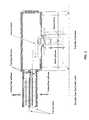
- FIG. 3is a side view of double dual slot load lock and transfer chamber construction in system AKT Gen4.
- FIG. 4is a schematic drawing demonstrating loading and unloading of a pre-processed substrate using the double dual slot load lock, wherein the substrate is loaded from ACLS to the upper load lock, and then unloaded to the transfer chamber through the lower load lock.
- FIG. 5is a schematic drawing demonstrating loading and unloading of a pre-processed substrate using the double dual slot load lock, wherein the substrate is loaded from ACLS to the lower load lock, and then unloaded to the transfer chamber through the upper load lock.
- FIG. 6is a schematic drawing demonstrating loading and unloading of a processed substrate using the double dual slot load lock, wherein the substrate is loaded from the transfer chamber to the lower load lock, and then unloaded to ACLS through the upper load lock.
- FIG. 7is a schematic drawing demonstrating pumping and venting processes which take place in the double dual slot load lock. Specifically, filtered diffuser N 2 vent is used for cooling a processed substrate when venting.
- FIGS. 8A-8Cshow system size comparison among AKT5500 (state-of-art system) ( Figure A), AKT stretch (Figure B), and AKT Gen4 ( Figure C).
- the AKT stretchis 133% stretch of AKT5500 and a traditional approach to AKT Gen4.
- Both AKT5500 and AKT stretchhave two dual slot load locks which are constructed at two locations, whereas AKT Gen 4 has one double dual slot load lock.
- a semiconductor wafer processing systemcomprising a cassette load station 101 , load lock chamber 102 , a central transfer chamber 103 , one or more process chambers 104 , a heat chamber 105 , and control towers and gas chamber 106 (FIG. 1 ).
- the load lock chamber 102is provided for transferring wafers between the transfer chamber 103 , which is typically at high vacuum, and the outside, typically a clean room at atmospheric pressure.
- the central transfer chamber 103is provided with a vacuum transfer robot located therein for transferring wafers between the load lock chamber 102 and the process chambers 104 /heat chamber 105 , which, are located about the periphery of the transfer chamber 103 .
- FIG. 2is an over view of the system with substrate transferring link 107 .
- the load lock chamber 102comprises double dual slot load lock constructed at one body (i.e., one location, in one chamber).
- Each load lockhas dual slot load lock (DSL) function: upper slot for loading pre-processed substrate from cassette load station 101 (atmospheric side); and lower slot for unloading processed substrate to cassette load station 101 (atmospheric side).
- DSLdual slot load lock
- the substrateis a wafer or a glass substrate.
- Vacuum robot in the central transfer chamber 103passes substrates through slit valves in the various connected processing chambers 104 or heater chamber 105 and retrieves them after processing in the chambers is complete. Access between the individual process chambers 104 and between the transfer chamber 103 and the load lock chamber 102 is via flip door type slit valves which selectively isolate the process chambers 104 or heat chamber 105 from the robot (in transfer chamber 103 ) and the robot from the load lock chamber 102 .
- the load lock chamber at the atmospheric sidemay have other than flip door type slit valves. Other doors may also be used to separate the vacuum condition in the load lock chamber from the atmospheric condition outside the chamber.
- FIG. 3is a system side view showing the construction of double dual slot load lock and the transfer chamber.
- the flip type valveis closed from the atmospheric side, which makes it possible to keep load lock vacuum condition with small torque actuator.
- the valveis always operated below the substrate transferring plane to reduce particle exposure and opens before loading and unloading of a substrate.
- This system configurationpermits processing in one or more chambers while wafers are being loaded or unloaded at other process chambers or at the load lock chamber and permits wafer transfer from one processing chamber to another via the transfer chamber.
- Different processesmay be simultaneously performed on different substrates at different process chambers.
- Each wafer which is dispensed from load lockmay be stepped through the same process steps to produce the same type of wafer.
- different wafers from the same load lockmay be programmed to undergo a different “recipe” involving different steps and/or process times, such that different types of wafers are produced.
- the vacuum robotwas operated by Z-drive in an up-and-down motion.
- the Z-drive shaftis a vacuum seal constructed in chambers with nitrogen purge and vacuum at the same time.
- pre-processed substratesare loaded into the upper slot in one of the load locks from the cassette load station (FIGS. 4 - 5 ).
- the upper slotoptionally has a heating plate for heating up the substrates.
- the heating plateis either a stationary plate or a moving plate. It can approximate to the substrates by Z drive to increase the heating efficiency.
- the heating temperaturecan be up to 400° C.
- the heated substratesare then unloaded from the other load lock to the transfer chamber, and further to the process chambers for processing, or to the heat chamber for either preheating or annealing.
- Lower slothas a cooling plate for cooling down the processed substrates.
- the cooling plateis either a stationary plate or moving plate and it can approximate to the substrates by Z drive to increase the cooling efficiency.
- a small amount of helium gas (He)can be supplied with nitrogen gas (N 2 ) for cooling.
- Filtered diffuser N 2 ventis used to prevent particle generation in the load locks (FIG. 7 ).
- the temperaturecan be cooled down from 350° C. to 80° C.
- each load lockloads and unloads substrates separately. Normally, one is venting and the other is pumping so that the vacuum pump can be shared between the two load locks.
- the double dual slot load lock (DDSL) system disclosed hereinprovides several advantages in comparison with traditional one DSL system, such as AKT5500 or AKT stretch (FIGS. 8 A- 8 C).
- constructing two dual slot load lock at one body (one location)can increase system cost performance, i.e., minimize system footprint and increase system throughput that was restricted by the load lock pumping/venting activity.
- the system maximum throughput determined by the load lock activityis approximately 30 substrate/hour.
- the system maximum throughputis approximately 60 substrate/hour.
- a single layer firm (passivation) processhas a throughput of approximately 26 substrate/hour for traditional one DSL system, while for one embodiment of the double dual slot load lock system disclosed herein, the passivation process has a throughput of approximately 50 substrate/hour. Since the throughput is restricted by load lock activity, a traditional one DSL system with 3 process chambers has the same throughput as the one with 4 process chambers. For active layer process, a traditional one DSL system (with 4 process chambers) has a throughput of approximately 18 substrate/hour, the same as for one embodiment of the double dual slot load lock system disclosed herein. In this case, the system throughput is the same for both one and double DSL systems, therefore system can use one of the two dual slot load lock. Most customers prefer a system that is capable of switching the process based on the production situation, therefore the system has to be configured to handle quick process. For example, the system can be configured to have shorter process time, or change process time based on process data.
- the double dual slot load lock systemrequires narrower atmospheric cassette load station than two DSL systems. For grand transportation, there is an equipment size limitation of approximate 3.0 m in dimension.
- the transfer chamberis designed in a shape of heptagon and the maximum process chamber quantity is 5. To meet the same size requirement, for two DSL systems, the maximum process chamber quantity would be 3.
- a substrate processing systemwhich comprises a cassette load station, a load lock chamber, a transfer chamber, and one or more process chambers.
- the transfer chamberis centrally located, and the multiple process chambers are located about the periphery of the transfer chamber.
- the load lock chambercomprises two dual slot load lock constructed at one location.
- each dual slot load lockhas a heating plate and a cooling plate located in different slots.
- the heating plateis a stationary plate or moving plate operated by Z-drive, and can heat the temperature up to 400° C. during pumping.
- the cooling plateis a stationary plate or moving plate operated by Z-drive, and can cool the temperature down from about 350° C. to about 80° C. during venting. More specifically, the cooling is achieved by water or by venting using nitrogen gas mixed with helium.
- the substrate processing system described hereinmay further comprise a vacuum robot, which is located in the transfer chamber for transferring substrates.
- the vacuum robotis operated by Z-drive.
- the systemmay further comprise a flip type door located between the cassette load station and the load lock chamber.
- Flip type slit valvesmay also be constructed between the load lock chamber and the transfer chamber. Such slit valves are closed from atmospheric side and always operated below substrate transferring plane to reduce particle exposure.
- the substrate processing systemmay further comprise filter diffusers, which are located in the both dual slot load locks to prevent particle generation.
- This methodcomprises the steps of moving substrates from the cassette load station to the transfer chamber through the load lock chamber; transferring the substrates from the transfer chamber to the process chambers; processing the substrates in the process chambers; and unloading the processed substrates from the process chambers to the cassette load station through the load lock chamber.
- one of the dual slot load locksis in a vacuum condition for unloading pre-processed substrates from the load lock chamber to the transfer chamber, whereas at the same time the other dual slot load lock is in an atmospheric condition for unloading processed substrates from the load lock chamber to the cassette load station.
- the pre-processed substratesare heated up to about 400° C. before loading to the transfer chamber.
- the heated substratesare then transferred to the transfer chamber by a vacuum robot which is driven by Z-drive.
- the processed substratesare cooled down from about 350° C. to about 80° C. before loading to the cassette load station.
- a small amount of helium gasis supplied with nitrogen gas.
- the coolingcan be achieved by water.
- one load lockis in a vacuum condition and at the same time, the other load lock is in an atmospheric/venting condition.
- One vacuum pumpis shared between the two load locks.
- filter diffusersare located on both load locks to prevent particle generation. Increased vent speed may also be used to further prevent particle generation.
- the system/method disclosed hereinprovides an improved wafer support and transport means to enable automatic and repetitive moving of individual wafers into and from load locks into, through and between processing chambers while minimizing damage and contamination of wafers. Additionally, using two dual slot load lock constructed in the same chamber increases system cost performance, i.e., minimizes system footprint and increases system throughput that was restricted by the load lock pumping/venting activity.
Landscapes
- Engineering & Computer Science (AREA)
- Physics & Mathematics (AREA)
- Condensed Matter Physics & Semiconductors (AREA)
- General Physics & Mathematics (AREA)
- Manufacturing & Machinery (AREA)
- Computer Hardware Design (AREA)
- Microelectronics & Electronic Packaging (AREA)
- Power Engineering (AREA)
- Robotics (AREA)
- Container, Conveyance, Adherence, Positioning, Of Wafer (AREA)
Abstract
Description
This is a divisional application of U.S. Ser. No. 09/663,862 filed on Sep. 15, 2000.
1. Field of the Invention
The present invention relates generally to the fields of semiconductor manufacturing. More specifically, the present invention relates to a semiconductor wafer or glass substrate processing system comprising a double dual slot load lock and uses thereof.
2. Description of the Related Art
The need for greater throughput and yield in the manufacture of semiconductor devices has driven the development and use of more highly automated wafer processing machines. Also, the desire to minimize wafer particulate contamination during processing has led to the use of vacuum load locks and wafer transport mechanisms which operate in vacuum.
In continuous throughput systems, wafers must be introduced into the vacuum chamber through a load lock in order to prevent exposing the vacuum condition in the chamber to the air outside the chamber. When a wafer is to be loaded into the chamber, the inner closure means, such as a sealing plate, is activated to seal the inner side of the opening, and then the outer closure means, such as a sealing door, is opened. Next the door is opened, a wafer is inserted through the opening, and the door is again closed. The load lock chamber now containing the wafer is pumped down to contain an atmosphere compatible with the atmosphere in the processing vacuum chamber, and then the inner sealing plate is moved away from the opening to expose the wafer for processing in the main vacuum chamber. To increase the throughout, some systems employ two load lock chambers so that processing of wafers can continue uninterrupted by a delay caused by the need to open, empty, reload and re-equilibrate a single load lock chamber.
Despite the increased vacuum isolation, the state-of-the-art systems typically have difficulty providing commercially acceptable throughput for high vacuum processes. Presently, typical load lock chambers employ sliding or rotating valves to isolate a single wafer. Such load locks require a pumpdown cycle for each wafer processed and thus inhibit throughput. In addition, the load locks are typically in-line devices; that is, wafers pass in a straight line through the load lock. This substantially contributes to the overall width of the wafer processing machine. Furthermore, in the prior art designs, mechanical feedthroughs, which are used to transmit motion through a vacuum seal, have not been adequate to the task of simultaneously operating a load lock valve and indexing an internal wafer cassette.
Therefore, the prior art is deficient in the lack of effective system/means of processing substrates in a high throughput fashion and meanwhile minimizing particulate contamination during processing. Specifically, the prior art is deficient in the lack of a highly automated substrate processing system comprising double dual slot load locks constructed at one body. The present invention fulfills this long-standing need and desire in the art.
In one aspect of the present invention, there is provided a substrate processing system, which comprises a cassette load station; a load lock chamber; a centrally located transfer chamber; and one or more process chambers located about the periphery of the transfer chamber. In this system, the load lock chamber comprises two dual slot load locks constructed at same location.
In another aspect of the present invention, there is provided a method of processing substrates in the system disclosed herein for semiconductor manufacturing. This method comprises the following steps: first, moving substrates from the cassette load station to the transfer chamber through the load lock chamber; secondly, transferring the substrates from the transfer chamber to the process chambers; thirdly, processing the substrates in the process chambers; and lastly, unloading the processed substrates from the process chambers to the same cassette load station through the same load lock chamber. In this method, one load lock is in a vacuum condition and the other load lock is in an atmospheric/venting condition at the same time.
Other and further aspects, features, and advantages of the present invention will be apparent from the following description of the embodiments of the invention given for the purpose of disclosure.
So that the matter in which the above-recited features, advantages and objects of the invention, as well as others which will become clear, are attained and can be understood in detail, more particular descriptions of the invention briefly summarized above may be had by reference to certain embodiments thereof which are illustrated in the appended drawings. These drawings form a part of the specification. It is to be noted, however, that the appended drawings illustrate embodiments of the invention and therefore are not to be considered limiting in their scope.
Provided herein is a semiconductor wafer processing system, comprising acassette load station 101,load lock chamber 102, acentral transfer chamber 103, one ormore process chambers 104, aheat chamber 105, and control towers and gas chamber106 (FIG.1).
Theload lock chamber 102 is provided for transferring wafers between thetransfer chamber 103, which is typically at high vacuum, and the outside, typically a clean room at atmospheric pressure. Thecentral transfer chamber 103 is provided with a vacuum transfer robot located therein for transferring wafers between theload lock chamber 102 and theprocess chambers 104/heat chamber 105, which, are located about the periphery of thetransfer chamber 103.FIG. 2 is an over view of the system withsubstrate transferring link 107.
Specifically, theload lock chamber 102 comprises double dual slot load lock constructed at one body (i.e., one location, in one chamber). Each load lock has dual slot load lock (DSL) function: upper slot for loading pre-processed substrate from cassette load station101 (atmospheric side); and lower slot for unloading processed substrate to cassette load station101 (atmospheric side). In most cases, the substrate is a wafer or a glass substrate.
Substrates are loaded/unloaded by both vacuum robot and atmospheric robot. Vacuum robot in thecentral transfer chamber 103 passes substrates through slit valves in the various connectedprocessing chambers 104 orheater chamber 105 and retrieves them after processing in the chambers is complete. Access between theindividual process chambers 104 and between thetransfer chamber 103 and theload lock chamber 102 is via flip door type slit valves which selectively isolate theprocess chambers 104 orheat chamber 105 from the robot (in transfer chamber103) and the robot from theload lock chamber 102. However, the load lock chamber at the atmospheric side may have other than flip door type slit valves. Other doors may also be used to separate the vacuum condition in the load lock chamber from the atmospheric condition outside the chamber.
This system configuration permits processing in one or more chambers while wafers are being loaded or unloaded at other process chambers or at the load lock chamber and permits wafer transfer from one processing chamber to another via the transfer chamber. Different processes may be simultaneously performed on different substrates at different process chambers. Each wafer which is dispensed from load lock may be stepped through the same process steps to produce the same type of wafer. Alternatively, different wafers from the same load lock may be programmed to undergo a different “recipe” involving different steps and/or process times, such that different types of wafers are produced.
Specifically, the vacuum robot was operated by Z-drive in an up-and-down motion. The Z-drive shaft is a vacuum seal constructed in chambers with nitrogen purge and vacuum at the same time.
The above-disclosed system can be used for processing substrates for semiconductor manufacturing. In more specific detail, pre-processed substrates are loaded into the upper slot in one of the load locks from the cassette load station (FIGS.4-5). The upper slot optionally has a heating plate for heating up the substrates. The heating plate is either a stationary plate or a moving plate. It can approximate to the substrates by Z drive to increase the heating efficiency. During pumping, the heating temperature can be up to 400° C. The heated substrates are then unloaded from the other load lock to the transfer chamber, and further to the process chambers for processing, or to the heat chamber for either preheating or annealing.
After processing in the chambers is complete, the processed substrates are then unloaded from the lower slot in one of the load locks to the cassette load station (FIG.6). Lower slot has a cooling plate for cooling down the processed substrates. The cooling plate is either a stationary plate or moving plate and it can approximate to the substrates by Z drive to increase the cooling efficiency. Also, a small amount of helium gas (He) can be supplied with nitrogen gas (N2) for cooling. Filtered diffuser N2vent is used to prevent particle generation in the load locks (FIG.7). During venting, the temperature can be cooled down from 350° C. to 80° C. When operated, each load lock loads and unloads substrates separately. Normally, one is venting and the other is pumping so that the vacuum pump can be shared between the two load locks.
The double dual slot load lock (DDSL) system disclosed herein provides several advantages in comparison with traditional one DSL system, such as AKT5500 or AKT stretch (FIGS.8A-8C). First, constructing two dual slot load lock at one body (one location) can increase system cost performance, i.e., minimize system footprint and increase system throughput that was restricted by the load lock pumping/venting activity. For a traditional one dual slot load lock system (with 4 process chambers), the system maximum throughput determined by the load lock activity is approximately 30 substrate/hour. In contrast, for one embodiment of the double dual slot load lock system disclosed herein, the system maximum throughput is approximately 60 substrate/hour. For example, a single layer firm (passivation) process has a throughput of approximately 26 substrate/hour for traditional one DSL system, while for one embodiment of the double dual slot load lock system disclosed herein, the passivation process has a throughput of approximately 50 substrate/hour. Since the throughput is restricted by load lock activity, a traditional one DSL system with 3 process chambers has the same throughput as the one with 4 process chambers. For active layer process, a traditional one DSL system (with 4 process chambers) has a throughput of approximately 18 substrate/hour, the same as for one embodiment of the double dual slot load lock system disclosed herein. In this case, the system throughput is the same for both one and double DSL systems, therefore system can use one of the two dual slot load lock. Most customers prefer a system that is capable of switching the process based on the production situation, therefore the system has to be configured to handle quick process. For example, the system can be configured to have shorter process time, or change process time based on process data.
Another advantage of using the presently disclosed double dual slot load lock system is its compact size. The double dual slot load lock system requires narrower atmospheric cassette load station than two DSL systems. For grand transportation, there is an equipment size limitation of approximate 3.0 m in dimension. In one embodiment of the double dual slot load lock system, the transfer chamber is designed in a shape of heptagon and the maximum process chamber quantity is 5. To meet the same size requirement, for two DSL systems, the maximum process chamber quantity would be 3.
Therefore, a substrate processing system is hereby provided, which comprises a cassette load station, a load lock chamber, a transfer chamber, and one or more process chambers. The transfer chamber is centrally located, and the multiple process chambers are located about the periphery of the transfer chamber. The load lock chamber comprises two dual slot load lock constructed at one location.
Specifically, each dual slot load lock has a heating plate and a cooling plate located in different slots. The heating plate is a stationary plate or moving plate operated by Z-drive, and can heat the temperature up to 400° C. during pumping. Similarly, the cooling plate is a stationary plate or moving plate operated by Z-drive, and can cool the temperature down from about 350° C. to about 80° C. during venting. More specifically, the cooling is achieved by water or by venting using nitrogen gas mixed with helium.
The substrate processing system described herein may further comprise a vacuum robot, which is located in the transfer chamber for transferring substrates. The vacuum robot is operated by Z-drive. Still, the system may further comprise a flip type door located between the cassette load station and the load lock chamber. Flip type slit valves may also be constructed between the load lock chamber and the transfer chamber. Such slit valves are closed from atmospheric side and always operated below substrate transferring plane to reduce particle exposure. Still yet, the substrate processing system may further comprise filter diffusers, which are located in the both dual slot load locks to prevent particle generation.
Further provided is a method of processing substrates using the above-disclosed system for semiconductor manufacturing. This method comprises the steps of moving substrates from the cassette load station to the transfer chamber through the load lock chamber; transferring the substrates from the transfer chamber to the process chambers; processing the substrates in the process chambers; and unloading the processed substrates from the process chambers to the cassette load station through the load lock chamber. In this method, one of the dual slot load locks is in a vacuum condition for unloading pre-processed substrates from the load lock chamber to the transfer chamber, whereas at the same time the other dual slot load lock is in an atmospheric condition for unloading processed substrates from the load lock chamber to the cassette load station.
Furthermore, the pre-processed substrates are heated up to about 400° C. before loading to the transfer chamber. The heated substrates are then transferred to the transfer chamber by a vacuum robot which is driven by Z-drive. After processing, the processed substrates are cooled down from about 350° C. to about 80° C. before loading to the cassette load station. To increase cooling efficiency, a small amount of helium gas is supplied with nitrogen gas. Alternatively, the cooling can be achieved by water.
In this method, one load lock is in a vacuum condition and at the same time, the other load lock is in an atmospheric/venting condition. One vacuum pump is shared between the two load locks. Additionally, filter diffusers are located on both load locks to prevent particle generation. Increased vent speed may also be used to further prevent particle generation.
The system/method disclosed herein provides an improved wafer support and transport means to enable automatic and repetitive moving of individual wafers into and from load locks into, through and between processing chambers while minimizing damage and contamination of wafers. Additionally, using two dual slot load lock constructed in the same chamber increases system cost performance, i.e., minimizes system footprint and increases system throughput that was restricted by the load lock pumping/venting activity.
Any patents or publications mentioned in this specification are indicative of the levels of those skilled in the art to which the invention pertains. These patents and publications are herein incorporated by reference to the same extent as if each individual publication was specifically and individually indicated to be incorporated by reference.
One skilled in the art will readily appreciate that the present invention is well adapted to carry out the objects and obtain the ends and advantages mentioned, as well as those inherent therein. It will be apparent to those skilled in the art that various modifications and variations can be made in practicing the present invention without departing from the spirit or scope of the invention. Changes therein and other uses will occur to those skilled in the art which are encompassed within the spirit of the invention as defined by the scope of the claims.
Claims (25)
1. A substrate processing system, comprising:
a cassette load station;
a transfer chamber;
a load lock chamber located between the cassette load station and the transfer chamber, the load lock chamber having a substrate temperature regulating device movably disposed therein, wherein the load lock chamber comprises upper and lower isolated load lock regions that share a common wall, the upper and lower isolated load lock regions each comprising a sealable opening to the cassette load station and a sealable opening to the transfer chamber, the upper and lower isolated load lock regions each comprising at least two substrate storage slots; and
one or more process chambers located about the periphery of the transfer chamber, each of the one or more process chambers comprising an opening to the transfer chamber.
2. The substrate processing system ofclaim 1 , wherein the temperature regulating device comprises a heating plate.
3. The substrate processing system ofclaim 1 , wherein the temperature regulating device comprises a cooling plate.
4. The substrate processing system ofclaim 1 , further comprising
a robot diposed in the transfer chamber for moving substrates between the load lock chamber and the transfer chamber.
5. The substrate processing system ofclaim 4 , wherein the robot is vertically movable.
6. A substrate processing system, comprising:
a cassette load station;
a transfer chamber;
a load lock chamber located between the cassette load station and the transfer chamber, the load lock chamber having a substrate temperature regulating device movably disposed therein, wherein the load lock chamber comprises upper and lower isolated load lock regions, wherein each of the upper and lower isolated load lock regions comprises a cooling plate and two substrate storage slots, the upper and lower isolated load lock regions each comprising an opening to the cassette load station and an opening to the transfer chamber; and
one or more process chambers located about the periphery of the transfer chamber, each of the one or more process chambers comprising an opening to the transfer chamber.
7. The substrate processing system of theclaim 6 , further comprising a robot disposed in the transfer chamber for moving substrates between the load lock chamber and the transfer chamber.
8. The substrate processing system ofclaim 7 , wherein the robot is vertically movable.
9. The substrate processing system ofclaim 6 , further comprising a flip type door between the cassette load station and the load lock chamber.
10. The substrate processing system ofclaim 6 , further comprising a flip type slit valve between the load lock chamber and the transfer chamber.
11. The substrate processing system ofclaim 10 , wherein the valve is operated below a substrate transferring plane.
12. A substrate processing system, comprising:
a cassette load station;
a transfer chamber;
a load lock chamber located between the cassette load station and the transfer chamber, wherein the load lock chamber comprises upper and lower isolated load lock regions each having two substrate storage slots, a heating plate in each isolated load lock region, wherein at least one of the heating plate or coolin plate is moveable, the upper and lower isolated load lock regions each comprising an opening to the cassette load station and an opening to the transfer chamber; and
one or more process chambers located about the periphery of the transfer chamber, each of the one or more process chambers comprising an opening to the transfer chamber.
13. The substrate processing system ofclaim 12 , wherein the upper and lower isolated load lock regions share a common wall.
14. The substrate processing system ofclaim 12 , further comprising a vertically movable robot disposed in the transfer chamber for moving substrates between the load lock chamber and the transfer chamber.
15. The substrate processing system ofclaim 12 , further comprising a flip type door between the load lock chamber and the transfer chamber.
16. The substrate processing system ofclaim 12 , further comprising a flip type slit valve between the load lock chamber and the transfer chamber.
17. The substrate processing system ofclaim 16 , wherein the valve is operated below a substrate transferring plane.
18. A substrate processing system, comprising:
a transfer chamber;
a load lock chamber located between the cassette load station and the transfer chamber, the load lock chamber having a substrate temperature regulating movably device disposed therein, wherein the load lock chamber comprises upper and lower isolated load lock regions that share a common wall, the upper and lower isolated load lock regions each comprising two substrate storage slots, a sealable opening to a cassette load station and a sealable opening to the transfer chamber; and
one or more process chambers located about the periphery of the transfer chamber, each of the one or more process chambers comprising an opening to the transfer chamber.
19. The substrate processing system ofclaim 18 , wherein the substrate temperature regulating device is a heating plate.
20. The substrate processing system ofclaim 18 , wherein the substrate temperature regulating device is a cooling plate.
21. The substrate processing system ofclaim 18 , further comprising a robot disposed in the transfer chamber for moving substrates between the load lock chamber and the transfer chamber.
22. The substrate processing system ofclaim 21 , wherein the robot is vertically movable.
23. A substrate processing system, comprising:
a transfer chamber;
a load lock chamber located between the cassette load station and the transfer chamber, the load lock chamber having a substrate temperature regulating device movably disposed therein, wherein the load lock chamber comprises upper and lower isolated load lock regions, wherein each of the upper and lower isolated load lock regions comprises a cooling plate and two substrate storage slots, the upper and lower isolated load lock regions each comprising an opening to a cassette load station and an opening to the transfer chamber; and
one or more process chambers located about the periphery of the transfer chamber, each of the one or more process chambers comprising an opening to the transfer chamber.
24. The substrate processing system ofclaim 23 , further comprising a robot disposed in the transfer chamber for moving substrates between the load lock chamber and the transfer chamber.
25. The substrate processing system ofclaim 24 , wherein the robot is vertically movable.
Priority Applications (3)
| Application Number | Priority Date | Filing Date | Title |
|---|---|---|---|
| US09/957,784US7105463B2 (en) | 2000-09-15 | 2001-09-21 | Load lock chamber having two dual slot regions |
| US11/278,318US7316966B2 (en) | 2001-09-21 | 2006-03-31 | Method for transferring substrates in a load lock chamber |
| US11/926,720US8616820B2 (en) | 2001-09-21 | 2007-10-29 | Double dual slot load lock chamber |
Applications Claiming Priority (2)
| Application Number | Priority Date | Filing Date | Title |
|---|---|---|---|
| US66386200A | 2000-09-15 | 2000-09-15 | |
| US09/957,784US7105463B2 (en) | 2000-09-15 | 2001-09-21 | Load lock chamber having two dual slot regions |
Related Parent Applications (1)
| Application Number | Title | Priority Date | Filing Date |
|---|---|---|---|
| US66386200ADivision | 2000-09-15 | 2000-09-15 |
Related Child Applications (1)
| Application Number | Title | Priority Date | Filing Date |
|---|---|---|---|
| US11/278,318DivisionUS7316966B2 (en) | 2001-09-21 | 2006-03-31 | Method for transferring substrates in a load lock chamber |
Publications (2)
| Publication Number | Publication Date |
|---|---|
| US20020034886A1 US20020034886A1 (en) | 2002-03-21 |
| US7105463B2true US7105463B2 (en) | 2006-09-12 |
Family
ID=24663546
Family Applications (1)
| Application Number | Title | Priority Date | Filing Date |
|---|---|---|---|
| US09/957,784Expired - LifetimeUS7105463B2 (en) | 2000-09-15 | 2001-09-21 | Load lock chamber having two dual slot regions |
Country Status (6)
| Country | Link |
|---|---|
| US (1) | US7105463B2 (en) |
| EP (1) | EP1319243A2 (en) |
| JP (1) | JP2004523880A (en) |
| KR (4) | KR20080109062A (en) |
| TW (1) | TW512421B (en) |
| WO (1) | WO2002023597A2 (en) |
Cited By (22)
| Publication number | Priority date | Publication date | Assignee | Title |
|---|---|---|---|---|
| WO2006086665A3 (en)* | 2005-02-09 | 2007-06-14 | Multibeam Systems Inc | Multiple loadlocks and processing chamber |
| US20080138177A1 (en)* | 2003-03-11 | 2008-06-12 | Asml Netherlands B.V. | Load lock and method for transferring objects |
| US20090092466A1 (en)* | 2006-06-15 | 2009-04-09 | Applied Materials, Inc. | Multi-level load lock chamber, transfer chamber, and robot suitable for interfacing with same |
| US20090114153A1 (en)* | 2007-11-01 | 2009-05-07 | Applied Materials, Inc. | Method and apparatus for sealing an opening of a processing chamber |
| US20090142167A1 (en)* | 2007-11-30 | 2009-06-04 | Novellus Systems, Inc. | Loadlock designs and methods for using same |
| US7576831B2 (en) | 2003-03-11 | 2009-08-18 | Asml Netherlands B.V. | Method and apparatus for maintaining a machine part |
| US20100107672A1 (en)* | 1999-12-15 | 2010-05-06 | Applied Materials, Inc. | Dual substrate loadlock process equipment |
| US20100236476A1 (en)* | 2009-02-22 | 2010-09-23 | Mapper Lithography Ip B.V. | Substrate Support Structure, Clamp Preparation Unit, and Lithography System |
| US20100270004A1 (en)* | 2005-05-12 | 2010-10-28 | Landess James D | Tailored profile pedestal for thermo-elastically stable cooling or heating of substrates |
| CN101256933B (en)* | 2007-03-02 | 2011-06-08 | Asm日本子公司 | Cluster type semiconductor processing apparatus |
| US7960297B1 (en) | 2006-12-07 | 2011-06-14 | Novellus Systems, Inc. | Load lock design for rapid wafer heating |
| US8033771B1 (en)* | 2008-12-11 | 2011-10-11 | Novellus Systems, Inc. | Minimum contact area wafer clamping with gas flow for rapid wafer cooling |
| US8137465B1 (en) | 2005-04-26 | 2012-03-20 | Novellus Systems, Inc. | Single-chamber sequential curing of semiconductor wafers |
| US8282768B1 (en) | 2005-04-26 | 2012-10-09 | Novellus Systems, Inc. | Purging of porogen from UV cure chamber |
| US8288288B1 (en) | 2008-06-16 | 2012-10-16 | Novellus Systems, Inc. | Transferring heat in loadlocks |
| US8371567B2 (en) | 2011-04-13 | 2013-02-12 | Novellus Systems, Inc. | Pedestal covers |
| US8616820B2 (en)* | 2001-09-21 | 2013-12-31 | Applied Materials, Inc. | Double dual slot load lock chamber |
| US8920162B1 (en) | 2007-11-08 | 2014-12-30 | Novellus Systems, Inc. | Closed loop temperature heat up and control utilizing wafer-to-heater pedestal gap modulation |
| US9145611B2 (en) | 2012-09-07 | 2015-09-29 | Applied Materials, Inc. | Load lock chamber with slit valve doors |
| US9835388B2 (en) | 2012-01-06 | 2017-12-05 | Novellus Systems, Inc. | Systems for uniform heat transfer including adaptive portions |
| US10347547B2 (en) | 2016-08-09 | 2019-07-09 | Lam Research Corporation | Suppressing interfacial reactions by varying the wafer temperature throughout deposition |
| US20220081757A1 (en)* | 2020-09-11 | 2022-03-17 | Tokyo Electron Limited | Film forming apparatus, film forming system, and film forming method |
Families Citing this family (42)
| Publication number | Priority date | Publication date | Assignee | Title |
|---|---|---|---|---|
| WO2002023597A2 (en) | 2000-09-15 | 2002-03-21 | Applied Materials, Inc. | Double dual slot load lock for process equipment |
| US7129694B2 (en)* | 2002-05-23 | 2006-10-31 | Applied Materials, Inc. | Large substrate test system |
| DE10227332A1 (en)* | 2002-06-19 | 2004-01-15 | Akt Electron Beam Technology Gmbh | Control device with improved test properties |
| US8545159B2 (en)* | 2003-10-01 | 2013-10-01 | Jusung Engineering Co., Ltd. | Apparatus having conveyor and method of transferring substrate using the same |
| US7207766B2 (en)* | 2003-10-20 | 2007-04-24 | Applied Materials, Inc. | Load lock chamber for large area substrate processing system |
| US7355418B2 (en)* | 2004-02-12 | 2008-04-08 | Applied Materials, Inc. | Configurable prober for TFT LCD array test |
| US6833717B1 (en) | 2004-02-12 | 2004-12-21 | Applied Materials, Inc. | Electron beam test system with integrated substrate transfer module |
| US20060038554A1 (en)* | 2004-02-12 | 2006-02-23 | Applied Materials, Inc. | Electron beam test system stage |
| US7497414B2 (en)* | 2004-06-14 | 2009-03-03 | Applied Materials, Inc. | Curved slit valve door with flexible coupling |
| US7075323B2 (en)* | 2004-07-29 | 2006-07-11 | Applied Materials, Inc. | Large substrate test system |
| US7467916B2 (en)* | 2005-03-08 | 2008-12-23 | Asm Japan K.K. | Semiconductor-manufacturing apparatus equipped with cooling stage and semiconductor-manufacturing method using same |
| JP4860167B2 (en)* | 2005-03-30 | 2012-01-25 | 東京エレクトロン株式会社 | Load lock device, processing system, and processing method |
| JP4619854B2 (en) | 2005-04-18 | 2011-01-26 | 東京エレクトロン株式会社 | Load lock device and processing method |
| US7535238B2 (en)* | 2005-04-29 | 2009-05-19 | Applied Materials, Inc. | In-line electron beam test system |
| US20060273815A1 (en)* | 2005-06-06 | 2006-12-07 | Applied Materials, Inc. | Substrate support with integrated prober drive |
| US20070006936A1 (en)* | 2005-07-07 | 2007-01-11 | Applied Materials, Inc. | Load lock chamber with substrate temperature regulation |
| TWI295816B (en)* | 2005-07-19 | 2008-04-11 | Applied Materials Inc | Hybrid pvd-cvd system |
| US7845891B2 (en) | 2006-01-13 | 2010-12-07 | Applied Materials, Inc. | Decoupled chamber body |
| JP5829376B2 (en)* | 2006-03-14 | 2015-12-09 | アプライド マテリアルズ インコーポレイテッドApplied Materials,Incorporated | Method for reducing crosstalk in multi-column electron beam inspection system |
| US7602199B2 (en)* | 2006-05-31 | 2009-10-13 | Applied Materials, Inc. | Mini-prober for TFT-LCD testing |
| US7786742B2 (en)* | 2006-05-31 | 2010-08-31 | Applied Materials, Inc. | Prober for electronic device testing on large area substrates |
| US7665951B2 (en)* | 2006-06-02 | 2010-02-23 | Applied Materials, Inc. | Multiple slot load lock chamber and method of operation |
| US7845618B2 (en) | 2006-06-28 | 2010-12-07 | Applied Materials, Inc. | Valve door with ball coupling |
| US8124907B2 (en)* | 2006-08-04 | 2012-02-28 | Applied Materials, Inc. | Load lock chamber with decoupled slit valve door seal compartment |
| US8920097B2 (en)* | 2006-11-02 | 2014-12-30 | Globalfoundries Singapore Pte. Ltd. | Wafer handling system for a loadlock |
| US20080251019A1 (en)* | 2007-04-12 | 2008-10-16 | Sriram Krishnaswami | System and method for transferring a substrate into and out of a reduced volume chamber accommodating multiple substrates |
| TW200908363A (en)* | 2007-07-24 | 2009-02-16 | Applied Materials Inc | Apparatuses and methods of substrate temperature control during thin film solar manufacturing |
| IL188155A0 (en)* | 2007-12-16 | 2008-11-03 | Nova Measuring Instr Ltd | Measurement system |
| GB2469112A (en) | 2009-04-03 | 2010-10-06 | Mapper Lithography Ip Bv | Wafer support using controlled capillary liquid layer to hold and release wafer |
| JP5670351B2 (en) | 2009-02-22 | 2015-02-18 | マッパー・リソグラフィー・アイピー・ビー.ブイ. | Preparation unit for lithography machine |
| WO2010105967A2 (en)* | 2009-03-18 | 2010-09-23 | Oc Oerlikon Balzers Ag | Vacuum treatment apparatus |
| US8481355B2 (en)* | 2009-12-15 | 2013-07-09 | Primestar Solar, Inc. | Modular system and process for continuous deposition of a thin film layer on a substrate |
| TWI514089B (en) | 2011-04-28 | 2015-12-21 | Mapper Lithography Ip Bv | Apparatus for transferring a substrate in a lithography system |
| US20160314997A1 (en)* | 2015-04-22 | 2016-10-27 | Applied Materials, Inc. | Loadlock apparatus, cooling plate assembly, and electronic device processing systems and methods |
| CN106298583B (en)* | 2015-05-27 | 2019-12-03 | 中微半导体设备(上海)股份有限公司 | Processing chamber, processing chamber and vacuum lock combination and substrate handling system |
| KR101999838B1 (en) | 2015-08-11 | 2019-07-15 | 삼성디스플레이 주식회사 | Substrate processing system |
| JP6270952B1 (en)* | 2016-09-28 | 2018-01-31 | 株式会社日立国際電気 | Substrate processing apparatus, semiconductor device manufacturing method, and recording medium. |
| WO2018171908A1 (en)* | 2017-03-21 | 2018-09-27 | Applied Materials, Inc. | Apparatus for loading a substrate in a vacuum processing system, system for processing a substrate, and method for loading a substrate |
| CN106931759B (en)* | 2017-05-09 | 2022-09-09 | 南京中电熊猫液晶材料科技有限公司 | Drying device for outlet glass substrate of cleaning machine |
| KR20250057069A (en) | 2018-07-17 | 2025-04-28 | 에이에스엠엘 네델란즈 비.브이. | Particle beam inspection appartus |
| JP2020017645A (en)* | 2018-07-26 | 2020-01-30 | 株式会社Kokusai Electric | Substrate processing equipment |
| KR102574308B1 (en)* | 2020-09-16 | 2023-09-05 | 세메스 주식회사 | Apparatus for treating a substrate |
Citations (155)
| Publication number | Priority date | Publication date | Assignee | Title |
|---|---|---|---|---|
| US3976330A (en) | 1975-10-01 | 1976-08-24 | International Business Machines Corporation | Transport system for semiconductor wafer multiprocessing station system |
| US4047624A (en) | 1975-10-21 | 1977-09-13 | Airco, Inc. | Workpiece handling system for vacuum processing |
| US4178113A (en) | 1977-12-05 | 1979-12-11 | Macronetics, Inc. | Buffer storage apparatus for semiconductor wafer processing |
| US4311542A (en) | 1979-02-07 | 1982-01-19 | Breveteam S.A. | Method for manufacturing a strip-shaped composite body |
| US4512391A (en) | 1982-01-29 | 1985-04-23 | Varian Associates, Inc. | Apparatus for thermal treatment of semiconductor wafers by gas conduction incorporating peripheral gas inlet |
| US4680061A (en) | 1979-12-21 | 1987-07-14 | Varian Associates, Inc. | Method of thermal treatment of a wafer in an evacuated environment |
| US4687542A (en) | 1985-10-24 | 1987-08-18 | Texas Instruments Incorporated | Vacuum processing system |
| US4693777A (en) | 1984-11-30 | 1987-09-15 | Kabushiki Kaisha Toshiba | Apparatus for producing semiconductor devices |
| US4709655A (en) | 1985-12-03 | 1987-12-01 | Varian Associates, Inc. | Chemical vapor deposition apparatus |
| US4759681A (en) | 1985-01-22 | 1988-07-26 | Nissin Electric Co. Ltd. | End station for an ion implantation apparatus |
| US4770590A (en) | 1986-05-16 | 1988-09-13 | Silicon Valley Group, Inc. | Method and apparatus for transferring wafers between cassettes and a boat |
| US4775281A (en) | 1986-12-02 | 1988-10-04 | Teradyne, Inc. | Apparatus and method for loading and unloading wafers |
| US4785962A (en) | 1987-04-20 | 1988-11-22 | Applied Materials, Inc. | Vacuum chamber slit valve |
| US4801241A (en) | 1984-03-09 | 1989-01-31 | Tegal Corporation | Modular article processing machine and method of article handling therein |
| JPS6428933U (en) | 1987-08-12 | 1989-02-21 | ||
| US4816098A (en) | 1987-07-16 | 1989-03-28 | Texas Instruments Incorporated | Apparatus for transferring workpieces |
| US4828224A (en) | 1987-10-15 | 1989-05-09 | Epsilon Technology, Inc. | Chemical vapor deposition system |
| US4836733A (en) | 1986-04-28 | 1989-06-06 | Varian Associates, Inc. | Wafer transfer system |
| US4846102A (en) | 1987-06-24 | 1989-07-11 | Epsilon Technology, Inc. | Reaction chambers for CVD systems |
| US4857689A (en) | 1988-03-23 | 1989-08-15 | High Temperature Engineering Corporation | Rapid thermal furnace for semiconductor processing |
| US4863547A (en) | 1987-05-24 | 1989-09-05 | Tazmo Co., Ltd. | Equipment for heating and cooling substrates for coating photo resist thereto |
| US4870923A (en) | 1987-06-26 | 1989-10-03 | Dainippon Screen Mfg. Co., Ltd. | Apparatus for treating the surfaces of wafers |
| US4895107A (en) | 1987-07-06 | 1990-01-23 | Kabushiki Kaisha Toshiba | Photo chemical reaction apparatus |
| US4911103A (en) | 1987-07-17 | 1990-03-27 | Texas Instruments Incorporated | Processing apparatus and method |
| US4913929A (en) | 1987-04-21 | 1990-04-03 | The Board Of Trustees Of The Leland Stanford Junior University | Thermal/microwave remote plasma multiprocessing reactor and method of use |
| US4923584A (en) | 1988-10-31 | 1990-05-08 | Eaton Corporation | Sealing apparatus for a vacuum processing system |
| JPH02152251A (en) | 1988-12-03 | 1990-06-12 | Furendotetsuku Kenkyusho:Kk | Manufacturing system of vertical-type semiconductor |
| US4952299A (en) | 1988-10-31 | 1990-08-28 | Eaton Corporation | Wafer handling apparatus |
| US4951601A (en) | 1986-12-19 | 1990-08-28 | Applied Materials, Inc. | Multi-chamber integrated process system |
| US4966519A (en) | 1985-10-24 | 1990-10-30 | Texas Instruments Incorporated | Integrated circuit processing system |
| US4989543A (en) | 1987-10-15 | 1991-02-05 | Solems (S.A.) | Process and means for producing films for use in electronics and/or optoelectronics using plasma |
| US4990047A (en) | 1988-05-24 | 1991-02-05 | Balzers Aktiengesellschaft | Vacuum apparatus |
| US5001327A (en) | 1987-09-11 | 1991-03-19 | Hitachi, Ltd. | Apparatus and method for performing heat treatment on semiconductor wafers |
| US5044871A (en) | 1985-10-24 | 1991-09-03 | Texas Instruments Incorporated | Integrated circuit processing system |
| US5060354A (en) | 1990-07-02 | 1991-10-29 | George Chizinsky | Heated plate rapid thermal processor |
| JPH03274746A (en) | 1990-03-24 | 1991-12-05 | Sony Corp | Multi-chamber device |
| JPH0498848A (en) | 1990-08-16 | 1992-03-31 | Nec Yamagata Ltd | Wafer replacing machine |
| US5131460A (en) | 1991-10-24 | 1992-07-21 | Applied Materials, Inc. | Reducing particulates during semiconductor fabrication |
| JPH04240721A (en) | 1991-01-25 | 1992-08-28 | Sony Corp | Multi chamber process device |
| US5186718A (en) | 1989-05-19 | 1993-02-16 | Applied Materials, Inc. | Staged-vacuum wafer processing system and method |
| US5187115A (en) | 1977-12-05 | 1993-02-16 | Plasma Physics Corp. | Method of forming semiconducting materials and barriers using a dual enclosure apparatus |
| US5199483A (en) | 1991-05-15 | 1993-04-06 | Applied Materials, Inc. | Method and apparatus for cooling wafers |
| JPH0513551Y2 (en) | 1987-02-24 | 1993-04-09 | ||
| US5202716A (en) | 1988-02-12 | 1993-04-13 | Tokyo Electron Limited | Resist process system |
| US5224809A (en) | 1985-01-22 | 1993-07-06 | Applied Materials, Inc. | Semiconductor processing system with robotic autoloader and load lock |
| US5227708A (en) | 1989-10-20 | 1993-07-13 | Applied Materials, Inc. | Two-axis magnetically coupled robot |
| JPH05179447A (en) | 1991-12-26 | 1993-07-20 | Nissin High Voltage Co Ltd | Device for implanting ion |
| US5248370A (en)* | 1989-05-08 | 1993-09-28 | Applied Materials, Inc. | Apparatus for heating and cooling semiconductor wafers in semiconductor wafer processing equipment |
| US5252807A (en) | 1990-07-02 | 1993-10-12 | George Chizinsky | Heated plate rapid thermal processor |
| US5254170A (en) | 1989-08-07 | 1993-10-19 | Asm Vt, Inc. | Enhanced vertical thermal reactor system |
| JPH05283500A (en) | 1991-09-20 | 1993-10-29 | Anelva Corp | Multi-chamber type vacuum treatment |
| US5259883A (en) | 1988-02-16 | 1993-11-09 | Kabushiki Kaisha Toshiba | Method of thermally processing semiconductor wafers and an apparatus therefor |
| US5259881A (en) | 1991-05-17 | 1993-11-09 | Materials Research Corporation | Wafer processing cluster tool batch preheating and degassing apparatus |
| US5261935A (en) | 1990-09-26 | 1993-11-16 | Tokyo Electron Sagami Limited | Clean air apparatus |
| US5288379A (en) | 1991-12-04 | 1994-02-22 | Anelva Corporation | Multi-chamber integrated process system |
| US5292393A (en) | 1986-12-19 | 1994-03-08 | Applied Materials, Inc. | Multichamber integrated process system |
| JPH06156624A (en) | 1992-11-13 | 1994-06-03 | Ebara Corp | Placing table for mounted article |
| JPH06163505A (en) | 1992-11-17 | 1994-06-10 | Nippon Steel Corp | Semiconductor substrate cleaning apparatus |
| US5352294A (en) | 1993-01-28 | 1994-10-04 | White John M | Alignment of a shadow frame and large flat substrates on a support |
| JPH06104326B2 (en) | 1986-05-29 | 1994-12-21 | 新神戸電機株式会社 | Manufacturing method of prepreg for laminated board |
| US5376212A (en) | 1992-02-18 | 1994-12-27 | Tokyo Electron Yamanashi Limited | Reduced-pressure processing apparatus |
| EP0359525B1 (en) | 1988-09-14 | 1995-02-22 | Fujitsu Limited | Continuous semiconductor substrate processing system |
| US5404894A (en) | 1992-05-20 | 1995-04-11 | Tokyo Electron Kabushiki Kaisha | Conveyor apparatus |
| US5421889A (en) | 1993-06-29 | 1995-06-06 | Tokyo Electron Limited | Method and apparatus for inverting samples in a process |
| US5443346A (en) | 1992-07-03 | 1995-08-22 | Shinko Electric Co., Ltd. | Wafer conveying system in a clean room |
| US5445484A (en) | 1990-11-26 | 1995-08-29 | Hitachi, Ltd. | Vacuum processing system |
| US5447409A (en) | 1989-10-20 | 1995-09-05 | Applied Materials, Inc. | Robot assembly |
| JPH0786169B2 (en) | 1988-09-12 | 1995-09-20 | 信越化学工業株式会社 | Method for producing silicone composition |
| JPH0796169B2 (en) | 1990-05-23 | 1995-10-18 | 株式会社牧野フライス製作所 | Wire electrode guide device for wire electric discharge machine |
| US5464313A (en) | 1993-02-08 | 1995-11-07 | Tokyo Electron Kabushiki Kaisha | Heat treating apparatus |
| US5469035A (en) | 1989-10-20 | 1995-11-21 | Applied Materials, Inc. | Two-axis magnetically coupled robot |
| EP0684630A2 (en) | 1989-05-19 | 1995-11-29 | Applied Materials, Inc. | Workpiece transport system and method of transporting workpiece in same |
| US5474410A (en) | 1993-03-14 | 1995-12-12 | Tel-Varian Limited | Multi-chamber system provided with carrier units |
| US5512320A (en) | 1993-01-28 | 1996-04-30 | Applied Materials, Inc. | Vacuum processing apparatus having improved throughput |
| US5516732A (en) | 1992-12-04 | 1996-05-14 | Sony Corporation | Wafer processing machine vacuum front end method and apparatus |
| US5536128A (en) | 1988-10-21 | 1996-07-16 | Hitachi, Ltd. | Method and apparatus for carrying a variety of products |
| US5562383A (en) | 1993-04-13 | 1996-10-08 | Tokyo Electron Kabushiki Kaisha | Treatment apparatus |
| JPH08264452A (en) | 1995-02-03 | 1996-10-11 | Applied Materials Inc | Rotation centering and degassing apparatus and method for semiconductor substrates in a single chamber |
| US5570994A (en) | 1993-07-15 | 1996-11-05 | Applied Materials, Inc. | Wafer tray and ceramic blade for semiconductor processing apparatus |
| US5586585A (en) | 1995-02-27 | 1996-12-24 | Asyst Technologies, Inc. | Direct loadlock interface |
| US5588827A (en) | 1993-12-17 | 1996-12-31 | Brooks Automation Inc. | Passive gas substrate thermal conditioning apparatus and method |
| US5607009A (en) | 1993-01-28 | 1997-03-04 | Applied Materials, Inc. | Method of heating and cooling large area substrates and apparatus therefor |
| US5609689A (en) | 1995-06-09 | 1997-03-11 | Tokyo Electron Limited | Vacuum process apparaus |
| US5611655A (en) | 1993-04-23 | 1997-03-18 | Tokyo Electron Limited | Vacuum process apparatus and vacuum processing method |
| US5615988A (en) | 1995-07-07 | 1997-04-01 | Pri Automation, Inc. | Wafer transfer system having rotational capability |
| US5616208A (en) | 1993-09-17 | 1997-04-01 | Tokyo Electron Limited | Vacuum processing apparatus, vacuum processing method, and method for cleaning the vacuum processing apparatus |
| EP0607797B1 (en) | 1993-01-19 | 1997-06-18 | International Business Machines Corporation | An apparatus and method for enhanced inductive coupling to plasmas with reduced sputter contamination |
| US5655277A (en) | 1995-10-17 | 1997-08-12 | Balzers Aktiengesellschaft | Vacuum apparatus for the surface treatment of workpieces |
| US5685684A (en) | 1990-11-26 | 1997-11-11 | Hitachi, Ltd. | Vacuum processing system |
| US5695568A (en) | 1993-04-05 | 1997-12-09 | Applied Materials, Inc. | Chemical vapor deposition chamber |
| US5697749A (en) | 1992-07-17 | 1997-12-16 | Tokyo Electron Kabushiki Kaisha | Wafer processing apparatus |
| US5700127A (en) | 1995-06-27 | 1997-12-23 | Tokyo Electron Limited | Substrate processing method and substrate processing apparatus |
| US5716207A (en) | 1995-07-26 | 1998-02-10 | Hitachi Techno Engineering Co., Ltd. | Heating furnace |
| US5738767A (en) | 1994-01-11 | 1998-04-14 | Intevac, Inc. | Substrate handling and processing system for flat panel displays |
| JPH10107126A (en) | 1996-09-17 | 1998-04-24 | Applied Materials Inc | Cooling chamber and method of operating the cooling chamber |
| US5751003A (en) | 1996-02-16 | 1998-05-12 | Eaton Corporation | Loadlock assembly for an ion implantation system |
| US5784799A (en) | 1990-08-29 | 1998-07-28 | Hitachi, Ltd. | Vacuum processing apparatus for substate wafers |
| US5795355A (en) | 1996-12-24 | 1998-08-18 | Applied Materials, Inc. | Integrated micro-environment container loader apparatus having a semipermeable barrier |
| US5820679A (en) | 1993-07-15 | 1998-10-13 | Hitachi, Ltd. | Fabrication system and method having inter-apparatus transporter |
| US5855726A (en) | 1995-07-19 | 1999-01-05 | Hitachi, Ltd. | Vacuum processing apparatus and semiconductor manufacturing line using the same |
| US5855681A (en) | 1996-11-18 | 1999-01-05 | Applied Materials, Inc. | Ultra high throughput wafer vacuum processing system |
| EP0608633B1 (en) | 1993-01-28 | 1999-03-03 | Applied Materials, Inc. | Method for multilayer CVD processing in a single chamber |
| US5884009A (en) | 1997-08-07 | 1999-03-16 | Tokyo Electron Limited | Substrate treatment system |
| US5882165A (en) | 1986-12-19 | 1999-03-16 | Applied Materials, Inc. | Multiple chamber integrated process system |
| US5891251A (en) | 1996-08-07 | 1999-04-06 | Macleish; Joseph H. | CVD reactor having heated process chamber within isolation chamber |
| WO1999018603A1 (en) | 1997-10-08 | 1999-04-15 | Applied Komatsu Technology, Inc. | Modular substrate processing system |
| US5902088A (en) | 1996-11-18 | 1999-05-11 | Applied Materials, Inc. | Single loadlock chamber with wafer cooling function |
| US5909994A (en)* | 1996-11-18 | 1999-06-08 | Applied Materials, Inc. | Vertical dual loadlock chamber |
| US5913978A (en) | 1995-04-20 | 1999-06-22 | Tokyo Electron Ltd. | Apparatus and method for regulating pressure in two chambers |
| WO1999031714A1 (en) | 1997-12-15 | 1999-06-24 | Applied Materials, Inc. | Single wafer load lock chamber for pre-processing and post-processing wafers in a vacuum processing system |
| WO1999030609A1 (en) | 1997-11-27 | 1999-06-24 | Tilly Medical Products Ab | Device and method for filming a dimly illuminated object |
| US5933426A (en) | 1996-04-11 | 1999-08-03 | Fujitsu Limited | Interface apparatus of ATM/STM coexistence network system |
| US5934856A (en) | 1994-05-23 | 1999-08-10 | Tokyo Electron Limited | Multi-chamber treatment system |
| EP0935279A2 (en) | 1998-02-09 | 1999-08-11 | Asm Japan K.K. | Device and method for load locking for semiconductuctor processing |
| US5942013A (en) | 1996-09-13 | 1999-08-24 | Tokyo Electron Limited | Substrate processing system |
| US5944857A (en) | 1997-05-08 | 1999-08-31 | Tokyo Electron Limited | Multiple single-wafer loadlock wafer processing apparatus and loading and unloading method therefor |
| US5951770A (en) | 1997-06-04 | 1999-09-14 | Applied Materials, Inc. | Carousel wafer transfer system |
| US5954472A (en) | 1996-07-15 | 1999-09-21 | Brooks Automation, Inc. | Batch loader arm |
| US5961269A (en) | 1996-11-18 | 1999-10-05 | Applied Materials, Inc. | Three chamber load lock apparatus |
| WO1999060612A1 (en) | 1998-05-20 | 1999-11-25 | Applied Komatsu Technology, Inc. | Method and apparatus for substrate transfer and processing |
| WO1999060611A1 (en) | 1998-05-20 | 1999-11-25 | Applied Komatsu Technology, Inc. | In-situ substrate transfer shuttle |
| WO1999060610A1 (en) | 1998-05-20 | 1999-11-25 | Applied Komatsu Technology, Inc. | An automated substrate processing system |
| US5997235A (en) | 1996-09-20 | 1999-12-07 | Brooks Automation, Inc. | Swap out plate and assembly |
| US6007675A (en) | 1996-07-09 | 1999-12-28 | Gamma Precision Technology, Inc. | Wafer transfer system and method of using the same |
| US6016611A (en) | 1998-07-13 | 2000-01-25 | Applied Komatsu Technology, Inc. | Gas flow control in a substrate processing system |
| US6034000A (en) | 1997-07-28 | 2000-03-07 | Applied Materials, Inc. | Multiple loadlock system |
| US6039770A (en) | 1997-06-25 | 2000-03-21 | Samsung Electronics Co., Ltd. | Semiconductor device manufacturing system having means for reducing a pressure difference between loadlock and processing chambers |
| US6042623A (en) | 1998-01-12 | 2000-03-28 | Tokyo Electron Limited | Two-wafer loadlock wafer processing apparatus and loading and unloading method therefor |
| US6044534A (en) | 1995-12-07 | 2000-04-04 | Nec Corporation | Semiconductor device manufacturing machine and method for manufacturing a semiconductor device by using the same manufacturing machine |
| US6048154A (en) | 1996-10-02 | 2000-04-11 | Applied Materials, Inc. | High vacuum dual stage load lock and method for loading and unloading wafers using a high vacuum dual stage load lock |
| US6059507A (en) | 1997-04-21 | 2000-05-09 | Brooks Automation, Inc. | Substrate processing apparatus with small batch load lock |
| US6079693A (en) | 1998-05-20 | 2000-06-27 | Applied Komatsu Technology, Inc. | Isolation valves |
| US6082950A (en) | 1996-11-18 | 2000-07-04 | Applied Materials, Inc. | Front end wafer staging with wafer cassette turntables and on-the-fly wafer center finding |
| US6086362A (en) | 1998-05-20 | 2000-07-11 | Applied Komatsu Technology, Inc. | Multi-function chamber for a substrate processing system |
| WO1999061350A3 (en) | 1998-05-20 | 2000-07-13 | Applied Komatsu Technology Inc | Substrate transfer shuttle having a magnetic drive |
| US6106634A (en) | 1999-02-11 | 2000-08-22 | Applied Materials, Inc. | Methods and apparatus for reducing particle contamination during wafer transport |
| WO1999059928A3 (en) | 1998-05-20 | 2000-10-26 | Applied Komatsu Technology Inc | Substrate transfer shuttle |
| US6143083A (en) | 1995-08-05 | 2000-11-07 | Kokusai Electric Co., Ltd. | Substrate transferring mechanism |
| US6145673A (en) | 1999-03-31 | 2000-11-14 | Applied Materials, Inc. | Wafer transfer cassette |
| JP3136345B2 (en) | 1994-08-25 | 2001-02-19 | 富士電子工業株式会社 | High frequency heating equipment |
| US6224680B1 (en) | 1996-07-09 | 2001-05-01 | Gamma Precision Technology, Inc. | Wafer transfer system |
| US6315512B1 (en) | 1997-11-28 | 2001-11-13 | Mattson Technology, Inc. | Systems and methods for robotic transfer of workpieces between a storage area and a processing chamber |
| US20010041120A1 (en) | 1999-07-28 | 2001-11-15 | Christopher Hofmeister | Substrate processing apparatus with vertically stacked load lock and substrate transport robot |
| US6338626B1 (en) | 1997-09-10 | 2002-01-15 | Tokyo Electron Limited | Load-lock mechanism and processing apparatus |
| US6340405B2 (en) | 1996-12-24 | 2002-01-22 | Samsung Electronics Co., Ltd. | Etching apparatus for manufacturing semiconductor devices |
| US20020034886A1 (en) | 2000-09-15 | 2002-03-21 | Applied Materials, Inc. | Double dual slot load lock for process equipment |
| US6382895B1 (en) | 1998-12-28 | 2002-05-07 | Anelva Corporation | Substrate processing apparatus |
| US6410455B1 (en) | 1999-11-30 | 2002-06-25 | Wafermasters, Inc. | Wafer processing system |
| US20020137346A1 (en) | 2001-03-12 | 2002-09-26 | Applied Materials. Inc. | Workpiece distribution and processing in a high throughput stacked frame |
| US6486444B1 (en) | 1999-06-03 | 2002-11-26 | Applied Materials, Inc. | Load-lock with external staging area |
| US6503365B1 (en) | 1998-04-21 | 2003-01-07 | Samsung Electronics Co., Ltd. | Multi-chamber system having compact installation set-up for an etching facility for semiconductor device manufacturing |
| US6558509B2 (en) | 1999-11-30 | 2003-05-06 | Applied Materials, Inc. | Dual wafer load lock |
| US6568899B1 (en) | 1999-11-30 | 2003-05-27 | Wafermasters, Inc. | Wafer processing system including a robot |
| US6609869B2 (en) | 2001-01-04 | 2003-08-26 | Asm America | Transfer chamber with integral loadlock and staging station |
| US6610150B1 (en) | 1999-04-02 | 2003-08-26 | Asml Us, Inc. | Semiconductor wafer processing system with vertically-stacked process chambers and single-axis dual-wafer transfer system |
Family Cites Families (4)
| Publication number | Priority date | Publication date | Assignee | Title |
|---|---|---|---|---|
| DE3926533A1 (en)* | 1989-08-11 | 1991-02-14 | Nienstedt Heinz Maschf | DEVICE FOR DIVIDING DEEP FROZEN FOOD WITH RECOVERY FOR DIVIDING CUTTED FOODSTUFFS |
| JP2600399B2 (en)* | 1989-10-23 | 1997-04-16 | 富士電機株式会社 | Semiconductor wafer processing equipment |
| US5443484A (en)* | 1992-06-16 | 1995-08-22 | Loma Linda University Medical Center | Trocar and method for endoscopic surgery |
| JP2000000330A (en)* | 1998-06-15 | 2000-01-07 | Bridgestone Sports Co Ltd | Golf ball manufacturing method |
- 2001
- 2001-09-13WOPCT/US2001/028944patent/WO2002023597A2/ennot_activeApplication Discontinuation
- 2001-09-13TWTW090122796Apatent/TW512421B/ennot_activeIP Right Cessation
- 2001-09-13KRKR1020087026801Apatent/KR20080109062A/ennot_activeCeased
- 2001-09-13JPJP2002527550Apatent/JP2004523880A/enactivePending
- 2001-09-13KRKR1020067002408Apatent/KR100960773B1/ennot_activeExpired - Fee Related
- 2001-09-13KRKR10-2003-7003782Apatent/KR20030032034A/ennot_activeCeased
- 2001-09-13KRKR1020077006250Apatent/KR20070037517A/ennot_activeCeased
- 2001-09-13EPEP01971084Apatent/EP1319243A2/ennot_activeCeased
- 2001-09-21USUS09/957,784patent/US7105463B2/ennot_activeExpired - Lifetime
Patent Citations (179)
| Publication number | Priority date | Publication date | Assignee | Title |
|---|---|---|---|---|
| US3976330A (en) | 1975-10-01 | 1976-08-24 | International Business Machines Corporation | Transport system for semiconductor wafer multiprocessing station system |
| US4047624A (en) | 1975-10-21 | 1977-09-13 | Airco, Inc. | Workpiece handling system for vacuum processing |
| US4178113A (en) | 1977-12-05 | 1979-12-11 | Macronetics, Inc. | Buffer storage apparatus for semiconductor wafer processing |
| US5470784A (en) | 1977-12-05 | 1995-11-28 | Plasma Physics Corp. | Method of forming semiconducting materials and barriers using a multiple chamber arrangement |
| US5187115A (en) | 1977-12-05 | 1993-02-16 | Plasma Physics Corp. | Method of forming semiconducting materials and barriers using a dual enclosure apparatus |
| US4311542A (en) | 1979-02-07 | 1982-01-19 | Breveteam S.A. | Method for manufacturing a strip-shaped composite body |
| US4680061A (en) | 1979-12-21 | 1987-07-14 | Varian Associates, Inc. | Method of thermal treatment of a wafer in an evacuated environment |
| US4512391A (en) | 1982-01-29 | 1985-04-23 | Varian Associates, Inc. | Apparatus for thermal treatment of semiconductor wafers by gas conduction incorporating peripheral gas inlet |
| US4801241A (en) | 1984-03-09 | 1989-01-31 | Tegal Corporation | Modular article processing machine and method of article handling therein |
| US4693777A (en) | 1984-11-30 | 1987-09-15 | Kabushiki Kaisha Toshiba | Apparatus for producing semiconductor devices |
| US5224809A (en) | 1985-01-22 | 1993-07-06 | Applied Materials, Inc. | Semiconductor processing system with robotic autoloader and load lock |
| US4759681A (en) | 1985-01-22 | 1988-07-26 | Nissin Electric Co. Ltd. | End station for an ion implantation apparatus |
| US4966519A (en) | 1985-10-24 | 1990-10-30 | Texas Instruments Incorporated | Integrated circuit processing system |
| US5044871A (en) | 1985-10-24 | 1991-09-03 | Texas Instruments Incorporated | Integrated circuit processing system |
| US4687542A (en) | 1985-10-24 | 1987-08-18 | Texas Instruments Incorporated | Vacuum processing system |
| US4709655A (en) | 1985-12-03 | 1987-12-01 | Varian Associates, Inc. | Chemical vapor deposition apparatus |
| US4836733A (en) | 1986-04-28 | 1989-06-06 | Varian Associates, Inc. | Wafer transfer system |
| US4770590A (en) | 1986-05-16 | 1988-09-13 | Silicon Valley Group, Inc. | Method and apparatus for transferring wafers between cassettes and a boat |
| JPH06104326B2 (en) | 1986-05-29 | 1994-12-21 | 新神戸電機株式会社 | Manufacturing method of prepreg for laminated board |
| US4775281A (en) | 1986-12-02 | 1988-10-04 | Teradyne, Inc. | Apparatus and method for loading and unloading wafers |
| US5292393A (en) | 1986-12-19 | 1994-03-08 | Applied Materials, Inc. | Multichamber integrated process system |
| US5882165A (en) | 1986-12-19 | 1999-03-16 | Applied Materials, Inc. | Multiple chamber integrated process system |
| US4951601A (en) | 1986-12-19 | 1990-08-28 | Applied Materials, Inc. | Multi-chamber integrated process system |
| JPH0513551Y2 (en) | 1987-02-24 | 1993-04-09 | ||
| US4785962A (en) | 1987-04-20 | 1988-11-22 | Applied Materials, Inc. | Vacuum chamber slit valve |
| US4913929A (en) | 1987-04-21 | 1990-04-03 | The Board Of Trustees Of The Leland Stanford Junior University | Thermal/microwave remote plasma multiprocessing reactor and method of use |
| US4863547A (en) | 1987-05-24 | 1989-09-05 | Tazmo Co., Ltd. | Equipment for heating and cooling substrates for coating photo resist thereto |
| US4846102A (en) | 1987-06-24 | 1989-07-11 | Epsilon Technology, Inc. | Reaction chambers for CVD systems |
| US4870923A (en) | 1987-06-26 | 1989-10-03 | Dainippon Screen Mfg. Co., Ltd. | Apparatus for treating the surfaces of wafers |
| US4895107A (en) | 1987-07-06 | 1990-01-23 | Kabushiki Kaisha Toshiba | Photo chemical reaction apparatus |
| US4816098A (en) | 1987-07-16 | 1989-03-28 | Texas Instruments Incorporated | Apparatus for transferring workpieces |
| US4911103A (en) | 1987-07-17 | 1990-03-27 | Texas Instruments Incorporated | Processing apparatus and method |
| JPS6428933U (en) | 1987-08-12 | 1989-02-21 | ||
| US5001327A (en) | 1987-09-11 | 1991-03-19 | Hitachi, Ltd. | Apparatus and method for performing heat treatment on semiconductor wafers |
| US4989543A (en) | 1987-10-15 | 1991-02-05 | Solems (S.A.) | Process and means for producing films for use in electronics and/or optoelectronics using plasma |
| US4828224A (en) | 1987-10-15 | 1989-05-09 | Epsilon Technology, Inc. | Chemical vapor deposition system |
| US5202716A (en) | 1988-02-12 | 1993-04-13 | Tokyo Electron Limited | Resist process system |
| US5259883A (en) | 1988-02-16 | 1993-11-09 | Kabushiki Kaisha Toshiba | Method of thermally processing semiconductor wafers and an apparatus therefor |
| US4857689A (en) | 1988-03-23 | 1989-08-15 | High Temperature Engineering Corporation | Rapid thermal furnace for semiconductor processing |
| US4990047A (en) | 1988-05-24 | 1991-02-05 | Balzers Aktiengesellschaft | Vacuum apparatus |
| JPH0786169B2 (en) | 1988-09-12 | 1995-09-20 | 信越化学工業株式会社 | Method for producing silicone composition |
| EP0359525B1 (en) | 1988-09-14 | 1995-02-22 | Fujitsu Limited | Continuous semiconductor substrate processing system |
| US5536128A (en) | 1988-10-21 | 1996-07-16 | Hitachi, Ltd. | Method and apparatus for carrying a variety of products |
| US4923584A (en) | 1988-10-31 | 1990-05-08 | Eaton Corporation | Sealing apparatus for a vacuum processing system |
| US4952299A (en) | 1988-10-31 | 1990-08-28 | Eaton Corporation | Wafer handling apparatus |
| JPH02152251A (en) | 1988-12-03 | 1990-06-12 | Furendotetsuku Kenkyusho:Kk | Manufacturing system of vertical-type semiconductor |
| US5248370A (en)* | 1989-05-08 | 1993-09-28 | Applied Materials, Inc. | Apparatus for heating and cooling semiconductor wafers in semiconductor wafer processing equipment |
| US5186718A (en) | 1989-05-19 | 1993-02-16 | Applied Materials, Inc. | Staged-vacuum wafer processing system and method |
| EP0684630A2 (en) | 1989-05-19 | 1995-11-29 | Applied Materials, Inc. | Workpiece transport system and method of transporting workpiece in same |
| US5254170A (en) | 1989-08-07 | 1993-10-19 | Asm Vt, Inc. | Enhanced vertical thermal reactor system |
| US5227708A (en) | 1989-10-20 | 1993-07-13 | Applied Materials, Inc. | Two-axis magnetically coupled robot |
| US5447409A (en) | 1989-10-20 | 1995-09-05 | Applied Materials, Inc. | Robot assembly |
| US5355066A (en) | 1989-10-20 | 1994-10-11 | Applied Materials, Inc. | Two-axis magnetically coupled robot |
| US5469035A (en) | 1989-10-20 | 1995-11-21 | Applied Materials, Inc. | Two-axis magnetically coupled robot |
| JPH03274746A (en) | 1990-03-24 | 1991-12-05 | Sony Corp | Multi-chamber device |
| JPH0796169B2 (en) | 1990-05-23 | 1995-10-18 | 株式会社牧野フライス製作所 | Wire electrode guide device for wire electric discharge machine |
| US5252807A (en) | 1990-07-02 | 1993-10-12 | George Chizinsky | Heated plate rapid thermal processor |
| US5060354A (en) | 1990-07-02 | 1991-10-29 | George Chizinsky | Heated plate rapid thermal processor |
| JPH0498848A (en) | 1990-08-16 | 1992-03-31 | Nec Yamagata Ltd | Wafer replacing machine |
| US5784799A (en) | 1990-08-29 | 1998-07-28 | Hitachi, Ltd. | Vacuum processing apparatus for substate wafers |
| US5261935A (en) | 1990-09-26 | 1993-11-16 | Tokyo Electron Sagami Limited | Clean air apparatus |
| US5445484A (en) | 1990-11-26 | 1995-08-29 | Hitachi, Ltd. | Vacuum processing system |
| US5685684A (en) | 1990-11-26 | 1997-11-11 | Hitachi, Ltd. | Vacuum processing system |
| JPH04240721A (en) | 1991-01-25 | 1992-08-28 | Sony Corp | Multi chamber process device |
| US5199483A (en) | 1991-05-15 | 1993-04-06 | Applied Materials, Inc. | Method and apparatus for cooling wafers |
| US5259881A (en) | 1991-05-17 | 1993-11-09 | Materials Research Corporation | Wafer processing cluster tool batch preheating and degassing apparatus |
| JPH05283500A (en) | 1991-09-20 | 1993-10-29 | Anelva Corp | Multi-chamber type vacuum treatment |
| US5131460A (en) | 1991-10-24 | 1992-07-21 | Applied Materials, Inc. | Reducing particulates during semiconductor fabrication |
| US5288379A (en) | 1991-12-04 | 1994-02-22 | Anelva Corporation | Multi-chamber integrated process system |
| JPH05179447A (en) | 1991-12-26 | 1993-07-20 | Nissin High Voltage Co Ltd | Device for implanting ion |
| US5376212A (en) | 1992-02-18 | 1994-12-27 | Tokyo Electron Yamanashi Limited | Reduced-pressure processing apparatus |
| US5404894A (en) | 1992-05-20 | 1995-04-11 | Tokyo Electron Kabushiki Kaisha | Conveyor apparatus |
| US5443346A (en) | 1992-07-03 | 1995-08-22 | Shinko Electric Co., Ltd. | Wafer conveying system in a clean room |
| US5697749A (en) | 1992-07-17 | 1997-12-16 | Tokyo Electron Kabushiki Kaisha | Wafer processing apparatus |
| JPH06156624A (en) | 1992-11-13 | 1994-06-03 | Ebara Corp | Placing table for mounted article |
| JPH06163505A (en) | 1992-11-17 | 1994-06-10 | Nippon Steel Corp | Semiconductor substrate cleaning apparatus |
| US5516732A (en) | 1992-12-04 | 1996-05-14 | Sony Corporation | Wafer processing machine vacuum front end method and apparatus |
| EP0607797B1 (en) | 1993-01-19 | 1997-06-18 | International Business Machines Corporation | An apparatus and method for enhanced inductive coupling to plasmas with reduced sputter contamination |
| US5512320A (en) | 1993-01-28 | 1996-04-30 | Applied Materials, Inc. | Vacuum processing apparatus having improved throughput |
| US5352294A (en) | 1993-01-28 | 1994-10-04 | White John M | Alignment of a shadow frame and large flat substrates on a support |
| EP0608633B1 (en) | 1993-01-28 | 1999-03-03 | Applied Materials, Inc. | Method for multilayer CVD processing in a single chamber |
| EP0608620B1 (en) | 1993-01-28 | 1996-08-14 | Applied Materials, Inc. | Vacuum Processing apparatus having improved throughput |
| US5607009A (en) | 1993-01-28 | 1997-03-04 | Applied Materials, Inc. | Method of heating and cooling large area substrates and apparatus therefor |
| US5611865A (en) | 1993-01-28 | 1997-03-18 | Applied Materials, Inc. | Alignment of a shadow frame and large flat substrates on a heated support |
| US5674786A (en)* | 1993-01-28 | 1997-10-07 | Applied Materials, Inc. | Method of heating and cooling large area glass substrates |
| US5464313A (en) | 1993-02-08 | 1995-11-07 | Tokyo Electron Kabushiki Kaisha | Heat treating apparatus |
| US5474410A (en) | 1993-03-14 | 1995-12-12 | Tel-Varian Limited | Multi-chamber system provided with carrier units |
| US5695568A (en) | 1993-04-05 | 1997-12-09 | Applied Materials, Inc. | Chemical vapor deposition chamber |
| US5562383A (en) | 1993-04-13 | 1996-10-08 | Tokyo Electron Kabushiki Kaisha | Treatment apparatus |
| US5611655A (en) | 1993-04-23 | 1997-03-18 | Tokyo Electron Limited | Vacuum process apparatus and vacuum processing method |
| US5421889A (en) | 1993-06-29 | 1995-06-06 | Tokyo Electron Limited | Method and apparatus for inverting samples in a process |
| US5636964A (en) | 1993-07-15 | 1997-06-10 | Applied Materials, Inc. | Wafer tray and ceramic blade for semiconductor processing apparatus |
| US5820679A (en) | 1993-07-15 | 1998-10-13 | Hitachi, Ltd. | Fabrication system and method having inter-apparatus transporter |
| US5570994A (en) | 1993-07-15 | 1996-11-05 | Applied Materials, Inc. | Wafer tray and ceramic blade for semiconductor processing apparatus |
| US5616208A (en) | 1993-09-17 | 1997-04-01 | Tokyo Electron Limited | Vacuum processing apparatus, vacuum processing method, and method for cleaning the vacuum processing apparatus |
| US5588827A (en) | 1993-12-17 | 1996-12-31 | Brooks Automation Inc. | Passive gas substrate thermal conditioning apparatus and method |
| US5738767A (en) | 1994-01-11 | 1998-04-14 | Intevac, Inc. | Substrate handling and processing system for flat panel displays |
| US5934856A (en) | 1994-05-23 | 1999-08-10 | Tokyo Electron Limited | Multi-chamber treatment system |
| JP3136345B2 (en) | 1994-08-25 | 2001-02-19 | 富士電子工業株式会社 | High frequency heating equipment |
| JPH08264452A (en) | 1995-02-03 | 1996-10-11 | Applied Materials Inc | Rotation centering and degassing apparatus and method for semiconductor substrates in a single chamber |
| US5586585A (en) | 1995-02-27 | 1996-12-24 | Asyst Technologies, Inc. | Direct loadlock interface |
| US5913978A (en) | 1995-04-20 | 1999-06-22 | Tokyo Electron Ltd. | Apparatus and method for regulating pressure in two chambers |
| US5609689A (en) | 1995-06-09 | 1997-03-11 | Tokyo Electron Limited | Vacuum process apparaus |
| US5700127A (en) | 1995-06-27 | 1997-12-23 | Tokyo Electron Limited | Substrate processing method and substrate processing apparatus |
| US5615988A (en) | 1995-07-07 | 1997-04-01 | Pri Automation, Inc. | Wafer transfer system having rotational capability |
| EP0756316B1 (en) | 1995-07-19 | 2004-09-29 | Hitachi, Ltd. | Vacuum processing apparatus and semiconductor manufacturing line using the same |
| US5855726A (en) | 1995-07-19 | 1999-01-05 | Hitachi, Ltd. | Vacuum processing apparatus and semiconductor manufacturing line using the same |
| US5716207A (en) | 1995-07-26 | 1998-02-10 | Hitachi Techno Engineering Co., Ltd. | Heating furnace |
| US6143083A (en) | 1995-08-05 | 2000-11-07 | Kokusai Electric Co., Ltd. | Substrate transferring mechanism |
| US5655277A (en) | 1995-10-17 | 1997-08-12 | Balzers Aktiengesellschaft | Vacuum apparatus for the surface treatment of workpieces |
| US6044534A (en) | 1995-12-07 | 2000-04-04 | Nec Corporation | Semiconductor device manufacturing machine and method for manufacturing a semiconductor device by using the same manufacturing machine |
| US5751003A (en) | 1996-02-16 | 1998-05-12 | Eaton Corporation | Loadlock assembly for an ion implantation system |
| KR19990082590A (en) | 1996-02-16 | 1999-11-25 | 레슬리 제이. 카스퍼 | Load lock assembly for ion implantation system |
| US5933426A (en) | 1996-04-11 | 1999-08-03 | Fujitsu Limited | Interface apparatus of ATM/STM coexistence network system |
| US6224680B1 (en) | 1996-07-09 | 2001-05-01 | Gamma Precision Technology, Inc. | Wafer transfer system |
| US6007675A (en) | 1996-07-09 | 1999-12-28 | Gamma Precision Technology, Inc. | Wafer transfer system and method of using the same |
| US5954472A (en) | 1996-07-15 | 1999-09-21 | Brooks Automation, Inc. | Batch loader arm |
| US5891251A (en) | 1996-08-07 | 1999-04-06 | Macleish; Joseph H. | CVD reactor having heated process chamber within isolation chamber |
| US5942013A (en) | 1996-09-13 | 1999-08-24 | Tokyo Electron Limited | Substrate processing system |
| JPH10107126A (en) | 1996-09-17 | 1998-04-24 | Applied Materials Inc | Cooling chamber and method of operating the cooling chamber |
| US5997235A (en) | 1996-09-20 | 1999-12-07 | Brooks Automation, Inc. | Swap out plate and assembly |
| US6254328B1 (en) | 1996-10-02 | 2001-07-03 | Applied Materials, Inc. | High vacuum dual stage load lock and method for loading and unloading wafers using a high vacuum dual stage load lock |
| US6048154A (en) | 1996-10-02 | 2000-04-11 | Applied Materials, Inc. | High vacuum dual stage load lock and method for loading and unloading wafers using a high vacuum dual stage load lock |
| US5909994A (en)* | 1996-11-18 | 1999-06-08 | Applied Materials, Inc. | Vertical dual loadlock chamber |
| US5961269A (en) | 1996-11-18 | 1999-10-05 | Applied Materials, Inc. | Three chamber load lock apparatus |
| US5855681A (en) | 1996-11-18 | 1999-01-05 | Applied Materials, Inc. | Ultra high throughput wafer vacuum processing system |
| US6082950A (en) | 1996-11-18 | 2000-07-04 | Applied Materials, Inc. | Front end wafer staging with wafer cassette turntables and on-the-fly wafer center finding |
| US5902088A (en) | 1996-11-18 | 1999-05-11 | Applied Materials, Inc. | Single loadlock chamber with wafer cooling function |
| US6340405B2 (en) | 1996-12-24 | 2002-01-22 | Samsung Electronics Co., Ltd. | Etching apparatus for manufacturing semiconductor devices |
| US5795355A (en) | 1996-12-24 | 1998-08-18 | Applied Materials, Inc. | Integrated micro-environment container loader apparatus having a semipermeable barrier |
| US6059507A (en) | 1997-04-21 | 2000-05-09 | Brooks Automation, Inc. | Substrate processing apparatus with small batch load lock |
| US5944857A (en) | 1997-05-08 | 1999-08-31 | Tokyo Electron Limited | Multiple single-wafer loadlock wafer processing apparatus and loading and unloading method therefor |
| US5951770A (en) | 1997-06-04 | 1999-09-14 | Applied Materials, Inc. | Carousel wafer transfer system |
| US6039770A (en) | 1997-06-25 | 2000-03-21 | Samsung Electronics Co., Ltd. | Semiconductor device manufacturing system having means for reducing a pressure difference between loadlock and processing chambers |
| US6450750B1 (en) | 1997-07-28 | 2002-09-17 | Applied Materials, Inc. | Multiple loadlock system |
| US6034000A (en) | 1997-07-28 | 2000-03-07 | Applied Materials, Inc. | Multiple loadlock system |
| US5884009A (en) | 1997-08-07 | 1999-03-16 | Tokyo Electron Limited | Substrate treatment system |
| US6338626B1 (en) | 1997-09-10 | 2002-01-15 | Tokyo Electron Limited | Load-lock mechanism and processing apparatus |
| US6235634B1 (en) | 1997-10-08 | 2001-05-22 | Applied Komatsu Technology, Inc. | Modular substrate processing system |
| WO1999018603A1 (en) | 1997-10-08 | 1999-04-15 | Applied Komatsu Technology, Inc. | Modular substrate processing system |
| WO1999030609A1 (en) | 1997-11-27 | 1999-06-24 | Tilly Medical Products Ab | Device and method for filming a dimly illuminated object |
| US6568552B1 (en) | 1997-11-28 | 2003-05-27 | Mattson Technology, Inc. | Systems and methods for low contamination, high throughput handling of workpieces for vacuum processing |
| US6647665B1 (en) | 1997-11-28 | 2003-11-18 | Mattson Technology, Inc. | Door systems for low contamination, high throughput handling of workpieces for vacuum processing |
| US6315512B1 (en) | 1997-11-28 | 2001-11-13 | Mattson Technology, Inc. | Systems and methods for robotic transfer of workpieces between a storage area and a processing chamber |
| WO1999031714A1 (en) | 1997-12-15 | 1999-06-24 | Applied Materials, Inc. | Single wafer load lock chamber for pre-processing and post-processing wafers in a vacuum processing system |
| US6270582B1 (en) | 1997-12-15 | 2001-08-07 | Applied Materials, Inc | Single wafer load lock chamber for pre-processing and post-processing wafers in a vacuum processing system |
| US6042623A (en) | 1998-01-12 | 2000-03-28 | Tokyo Electron Limited | Two-wafer loadlock wafer processing apparatus and loading and unloading method therefor |
| EP0935279A2 (en) | 1998-02-09 | 1999-08-11 | Asm Japan K.K. | Device and method for load locking for semiconductuctor processing |
| US6503365B1 (en) | 1998-04-21 | 2003-01-07 | Samsung Electronics Co., Ltd. | Multi-chamber system having compact installation set-up for an etching facility for semiconductor device manufacturing |
| US6193507B1 (en) | 1998-05-20 | 2001-02-27 | Applied Komatsu Technology, Inc. | Multi-function chamber for a substrate processing system |
| US6213704B1 (en) | 1998-05-20 | 2001-04-10 | Applied Komatsu Technology, Inc. | Method and apparatus for substrate transfer and processing |
| US6215897B1 (en) | 1998-05-20 | 2001-04-10 | Applied Komatsu Technology, Inc. | Automated substrate processing system |
| US6206176B1 (en) | 1998-05-20 | 2001-03-27 | Applied Komatsu Technology, Inc. | Substrate transfer shuttle having a magnetic drive |
| US6435868B2 (en) | 1998-05-20 | 2002-08-20 | Applied Komatsu Technology, Inc. | Multi-function chamber for a substrate processing system |
| WO1999060610A1 (en) | 1998-05-20 | 1999-11-25 | Applied Komatsu Technology, Inc. | An automated substrate processing system |
| US6079693A (en) | 1998-05-20 | 2000-06-27 | Applied Komatsu Technology, Inc. | Isolation valves |
| WO1999059928A3 (en) | 1998-05-20 | 2000-10-26 | Applied Komatsu Technology Inc | Substrate transfer shuttle |
| US6176668B1 (en) | 1998-05-20 | 2001-01-23 | Applied Komatsu Technology, Inc. | In-situ substrate transfer shuttle |
| US6517303B1 (en) | 1998-05-20 | 2003-02-11 | Applied Komatsu Technology, Inc. | Substrate transfer shuttle |
| US6086362A (en) | 1998-05-20 | 2000-07-11 | Applied Komatsu Technology, Inc. | Multi-function chamber for a substrate processing system |
| WO1999060611A1 (en) | 1998-05-20 | 1999-11-25 | Applied Komatsu Technology, Inc. | In-situ substrate transfer shuttle |
| WO1999060612A1 (en) | 1998-05-20 | 1999-11-25 | Applied Komatsu Technology, Inc. | Method and apparatus for substrate transfer and processing |
| WO1999061350A3 (en) | 1998-05-20 | 2000-07-13 | Applied Komatsu Technology Inc | Substrate transfer shuttle having a magnetic drive |
| US6286230B1 (en) | 1998-07-13 | 2001-09-11 | Applied Komatsu Technology, Inc. | Method of controlling gas flow in a substrate processing system |
| US6016611A (en) | 1998-07-13 | 2000-01-25 | Applied Komatsu Technology, Inc. | Gas flow control in a substrate processing system |
| US6382895B1 (en) | 1998-12-28 | 2002-05-07 | Anelva Corporation | Substrate processing apparatus |
| US6106634A (en) | 1999-02-11 | 2000-08-22 | Applied Materials, Inc. | Methods and apparatus for reducing particle contamination during wafer transport |
| US6145673A (en) | 1999-03-31 | 2000-11-14 | Applied Materials, Inc. | Wafer transfer cassette |
| US6610150B1 (en) | 1999-04-02 | 2003-08-26 | Asml Us, Inc. | Semiconductor wafer processing system with vertically-stacked process chambers and single-axis dual-wafer transfer system |
| US6486444B1 (en) | 1999-06-03 | 2002-11-26 | Applied Materials, Inc. | Load-lock with external staging area |
| US6318945B1 (en) | 1999-07-28 | 2001-11-20 | Brooks Automation, Inc. | Substrate processing apparatus with vertically stacked load lock and substrate transport robot |
| US20010041120A1 (en) | 1999-07-28 | 2001-11-15 | Christopher Hofmeister | Substrate processing apparatus with vertically stacked load lock and substrate transport robot |
| US6558509B2 (en) | 1999-11-30 | 2003-05-06 | Applied Materials, Inc. | Dual wafer load lock |
| US6410455B1 (en) | 1999-11-30 | 2002-06-25 | Wafermasters, Inc. | Wafer processing system |
| US6568899B1 (en) | 1999-11-30 | 2003-05-27 | Wafermasters, Inc. | Wafer processing system including a robot |
| US6602797B2 (en) | 1999-11-30 | 2003-08-05 | Wafermasters, Inc. | Wafer processing method |
| US20020034886A1 (en) | 2000-09-15 | 2002-03-21 | Applied Materials, Inc. | Double dual slot load lock for process equipment |
| US6609869B2 (en) | 2001-01-04 | 2003-08-26 | Asm America | Transfer chamber with integral loadlock and staging station |
| US20020137346A1 (en) | 2001-03-12 | 2002-09-26 | Applied Materials. Inc. | Workpiece distribution and processing in a high throughput stacked frame |
Non-Patent Citations (4)
| Title |
|---|
| Decision of Patent Opposition by Taiwan Patent Office in application No. 090122796P01 dated Aug. 3, 2005. |
| Declaration of Thomas B. Brezocsky, dated Jan. 29, 1999. |
| Iscoff, R., ed, "Dry Etching Systems: Gearing Up for Larger Wafers," Semiconductor International, Oct. 85, pp. 49-60. |
| Kurita, et al., "Dual Substrate Loadlock Process Equipment," Ser. No. 09/464,362 Filed Dec. 15, 1999. |
Cited By (39)
| Publication number | Priority date | Publication date | Assignee | Title |
|---|---|---|---|---|
| US7976635B2 (en)* | 1999-12-15 | 2011-07-12 | Applied Materials, Inc. | Dual substrate loadlock process equipment |
| US20100107672A1 (en)* | 1999-12-15 | 2010-05-06 | Applied Materials, Inc. | Dual substrate loadlock process equipment |
| US8616820B2 (en)* | 2001-09-21 | 2013-12-31 | Applied Materials, Inc. | Double dual slot load lock chamber |
| US7878755B2 (en)* | 2003-03-11 | 2011-02-01 | Asml Netherlands B.V. | Load lock and method for transferring objects |
| US20080138177A1 (en)* | 2003-03-11 | 2008-06-12 | Asml Netherlands B.V. | Load lock and method for transferring objects |
| US7576831B2 (en) | 2003-03-11 | 2009-08-18 | Asml Netherlands B.V. | Method and apparatus for maintaining a machine part |
| WO2006086665A3 (en)* | 2005-02-09 | 2007-06-14 | Multibeam Systems Inc | Multiple loadlocks and processing chamber |
| US8734663B2 (en) | 2005-04-26 | 2014-05-27 | Novellus Systems, Inc. | Purging of porogen from UV cure chamber |
| US8137465B1 (en) | 2005-04-26 | 2012-03-20 | Novellus Systems, Inc. | Single-chamber sequential curing of semiconductor wafers |
| US10121682B2 (en) | 2005-04-26 | 2018-11-06 | Novellus Systems, Inc. | Purging of porogen from UV cure chamber |
| US8282768B1 (en) | 2005-04-26 | 2012-10-09 | Novellus Systems, Inc. | Purging of porogen from UV cure chamber |
| US8518210B2 (en) | 2005-04-26 | 2013-08-27 | Novellus Systems, Inc. | Purging of porogen from UV cure chamber |
| US9384959B2 (en) | 2005-04-26 | 2016-07-05 | Novellus Systems, Inc. | Purging of porogen from UV cure chamber |
| US20100270004A1 (en)* | 2005-05-12 | 2010-10-28 | Landess James D | Tailored profile pedestal for thermo-elastically stable cooling or heating of substrates |
| US7997851B2 (en)* | 2006-06-15 | 2011-08-16 | Applied Materials, Inc. | Apparatus and method for a multi-level load lock chamber, transfer chamber, and robot suitable for interfacing with same |
| US20090092466A1 (en)* | 2006-06-15 | 2009-04-09 | Applied Materials, Inc. | Multi-level load lock chamber, transfer chamber, and robot suitable for interfacing with same |
| US7960297B1 (en) | 2006-12-07 | 2011-06-14 | Novellus Systems, Inc. | Load lock design for rapid wafer heating |
| US8273670B1 (en) | 2006-12-07 | 2012-09-25 | Novellus Systems, Inc. | Load lock design for rapid wafer heating |
| CN101256933B (en)* | 2007-03-02 | 2011-06-08 | Asm日本子公司 | Cluster type semiconductor processing apparatus |
| US20090114153A1 (en)* | 2007-11-01 | 2009-05-07 | Applied Materials, Inc. | Method and apparatus for sealing an opening of a processing chamber |
| US8920162B1 (en) | 2007-11-08 | 2014-12-30 | Novellus Systems, Inc. | Closed loop temperature heat up and control utilizing wafer-to-heater pedestal gap modulation |
| US8033769B2 (en)* | 2007-11-30 | 2011-10-11 | Novellus Systems, Inc. | Loadlock designs and methods for using same |
| US8491248B2 (en) | 2007-11-30 | 2013-07-23 | Novellus Systems, Inc. | Loadlock designs and methods for using same |
| CN101447406B (en)* | 2007-11-30 | 2013-07-24 | 诺发系统有限公司 | Loadlock designs and methods for using same |
| US20090142167A1 (en)* | 2007-11-30 | 2009-06-04 | Novellus Systems, Inc. | Loadlock designs and methods for using same |
| US8288288B1 (en) | 2008-06-16 | 2012-10-16 | Novellus Systems, Inc. | Transferring heat in loadlocks |
| US8033771B1 (en)* | 2008-12-11 | 2011-10-11 | Novellus Systems, Inc. | Minimum contact area wafer clamping with gas flow for rapid wafer cooling |
| US8454294B2 (en) | 2008-12-11 | 2013-06-04 | Novellus Systems, Inc. | Minimum contact area wafer clamping with gas flow for rapid wafer cooling |
| US8991330B2 (en) | 2009-02-22 | 2015-03-31 | Mapper Lithography Ip B.V. | Substrate support structure, clamp preparation unit, and lithography system |
| CN102414781A (en)* | 2009-02-22 | 2012-04-11 | 迈普尔平版印刷Ip有限公司 | Substrate support structure, clamp preparation unit, and lithography system |
| CN102414781B (en)* | 2009-02-22 | 2015-07-15 | 迈普尔平版印刷Ip有限公司 | Substrate support structure, clamp preparation unit and lithography system |
| US20100236476A1 (en)* | 2009-02-22 | 2010-09-23 | Mapper Lithography Ip B.V. | Substrate Support Structure, Clamp Preparation Unit, and Lithography System |
| US8851463B2 (en) | 2011-04-13 | 2014-10-07 | Novellus Systems, Inc. | Pedestal covers |
| US8371567B2 (en) | 2011-04-13 | 2013-02-12 | Novellus Systems, Inc. | Pedestal covers |
| US9835388B2 (en) | 2012-01-06 | 2017-12-05 | Novellus Systems, Inc. | Systems for uniform heat transfer including adaptive portions |
| US9145611B2 (en) | 2012-09-07 | 2015-09-29 | Applied Materials, Inc. | Load lock chamber with slit valve doors |
| US10347547B2 (en) | 2016-08-09 | 2019-07-09 | Lam Research Corporation | Suppressing interfacial reactions by varying the wafer temperature throughout deposition |
| US11075127B2 (en) | 2016-08-09 | 2021-07-27 | Lam Research Corporation | Suppressing interfacial reactions by varying the wafer temperature throughout deposition |
| US20220081757A1 (en)* | 2020-09-11 | 2022-03-17 | Tokyo Electron Limited | Film forming apparatus, film forming system, and film forming method |
Also Published As
| Publication number | Publication date |
|---|---|
| EP1319243A2 (en) | 2003-06-18 |
| KR20030032034A (en) | 2003-04-23 |
| KR20060017925A (en) | 2006-02-27 |
| WO2002023597A2 (en) | 2002-03-21 |
| JP2004523880A (en) | 2004-08-05 |
| WO2002023597A3 (en) | 2002-10-10 |
| KR20070037517A (en) | 2007-04-04 |
| KR100960773B1 (en) | 2010-06-01 |
| KR20080109062A (en) | 2008-12-16 |
| US20020034886A1 (en) | 2002-03-21 |
| TW512421B (en) | 2002-12-01 |
Similar Documents
| Publication | Publication Date | Title |
|---|---|---|
| US7105463B2 (en) | Load lock chamber having two dual slot regions | |
| US7316966B2 (en) | Method for transferring substrates in a load lock chamber | |
| KR101058326B1 (en) | Batch Processing Platform for Atomic Layer Deposition and Chemical Vapor Deposition | |
| US6286230B1 (en) | Method of controlling gas flow in a substrate processing system | |
| US5697749A (en) | Wafer processing apparatus | |
| US7066703B2 (en) | Chuck transport method and system | |
| USRE43023E1 (en) | Dual loading port semiconductor processing equipment | |
| US6486444B1 (en) | Load-lock with external staging area | |
| US7022613B2 (en) | Reduced cross-contamination between chambers in a semiconductor processing tool | |
| US6375746B1 (en) | Wafer processing architecture including load locks | |
| WO1999031714A1 (en) | Single wafer load lock chamber for pre-processing and post-processing wafers in a vacuum processing system | |
| US10964565B2 (en) | Substrate processing apparatus and method | |
| KR200444491Y1 (en) | Double dual slot load lock for processing equipment | |
| US11127616B2 (en) | Substrate accommodation device | |
| JP2004339566A (en) | Substrate processing equipment | |
| KR100365423B1 (en) | Continuous process progress system for semiconductor device manufacturing | |
| JPH07183230A (en) | Semiconductor manufacturing equipment | |
| US20020154977A1 (en) | Wafer transport system and method | |
| KR20230173931A (en) | Substrate processing apparatus and substrate processing system having the same | |
| CN119948615A (en) | Substrate lifting module, substrate processing module and substrate processing system having the same | |
| JP2001044183A (en) | Board processor |
Legal Events
| Date | Code | Title | Description |
|---|---|---|---|
| STCF | Information on status: patent grant | Free format text:PATENTED CASE | |
| CC | Certificate of correction | ||
| FPAY | Fee payment | Year of fee payment:4 | |
| FPAY | Fee payment | Year of fee payment:8 | |
| MAFP | Maintenance fee payment | Free format text:PAYMENT OF MAINTENANCE FEE, 12TH YEAR, LARGE ENTITY (ORIGINAL EVENT CODE: M1553) Year of fee payment:12 |