US7103279B1 - Architecture for wireless transmission of high rate optical signals - Google Patents
Architecture for wireless transmission of high rate optical signalsDownload PDFInfo
- Publication number
- US7103279B1 US7103279B1US10/196,568US19656802AUS7103279B1US 7103279 B1US7103279 B1US 7103279B1US 19656802 AUS19656802 AUS 19656802AUS 7103279 B1US7103279 B1US 7103279B1
- Authority
- US
- United States
- Prior art keywords
- signal
- data rate
- converter
- microwave
- high data
- Prior art date
- Legal status (The legal status is an assumption and is not a legal conclusion. Google has not performed a legal analysis and makes no representation as to the accuracy of the status listed.)
- Expired - Fee Related, expires
Links
Images


Classifications
- H—ELECTRICITY
- H04—ELECTRIC COMMUNICATION TECHNIQUE
- H04B—TRANSMISSION
- H04B10/00—Transmission systems employing electromagnetic waves other than radio-waves, e.g. infrared, visible or ultraviolet light, or employing corpuscular radiation, e.g. quantum communication
- H04B10/11—Arrangements specific to free-space transmission, i.e. transmission through air or vacuum
- H04B10/112—Line-of-sight transmission over an extended range
Definitions
- the present inventionis directed to a microwave subsystem that includes an electrical converter for converting a received optical signal containing a high data rate signal.
- a clock and data recovery circuitis used for recovering the high data rate signal from the converted electrical signal.
- An encoderprocesses the required signal to produce an encoded electrical signal.
- a symbol modulatorthen modulates the encoded electrical signal in an appropriate form at an Intermediate Frequency (IF).
- An up-converterthen converts the IF signal to a microwave frequency carrier.
- a Synchronous Optical Network (SONET) signalis received by an optical transceiver and converted to an electrical signal.
- a clock and data recovery circuitrecovers the data clock from the serial bit stream in the electrical signal.
- the serial bit streamis then re-clocked off the recovered data clock before being passed on to the following circuitry.
- a differential encoderthen encodes every two state changes of the serial bit stream into two bit streams running at half the original clock rate. The two bit streams make up each half of four distinct logical states called symbols.
- a Quadrature Phase Shift Keying (QPSK) modulatorthen modulates each symbol as a phase state in a microwave oscillator output. After the QPSK signal has been encoded and modulated in this fashion, it is then filtered to minimize its output bandwidth.
- This filterwhen combined with other output Radio Frequency (RF) filters, has as a preferred cosine roll-off over frequency. By filtering out low frequencies relative to the ultimate output microwave carrier frequency, the percent bandwidth of the filter passband is maximized.
- the group delay of the filters in the chainshould also be minimized to reduce intersymbol interference.
- the signalis filtered, it is up-converted to a microwave carrier in the V-band using a fundamental mixer.
- a fundamental mixer frequency output filteris then used to reject the local oscillator image or any other image frequencies.
- a Monolithic Microwave Integrated Circuit (MMIC) amplifiercan boost the power level of the resulting signal, before it is fed to an output diplexer.
- the signalis then directed to another companion unit at the end of the point to point link using a high gain antenna.
- the companion unitreceives the radiated microwave signal from the transmitting unit, passing it through the receiver side of the diplexer into a Low Noise Amplifier (LNA).
- LNALow Noise Amplifier
- the LNA outputis then fed to an image reject filter.
- a mixerwhich may be a harmonic mixer, is used to convert the received signal to a lower frequency (IF) signal.
- IFlower frequency
- the receiver filtercan also preferably be implemented with a cosine roll-off to minimize intersymbol interference.
- the received signalis demodulated by a noncoherent differential QPSK demodulator to recover the transmitted bit stream.
- Demodulation of in-phase (I) informationis accomplished by delaying the received signal by one symbol minus 45 degrees and then mixing it with the undelayed received signal.
- the quadrature phase (Q) informationis recovered by delaying the received signal by one symbol plus 45 degrees and then mixing it with the undelayed received signal.
- This noncoherent method of demodulationrecovers both I and Q components of the transmitted signal without having to recover the carrier of the modulated signal, and without introducing ambiguities. By avoiding carrier recovery, this demodulator is therefore tolerant to frequency offset and phase noise from the transmitter modulated carrier, as well as from the V-band local oscillator used for up-conversion in the transmitter and down conversion in the receiver.
- the outputs of the demodulatorare then low-pass filtered to derive voltages proportional to the differential phase.
- This signalis fed to two additional Clock and Data Recovery Circuits (CDRs).
- This pair of CDRsrecovers the binary data by data clock and adapted decision thresholding.
- the resulting pair of I and Q binary bit streamsare then combined to complete the recovery of the original bit stream.
- the bit streammay then be reconverted to the optical carrier as desired.
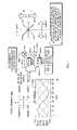
- FIG. 1is a block diagram of a signal converter according to the invention.
- FIG. 2is a more detailed diagram of the modulation chain in an optical to electrical or transmitter portion.
- FIG. 3is a logic circuit diagram for a serial to parallel converter in the modulation chain.
- FIG. 4is a true table for a Differential Quadrature Phase Shift Keying (DQPSK) encoder.
- DQPSKDifferential Quadrature Phase Shift Keying
- FIG. 5illustrates QPSK modulation
- FIG. 6is a more detailed diagram of the demodulation chain in the electrical to optical or receiver position.
- FIG. 7illustrates the operation of a DQPSK demodulator.
- FIG. 8is a more detailed diagram of a typical embodiment of the clock and data recovery circuit.
- FIG. 9is a block diagram showing alternate embodiments of the radio frequency portion of the transmitter and receiver.
- FIG. 10is a block diagram illustrating an optical telemetry interface.
- FIG. 1is a block diagram of an optical to wireless microwave signal converter 10 according to the invention.
- the converter 10includes an optical to electrical or microwave transmitter portion 100 and an electrical to optical or microwave receiver portion 200 . It should be understood that in a typical point to point system, there will be two converters 10 , each associated with one of two end points of a communication link.
- the microwave transmitter portion 100uses an optical transceiver 102 to receive an input optical signal.
- the optical signalis a high data rate protocol encoded signal such as a SONET signal. It should be understood that other types of optical transport signals such as Gigabit Ethernet (GE) signals may be converted to microwave signals using the principles of the present invention.
- the optical transceiverconverts the optical signal to an electric signal, which in turn is fed to a Clock and Data Recovery (CDR) circuit 104 .
- the CDR 104provides a Data signal and a Clock signal to a differential encoder 106 .
- the differential encoder 106which will be described in greater detail in connection with FIG. 2 , provides a pair of output signals to a respective pair of low pass filters 108 - 1 and 108 - 2 . It suffices here to say that the differential encoder 106 encodes the signal on a symbol by symbol basis, two bits at a time. The information is preferably encoded differentially for input to a Quadrature Phase Shift Keying (QPSK) modulator. This type of encoding requires the differential encoder 106 to retain knowledge of the last output signal as well as having access to the present input signal. The resulting in-phase (I) and quadrature (Q) bit streams provided to the filters 108 - 1 and 108 - 2 thus represent an encoded phase change. The output of the encoder is a pair of parallel bit streams at one-half the input data rate
- a QPSK modulator 110uses the I and Q bit streams to modulate a local oscillator.
- the modulator 110thus consists of a local oscillator 111 , a 90-degree hybrid 114 , and output mixers 112 - 1 and 112 - 2 .
- the QPSK modulator 110takes the encoded I and Q signals from filters 108 , up-converts them to a quadrature modulated output signal at the output of combiner 118 .
- the QPSK modulatorprovides an output signal at an Intermediate Frequency (IF) such as 3.3 GHz.
- IFIntermediate Frequency
- the resulting quadrature modulated signalis fed to a microwave frequency RF chain consisting of a partial raised cosine bandpass filter 126 , an up-converter oscillator, and mixer chain, including local microwave oscillator 125 , frequency multiplier 127 , and up-converter mixer 128 .
- the output of up-converter mixer 128is a signal in the 60 GHz or V-band range. This signal feeds a final LO and image reject filter 130 and output power amplifier 132 .
- the transmit signalis then fed through the transmit portion of a waveguide diplexer 150 to an antenna port 175 .
- a microwave receiver portion 200operates on microwave signals received at the antenna port 175 .
- a receive portion of the diplexer 150feeds a low noise amplifier 210 .
- An image reject filter 212removes undesirable sidebands feeding a down-converter mixer chain including a local oscillator 214 , multiplier 218 , and down-converter mixer 220 .
- a receiver amplifier 224feeds a partial raised cosine filter 230 . This provides a signal at approximately a 6 GHz frequency to a non-coherent DQPSK demodulator 240 .
- the DQSPK demodulator 240(discussed in greater detail below) consists of a pair of delay units 242 - 1 and 242 - 2 that provide a minus 45° and plus 45° delay, respectively.
- the received signalsare then demodulated with the mixers 244 - 1 and 244 - 2 , respectively, to provide an in phase (I) and quadrature (Q) representation. Passing through respective low pass filters 246 - 1 and 246 - 2 , the I and Q signals are then fed to a pair of CDR circuits 250 - 1 and 250 - 2 .
- These CDR circuitsoperating at one half of the original digital bit stream rate, provide resulting I and Q data streams to a parallel to serial converter 256 .
- a selected one of the CDRs 250 - 1 or 250 - 2is then used as a clock reference to drive the parallel to serial converter 256 .
- the resulting output of the differential decoder 260is then fed to a final CDR circuit 270 to further re-time the digital bit stream prior to being fed to the transmit portion of the optical transceiver 102 .
- the delay elements 242 - 1 and 242 - 2may be provided by a transmission line with a length set to delay the signal by one symbol period.
- the input signalis a Gigabit Ethernet (GigE) type signal and the bit rate is 1.25 Gigabits per second (Gbps)
- the transmitted symbol rate output by the differential encoderis 0.625 Gbps, and the symbol period is therefore 1.6 nanoseconds (ns).
- the bit rateis 0.622 Gbps
- the transmitted symbol rateis 0.311 Gbps and the symbol period is 3.215 ns.
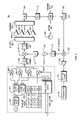
- FIG. 2shows the modulation chain in more detail.
- the differential encoder 106is seen to include a serial to parallel logic circuit 138 , a differential encoder circuit 140 , and a divide-by-two clock circuit 139 .
- the divide by two clock circuit 139provides a clock reference for the serial to parallel logic, that provides two output streams 107 - 1 and 107 - 2 by de-interleaving the input serial bit stream from the optical transceiver For example, in a Gigabit Ethernet application where input data stream is at 1.25 Gigabits per second (Gbps), the resulting two bit streams are at 0.625 Gbps.
- the serial-to-parallel logic 138is shown in FIG. 3 ; it consists of three D-type flip-flops, 1380 - 1 , 1380 - 2 , and 1380 - 3 .
- the flip-flop 1380 - 2clocks out every odd numbered incoming bit at one-half the bit rate.
- the flip-flop 1380 - 3clocks out every even numbered incoming bit at half the bit rate.
- the resulting two I and Q bit streamsarrive at the modulator 110 at the same time representing a data symbol as a two-bit pair.
- a logic table diagram 1400 for the 2-bit differential encoderis shown in FIG. 4 .
- This logic table 1400is for a differential type encoder that requires both a current input symbol and last output symbol in order to determine a current output symbol.
- Current output bits ⁇ 1 , and ⁇ iare shown on the right hand side of the chart. These respectively provide the in-phase (I) and quadrature (Q) outputs of the encoder 106 .
- the output symbol assignmentis thus shown in the phase diagram 1420 where an output symbol pair of (1,1) is translated by the modulator to a phase shift of 45°, a symbol pair of (0,1) is an output phase shift of +135°, a symbol pair of (0,0) is a phase of ⁇ 135°, and a symbol pair of (1,0) is a phase of ⁇ 45°.
- thispermits the quadrature modulator 110 to provide the desired output for distinct phases representing two-bit combinations as shown.
- FIG. 6shows a more detailed view of the non-coherent DQPSK demodulator 240 and associated parallel to serial logic 260 .
- the input signalfor example, at an IF of 5.625 GHz, is split by power divider 241 - 1 to two paths through a further pair of splitters 241 - 2 and 241 - 3 . These outputs are fed to drive mixer pairs 244 - 1 and 244 - 2 .
- the other input to the mixer pairare the quadrature signals derived from the delay line 245 - 1 and hybrid circuit 243 - 1 .
- the resulting outputs from the amplifiers 249 - 1 and 249 - 2are an I and Q signal pair, at a half the desired data rate, having been down-converted from the 5.625 GHz IF.
- the pair of CDR circuits 250 - 1 and 250 - 2then operate on each of the respective I and Q signal paths. These circuits recover the bit clock from I 251 - 1 and Q 252 - 1 signals in cleaner digital form.
- the parallel to serial logic 256combines the two baseband bit streams back to a single bit stream 254 prior to its being fed to the final CDR circuit 270 . At this point, the original bit stream at the full data rate is recovered.
- This final CDR circuit 270provides for further synchronization of the output bit stream before being fed to the optical transceiver 102 .
- FIG. 7is a more detailed view of the operation of the DQPSK demodulator 240 .
- the incoming signalis fed to the signal splitters and delays 242 and mixers 244 - 1 and 244 - 2 to provide in-phase and quadrature signals.
- the input symbol assignmentshown in the phasor diagram 2410 , corresponds to the transmit symbol assignment as previously described. Because each phase detector must resolve both 1 and 0 in I and Q independently, it is not possible to use phase differences of 0, +90, ⁇ 90 and 180 because phase differences of +90 and ⁇ 90 produce the same result in certain bit sequence combinations. However, by rotating the Cartesian plane by 45 degrees, zeros and ones in the I and Q can be determined without ambiguity. It is therefore, in a preferred embodiment, necessary to have the symbol assignments as shown, with the phasor values set for ⁇ 45° and ⁇ 135°.
- FIG. 8is a detailed view of a typical embodiment of the clock and data recovery circuit 104 used on the transmit side as well as circuits 250 - 1 , 250 - 2 and 270 used on the receiver side.
- the CDR circuitmay be the model SY87701L available from Micrel Corporation.
- This chipis a clock and data recovery integrated circuit that operates with data rates from 32 megabits per second up to 1.25 gigabits per second. Clock and data timing recovery is performed by synchronizing an on-chip, Voltage Controlled Oscillator (VCO) 810 directly to an incoming data stream 820 , through the use of a phase lock loop 808 .
- VCOVoltage Controlled Oscillator
- Flip-flop 812 and drivers 814 - 1 and 814 - 2provide the retimed data and recovered clock outputs.
- the pair of timing recovery circuits 250reduces the need for precise timing relative to the transmitter. This also provides a number of advantages. In particular, since the clock and data recovery circuits 250 are relatively inexpensive, two CDR circuits can be used, with each one operating at one-half the data rate.
- the conversion circuit 10may process optical signals of different types regardless of how they are coded.
- the microwave radio signalis modulated without need for knowledge of the baseband formatting of the incoming optical signal or the protocol used to encode that data stream.
- the resulting radio designis independent of the protocol used to encode the data at layers above the physical layer. Any bit rate signal within range of the clock and data recovery units can be processed, and properly up-converted by the transmit chain 100 and down-converted by the receive chain 200 .
- FIG. 9is a block diagram of certain portions of microwave transmitter 100 and receiver 200 illustrating alternate arrangements for various elements. These include (a) a common local oscillator for the transmitter 100 and receiver 200 ; (b) extending the microwave frequency range with an output multiplier and appropriate adjustment to the phase shifter; (c) an Ortho-Mode Transducer (OMT) or circulator in conjunction with filters in place of the frequency diplexer; and/or (d) multiple MMIC power amplifiers. It should be understood that each of these approaches may be used independently or in combination with one another as design alternatives.
- OMTOrtho-Mode Transducer
- a single local oscillator 901is operating in the range of from 10 to 15 GHz.
- the IF frequency provided by the output of the modulator and at the input to the demodulator 260would be the same.
- the single local oscillator 901thus can serve both the transmitter portion 100 and receiver portion 200 .
- the output frequency range for the microwave carrier signalscan also be extended through the use of a final stage frequency multiplier 940 .
- the multiplier 940is a times L frequency multiplier, where L is an integer such as 2 or 4.
- the frequency multiplier 940is inserted in the output RF chain such as before the final filter 950 .
- the multiplier 940allows for use of higher range microwave carrier frequencies than might otherwise be possible.
- the phase statesare adjusted depending upon the multiplication factor, L.
- the modulator 110generates four phase states using phase splitters 951 , 952 , 953 and summers 955 - 1 , 955 - 2 , 955 - 3 , 955 - 4 , as shown.
- the proper phase45, ⁇ 45, 135, or ⁇ 135
- the proper phase(0, 90, 180, or ⁇ 90) from the sum of the lower two mixers 955 - 3 , 955 - 4
- the logic tableshows the mapping from data to the inputs to the four mixers used as 180 degree phase shifters.
- the output frequency rangemay be such that a low noise amplifier 210 used in the embodiment of FIG. 1 is not needed. Specifically, because of the higher microwave frequencies involved, it may not be possible to use amplifiers that have acceptable noise performance. In this instance, a harmonic mixer 220 might be used in the receiver 200 to recover the microwave signal of interest. In the case where the frequency multiplier 940 factor, L, is two, the harmonic mixer 220 should be a second harmonic mixer.
- Additional embodimentsmay include the introduction of multiple amplifiers 920 in the output transmit stage to boost the total output power.
- the amplifiers 920are fed by appropriate splitter 910 (or network of splitters) and combined at their outputs by an appropriate combiner 930 and/or combiner network.
- the diplexer 150 of the FIG. 1 embodimentmight be replaced by either an Ortho-Mode Transducer (OMT) 955 or a circulator 956 . Since neither an OMT 955 nor a circulator 956 provides filtering it is necessary to include a transmit final filter 950 and receive initial filter 960 .
- OMTOrtho-Mode Transducer
- the inventioncan also provide a low speed telemetry interface for a point-to-point optical to microwave converter 10 using optical cables.
- FIG. 10shows additional embellishments of the invention that might be used to provide a low data rate telemetry interface. Shown is a high level diagram of the radio related components that are associated with optical to microwave conversion of a high speed data signal.
- theseinclude the optical transceiver 102 , encoder 106 , modulator 110 and up converter 102 a (which includes for example the filter 126 , mixer 128 , oscillator 125 , multiplier 127 , filter 130 and amplifier 132 as well as down converter 1020 , which include amplifiers 210 , 224 , filters 212 , 230 , mixer 220 , multiplier 218 and oscillator 214 of FIG. 1 ), demodulator 240 and decoder 260 .
- up converter 102 awhich includes for example the filter 126 , mixer 128 , oscillator 125 , multiplier 127 , filter 130 and amplifier 132 as well as down converter 1020 , which include amplifiers 210 , 224 , filters 212 , 230 , mixer 220 , multiplier 218 and oscillator 214 of FIG. 1 .
- One or more of the components of the converter 10might provide alarm, status, or other signals relating to their operation and maintenance, or may accept configuration or programming signals. Such signals are provided to or from a microcontroller 1100 that is formed as part of the converter 10 .
- the converter 10is typically located in an outdoor location that is remote from the data terminal equipment 1500 that provides the source optical (OC-12 or GigE type) signals that carry the high speed data 1250 .
- a telemetry interface 1200that permits a host computer 1550 associated with terminal equipment 1500 to control the converter 10 . It is advantageous to provide this telemetry interface 1200 as a fiber optic low data rate interface. This avoids ground differential and over-voltage protection issues that might be associated with the typical copper wire (e.g, coaxial cable) interface.
- the remote located converter(or access unit 1000 ) includes an optical telemetry interface 1200 that uses a separate multimode fiber pair 1200 as a communications medium.
- the interface 1200may carry asynchronous serial data, for example, to and from the access unit 1000 at a data rate of 57,600 bits per second in the common serial format of 8 data bits with no parity and one stop bit, such as using standard RS-232 signaling.
- the telemetry signalingtypically includes remote control and monitoring of the access unit 1000 as well as the ability to perform upgrades of for example, firmware stored within an electrically erasable memory 1111 associated with the microcontroller 1100 .
- Fiber optic cables 1200are chosen as a preferred transport medium for telemetry signals because they provide several key advantages that ultimately contribute to a more reliable unit 1000 . These include elimination of electrostatic discharge, electromagnetic interference, effects radio frequency interference and similar susceptibility issues that would be inherent in the event a copper type RS-232 interface were used. In addition, ground loops that might be common with copper differential pair RS-422/RS-485 type interfaces are also avoided. The risk of lightning damage to 1100 also is reduced.
- An optical telemetry interface 1250provides for a minimum parts count, and longer communication distances without the need to provide signal termination circuits.
- the access unit 1000would include a hardware Universal Asynchronous Receiver/Transmitter (UART) 1115 which might be integral with the micro controller 1100 .
- UARTUniversal Asynchronous Receiver/Transmitter
- the UARTprovides the electrical functions for transmitting and receiving the telemetry signals. Since the UART operates with typically a five volt Transistor Transistor Logic (TTL) interface 1118 , conversion to and from the optical is made with fiber optic transmitter 1130 and receiver 1120 .
- TTLTransistor Transistor Logic
- the fiber optic transmitter 1130which might be implemented with LED transmitter technology, transmits the TTL signal to an optical signal; the fiber optic receiver 1120 similarly transmits a received optical signal to a TTL signal.
- the fiber optic telemetry interfaceuses a commercial off-the-shelf RS-232 fiber optic modem 1520 .
- Fiber optic modem 1520can provide the translation of RS-232 electrical signals from the incoming low-speed telemetry received as optical signals and also converting electrical signals for transmission to optical form.
- the telemetry messagesare encoded using a 16 bit Cyclic Redundancy Check (CRC) to insure a high level of data integrity.
- Layered communication protocolsmay be used, as is well known in the art. For example, Simple Network Management Protocol (SNMP) messaging can be layered over the RS-232. Other sorts of protocols can be provided for.
- 10baseT type signalingis used instead of RS-232 for the low data rate interface 1200 .
- Internet Protocol (IP) type signalingcould be used to carry the telemetry, with the access unit 100 having a dedicated IP address for this purpose.
- IPInternet Protocol
Landscapes
- Physics & Mathematics (AREA)
- Electromagnetism (AREA)
- Engineering & Computer Science (AREA)
- Computer Networks & Wireless Communication (AREA)
- Signal Processing (AREA)
- Digital Transmission Methods That Use Modulated Carrier Waves (AREA)
Abstract
Description
Claims (28)
Priority Applications (1)
| Application Number | Priority Date | Filing Date | Title |
|---|---|---|---|
| US10/196,568US7103279B1 (en) | 2002-07-15 | 2002-07-15 | Architecture for wireless transmission of high rate optical signals |
Applications Claiming Priority (1)
| Application Number | Priority Date | Filing Date | Title |
|---|---|---|---|
| US10/196,568US7103279B1 (en) | 2002-07-15 | 2002-07-15 | Architecture for wireless transmission of high rate optical signals |
Publications (1)
| Publication Number | Publication Date |
|---|---|
| US7103279B1true US7103279B1 (en) | 2006-09-05 |
Family
ID=36939559
Family Applications (1)
| Application Number | Title | Priority Date | Filing Date |
|---|---|---|---|
| US10/196,568Expired - Fee RelatedUS7103279B1 (en) | 2002-07-15 | 2002-07-15 | Architecture for wireless transmission of high rate optical signals |
Country Status (1)
| Country | Link |
|---|---|
| US (1) | US7103279B1 (en) |
Cited By (36)
| Publication number | Priority date | Publication date | Assignee | Title |
|---|---|---|---|---|
| US20050259992A1 (en)* | 2004-05-19 | 2005-11-24 | Alcatel | Method of operating an optical transmission system with a bit-to-bit polarization interleaved bitstream |
| US20070147278A1 (en)* | 2002-05-31 | 2007-06-28 | Adc Wireless Solutions Llc | System and method for retransmission of data |
| US20080141097A1 (en)* | 2003-08-21 | 2008-06-12 | Qualcomm Incorporated | Outer coding methods for broadcast/multicast content and related apparatus |
| US20080267314A1 (en)* | 2005-12-30 | 2008-10-30 | Idan Bar-Sade | Digital microwave radio system and method with encryption |
| US20100034316A1 (en)* | 2007-08-07 | 2010-02-11 | Trex Enterprises Corp. | Millimeter wave radio with phase modulation |
| US20100062707A1 (en)* | 2008-09-05 | 2010-03-11 | Huawei Technologies Co., Ltd. | Frequency conversion device, method and system |
| US20100150565A1 (en)* | 2008-12-17 | 2010-06-17 | Huawei Technologies Co., Ltd. | Method and apparatus for transmitting/receiving signals in a microwave system |
| US7817958B2 (en) | 2006-12-22 | 2010-10-19 | Lgc Wireless Inc. | System for and method of providing remote coverage area for wireless communications |
| CN101894090A (en)* | 2010-06-13 | 2010-11-24 | 昆山五昌新精密电子工业有限公司 | RS-485 signal converter capable of automatically adjusting transmitting-receiving order |
| US7844273B2 (en) | 2006-07-14 | 2010-11-30 | Lgc Wireless, Inc. | System for and method of for providing dedicated capacity in a cellular network |
| US7848770B2 (en) | 2006-08-29 | 2010-12-07 | Lgc Wireless, Inc. | Distributed antenna communications system and methods of implementing thereof |
| US20110020012A1 (en)* | 2009-06-19 | 2011-01-27 | Hitachi, Ltd. | Optical signal receiving apparatus |
| US20110081872A1 (en)* | 2005-12-30 | 2011-04-07 | Bridgewave Communications, Inc. | Digital Microwave Radio Link with a Variety of Ports |
| US20110122932A1 (en)* | 2008-08-07 | 2011-05-26 | Trex Enterprises Corp. | High data rate milllimeter wave radio on a chip |
| US7962111B2 (en) | 2002-02-25 | 2011-06-14 | ADC Wireless, Inc. | Distributed automatic gain control system |
| US8005050B2 (en) | 2007-03-23 | 2011-08-23 | Lgc Wireless, Inc. | Localization of a mobile device in distributed antenna communications system |
| US8010116B2 (en) | 2007-06-26 | 2011-08-30 | Lgc Wireless, Inc. | Distributed antenna communications system |
| WO2012074551A1 (en)* | 2010-11-30 | 2012-06-07 | Trex Enterprises Corporation | High data rate millimeter wave radio |
| US8385461B1 (en)* | 2009-04-20 | 2013-02-26 | Vubiq, Inc. | On-off keying using vector modulation |
| US8451770B2 (en) | 2002-05-06 | 2013-05-28 | Qualcomm Incorporated | Multi-media broadcast and multicast service (MBMS) in a wireless communication system |
| US8694869B2 (en) | 2003-08-21 | 2014-04-08 | QUALCIMM Incorporated | Methods for forward error correction coding above a radio link control layer and related apparatus |
| US8711888B2 (en) | 2005-12-30 | 2014-04-29 | Remec Broadband Wireless Llc | Digital microwave radio link with adaptive data rate |
| US8804761B2 (en)* | 2003-08-21 | 2014-08-12 | Qualcomm Incorporated | Methods for seamless delivery of broadcast and multicast content across cell borders and/or between different transmission schemes and related apparatus |
| US8958513B1 (en)* | 2013-03-15 | 2015-02-17 | Xilinx, Inc. | Clock and data recovery with infinite pull-in range |
| US9001811B2 (en) | 2009-05-19 | 2015-04-07 | Adc Telecommunications, Inc. | Method of inserting CDMA beacon pilots in output of distributed remote antenna nodes |
| US9112547B2 (en) | 2007-08-31 | 2015-08-18 | Adc Telecommunications, Inc. | System for and method of configuring distributed antenna communications system |
| US20160204823A1 (en)* | 2008-08-07 | 2016-07-14 | Trex Enterprises Corporation | 10GbE E-band radio with 8PSK modulation |
| US9577922B2 (en) | 2014-02-18 | 2017-02-21 | Commscope Technologies Llc | Selectively combining uplink signals in distributed antenna systems |
| US10498434B2 (en) | 2000-07-19 | 2019-12-03 | CommScope Technolgies LLC | Point-to-multipoint digital radio frequency transport |
| US10499269B2 (en) | 2015-11-12 | 2019-12-03 | Commscope Technologies Llc | Systems and methods for assigning controlled nodes to channel interfaces of a controller |
| US10778277B1 (en)* | 2019-04-21 | 2020-09-15 | Siklu Communication ltd. | Methods and systems for utilizing millimeter-wave radio components in synthesizing microwave signals |
| CN114295013A (en)* | 2021-12-28 | 2022-04-08 | 江南机电设计研究所 | Binding method for remote measuring frequency points |
| US11431432B2 (en)* | 2003-06-10 | 2022-08-30 | Alexander Soto | System and method for performing high-speed communications over fiber optical networks |
| US11522613B2 (en)* | 2019-04-29 | 2022-12-06 | Hangzhou Xin Yun Technology Co., Ltd | Adjustable bidirectional transmission micro-optoelectronic system supporting online upgrade configuration |
| USRE49377E1 (en) | 2002-12-03 | 2023-01-17 | Commscope Technologies Llc | Distributed digital antenna system |
| EP4152645A1 (en)* | 2021-09-21 | 2023-03-22 | Apple Inc. | Communication devices and methods for direct detection and photonics receiver |
Citations (1)
| Publication number | Priority date | Publication date | Assignee | Title |
|---|---|---|---|---|
| US6480477B1 (en)* | 1997-10-14 | 2002-11-12 | Innowave Eci Wireless Systems Ltd. | Method and apparatus for a data transmission rate of multiples of 100 MBPS in a terminal for a wireless metropolitan area network |
- 2002
- 2002-07-15USUS10/196,568patent/US7103279B1/ennot_activeExpired - Fee Related
Patent Citations (1)
| Publication number | Priority date | Publication date | Assignee | Title |
|---|---|---|---|---|
| US6480477B1 (en)* | 1997-10-14 | 2002-11-12 | Innowave Eci Wireless Systems Ltd. | Method and apparatus for a data transmission rate of multiples of 100 MBPS in a terminal for a wireless metropolitan area network |
Non-Patent Citations (4)
| Title |
|---|
| GigaLink Product Specification. |
| Loea Communications Corporation, Loea Communications Corporation Solving the "Last Mile Problem" with the "Last 10 Miles Solution" (2001). |
| Noreus, J., et al., "System Considerations for Hardware Parameters in a 60 GHz WLAN". |
| SierraCom, "SierraCom's FiberConnection(TM) Series 60 Ghz Radio for US Markets," ISO-9001 Certified Facility. |
Cited By (61)
| Publication number | Priority date | Publication date | Assignee | Title |
|---|---|---|---|---|
| US10498434B2 (en) | 2000-07-19 | 2019-12-03 | CommScope Technolgies LLC | Point-to-multipoint digital radio frequency transport |
| US10505635B2 (en) | 2000-07-19 | 2019-12-10 | Commscope Technologies Llc | Point-to-multipoint digital radio frequency transport |
| US7962111B2 (en) | 2002-02-25 | 2011-06-14 | ADC Wireless, Inc. | Distributed automatic gain control system |
| US8451770B2 (en) | 2002-05-06 | 2013-05-28 | Qualcomm Incorporated | Multi-media broadcast and multicast service (MBMS) in a wireless communication system |
| US7702985B2 (en)* | 2002-05-31 | 2010-04-20 | Adc Wireless Solutions Llc | System and method for retransmission of data |
| US20070147278A1 (en)* | 2002-05-31 | 2007-06-28 | Adc Wireless Solutions Llc | System and method for retransmission of data |
| USRE49377E1 (en) | 2002-12-03 | 2023-01-17 | Commscope Technologies Llc | Distributed digital antenna system |
| USRE50112E1 (en) | 2002-12-03 | 2024-09-03 | Outdoor Wireless Networks LLC | Distributed digital antenna system |
| US11431432B2 (en)* | 2003-06-10 | 2022-08-30 | Alexander Soto | System and method for performing high-speed communications over fiber optical networks |
| US11641247B2 (en) | 2003-06-10 | 2023-05-02 | Alexander Soto | System and method for performing high-speed communications over fiber optical networks |
| US8171381B2 (en) | 2003-08-21 | 2012-05-01 | Qualcomm Incorporated | Outer coding methods for broadcast/multicast content and related apparatus |
| US8694869B2 (en) | 2003-08-21 | 2014-04-08 | QUALCIMM Incorporated | Methods for forward error correction coding above a radio link control layer and related apparatus |
| US20080141097A1 (en)* | 2003-08-21 | 2008-06-12 | Qualcomm Incorporated | Outer coding methods for broadcast/multicast content and related apparatus |
| US8804761B2 (en)* | 2003-08-21 | 2014-08-12 | Qualcomm Incorporated | Methods for seamless delivery of broadcast and multicast content across cell borders and/or between different transmission schemes and related apparatus |
| US8291300B2 (en) | 2003-08-21 | 2012-10-16 | Qualcomm Incorporated | Outer coding methods for broadcast/multicast content and related apparatus |
| US20080141094A1 (en)* | 2003-08-21 | 2008-06-12 | Qualcomm Incorporated | Outer coding methods for broadcast/multicast content and related apparatus |
| US8175090B2 (en) | 2003-08-21 | 2012-05-08 | Qualcomm Incorporated | Outer coding methods for broadcast/multicast content and related apparatus |
| US20050259992A1 (en)* | 2004-05-19 | 2005-11-24 | Alcatel | Method of operating an optical transmission system with a bit-to-bit polarization interleaved bitstream |
| US7616898B2 (en)* | 2004-05-19 | 2009-11-10 | Alcatel | Method of operating an optical transmission system with a bit-to-bit polarization interleaved bitstream |
| US20110081872A1 (en)* | 2005-12-30 | 2011-04-07 | Bridgewave Communications, Inc. | Digital Microwave Radio Link with a Variety of Ports |
| US8711888B2 (en) | 2005-12-30 | 2014-04-29 | Remec Broadband Wireless Llc | Digital microwave radio link with adaptive data rate |
| US8731007B2 (en)* | 2005-12-30 | 2014-05-20 | Remec Broadband Wireless, Llc | Digital microwave radio link with a variety of ports |
| US20080267314A1 (en)* | 2005-12-30 | 2008-10-30 | Idan Bar-Sade | Digital microwave radio system and method with encryption |
| US9059866B2 (en) | 2005-12-30 | 2015-06-16 | Remec Broadband Wireless Holdings, Inc. | Digital microwave radio system and method with encryption |
| US7844273B2 (en) | 2006-07-14 | 2010-11-30 | Lgc Wireless, Inc. | System for and method of for providing dedicated capacity in a cellular network |
| US7848770B2 (en) | 2006-08-29 | 2010-12-07 | Lgc Wireless, Inc. | Distributed antenna communications system and methods of implementing thereof |
| US7817958B2 (en) | 2006-12-22 | 2010-10-19 | Lgc Wireless Inc. | System for and method of providing remote coverage area for wireless communications |
| USRE45505E1 (en) | 2007-03-23 | 2015-05-05 | Adc Telecommunications, Inc. | Localization of a mobile device in distributed antenna communications system |
| US8005050B2 (en) | 2007-03-23 | 2011-08-23 | Lgc Wireless, Inc. | Localization of a mobile device in distributed antenna communications system |
| US8229497B2 (en) | 2007-06-26 | 2012-07-24 | Lgc Wireless, Llc | Distributed antenna communications system |
| US8010116B2 (en) | 2007-06-26 | 2011-08-30 | Lgc Wireless, Inc. | Distributed antenna communications system |
| US8532698B2 (en) | 2007-06-26 | 2013-09-10 | Adc Telecommunications, Inc. | Distributed antenna communications system |
| US20100034316A1 (en)* | 2007-08-07 | 2010-02-11 | Trex Enterprises Corp. | Millimeter wave radio with phase modulation |
| US8098764B2 (en)* | 2007-08-07 | 2012-01-17 | Trex Enterprises Corp. | Millimeter wave radio with phase modulation |
| US9112547B2 (en) | 2007-08-31 | 2015-08-18 | Adc Telecommunications, Inc. | System for and method of configuring distributed antenna communications system |
| US20110122932A1 (en)* | 2008-08-07 | 2011-05-26 | Trex Enterprises Corp. | High data rate milllimeter wave radio on a chip |
| US9300508B2 (en)* | 2008-08-07 | 2016-03-29 | Trex Enterprises Corp. | High data rate milllimeter wave radio on a chip |
| US20160204823A1 (en)* | 2008-08-07 | 2016-07-14 | Trex Enterprises Corporation | 10GbE E-band radio with 8PSK modulation |
| US20100062707A1 (en)* | 2008-09-05 | 2010-03-11 | Huawei Technologies Co., Ltd. | Frequency conversion device, method and system |
| US8385745B2 (en)* | 2008-12-17 | 2013-02-26 | Huawei Technologies Co., Ltd. | Method and apparatus for transmitting/receiving signals in a microwave system |
| US20100150565A1 (en)* | 2008-12-17 | 2010-06-17 | Huawei Technologies Co., Ltd. | Method and apparatus for transmitting/receiving signals in a microwave system |
| US8385461B1 (en)* | 2009-04-20 | 2013-02-26 | Vubiq, Inc. | On-off keying using vector modulation |
| US9001811B2 (en) | 2009-05-19 | 2015-04-07 | Adc Telecommunications, Inc. | Method of inserting CDMA beacon pilots in output of distributed remote antenna nodes |
| US20110020012A1 (en)* | 2009-06-19 | 2011-01-27 | Hitachi, Ltd. | Optical signal receiving apparatus |
| US8340532B2 (en)* | 2009-06-19 | 2012-12-25 | Hitachi, Ltd. | Optical signal receiving apparatus |
| WO2011084839A1 (en)* | 2010-01-08 | 2011-07-14 | Bridgewave Communicati0Ns, Inc. | Improved digital microwave radio link with a variety of ports |
| EP2522157A4 (en)* | 2010-01-08 | 2013-11-20 | Bridgewave Communications Inc | Improved digital microwave radio link with a variety of ports |
| CN101894090B (en)* | 2010-06-13 | 2012-05-23 | 昆山五昌新精密电子工业有限公司 | RS-485 signal converter capable of automatically adjusting transmitting-receiving order |
| CN101894090A (en)* | 2010-06-13 | 2010-11-24 | 昆山五昌新精密电子工业有限公司 | RS-485 signal converter capable of automatically adjusting transmitting-receiving order |
| WO2012074551A1 (en)* | 2010-11-30 | 2012-06-07 | Trex Enterprises Corporation | High data rate millimeter wave radio |
| US8958513B1 (en)* | 2013-03-15 | 2015-02-17 | Xilinx, Inc. | Clock and data recovery with infinite pull-in range |
| US10291295B2 (en) | 2014-02-18 | 2019-05-14 | Commscope Technologies Llc | Selectively combining uplink signals in distributed antenna systems |
| US9577922B2 (en) | 2014-02-18 | 2017-02-21 | Commscope Technologies Llc | Selectively combining uplink signals in distributed antenna systems |
| US10499269B2 (en) | 2015-11-12 | 2019-12-03 | Commscope Technologies Llc | Systems and methods for assigning controlled nodes to channel interfaces of a controller |
| US10778277B1 (en)* | 2019-04-21 | 2020-09-15 | Siklu Communication ltd. | Methods and systems for utilizing millimeter-wave radio components in synthesizing microwave signals |
| US11522613B2 (en)* | 2019-04-29 | 2022-12-06 | Hangzhou Xin Yun Technology Co., Ltd | Adjustable bidirectional transmission micro-optoelectronic system supporting online upgrade configuration |
| EP4152645A1 (en)* | 2021-09-21 | 2023-03-22 | Apple Inc. | Communication devices and methods for direct detection and photonics receiver |
| US20230090151A1 (en)* | 2021-09-21 | 2023-03-23 | Apple Inc. | Communication devices and methods for direct detection and photonics receiver |
| US11848703B2 (en)* | 2021-09-21 | 2023-12-19 | Apple Inc. | Communication devices and methods for direct detection and photonics receiver |
| CN114295013B (en)* | 2021-12-28 | 2024-03-29 | 江南机电设计研究所 | Telemetering frequency point binding method |
| CN114295013A (en)* | 2021-12-28 | 2022-04-08 | 江南机电设计研究所 | Binding method for remote measuring frequency points |
Similar Documents
| Publication | Publication Date | Title |
|---|---|---|
| US7103279B1 (en) | Architecture for wireless transmission of high rate optical signals | |
| US9300508B2 (en) | High data rate milllimeter wave radio on a chip | |
| EP2044784B1 (en) | Antenna array system | |
| EP2044686B1 (en) | Digital transceiver | |
| US20050260952A1 (en) | Bridged ultra-wideband communication method and apparatus | |
| US9008212B2 (en) | High data rate millimeter wave radio | |
| US6185201B1 (en) | Multiplex radio transmitter and multiplex radio transmission method, multiplex radio receiver and multiplex radio receiving method, and multiplex radio transceiver and multiplex transmission/receiving system | |
| US8811558B2 (en) | Method of synchronizing two electronic devices of a wireless link, in particular of a mobile telephone network and system for implementing this method | |
| US20040166817A1 (en) | System, method and apparatus for burst communications | |
| WO2001097420A2 (en) | Multiplexing digital communication system | |
| US6301310B1 (en) | Efficient implementation for systems using CEOQPSK | |
| US4821261A (en) | Packet transmission of digital signals over a high capacity channel, particularly over a satellite broadcasting channel | |
| US6628605B1 (en) | Method and apparatus for efficiently transmitting multiple data signals | |
| US10122520B2 (en) | Microwave backhaul system having quadruple capacity | |
| US7702030B2 (en) | Module to module signaling with jitter modulation | |
| AU627012B2 (en) | Optical transmission system | |
| Chen et al. | A data-rate adaptable modem solution for millimeter-wave wireless fronthaul networks | |
| He et al. | A novel FPGA-based 2.5 Gbps D-QPSK modem for high capacity microwave radios | |
| US6496079B1 (en) | Optical to microwave converter using direct modulation phase shift keying | |
| US20040151237A1 (en) | Satellite communications system | |
| CN210958371U (en) | Inter-satellite laser ultra-wideband demodulation module | |
| US20040096010A1 (en) | Communications system including a narrow band modulator | |
| JP2877197B2 (en) | Non-regenerative relay alarm transmission apparatus and method | |
| CN117176255A (en) | An optical carrier simulation diverse radio frequency wireless transmission method for 5G fronthaul | |
| Entenman et al. | A supplier's response to IDR |
Legal Events
| Date | Code | Title | Description |
|---|---|---|---|
| AS | Assignment | Owner name:TELAXIS COMMUNICATIONS CORPORATION, MASSACHUSETTS Free format text:ASSIGNMENT OF ASSIGNORS INTEREST;ASSIGNORS:KOH, CHRISTOPHER T.;ROBINSON, WYLEY;LEE, MYUNG K.;AND OTHERS;REEL/FRAME:013593/0285 Effective date:20021121 | |
| AS | Assignment | Owner name:YDI WIRELESS, INC., MASSACHUSETTS Free format text:MERGER;ASSIGNOR:TELAXIS COMMUNICATIONS CORPORATION;REEL/FRAME:017741/0937 Effective date:20030707 | |
| AS | Assignment | Owner name:TERABEAM, INC., MASSACHUSETTS Free format text:MERGER;ASSIGNOR:YDI WIRELESS, INC.;REEL/FRAME:018253/0738 Effective date:20051103 | |
| FEPP | Fee payment procedure | Free format text:PAYOR NUMBER ASSIGNED (ORIGINAL EVENT CODE: ASPN); ENTITY STATUS OF PATENT OWNER: LARGE ENTITY | |
| AS | Assignment | Owner name:PROXIM WIRELESS CORPORATION, MASSACHUSETTS Free format text:MERGER;ASSIGNOR:TERABEAM, INC.;REEL/FRAME:020299/0907 Effective date:20070904 | |
| AS | Assignment | Owner name:TERABEAM CORPORATION, CALIFORNIA Free format text:ASSIGNMENT OF ASSIGNORS INTEREST;ASSIGNOR:PROXIM WIRELESS CORPORATION;REEL/FRAME:020762/0462 Effective date:20080403 | |
| AS | Assignment | Owner name:PERTEX TELECOMMUNICATION LLC, DELAWARE Free format text:ASSIGNMENT OF ASSIGNORS INTEREST;ASSIGNOR:TERABEAM CORPORATION;REEL/FRAME:021212/0859 Effective date:20080523 | |
| FEPP | Fee payment procedure | Free format text:PAYER NUMBER DE-ASSIGNED (ORIGINAL EVENT CODE: RMPN); ENTITY STATUS OF PATENT OWNER: LARGE ENTITY Free format text:PAYOR NUMBER ASSIGNED (ORIGINAL EVENT CODE: ASPN); ENTITY STATUS OF PATENT OWNER: LARGE ENTITY | |
| FPAY | Fee payment | Year of fee payment:4 | |
| FPAY | Fee payment | Year of fee payment:8 | |
| AS | Assignment | Owner name:OL SECURITY LIMITED LIABILITY COMPANY, DELAWARE Free format text:MERGER;ASSIGNOR:PERTEX TELECOMMUNICATION LLC;REEL/FRAME:037392/0187 Effective date:20150826 | |
| FEPP | Fee payment procedure | Free format text:MAINTENANCE FEE REMINDER MAILED (ORIGINAL EVENT CODE: REM.) | |
| LAPS | Lapse for failure to pay maintenance fees | Free format text:PATENT EXPIRED FOR FAILURE TO PAY MAINTENANCE FEES (ORIGINAL EVENT CODE: EXP.); ENTITY STATUS OF PATENT OWNER: LARGE ENTITY | |
| STCH | Information on status: patent discontinuation | Free format text:PATENT EXPIRED DUE TO NONPAYMENT OF MAINTENANCE FEES UNDER 37 CFR 1.362 | |
| FP | Lapsed due to failure to pay maintenance fee | Effective date:20180905 |