US7102943B2 - Non-volatile semiconductor memory device - Google Patents
Non-volatile semiconductor memory deviceDownload PDFInfo
- Publication number
- US7102943B2 US7102943B2US11/152,101US15210105AUS7102943B2US 7102943 B2US7102943 B2US 7102943B2US 15210105 AUS15210105 AUS 15210105AUS 7102943 B2US7102943 B2US 7102943B2
- Authority
- US
- United States
- Prior art keywords
- error
- write
- data
- memory
- correction circuit
- Prior art date
- Legal status (The legal status is an assumption and is not a legal conclusion. Google has not performed a legal analysis and makes no representation as to the accuracy of the status listed.)
- Expired - Fee Related
Links
Images


Classifications
- G—PHYSICS
- G11—INFORMATION STORAGE
- G11C—STATIC STORES
- G11C29/00—Checking stores for correct operation ; Subsequent repair; Testing stores during standby or offline operation
- G11C29/70—Masking faults in memories by using spares or by reconfiguring
- G11C29/76—Masking faults in memories by using spares or by reconfiguring using address translation or modifications
- G—PHYSICS
- G06—COMPUTING OR CALCULATING; COUNTING
- G06F—ELECTRIC DIGITAL DATA PROCESSING
- G06F11/00—Error detection; Error correction; Monitoring
- G06F11/07—Responding to the occurrence of a fault, e.g. fault tolerance
- G06F11/08—Error detection or correction by redundancy in data representation, e.g. by using checking codes
- G06F11/10—Adding special bits or symbols to the coded information, e.g. parity check, casting out 9's or 11's
- G06F11/1008—Adding special bits or symbols to the coded information, e.g. parity check, casting out 9's or 11's in individual solid state devices
- G06F11/1068—Adding special bits or symbols to the coded information, e.g. parity check, casting out 9's or 11's in individual solid state devices in sector programmable memories, e.g. flash disk
- G—PHYSICS
- G11—INFORMATION STORAGE
- G11C—STATIC STORES
- G11C16/00—Erasable programmable read-only memories
- G11C16/02—Erasable programmable read-only memories electrically programmable
- G11C16/06—Auxiliary circuits, e.g. for writing into memory
- G11C16/34—Determination of programming status, e.g. threshold voltage, overprogramming or underprogramming, retention
- G11C16/3418—Disturbance prevention or evaluation; Refreshing of disturbed memory data
- G11C16/3431—Circuits or methods to detect disturbed nonvolatile memory cells, e.g. which still read as programmed but with threshold less than the program verify threshold or read as erased but with threshold greater than the erase verify threshold, and to reverse the disturbance via a refreshing programming or erasing step
- G—PHYSICS
- G11—INFORMATION STORAGE
- G11C—STATIC STORES
- G11C29/00—Checking stores for correct operation ; Subsequent repair; Testing stores during standby or offline operation
- G11C29/70—Masking faults in memories by using spares or by reconfiguring
- G11C29/76—Masking faults in memories by using spares or by reconfiguring using address translation or modifications
- G11C29/765—Masking faults in memories by using spares or by reconfiguring using address translation or modifications in solid state disks
- G—PHYSICS
- G11—INFORMATION STORAGE
- G11C—STATIC STORES
- G11C29/00—Checking stores for correct operation ; Subsequent repair; Testing stores during standby or offline operation
- G11C29/70—Masking faults in memories by using spares or by reconfiguring
- G11C29/78—Masking faults in memories by using spares or by reconfiguring using programmable devices
- G11C29/80—Masking faults in memories by using spares or by reconfiguring using programmable devices with improved layout
- G11C29/81—Masking faults in memories by using spares or by reconfiguring using programmable devices with improved layout using a hierarchical redundancy scheme
- G—PHYSICS
- G11—INFORMATION STORAGE
- G11C—STATIC STORES
- G11C29/00—Checking stores for correct operation ; Subsequent repair; Testing stores during standby or offline operation
- G11C29/70—Masking faults in memories by using spares or by reconfiguring
- G11C29/78—Masking faults in memories by using spares or by reconfiguring using programmable devices
- G11C29/80—Masking faults in memories by using spares or by reconfiguring using programmable devices with improved layout
- G11C29/816—Masking faults in memories by using spares or by reconfiguring using programmable devices with improved layout for an application-specific layout
- G11C29/82—Masking faults in memories by using spares or by reconfiguring using programmable devices with improved layout for an application-specific layout for EEPROMs
- G—PHYSICS
- G11—INFORMATION STORAGE
- G11C—STATIC STORES
- G11C16/00—Erasable programmable read-only memories
- G11C16/02—Erasable programmable read-only memories electrically programmable
- G11C16/04—Erasable programmable read-only memories electrically programmable using variable threshold transistors, e.g. FAMOS
- G—PHYSICS
- G11—INFORMATION STORAGE
- G11C—STATIC STORES
- G11C29/00—Checking stores for correct operation ; Subsequent repair; Testing stores during standby or offline operation
- G11C29/04—Detection or location of defective memory elements, e.g. cell constructio details, timing of test signals
- G11C2029/0411—Online error correction
Definitions
- the present inventionrelates to a technology that may be applied to a non-volatile storage device, for example, to a technology that may be applied to a non-volatile semiconductor memory such as a flash memory or a card storage device such as a multimedia card or a smart media memory card.
- a non-volatile semiconductor memorysuch as a flash memory or a card storage device such as a multimedia card or a smart media memory card.
- a card storage devicecalled a memory card containing a non-volatile memory, such as a flash memory, that retains its storage data even after the power has been switched off, is widely used as a data storage medium for portable electronic apparatus such as a digital camera.
- a non-volatile memoryAs compared with a volatile memory such as a RAM, a non-volatile memory varies widely in its memory device characteristics. At the same time, a non-volatile memory is not designed basically for repeated write operation. Therefore, write errors occur relatively frequently in a memory card in which a non-volatile memory is contained. To solve the above problem, some memory cards containing non-volatile memories execute substitute processing to substitute another area for an area where an error has occurred.
- a flash memorywith a two-layer gate structure, stores data by taking advantage of a difference between the threshold voltage levels of the charge stored in the floating gate layer.
- injecting electrons into the floating gate layer to increase the threshold voltageis called a write, and the reverse operation is called an erasure.
- an excessive write errorsometimes occurs in which increasing the write voltage of a storage device in a flash memory sometimes changes the threshold voltage of a particular bit so greatly that the threshold gets out of a desired range.
- the write voltageshould be decreased.
- the problemis that a low write voltage prolongs the time required for writing. So, in general, with priority placed on a shorter write time rather than on a reduction in excessive write errors, the substitute processing described above is performed to recover excessive write error bits.
- some conventional memory cardscontain an error correction circuit to correct detected error bits before outputting them.
- a non-volatile-memory write erroroccurs in a card storage device containing a non-volatile memory and an error correction circuit
- write datais read from the non-volatile memory and a check is made if the error can be corrected by the error correction circuit. If the error can be corrected, the write operation is ended. If the error correction circuit cannot correct the error, substitute processing is performed to write data into some other area.
- substitute processingis performed to write data in some other area only when the error correction circuit cannot correct an error. Therefore, as compared with a method that always performs substitute processing when an error occurs, this method greatly reduces the number of substitution processing executions and, as a result, greatly reduces the data write time.
- the storage devicechecks if the error is a recoverable error such as an excessive write error which causes the threshold voltage to change greatly even under the same write operation condition.
- the storage devicechecks if the error correction circuit can correct the error only when the error is a recoverable error and, only when the error is unrecoverable, performs substitute processing immediately. This reduces the number of times the error correction circuit must check if it can correct the error and reduces the total write time.
- the error correction circuiteither when a write error that can be corrected by the error correction circuit occurs and when the number of error bits is larger than a predetermined number of bits, n, but smaller than a predetermined number of bits, m (where m>n), or, for write data smaller than one sector that is one unit of data written at a time, when no-write data in the same sector that is read contains an error and when the error correction circuit has judged that it can correct the error, the corrected data is written in the original location.
- the retention defectrefers to a change in the threshold voltage caused when a bit is not rewritten for a long time.
- FIG. 1is a block diagram showing an embodiment of a memory card containing a non-volatile memory to which the present invention is applied.
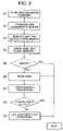
- FIG. 2is a flowchart showing a first embodiment of write processing when the present invention is applied to the memory card in FIG. 1 .
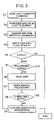
- FIG. 3is a flowchart showing a second embodiment of write processing for the memory card to which the present invention is applied.
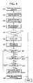
- FIG. 4is a flowchart showing a third embodiment of write processing for the memory card to which the present invention is applied.
- FIG. 5is a flowchart showing a fourth embodiment of write processing for the memory card to which the present invention is applied.
- FIG. 6is a flowchart showing a fifth embodiment of write processing for the memory card to which the present invention is applied.
- FIG. 7is a flowchart showing a sixth embodiment of write processing for the memory card to which the present invention is applied.
- FIG. 8is a block diagram showing an example of the configuration of a memory card to which the second embodiment of write processing of the present invention is applied.
- FIG. 1shows an embodiment of a memory card containing a non-volatile memory according to the present invention.
- a memory card 100 in this embodimentcomprises a flash memory (FLASH) 110 from which a predetermined amount of data may be electrically erased at a time, a microprocessor (CPU) 120 that controls the whole internal operations of the card, such as data transfer, based on externally supplied commands, an interface circuit 130 that transfers signals to and from external devices, a buffer memory 140 , including a RAM and so on, that stores write data sent from external devices and read data sent from the flash memory 110 , an error-correction-code generation & error correction circuit 150 that generates an error correction code for write data and that checks and corrects read data based on the error correction code, and a flash controller 160 that controls writing data to and reading data from the flash memory 110 in response to an instruction from the CPU 120 .
- FLASHflash memory
- CPUmicroprocessor
- the components of the memory cardeach includes a semiconductor integrated circuit. Those semiconductor integrated circuits, which are mounted on a printed circuit board, are molded with resin to form the memory card 100 .
- the external terminals 171 – 175are electrically connected to the circuit of an external electronic device when the memory card is inserted into the card slot of the external electronic device.
- the external terminals 171 and 172are the power terminal and the ground terminal that are connected to the power potential Vcc and the ground potential GND, respectively.
- the external terminal 173receives a clock signal CK used to time the operation.
- the external terminal 174is a terminal through which a command or an address sent from an external host CPU to the card is input and through which the contents of the status register are output from the card to the host CPU.
- the external terminal 175is a terminal through which write data sent from the external host CPU to the card is input and through which data read from the card is output to the host CPU.
- the buffer memory 140comprises a plurality of banks.
- the bank specification signal and the read/write indication signalare supplied from the microprocessor 120 to the buffer memory 140 .
- the bank status indication signalis supplied from the buffer memory 140 to the microprocessor 120 .
- Write data transferred from the external host CPUis stored sequentially in the specified bank in the buffer memory 140 and, via the error-correction-code generation & error correction circuit 150 , supplied to the flash memory 110 .
- the microprocessor 120converts a logical address entered from the external terminal 174 to a physical address and supplies the converted address to the flash memory 110 via the flash controller 160 .
- the synchronization clock SCis supplied from the microprocessor 120 to the error-correction-code generation & error correction circuit 150 , and the signal indicating whether or not an error has been successfully corrected is supplied from the error-correction-code generation & error correction circuit 150 to the microprocessor 120 .
- the interface circuit 130includes a status register SR 1 that contains an indicator indicating the status of the card, for example, whether or not write data has been transferred from the buffer memory 140 to the flash memory 110 .
- the status of the cardis set in the status register SR 1 by a signal from the microprocessor 120 .
- the status bits of the status register SR 1include, for example, an error bit indicating that a write error has occurred, a ready/busy bit indicating that the card may be accessed, and an overflow bit indicating that the buffer memory 140 is full.
- the contents of the status register SR 1may be read by a register read command, sent from the external host CPU, via the external terminal 174 via which the command is input.
- the memory cardmay also be configured such that the status of the flash memory 110 is written directly into the status register SR 1 by a signal sent from the flash controller 160 .
- the flash memory 110comprises a memory array that is a matrix of non-volatile storage devices including insulated-gate field effect transistors each with a floating gate, a word decoder that decodes an externally supplied address signal and activates the corresponding word line in the memory array to set it to the selection level, a data latch connected to the bit lines within the memory array to hold read/write data, and a boosting circuit that generates a high voltage required for writing and erasure.
- the data latchshould be large enough to store data of one sector, that is, data of all storage devices connected to one word line.
- the flash memory 110contains a status register SR 2 that indicates whether data has been written normally or an error has occurred.
- the flash memory used in the memory card in this embodimentis built such that it performs operation based on commands and control signals.
- Commands that may be issued to the flash memoryinclude a read command, a write command, and an erase command.
- Control signals that are sent to the flash memory 110include a chip select signal CE, a write control signal WE indicating whether the operation is a read operation or a write operation, an output control signal OE that indicates a time at which data is output, a system clock SC, and a command enable signal CDE that indicates which input has been received, command or address.
- Those commands and control signalsare given by the flash controller 160 .
- the flash controller 160has a control register.
- the microprocessor 120sets up this control register to cause the flash controller 160 to control the operations, such as a write, read, and erase, to be performed for the flash memory 110 .
- Signals supplied from the microprocessor 120 to the flash controller 160include a control signal indicating which operation, read or write, is to be performed, an address signal specifying the control register and so on, and a data signal indicating data to be stored in the control register.
- the configuration of a memory card on which a flash memory is mountedis not limited to that shown in FIG. 1 .
- the memory cardmay use a flash memory that contains the error-correction-code generation & error correction circuit or may use a chip that combines the error-correction-code generation & error correction circuit with the controller.
- the flash memory 110may be either a binary flash memory in which one-bit data is stored in one storage device or a multi-valued flash memory in which multiple-bit data is stored in one storage device by controlling the threshold voltage.
- multiple flash memoriesmay be mounted.
- ECC circuitsmay be provided, one for each chip, or one ECC circuit may be shared among multiple flash memories.
- the memory card in this embodimenthas two controllers, that is, microprocessor 120 and flash controller 160 , the memory card may have only one of them.
- a data transfer commandis first sent from an external host CPU to the memory card (step S 1 ). Then, write data is transferred from the host CPU to the memory card.
- the transferred commandis supplied to the microprocessor 120 via the interface 130 , and the transferred data is stored in the buffer memory 140 via the interface 130 (step S 2 ).
- the command and the data described aboveare transferred serially.
- a write addressis sent with the command.
- the write datais then transferred from the buffer memory 140 to the flash memory 110 (step S 3 ).
- the datais transferred in parallel, eight bits at a time.
- the write datais transferred via the error-correction-code generation & error correction circuit 150 , with the result that an error correction code is added every 512 bytes before the data is supplied to the flash memory 110 .
- step S 4the data is written in the flash memory 110 , one sector at a time.
- the status register SR 2 in the flash memory 110indicates whether the write operation ended normally or an error occurred.
- the status registeris checked for a write error (step S 5 ). If no error is found, one write operation ends.
- step S 7data is read from the sector of the flash memory 110 where the error occurred in the next step, S 6 .
- the data that was readis sent to the error-correction-code generation & error correction circuit 150 for error correction processing (step S 7 ).
- the error-correction-code generation & error correction circuit 150supplies a signal, which indicates whether or not the error has been successfully corrected, to the microprocessor 120 to allow it to judge whether the error can be corrected (step S 8 ). If it is judged that the error can be corrected, one write operation ends. If it is judged that the error cannot be corrected, substitute processing is performed to write data into some other sector (step S 9 ) and then the write operation ends.
- This substitute processingis performed by writing the write data, stored in the data latch in the flash memory 110 , directly into an alternate sector.
- This methodeliminates the need for supplying write data again to the flash memory 110 ; only the write operation command and the alternate sector address need be supplied. It is also possible to supply the write data, stored in the buffer memory 140 , to the flash memory 110 again when substitute processing is performed.
- the write operationsuccessfully ends if the error correction circuit can correct the error. Only when the error cannot be corrected, write data is written in some other sector. Therefore, as compared with a method in which substitute processing is always performed when a write error occurs, the method used in this embodiment significantly reduces the number of times substitute processing is performed and, therefore, significantly reduces the time required to write data into the flash memory.
- This embodimentmay be used when the status register SR 2 in the flash memory 110 has the following flags: a flag indicating that a general write error has occurred when there is a bit whose threshold voltage does not reach a predetermined level at write time and a flag indicating that a recoverable error, such as an excessive write error, has occurred when there is a bit whose threshold voltage exceeds a predetermined level at write time.
- step S 11that follows step S 5 in the flowchart in FIG. 2 .
- the flag in status register SR 2are checked to determine whether to correct an error with the error correction circuit.
- the excessive write error flagis checked to see if there is a bit whose threshold voltage exceeds a predetermined level at write time.
- a checkis made in steps S 6 –S 8 if the error correction circuit can correct the error and, only when the error correction circuit cannot correct the error, substitute processing is performed.
- step S 9determines the amount of the error with the error correction circuit.
- a bit where an excessive write error occursis a bit that may be recovered to a normal bit, while a bit where the threshold voltage does not reach a predetermined level at write time is a defective bit that cannot be recovered.
- the write processing method in this embodimentimmediately performs substitute processing for a sector where a write error is generated by an unrecoverable, defective bit and, then, bypasses steps S 6 –S 8 to reduce the time required for writing data.
- the write erroris an excessive write error generated by a recoverable bit where the threshold voltage exceeds a predetermined level
- a checkis made in steps S 6 –S 8 if the error correction circuit can correct the error and, only when the error correction circuit cannot correct the error, substitute processing is performed. Therefore, as compared with the method in which substitute processing is always performed when a write error occurs, the method in this embodiment significantly reduces the number of times substitute processing is performed and significantly reduces the time required for writing data into the flash memory as in the first embodiment.
- This embodimentincludes recovery processing for a so-called retention defect bit that is generated when the threshold voltage is out of a predetermined range because data has not been rewritten for a long time.
- a part of write processing in this embodimentis the same as that of write processing in the first embodiment shown in FIG. 2 .
- the only differenceis retention defect recovery processing in steps S 21 –S 23 that are inserted between steps S 8 and S 9 in the flowchart in FIG. 2 .
- a predetermined number nfor example, 2.
- Refresh write processingrefers to processing in which data is read from a particular sector, the data is corrected by the error correction circuit, and then the data is written back into the sector from which it was read.
- the storage devices in the sectorare once erased before data is written back. By performing this processing, a bit where a read error was generated by a retention defect error is recovered and correct data may be written in the flash memory.
- the read data corrected by the error-correction-code generation & error correction circuit 150is once stored in the buffer memory 140 and then transferred to the flash memory 110 .
- the error-correction-code generation & error correction circuit 150 in this embodimentperforms error correction processing, 512 bytes (that is, one quarter of data in a sector) at a time.
- “n” in step S 21 and “m” in step S 22are each the unit of 512-byte data for which error processing is to be performed.
- steps S 21 and S 22error checking is performed for each 512-byte data at a time.
- the error correction circuit used in this embodimentpreferably has a function for outputting the number of error-corrected bits.
- This embodimentmay also be applied to an error correction circuit with no such function because the number of error-corrected bits may be found by inspecting how many times the one-bit error correction circuit is used.
- FIG. 4is advantageously applied when all data in one sector is rewritten, while the modified embodiment in FIG. 5 is used to recover retention defect bits included in the no-rewrite data when data less than one sector in size is rewritten.
- steps S 21 and S 22 in the flowchart in FIG. 4are used instead of steps S 21 and S 22 in the flowchart in FIG. 4 ; that is, steps 24 and 25 in which data is read from the same sector again and error correction is performed, step S 26 in which a check is made for no-rewrite data in the sector if error checking was performed for it, step S 27 in which corrected data stored in the buffer is transferred to the flash memory 110 when error correction was performed, and step S 28 in which refresh write processing is executed with corrected data. If it is found that no error processing was performed for no-rewrite data in step S 26 , the write operation on the sector is ended immediately.
- Steps S 1 to S 8 of the write processing in this embodimentare the same as those of the write processing in the first embodiment in FIG. 2 .
- the only differenceis that, if the error correction circuit judges in step S 8 that an error can be corrected, a check is made in the next step, S 31 , in this embodiment if the number of times of error corrections is larger or smaller than a predetermined number k (for example, 10). If the number of times of error corrections is smaller than the predetermined number, the error counter is incremented in the next step, S 32 , and the write operation is ended immediately. On the other hand, if the number of times of error corrections is larger than the predetermined number k, control is passed to step S 9 to perform substitute processing.
- a predetermined number kfor example, 10
- This embodimentperforms substitute processing when the number of error corrections exceeds the predetermined number k to substitute some other sector for a sector containing a bit where an excessive write error occurs frequently. This method reduces the number of write errors that are generated by such a bit, eliminates the need for the error correction circuit to check if the error can be corrected, and reduces the time required for writing.
- step S 32the number of error corrections that has been counted is stored in the management area of the sector in the flash memory 110 in this embodiment.
- the embodimentis not limited to this configuration.
- the number of error correctionsmay be stored in some other area in the flash memory, in the buffer memory 140 , or in the CPU 120 .
- step S 41in which a read-data-supply path to the buffer memory 140 is blocked, is inserted in this embodiment between step S 5 in which a check is made for an error and step S 6 in which data is read from the flash memory.
- step S 8a check is made in step S 8 if the error correction circuit 150 can correct the error and, only when the circuit cannot correct the error, substitute processing is performed. This is because, unlike the embodiments in FIG. 4 and FIG. 5 , the refresh write processing is not performed in this embodiment and therefore data, read from the flash memory, need not be stored in the buffer memory.
- blocking the read-data-supply path to the buffer memory 140 as in this embodiment before reading data from the flash memoryprevents the read data from occupying a part of the buffer memory 140 .
- Thisallows the CPU 120 to use a free buffer memory to write data into the flash memory and to get the next write data concurrently, thus reducing the time required for writing.
- this embodimentmay be configured as described below. That is, a logic circuit, such as a NAND gate G 1 , is provided to calculate the logical product, for example, between the output control signal OE output from the flash controller 160 to the flash memory 110 and the read path block signal PC output from the CPU 120 . This configuration causes the output signal from this NAND gate G 1 to block the transmission gate TG.
- a logic circuitsuch as a NAND gate G 1
- the error correction method used by the error-correction-code generation & error correction circuit 150may be any method including the one using the Reed Solomon code, Hamming code, or BCH code.
- the buffer memoryis not always required except in the sixth embodiment.
- a memory card not containing a buffer memorymay be used in other embodiments of the present invention.
- the invention made by the inventoris described primarily for a memory card containing a flash memory that is in the background field of the invention.
- the present inventionis not limited to the memory card described above.
- the present inventionmay be applied also to EEPROM chips, other non-volatile memories, memory cards containing such memories, and a memory module including a board on which a plurality of non-volatile memory chips are mounted.
- the storage devicewhen a write error occurs in a card storage device containing a non-volatile memory and an error correction circuit but the error can be corrected by the error correction circuit, the storage device does not perform substitute processing in which data is written in some other address. This reduces the time required for writing and, at the same time, prevents rewrite durability from decreasing rapidly.
Landscapes
- Engineering & Computer Science (AREA)
- Theoretical Computer Science (AREA)
- Quality & Reliability (AREA)
- Physics & Mathematics (AREA)
- General Engineering & Computer Science (AREA)
- General Physics & Mathematics (AREA)
- Techniques For Improving Reliability Of Storages (AREA)
- Read Only Memory (AREA)
- For Increasing The Reliability Of Semiconductor Memories (AREA)
Abstract
Description
Claims (3)
Priority Applications (2)
| Application Number | Priority Date | Filing Date | Title |
|---|---|---|---|
| US11/152,101US7102943B2 (en) | 2001-09-06 | 2005-06-15 | Non-volatile semiconductor memory device |
| US11/453,926US7403436B2 (en) | 2001-09-06 | 2006-06-16 | Non-volatile semiconductor memory device |
Applications Claiming Priority (5)
| Application Number | Priority Date | Filing Date | Title |
|---|---|---|---|
| JP2001-270013 | 2001-09-06 | ||
| JP2001270013AJP4034949B2 (en) | 2001-09-06 | 2001-09-06 | Nonvolatile semiconductor memory device |
| US10/078,471US6608784B2 (en) | 2001-09-06 | 2002-02-21 | Non-volatile semiconductor memory device |
| US10/616,955US6917547B2 (en) | 2001-09-06 | 2003-07-11 | Non-volatile semiconductor memory device |
| US11/152,101US7102943B2 (en) | 2001-09-06 | 2005-06-15 | Non-volatile semiconductor memory device |
Related Parent Applications (1)
| Application Number | Title | Priority Date | Filing Date |
|---|---|---|---|
| US10/616,955ContinuationUS6917547B2 (en) | 2001-09-06 | 2003-07-11 | Non-volatile semiconductor memory device |
Related Child Applications (1)
| Application Number | Title | Priority Date | Filing Date |
|---|---|---|---|
| US11/453,926ContinuationUS7403436B2 (en) | 2001-09-06 | 2006-06-16 | Non-volatile semiconductor memory device |
Publications (2)
| Publication Number | Publication Date |
|---|---|
| US20050246574A1 US20050246574A1 (en) | 2005-11-03 |
| US7102943B2true US7102943B2 (en) | 2006-09-05 |
Family
ID=19095728
Family Applications (4)
| Application Number | Title | Priority Date | Filing Date |
|---|---|---|---|
| US10/078,471Expired - LifetimeUS6608784B2 (en) | 2001-09-06 | 2002-02-21 | Non-volatile semiconductor memory device |
| US10/616,955Expired - LifetimeUS6917547B2 (en) | 2001-09-06 | 2003-07-11 | Non-volatile semiconductor memory device |
| US11/152,101Expired - Fee RelatedUS7102943B2 (en) | 2001-09-06 | 2005-06-15 | Non-volatile semiconductor memory device |
| US11/453,926Expired - Fee RelatedUS7403436B2 (en) | 2001-09-06 | 2006-06-16 | Non-volatile semiconductor memory device |
Family Applications Before (2)
| Application Number | Title | Priority Date | Filing Date |
|---|---|---|---|
| US10/078,471Expired - LifetimeUS6608784B2 (en) | 2001-09-06 | 2002-02-21 | Non-volatile semiconductor memory device |
| US10/616,955Expired - LifetimeUS6917547B2 (en) | 2001-09-06 | 2003-07-11 | Non-volatile semiconductor memory device |
Family Applications After (1)
| Application Number | Title | Priority Date | Filing Date |
|---|---|---|---|
| US11/453,926Expired - Fee RelatedUS7403436B2 (en) | 2001-09-06 | 2006-06-16 | Non-volatile semiconductor memory device |
Country Status (2)
| Country | Link |
|---|---|
| US (4) | US6608784B2 (en) |
| JP (1) | JP4034949B2 (en) |
Cited By (4)
| Publication number | Priority date | Publication date | Assignee | Title |
|---|---|---|---|---|
| US20080184086A1 (en)* | 2007-01-29 | 2008-07-31 | Sun Kwon Kim | Semiconductor memory system performing data error correction using flag cell array of buffer memory |
| US20080307172A1 (en)* | 2007-02-23 | 2008-12-11 | Takashi Abe | System and method for reproducing memory error |
| US8122322B2 (en) | 2007-07-31 | 2012-02-21 | Seagate Technology Llc | System and method of storing reliability data |
| US8352833B2 (en)* | 2007-10-17 | 2013-01-08 | Micron Technology, Inc. | System and method for data read of a synchronous serial interface NAND |
Families Citing this family (50)
| Publication number | Priority date | Publication date | Assignee | Title |
|---|---|---|---|---|
| KR100473308B1 (en)* | 1995-01-31 | 2005-03-14 | 가부시끼가이샤 히다치 세이사꾸쇼 | Nonvolatile memory device |
| US7162600B2 (en) | 2005-03-29 | 2007-01-09 | Hitachi, Ltd. | Data copying method and apparatus in a thin provisioned system |
| JP2003228511A (en)* | 2002-02-04 | 2003-08-15 | Elpida Memory Inc | Data writing method and memory system |
| JP4550439B2 (en)* | 2003-02-28 | 2010-09-22 | 東芝メモリシステムズ株式会社 | ECC controller |
| JP2005056394A (en) | 2003-07-18 | 2005-03-03 | Toshiba Corp | Storage device and memory card |
| JP2005331559A (en)* | 2004-05-18 | 2005-12-02 | Matsushita Electric Ind Co Ltd | Image signal processing device |
| WO2005111812A1 (en)* | 2004-05-19 | 2005-11-24 | Matsushita Electric Industrial Co., Ltd. | Memory control circuit, nonvolatile storage apparatus, and memory control method |
| JP2006023957A (en)* | 2004-07-07 | 2006-01-26 | Sony Corp | Semiconductor integrated circuit and information processor |
| JP2006107363A (en)* | 2004-10-08 | 2006-04-20 | Toshiba Corp | Portable electronic device and memory access method used for portable electronic device |
| US8083942B2 (en)* | 2004-12-06 | 2011-12-27 | Board of Regents of the Nevada System of Higher Education, on Behalf of the Universary of Nevada, Reno | Systems and methods for purification of liquids |
| JP4842563B2 (en) | 2005-05-16 | 2011-12-21 | パナソニック株式会社 | MEMORY CONTROLLER, NONVOLATILE MEMORY DEVICE, NONVOLATILE MEMORY SYSTEM, AND DATA WRITE METHOD |
| JP4699808B2 (en)* | 2005-06-02 | 2011-06-15 | 株式会社日立製作所 | Storage system and configuration change method |
| KR100648290B1 (en) | 2005-07-26 | 2006-11-23 | 삼성전자주식회사 | Nonvolatile memory device and its programming method which can improve program speed |
| WO2007028109A2 (en)* | 2005-09-02 | 2007-03-08 | Metaram, Inc. | Methods and apparatus of stacking drams |
| JP4813264B2 (en)* | 2006-06-14 | 2011-11-09 | 株式会社日立製作所 | Storage system |
| JP4908083B2 (en)* | 2006-06-30 | 2012-04-04 | 株式会社東芝 | Memory controller |
| US7844878B2 (en)* | 2006-08-09 | 2010-11-30 | Microsoft Corporation | Dynamic electronic correction code feedback to extend memory device lifetime |
| KR100894809B1 (en)* | 2006-09-22 | 2009-04-24 | 삼성전자주식회사 | Memory system and its program method |
| KR100845526B1 (en)* | 2006-10-19 | 2008-07-10 | 삼성전자주식회사 | Memory system including flash memory and program method thereof |
| KR100926475B1 (en)* | 2006-12-11 | 2009-11-12 | 삼성전자주식회사 | Multi bit flash memory device and its program method |
| US7958390B2 (en)* | 2007-05-15 | 2011-06-07 | Sandisk Corporation | Memory device for repairing a neighborhood of rows in a memory array using a patch table |
| WO2008143815A1 (en)* | 2007-05-15 | 2008-11-27 | Sandisk Corporation | Memory device and method for repairing a neighborhood of rows in a memory array using a patch table |
| US7966518B2 (en)* | 2007-05-15 | 2011-06-21 | Sandisk Corporation | Method for repairing a neighborhood of rows in a memory array using a patch table |
| US7765426B2 (en) | 2007-06-07 | 2010-07-27 | Micron Technology, Inc. | Emerging bad block detection |
| JP4417994B2 (en)* | 2007-11-26 | 2010-02-17 | 株式会社東芝 | Material data recording apparatus and material data recording method |
| KR100933859B1 (en)* | 2007-11-29 | 2009-12-24 | 주식회사 하이닉스반도체 | Flash memory device and its program method |
| JP2009181439A (en)* | 2008-01-31 | 2009-08-13 | Toshiba Corp | Memory system |
| EP2249243B1 (en)* | 2008-02-08 | 2014-06-18 | Fujitsu Limited | Backup method, disc array device, and controller |
| US8028244B2 (en)* | 2008-02-21 | 2011-09-27 | Brother Kogyo Kabushiki Kaisha | Status processing system, status processor, and status displaying method |
| JP2009266258A (en) | 2008-04-22 | 2009-11-12 | Hitachi Ltd | Semiconductor device |
| KR20100012605A (en)* | 2008-07-29 | 2010-02-08 | 삼성전자주식회사 | Non-volatile memory device and method for program using ecc |
| JP5306745B2 (en)* | 2008-09-05 | 2013-10-02 | ハギワラソリューションズ株式会社 | Flash memory management method and flash memory device |
| US8438455B2 (en)* | 2008-12-31 | 2013-05-07 | Intel Corporation | Error correction in a solid state disk |
| US20100195393A1 (en)* | 2009-01-30 | 2010-08-05 | Unity Semiconductor Corporation | Data storage system with refresh in place |
| KR101005164B1 (en)* | 2009-05-29 | 2011-01-04 | 주식회사 하이닉스반도체 | Nonvolatile Memory Device and Its Program Method |
| JP5503960B2 (en)* | 2009-12-25 | 2014-05-28 | 三星電子株式会社 | Nonvolatile semiconductor memory device |
| US9142323B1 (en)* | 2011-03-01 | 2015-09-22 | Sk Hynix Memory Solutions Inc. | Hardware acceleration of DSP error recovery for flash memory |
| JP5813450B2 (en)* | 2011-10-17 | 2015-11-17 | 日立オートモティブシステムズ株式会社 | Electronic control unit |
| JP2013131192A (en)* | 2011-12-22 | 2013-07-04 | Fujitsu Ltd | Storage device and method for controlling storage device |
| JP2012190538A (en)* | 2012-05-25 | 2012-10-04 | Toshiba Corp | Storage device, storage medium reproducing method, storage medium reproducing program |
| US9098105B2 (en)* | 2012-08-24 | 2015-08-04 | Avago Technologies General Ip (Singapore) Pte. Ltd. | Dynamic Y-buffer size adjustment for retained sector reprocessing |
| US9110829B2 (en)* | 2012-11-30 | 2015-08-18 | Taiwan Semiconductor Manufacturing Co. Ltd. | MRAM smart bit write algorithm with error correction parity bits |
| JP5548789B2 (en)* | 2013-01-22 | 2014-07-16 | 株式会社日立製作所 | Semiconductor device |
| JP2015118499A (en) | 2013-12-18 | 2015-06-25 | ソニー株式会社 | Storage apparatus, memory controller, control method for storage apparatus, and program |
| WO2015182439A1 (en) | 2014-05-26 | 2015-12-03 | ソニー株式会社 | Storage device, storage system, and storage device control method |
| KR102289001B1 (en)* | 2014-06-09 | 2021-08-13 | 삼성전자주식회사 | Solid state drive and operation method thereof |
| US9772901B2 (en)* | 2015-05-08 | 2017-09-26 | Nxp Usa, Inc. | Memory reliability using error-correcting code |
| US10656991B2 (en)* | 2015-08-24 | 2020-05-19 | International Business Machines Corporation | Electronic component having redundant product data stored externally |
| US10546625B2 (en) | 2016-09-27 | 2020-01-28 | Spin Memory, Inc. | Method of optimizing write voltage based on error buffer occupancy |
| US11086715B2 (en)* | 2019-01-18 | 2021-08-10 | Arm Limited | Touch instruction |
Citations (10)
| Publication number | Priority date | Publication date | Assignee | Title |
|---|---|---|---|---|
| JPH06131886A (en) | 1992-10-14 | 1994-05-13 | Toshiba Corp | Semiconductor filing device |
| US5532962A (en) | 1992-05-20 | 1996-07-02 | Sandisk Corporation | Soft errors handling in EEPROM devices |
| JPH08279295A (en) | 1995-04-05 | 1996-10-22 | Toshiba Corp | Storage system including non-volatile semiconductor storage unit |
| US5778418A (en) | 1991-09-27 | 1998-07-07 | Sandisk Corporation | Mass computer storage system having both solid state and rotating disk types of memory |
| US5907856A (en) | 1995-07-31 | 1999-05-25 | Lexar Media, Inc. | Moving sectors within a block of information in a flash memory mass storage architecture |
| US5991517A (en)* | 1989-04-13 | 1999-11-23 | Sandisk Corporation | Flash EEprom system with cell by cell programming verification |
| US6046935A (en) | 1996-03-18 | 2000-04-04 | Kabushiki Kaisha Toshiba | Semiconductor device and memory system |
| US6134631A (en)* | 1996-08-19 | 2000-10-17 | Hyundai Electronics America, Inc. | Non-volatile memory with embedded programmable controller |
| US6134143A (en) | 1997-12-01 | 2000-10-17 | Micron Technology, Inc. | Multi-state flash memory defect management |
| US6349056B1 (en) | 2000-12-28 | 2002-02-19 | Sandisk Corporation | Method and structure for efficient data verification operation for non-volatile memories |
Family Cites Families (6)
| Publication number | Priority date | Publication date | Assignee | Title |
|---|---|---|---|---|
| US5657332A (en)* | 1992-05-20 | 1997-08-12 | Sandisk Corporation | Soft errors handling in EEPROM devices |
| DE69716233T2 (en) | 1996-08-16 | 2003-02-20 | Tokyo Electron Device Ltd., Yokohama | SEMICONDUCTOR MEMORY ARRANGEMENT WITH ERROR DETECTION AND CORRECTION |
| US5771346A (en)* | 1996-10-24 | 1998-06-23 | Micron Quantum Devices, Inc. | Apparatus and method for detecting over-programming condition in multistate memory device |
| JP3589033B2 (en) | 1998-06-25 | 2004-11-17 | 東京エレクトロンデバイス株式会社 | Flash memory system |
| JP2000173289A (en) | 1998-12-10 | 2000-06-23 | Toshiba Corp | Error-correctable flash memory system |
| US6266273B1 (en)* | 2000-08-21 | 2001-07-24 | Sandisk Corporation | Method and structure for reliable data copy operation for non-volatile memories |
- 2001
- 2001-09-06JPJP2001270013Apatent/JP4034949B2/ennot_activeExpired - Fee Related
- 2002
- 2002-02-21USUS10/078,471patent/US6608784B2/ennot_activeExpired - Lifetime
- 2003
- 2003-07-11USUS10/616,955patent/US6917547B2/ennot_activeExpired - Lifetime
- 2005
- 2005-06-15USUS11/152,101patent/US7102943B2/ennot_activeExpired - Fee Related
- 2006
- 2006-06-16USUS11/453,926patent/US7403436B2/ennot_activeExpired - Fee Related
Patent Citations (10)
| Publication number | Priority date | Publication date | Assignee | Title |
|---|---|---|---|---|
| US5991517A (en)* | 1989-04-13 | 1999-11-23 | Sandisk Corporation | Flash EEprom system with cell by cell programming verification |
| US5778418A (en) | 1991-09-27 | 1998-07-07 | Sandisk Corporation | Mass computer storage system having both solid state and rotating disk types of memory |
| US5532962A (en) | 1992-05-20 | 1996-07-02 | Sandisk Corporation | Soft errors handling in EEPROM devices |
| JPH06131886A (en) | 1992-10-14 | 1994-05-13 | Toshiba Corp | Semiconductor filing device |
| JPH08279295A (en) | 1995-04-05 | 1996-10-22 | Toshiba Corp | Storage system including non-volatile semiconductor storage unit |
| US5907856A (en) | 1995-07-31 | 1999-05-25 | Lexar Media, Inc. | Moving sectors within a block of information in a flash memory mass storage architecture |
| US6046935A (en) | 1996-03-18 | 2000-04-04 | Kabushiki Kaisha Toshiba | Semiconductor device and memory system |
| US6134631A (en)* | 1996-08-19 | 2000-10-17 | Hyundai Electronics America, Inc. | Non-volatile memory with embedded programmable controller |
| US6134143A (en) | 1997-12-01 | 2000-10-17 | Micron Technology, Inc. | Multi-state flash memory defect management |
| US6349056B1 (en) | 2000-12-28 | 2002-02-19 | Sandisk Corporation | Method and structure for efficient data verification operation for non-volatile memories |
Cited By (8)
| Publication number | Priority date | Publication date | Assignee | Title |
|---|---|---|---|---|
| US20080184086A1 (en)* | 2007-01-29 | 2008-07-31 | Sun Kwon Kim | Semiconductor memory system performing data error correction using flag cell array of buffer memory |
| US8055978B2 (en)* | 2007-01-29 | 2011-11-08 | Samsung Electronics Co., Ltd. | Semiconductor memory system performing data error correction using flag cell array of buffer memory |
| US20080307172A1 (en)* | 2007-02-23 | 2008-12-11 | Takashi Abe | System and method for reproducing memory error |
| US7921341B2 (en)* | 2007-02-23 | 2011-04-05 | Nec Corporation | System and method for reproducing memory error |
| US8122322B2 (en) | 2007-07-31 | 2012-02-21 | Seagate Technology Llc | System and method of storing reliability data |
| US8352833B2 (en)* | 2007-10-17 | 2013-01-08 | Micron Technology, Inc. | System and method for data read of a synchronous serial interface NAND |
| US8694860B2 (en)* | 2007-10-17 | 2014-04-08 | Micron Technology, Inc. | System and method for data read of a synchronous serial interface NAND |
| US9235546B2 (en) | 2007-10-17 | 2016-01-12 | Micron Technology, Inc. | System and method for data read of a synchronous serial interface NAND |
Also Published As
| Publication number | Publication date |
|---|---|
| US7403436B2 (en) | 2008-07-22 |
| US20040008554A1 (en) | 2004-01-15 |
| US20050246574A1 (en) | 2005-11-03 |
| JP2003076615A (en) | 2003-03-14 |
| JP4034949B2 (en) | 2008-01-16 |
| US6608784B2 (en) | 2003-08-19 |
| US20060233032A1 (en) | 2006-10-19 |
| US20030043647A1 (en) | 2003-03-06 |
| US6917547B2 (en) | 2005-07-12 |
Similar Documents
| Publication | Publication Date | Title |
|---|---|---|
| US7102943B2 (en) | Non-volatile semiconductor memory device | |
| US7116578B2 (en) | Non-volatile memory device and data storing method | |
| US7958430B1 (en) | Flash memory device and method | |
| US8125825B2 (en) | Memory system protected from errors due to read disturbance and reading method thereof | |
| US7881133B2 (en) | Method of managing a flash memory and the flash memory | |
| US7305596B2 (en) | Nonvolatile memory and nonvolatile memory apparatus | |
| US6388919B2 (en) | Memory controller for flash memory system and method for writing data to flash memory device | |
| KR101563647B1 (en) | Memory system and data processing method thereof | |
| US8607120B2 (en) | Semiconductor memory device for performing additional ECC correction according to cell pattern and electronic system including the same | |
| US20080172521A1 (en) | Memory System Determining Storage Mode According to Host Provided Data Information | |
| US20060171210A1 (en) | Nonvolatile semiconductor memory device which uses some memory blocks in multilevel memory as binary memory blocks | |
| US20080172520A1 (en) | Nonvolatile memory devices including multiple user-selectable program modes and related methods of operation | |
| US8516354B2 (en) | Method for reducing uncorrectable errors of a memory device regarding error correction code, and associated memory device and controller thereof | |
| US20140115383A1 (en) | Multiple level cell memory device with single bit per cell, re-mappable memory block | |
| US20060018159A1 (en) | Programmable NAND memory | |
| US20110141811A1 (en) | Semiconductor memory device | |
| US20100287448A1 (en) | Flash memory device with rectifiable redundancy bit and method of controlling the same | |
| CN113535460A (en) | Data storage device and operation method thereof | |
| US20130047056A1 (en) | Flash memory device with rectifiable redundancy and method of controlling the same | |
| JP3482543B2 (en) | Semiconductor memory | |
| CN113674794B (en) | Semiconductor memory device and method for reading error detection and correction related information | |
| US12417814B2 (en) | Storage device for backing up state group data in the event of a sudden power-off and program method thereof | |
| US12436839B2 (en) | Storage device for setting prohibited threshold voltage distribution | |
| JP2006185290A (en) | Memory controller, flash memory system and method for controlling flash memory |
Legal Events
| Date | Code | Title | Description |
|---|---|---|---|
| FEPP | Fee payment procedure | Free format text:PAYOR NUMBER ASSIGNED (ORIGINAL EVENT CODE: ASPN); ENTITY STATUS OF PATENT OWNER: LARGE ENTITY | |
| FPAY | Fee payment | Year of fee payment:4 | |
| AS | Assignment | Owner name:RENESAS ELECTRONICS CORPORATION, JAPAN Free format text:CHANGE OF NAME;ASSIGNOR:NEC ELECTRONICS CORPORATION;REEL/FRAME:026467/0279 Effective date:20100401 Owner name:NEC ELECTRONICS CORPORATION, JAPAN Free format text:MERGER;ASSIGNOR:RENESAS TECHNOLOGY CORP.;REEL/FRAME:026467/0252 Effective date:20100401 | |
| FPAY | Fee payment | Year of fee payment:8 | |
| AS | Assignment | Owner name:RENESAS ELECTRONICS CORPORATION, JAPAN Free format text:ASSIGNMENT OF ASSIGNORS INTEREST;ASSIGNOR:HITACHI ULSI SYSTEMS CO., LTD.;REEL/FRAME:032859/0252 Effective date:20140326 | |
| AS | Assignment | Owner name:RENESAS ELECTRONICS CORPORATION, JAPAN Free format text:CHANGE OF ADDRESS;ASSIGNOR:RENESAS ELECTRONICS CORPORATION;REEL/FRAME:044928/0001 Effective date:20150806 | |
| FEPP | Fee payment procedure | Free format text:MAINTENANCE FEE REMINDER MAILED (ORIGINAL EVENT CODE: REM.) | |
| LAPS | Lapse for failure to pay maintenance fees | Free format text:PATENT EXPIRED FOR FAILURE TO PAY MAINTENANCE FEES (ORIGINAL EVENT CODE: EXP.); ENTITY STATUS OF PATENT OWNER: LARGE ENTITY | |
| STCH | Information on status: patent discontinuation | Free format text:PATENT EXPIRED DUE TO NONPAYMENT OF MAINTENANCE FEES UNDER 37 CFR 1.362 | |
| FP | Lapsed due to failure to pay maintenance fee | Effective date:20180905 |