US7102907B2 - Wavelength division multiplexed memory module, memory system and method - Google Patents
Wavelength division multiplexed memory module, memory system and methodDownload PDFInfo
- Publication number
- US7102907B2 US7102907B2US10/238,322US23832202AUS7102907B2US 7102907 B2US7102907 B2US 7102907B2US 23832202 AUS23832202 AUS 23832202AUS 7102907 B2US7102907 B2US 7102907B2
- Authority
- US
- United States
- Prior art keywords
- optical
- memory
- signals
- wavelength
- memory modules
- Prior art date
- Legal status (The legal status is an assumption and is not a legal conclusion. Google has not performed a legal analysis and makes no representation as to the accuracy of the status listed.)
- Expired - Lifetime
Links
- 230000015654memoryEffects0.000titleclaimsabstractdescription423
- 238000000034methodMethods0.000titleclaimsdescription28
- 230000003287optical effectEffects0.000claimsabstractdescription336
- 230000008878couplingEffects0.000claimsabstractdescription57
- 238000010168coupling processMethods0.000claimsabstractdescription57
- 238000005859coupling reactionMethods0.000claimsabstractdescription57
- 238000004891communicationMethods0.000claimsabstractdescription28
- 239000000758substrateSubstances0.000claimsdescription12
- 238000001514detection methodMethods0.000claimsdescription8
- 230000006870functionEffects0.000claimsdescription5
- 238000013500data storageMethods0.000claimsdescription2
- 239000004020conductorSubstances0.000claims7
- 238000010586diagramMethods0.000description6
- 238000012546transferMethods0.000description2
- 238000013459approachMethods0.000description1
- 238000004364calculation methodMethods0.000description1
- 238000012986modificationMethods0.000description1
- 230000004048modificationEffects0.000description1
- 239000013307optical fiberSubstances0.000description1
- 230000003068static effectEffects0.000description1
- 230000001360synchronised effectEffects0.000description1
Images


Classifications
- G—PHYSICS
- G11—INFORMATION STORAGE
- G11C—STATIC STORES
- G11C5/00—Details of stores covered by group G11C11/00
- G11C5/06—Arrangements for interconnecting storage elements electrically, e.g. by wiring
- G11C5/063—Voltage and signal distribution in integrated semi-conductor memory access lines, e.g. word-line, bit-line, cross-over resistance, propagation delay
Definitions
- This inventionrelates to computer systems, and, more particularly, to a computer system having a memory hub coupling several memory devices to a processor or other memory access device.
- DIMMsdouble in-line memory modules
- FIG. 1An example of a conventional DIMM-type memory module 10 is shown in FIG. 1 .
- the memory module 10includes a circuit board substrate 14 on which several memory devices 20 , typically dynamic random access memories (“DRAMs”), are mounted.
- DRAMsdynamic random access memories
- 8 memory devices 20are mounted on each side of the substrate 14 .
- Terminals 24are formed along an edge of the substrate 14 , which mate with slotted connectors (not shown) typically mounted on a computer system mother-board.
- the terminals 24are electrically coupled to the power and signal terminals on the memory devices 20 .
- a register 26that stores command and address signals applied to the memory module 10 through the terminals 24 responsive to a clock signal that is also applied to the memory module 10 through the terminals 24 .
- the register 26then applies the command and address signals to the memory devices 20 .
- Memory modules having a register 26 operating in this mannerare known as “registered DRAM modules.” However, it should be understood that memory modules often do not include the register 26 , and they may include components in addition to those shown in FIG. 1 .
- a portion of a computer system 30 shown in FIG. 2includes three memory modules 10 a,b,c coupled to a system controller 32 though a common data bus 34 , address bus 36 and command bus 38 .
- the system controller 32initiates a memory operation by coupling a memory request in the form of a memory command and a memory address (generally in the form of a row address and a column address) to all of the memory modules 10 through the command bus 38 and the address bus 36 , respectively. If the memory operation is a write operation, the system controller 32 will also couple write data to the memory modules 10 through the data bus 34 .
- the system controller 32also generally applies a unique chip select or similar select signal to each of the memory modules 10 .
- a unique select signalis thus applied to each of the memory modules 10 so that only the memory module 10 receiving the select signal responds to the memory request.
- the bandwidth of data between the system controller 32 and the memory modules 10could be increased by simultaneously accessing all of the 16 memory devices 20 ( FIG. 1 ) in each of the modules 10 .
- the 16 memory devices 20 included in the memory module 10could be divided into 2 sets or “ranks” of 8 memory devices and both of the ranks could be accessed at the same time, data could be read from the ranks at a rate that is 2 times faster than the rate at which data can be read from each rank of the memory devices 20 .
- datacan be accessed in conventional memory modules 10 only one rank of 6 memory devices 20 at a time.
- the bandwidth of data coupled from the memory modules 10threatens to be limited by the bandwidth of the data bus 34 coupled between the system controller 32 and the memory modules 10 .
- Another factor that limits the operating speed of computer systems using the system controller 32 coupled to the memory modules 10 through the buses 34 - 38is the need to allow for a settling time between writing data to a memory module 10 and reading data from a memory module 10 .
- the system controller 32outputs data to the memory modules, the data signals are reflected from various locations, such as the junction between the data bus 34 and terminals 24 ( FIG. 1 ) on the substrates 14 of the modules 10 . Therefore, signal induced noise is present on the data bus for a considerable period after data have been written to the memory modules 10 .
- Signal induced noiseis generated on the data bus for the same reason in a read operation when one of the memory modules 10 couples data onto the data bus 34 for transfer to the system controller 32 .
- This noisemust be allowed to settle before data are subsequently written to or read from the memory modules 10 or else the noise may be mistakenly interpreted as read or write data.
- the need to provide for a settling timecan markedly reduce the effective memory bandwidth of computer systems and other devices using memory modules.
- a plurality of memory modulesare optically coupled to a controller.
- Each of the memory modulesincludes a plurality of memory devices and an optical memory hub.
- the optical memory hub in each memory moduleis electrically coupled to the memory devices in the module, and includes an optical input/output port coupled to an optical input/output port of the controller.
- the optical memory hub in each memory modulereceives optical input signals and applies corresponding electrical signals to the memory devices in the module.
- the optical memory hub in each memory modulealso receives electrical signals from the memory devices in the module and transmits corresponding optical output signals.
- the optical memory hub in each of the memory modulesreceives or transmits at least some optical signals at a wavelength that is different from the wavelength of at least some optical signals received or transmitted by the optical memory hubs in a plurality of the other memory modules.
- FIG. 1is a plan view of a conventional memory module.
- FIG. 2is a block diagram of a portion of a conventional computer system using several of the memory modules shown in FIG. 1 .
- FIG. 3is a block diagram of a portion of a computer system including a controller and several memory modules according to one example of the present invention.
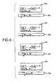
- FIG. 4is a diagram illustrating one example of a communications protocol that can be used to allow the controller and memory modules shown in FIG. 3 to communicate with each other.
- FIG. 5is a diagram illustrating another example of a communications protocol that can be used to allow the controller and memory modules shown in FIG. 3 to communicate with each other.
- FIG. 6is a schematic plan view a memory module showing one example of a technique for programming the module according to invention.
- FIG. 7is a block diagram of a computer system using the controller and memory modules of FIG. 3 according to one example of the invention.
- FIG. 3is a block diagram of a portion of a computer system according to one example of the present invention.
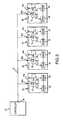
- a controller 40such as a system controller or a memory controller, is coupled to 4 memory modules 44 a-d though an optical communication path 50 , although a greater or less number of modules 44 may be coupled to the controller 40 .
- the controller 40 and the memory modules 44 a-dare coupled to the optical communication path 50 through optical input/output ports 56 , 62 a-d , respectively.
- the controller 40may communicate with the memory modules 44 in any of a variety of communications protocols, but they preferably communicate using optical signal packets that contain data, address and command information.
- the optical communication path 50may be one or more optical waveguides, such as optical fibers or waveguides mounted on printed circuit boards, free space, or some other optical coupling medium that allows light to be transmitted between the controller 40 and the memory modules 44 .
- the controller 40can transmit and receive light at any of a plurality of wavelengths ⁇ .
- the memory modules 44preferably can also transmit and receive light at any of a plurality of wavelengths ⁇ , as will be explained in greater detail below.
- the memory modules 44also preferably have electrical terminals 58 through which at least power may be applied to the memory modules 44 .
- each memory module 44includes a wave-division multiplexed optical hub 70 having an optical port 72 optically coupled to the communication path 50 .
- the optical hub 70can receive light at any of a plurality of wavelengths ⁇ , and it converts the received light into corresponding electrical signals that are applied to a bus system 78 .
- the optical hub 70also receives electrical signals from the bus system 78 , and it converts the received electrical signals to corresponding optical signals, preferably at any of a plurality of wavelengths ⁇ . These optical signals are applied to the optical port 72 and coupled to the controller 40 through the optical communication path.
- the bus system 78couples the optical hub 70 to several memory devices 80 , which may be, for example, synchronous random access memories (“SDRAMs”).
- SDRAMssynchronous random access memories
- the bus system 78may include, for example, separate command, address and data buses, although it may alternatively include a greater or lesser number of buses.
- a single busmay be used to couple one or more packets containing command, address and data bits between the optical hub 70 and the memory devices 80 .
- each memory module 44may also include a volatile or non-volatile memory device 84 , such as an electrically erasable programmable read only memory (“EEPROM”), for storing parameters indicative of the operation of the memory module 44 .
- EEPROMelectrically erasable programmable read only memory
- the memory device 84may store information specifying the wavelength ⁇ the memory module 44 will use to communicate with the controller 40 through the optical communication path 50 .
- the memory device 84is preferably electrically coupled to the optical hub 70 through lines 88 .
- the non-volatile memory device 84may also be programmed through a serial bus (not shown) of the type that is typically used to program EEPROMs in memory modules.
- the parameters of the memory module 44are read by the controller 40 through a bus 52 , which may be either a serial bus or a parallel bus.
- the controller 40may read the parameters from the memory device 84 at power-up, for example, to allow the controller 40 to configure itself in accordance with the parameters of the memory module 44 .
- the optical communication path 50may include a single communication link through which command, address and data signals are coupled, it preferably includes several communication links operating in conjunction with each other.
- a first communication linkmay be used to couple the data signals between the controller 40 and the memory module 44
- a second communication linkmay be used to couple command and address signals from the controller 40 to the memory module 44 .
- the command, data and address signalsare preferably coupled through a conventional communication protocol, such as by sending data packets, time-division multiplexing, etc.
- wavelength division multiplexingis used to allow the controller 40 to selectively communicate with the memory modules.
- a variety of wavelength division multiplexing protocolsmay be used to allow communication between the controller 40 and the memory modules 44 .
- a first wavelength ⁇ 1is used to communicate between the controller 40 and the optical hub 70 in the first memory module 44 a
- a second wavelength ⁇ 2is used to communicate between the controller 40 and the optical hub 70 in the second memory module 44 b
- a third wavelength ⁇ 3is used to communicate between the controller 40 and the optical hub 70 in the third memory module 44 c
- a fourth wavelength ⁇ 4is used to communicate between the controller 40 and the optical hub 70 in the fourth memory module 44 d .
- the controller 40may simultaneously communicate with two or more memory modules 44 , and, in doing so, may be simultaneously performing two or more memory operations of the same type or of different types.
- the controller 40may be simultaneously reading data from the second memory module 44 b using light at the second wavelength ⁇ 2 , and reading data from the fourth memory module 44 d using light at the fourth wavelength ⁇ 4 .
- the controller 40may be writing data to the first memory module 44 a using light at the first wavelength ⁇ 1 at the same time the controller 40 is reading data from the third memory module 44 c using light at the third wavelength ⁇ 3 .
- Use of this protocolis most appropriate where several memory modules 44 are coupled to the controller since there is no advantage to using this protocol of wavelength division multiplexing where a single memory module 44 is coupled to the controller 40 .
- the communications protocol shown in FIG. 5can be used.
- read dataare coupled from a plurality the memory modules 44 using optical signals having a first wavelength ⁇ 1
- write dataare coupled to a plurality the memory modules 44 using optical signals having a second wavelength ⁇ 2 .
- the command and address signalsare coupled to each of the memory modules 44 at different wavelengths. More specifically, as shown in FIG.
- command and address signalsare coupled to the first memory module 44 a at a third wavelength ⁇ 3
- command and address signalsare coupled to the second memory module 44 b at a fourth wavelength ⁇ 4
- command and address signalsare coupled to the third memory module 44 c at a fifth wavelength ⁇ 5
- command and address signalsare coupled to the fourth memory module 44 d at a sixth wavelength ⁇ 6 .
- the advantage of the communication protocol shown in FIG. 5 over the protocol shown in FIG. 4is that the protocol of FIG. 5 allows the controller 40 to read from one memory module, e.g., memory module 44 b , at the same time that the controller 40 is writing to another memory module, e.g., memory module 44 c .
- the protocol shown in FIG. 5does not allow read data to be coupled from two different memory modules 44 at the same time.
- the protocol shown in FIG. 5is best suited to systems having relatively few memory modules 44 and/or processors or other memory access devices because there is less likely to be data bus conflicts in such systems.
- the controller 40may dynamically select a wavelength division multiplexing protocol based on a variety of operating conditions. For example, the controller 40 may select a protocol based on the number of memory modules 44 in a system. For a larger number of memory modules, the wavelength division multiplexing protocol shown in FIG. 4 might be selected. For a smaller number of memory modules, the wavelength division multiplexing protocol shown in FIG. 5 might be selected.
- the controller 40might also select a wavelength division multiplexing protocol based on the nature of the software application currently being executed in a computer system. For example, a graphics intensive application like video games might select one type of wavelength division multiplexing protocol while a computationally intensive application like spreadsheets might select a different wavelength division multiplexing protocol.
- each memory module 44can receive and the wavelength ⁇ of the optical signals each memory module 44 can transmit.
- Each memory module 44can, of course, be fabricated to receive and transmit optical signals having specific wavelengths ⁇ . It would then be necessary to ensure that memory module operating at different wavelengths were present in a computer system or other electronic system. It would be less desirable for two memory modules 44 operating at the same wavelength ⁇ to be present in a system. It is preferable to make all of the memory modules 44 identical, and to program them for different wavelengths after the modules 44 have been installed in a computer system or other electronic system.
- One technique for programming each of several memory modules to operate at respective wavelengths ⁇is to apply at least one wavelength identifying signal to the memory module 44 based on which connector receives the memory module. For example, as shown in FIG. 6 , each of four memory modules 90 a-d is plugged into a respective slotted connector 94 a-d . A number of wavelength identifying terminals 96 are provided at the edge of each of the modules 90 . Each of the connectors 94 has one of several terminals 98 coupled to a predetermined voltage, such as ground, based on the location of the connector 94 .
- the first connector 94 ahas its first terminal 98 coupled to ground
- the second connector 94 bhas its second terminal 98 coupled to ground
- the third connector 94 chas its third terminal 98 coupled to ground
- the fourth connector 94 dhas its fourth terminal 98 coupled to ground.
- Each of the memory modules 44includes a detection circuit 100 coupled to the wavelength identifying terminals 96 and to the optical hub 70 .
- the detection circuitry 100can detect which wavelength identifying terminal 96 is coupled to ground and cause the optical hub 70 in each of the memory modules 90 to transmit and receive optical signals at wavelengths corresponding to the connector 94 in which the memory module 90 is inserted.
- Other encoding schemescould also be used, such as by binary coding the terminals coupled to ground.
- Another approach to programming memory modulesis to program the memory modules upon power-up or at some other time.
- a respective select signalcan be applied sequentially to each of the memory modules 44 ( FIG. 3 ) while to controller 40 outputs an optical signal having the wavelength ⁇ that the memory module 44 will transmit and/or receive.
- an optical signal having a wavelength of ⁇ 1may be transmitted by the controller 40 while the controller 40 applies a select signal to the first memory module 44 a .
- the controller 40then outputs an optical signal having a wavelength of ⁇ 2 while applying a select signal to the second memory module 44 b , etc.
- the first memory module 44 awill transmit and receive optical signals having the first wavelength ⁇ 1
- the second memory module 44 bwill transmit and receive optical signals having the first wavelength ⁇ 2 .
- Other means of programming the memory modules 44 to receive and transmit light at respective wavelengthswill be apparent to one skilled in the art.
- the memory modules 44may also be programmed through a serial bus (not shown) of the type that is typically used to program EEPROMs in memory modules.
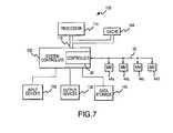
- FIG. 7A computer system 110 using the controller 40 and memory modules 44 of FIG. 3 according to one example of the invention is shown in FIG. 7 .
- the computer system 110includes a processor 114 for performing various computing functions, such as executing specific software to perform specific calculations or tasks.
- the processor 114includes a processor bus 118 that normally includes an address bus, a control bus, and a data bus.
- the computer system 110includes a system controller 120 that is coupled to the processor bus 118 .
- the system controller 120also includes the controller 40 , which is, in turn, optically coupled to memory modules 44 a-d through the optical communication path 50 .
- the controller 40may be external to the system controller 120 and coupled to it or some other component in the computer system 110 , such as the processor 114 .
- the computer system 110includes one or more input devices 130 , such as a keyboard or a mouse, coupled to the processor 114 through the system controller 120 to allow an operator to interface with the computer system 110 .
- the computer system 110also includes one or more output devices 134 coupled to the processor 114 through the system controller 120 , such output devices typically being a printer or a video terminal.
- One or more data storage devices 140are also typically coupled to the processor 114 through the system controller 120 to allow the processor 114 to store data or retrieve data from internal or external storage media (not shown). Examples of typical storage devices 140 include hard and floppy disks, tape cassettes, and compact disk read-only memories (CD-ROMs).
- the processor 114is also typically coupled to cache memory 144 , which is usually static random access memory (“SRAM”).
- SRAMstatic random access memory
Landscapes
- Optical Communication System (AREA)
Abstract
Description
Claims (63)
Priority Applications (2)
| Application Number | Priority Date | Filing Date | Title |
|---|---|---|---|
| US10/238,322US7102907B2 (en) | 2002-09-09 | 2002-09-09 | Wavelength division multiplexed memory module, memory system and method |
| US10/893,709US7106611B2 (en) | 2002-09-09 | 2004-07-15 | Wavelength division multiplexed memory module, memory system and method |
Applications Claiming Priority (1)
| Application Number | Priority Date | Filing Date | Title |
|---|---|---|---|
| US10/238,322US7102907B2 (en) | 2002-09-09 | 2002-09-09 | Wavelength division multiplexed memory module, memory system and method |
Related Child Applications (1)
| Application Number | Title | Priority Date | Filing Date |
|---|---|---|---|
| US10/893,709ContinuationUS7106611B2 (en) | 2002-09-09 | 2004-07-15 | Wavelength division multiplexed memory module, memory system and method |
Publications (2)
| Publication Number | Publication Date |
|---|---|
| US20040047169A1 US20040047169A1 (en) | 2004-03-11 |
| US7102907B2true US7102907B2 (en) | 2006-09-05 |
Family
ID=31990950
Family Applications (2)
| Application Number | Title | Priority Date | Filing Date |
|---|---|---|---|
| US10/238,322Expired - LifetimeUS7102907B2 (en) | 2002-09-09 | 2002-09-09 | Wavelength division multiplexed memory module, memory system and method |
| US10/893,709Expired - LifetimeUS7106611B2 (en) | 2002-09-09 | 2004-07-15 | Wavelength division multiplexed memory module, memory system and method |
Family Applications After (1)
| Application Number | Title | Priority Date | Filing Date |
|---|---|---|---|
| US10/893,709Expired - LifetimeUS7106611B2 (en) | 2002-09-09 | 2004-07-15 | Wavelength division multiplexed memory module, memory system and method |
Country Status (1)
| Country | Link |
|---|---|
| US (2) | US7102907B2 (en) |
Cited By (20)
| Publication number | Priority date | Publication date | Assignee | Title |
|---|---|---|---|---|
| US20050232062A1 (en)* | 2003-01-23 | 2005-10-20 | Lee Terry R | Apparatus and methods for optically-coupled memory systems |
| US20060196338A1 (en)* | 2005-03-04 | 2006-09-07 | Orred Gregory D | Stringed practice device and method |
| US20070086228A1 (en)* | 2005-05-21 | 2007-04-19 | Samsung Electronics Co., Ltd. | Memory modules and memory systems having the same |
| US7266633B2 (en) | 2004-05-17 | 2007-09-04 | Micron Technology, Inc. | System and method for communicating the synchronization status of memory modules during initialization of the memory modules |
| US7289347B2 (en)* | 2002-08-02 | 2007-10-30 | Micron Technology, Inc. | System and method for optically interconnecting memory devices |
| US7370134B2 (en) | 2004-03-25 | 2008-05-06 | Micron Technology, Inc. | System and method for memory hub-based expansion bus |
| US20080112703A1 (en)* | 2003-10-11 | 2008-05-15 | Beausoleil Raymond G | Photonic interconnect system |
| US20080162861A1 (en)* | 2004-03-08 | 2008-07-03 | Micron Technology, Inc. | Memory hub architecture having programmable lane widths |
| US7489875B2 (en) | 2002-08-09 | 2009-02-10 | Micron Technology, Inc. | System and method for multiple bit optical data transmission in memory systems |
| US20090067267A1 (en)* | 2002-12-11 | 2009-03-12 | Johnson Christopher S | Memory device and method having low-power, high write latency mode and high-power, low write latency mode and/or independently selectable write latency |
| US20090103374A1 (en)* | 2005-05-21 | 2009-04-23 | Samsung Electronics Co., Ltd. | Memory modules and memory systems having the same |
| US7546435B2 (en) | 2004-02-05 | 2009-06-09 | Micron Technology. Inc. | Dynamic command and/or address mirroring system and method for memory modules |
| US7557601B2 (en) | 2003-06-11 | 2009-07-07 | Micron Technology, Inc. | Memory module and method having improved signal routing topology |
| US7596641B2 (en) | 2004-08-31 | 2009-09-29 | Micron Technology, Inc. | System and method for transmitting data packets in a computer system having a memory hub architecture |
| US20100097868A1 (en)* | 1994-12-23 | 2010-04-22 | Merritt Todd A | Distributed write data drivers for burst access memories |
| US7805586B2 (en) | 2002-08-29 | 2010-09-28 | Micron Technology, Inc. | System and method for optimizing interconnections of memory devices in a multichip module |
| WO2011132310A1 (en)* | 2010-04-23 | 2011-10-27 | 株式会社日立製作所 | Information processing device and semiconductor storage device |
| US20110299316A1 (en)* | 2002-06-24 | 2011-12-08 | Choi Jung-Hwan | Memory module, method and memory system having the memory module |
| US8438329B2 (en) | 2004-04-08 | 2013-05-07 | Micron Technology, Inc. | System and method for optimizing interconnections of components in a multichip memory module |
| US8589643B2 (en) | 2003-10-20 | 2013-11-19 | Round Rock Research, Llc | Arbitration system and method for memory responses in a hub-based memory system |
Families Citing this family (28)
| Publication number | Priority date | Publication date | Assignee | Title |
|---|---|---|---|---|
| US7149874B2 (en)* | 2002-08-16 | 2006-12-12 | Micron Technology, Inc. | Memory hub bypass circuit and method |
| WO2004083904A2 (en)* | 2003-03-18 | 2004-09-30 | University Of Maryland | Optical interconnect structure in a computer system |
| US7428644B2 (en)* | 2003-06-20 | 2008-09-23 | Micron Technology, Inc. | System and method for selective memory module power management |
| US7389364B2 (en) | 2003-07-22 | 2008-06-17 | Micron Technology, Inc. | Apparatus and method for direct memory access in a hub-based memory system |
| US7133991B2 (en)* | 2003-08-20 | 2006-11-07 | Micron Technology, Inc. | Method and system for capturing and bypassing memory transactions in a hub-based memory system |
| US20050050237A1 (en)* | 2003-08-28 | 2005-03-03 | Jeddeloh Joseph M. | Memory module and method having on-board data search capabilities and processor-based system using such memory modules |
| US7136958B2 (en)* | 2003-08-28 | 2006-11-14 | Micron Technology, Inc. | Multiple processor system and method including multiple memory hub modules |
| US7194593B2 (en) | 2003-09-18 | 2007-03-20 | Micron Technology, Inc. | Memory hub with integrated non-volatile memory |
| US7234070B2 (en) | 2003-10-27 | 2007-06-19 | Micron Technology, Inc. | System and method for using a learning sequence to establish communications on a high-speed nonsynchronous interface in the absence of clock forwarding |
| US7788451B2 (en) | 2004-02-05 | 2010-08-31 | Micron Technology, Inc. | Apparatus and method for data bypass for a bi-directional data bus in a hub-based memory sub-system |
| US7412574B2 (en)* | 2004-02-05 | 2008-08-12 | Micron Technology, Inc. | System and method for arbitration of memory responses in a hub-based memory system |
| US7257683B2 (en)* | 2004-03-24 | 2007-08-14 | Micron Technology, Inc. | Memory arbitration system and method having an arbitration packet protocol |
| US7447240B2 (en)* | 2004-03-29 | 2008-11-04 | Micron Technology, Inc. | Method and system for synchronizing communications links in a hub-based memory system |
| US6980042B2 (en)* | 2004-04-05 | 2005-12-27 | Micron Technology, Inc. | Delay line synchronizer apparatus and method |
| US7363419B2 (en)* | 2004-05-28 | 2008-04-22 | Micron Technology, Inc. | Method and system for terminating write commands in a hub-based memory system |
| GB0419430D0 (en)* | 2004-09-02 | 2004-10-06 | Ibm | Data communications apparatus |
| DE102004054874A1 (en)* | 2004-11-12 | 2006-05-24 | Infineon Technologies Ag | Electronic circuit arrangement with volatile memory element e.g. DRAM, includes volatile and non-volatile memory units designed as single electronic module storing repair information for volatile unit |
| JP2007219852A (en)* | 2006-02-16 | 2007-08-30 | Fujitsu Ltd | Memory system |
| KR100851549B1 (en) | 2007-02-01 | 2008-08-11 | 삼성전자주식회사 | Memory module |
| US8446750B2 (en) | 2007-02-01 | 2013-05-21 | Samsung Electronics Co., Ltd. | Memory module using optical signal |
| US8503211B2 (en)* | 2009-05-22 | 2013-08-06 | Mosaid Technologies Incorporated | Configurable module and memory subsystem |
| KR101136984B1 (en)* | 2010-03-29 | 2012-04-19 | 에스케이하이닉스 주식회사 | Power supply control circuit and semiconductor apparatus using the same |
| US20120269514A1 (en)* | 2011-04-25 | 2012-10-25 | Fujitsu Limited | High Speed IO with Coherent Detection |
| KR101990856B1 (en) | 2012-05-21 | 2019-06-19 | 삼성전자주식회사 | Optical memory system including an optically connected memory module and computing system including the same |
| KR102048251B1 (en)* | 2013-03-14 | 2019-11-25 | 삼성전자주식회사 | Memory chip package, memory system having the same and driving method thereof |
| KR101985925B1 (en) | 2013-11-26 | 2019-06-05 | 삼성전자주식회사 | Optical transmission convertor and memory system including the same |
| US12386512B2 (en) | 2021-05-19 | 2025-08-12 | The Regents Of The University Of California | Ultrahigh-bandwidth low-latency reconfigurable memory interconnects by wavelength routing |
| US12292601B2 (en) | 2021-10-26 | 2025-05-06 | Rambus Inc. | Bus distribution using multiwavelength multiplexing |
Citations (40)
| Publication number | Priority date | Publication date | Assignee | Title |
|---|---|---|---|---|
| US5251303A (en) | 1989-01-13 | 1993-10-05 | International Business Machines Corporation | System for DMA block data transfer based on linked control blocks |
| US5432907A (en) | 1992-05-12 | 1995-07-11 | Network Resources Corporation | Network hub with integrated bridge |
| US5442770A (en) | 1989-01-24 | 1995-08-15 | Nec Electronics, Inc. | Triple port cache memory |
| US5497476A (en) | 1992-09-21 | 1996-03-05 | International Business Machines Corporation | Scatter-gather in data processing system |
| US5659798A (en) | 1996-02-02 | 1997-08-19 | Blumrich; Matthias Augustin | Method and system for initiating and loading DMA controller registers by using user-level programs |
| US5875352A (en)* | 1995-11-03 | 1999-02-23 | Sun Microsystems, Inc. | Method and apparatus for multiple channel direct memory access control |
| US6061263A (en) | 1998-12-29 | 2000-05-09 | Intel Corporation | Small outline rambus in-line memory module |
| US6067262A (en) | 1998-12-11 | 2000-05-23 | Lsi Logic Corporation | Redundancy analysis for embedded memories with built-in self test and built-in self repair |
| US6073190A (en) | 1997-07-18 | 2000-06-06 | Micron Electronics, Inc. | System for dynamic buffer allocation comprising control logic for controlling a first address buffer and a first data buffer as a matched pair |
| US6105075A (en) | 1997-08-05 | 2000-08-15 | Adaptec, Inc. | Scatter gather memory system for a hardware accelerated command interpreter engine |
| US6144587A (en) | 1998-06-23 | 2000-11-07 | Nec Corporation | Semiconductor memory device |
| US6167486A (en) | 1996-11-18 | 2000-12-26 | Nec Electronics, Inc. | Parallel access virtual channel memory system with cacheable channels |
| US6167465A (en) | 1998-05-20 | 2000-12-26 | Aureal Semiconductor, Inc. | System for managing multiple DMA connections between a peripheral device and a memory and performing real-time operations on data carried by a selected DMA connection |
| US6201724B1 (en) | 1998-11-12 | 2001-03-13 | Nec Corporation | Semiconductor memory having improved register array access speed |
| US6233376B1 (en) | 1999-05-18 | 2001-05-15 | The United States Of America As Represented By The Secretary Of The Navy | Embedded fiber optic circuit boards and integrated circuits |
| US6243769B1 (en) | 1997-07-18 | 2001-06-05 | Micron Technology, Inc. | Dynamic buffer allocation for a computer system |
| US6246618B1 (en) | 2000-06-30 | 2001-06-12 | Mitsubishi Denki Kabushiki Kaisha | Semiconductor integrated circuit capable of testing and substituting defective memories and method thereof |
| US6285349B1 (en) | 1999-02-26 | 2001-09-04 | Intel Corporation | Correcting non-uniformity in displays |
| US6301637B1 (en)* | 1998-06-08 | 2001-10-09 | Storage Technology Corporation | High performance data paths |
| US6330205B2 (en) | 1999-12-22 | 2001-12-11 | Nec Corporation | Virtual channel synchronous dynamic random access memory |
| US6347055B1 (en) | 1999-06-24 | 2002-02-12 | Nec Corporation | Line buffer type semiconductor memory device capable of direct prefetch and restore operations |
| US6349363B2 (en) | 1998-12-08 | 2002-02-19 | Intel Corporation | Multi-section cache with different attributes for each section |
| US6356573B1 (en) | 1998-01-31 | 2002-03-12 | Mitel Semiconductor Ab | Vertical cavity surface emitting laser |
| US6367074B1 (en) | 1998-12-28 | 2002-04-02 | Intel Corporation | Operation of a system |
| US6373777B1 (en) | 1998-07-14 | 2002-04-16 | Nec Corporation | Semiconductor memory |
| US6381190B1 (en) | 1999-05-13 | 2002-04-30 | Nec Corporation | Semiconductor memory device in which use of cache can be selected |
| US6421744B1 (en) | 1999-10-25 | 2002-07-16 | Motorola, Inc. | Direct memory access controller and method therefor |
| US6434639B1 (en) | 1998-11-13 | 2002-08-13 | Intel Corporation | System for combining requests associated with one or more memory locations that are collectively associated with a single cache line to furnish a single memory operation |
| US20020112119A1 (en) | 1998-02-13 | 2002-08-15 | Intel Corporation | Dual-port buffer-to-memory interface |
| US6463059B1 (en) | 1998-12-04 | 2002-10-08 | Koninklijke Philips Electronics N.V. | Direct memory access execution engine with indirect addressing of circular queues in addition to direct memory addressing |
| US6462978B2 (en)* | 1997-08-21 | 2002-10-08 | Hitachi, Ltd. | Method of designing semiconductor integrated circuit device and semiconductor integrated circuit device |
| US6473828B1 (en) | 1998-07-03 | 2002-10-29 | Nec Corporation | Virtual channel synchronous dynamic random access memory |
| US6477614B1 (en) | 1998-09-30 | 2002-11-05 | Intel Corporation | Method for implementing multiple memory buses on a memory module |
| US6496909B1 (en) | 1999-04-06 | 2002-12-17 | Silicon Graphics, Inc. | Method for managing concurrent access to virtual memory data structures |
| US6505287B2 (en) | 1999-12-20 | 2003-01-07 | Nec Corporation | Virtual channel memory access controlling circuit |
| US20030043428A1 (en)* | 2001-08-21 | 2003-03-06 | David Lidsky | Method and device for optical spectrum analyzer |
| US6539490B1 (en) | 1999-08-30 | 2003-03-25 | Micron Technology, Inc. | Clock distribution without clock delay or skew |
| US6552564B1 (en) | 1999-08-30 | 2003-04-22 | Micron Technology, Inc. | Technique to reduce reflections and ringing on CMOS interconnections |
| US6590816B2 (en) | 2001-03-05 | 2003-07-08 | Infineon Technologies Ag | Integrated memory and method for testing and repairing the integrated memory |
| US6594713B1 (en)* | 1999-09-10 | 2003-07-15 | Texas Instruments Incorporated | Hub interface unit and application unit interfaces for expanded direct memory access processor |
Family Cites Families (206)
| Publication number | Priority date | Publication date | Assignee | Title |
|---|---|---|---|---|
| US229770A (en)* | 1880-07-06 | Hand-truck | ||
| US5223A (en)* | 1847-08-07 | Improvement in water-wheels | ||
| US3742253A (en)* | 1971-03-15 | 1973-06-26 | Burroughs Corp | Three state logic device with applications |
| US4045781A (en)* | 1976-02-13 | 1977-08-30 | Digital Equipment Corporation | Memory module with selectable byte addressing for digital data processing system |
| US4245306A (en)* | 1978-12-21 | 1981-01-13 | Burroughs Corporation | Selection of addressed processor in a multi-processor network |
| US4253144A (en)* | 1978-12-21 | 1981-02-24 | Burroughs Corporation | Multi-processor communication network |
| US4253146A (en)* | 1978-12-21 | 1981-02-24 | Burroughs Corporation | Module for coupling computer-processors |
| US4240143A (en) | 1978-12-22 | 1980-12-16 | Burroughs Corporation | Hierarchical multi-processor network for memory sharing |
| US4443845A (en)* | 1980-06-26 | 1984-04-17 | Texas Instruments Incorporated | Memory system having a common interface |
| US4608702A (en) | 1984-12-21 | 1986-08-26 | Advanced Micro Devices, Inc. | Method for digital clock recovery from Manchester-encoded signals |
| US4724520A (en)* | 1985-07-01 | 1988-02-09 | United Technologies Corporation | Modular multiport data hub |
| US4707823A (en) | 1986-07-21 | 1987-11-17 | Chrysler Motors Corporation | Fiber optic multiplexed data acquisition system |
| US4831520A (en)* | 1987-02-24 | 1989-05-16 | Digital Equipment Corporation | Bus interface circuit for digital data processor |
| JPH07117863B2 (en)* | 1987-06-26 | 1995-12-18 | 株式会社日立製作所 | Online system restart method |
| US4891808A (en)* | 1987-12-24 | 1990-01-02 | Coherent Communication Systems Corp. | Self-synchronizing multiplexer |
| US4953930A (en) | 1989-03-15 | 1990-09-04 | Ramtech, Inc. | CPU socket supporting socket-to-socket optical communications |
| JPH03156795A (en)* | 1989-11-15 | 1991-07-04 | Toshiba Micro Electron Kk | Semiconductor memory circuit device |
| US5327553A (en)* | 1989-12-22 | 1994-07-05 | Tandem Computers Incorporated | Fault-tolerant computer system with /CONFIG filesystem |
| US5317752A (en)* | 1989-12-22 | 1994-05-31 | Tandem Computers Incorporated | Fault-tolerant computer system with auto-restart after power-fall |
| US5313590A (en)* | 1990-01-05 | 1994-05-17 | Maspar Computer Corporation | System having fixedly priorized and grouped by positions I/O lines for interconnecting router elements in plurality of stages within parrallel computer |
| JP2772103B2 (en) | 1990-03-28 | 1998-07-02 | 株式会社東芝 | Computer system startup method |
| IL96808A (en)* | 1990-04-18 | 1996-03-31 | Rambus Inc | Integrated circuit i/o using a high performance bus interface |
| US5243703A (en) | 1990-04-18 | 1993-09-07 | Rambus, Inc. | Apparatus for synchronously generating clock signals in a data processing system |
| US5663901A (en)* | 1991-04-11 | 1997-09-02 | Sandisk Corporation | Computer memory cards using flash EEPROM integrated circuit chips and memory-controller systems |
| US5831467A (en) | 1991-11-05 | 1998-11-03 | Monolithic System Technology, Inc. | Termination circuit with power-down mode for use in circuit module architecture |
| US5461627A (en) | 1991-12-24 | 1995-10-24 | Rypinski; Chandos A. | Access protocol for a common channel wireless network |
| JP2554816B2 (en) | 1992-02-20 | 1996-11-20 | 株式会社東芝 | Semiconductor memory device |
| DE4345604B3 (en)* | 1992-03-06 | 2012-07-12 | Rambus Inc. | Device for communication with a DRAM |
| US5355391A (en) | 1992-03-06 | 1994-10-11 | Rambus, Inc. | High speed bus system |
| CA2132097A1 (en) | 1992-03-25 | 1993-09-30 | John D. Acton | Fiber optic memory coupling system |
| US5270964A (en) | 1992-05-19 | 1993-12-14 | Sun Microsystems, Inc. | Single in-line memory module |
| US5787475A (en)* | 1992-07-21 | 1998-07-28 | Digital Equipment Corporation | Controlled prefetching of data requested by a peripheral |
| JPH0713945A (en) | 1993-06-16 | 1995-01-17 | Nippon Sheet Glass Co Ltd | Bus structure of multiprocessor system with separated arithmetic processing part and control/storage part |
| US5829007A (en) | 1993-06-24 | 1998-10-27 | Discovision Associates | Technique for implementing a swing buffer in a memory array |
| US5497494A (en) | 1993-07-23 | 1996-03-05 | International Business Machines Corporation | Method for saving and restoring the state of a CPU executing code in protected mode |
| US5729709A (en)* | 1993-11-12 | 1998-03-17 | Intel Corporation | Memory controller with burst addressing circuit |
| US5502621A (en)* | 1994-03-31 | 1996-03-26 | Hewlett-Packard Company | Mirrored pin assignment for two sided multi-chip layout |
| US5566325A (en) | 1994-06-30 | 1996-10-15 | Digital Equipment Corporation | Method and apparatus for adaptive memory access |
| US6175571B1 (en)* | 1994-07-22 | 2001-01-16 | Network Peripherals, Inc. | Distributed memory switching hub |
| US5978567A (en) | 1994-07-27 | 1999-11-02 | Instant Video Technologies Inc. | System for distribution of interactive multimedia and linear programs by enabling program webs which include control scripts to define presentation by client transceiver |
| US5553070A (en)* | 1994-09-13 | 1996-09-03 | Riley; Robert E. | Data link module for time division multiplexing control systems |
| US6804760B2 (en) | 1994-12-23 | 2004-10-12 | Micron Technology, Inc. | Method for determining a type of memory present in a system |
| US5715456A (en)* | 1995-02-13 | 1998-02-03 | International Business Machines Corporation | Method and apparatus for booting a computer system without pre-installing an operating system |
| US5638534A (en)* | 1995-03-31 | 1997-06-10 | Samsung Electronics Co., Ltd. | Memory controller which executes read and write commands out of order |
| US5623534A (en)* | 1995-04-07 | 1997-04-22 | Lucent Technologies Inc. | Method and apparatus for exchanging administrative information between local area networks |
| US5796413A (en) | 1995-12-06 | 1998-08-18 | Compaq Computer Corporation | Graphics controller utilizing video memory to provide macro command capability and enhanched command buffering |
| US5834956A (en)* | 1995-12-29 | 1998-11-10 | Intel Corporation | Core clock correction in a 2/N mode clocking scheme |
| US7681005B1 (en) | 1996-01-11 | 2010-03-16 | Micron Technology, Inc. | Asynchronously-accessible memory device with mode selection circuitry for burst or pipelined operation |
| US5966724A (en) | 1996-01-11 | 1999-10-12 | Micron Technology, Inc. | Synchronous memory device with dual page and burst mode operations |
| JPH09198398A (en) | 1996-01-16 | 1997-07-31 | Fujitsu Ltd | Pattern search device |
| US5710733A (en)* | 1996-01-22 | 1998-01-20 | Silicon Graphics, Inc. | Processor-inclusive memory module |
| US5832250A (en) | 1996-01-26 | 1998-11-03 | Unisys Corporation | Multi set cache structure having parity RAMs holding parity bits for tag data and for status data utilizing prediction circuitry that predicts and generates the needed parity bits |
| US5819304A (en) | 1996-01-29 | 1998-10-06 | Iowa State University Research Foundation, Inc. | Random access memory assembly |
| US5687325A (en) | 1996-04-19 | 1997-11-11 | Chang; Web | Application specific field programmable gate array |
| US5818844A (en) | 1996-06-06 | 1998-10-06 | Advanced Micro Devices, Inc. | Address generation and data path arbitration to and from SRAM to accommodate multiple transmitted packets |
| US5875454A (en)* | 1996-07-24 | 1999-02-23 | International Business Machiness Corporation | Compressed data cache storage system |
| JPH1049511A (en) | 1996-08-02 | 1998-02-20 | Oki Electric Ind Co Ltd | One-chip micrcomputer |
| JP4070255B2 (en) | 1996-08-13 | 2008-04-02 | 富士通株式会社 | Semiconductor integrated circuit |
| TW304288B (en)* | 1996-08-16 | 1997-05-01 | United Microelectronics Corp | Manufacturing method of semiconductor memory device with capacitor |
| US5706224A (en)* | 1996-10-10 | 1998-01-06 | Quality Semiconductor, Inc. | Content addressable memory and random access memory partition circuit |
| US6317860B1 (en)* | 1996-10-28 | 2001-11-13 | Altera Corporation | Electronic design automation tool for display of design profile |
| US5887159A (en)* | 1996-12-11 | 1999-03-23 | Digital Equipment Corporation | Dynamically determining instruction hint fields |
| JPH10283301A (en) | 1996-12-19 | 1998-10-23 | Texas Instr Inc <Ti> | Device for distributing address and data to memory module and method therefor |
| US6308248B1 (en)* | 1996-12-31 | 2001-10-23 | Compaq Computer Corporation | Method and system for allocating memory space using mapping controller, page table and frame numbers |
| US6031241A (en)* | 1997-03-11 | 2000-02-29 | University Of Central Florida | Capillary discharge extreme ultraviolet lamp source for EUV microlithography and other related applications |
| US6271582B1 (en) | 1997-04-07 | 2001-08-07 | Micron Technology, Inc. | Interdigitated leads-over-chip lead frame, device, and method for supporting an integrated circuit die |
| US5946712A (en)* | 1997-06-04 | 1999-08-31 | Oak Technology, Inc. | Apparatus and method for reading data from synchronous memory |
| WO1998057489A2 (en) | 1997-06-09 | 1998-12-17 | Metalithic Systems, Inc. | Modular system for accelerating data searches and data stream operations |
| US6092158A (en) | 1997-06-13 | 2000-07-18 | Intel Corporation | Method and apparatus for arbitrating between command streams |
| US6760833B1 (en)* | 1997-08-01 | 2004-07-06 | Micron Technology, Inc. | Split embedded DRAM processor |
| US6128703A (en) | 1997-09-05 | 2000-10-03 | Integrated Device Technology, Inc. | Method and apparatus for memory prefetch operation of volatile non-coherent data |
| US6249802B1 (en)* | 1997-09-19 | 2001-06-19 | Silicon Graphics, Inc. | Method, system, and computer program product for allocating physical memory in a distributed shared memory network |
| US6067594A (en)* | 1997-09-26 | 2000-05-23 | Rambus, Inc. | High frequency bus system |
| US6185676B1 (en)* | 1997-09-30 | 2001-02-06 | Intel Corporation | Method and apparatus for performing early branch prediction in a microprocessor |
| US6223301B1 (en)* | 1997-09-30 | 2001-04-24 | Compaq Computer Corporation | Fault tolerant memory |
| JPH11120120A (en) | 1997-10-13 | 1999-04-30 | Fujitsu Ltd | Card bus interface circuit and card bus PC card having the same |
| US6122719A (en)* | 1997-10-31 | 2000-09-19 | Silicon Spice | Method and apparatus for retiming in a network of multiple context processing elements |
| US5915123A (en)* | 1997-10-31 | 1999-06-22 | Silicon Spice | Method and apparatus for controlling configuration memory contexts of processing elements in a network of multiple context processing elements |
| US5889714A (en)* | 1997-11-03 | 1999-03-30 | Digital Equipment Corporation | Adaptive precharge management for synchronous DRAM |
| US5987196A (en) | 1997-11-06 | 1999-11-16 | Micron Technology, Inc. | Semiconductor structure having an optical signal path in a substrate and method for forming the same |
| US6098158A (en)* | 1997-12-18 | 2000-08-01 | International Business Machines Corporation | Software-enabled fast boot |
| US6111757A (en)* | 1998-01-16 | 2000-08-29 | International Business Machines Corp. | SIMM/DIMM memory module |
| US6023726A (en)* | 1998-01-20 | 2000-02-08 | Netscape Communications Corporation | User configurable prefetch control system for enabling client to prefetch documents from a network server |
| US6186400B1 (en)* | 1998-03-20 | 2001-02-13 | Symbol Technologies, Inc. | Bar code reader with an integrated scanning component module mountable on printed circuit board |
| US6038630A (en)* | 1998-03-24 | 2000-03-14 | International Business Machines Corporation | Shared access control device for integrated system with multiple functional units accessing external structures over multiple data buses |
| US6079008A (en)* | 1998-04-03 | 2000-06-20 | Patton Electronics Co. | Multiple thread multiple data predictive coded parallel processing system and method |
| US6247107B1 (en)* | 1998-04-06 | 2001-06-12 | Advanced Micro Devices, Inc. | Chipset configured to perform data-directed prefetching |
| JPH11316617A (en) | 1998-05-01 | 1999-11-16 | Mitsubishi Electric Corp | Semiconductor circuit device |
| KR100283243B1 (en) | 1998-05-11 | 2001-03-02 | 구자홍 | How to boot the operating system |
| SG75958A1 (en) | 1998-06-01 | 2000-10-24 | Hitachi Ulsi Sys Co Ltd | Semiconductor device and a method of producing semiconductor device |
| US6405280B1 (en)* | 1998-06-05 | 2002-06-11 | Micron Technology, Inc. | Packet-oriented synchronous DRAM interface supporting a plurality of orderings for data block transfers within a burst sequence |
| US6134624A (en) | 1998-06-08 | 2000-10-17 | Storage Technology Corporation | High bandwidth cache system |
| US6067649A (en)* | 1998-06-10 | 2000-05-23 | Compaq Computer Corporation | Method and apparatus for a low power self test of a memory subsystem |
| JP2000003589A (en)* | 1998-06-12 | 2000-01-07 | Mitsubishi Electric Corp | Synchronous semiconductor memory device |
| US6453377B1 (en)* | 1998-06-16 | 2002-09-17 | Micron Technology, Inc. | Computer including optical interconnect, memory unit, and method of assembling a computer |
| FR2780535B1 (en)* | 1998-06-25 | 2000-08-25 | Inst Nat Rech Inf Automat | ACQUISITION DATA PROCESSING DEVICE, ESPECIALLY IMAGE DATA |
| US6912637B1 (en)* | 1998-07-08 | 2005-06-28 | Broadcom Corporation | Apparatus and method for managing memory in a network switch |
| US6286083B1 (en) | 1998-07-08 | 2001-09-04 | Compaq Computer Corporation | Computer system with adaptive memory arbitration scheme |
| US6272609B1 (en)* | 1998-07-31 | 2001-08-07 | Micron Electronics, Inc. | Pipelined memory controller |
| US6061296A (en)* | 1998-08-17 | 2000-05-09 | Vanguard International Semiconductor Corporation | Multiple data clock activation with programmable delay for use in multiple CAS latency memory devices |
| US6219725B1 (en)* | 1998-08-28 | 2001-04-17 | Hewlett-Packard Company | Method and apparatus for performing direct memory access transfers involving non-sequentially-addressable memory locations |
| US6029250A (en)* | 1998-09-09 | 2000-02-22 | Micron Technology, Inc. | Method and apparatus for adaptively adjusting the timing offset between a clock signal and digital signals transmitted coincident with that clock signal, and memory device and system using same |
| US6229727B1 (en)* | 1998-09-28 | 2001-05-08 | Cisco Technology, Inc. | Method and apparatus for support of multiple memory devices in a single memory socket architecture |
| US6910109B2 (en) | 1998-09-30 | 2005-06-21 | Intel Corporation | Tracking memory page state |
| US6243831B1 (en)* | 1998-10-31 | 2001-06-05 | Compaq Computer Corporation | Computer system with power loss protection mechanism |
| US6438622B1 (en) | 1998-11-17 | 2002-08-20 | Intel Corporation | Multiprocessor system including a docking system |
| US6430696B1 (en)* | 1998-11-30 | 2002-08-06 | Micron Technology, Inc. | Method and apparatus for high speed data capture utilizing bit-to-bit timing correction, and memory device using same |
| US6374360B1 (en) | 1998-12-11 | 2002-04-16 | Micron Technology, Inc. | Method and apparatus for bit-to-bit timing correction of a high speed memory bus |
| US6487556B1 (en) | 1998-12-18 | 2002-11-26 | International Business Machines Corporation | Method and system for providing an associative datastore within a data processing system |
| US6191663B1 (en)* | 1998-12-22 | 2001-02-20 | Intel Corporation | Echo reduction on bit-serial, multi-drop bus |
| US6598154B1 (en)* | 1998-12-29 | 2003-07-22 | Intel Corporation | Precoding branch instructions to reduce branch-penalty in pipelined processors |
| AU3073800A (en) | 1999-02-01 | 2000-08-25 | Hitachi Limited | Semiconductor integrated circuit and nonvolatile memory element |
| US6564329B1 (en)* | 1999-03-16 | 2003-05-13 | Linkup Systems Corporation | System and method for dynamic clock generation |
| US6389514B1 (en)* | 1999-03-25 | 2002-05-14 | Hewlett-Packard Company | Method and computer system for speculatively closing pages in memory |
| US6434654B1 (en) | 1999-03-26 | 2002-08-13 | Koninklijke Philips Electronics N.V. | System bus with a variable width selectivity configurable at initialization |
| US6433785B1 (en) | 1999-04-09 | 2002-08-13 | Intel Corporation | Method and apparatus for improving processor to graphics device throughput |
| US6401149B1 (en) | 1999-05-05 | 2002-06-04 | Qlogic Corporation | Methods for context switching within a disk controller |
| US6294937B1 (en) | 1999-05-25 | 2001-09-25 | Lsi Logic Corporation | Method and apparatus for self correcting parallel I/O circuitry |
| US6449308B1 (en) | 1999-05-25 | 2002-09-10 | Intel Corporation | High-speed digital distribution system |
| JP3721283B2 (en) | 1999-06-03 | 2005-11-30 | 株式会社日立製作所 | Main memory shared multiprocessor system |
| US6434736B1 (en) | 1999-07-08 | 2002-08-13 | Intel Corporation | Location based timing scheme in memory design |
| US6401213B1 (en)* | 1999-07-09 | 2002-06-04 | Micron Technology, Inc. | Timing circuit for high speed memory |
| US6279072B1 (en)* | 1999-07-22 | 2001-08-21 | Micron Technology, Inc. | Reconfigurable memory with selectable error correction storage |
| US6460114B1 (en)* | 1999-07-29 | 2002-10-01 | Micron Technology, Inc. | Storing a flushed cache line in a memory buffer of a controller |
| US6477592B1 (en) | 1999-08-06 | 2002-11-05 | Integrated Memory Logic, Inc. | System for I/O interfacing for semiconductor chip utilizing addition of reference element to each data element in first data stream and interpret to recover data elements of second data stream |
| US6629220B1 (en) | 1999-08-20 | 2003-09-30 | Intel Corporation | Method and apparatus for dynamic arbitration between a first queue and a second queue based on a high priority transaction type |
| US6493803B1 (en) | 1999-08-23 | 2002-12-10 | Advanced Micro Devices, Inc. | Direct memory access controller with channel width configurability support |
| US6307769B1 (en) | 1999-09-02 | 2001-10-23 | Micron Technology, Inc. | Semiconductor devices having mirrored terminal arrangements, devices including same, and methods of testing such semiconductor devices |
| US6438668B1 (en) | 1999-09-30 | 2002-08-20 | Apple Computer, Inc. | Method and apparatus for reducing power consumption in a digital processing system |
| KR100319292B1 (en) | 1999-12-02 | 2002-01-05 | 윤종용 | Computer system and method for quickly booting |
| US6501471B1 (en) | 1999-12-13 | 2002-12-31 | Intel Corporation | Volume rendering |
| US20010034839A1 (en) | 1999-12-24 | 2001-10-25 | Guenter Karjoth | Method and apparatus for secure transmission of data and applications |
| US6496193B1 (en) | 1999-12-30 | 2002-12-17 | Intel Corporation | Method and apparatus for fast loading of texture data into a tiled memory |
| US6628294B1 (en) | 1999-12-31 | 2003-09-30 | Intel Corporation | Prefetching of virtual-to-physical address translation for display data |
| KR100343383B1 (en)* | 2000-01-05 | 2002-07-15 | 윤종용 | Semiconductor memory device and data sampling method thereof |
| US6745275B2 (en)* | 2000-01-25 | 2004-06-01 | Via Technologies, Inc. | Feedback system for accomodating different memory module loading |
| US6823023B1 (en) | 2000-01-31 | 2004-11-23 | Intel Corporation | Serial bus communication system |
| US6185352B1 (en)* | 2000-02-24 | 2001-02-06 | Siecor Operations, Llc | Optical fiber ribbon fan-out cables |
| JP2001265539A (en) | 2000-03-16 | 2001-09-28 | Fuji Xerox Co Ltd | Array type storage device and information processing system |
| JP2001274323A (en)* | 2000-03-24 | 2001-10-05 | Hitachi Ltd | Semiconductor device, semiconductor module mounting the same, and method of manufacturing semiconductor device |
| US6370611B1 (en)* | 2000-04-04 | 2002-04-09 | Compaq Computer Corporation | Raid XOR operations to synchronous DRAM using a read buffer and pipelining of synchronous DRAM burst read data |
| US6728800B1 (en)* | 2000-06-28 | 2004-04-27 | Intel Corporation | Efficient performance based scheduling mechanism for handling multiple TLB operations |
| US6594722B1 (en)* | 2000-06-29 | 2003-07-15 | Intel Corporation | Mechanism for managing multiple out-of-order packet streams in a PCI host bridge |
| US6799268B1 (en) | 2000-06-30 | 2004-09-28 | Intel Corporation | Branch ordering buffer |
| US6754812B1 (en)* | 2000-07-06 | 2004-06-22 | Intel Corporation | Hardware predication for conditional instruction path branching |
| US6816947B1 (en) | 2000-07-20 | 2004-11-09 | Silicon Graphics, Inc. | System and method for memory arbitration |
| US6845409B1 (en)* | 2000-07-25 | 2005-01-18 | Sun Microsystems, Inc. | Data exchange methods for a switch which selectively forms a communication channel between a processing unit and multiple devices |
| US6647470B1 (en) | 2000-08-21 | 2003-11-11 | Micron Technology, Inc. | Memory device having posted write per command |
| US6785780B1 (en) | 2000-08-31 | 2004-08-31 | Micron Technology, Inc. | Distributed processor memory module and method |
| US6453393B1 (en) | 2000-09-18 | 2002-09-17 | Intel Corporation | Method and apparatus for interfacing to a computer memory |
| US6526483B1 (en)* | 2000-09-20 | 2003-02-25 | Broadcom Corporation | Page open hint in transactions |
| US6523092B1 (en)* | 2000-09-29 | 2003-02-18 | Intel Corporation | Cache line replacement policy enhancement to avoid memory page thrashing |
| US6859208B1 (en) | 2000-09-29 | 2005-02-22 | Intel Corporation | Shared translation address caching |
| US6523093B1 (en)* | 2000-09-29 | 2003-02-18 | Intel Corporation | Prefetch buffer allocation and filtering system |
| US6658509B1 (en) | 2000-10-03 | 2003-12-02 | Intel Corporation | Multi-tier point-to-point ring memory interface |
| US6792059B2 (en) | 2000-11-30 | 2004-09-14 | Trw Inc. | Early/on-time/late gate bit synchronizer |
| US6631440B2 (en) | 2000-11-30 | 2003-10-07 | Hewlett-Packard Development Company | Method and apparatus for scheduling memory calibrations based on transactions |
| US6807630B2 (en) | 2000-12-15 | 2004-10-19 | International Business Machines Corporation | Method for fast reinitialization wherein a saved system image of an operating system is transferred into a primary memory from a secondary memory |
| US6801994B2 (en)* | 2000-12-20 | 2004-10-05 | Microsoft Corporation | Software management systems and methods for automotive computing devices |
| US6622227B2 (en) | 2000-12-27 | 2003-09-16 | Intel Corporation | Method and apparatus for utilizing write buffers in memory control/interface |
| US6751703B2 (en)* | 2000-12-27 | 2004-06-15 | Emc Corporation | Data storage systems and methods which utilize an on-board cache |
| US6889304B2 (en)* | 2001-02-28 | 2005-05-03 | Rambus Inc. | Memory device supporting a dynamically configurable core organization |
| US6904499B2 (en) | 2001-03-30 | 2005-06-07 | Intel Corporation | Controlling cache memory in external chipset using processor |
| US6670959B2 (en)* | 2001-05-18 | 2003-12-30 | Sun Microsystems, Inc. | Method and apparatus for reducing inefficiencies in shared memory devices |
| ATE472771T1 (en) | 2001-05-24 | 2010-07-15 | Tecey Software Dev Kg Llc | OPTICAL BUS ARRANGEMENT FOR A COMPUTER SYSTEM |
| US6697926B2 (en)* | 2001-06-06 | 2004-02-24 | Micron Technology, Inc. | Method and apparatus for determining actual write latency and accurately aligning the start of data capture with the arrival of data at a memory device |
| SE524110C2 (en) | 2001-06-06 | 2004-06-29 | Kvaser Consultant Ab | Device and method for systems with locally deployed module units and contact unit for connection of such module units |
| US6920533B2 (en)* | 2001-06-27 | 2005-07-19 | Intel Corporation | System boot time reduction method |
| US6721195B2 (en)* | 2001-07-12 | 2004-04-13 | Micron Technology, Inc. | Reversed memory module socket and motherboard incorporating same |
| US6665498B1 (en) | 2001-07-20 | 2003-12-16 | Wenbin Jiang | High-speed optical data links |
| US6792496B2 (en) | 2001-08-02 | 2004-09-14 | Intel Corporation | Prefetching data for peripheral component interconnect devices |
| US6904556B2 (en) | 2001-08-09 | 2005-06-07 | Emc Corporation | Systems and methods which utilize parity sets |
| US6681292B2 (en)* | 2001-08-27 | 2004-01-20 | Intel Corporation | Distributed read and write caching implementation for optimized input/output applications |
| WO2003021800A1 (en) | 2001-08-29 | 2003-03-13 | Analog Devices, Inc. | Methods and apparatus for clock and power control in wireless systems |
| US7941056B2 (en)* | 2001-08-30 | 2011-05-10 | Micron Technology, Inc. | Optical interconnect in high-speed memory systems |
| US6665202B2 (en) | 2001-09-25 | 2003-12-16 | Integrated Device Technology, Inc. | Content addressable memory (CAM) devices that can identify highest priority matches in non-sectored CAM arrays and methods of operating same |
| US6718440B2 (en)* | 2001-09-28 | 2004-04-06 | Intel Corporation | Memory access latency hiding with hint buffer |
| US7062591B2 (en)* | 2001-09-28 | 2006-06-13 | Dot Hill Systems Corp. | Controller data sharing using a modular DMA architecture |
| DE10153657C2 (en)* | 2001-10-31 | 2003-11-06 | Infineon Technologies Ag | Arrangement for data transmission in a semiconductor memory system and data transmission method therefor |
| US6886048B2 (en)* | 2001-11-15 | 2005-04-26 | Hewlett-Packard Development Company, L.P. | Techniques for processing out-of-order requests in a processor-based system |
| US7227870B2 (en)* | 2001-11-20 | 2007-06-05 | Broadcom Corporation | Systems including packet interfaces, switches, and packet DMA circuits for splitting and merging packet streams |
| US6646929B1 (en) | 2001-12-05 | 2003-11-11 | Lsi Logic Corporation | Methods and structure for read data synchronization with minimal latency |
| KR100454123B1 (en) | 2001-12-06 | 2004-10-26 | 삼성전자주식회사 | Semiconductor integrated circuit devices and modules with the same |
| US6775747B2 (en) | 2002-01-03 | 2004-08-10 | Intel Corporation | System and method for performing page table walks on speculative software prefetch operations |
| US6804764B2 (en) | 2002-01-22 | 2004-10-12 | Mircron Technology, Inc. | Write clock and data window tuning based on rank select |
| US7047374B2 (en) | 2002-02-25 | 2006-05-16 | Intel Corporation | Memory read/write reordering |
| US6751113B2 (en)* | 2002-03-07 | 2004-06-15 | Netlist, Inc. | Arrangement of integrated circuits in a memory module |
| US6795899B2 (en) | 2002-03-22 | 2004-09-21 | Intel Corporation | Memory system with burst length shorter than prefetch length |
| US6735682B2 (en)* | 2002-03-28 | 2004-05-11 | Intel Corporation | Apparatus and method for address calculation |
| US7110400B2 (en) | 2002-04-10 | 2006-09-19 | Integrated Device Technology, Inc. | Random access memory architecture and serial interface with continuous packet handling capability |
| US20030217223A1 (en) | 2002-05-14 | 2003-11-20 | Infineon Technologies North America Corp. | Combined command set |
| US6731548B2 (en) | 2002-06-07 | 2004-05-04 | Micron Technology, Inc. | Reduced power registered memory module and method |
| US7133972B2 (en) | 2002-06-07 | 2006-11-07 | Micron Technology, Inc. | Memory hub with internal cache and/or memory access prediction |
| US6898674B2 (en) | 2002-06-11 | 2005-05-24 | Intel Corporation | Apparatus, method, and system for synchronizing information prefetch between processors and memory controllers |
| US6754117B2 (en)* | 2002-08-16 | 2004-06-22 | Micron Technology, Inc. | System and method for self-testing and repair of memory modules |
| US7836252B2 (en)* | 2002-08-29 | 2010-11-16 | Micron Technology, Inc. | System and method for optimizing interconnections of memory devices in a multichip module |
| US6820181B2 (en) | 2002-08-29 | 2004-11-16 | Micron Technology, Inc. | Method and system for controlling memory accesses to memory modules having a memory hub architecture |
| US6821029B1 (en) | 2002-09-10 | 2004-11-23 | Xilinx, Inc. | High speed serial I/O technology using an optical link |
| US7117289B2 (en)* | 2002-09-30 | 2006-10-03 | Intel Corporation | Claiming cycles on a processor bus in a system having a PCI to PCI bridge north of a memory controller |
| US6811320B1 (en) | 2002-11-13 | 2004-11-02 | Russell Mistretta Abbott | System for connecting a fiber optic cable to an electronic device |
| US20040128421A1 (en)* | 2002-12-30 | 2004-07-01 | Intel Corporation | Apparatus and method for providing upgraded system memory for mobile platforms using mobile docking stations |
| US6978351B2 (en) | 2002-12-30 | 2005-12-20 | Intel Corporation | Method and system to improve prefetching operations |
| US7366423B2 (en)* | 2002-12-31 | 2008-04-29 | Intel Corporation | System having multiple agents on optical and electrical bus |
| US6961259B2 (en)* | 2003-01-23 | 2005-11-01 | Micron Technology, Inc. | Apparatus and methods for optically-coupled memory systems |
| DE112004000821B4 (en)* | 2003-05-13 | 2016-12-01 | Advanced Micro Devices, Inc. | System with a host connected to multiple storage modules via a serial storage connection |
| US7174432B2 (en)* | 2003-08-19 | 2007-02-06 | Nvidia Corporation | Asynchronous, independent and multiple process shared memory system in an adaptive computing architecture |
- 2002
- 2002-09-09USUS10/238,322patent/US7102907B2/ennot_activeExpired - Lifetime
- 2004
- 2004-07-15USUS10/893,709patent/US7106611B2/ennot_activeExpired - Lifetime
Patent Citations (45)
| Publication number | Priority date | Publication date | Assignee | Title |
|---|---|---|---|---|
| US5251303A (en) | 1989-01-13 | 1993-10-05 | International Business Machines Corporation | System for DMA block data transfer based on linked control blocks |
| US5442770A (en) | 1989-01-24 | 1995-08-15 | Nec Electronics, Inc. | Triple port cache memory |
| US5432907A (en) | 1992-05-12 | 1995-07-11 | Network Resources Corporation | Network hub with integrated bridge |
| US5497476A (en) | 1992-09-21 | 1996-03-05 | International Business Machines Corporation | Scatter-gather in data processing system |
| US5875352A (en)* | 1995-11-03 | 1999-02-23 | Sun Microsystems, Inc. | Method and apparatus for multiple channel direct memory access control |
| US5659798A (en) | 1996-02-02 | 1997-08-19 | Blumrich; Matthias Augustin | Method and system for initiating and loading DMA controller registers by using user-level programs |
| US6167486A (en) | 1996-11-18 | 2000-12-26 | Nec Electronics, Inc. | Parallel access virtual channel memory system with cacheable channels |
| US6327642B1 (en) | 1996-11-18 | 2001-12-04 | Nec Electronics, Inc. | Parallel access virtual channel memory system |
| US6477621B1 (en) | 1996-11-18 | 2002-11-05 | Nec Electronics, Inc. | Parallel access virtual channel memory system |
| US6073190A (en) | 1997-07-18 | 2000-06-06 | Micron Electronics, Inc. | System for dynamic buffer allocation comprising control logic for controlling a first address buffer and a first data buffer as a matched pair |
| US6243769B1 (en) | 1997-07-18 | 2001-06-05 | Micron Technology, Inc. | Dynamic buffer allocation for a computer system |
| US6105075A (en) | 1997-08-05 | 2000-08-15 | Adaptec, Inc. | Scatter gather memory system for a hardware accelerated command interpreter engine |
| US6462978B2 (en)* | 1997-08-21 | 2002-10-08 | Hitachi, Ltd. | Method of designing semiconductor integrated circuit device and semiconductor integrated circuit device |
| US6356573B1 (en) | 1998-01-31 | 2002-03-12 | Mitel Semiconductor Ab | Vertical cavity surface emitting laser |
| US20020112119A1 (en) | 1998-02-13 | 2002-08-15 | Intel Corporation | Dual-port buffer-to-memory interface |
| US6167465A (en) | 1998-05-20 | 2000-12-26 | Aureal Semiconductor, Inc. | System for managing multiple DMA connections between a peripheral device and a memory and performing real-time operations on data carried by a selected DMA connection |
| US6301637B1 (en)* | 1998-06-08 | 2001-10-09 | Storage Technology Corporation | High performance data paths |
| US6144587A (en) | 1998-06-23 | 2000-11-07 | Nec Corporation | Semiconductor memory device |
| US6473828B1 (en) | 1998-07-03 | 2002-10-29 | Nec Corporation | Virtual channel synchronous dynamic random access memory |
| US6373777B1 (en) | 1998-07-14 | 2002-04-16 | Nec Corporation | Semiconductor memory |
| US6477614B1 (en) | 1998-09-30 | 2002-11-05 | Intel Corporation | Method for implementing multiple memory buses on a memory module |
| US6587912B2 (en) | 1998-09-30 | 2003-07-01 | Intel Corporation | Method and apparatus for implementing multiple memory buses on a memory module |
| US6201724B1 (en) | 1998-11-12 | 2001-03-13 | Nec Corporation | Semiconductor memory having improved register array access speed |
| US6434639B1 (en) | 1998-11-13 | 2002-08-13 | Intel Corporation | System for combining requests associated with one or more memory locations that are collectively associated with a single cache line to furnish a single memory operation |
| US6463059B1 (en) | 1998-12-04 | 2002-10-08 | Koninklijke Philips Electronics N.V. | Direct memory access execution engine with indirect addressing of circular queues in addition to direct memory addressing |
| US6470422B2 (en) | 1998-12-08 | 2002-10-22 | Intel Corporation | Buffer memory management in a system having multiple execution entities |
| US6349363B2 (en) | 1998-12-08 | 2002-02-19 | Intel Corporation | Multi-section cache with different attributes for each section |
| US6067262A (en) | 1998-12-11 | 2000-05-23 | Lsi Logic Corporation | Redundancy analysis for embedded memories with built-in self test and built-in self repair |
| US6367074B1 (en) | 1998-12-28 | 2002-04-02 | Intel Corporation | Operation of a system |
| US6137709A (en) | 1998-12-29 | 2000-10-24 | Intel Corporation | Small outline memory module |
| US6061263A (en) | 1998-12-29 | 2000-05-09 | Intel Corporation | Small outline rambus in-line memory module |
| US6285349B1 (en) | 1999-02-26 | 2001-09-04 | Intel Corporation | Correcting non-uniformity in displays |
| US6496909B1 (en) | 1999-04-06 | 2002-12-17 | Silicon Graphics, Inc. | Method for managing concurrent access to virtual memory data structures |
| US6381190B1 (en) | 1999-05-13 | 2002-04-30 | Nec Corporation | Semiconductor memory device in which use of cache can be selected |
| US6233376B1 (en) | 1999-05-18 | 2001-05-15 | The United States Of America As Represented By The Secretary Of The Navy | Embedded fiber optic circuit boards and integrated circuits |
| US6347055B1 (en) | 1999-06-24 | 2002-02-12 | Nec Corporation | Line buffer type semiconductor memory device capable of direct prefetch and restore operations |
| US6539490B1 (en) | 1999-08-30 | 2003-03-25 | Micron Technology, Inc. | Clock distribution without clock delay or skew |
| US6552564B1 (en) | 1999-08-30 | 2003-04-22 | Micron Technology, Inc. | Technique to reduce reflections and ringing on CMOS interconnections |
| US6594713B1 (en)* | 1999-09-10 | 2003-07-15 | Texas Instruments Incorporated | Hub interface unit and application unit interfaces for expanded direct memory access processor |
| US6421744B1 (en) | 1999-10-25 | 2002-07-16 | Motorola, Inc. | Direct memory access controller and method therefor |
| US6505287B2 (en) | 1999-12-20 | 2003-01-07 | Nec Corporation | Virtual channel memory access controlling circuit |
| US6330205B2 (en) | 1999-12-22 | 2001-12-11 | Nec Corporation | Virtual channel synchronous dynamic random access memory |
| US6246618B1 (en) | 2000-06-30 | 2001-06-12 | Mitsubishi Denki Kabushiki Kaisha | Semiconductor integrated circuit capable of testing and substituting defective memories and method thereof |
| US6590816B2 (en) | 2001-03-05 | 2003-07-08 | Infineon Technologies Ag | Integrated memory and method for testing and repairing the integrated memory |
| US20030043428A1 (en)* | 2001-08-21 | 2003-03-06 | David Lidsky | Method and device for optical spectrum analyzer |
Non-Patent Citations (1)
| Title |
|---|
| Micron Technology, Inc., Synchronous DRAM Module 512MB/1GB (x72, ECC) 168-PIN Registered FBGA SDRAM DIMM, Micron Technology, Inc., 2002, pp. 1-23. |
Cited By (49)
| Publication number | Priority date | Publication date | Assignee | Title |
|---|---|---|---|---|
| US8213244B2 (en) | 1994-12-23 | 2012-07-03 | Round Rock Research, Llc | Distributed write data drivers for burst access memories |
| US8107304B2 (en) | 1994-12-23 | 2012-01-31 | Round Rock Research, Llc | Distributed write data drivers for burst access memories |
| US20100097868A1 (en)* | 1994-12-23 | 2010-04-22 | Merritt Todd A | Distributed write data drivers for burst access memories |
| US20110299316A1 (en)* | 2002-06-24 | 2011-12-08 | Choi Jung-Hwan | Memory module, method and memory system having the memory module |
| US7289347B2 (en)* | 2002-08-02 | 2007-10-30 | Micron Technology, Inc. | System and method for optically interconnecting memory devices |
| US7411807B2 (en) | 2002-08-02 | 2008-08-12 | Micron Technology, Inc. | System and method for optically interconnecting memory devices |
| US7382639B2 (en) | 2002-08-02 | 2008-06-03 | Micron Technology, Inc. | System and method for optically interconnecting memory devices |
| US7489875B2 (en) | 2002-08-09 | 2009-02-10 | Micron Technology, Inc. | System and method for multiple bit optical data transmission in memory systems |
| US7805586B2 (en) | 2002-08-29 | 2010-09-28 | Micron Technology, Inc. | System and method for optimizing interconnections of memory devices in a multichip module |
| US8190819B2 (en) | 2002-08-29 | 2012-05-29 | Micron Technology, Inc. | System and method for optimizing interconnections of memory devices in a multichip module |
| US20110038217A1 (en)* | 2002-12-11 | 2011-02-17 | Round Rock Research, Llc | Memory device and method having low-power, high write latency mode and high-power, low write latency mode and/or independently selectable write latency |
| US7826283B2 (en) | 2002-12-11 | 2010-11-02 | Round Rock Research, Llc | Memory device and method having low-power, high write latency mode and high-power, low write latency mode and/or independently selectable write latency |
| US8164965B2 (en) | 2002-12-11 | 2012-04-24 | Round Rock Research, Llc | Memory device and method having low-power, high write latency mode and high-power, low write latency mode and/or independently selectable write latency |
| US20090067267A1 (en)* | 2002-12-11 | 2009-03-12 | Johnson Christopher S | Memory device and method having low-power, high write latency mode and high-power, low write latency mode and/or independently selectable write latency |
| US7379315B2 (en) | 2003-01-23 | 2008-05-27 | Micron Technology, Inc. | Apparatus and methods for optically-coupled memory systems |
| US20050232062A1 (en)* | 2003-01-23 | 2005-10-20 | Lee Terry R | Apparatus and methods for optically-coupled memory systems |
| US8040711B2 (en) | 2003-01-23 | 2011-10-18 | Round Rock Research, Llc | Apparatus and methods for optically-coupled memory systems |
| US20050243590A1 (en)* | 2003-01-23 | 2005-11-03 | Lee Terry R | Apparatus and methods for optically-coupled memory systems |
| US20050243589A1 (en)* | 2003-01-23 | 2005-11-03 | Lee Terry R | Apparatus and methods for optically-coupled memory systems |
| US8295071B2 (en) | 2003-01-23 | 2012-10-23 | Round Rock Research, Llc | Apparatus and methods for optically-coupled memory systems |
| US7280381B2 (en)* | 2003-01-23 | 2007-10-09 | Micron Technology, Inc. | Apparatus and methods for optically-coupled memory systems |
| US7280382B2 (en)* | 2003-01-23 | 2007-10-09 | Micron Technology, Inc. | Apparatus and methods for optically-coupled memory systems |
| US7352603B2 (en) | 2003-01-23 | 2008-04-01 | Micron Technology, Inc. | Apparatus and methods for optically-coupled memory systems |
| US7613026B2 (en) | 2003-01-23 | 2009-11-03 | Micron Technology, Inc. | Apparatus and methods for optically-coupled memory systems |
| US7746095B2 (en) | 2003-06-11 | 2010-06-29 | Round Rock Research, Llc | Memory module and method having improved signal routing topology |
| US7557601B2 (en) | 2003-06-11 | 2009-07-07 | Micron Technology, Inc. | Memory module and method having improved signal routing topology |
| US20080112703A1 (en)* | 2003-10-11 | 2008-05-15 | Beausoleil Raymond G | Photonic interconnect system |
| US8589643B2 (en) | 2003-10-20 | 2013-11-19 | Round Rock Research, Llc | Arbitration system and method for memory responses in a hub-based memory system |
| US7546435B2 (en) | 2004-02-05 | 2009-06-09 | Micron Technology. Inc. | Dynamic command and/or address mirroring system and method for memory modules |
| US7596675B2 (en) | 2004-03-08 | 2009-09-29 | Micron Technology, Inc. | Memory hub architecture having programmable lane widths |
| US9274991B2 (en) | 2004-03-08 | 2016-03-01 | Micron Technology, Inc. | Memory hub architecture having programmable lane widths |
| US20080162861A1 (en)* | 2004-03-08 | 2008-07-03 | Micron Technology, Inc. | Memory hub architecture having programmable lane widths |
| US8015384B2 (en) | 2004-03-08 | 2011-09-06 | Micron Technology, Inc. | Memory hub architecture having programmable lane widths |
| US8775764B2 (en) | 2004-03-08 | 2014-07-08 | Micron Technology, Inc. | Memory hub architecture having programmable lane widths |
| US7610430B2 (en) | 2004-03-25 | 2009-10-27 | Micron Technology, Inc. | System and method for memory hub-based expansion bus |
| US7370134B2 (en) | 2004-03-25 | 2008-05-06 | Micron Technology, Inc. | System and method for memory hub-based expansion bus |
| US7899969B2 (en) | 2004-03-25 | 2011-03-01 | Round Rock Research, Llc | System and method for memory hub-based expansion bus |
| US8117371B2 (en) | 2004-03-25 | 2012-02-14 | Round Rock Research, Llc | System and method for memory hub-based expansion bus |
| US8438329B2 (en) | 2004-04-08 | 2013-05-07 | Micron Technology, Inc. | System and method for optimizing interconnections of components in a multichip memory module |
| US7266633B2 (en) | 2004-05-17 | 2007-09-04 | Micron Technology, Inc. | System and method for communicating the synchronization status of memory modules during initialization of the memory modules |
| US8346998B2 (en) | 2004-08-31 | 2013-01-01 | Micron Technology, Inc. | System and method for transmitting data packets in a computer system having a memory hub architecture |
| US7596641B2 (en) | 2004-08-31 | 2009-09-29 | Micron Technology, Inc. | System and method for transmitting data packets in a computer system having a memory hub architecture |
| US7949803B2 (en) | 2004-08-31 | 2011-05-24 | Micron Technology, Inc. | System and method for transmitting data packets in a computer system having a memory hub architecture |
| US20060196338A1 (en)* | 2005-03-04 | 2006-09-07 | Orred Gregory D | Stringed practice device and method |
| US20090103374A1 (en)* | 2005-05-21 | 2009-04-23 | Samsung Electronics Co., Ltd. | Memory modules and memory systems having the same |
| US7463535B2 (en)* | 2005-05-21 | 2008-12-09 | Samsung Electronics Co., Ltd. | Memory modules and memory systems having the same |
| US7965530B2 (en) | 2005-05-21 | 2011-06-21 | Samsung Electronics Co., Ltd. | Memory modules and memory systems having the same |
| US20070086228A1 (en)* | 2005-05-21 | 2007-04-19 | Samsung Electronics Co., Ltd. | Memory modules and memory systems having the same |
| WO2011132310A1 (en)* | 2010-04-23 | 2011-10-27 | 株式会社日立製作所 | Information processing device and semiconductor storage device |
Also Published As
| Publication number | Publication date |
|---|---|
| US20040047169A1 (en) | 2004-03-11 |
| US20040257890A1 (en) | 2004-12-23 |
| US7106611B2 (en) | 2006-09-12 |
Similar Documents
| Publication | Publication Date | Title |
|---|---|---|
| US7102907B2 (en) | Wavelength division multiplexed memory module, memory system and method | |
| US7490211B2 (en) | Memory hub with integrated non-volatile memory | |
| US7836252B2 (en) | System and method for optimizing interconnections of memory devices in a multichip module | |
| US7200024B2 (en) | System and method for optically interconnecting memory devices | |
| US6639820B1 (en) | Memory buffer arrangement | |
| US7966444B2 (en) | Reconfigurable memory module and method | |
| US8750010B2 (en) | Memory modules and memory devices having memory device stacks, and method of forming same | |
| US20100274956A1 (en) | Systems and apparatus for main memory | |
| JP3634393B2 (en) | Apparatus for determining the configuration of a computer memory | |
| US8943245B2 (en) | Non-volatile type memory modules for main memory | |
| KR100561119B1 (en) | Signal transmission device | |
| US20050033909A1 (en) | Motherboard utilizing a single-channel memory controller to control multiple dynamic random access memories | |
| CN1751358A (en) | Apparatus and method for encoding automatic pre-charging | |
| US9984012B2 (en) | Read writeable randomly accessible non-volatile memory modules | |
| US11798604B2 (en) | Memory architecture having ranks with variable data widths |
Legal Events
| Date | Code | Title | Description |
|---|---|---|---|
| AS | Assignment | Owner name:MICRON TECHNOLOGY, INC., IDAHO Free format text:ASSIGNMENT OF ASSIGNORS INTEREST;ASSIGNORS:LEE, TERRY R.;JEDDELOH, JOSEPH M.;REEL/FRAME:013292/0196;SIGNING DATES FROM 20020828 TO 20020829 | |
| FEPP | Fee payment procedure | Free format text:PAYOR NUMBER ASSIGNED (ORIGINAL EVENT CODE: ASPN); ENTITY STATUS OF PATENT OWNER: LARGE ENTITY | |
| STCF | Information on status: patent grant | Free format text:PATENTED CASE | |
| FPAY | Fee payment | Year of fee payment:4 | |
| FPAY | Fee payment | Year of fee payment:8 | |
| AS | Assignment | Owner name:U.S. BANK NATIONAL ASSOCIATION, AS COLLATERAL AGENT, CALIFORNIA Free format text:SECURITY INTEREST;ASSIGNOR:MICRON TECHNOLOGY, INC.;REEL/FRAME:038669/0001 Effective date:20160426 Owner name:U.S. BANK NATIONAL ASSOCIATION, AS COLLATERAL AGEN Free format text:SECURITY INTEREST;ASSIGNOR:MICRON TECHNOLOGY, INC.;REEL/FRAME:038669/0001 Effective date:20160426 | |
| AS | Assignment | Owner name:MORGAN STANLEY SENIOR FUNDING, INC., AS COLLATERAL AGENT, MARYLAND Free format text:PATENT SECURITY AGREEMENT;ASSIGNOR:MICRON TECHNOLOGY, INC.;REEL/FRAME:038954/0001 Effective date:20160426 Owner name:MORGAN STANLEY SENIOR FUNDING, INC., AS COLLATERAL Free format text:PATENT SECURITY AGREEMENT;ASSIGNOR:MICRON TECHNOLOGY, INC.;REEL/FRAME:038954/0001 Effective date:20160426 | |
| AS | Assignment | Owner name:U.S. BANK NATIONAL ASSOCIATION, AS COLLATERAL AGENT, CALIFORNIA Free format text:CORRECTIVE ASSIGNMENT TO CORRECT THE REPLACE ERRONEOUSLY FILED PATENT #7358718 WITH THE CORRECT PATENT #7358178 PREVIOUSLY RECORDED ON REEL 038669 FRAME 0001. ASSIGNOR(S) HEREBY CONFIRMS THE SECURITY INTEREST;ASSIGNOR:MICRON TECHNOLOGY, INC.;REEL/FRAME:043079/0001 Effective date:20160426 Owner name:U.S. BANK NATIONAL ASSOCIATION, AS COLLATERAL AGEN Free format text:CORRECTIVE ASSIGNMENT TO CORRECT THE REPLACE ERRONEOUSLY FILED PATENT #7358718 WITH THE CORRECT PATENT #7358178 PREVIOUSLY RECORDED ON REEL 038669 FRAME 0001. ASSIGNOR(S) HEREBY CONFIRMS THE SECURITY INTEREST;ASSIGNOR:MICRON TECHNOLOGY, INC.;REEL/FRAME:043079/0001 Effective date:20160426 | |
| MAFP | Maintenance fee payment | Free format text:PAYMENT OF MAINTENANCE FEE, 12TH YEAR, LARGE ENTITY (ORIGINAL EVENT CODE: M1553) Year of fee payment:12 | |
| AS | Assignment | Owner name:JPMORGAN CHASE BANK, N.A., AS COLLATERAL AGENT, ILLINOIS Free format text:SECURITY INTEREST;ASSIGNORS:MICRON TECHNOLOGY, INC.;MICRON SEMICONDUCTOR PRODUCTS, INC.;REEL/FRAME:047540/0001 Effective date:20180703 Owner name:JPMORGAN CHASE BANK, N.A., AS COLLATERAL AGENT, IL Free format text:SECURITY INTEREST;ASSIGNORS:MICRON TECHNOLOGY, INC.;MICRON SEMICONDUCTOR PRODUCTS, INC.;REEL/FRAME:047540/0001 Effective date:20180703 | |
| AS | Assignment | Owner name:MICRON TECHNOLOGY, INC., IDAHO Free format text:RELEASE BY SECURED PARTY;ASSIGNOR:U.S. BANK NATIONAL ASSOCIATION, AS COLLATERAL AGENT;REEL/FRAME:047243/0001 Effective date:20180629 | |
| AS | Assignment | Owner name:MICRON TECHNOLOGY, INC., IDAHO Free format text:RELEASE BY SECURED PARTY;ASSIGNOR:MORGAN STANLEY SENIOR FUNDING, INC., AS COLLATERAL AGENT;REEL/FRAME:050937/0001 Effective date:20190731 | |
| AS | Assignment | Owner name:MICRON TECHNOLOGY, INC., IDAHO Free format text:RELEASE BY SECURED PARTY;ASSIGNOR:JPMORGAN CHASE BANK, N.A., AS COLLATERAL AGENT;REEL/FRAME:051028/0001 Effective date:20190731 Owner name:MICRON SEMICONDUCTOR PRODUCTS, INC., IDAHO Free format text:RELEASE BY SECURED PARTY;ASSIGNOR:JPMORGAN CHASE BANK, N.A., AS COLLATERAL AGENT;REEL/FRAME:051028/0001 Effective date:20190731 |