US7102692B1 - Digital and analog television signal digitization and processing device - Google Patents
Digital and analog television signal digitization and processing deviceDownload PDFInfo
- Publication number
- US7102692B1 US7102692B1US10/089,904US8990402AUS7102692B1US 7102692 B1US7102692 B1US 7102692B1US 8990402 AUS8990402 AUS 8990402AUS 7102692 B1US7102692 B1US 7102692B1
- Authority
- US
- United States
- Prior art keywords
- signal
- signals
- clock
- digital
- television
- Prior art date
- Legal status (The legal status is an assumption and is not a legal conclusion. Google has not performed a legal analysis and makes no representation as to the accuracy of the status listed.)
- Expired - Lifetime, expires
Links
- 238000005070samplingMethods0.000claimsdescription32
- 238000000034methodMethods0.000claimsdescription24
- 230000008878couplingEffects0.000claims1
- 238000010168coupling processMethods0.000claims1
- 238000005859coupling reactionMethods0.000claims1
- 230000009977dual effectEffects0.000abstractdescription9
- 230000006870functionEffects0.000abstractdescription9
- 241000023320Luma <angiosperm>Species0.000description9
- OSWPMRLSEDHDFF-UHFFFAOYSA-Nmethyl salicylateChemical compoundCOC(=O)C1=CC=CC=C1OOSWPMRLSEDHDFF-UHFFFAOYSA-N0.000description9
- 238000010586diagramMethods0.000description8
- 238000013500data storageMethods0.000description6
- 230000001360synchronised effectEffects0.000description5
- 230000000694effectsEffects0.000description3
- 230000010354integrationEffects0.000description3
- 239000002131composite materialSubstances0.000description2
- 230000010363phase shiftEffects0.000description2
- 238000000926separation methodMethods0.000description2
- 230000007704transitionEffects0.000description2
- XUIMIQQOPSSXEZ-UHFFFAOYSA-NSiliconChemical compound[Si]XUIMIQQOPSSXEZ-UHFFFAOYSA-N0.000description1
- 230000002411adverseEffects0.000description1
- 230000005540biological transmissionEffects0.000description1
- 238000006243chemical reactionMethods0.000description1
- 230000001419dependent effectEffects0.000description1
- 238000001914filtrationMethods0.000description1
- 230000010365information processingEffects0.000description1
- 230000011664signalingEffects0.000description1
- 229910052710siliconInorganic materials0.000description1
- 239000010703siliconSubstances0.000description1
Images


Classifications
- H—ELECTRICITY
- H04—ELECTRIC COMMUNICATION TECHNIQUE
- H04N—PICTORIAL COMMUNICATION, e.g. TELEVISION
- H04N5/00—Details of television systems
- H04N5/04—Synchronising
- H04N5/06—Generation of synchronising signals
- H—ELECTRICITY
- H04—ELECTRIC COMMUNICATION TECHNIQUE
- H04N—PICTORIAL COMMUNICATION, e.g. TELEVISION
- H04N21/00—Selective content distribution, e.g. interactive television or video on demand [VOD]
- H04N21/40—Client devices specifically adapted for the reception of or interaction with content, e.g. set-top-box [STB]; Operations thereof
- H04N21/41—Structure of client; Structure of client peripherals
- H04N21/426—Internal components of the client ; Characteristics thereof
- H—ELECTRICITY
- H04—ELECTRIC COMMUNICATION TECHNIQUE
- H04N—PICTORIAL COMMUNICATION, e.g. TELEVISION
- H04N21/00—Selective content distribution, e.g. interactive television or video on demand [VOD]
- H04N21/40—Client devices specifically adapted for the reception of or interaction with content, e.g. set-top-box [STB]; Operations thereof
- H04N21/43—Processing of content or additional data, e.g. demultiplexing additional data from a digital video stream; Elementary client operations, e.g. monitoring of home network or synchronising decoder's clock; Client middleware
- H04N21/4302—Content synchronisation processes, e.g. decoder synchronisation
- H04N21/4305—Synchronising client clock from received content stream, e.g. locking decoder clock with encoder clock, extraction of the PCR packets
- H—ELECTRICITY
- H04—ELECTRIC COMMUNICATION TECHNIQUE
- H04N—PICTORIAL COMMUNICATION, e.g. TELEVISION
- H04N21/00—Selective content distribution, e.g. interactive television or video on demand [VOD]
- H04N21/40—Client devices specifically adapted for the reception of or interaction with content, e.g. set-top-box [STB]; Operations thereof
- H04N21/43—Processing of content or additional data, e.g. demultiplexing additional data from a digital video stream; Elementary client operations, e.g. monitoring of home network or synchronising decoder's clock; Client middleware
- H04N21/4302—Content synchronisation processes, e.g. decoder synchronisation
- H04N21/4307—Synchronising the rendering of multiple content streams or additional data on devices, e.g. synchronisation of audio on a mobile phone with the video output on the TV screen
- H04N21/43072—Synchronising the rendering of multiple content streams or additional data on devices, e.g. synchronisation of audio on a mobile phone with the video output on the TV screen of multiple content streams on the same device
- H—ELECTRICITY
- H04—ELECTRIC COMMUNICATION TECHNIQUE
- H04N—PICTORIAL COMMUNICATION, e.g. TELEVISION
- H04N21/00—Selective content distribution, e.g. interactive television or video on demand [VOD]
- H04N21/40—Client devices specifically adapted for the reception of or interaction with content, e.g. set-top-box [STB]; Operations thereof
- H04N21/45—Management operations performed by the client for facilitating the reception of or the interaction with the content or administrating data related to the end-user or to the client device itself, e.g. learning user preferences for recommending movies, resolving scheduling conflicts
- H04N21/462—Content or additional data management, e.g. creating a master electronic program guide from data received from the Internet and a Head-end, controlling the complexity of a video stream by scaling the resolution or bit-rate based on the client capabilities
- H04N21/4622—Retrieving content or additional data from different sources, e.g. from a broadcast channel and the Internet
- H—ELECTRICITY
- H04—ELECTRIC COMMUNICATION TECHNIQUE
- H04N—PICTORIAL COMMUNICATION, e.g. TELEVISION
- H04N5/00—Details of television systems
- H04N5/04—Synchronising
- H04N5/12—Devices in which the synchronising signals are only operative if a phase difference occurs between synchronising and synchronised scanning devices, e.g. flywheel synchronising
- H04N5/126—Devices in which the synchronising signals are only operative if a phase difference occurs between synchronising and synchronised scanning devices, e.g. flywheel synchronising whereby the synchronisation signal indirectly commands a frequency generator
- H—ELECTRICITY
- H04—ELECTRIC COMMUNICATION TECHNIQUE
- H04N—PICTORIAL COMMUNICATION, e.g. TELEVISION
- H04N9/00—Details of colour television systems
- H04N9/64—Circuits for processing colour signals
- H—ELECTRICITY
- H04—ELECTRIC COMMUNICATION TECHNIQUE
- H04N—PICTORIAL COMMUNICATION, e.g. TELEVISION
- H04N21/00—Selective content distribution, e.g. interactive television or video on demand [VOD]
- H04N21/40—Client devices specifically adapted for the reception of or interaction with content, e.g. set-top-box [STB]; Operations thereof
- H04N21/43—Processing of content or additional data, e.g. demultiplexing additional data from a digital video stream; Elementary client operations, e.g. monitoring of home network or synchronising decoder's clock; Client middleware
- H04N21/431—Generation of visual interfaces for content selection or interaction; Content or additional data rendering
- H04N21/4312—Generation of visual interfaces for content selection or interaction; Content or additional data rendering involving specific graphical features, e.g. screen layout, special fonts or colors, blinking icons, highlights or animations
- H04N21/4316—Generation of visual interfaces for content selection or interaction; Content or additional data rendering involving specific graphical features, e.g. screen layout, special fonts or colors, blinking icons, highlights or animations for displaying supplemental content in a region of the screen, e.g. an advertisement in a separate window
- H—ELECTRICITY
- H04—ELECTRIC COMMUNICATION TECHNIQUE
- H04N—PICTORIAL COMMUNICATION, e.g. TELEVISION
- H04N5/00—Details of television systems
- H04N5/44—Receiver circuitry for the reception of television signals according to analogue transmission standards
- H04N5/46—Receiver circuitry for the reception of television signals according to analogue transmission standards for receiving on more than one standard at will
- H—ELECTRICITY
- H04—ELECTRIC COMMUNICATION TECHNIQUE
- H04N—PICTORIAL COMMUNICATION, e.g. TELEVISION
- H04N7/00—Television systems
- H04N7/08—Systems for the simultaneous or sequential transmission of more than one television signal, e.g. additional information signals, the signals occupying wholly or partially the same frequency band, e.g. by time division
- H04N7/087—Systems for the simultaneous or sequential transmission of more than one television signal, e.g. additional information signals, the signals occupying wholly or partially the same frequency band, e.g. by time division with signal insertion during the vertical blanking interval only
- H04N7/088—Systems for the simultaneous or sequential transmission of more than one television signal, e.g. additional information signals, the signals occupying wholly or partially the same frequency band, e.g. by time division with signal insertion during the vertical blanking interval only the inserted signal being digital
- H—ELECTRICITY
- H04—ELECTRIC COMMUNICATION TECHNIQUE
- H04N—PICTORIAL COMMUNICATION, e.g. TELEVISION
- H04N9/00—Details of colour television systems
- H04N9/64—Circuits for processing colour signals
- H04N9/642—Multi-standard receivers
Definitions
- the present inventionrelates to devices for processing analog and/or digital signals, and more particularly, to integrated circuits that utilize multiple clock frequencies for digitizing and processing various analog and/or digital signals.
- Integrated circuitsor ICs
- ICsare extensively used in all types of electronic devices. As these electronic devices become more complex, the number of ICs necessary to perform all of the required functions increases and/or the functions of several ICs are combined into a single IC. Even as multiple functions are consolidated into a single IC, it is desirable to reduce the internal complexity of the IC.
- a problem with respect to integration of analog and digital television signal processing ICsis that different sources of video (both analog and digital) may require analog-to-digital (A/D) converters to be run at different sampling rates.
- Analog television signalsare based on line-locked or chroma sub-carrier-locked frequencies, while digitally modulated (digital) television signals are based on their own symbol rates.
- present A/D technologyproduces digital crosstalk that adversely affects A/D performance when asynchronous clocks are present.
- the present inventionis a single system IC that performs simultaneous digitization and processing of multiple analog and/or digital signals, using a common frequency source that is not locked to a parameter of the incoming signal. Thus, high performance sampling and processing of all incoming signals may be achieved.
- the present inventionprovides for standard analog video decoding for two channels using a single reference frequency (reference clock) that is not locked to either system. That is, the reference clock is not based on, or locked to, a lockable characteristic of either input signal.
- Two digital signal processors, for satellite and terrestrial television signals,are modified to perform processing based on the same reference frequency.
- the present inventionprovides synchronous frequency operation of all A/Ds and digital signal processors of the multiple channels to prevent erroneous sampling and processing of the incoming signal.
- a single reference clock of a particular frequencyis input to a clock generator that generates all of the operational frequencies (clock signals) needed by the A/D converters and decoding circuitry/logic on the IC.
- the reference clockis independent, e.g., is not locked to, any synchronizing characteristic of the input signals.
- the A/DsSince there is only one reference clock from which all the other sampling and processing frequencies are generated, the A/Ds will be able to operate with high performance, up to 10-bit accuracy, with little to no digital noise. This is generally not possible with asynchronous sampling frequencies because “quiet zones”, needed for sampling the analog input, no longer exist. However, with the multiple sampling frequencies based on a single reference clock (frequency) of the present invention, these quiet zones between digital transitions are preserved.
- One circuitry/logic section of the present ICthat processes satellite (digital) broadcast television signals, uses an interpolator to process an incoming signal at an appropriate symbol rate related frequency (e.g. 40 MHz) even though the actual samples may be taken at a different frequency (e.g. 54 MHz).
- an appropriate symbol rate related frequencye.g. 40 MHz
- a similar procedureis used for terrestrial digital or vestigal sideband (VSB) television signals where twice the symbol rate is an appropriate frequency (e.g. 21.54 MHz) while the sampling frequency (clock signal) is greater than the particular frequency (e.g. 27 MHz).
- Analog television signal processingis also accomplished at a particular frequency (e.g. 18 MHz) for each channel. Even though the analog television signal samples are not locked to the incoming line rate, the horizontal frequency is determined with sub-sample accuracy for each channel.
- a final sample rate converterhas a frequency (e.g. 27 MHz) that corresponds to a frequency for luma (e.g. 13.5 MHz) plus a frequency for each of the color difference signals (e.g. 6.75 MHz).
- a chroma demodulator of the present ICuses a digital discrete-time oscillator (DTO) that is locked to the incoming chroma burst signal for each of the incoming signals.
- DTOdigital discrete-time oscillator
- the present inventionalso achieves dual use of much of the digital circuitry in the dual NTSC signal processing section.
- the digital color decoderperforms all of the necessary signal processing functions for decoding NTSC video including comb filtering for separating luma and chroma, chroma demodulation for generating the color difference signals, synchronizing (sync) signal separation, sample rate conversion (SRC) to a standard interface frequency, and vertical blanking interval (VBI) data slicing.
- the VBItypically includes closed caption, “V-chip” parental control/rating information, program guide, teletext data, and the like. All of these functions are included for both the main channel video and the second channel video, which is usually used for picture-in-picture (PIP).
- PIPpicture-in-picture
- the DCDcombines the two channels, duplicating only the actual data storage components required for the two channels, and uses the same circuits for most of the processing by running at twice the required sampling/clock frequency and switching channels on every clock cycle.
- each 18 MHz channelis processed on every other clock cycle at 36 MHz.
- the present inventionincludes an analog signal processing section and a clock generator.
- the analog signal processing sectionis operable to process analog signals having a synchronizing component, such as a horizontal sync pulse or the like.
- the clock generatoris operable to produce internal clocking signals based on an external reference signal for use by the analog signal processing section, wherein the external reference signal is independent of the synchronizing component of the analog signals.
- the present inventionincludes an analog signal processing section, a digital signal processing section, a first A/D converter associated with the analog signal processing section, and a second A/D converter associated with the digital signal processing section.
- the integrated circuitfurther includes a clock generator operable to provide first and second clock signals for the first and second analog-to-digital converters respectively from a single reference clock signal, wherein the first and second clock signals provide synchronous operation of the first and second analog-to-digital converters.
- the present inventionincludes an analog signal processing section, a digital signal processing section, and a clock generator.
- the clock generatoris operable to produce multiple clock signals of different frequencies for use by the analog and digital processing sections, wherein the clock generator uses a single reference clock signal of a given frequency that is independent of any synchronizing characteristic of the input analog and/or digital signal.
- the analog and digital signal processing sectionsprocess their respective analog and digital signals simultaneously.
- FIG. 1is a block diagram of an exemplary system in which the present IC may be used
- FIG. 2is a block diagram of the IC used in the exemplary system of FIG. 1 , incorporating an embodiment of the present invention
- FIG. 3is a chart showing the various digital frequencies used in the IC of FIG. 2 ;
- FIG. 4is a block diagram of the digital color decoder of the IC of FIG. 2 ;
- FIG. 5is a block diagram of a comb filter implementation of the IC of FIG. 2 .
- System 10comprises a plurality of integrated circuits (ICs) for signal and/or data and information processing, wherein at least one IC requires multiple clocks, clock frequencies, or clock/clocking signals for proper functioning.
- ICintegrated circuits
- This type of ICmay be termed a multiple clock IC.
- system 10is an exemplary environment/application utilizing the present multiple clock IC.
- the multiple clock IC of system 10in accordance with the principles set forth herein, may take many forms and/or perform many functions as is known to those skilled in the art.
- the multiple clock ICperforms television signal processing for a variety of television signal formats from a variety of sources.
- the multiple clock television signal processor IC incorporating the present inventionis adapted/operable to process digital satellite television signals, terrestrial (including cable distribution) digital television signals, and terrestrial (including cable distribution) analog television signals. These analog and digital signals may be provided in various encoding schemes and/or modulation schemes.
- System 10includes television signal processing device 12 , which may be a television apparatus, a set-top box, or the like (collectively “television apparatus”).
- Television signal processing device 12includes processing circuitry/logic 16 for decoding a received television signal.
- Processing circuitry/logic 16is operable to decode and process digitally modulated analog audio and video television signals or transmissions (“digital television signals”) from Direct Broadcast Satellite (DBS) system 20 modulated using for example, QPSK (Quadrature Phase Shift Keying) modulation/encoding format.
- DBSDirect Broadcast Satellite
- Processing circuitry/logic 16is also operable to decode and process digital television signals from terrestrial Digital Television (DTV) antenna 26 .
- DTVDigital Television
- Such television signalsmay be digitally modulated using a VSB (Vestigal SideBand) modulation/encoding format.
- Processing circuit/logic 16is also operable, to process analog audio and video television signals (“analog television signals”) from terrestrial analog antenna 30 received via a signal path or line 32 , as well as analog television signals from CATV (cable television) system 34 .
- analog television signals(“analog television signals”) from terrestrial analog antenna 30 received via a signal path or line 32 , as well as analog television signals from CATV (cable television) system 34 .
- the modulation/encoding format of the analog television signalsis typically NTSC, but other formats may be used.
- the processing of analog television signalstypically includes digitizing the input signals through appropriate circuitry, software, and/or other components.
- Digital television signals from CATV system 34may also be decoded and processed. It should be appreciated that television apparatus 12 is adapted to receive and process analog and/or digital television signals from sources other than that shown.
- Television signal processing device 12also typically includes memory 18 , which includes stored program instructions (i.e. software) for controlling the operation of television signal processing device 12 .
- Circuitry/logic 24is provided for other functionality of television signal processing device 12 , which functionality is not necessary for understanding or practicing the present invention, and will not be described in detail.
- System 10also includes display 14 that is coupled to processing circuitry/logic 16 , and suitable for displaying the video portion of the television signal (and any OSD thereof).
- display 14is associated with a display of an attached television set.
- Output 38may also be provided to supply audio and/or video from processing device 12 to another device including a video recorder and the like.
- Television signal processing device 12may be an analog/digital television including, but not limited to DTV-320 HDTV (High Definition Television) manufactured by Thomson Consumer Electronics, Inc. of Indianapolis, Ind., a digital television such as a high definition digital television (HDTV), a set-top box capable of utilizing analog/digital television signals, a television signal storage device, or any other device that can process various forms of television signals.
- DTV-320 HDTVHigh Definition Television
- HDTVhigh Definition Television
- set-top boxcapable of utilizing analog/digital television signals
- a television signal storage deviceor any other device that can process various forms of television signals.
- At least one of the plurality of ICs in system 10is a multiple clock IC.
- the multiple clock IC utilized in processing circuitry/logic 16 of television apparatus 12is known as a Universal Link IC, and is illustrated in FIG. 2 .
- Universal link IC 40is an integrated circuit of mixed signal design, i.e. it has both analog and digital television signal processing circuitry, and incorporates, or integrates, several television signal processing functions into a single IC.
- FIG. 2there is shown a block diagram of Universal Link Universal Link IC 40 used in television apparatus 12 .
- the multiple clock signals of different frequenciesare generated by Universal Link IC 40 using a single externally generated reference clock signal of a given frequency.
- Universal Link IC 40includes I/O pin 48 that receives the externally generated reference clock signal.
- Universal Link IC 40uses an externally provided 27 MHz reference clock signal. Other external reference clock signal frequencies may be used in accordance with the principles set forth herein.
- the external reference clock signalis not based on, or locked to, any lockable characteristic, such as a sync pulse or color burst, of an incoming television signal (either analog or digital). Rather, the external reference clock signal is chosen to provide easy multiplication and division thereof for generating clock signals of appropriate frequencies to accommodate the clocking signal frequency requirements of the various sections or blocks of circuitry/logic of Universal Link IC 40 .
- the external reference clock signalis provided to Phase Locked Loop (PLL) synthesizer 50 , which produces an output clock signal of a given frequency on output/line 52 .
- PLLPhase Locked Loop
- the PLL output clock signalis chosen to be 108 MHz and may be considered an internal reference clock signal. All remaining required clock signals are generated from this internal reference clock signal.
- the 108 MHz internal reference clock signalis provided to clock generator 54 , which contains the appropriate circuitry/logic to generate multiple clock frequencies.
- the actual number of clock signals produced by clock generator 54is dependent upon the clock signal requirements of the particular IC.
- clock generator 54produces four (4) clock signals of different frequencies and one (1) clock signal of the same frequency as the internal reference clock signal. Each generated clock signal is then routed to the appropriate section or block of circuitry/logic.
- the internal IC reference clock frequency generated by PLL clock synthesizer 50is a multiple of the external reference clock frequency. More particularly, the internal IC reference clock frequency is preferably a whole number multiple of the external reference clock frequency. The internal IC reference clock frequency is also chosen such that it can be divided into the plurality of IC clock signals or frequencies that are usable by the various sections or blocks of circuitry/logic.
- the internal reference clock signal frequencyis 108 MHz, which is four (4) times the external reference clock signal frequency of 27 MHz.
- Clock generator 54then produces a 54 MHz clock signal, which is one-half (1 ⁇ 2) of the 108 MHz internal IC clock signal, a 36 MHz clock signal, which is one-third (1 ⁇ 3) of the 108 MHz internal IC clock signal, a 27 MHz clock signal which is one-fourth (1 ⁇ 4) of the 108 MHz internal IC clock signal and an 18 MHz clock signal which is one-sixth (1 ⁇ 6) of the 108 MHz internal IC clock signal. Therefore, clock generator 54 generates 4 subclocks that are subharmonics of the master internal clock with no phase shift.
- Universal Link IC 40includes three main sections.
- the three main sectionsare: “Satlink” section 42 , which is operable to receive and demodulate/decode satellite transmitted television signals; “VSB (Vestigal SideBand) link” section 44 which is operable to receive and demodulate/decode terrestrially transmitted general digital and/or digital high definition (HDTV) signals; and “DCD” (Digital Color Decoder) section 46 , which is a block of circuitry/logic that is operable to provide switching, chroma demodulation, and other signal processing of NTSC (analog) signals.
- NTSCanalog
- Universal Link IC 40provides several separate decoding/demodulation systems, including a first system for a main analog television signal, a second system for an auxiliary analog television signal (such as PIP or picture-in-picture and/or POP or picture-on-picture), a third system for digital satellite television signals, and a fourth system for digital terrestrial television signals.
- Sections 42 , 44 , and 46operate independently and in parallel. Because of the nature of the various signals, various portions of circuitry/logic of the sections or blocks of circuitry/logic require different clocking or sampling frequencies.
- Satlink section 42accepts an I, Q input into an appropriate “x-bit” A/D converter.
- the I and Q inputsare provided to into a dual 6-bit A/D converter 56 that is clocked or sampled using the 54 MHz clock signal.
- Demodulation block 58 and Forward Error Correction (FEC) block 60further process the satellite broadcast digital television signal.
- demodulation block 58 and FEC block 60uses an interpolator to process the satellite broadcast (digital) signal at an appropriate symbol rate related frequency for the satellite broadcast digital television signals. In the present case, the appropriate symbol rate frequency is 40 MHz.
- the dual 6-bit A/D converter 56utilizes the 54 MHz IC clock signal to clock or sample (oversample) the incoming television signal, even though it requires only a 40 MHz clock or sampling signal.
- the 54 MHz clockprovides a thirty-five percent (35%) increase in clock or sampling frequency over the clock or sampling frequency required.
- VSB section 44receives the VSB digital broadcast television signal through an appropriate “x-bit” A/D converter.
- VSB section 44receives the VSB signal through 10-bit A/D converter 62 that is clocked with the 27 MHz clock signal.
- Demodulation block 64 , equalizer block 66 , phase tracker block 68 , and Forward Error Correction (FEC) block 70further process the terrestrial broadcast digital television signal.
- demodulation block 64 , equalizer block 66 , phase tracker block 68 , and FEC block 70processes the VSB signal at twice a symbol rate related frequency for the VSB (i.e. terrestrial) broadcast digital television signals.
- the appropriate symbol rate frequencyis 10.77 MHz, so twice the appropriate symbol rate frequency is 21.54 MHz.
- the 10-bit A/D converter 62utilizes the 27 MHz IC clock signal to clock or sample (oversample) the incoming television signal, even though it requires only a 21.54 MHz clock or sampling signal.
- the 27 MHz clockprovides an approximately twenty-five percent (25%) increase in clock or sampling frequency over the sampling frequency required.
- DCD section 46the analog sampling is accomplished using the 18 MHz clock signal for each channel of the analog television signal. Even though these samples are not locked to a characteristic of the input television signal, this horizontal frequency is determined with sub-sample accuracy for each channel.
- DCD section 46is operable to receive two analog television signals (i.e. one for the main channel and the other for the PIP or POP) at DCD analog circuits section 72 .
- the four (4) CV/Y signals thereofare input into switch 74 that appropriately sends the signals to two 10-bit A/D converters 76 and 78 .
- the two sets of separate C, U, and V INS thereof,are input into switch 80 that appropriately sends the signal to two 10-bit A/D converters 82 and 84 .
- the outputs of these four 10-bit A/D converters 76 , 78 , 82 , and 84are input into dual channel NTSC digital color decoder 86 .
- the final sample rate convertionis accomplished at 27 MHz (sequential 13.5 MHz for luma and 6.75 MHz for each of the color difference signals. This provides non-jittering lines of data output.
- the chroma demodulatoruses a digital discrete time oscillator (DTO) that is locked to the incoming chroma burst signal for each of the incoming signals.
- DTOdigital discrete time oscillator
- each IC clock signal frequency generated by clock generator 54is equal to or greater than the clock/sampling signal frequency required for proper operation of the appropriate portion of the circuitry/logic. Such oversampling may be accommodated for later in the processing of the particular signal.
- Undesirable effects generated by the synchronous operation of the A/Ds and signal processor sectionsmay be compensated for by the chroma demodulation sections 102 and 104 , and SRC and synch processors 110 and 112 . The techniques for removing such effects are well known to those skilled in the art and will not be discussed in detail here.
- the A/DsSince there is only one reference clock signal from which all of the other sampling and processing frequencies are generated, the A/Ds will be able to operate with high performance (i.e. up to 10-bit accuracy) and have little to no digital noise. This not possible with asynchronous sampling frequencies because the “quiet zones” needed for sampling the analog signal no longer exist. However, with multiple sampling frequencies based on the same clock, the quiet zones between digital transitions are preserved. (see FIG. 3 ).
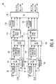
- FIG. 4depicts a block diagram of DCD block 86 .
- DCD block 86performs all of the necessary signal processing functions for two NTSC (analog) television signals.
- DCD block 86includes dual comb filters 90 and 92 for separating luma and chroma from the two incoming analog television signals which are input into respective luma and chroma switches 94 and 96 .
- the respective luma and chroma switches 94 and 96are each clocked at 36 MHz (twice the required frequency of 18 MHz for a single channel) such that each channel's chroma and luma components are switched on every clock. Thus, each 18 MHz channel is processed on every other clock cycle at 36 MHz.
- the chroma componentsare input to respective ACC and chroma demodulation blocks 102 and 109 .
- the UV componentsare meanwhile forwarded to demultiplexers 98 and 100 to obtain respective, separate U and V components.
- the U and V outputs of the chroma demodulation modules 102 and 104(color difference signals) are combined with the U and V outputs of the respective demultiplexers 98 and 100 in respective UV switches 106 and 108 , which again are clocked at 36 MHz (twice the required frequency of 18 MHz for a single channel) such that each channel's chroma and luma components are switched on every clock.
- each 18 MHz channelis processed on every other clock cycle at 36 MHz.
- the luma and UV componentsare forwarded to respective sample rate converters and synchronizing (sync) signal separation blocks 110 and 112 to produce a signal having a standard interface frequency.
- VBIvertical blanking interval
- data slicers 114 and 116wherein closed caption, “v-chip” parental control information, teletext data, program guide information, and the like, is obtained.
- Outputs of the respective sample rate converters and sync processors 110 and 112 , and the respective data slicers 114 and 116are input to video processor 118 to supply the main channel video and second (auxiliary) channel video.
- the second channel videois typically used for PIP or POP.
- undesirable effects of using a single reference clockare compensated for in chroma demodulation sections 102 and 104 , and SRC and sync processors 110 and 112 .
- FIG. 5there is shown a block diagram, generally designated 130 , of the comb filter implementation with dual use of much of the logic circuits of DCD block 86 in accordance with an aspect of the present invention.
- the first composite video of a clocking or sampling frequency of 18 MHzis input into a data storage device 134 holding one line of the video and into a comb filter 132 .
- the second composite video of a clocking or sampling frequency of 18 MHzis input into a data storage device 136 holding one line of the video and into the comb filter 132 .
- Data storage devices 134 and 136are each clocked at the sampling rate of 18 MHz.
- Comb filter 132is clocked at twice 18 MHz or at 36 MHz. In this manner, comb filter 132 alternatively processes the output of data storage devices 134 and 136 .
- DCD block 86combines the two channels, duplicating only the actual data storage components. DCD block 86 also uses the same circuits for most of the processing by operating at twice the required frequency and switching channels on every clock.
Landscapes
- Engineering & Computer Science (AREA)
- Multimedia (AREA)
- Signal Processing (AREA)
- Databases & Information Systems (AREA)
- Television Systems (AREA)
Abstract
Description
This application claims the benefit under 35 U.S.C. § 365 of International Application PCT/US00/28059, filed Oct. 11, 2000, which was published in accordance with PCT Article 21(2) on Apr. 19, 2001 in English; and which claims benefit of U.S. provisional application Ser. No. 60/159,149 filed Oct. 13, 1999.
(1) Field of the Invention
The present invention relates to devices for processing analog and/or digital signals, and more particularly, to integrated circuits that utilize multiple clock frequencies for digitizing and processing various analog and/or digital signals.
(2) Description of the Related Art
Integrated circuits, or ICs, are extensively used in all types of electronic devices. As these electronic devices become more complex, the number of ICs necessary to perform all of the required functions increases and/or the functions of several ICs are combined into a single IC. Even as multiple functions are consolidated into a single IC, it is desirable to reduce the internal complexity of the IC.
Current televisions use many different ICs for processing both analog and digital television signals from various terrestrial and non-terrestrial sources. The next generation of digital/analog televisions, however, will be expected to have even higher levels of integration than current televisions. Higher levels of integration translate into fewer ICs, wherein processes performed by several individual ICs are combined into one IC. However, various obstacles stand in the way of combining processing from analog television signal receivers with those required for digital television signals.
A problem with respect to integration of analog and digital television signal processing ICs is that different sources of video (both analog and digital) may require analog-to-digital (A/D) converters to be run at different sampling rates. Analog television signals are based on line-locked or chroma sub-carrier-locked frequencies, while digitally modulated (digital) television signals are based on their own symbol rates. Also, present A/D technology produces digital crosstalk that adversely affects A/D performance when asynchronous clocks are present.
It is known to use stand-alone digital demodulators using digital interpolation for off-frequency operation. Also, second channel processing for analog signals has been accomplished with an asynchronous sample frequency. In the latter case, however, the main channel is locked to a parameter of the incoming analog television signal, such as horizontal sync pulses or color burst.
The present invention is a single system IC that performs simultaneous digitization and processing of multiple analog and/or digital signals, using a common frequency source that is not locked to a parameter of the incoming signal. Thus, high performance sampling and processing of all incoming signals may be achieved.
The present invention provides for standard analog video decoding for two channels using a single reference frequency (reference clock) that is not locked to either system. That is, the reference clock is not based on, or locked to, a lockable characteristic of either input signal. Two digital signal processors, for satellite and terrestrial television signals, are modified to perform processing based on the same reference frequency. The present invention provides synchronous frequency operation of all A/Ds and digital signal processors of the multiple channels to prevent erroneous sampling and processing of the incoming signal.
In one form of the invention, a single reference clock of a particular frequency is input to a clock generator that generates all of the operational frequencies (clock signals) needed by the A/D converters and decoding circuitry/logic on the IC. The reference clock is independent, e.g., is not locked to, any synchronizing characteristic of the input signals.
Since there is only one reference clock from which all the other sampling and processing frequencies are generated, the A/Ds will be able to operate with high performance, up to 10-bit accuracy, with little to no digital noise. This is generally not possible with asynchronous sampling frequencies because “quiet zones”, needed for sampling the analog input, no longer exist. However, with the multiple sampling frequencies based on a single reference clock (frequency) of the present invention, these quiet zones between digital transitions are preserved.
One circuitry/logic section of the present IC that processes satellite (digital) broadcast television signals, uses an interpolator to process an incoming signal at an appropriate symbol rate related frequency (e.g. 40 MHz) even though the actual samples may be taken at a different frequency (e.g. 54 MHz). A similar procedure is used for terrestrial digital or vestigal sideband (VSB) television signals where twice the symbol rate is an appropriate frequency (e.g. 21.54 MHz) while the sampling frequency (clock signal) is greater than the particular frequency (e.g. 27 MHz). Analog television signal processing is also accomplished at a particular frequency (e.g. 18 MHz) for each channel. Even though the analog television signal samples are not locked to the incoming line rate, the horizontal frequency is determined with sub-sample accuracy for each channel. A final sample rate converter has a frequency (e.g. 27 MHz) that corresponds to a frequency for luma (e.g. 13.5 MHz) plus a frequency for each of the color difference signals (e.g. 6.75 MHz). This provides non-jittering lines of data output. Additionally, a chroma demodulator of the present IC uses a digital discrete-time oscillator (DTO) that is locked to the incoming chroma burst signal for each of the incoming signals. Thus, all of the digital processing is achieved using synchronous clocks in spite of the asynchronous character inherent in the various processing sections of circuitry/logic, such as by four types of television signal systems.
The present invention also achieves dual use of much of the digital circuitry in the dual NTSC signal processing section. The digital color decoder (DCD) performs all of the necessary signal processing functions for decoding NTSC video including comb filtering for separating luma and chroma, chroma demodulation for generating the color difference signals, synchronizing (sync) signal separation, sample rate conversion (SRC) to a standard interface frequency, and vertical blanking interval (VBI) data slicing. The VBI typically includes closed caption, “V-chip” parental control/rating information, program guide, teletext data, and the like. All of these functions are included for both the main channel video and the second channel video, which is usually used for picture-in-picture (PIP).
In accordance with another aspect of the present invention, the DCD combines the two channels, duplicating only the actual data storage components required for the two channels, and uses the same circuits for most of the processing by running at twice the required sampling/clock frequency and switching channels on every clock cycle. Thus, for example, each 18 MHz channel is processed on every other clock cycle at 36 MHz.
In another form, the present invention includes an analog signal processing section and a clock generator. The analog signal processing section is operable to process analog signals having a synchronizing component, such as a horizontal sync pulse or the like. The clock generator is operable to produce internal clocking signals based on an external reference signal for use by the analog signal processing section, wherein the external reference signal is independent of the synchronizing component of the analog signals.
In another form, the present invention includes an analog signal processing section, a digital signal processing section, a first A/D converter associated with the analog signal processing section, and a second A/D converter associated with the digital signal processing section. The integrated circuit further includes a clock generator operable to provide first and second clock signals for the first and second analog-to-digital converters respectively from a single reference clock signal, wherein the first and second clock signals provide synchronous operation of the first and second analog-to-digital converters.
In yet another form, the present invention includes an analog signal processing section, a digital signal processing section, and a clock generator. The clock generator is operable to produce multiple clock signals of different frequencies for use by the analog and digital processing sections, wherein the clock generator uses a single reference clock signal of a given frequency that is independent of any synchronizing characteristic of the input analog and/or digital signal. The analog and digital signal processing sections process their respective analog and digital signals simultaneously.
The present invention is described with reference to the accompanying drawings, wherein:
Corresponding reference characters indicate corresponding parts throughout the several views.
With reference toFIG. 1 there is depicted a block diagram of asystem 10 suitable for using an IC according to the present invention.System 10 comprises a plurality of integrated circuits (ICs) for signal and/or data and information processing, wherein at least one IC requires multiple clocks, clock frequencies, or clock/clocking signals for proper functioning. This type of IC may be termed a multiple clock IC. It should be appreciated thatsystem 10 is an exemplary environment/application utilizing the present multiple clock IC. The multiple clock IC ofsystem 10, in accordance with the principles set forth herein, may take many forms and/or perform many functions as is known to those skilled in the art.
Insystem 10, the multiple clock IC performs television signal processing for a variety of television signal formats from a variety of sources. Briefly, the multiple clock television signal processor IC incorporating the present invention is adapted/operable to process digital satellite television signals, terrestrial (including cable distribution) digital television signals, and terrestrial (including cable distribution) analog television signals. These analog and digital signals may be provided in various encoding schemes and/or modulation schemes.
Processing circuit/logic 16 is also operable, to process analog audio and video television signals (“analog television signals”) fromterrestrial analog antenna 30 received via a signal path orline 32, as well as analog television signals from CATV (cable television)system 34. The modulation/encoding format of the analog television signals is typically NTSC, but other formats may be used. The processing of analog television signals typically includes digitizing the input signals through appropriate circuitry, software, and/or other components. Digital television signals fromCATV system 34 may also be decoded and processed. It should be appreciated thattelevision apparatus 12 is adapted to receive and process analog and/or digital television signals from sources other than that shown.
Televisionsignal processing device 12 also typically includesmemory 18, which includes stored program instructions (i.e. software) for controlling the operation of televisionsignal processing device 12. Circuitry/logic 24 is provided for other functionality of televisionsignal processing device 12, which functionality is not necessary for understanding or practicing the present invention, and will not be described in detail.
Televisionsignal processing device 12 may be an analog/digital television including, but not limited to DTV-320 HDTV (High Definition Television) manufactured by Thomson Consumer Electronics, Inc. of Indianapolis, Ind., a digital television such as a high definition digital television (HDTV), a set-top box capable of utilizing analog/digital television signals, a television signal storage device, or any other device that can process various forms of television signals.
In accordance with an aspect of the present invention, at least one of the plurality of ICs insystem 10 is a multiple clock IC. The multiple clock IC utilized in processing circuitry/logic 16 oftelevision apparatus 12, is known as a Universal Link IC, and is illustrated inFIG. 2 . Universal linkIC 40 is an integrated circuit of mixed signal design, i.e. it has both analog and digital television signal processing circuitry, and incorporates, or integrates, several television signal processing functions into a single IC.
Referring toFIG. 2 , there is shown a block diagram of Universal LinkUniversal Link IC 40 used intelevision apparatus 12. The multiple clock signals of different frequencies are generated byUniversal Link IC 40 using a single externally generated reference clock signal of a given frequency.Universal Link IC 40 includes I/O pin 48 that receives the externally generated reference clock signal. In the present embodiment,Universal Link IC 40 uses an externally provided 27 MHz reference clock signal. Other external reference clock signal frequencies may be used in accordance with the principles set forth herein.
Notably, the external reference clock signal is not based on, or locked to, any lockable characteristic, such as a sync pulse or color burst, of an incoming television signal (either analog or digital). Rather, the external reference clock signal is chosen to provide easy multiplication and division thereof for generating clock signals of appropriate frequencies to accommodate the clocking signal frequency requirements of the various sections or blocks of circuitry/logic ofUniversal Link IC 40.
InUniversal Link IC 40, the external reference clock signal is provided to Phase Locked Loop (PLL)synthesizer 50, which produces an output clock signal of a given frequency on output/line 52. Here, the PLL output clock signal is chosen to be 108 MHz and may be considered an internal reference clock signal. All remaining required clock signals are generated from this internal reference clock signal.
The 108 MHz internal reference clock signal is provided toclock generator 54, which contains the appropriate circuitry/logic to generate multiple clock frequencies. The actual number of clock signals produced byclock generator 54 is dependent upon the clock signal requirements of the particular IC. InUniversal Link IC 40,clock generator 54 produces four (4) clock signals of different frequencies and one (1) clock signal of the same frequency as the internal reference clock signal. Each generated clock signal is then routed to the appropriate section or block of circuitry/logic.
In accordance with the present invention, the internal IC reference clock frequency generated byPLL clock synthesizer 50 is a multiple of the external reference clock frequency. More particularly, the internal IC reference clock frequency is preferably a whole number multiple of the external reference clock frequency. The internal IC reference clock frequency is also chosen such that it can be divided into the plurality of IC clock signals or frequencies that are usable by the various sections or blocks of circuitry/logic.
In the present case, the internal reference clock signal frequency is 108 MHz, which is four (4) times the external reference clock signal frequency of 27 MHz.Clock generator 54 then produces a 54 MHz clock signal, which is one-half (½) of the 108 MHz internal IC clock signal, a 36 MHz clock signal, which is one-third (⅓) of the 108 MHz internal IC clock signal, a 27 MHz clock signal which is one-fourth (¼) of the 108 MHz internal IC clock signal and an 18 MHz clock signal which is one-sixth (⅙) of the 108 MHz internal IC clock signal. Therefore,clock generator 54 generates 4 subclocks that are subharmonics of the master internal clock with no phase shift.
Another factor in determining the frequencies of internal clock signals is the sampling rates, or the clocking rates, for the various sections or blocks of circuitry/logic ofUniversal Link IC 40. As indicated above,Universal Link IC 40 includes three main sections. The three main sections are: “Satlink”section 42, which is operable to receive and demodulate/decode satellite transmitted television signals; “VSB (Vestigal SideBand) link”section 44 which is operable to receive and demodulate/decode terrestrially transmitted general digital and/or digital high definition (HDTV) signals; and “DCD” (Digital Color Decoder)section 46, which is a block of circuitry/logic that is operable to provide switching, chroma demodulation, and other signal processing of NTSC (analog) signals.Universal Link IC 40 provides several separate decoding/demodulation systems, including a first system for a main analog television signal, a second system for an auxiliary analog television signal (such as PIP or picture-in-picture and/or POP or picture-on-picture), a third system for digital satellite television signals, and a fourth system for digital terrestrial television signals.Sections
Similar toSatlink section 42,VSB section 44 receives the VSB digital broadcast television signal through an appropriate “x-bit” A/D converter.VSB section 44 receives the VSB signal through 10-bit A/D converter 62 that is clocked with the 27 MHz clock signal.Demodulation block 64,equalizer block 66,phase tracker block 68, and Forward Error Correction (FEC) block70 further process the terrestrial broadcast digital television signal. In particular,demodulation block 64,equalizer block 66,phase tracker block 68, and FEC block70 processes the VSB signal at twice a symbol rate related frequency for the VSB (i.e. terrestrial) broadcast digital television signals. In the present case, the appropriate symbol rate frequency is 10.77 MHz, so twice the appropriate symbol rate frequency is 21.54 MHz. The 10-bit A/D converter 62, however, utilizes the 27 MHz IC clock signal to clock or sample (oversample) the incoming television signal, even though it requires only a 21.54 MHz clock or sampling signal. The 27 MHz clock provides an approximately twenty-five percent (25%) increase in clock or sampling frequency over the sampling frequency required.
InDCD section 46, the analog sampling is accomplished using the 18 MHz clock signal for each channel of the analog television signal. Even though these samples are not locked to a characteristic of the input television signal, this horizontal frequency is determined with sub-sample accuracy for each channel.DCD section 46 is operable to receive two analog television signals (i.e. one for the main channel and the other for the PIP or POP) at DCDanalog circuits section 72. The four (4) CV/Y signals thereof are input intoswitch 74 that appropriately sends the signals to two 10-bit A/D converters switch 80 that appropriately sends the signal to two 10-bit A/D converters D converters digital color decoder 86. The final sample rate convertion is accomplished at 27 MHz (sequential 13.5 MHz for luma and 6.75 MHz for each of the color difference signals. This provides non-jittering lines of data output. In addition, the chroma demodulator uses a digital discrete time oscillator (DTO) that is locked to the incoming chroma burst signal for each of the incoming signals.
All of the A/D processing and digital signal processing is accomplished using synchronous clocks in spite of the asynchronous character inherent in these four signaling systems. Also, each IC clock signal frequency generated byclock generator 54 is equal to or greater than the clock/sampling signal frequency required for proper operation of the appropriate portion of the circuitry/logic. Such oversampling may be accommodated for later in the processing of the particular signal. Undesirable effects generated by the synchronous operation of the A/Ds and signal processor sections may be compensated for by thechroma demodulation sections synch processors
Since there is only one reference clock signal from which all of the other sampling and processing frequencies are generated, the A/Ds will be able to operate with high performance (i.e. up to 10-bit accuracy) and have little to no digital noise. This not possible with asynchronous sampling frequencies because the “quiet zones” needed for sampling the analog signal no longer exist. However, with multiple sampling frequencies based on the same clock, the quiet zones between digital transitions are preserved. (seeFIG. 3 ).
Another aspect of the present invention is the dual use of portions of the digital circuitry for processing NTSC television signals. In this regard, reference is made toFIG. 4 , which depicts a block diagram ofDCD block 86.DCD block 86 performs all of the necessary signal processing functions for two NTSC (analog) television signals.DCD block 86 includes dual comb filters90 and92 for separating luma and chroma from the two incoming analog television signals which are input into respective luma and chroma switches94 and96. The respective luma and chroma switches94 and96 are each clocked at 36 MHz (twice the required frequency of 18 MHz for a single channel) such that each channel's chroma and luma components are switched on every clock. Thus, each 18 MHz channel is processed on every other clock cycle at 36 MHz.
The chroma components are input to respective ACC and chroma demodulation blocks102 and109. The UV components are meanwhile forwarded to demultiplexers98 and100 to obtain respective, separate U and V components. The U and V outputs of thechroma demodulation modules 102 and104 (color difference signals) are combined with the U and V outputs of therespective demultiplexers
The luma and UV components are forwarded to respective sample rate converters and synchronizing (sync) signal separation blocks110 and112 to produce a signal having a standard interface frequency. Additionally, vertical blanking interval (VBI) data slicing is accomplished bydata slicers sync processors video processor 118 to supply the main channel video and second (auxiliary) channel video. The second channel video is typically used for PIP or POP. As noted earlier, undesirable effects of using a single reference clock are compensated for inchroma demodulation sections sync processors
With reference toFIG. 5 , there is shown a block diagram, generally designated130, of the comb filter implementation with dual use of much of the logic circuits ofDCD block 86 in accordance with an aspect of the present invention. The first composite video of a clocking or sampling frequency of 18 MHz is input into adata storage device 134 holding one line of the video and into acomb filter 132. At the same time, the second composite video of a clocking or sampling frequency of 18 MHz is input into adata storage device 136 holding one line of the video and into thecomb filter 132.Data storage devices Comb filter 132 is clocked at twice 18 MHz or at 36 MHz. In this manner,comb filter 132 alternatively processes the output ofdata storage devices
Thus, instead of two completely different circuits,DCD block 86 combines the two channels, duplicating only the actual data storage components.DCD block 86 also uses the same circuits for most of the processing by operating at twice the required frequency and switching channels on every clock.
While this invention has been described as having a preferred design and/or configuration, the present invention can be further modified within the spirit and scope of this disclosure. This application is therefore intended to cover such departures from the present disclosure as come within known or customary practice in the art to which this invention pertains and which fall within the limits of the appended claims. In particular, the present invention is applicable to other circuits where there are prerequisites to operate systems with different frequency requirements, where it is desired to operate the systems/circuits on the same silicon space, especially those with A/Ds and other analog circuits, in addition to the digital circuitry/logic.
Claims (7)
1. A signal processing apparatus, comprising:
first and second signal inputs for receiving first and second input signals having respective synchronizing characteristics;
a first clock generator for generating a reference clock signal, the reference clock signal being independent of the synchronizing characteristics of the first and second input signals;
a second clock generator, coupled to the first clock generator, for producing a plurality of further clock signals in response to the reference clock signal; and
a signal processing section, coupled to the first and second signal inputs and the second clock generator, for sampling and processing the first and second input signals in accordance with a sampling rate and an appropriate signal standard, the signal processing section having a plurality of analog to digital (A/D) converters that are clocked by respective ones of the plurality of further clock signals,
the A/D converters being clocked by respective ones of the plurality of further clock signals, which are independent of the synchronizing characteristics of the first and second input signals and have a frequency substantially equal to the sampling rate, wherein the signal processing section processes the first and second input signals using a single processing channel, the single processing channel being clocked by a further clock signal that has a signal frequency of at least twice the required clocking speed necessary for processing a single one of the first and second input signals.
2. The signal processing apparatus ofclaim 1 , wherein the first and second input signals are television signals.
3. The signal processing apparatus ofclaim 1 , wherein the signal processing section is further operable to process a digital input signal having a synchronizing characteristic, and the reference clock signal is independent of the synchronizing characteristic of the digital input signal.
4. A television apparatus, comprising:
first and second signal inputs for receiving first and second television signals having respective synchronizing characteristics;
a first clock signal generator for producing a reference clock signal that is independent of the synchronizing characteristics of the first and second television signals;
a second clock signal generator, coupled to the first clock signal generator, for producing a plurality of further clock signals in response to the reference clock signal;
a signal processor, coupled to the signal inputs and the second clock signal generator, for sampling and processing the first and second television signals in accordance with appropriate signal standards and providing output signals suitable for display on a display device, the signal processor including a plurality of analog to digital (A/D) converters coupled to the second clock signal generator; and
an signal output, coupled to the signal processor, for receiving and coupling the output signals to a display device,
the A/D converters of the signal processor being clocked by respective ones of the plurality of further clock signals, which are independent of the synchronizing characteristics of the input signals, and have a frequency substantially equal to the sampling rate, wherein
the signal processing section decodes the first and second television signals using a single processing channel, and the single processing channel is clocked by a clock signal that has frequency of at least twice the required clocking speed necessary for processing a single one of the television signals.
5. A method for processing input signals having synchronizing components, the method comprising the steps of:
receiving first and second input signals having respective synchronizing components;
generating a reference clock signal, the reference clock signal being independent of the synchronizing characteristics of the first and second input signals;
generating a plurality of further clock signals based on the reference clock signal;
converting the first and second input signals into corresponding first and second digital signals using analog to digital (A/D) converters that are clocked using one of the plurality of further clock signals; and
decoding the converted digital signals in accordance with appropriate television signal standards using decoding circuitry/logic to provide output signals suitable for display, the decoding circuitry/logic being clocked by at least one of the plurality of further clock signals, wherein the decoding is performed using a single processing channel that is clocked by an internal clock signal that has a frequency of at least twice the required clocking speed necessary for processing a single input signal
the A/D converters being clocked by respective ones of the plurality of further clock signals, which are independent of the synchronizing characteristic of the input signal and having a frequency substantially equal to the sampling rate.
6. The method according toclaim 5 , wherein
the receiving step further comprises receiving a digital input signal having a synchronizing characteristic, and
the decoding step further comprises decoding the digital input signal using decoding circuitry/logic that is clocked by a respective one of the internal clock signals that is independent of the synchronizing characteristic of the digital input signal.
7. The method according toclaim 5 , wherein
the receiving step comprises receiving an analog television signal.
Priority Applications (1)
| Application Number | Priority Date | Filing Date | Title |
|---|---|---|---|
| US10/089,904US7102692B1 (en) | 1999-10-13 | 2000-10-11 | Digital and analog television signal digitization and processing device |
Applications Claiming Priority (3)
| Application Number | Priority Date | Filing Date | Title |
|---|---|---|---|
| US15914999P | 1999-10-13 | 1999-10-13 | |
| US10/089,904US7102692B1 (en) | 1999-10-13 | 2000-10-11 | Digital and analog television signal digitization and processing device |
| PCT/US2000/028059WO2001028255A1 (en) | 1999-10-13 | 2000-10-11 | Digital and analog television signal digitization and processing device |
Publications (1)
| Publication Number | Publication Date |
|---|---|
| US7102692B1true US7102692B1 (en) | 2006-09-05 |
Family
ID=36939489
Family Applications (1)
| Application Number | Title | Priority Date | Filing Date |
|---|---|---|---|
| US10/089,904Expired - LifetimeUS7102692B1 (en) | 1999-10-13 | 2000-10-11 | Digital and analog television signal digitization and processing device |
Country Status (1)
| Country | Link |
|---|---|
| US (1) | US7102692B1 (en) |
Cited By (36)
| Publication number | Priority date | Publication date | Assignee | Title |
|---|---|---|---|---|
| US20050066374A1 (en)* | 2003-09-19 | 2005-03-24 | Funai Electric Co., Ltd. | Receiving apparatus and television set equipped with the same |
| US20050129145A1 (en)* | 2003-12-12 | 2005-06-16 | Lg Electronics Inc. | E8-VSB reception system |
| US20050179822A1 (en)* | 2001-10-16 | 2005-08-18 | Hiroshi Takano | Method and apparatus for automatically switching between analog and digital input signals |
| US20050212970A1 (en)* | 2004-03-26 | 2005-09-29 | Joskin Yves R | Video frame grabber apparatus and method |
| US20050259746A1 (en)* | 2004-05-21 | 2005-11-24 | Texas Instruments Incorporated | Clocked output of multiple data streams from a common data port |
| US20050265127A1 (en)* | 2003-05-13 | 2005-12-01 | International Business Machines Corporation | Real time clock circuit having an internal clock generator |
| US20050276548A1 (en)* | 2004-06-10 | 2005-12-15 | Jiang Fu | Transcoding closed captioning data from broadcast DTV onto DVD |
| US20060078054A1 (en)* | 2004-10-13 | 2006-04-13 | Cirrus Logic, Inc. | Method and apparatus to improve decoding of composite video signals |
| US20060120243A1 (en)* | 2002-07-04 | 2006-06-08 | Tadashi Kurita | Reproduction device and content information reproduction method |
| US7365796B1 (en)* | 2003-05-20 | 2008-04-29 | Pixelworks, Inc. | System and method for video signal decoding using digital signal processing |
| US7391472B1 (en) | 2003-05-20 | 2008-06-24 | Pixelworks, Inc. | System and method for adaptive color burst phase correction |
| US7420625B1 (en) | 2003-05-20 | 2008-09-02 | Pixelworks, Inc. | Fuzzy logic based adaptive Y/C separation system and method |
| US20080240297A1 (en)* | 2007-03-26 | 2008-10-02 | Lg Electronics Inc. | Digital broadcasting system and method of processing data |
| US20090028079A1 (en)* | 2007-06-26 | 2009-01-29 | Lg Electronics Inc. | Digital broadcast system for transmitting/receiving digital broadcast data, and data processing method for use in the same |
| US20090052587A1 (en)* | 2007-08-24 | 2009-02-26 | Lg Electronics Inc. | Digital broadcasting system and method of processing data in digital broadcasting system |
| US20090060051A1 (en)* | 2007-06-26 | 2009-03-05 | Lg Electronics Inc. | Digital broadcasting system and data processing method |
| US20090060030A1 (en)* | 2007-08-24 | 2009-03-05 | Lg Electronics Inc. | Digital broadcasting system and method of processing data in digital broadcasting system |
| US7532254B1 (en) | 2003-05-20 | 2009-05-12 | Pixelworks, Inc. | Comb filter system and method |
| US20090125940A1 (en)* | 2007-04-06 | 2009-05-14 | Lg Electronics Inc. | Method for controlling electronic program information and apparatus for receiving the electronic program information |
| US7605867B1 (en)* | 2003-05-20 | 2009-10-20 | Pixelworks, Inc. | Method and apparatus for correction of time base errors |
| US7701512B1 (en) | 2003-05-20 | 2010-04-20 | Pixelworks, Inc. | System and method for improved horizontal and vertical sync pulse detection and processing |
| US7739581B2 (en) | 2006-04-29 | 2010-06-15 | Lg Electronics, Inc. | DTV transmitting system and method of processing broadcast data |
| US7804860B2 (en) | 2005-10-05 | 2010-09-28 | Lg Electronics Inc. | Method of processing traffic information and digital broadcast system |
| US7822134B2 (en) | 2007-03-30 | 2010-10-26 | Lg Electronics, Inc. | Digital broadcasting system and method of processing data |
| US7831885B2 (en) | 2007-07-04 | 2010-11-09 | Lg Electronics Inc. | Digital broadcast receiver and method of processing data in digital broadcast receiver |
| US7840868B2 (en) | 2005-10-05 | 2010-11-23 | Lg Electronics Inc. | Method of processing traffic information and digital broadcast system |
| US7873104B2 (en) | 2006-10-12 | 2011-01-18 | Lg Electronics Inc. | Digital television transmitting system and receiving system and method of processing broadcasting data |
| US7876835B2 (en) | 2006-02-10 | 2011-01-25 | Lg Electronics Inc. | Channel equalizer and method of processing broadcast signal in DTV receiving system |
| US7940855B2 (en) | 2007-03-26 | 2011-05-10 | Lg Electronics Inc. | DTV receiving system and method of processing DTV signal |
| US8005167B2 (en) | 2007-08-24 | 2011-08-23 | Lg Electronics Inc. | Digital broadcasting system and method of processing data in digital broadcasting system |
| US8099654B2 (en) | 2007-08-24 | 2012-01-17 | Lg Electronics Inc. | Digital broadcasting system and method of processing data in the digital broadcasting system |
| US8218092B1 (en) | 2008-03-03 | 2012-07-10 | Csr Technology Inc. | Apparatus for receiving both analog and digital TV signals |
| US8351497B2 (en) | 2006-05-23 | 2013-01-08 | Lg Electronics Inc. | Digital television transmitting system and receiving system and method of processing broadcast data |
| US8370728B2 (en) | 2007-07-28 | 2013-02-05 | Lg Electronics Inc. | Digital broadcasting system and method of processing data in digital broadcasting system |
| US8433973B2 (en) | 2007-07-04 | 2013-04-30 | Lg Electronics Inc. | Digital broadcasting system and method of processing data |
| WO2022164579A1 (en)* | 2021-01-28 | 2022-08-04 | SEAKR Engineering, Inc. | System and method for measuring small frequency differences |
Citations (11)
| Publication number | Priority date | Publication date | Assignee | Title |
|---|---|---|---|---|
| US4138741A (en)* | 1976-03-19 | 1979-02-06 | Rca Corporation | Disc eccentricity compensating system |
| US5367337A (en) | 1992-04-30 | 1994-11-22 | Image Data Corporation | Method and apparatus for capturing video images |
| US5537113A (en)* | 1992-06-17 | 1996-07-16 | Advantest Corp. | A/D or D/A conversion using distribution of differential waveforms to interleaved converters |
| US5745468A (en)* | 1995-01-11 | 1998-04-28 | Olympus Optical Co., Ltd. | Mark edge recorded signal reproducing device for use in optical disk apparatus |
| US5808691A (en) | 1995-12-12 | 1998-09-15 | Cirrus Logic, Inc. | Digital carrier synthesis synchronized to a reference signal that is asynchronous with respect to a digital sampling clock |
| US5812608A (en)* | 1995-05-05 | 1998-09-22 | Nokia Technology Gmbh | Method and circuit arrangement for processing received signal |
| WO1998046027A1 (en) | 1997-04-09 | 1998-10-15 | Koninklijke Philips Electronics N.V. | Color decoding |
| WO1999046931A1 (en) | 1998-03-09 | 1999-09-16 | General Instrument Corporation | Digital signal processor for multistandard television reception |
| US6014366A (en)* | 1996-04-15 | 2000-01-11 | Nec Corporation | Variable-bandwidth frequency division multiplex communication system |
| US6141057A (en)* | 1993-07-26 | 2000-10-31 | Pixel Instruments Corp. | Apparatus and method for maintaining synchronization of multiple delayed signals of differing types |
| US6160508A (en)* | 1997-12-29 | 2000-12-12 | Telefonaktiebolaget Lm Ericsson | Method and device for analogue to digital conversion |
- 2000
- 2000-10-11USUS10/089,904patent/US7102692B1/ennot_activeExpired - Lifetime
Patent Citations (11)
| Publication number | Priority date | Publication date | Assignee | Title |
|---|---|---|---|---|
| US4138741A (en)* | 1976-03-19 | 1979-02-06 | Rca Corporation | Disc eccentricity compensating system |
| US5367337A (en) | 1992-04-30 | 1994-11-22 | Image Data Corporation | Method and apparatus for capturing video images |
| US5537113A (en)* | 1992-06-17 | 1996-07-16 | Advantest Corp. | A/D or D/A conversion using distribution of differential waveforms to interleaved converters |
| US6141057A (en)* | 1993-07-26 | 2000-10-31 | Pixel Instruments Corp. | Apparatus and method for maintaining synchronization of multiple delayed signals of differing types |
| US5745468A (en)* | 1995-01-11 | 1998-04-28 | Olympus Optical Co., Ltd. | Mark edge recorded signal reproducing device for use in optical disk apparatus |
| US5812608A (en)* | 1995-05-05 | 1998-09-22 | Nokia Technology Gmbh | Method and circuit arrangement for processing received signal |
| US5808691A (en) | 1995-12-12 | 1998-09-15 | Cirrus Logic, Inc. | Digital carrier synthesis synchronized to a reference signal that is asynchronous with respect to a digital sampling clock |
| US6014366A (en)* | 1996-04-15 | 2000-01-11 | Nec Corporation | Variable-bandwidth frequency division multiplex communication system |
| WO1998046027A1 (en) | 1997-04-09 | 1998-10-15 | Koninklijke Philips Electronics N.V. | Color decoding |
| US6160508A (en)* | 1997-12-29 | 2000-12-12 | Telefonaktiebolaget Lm Ericsson | Method and device for analogue to digital conversion |
| WO1999046931A1 (en) | 1998-03-09 | 1999-09-16 | General Instrument Corporation | Digital signal processor for multistandard television reception |
Cited By (120)
| Publication number | Priority date | Publication date | Assignee | Title |
|---|---|---|---|---|
| US20050179822A1 (en)* | 2001-10-16 | 2005-08-18 | Hiroshi Takano | Method and apparatus for automatically switching between analog and digital input signals |
| US7414674B2 (en)* | 2001-10-16 | 2008-08-19 | Sony Corporation | Method and apparatus for automatically switching between analog and digital input signals |
| US20060120243A1 (en)* | 2002-07-04 | 2006-06-08 | Tadashi Kurita | Reproduction device and content information reproduction method |
| US7558462B2 (en)* | 2002-07-04 | 2009-07-07 | Sony Corporation | Reproduction device and content information reproduction method |
| US7661008B2 (en)* | 2003-05-13 | 2010-02-09 | International Business Machines Corporation | Real time clock circuit having an internal clock generator |
| US20050265127A1 (en)* | 2003-05-13 | 2005-12-01 | International Business Machines Corporation | Real time clock circuit having an internal clock generator |
| US7646436B1 (en) | 2003-05-20 | 2010-01-12 | Pixelworks, Inc. | Fuzzy logic based adaptive Y/C separation system and method |
| US7532254B1 (en) | 2003-05-20 | 2009-05-12 | Pixelworks, Inc. | Comb filter system and method |
| US7605867B1 (en)* | 2003-05-20 | 2009-10-20 | Pixelworks, Inc. | Method and apparatus for correction of time base errors |
| US7701512B1 (en) | 2003-05-20 | 2010-04-20 | Pixelworks, Inc. | System and method for improved horizontal and vertical sync pulse detection and processing |
| US7365796B1 (en)* | 2003-05-20 | 2008-04-29 | Pixelworks, Inc. | System and method for video signal decoding using digital signal processing |
| US7391472B1 (en) | 2003-05-20 | 2008-06-24 | Pixelworks, Inc. | System and method for adaptive color burst phase correction |
| US7420625B1 (en) | 2003-05-20 | 2008-09-02 | Pixelworks, Inc. | Fuzzy logic based adaptive Y/C separation system and method |
| US20050066374A1 (en)* | 2003-09-19 | 2005-03-24 | Funai Electric Co., Ltd. | Receiving apparatus and television set equipped with the same |
| US7545444B2 (en)* | 2003-09-19 | 2009-06-09 | Funai Electric Co., Ltd. | Receiving apparatus and television set for receiving broadcast signals |
| US7555066B2 (en)* | 2003-12-12 | 2009-06-30 | Lg Electronics Inc. | E8-VSB reception system |
| US20050129145A1 (en)* | 2003-12-12 | 2005-06-16 | Lg Electronics Inc. | E8-VSB reception system |
| US20050212970A1 (en)* | 2004-03-26 | 2005-09-29 | Joskin Yves R | Video frame grabber apparatus and method |
| US7570305B2 (en)* | 2004-03-26 | 2009-08-04 | Euresys S.A. | Sampling of video data and analyses of the sampled data to determine video properties |
| US20050259746A1 (en)* | 2004-05-21 | 2005-11-24 | Texas Instruments Incorporated | Clocked output of multiple data streams from a common data port |
| US8306128B2 (en)* | 2004-05-21 | 2012-11-06 | Texas Instruments Incorporated | Clocked output of multiple data streams from a common data port |
| US20050276548A1 (en)* | 2004-06-10 | 2005-12-15 | Jiang Fu | Transcoding closed captioning data from broadcast DTV onto DVD |
| US20060078054A1 (en)* | 2004-10-13 | 2006-04-13 | Cirrus Logic, Inc. | Method and apparatus to improve decoding of composite video signals |
| US7339628B2 (en)* | 2004-10-13 | 2008-03-04 | Cirrus Logic, Inc. | Method and apparatus to improve decoding of composite video signals |
| US7742110B1 (en) | 2005-07-22 | 2010-06-22 | Pixelworks, Inc. | Comb filter system and method |
| USRE48627E1 (en) | 2005-10-05 | 2021-07-06 | Lg Electronics Inc. | Method of processing traffic information and digital broadcast system |
| US8098694B2 (en) | 2005-10-05 | 2012-01-17 | Lg Electronics Inc. | Method of processing traffic information and digital broadcast system |
| USRE49757E1 (en) | 2005-10-05 | 2023-12-12 | Lg Electronics Inc. | Method of processing traffic information and digital broadcast system |
| USRE47294E1 (en) | 2005-10-05 | 2019-03-12 | Lg Electronics Inc. | Method of processing traffic information and digital broadcast system |
| US8018977B2 (en) | 2005-10-05 | 2011-09-13 | Lg Electronics Inc. | Method of processing traffic information and digital broadcast system |
| US8018978B2 (en) | 2005-10-05 | 2011-09-13 | Lg Electronics Inc. | Method of processing traffic information and digital broadcast system |
| USRE46891E1 (en) | 2005-10-05 | 2018-06-12 | Lg Electronics Inc. | Method of processing traffic information and digital broadcast system |
| US8473807B2 (en) | 2005-10-05 | 2013-06-25 | Lg Electronics Inc. | Method of processing traffic information and digital broadcast system |
| US7804860B2 (en) | 2005-10-05 | 2010-09-28 | Lg Electronics Inc. | Method of processing traffic information and digital broadcast system |
| US8018976B2 (en) | 2005-10-05 | 2011-09-13 | Lg Electronics Inc. | Method of processing traffic information and digital broadcast system |
| US8542709B2 (en) | 2005-10-05 | 2013-09-24 | Lg Electronics Inc. | Method of processing traffic information and digital broadcast system |
| US7840868B2 (en) | 2005-10-05 | 2010-11-23 | Lg Electronics Inc. | Method of processing traffic information and digital broadcast system |
| US8526508B2 (en) | 2006-02-10 | 2013-09-03 | Lg Electronics Inc. | Channel equalizer and method of processing broadcast signal in DTV receiving system |
| US7876835B2 (en) | 2006-02-10 | 2011-01-25 | Lg Electronics Inc. | Channel equalizer and method of processing broadcast signal in DTV receiving system |
| US8204137B2 (en) | 2006-02-10 | 2012-06-19 | Lg Electronics Inc. | Channel equalizer and method of processing broadcast signal in DTV receiving system |
| US8054891B2 (en) | 2006-02-10 | 2011-11-08 | Lg Electronics Inc. | Channel equalizer and method of processing broadcast signal in DTV receiving system |
| US8355451B2 (en) | 2006-02-10 | 2013-01-15 | Lg Electronics Inc. | Channel equalizer and method of processing broadcast signal in DTV receiving system |
| US9185413B2 (en) | 2006-02-10 | 2015-11-10 | Lg Electronics Inc. | Channel equalizer and method of processing broadcast signal in DTV receiving system |
| US10277255B2 (en) | 2006-02-10 | 2019-04-30 | Lg Electronics Inc. | Channel equalizer and method of processing broadcast signal in DTV receiving system |
| US8689086B2 (en) | 2006-04-29 | 2014-04-01 | Lg Electronics Inc. | DTV transmitting system and method of processing broadcast data |
| US9680506B2 (en) | 2006-04-29 | 2017-06-13 | Lg Electronics Inc. | DTV transmitting system and method of processing broadcast data |
| US7739581B2 (en) | 2006-04-29 | 2010-06-15 | Lg Electronics, Inc. | DTV transmitting system and method of processing broadcast data |
| US8984381B2 (en) | 2006-04-29 | 2015-03-17 | LG Electronics Inc. LLP | DTV transmitting system and method of processing broadcast data |
| US8429504B2 (en) | 2006-04-29 | 2013-04-23 | Lg Electronics Inc. | DTV transmitting system and method of processing broadcast data |
| US9425827B2 (en) | 2006-04-29 | 2016-08-23 | Lg Electronics Inc. | DTV transmitting system and method of processing broadcast data |
| US20100223528A1 (en)* | 2006-04-29 | 2010-09-02 | Hyoung Gon Lee | Dtv transmitting system and method of processing broadcast data |
| US9178536B2 (en) | 2006-04-29 | 2015-11-03 | Lg Electronics Inc. | DTV transmitting system and method of processing broadcast data |
| US9564989B2 (en) | 2006-05-23 | 2017-02-07 | Lg Electronics Inc. | Digital television transmitting system and receiving system and method of processing broadcast data |
| US8804817B2 (en) | 2006-05-23 | 2014-08-12 | Lg Electronics Inc. | Digital television transmitting system and receiving system and method of processing broadcast data |
| US8351497B2 (en) | 2006-05-23 | 2013-01-08 | Lg Electronics Inc. | Digital television transmitting system and receiving system and method of processing broadcast data |
| US10057009B2 (en) | 2006-05-23 | 2018-08-21 | Lg Electronics Inc. | Digital television transmitting system and receiving system and method of processing broadcast data |
| US8611731B2 (en) | 2006-10-12 | 2013-12-17 | Lg Electronics Inc. | Digital television transmitting system and receiving system and method of processing broadcast data |
| US7873104B2 (en) | 2006-10-12 | 2011-01-18 | Lg Electronics Inc. | Digital television transmitting system and receiving system and method of processing broadcasting data |
| US9831986B2 (en) | 2006-10-12 | 2017-11-28 | Lg Electronics Inc. | Digital television transmitting system and receiving system and method of processing broadcasting data |
| US10454616B2 (en) | 2006-10-12 | 2019-10-22 | Lg Electronics Inc. | Digital television transmitting system and receiving system and method of processing broadcasting data |
| US9392281B2 (en) | 2006-10-12 | 2016-07-12 | Lg Electronics Inc. | Digital television transmitting system and receiving system and method of processing broadcasting data |
| US8223884B2 (en) | 2007-03-26 | 2012-07-17 | Lg Electronics Inc. | DTV transmitting system and method of processing DTV signal |
| US8068561B2 (en) | 2007-03-26 | 2011-11-29 | Lg Electronics Inc. | DTV receiving system and method of processing DTV signal |
| US8218675B2 (en) | 2007-03-26 | 2012-07-10 | Lg Electronics Inc. | Digital broadcasting system and method of processing |
| US20080240297A1 (en)* | 2007-03-26 | 2008-10-02 | Lg Electronics Inc. | Digital broadcasting system and method of processing data |
| US10244274B2 (en) | 2007-03-26 | 2019-03-26 | Lg Electronics Inc. | DTV receiving system and method of processing DTV signal |
| US8731100B2 (en) | 2007-03-26 | 2014-05-20 | Lg Electronics Inc. | DTV receiving system and method of processing DTV signal |
| US10070160B2 (en) | 2007-03-26 | 2018-09-04 | Lg Electronics Inc. | DTV receiving system and method of processing DTV signal |
| US7940855B2 (en) | 2007-03-26 | 2011-05-10 | Lg Electronics Inc. | DTV receiving system and method of processing DTV signal |
| US9924206B2 (en) | 2007-03-26 | 2018-03-20 | Lg Electronics Inc. | DTV receiving system and method of processing DTV signal |
| US9912354B2 (en) | 2007-03-26 | 2018-03-06 | Lg Electronics Inc. | Digital broadcasting system and method of processing data |
| US9198005B2 (en) | 2007-03-26 | 2015-11-24 | Lg Electronics Inc. | Digital broadcasting system and method of processing data |
| US8023047B2 (en) | 2007-03-26 | 2011-09-20 | Lg Electronics Inc. | Digital broadcasting system and method of processing data |
| US9736508B2 (en) | 2007-03-26 | 2017-08-15 | Lg Electronics Inc. | DTV receiving system and method of processing DTV signal |
| US8488717B2 (en) | 2007-03-26 | 2013-07-16 | Lg Electronics Inc. | Digital broadcasting system and method of processing data |
| US7881408B2 (en) | 2007-03-26 | 2011-02-01 | Lg Electronics Inc. | Digital broadcasting system and method of processing data |
| US7822134B2 (en) | 2007-03-30 | 2010-10-26 | Lg Electronics, Inc. | Digital broadcasting system and method of processing data |
| US9521441B2 (en) | 2007-03-30 | 2016-12-13 | Lg Electronics Inc. | Digital broadcasting system and method of processing data |
| US8532222B2 (en) | 2007-03-30 | 2013-09-10 | Lg Electronics Inc. | Digital broadcasting system and method of processing data |
| US8213544B2 (en) | 2007-03-30 | 2012-07-03 | Lg Electronics Inc. | Digital broadcasting system and method of processing data |
| US8276177B2 (en) | 2007-04-06 | 2012-09-25 | Lg Electronics Inc. | Method for controlling electronic program information and apparatus for receiving the electronic program information |
| US20090125940A1 (en)* | 2007-04-06 | 2009-05-14 | Lg Electronics Inc. | Method for controlling electronic program information and apparatus for receiving the electronic program information |
| US9860016B2 (en) | 2007-06-26 | 2018-01-02 | Lg Electronics Inc. | Digital broadcast system for transmitting/receiving digital broadcast data, and data processing method for use in the same |
| US10097312B2 (en) | 2007-06-26 | 2018-10-09 | Lg Electronics Inc. | Digital broadcast system for transmitting/receiving digital broadcast data, and data processing method for use in the same |
| US20090028079A1 (en)* | 2007-06-26 | 2009-01-29 | Lg Electronics Inc. | Digital broadcast system for transmitting/receiving digital broadcast data, and data processing method for use in the same |
| US20090060051A1 (en)* | 2007-06-26 | 2009-03-05 | Lg Electronics Inc. | Digital broadcasting system and data processing method |
| US8374252B2 (en) | 2007-06-26 | 2013-02-12 | Lg Electronics Inc. | Digital broadcasting system and data processing method |
| USRE46728E1 (en) | 2007-06-26 | 2018-02-20 | Lg Electronics Inc. | Digital broadcasting system and data processing method |
| US8135038B2 (en) | 2007-06-26 | 2012-03-13 | Lg Electronics Inc. | Digital broadcast system for transmitting/receiving digital broadcast data, and data processing method for use in the same |
| US8135034B2 (en) | 2007-06-26 | 2012-03-13 | Lg Electronics Inc. | Digital broadcast system for transmitting/receiving digital broadcast data, and data processing method for use in the same |
| US8670463B2 (en) | 2007-06-26 | 2014-03-11 | Lg Electronics Inc. | Digital broadcast system for transmitting/receiving digital broadcast data, and data processing method for use in the same |
| US9490936B2 (en) | 2007-06-26 | 2016-11-08 | Lg Electronics Inc. | Digital broadcast system for transmitting/receiving digital broadcast data, and data processing method for use in the same |
| US7953157B2 (en) | 2007-06-26 | 2011-05-31 | Lg Electronics Inc. | Digital broadcasting system and data processing method |
| US8201050B2 (en) | 2007-07-04 | 2012-06-12 | Lg Electronics Inc. | Broadcast transmitting system and method of processing broadcast data in the broadcast transmitting system |
| US9444579B2 (en) | 2007-07-04 | 2016-09-13 | Lg Electronics Inc. | Broadcast transmitter and method of processing broadcast service data for transmission |
| US8042019B2 (en) | 2007-07-04 | 2011-10-18 | Lg Electronics Inc. | Broadcast transmitting/receiving system and method of processing broadcast data in a broadcast transmitting/receiving system |
| US9184770B2 (en) | 2007-07-04 | 2015-11-10 | Lg Electronics Inc. | Broadcast transmitter and method of processing broadcast service data for transmission |
| US8954829B2 (en) | 2007-07-04 | 2015-02-10 | Lg Electronics Inc. | Digital broadcasting system and method of processing data |
| US9660764B2 (en) | 2007-07-04 | 2017-05-23 | Lg Electronics Inc. | Broadcast transmitter and method of processing broadcast service data for transmission |
| US7831885B2 (en) | 2007-07-04 | 2010-11-09 | Lg Electronics Inc. | Digital broadcast receiver and method of processing data in digital broadcast receiver |
| US9094159B2 (en) | 2007-07-04 | 2015-07-28 | Lg Electronics Inc. | Broadcasting transmitting system and method of processing broadcast data in the broadcast transmitting system |
| US8433973B2 (en) | 2007-07-04 | 2013-04-30 | Lg Electronics Inc. | Digital broadcasting system and method of processing data |
| US8370728B2 (en) | 2007-07-28 | 2013-02-05 | Lg Electronics Inc. | Digital broadcasting system and method of processing data in digital broadcasting system |
| US8391404B2 (en) | 2007-08-24 | 2013-03-05 | Lg Electronics Inc. | Digital broadcasting system and method of processing data in digital broadcasting system |
| US20090060030A1 (en)* | 2007-08-24 | 2009-03-05 | Lg Electronics Inc. | Digital broadcasting system and method of processing data in digital broadcasting system |
| US8099654B2 (en) | 2007-08-24 | 2012-01-17 | Lg Electronics Inc. | Digital broadcasting system and method of processing data in the digital broadcasting system |
| US9755849B2 (en) | 2007-08-24 | 2017-09-05 | Lg Electronics Inc. | Digital broadcasting system and method of processing data in digital broadcasting system |
| US7646828B2 (en) | 2007-08-24 | 2010-01-12 | Lg Electronics, Inc. | Digital broadcasting system and method of processing data in digital broadcasting system |
| US8370707B2 (en) | 2007-08-24 | 2013-02-05 | Lg Electronics Inc. | Digital broadcasting system and method of processing data in the digital broadcasting system |
| US8165244B2 (en) | 2007-08-24 | 2012-04-24 | Lg Electronics Inc. | Digital broadcasting system and method of processing data in digital broadcasting system |
| US7965778B2 (en) | 2007-08-24 | 2011-06-21 | Lg Electronics Inc. | Digital broadcasting system and method of processing data in digital broadcasting system |
| USRE47183E1 (en) | 2007-08-24 | 2018-12-25 | Lg Electronics Inc. | Digital broadcasting system and method of processing data in digital broadcasting system |
| US8005167B2 (en) | 2007-08-24 | 2011-08-23 | Lg Electronics Inc. | Digital broadcasting system and method of processing data in digital broadcasting system |
| US8335280B2 (en) | 2007-08-24 | 2012-12-18 | Lg Electronics Inc. | Digital broadcasting system and method of processing data in digital broadcasting system |
| US9369154B2 (en) | 2007-08-24 | 2016-06-14 | Lg Electronics Inc. | Digital broadcasting system and method of processing data in digital broadcasting system |
| US20090052587A1 (en)* | 2007-08-24 | 2009-02-26 | Lg Electronics Inc. | Digital broadcasting system and method of processing data in digital broadcasting system |
| US8964856B2 (en) | 2007-08-24 | 2015-02-24 | Lg Electronics Inc. | Digital broadcasting system and method of processing data in digital broadcasting system |
| US8218092B1 (en) | 2008-03-03 | 2012-07-10 | Csr Technology Inc. | Apparatus for receiving both analog and digital TV signals |
| WO2022164579A1 (en)* | 2021-01-28 | 2022-08-04 | SEAKR Engineering, Inc. | System and method for measuring small frequency differences |
| US12200093B2 (en) | 2021-01-28 | 2025-01-14 | Seakr Engineering, Llc | System and method for measuring small frequency differences |
Similar Documents
| Publication | Publication Date | Title |
|---|---|---|
| US7102692B1 (en) | Digital and analog television signal digitization and processing device | |
| US6441860B1 (en) | Video signal processing apparatus | |
| US6147713A (en) | Digital signal processor for multistandard television reception | |
| KR100426889B1 (en) | A self-moving image scanning format converter with seamless switching | |
| KR100426890B1 (en) | A video scan format converter suitable for high-definition television systems | |
| EP0928539B1 (en) | Television with integrated receiver decoder | |
| JPH02237280A (en) | Standard/high definition television receiver | |
| KR920000580B1 (en) | Digital receiver | |
| EP0793363A2 (en) | Timing recovery system for a digital signal processor | |
| KR0153618B1 (en) | Apparatus for processing bpsk signals transmitted with ntsc tv on quadrature phase video carrier | |
| EP1221262B1 (en) | Parallel digitizing and processing of plural analogue television signals | |
| KR100574703B1 (en) | Apparatus and Method for Providing Video Lip Sync Delay | |
| US5194937A (en) | Television signal converting apparatus and method | |
| JP2003018614A (en) | Picture signal processor | |
| US7583802B2 (en) | Method for using a synchronous sampling design in a fixed-rate sampling mode | |
| JP2914268B2 (en) | Video signal processing apparatus and processing method thereof | |
| Lerner | Digital TV: makers bet on VLSI | |
| Brett et al. | High performance picture-in-picture (PIP) IC using embedded DRAM technology | |
| KR20000044160A (en) | Timing recovery circuit of digital television receiving system | |
| JPH0638181A (en) | Television receiver | |
| HK1021464B (en) | Television with integrated receiver decoder | |
| JPH0470176A (en) | television format converter | |
| MXPA00008840A (en) | Digital signal processor for multistandard television reception | |
| JPH09233498A (en) | Signal processor |
Legal Events
| Date | Code | Title | Description |
|---|---|---|---|
| AS | Assignment | Owner name:THOMSON LICENSING S.A., FRANCE Free format text:ASSIGNMENT OF ASSIGNORS INTEREST;ASSIGNORS:CARLSGAARD, ERIC STEPHEN;RUMREICH, MARK FRANCIS;STEWART, JOHN SIDNEY;REEL/FRAME:012965/0528 Effective date:20001017 | |
| AS | Assignment | Owner name:THOMSON LICENSING, FRANCE Free format text:ASSIGNMENT OF ASSIGNORS INTEREST;ASSIGNOR:THOMSON LICENSING S.A.;REEL/FRAME:017955/0949 Effective date:20060718 | |
| STCF | Information on status: patent grant | Free format text:PATENTED CASE | |
| FPAY | Fee payment | Year of fee payment:4 | |
| FPAY | Fee payment | Year of fee payment:8 | |
| MAFP | Maintenance fee payment | Free format text:PAYMENT OF MAINTENANCE FEE, 12TH YEAR, LARGE ENTITY (ORIGINAL EVENT CODE: M1553) Year of fee payment:12 | |
| AS | Assignment | Owner name:MAGNOLIA LICENSING LLC, TEXAS Free format text:ASSIGNMENT OF ASSIGNORS INTEREST;ASSIGNOR:THOMSON LICENSING S.A.S.;REEL/FRAME:053570/0237 Effective date:20200708 |