US7102375B2 - Pin electronics with high voltage functionality - Google Patents
Pin electronics with high voltage functionalityDownload PDFInfo
- Publication number
- US7102375B2 US7102375B2US11/023,023US2302304AUS7102375B2US 7102375 B2US7102375 B2US 7102375B2US 2302304 AUS2302304 AUS 2302304AUS 7102375 B2US7102375 B2US 7102375B2
- Authority
- US
- United States
- Prior art keywords
- pin
- amplifier
- mode
- driver
- voltage
- Prior art date
- Legal status (The legal status is an assumption and is not a legal conclusion. Google has not performed a legal analysis and makes no representation as to the accuracy of the status listed.)
- Expired - Lifetime
Links
- 238000012360testing methodMethods0.000claimsabstractdescription61
- 238000000034methodMethods0.000claimsdescription18
- 230000007246mechanismEffects0.000claimsdescription16
- 238000010998test methodMethods0.000claimsdescription2
- 239000004020conductorSubstances0.000description13
- 230000008569processEffects0.000description13
- 230000004044responseEffects0.000description12
- 239000004065semiconductorSubstances0.000description8
- 238000004590computer programMethods0.000description7
- 230000006870functionEffects0.000description7
- 230000007704transitionEffects0.000description5
- 238000010586diagramMethods0.000description4
- 238000005259measurementMethods0.000description3
- 238000004891communicationMethods0.000description2
- 238000012545processingMethods0.000description2
- 238000004458analytical methodMethods0.000description1
- 238000013459approachMethods0.000description1
- 230000000712assemblyEffects0.000description1
- 238000000429assemblyMethods0.000description1
- 230000002457bidirectional effectEffects0.000description1
- 230000005540biological transmissionEffects0.000description1
- 238000012512characterization methodMethods0.000description1
- 238000013461designMethods0.000description1
- 230000000644propagated effectEffects0.000description1
Images


Classifications
- G—PHYSICS
- G01—MEASURING; TESTING
- G01R—MEASURING ELECTRIC VARIABLES; MEASURING MAGNETIC VARIABLES
- G01R31/00—Arrangements for testing electric properties; Arrangements for locating electric faults; Arrangements for electrical testing characterised by what is being tested not provided for elsewhere
- G01R31/26—Testing of individual semiconductor devices
- G—PHYSICS
- G01—MEASURING; TESTING
- G01R—MEASURING ELECTRIC VARIABLES; MEASURING MAGNETIC VARIABLES
- G01R31/00—Arrangements for testing electric properties; Arrangements for locating electric faults; Arrangements for electrical testing characterised by what is being tested not provided for elsewhere
- G01R31/28—Testing of electronic circuits, e.g. by signal tracer
- G01R31/2832—Specific tests of electronic circuits not provided for elsewhere
- G01R31/2836—Fault-finding or characterising
- G01R31/2844—Fault-finding or characterising using test interfaces, e.g. adapters, test boxes, switches, PIN drivers
- H—ELECTRICITY
- H01—ELECTRIC ELEMENTS
- H01L—SEMICONDUCTOR DEVICES NOT COVERED BY CLASS H10
- H01L22/00—Testing or measuring during manufacture or treatment; Reliability measurements, i.e. testing of parts without further processing to modify the parts as such; Structural arrangements therefor
Definitions
- This patent applicationrelates generally to testing a device and, more particularly, to pin electronics.
- ATEAutomatic test equipment
- DUTdevice-under-test
- the inventionis an integrated circuit (IC) for use in testing a device.
- the ICincludes a pin electronics (PE) driver having an output, a pin and a buffer connected to the output of the PE driver and the pin.
- the first voltage measured at the pinis greater than a second voltage measured at the output.
- PEpin electronics
- the inventionis automatic test equipment (ATE) for use with a device under test.
- the automatic test equipmentincludes an integrated circuit (IC).
- the ICincludes a pin electronics (PE) driver having an output having a second voltage, a high voltage pin having a first voltage being greater than the second voltage and a buffer connected to the output of the PE driver and the high voltage pin.
- PEpin electronics
- the bufferincludes a first amplifier having an input connected to a voltage source.
- the voltage sourcecorresponds to the terminal voltage used by the PE driver.
- the gain of the first amplifierhas a gain greater than one.
- the bufferincludes a second amplifier having an input connected to the output of the PE driver.
- the second amplifierhas a gain of about one.
- the bufferincludes a switching mechanism configured to establish, in a first mode, a first electrical connection between the first amplifier and the pin, and, in a second mode, to establish a second electrical connection between the second amplifier and the pin.
- the first mode and the second modeare mutually exclusive.
- the pin electronics driveris tri-stated and includes an enable input signal and the switching mechanism includes an input signal to establish the first mode or the second mode.
- the input signal of the switching mechanism and the enable input signalare the same.
- the switching mechanismcomprises a first switch and a second switch.
- the inventionis a method of testing a device.
- the methodincludes connecting an output of a pin electronics driver to a buffer, connecting the buffer to a pin and providing a first voltage at the pin greater than a second voltage at the output of the PE driver.
- the bufferincludes a first amplifier having a gain of one and including an input connected to the output of the PE driver and a second amplifier having a gain greater than one and including an input connected to a voltage source.
- the methodmay include receiving a signal indicating a first mode or a second mode; in the first mode, establishing a first electrical connection between the first amplifier and the pin; and in the second mode, establishing a second electrical connection between the second amplifier and the pin.
- the first mode and the second modemay be mutually exclusive.
- HVhigh voltage
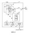
- FIG. 1is a diagrammatic view of a system for testing devices.
- FIG. 2is a diagrammatic view of a tester.
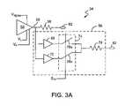
- FIG. 3Ais an integrated circuit diagram for providing a high voltage function using pin electronics (PE) in a first mode.
- PEpin electronics
- FIG. 3Bis an integrated circuit diagram for providing a high voltage function using pin electronics (PE) in a second mode.
- PEpin electronics
- FIG. 4Ais a flowchart showing a process for implementing a high voltage function using pin electronics.
- FIG. 4Bis a flowchart showing a process for deactivating a high voltage function.
- FIG. 5Ais an integrated circuit diagram with a tri-state PE driver with the high voltage functionality enabled.
- FIG. 5Bis an integrated circuit diagram with a tri-state PE driver with the high voltage functionality disabled.
- a system 10 for testing a device-under-test (DUT) 18such as semiconductor devices includes a tester 12 such as automatic test equipment (ATE) or other similar testing device.
- tester 12such as automatic test equipment (ATE) or other similar testing device.
- system 10includes a computer system 14 that interfaces with tester 12 over a hardwire connection 16 .
- computer system 14sends commands to tester 12 that initiate the execution of routines and functions for testing DUT 18 .
- Such executing test routinesmay initiate the generation and transmission of test signals to the DUT 18 and collecting responses from the DUT.
- DUTsmay be semiconductor devices such as an integrated circuit (IC) chip (e.g., memory chip, microprocessor, analog-to-digital converter, digital-to-analog converter, etc.).
- ICintegrated circuit
- tester 12is connected to one or more connector pins that provide an interface for the internal circuitry of DUT 18 .
- DUTse.g., as many as sixty-four or one hundred twenty-eight connector pins (or more) may be interfaced to tester 12 .
- semiconductor device tester 12is connected to one connector pin of DUT 18 by a hardwire connection.
- a conductor 20e.g., cable
- test signalse.g., PMU test signals, PE test signals, etc.
- Conductor 20also senses signals at pin 22 in response to the test signals provided by semiconductor device tester 12 .
- a voltage signal or a current signalmay be sensed at pin 22 in response to a test signal and sent over conductor 20 to tester 12 for analysis.
- Such single port testsmay also be performed on other pins included in DUT 18 .
- tester 12may provide test signals into other pins and collect associated signals reflected back over conductors (that deliver the provided signals). By collecting the reflected signals, the input impedance of the pins may be characterized along with other single port testing quantities.
- a digital signalmay be sent over conductor 20 to pin 22 for storing a digital value on DUT 18 . Once stored, DUT 18 may be accessed to retrieve and send the stored digital value over conductor 20 to tester 12 . The retrieved digital value may then be identified to determine if the proper value was stored on DUT 18 .
- a two-port testmay also be performed by semiconductor device tester 12 .
- a test signalmay be injected over conductor 20 into pin 22 and a response signal may be collected from one or more other pins of DUT 18 .
- This response signalis provided to semiconductor device tester 12 to determine such quantities as gain response, phase response, and other throughput measurement quantities.
- semiconductor device tester 12includes an interface card 24 that can communicate with numerous pins.
- interface card 24may transmit test signals to, e.g., 32, 64, or 128 pins and collect the corresponding responses.
- Each communication link to a pinis typically referred to as a channel and by providing test signals to a large number of channels, testing time is reduced since multiple tests may be simultaneously performed.
- the overall number of channelsincreases, thereby further reducing testing time.
- two additional interface cards 26 and 28are shown to demonstrate that multiple interface cards may populate tester 12 .
- Each interface cardincludes a dedicated integrated circuit (IC) chip (e.g., an application specific integrated circuit (ASIC)) for performing particular test functions.
- ICintegrated circuit
- interface card 24includes IC chip 30 for performing parametric measurement unit (PMU) tests and Pin electronics (PE) tests.
- IC chip 30respectively has a PMU stage 32 that includes circuitry for performing PMU tests and a PE stage 34 that includes circuitry for performing PE tests.
- interface cards 26 and 28respectively include IC chips 36 and 38 that include PMU and PE circuitry.
- PMU testinginvolves providing a DC voltage or current signal to the DUT to determine such quantities as input and output impedance, current leakage, and other types of DC performance characterizations.
- PE testinginvolves sending AC test signals and waveforms to a DUT (e.g., DUT 18 ) and collecting responses to further characterize the performance of the DUT.
- IC chip 30may transmit (to the DUT) AC test signals that represent a vector of binary values for storing on the DUT. Once stored, the DUT is accessed by tester 12 to determine if the correct binary values have been stored. Since digital signals typically include abrupt voltage transitions, the circuitry in PE stage 34 on IC chip 30 operates at a relatively high speed in comparison to the circuitry in PMU stage 32 .
- a conducting trace 40connects IC chip 30 to an interface board connector 42 that allows signals to be passed on and off interface board 24 .
- Interface board connector 42is also connected to a conductor 44 that is connected to an interface connector 46 that allows signals to be passed to and from tester 12 .
- conductor 20is connected to interface connector 46 for bidirectional signal passing between tester 12 and pin 22 of DUT 18 .
- an interface devicemay be used to connect one or more conductors from tester 12 to the DUT.
- the DUTe.g., DUT 18
- the DUTmay be mounted onto a device interface board (DIB) for providing easy access to each DUT pin.
- conductor 20may be connected to the DIB for placing test signals on the appropriate pin(s) (e.g., pin 22 ) of the DUT.
- conducting trace 40 and conductor 44respectively connect IC chip 30 and interface board 24 for delivering and collecting signals.
- IC chip 30(along with IC chips 36 and 38 ) typically has multiple pins (e.g., eight, sixteen, etc.) that are respectively connected with multiple conducting traces and corresponding conductors for providing and collecting signals from the DUT (via a DIB).
- tester 12may connect to two or more DIB's for interfacing the channels provided by interface cards 24 , 26 , and 28 to one or multiple devices under test.
- tester 12To initiate and control the testing performed by interface cards 24 , 26 , and 28 , tester 12 includes PMU control circuitry 48 and PE control circuitry 50 that provide test parameters (e.g., test signal voltage level, test signal current level, digital values, etc.) for producing test signals and analyzing DUT responses. Tester 12 also includes a computer interface 52 that allows computer system 14 to control the operations executed by tester 12 and also allows data (e.g., test parameters, DUT responses, etc.) passing between tester 12 and computer system 14 .
- test parameterse.g., test signal voltage level, test signal current level, digital values, etc.
- tester 12also includes a computer interface 52 that allows computer system 14 to control the operations executed by tester 12 and also allows data (e.g., test parameters, DUT responses, etc.) passing between tester 12 and computer system 14 .
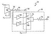
- pin electronics 34includes a pin electronics (PE) driver 54 having an output 55 , a buffer 56 connected to the output 55 of the PE driver 54 , a matched resistor 58 connected to the output of the PE driver, a test pin 62 connected to the matched resistor 58 and a high voltage pin 82 connected to the buffer 56 .
- PE driver 54receives input signals, which control the operation of the PE driver, for example, a voltage low (V L ), a voltage high (V H ) and a termination voltage (V TERM ).
- V Lvoltage low
- V Hvoltage high
- V TERMtermination voltage
- the PE circuitrymay be used to generate high voltages at the high voltage pin 82 .
- the term “high voltage”means a voltage that is a higher voltage than what is provided at the output 55 of the PE driver 54 .
- Buffer 56includes a first amplifier 66 , a second amplifier 70 , and a switching mechanism 74 , which includes a switch 76 a and a switch 76 b and a matched resistor 78 .
- An input of amplifier 66is connected to V TERM and an output of amplifier 66 is connected to switch 76 a .
- V TERMBy using an already existing voltage source with the pin electronics such as V TERM , a new voltage source does not need to be added.
- An input of amplifier 70is connected to the output 55 of PE driver 54 and an output of amplifier 70 is connected to switch 76 b.
- amplifier 66has a gain of about 2.33
- amplifier 70has a gain of 1
- matched resistor 78is about 50 ohms.
- the voltage at the output 55 of the PE driver 54ranges from 0 to 6 volts.
- V TERMranges from 0 to 6 volts and the voltage at the high voltage pin 82 ranges from 0 to 14 volts.
- switch mechanism 74In a first mode ( FIG. 3A ), switch mechanism 74 includes switch 76 a in an open circuit and switch 76 b in a closed circuit. When activated by an input signal, S IN , switch mechanism 74 transitions into a second mode ( FIG. 3B ).
- the second modeincludes switch 76 a in a closed circuit and switch 76 b in an open circuit.
- the input signal, S INmay also transition switch mechanism 74 transitions from the second mode to the first mode.
- switch 76 a and switch 76 bmove simultaneously so that neither switch 76 a nor switch 76 b is in a closed position at the same moment.
- switch mechanism 74is either in the first mode or the second mode.
- FIG. 4Ais a flowchart showing a process 100 for implementing high voltage functionality using software to select a high voltage by transitioning from the first mode to the second mode.
- Process 100receives ( 104 ) an input to switch the high voltage pin 82 to a high voltage.
- Process 100connects ( 108 ) amplifier 66 to HV pin by closing switch 76 a .
- Process 100disconnects ( 112 ) PE driver 54 from HV voltage pin 82 by opening switch 76 b.
- FIG. 4Amay be modified to transition from the second mode to the first mode by performing the opposite actions in block 108 and 112 .
- process 200receives ( 204 ) an input to remove the high voltage from the high voltage pin 82 .
- Process 200disconnects ( 208 ) amplifier 66 from HV pin 82 by opening switch 76 a .
- Process 200connects ( 212 ) PE driver 54 to HV voltage pin 82 by closing switch 76 b.
- PE driver 54may be tri-stated to prevent driver 54 from outputting current and/or voltage.
- a tri-state circuitsuch as driver 54
- a tri-state circuitis similar to an ordinary circuit, except that it has an additional input 90 called the “enable” input.
- the enable inputis “0”
- the tri-state circuitbehaves like a corresponding normal (non-tri-state) circuit.
- the enable inputis “1”
- the output of the tri-state circuitin this case, driver 54
- driver 54when driver 54 is tri-stated, its output is disconnected from resistor 58 and buffer 56 , preventing driver 54 from supplying current and/or voltage to pin 62 and pin 82 .
- the signal S INmay be tied to the input 90 .
- PE driver 54When the input 90 is “1”, PE driver 54 is “off,” switch 76 a is “closed” and switch 76 b is “open” (see FIG. 5A ).
- the enable inputis “0”, PE driver is “on,” switch 76 b is “closed” and switch 76 a is “open” (See FIG. 5B ).
- the tester described hereinis not limited to use with the hardware and software described above.
- the testercan be implemented in digital electronic circuitry, or in computer hardware, firmware, software, or in combinations thereof.
- the testercan be implemented, at least in part, via a computer program product, i.e., a computer program tangibly embodied in an information carrier, e.g., in a machine-readable storage device or in a propagated signal, for execution by, or to control the operation of, data processing apparatus, e.g., a programmable processor, a computer, or multiple computers.
- a computer programcan be written in any form of programming language, including compiled or interpreted languages, and it can be deployed in any form, including as a stand-alone program or as a module, component, subroutine, or other unit suitable for use in a computing environment.
- a computer programcan be deployed to be executed on one computer or on multiple computers at one site or distributed across multiple sites and interconnected by a communication network.
- Method steps associated with implementing the testercan be performed by one or more programmable processors executing one or more computer programs to perform the functions of the tester. All or part of the tester can be implemented as, special purpose logic circuitry, e.g., an FPGA (field programmable gate array) and/or an ASIC (application-specific integrated circuit).
- special purpose logic circuitrye.g., an FPGA (field programmable gate array) and/or an ASIC (application-specific integrated circuit).
- processors suitable for the execution of a computer programinclude, by way of example, both general and special purpose microprocessors, and any one or more processors of any kind of digital computer.
- a processorwill receive instructions and data from a read-only memory or a random access memory or both.
- Elements of a computerinclude a processor for executing instructions and one or more memory devices for storing instructions and data.
- Processes 100 and 200are not limited to the specific embodiments described herein.
- processes 100 and 200are not limited to the specific processing order of FIGS. 4A and 4B .
- the blocks of FIGS. 4A and 4Bmay be re-ordered or removed, as necessary, to achieve the results set forth above.
- blocks 108 and 112 in process 100 and blocks 212 and 208 in process 200may be reordered or performed simultaneously.
- circuitryis not limited to the specific examples described herein.
- this disclosuredescribes circuitry within automatic test equipment, the circuitry described herein may be used in any circuit environment requiring high voltage pins providing voltages higher than provided by a pin electronics driver.
- amplifier 66may be supplied by another voltage source on IC chip 30 than V TERM .
Landscapes
- Engineering & Computer Science (AREA)
- Physics & Mathematics (AREA)
- General Physics & Mathematics (AREA)
- General Engineering & Computer Science (AREA)
- Manufacturing & Machinery (AREA)
- Computer Hardware Design (AREA)
- Microelectronics & Electronic Packaging (AREA)
- Power Engineering (AREA)
- Tests Of Electronic Circuits (AREA)
Abstract
Description
Claims (13)
Priority Applications (6)
| Application Number | Priority Date | Filing Date | Title |
|---|---|---|---|
| US11/023,023US7102375B2 (en) | 2004-12-23 | 2004-12-23 | Pin electronics with high voltage functionality |
| EP05854966AEP1849018A4 (en) | 2004-12-23 | 2005-12-16 | Pin electronics with high voltage functionality |
| CN2005800440104ACN101084444B (en) | 2004-12-23 | 2005-12-16 | Pin Electronics with High Voltage Capabilities |
| PCT/US2005/046332WO2006071668A2 (en) | 2004-12-23 | 2005-12-16 | Pin electronics with high voltage functionality |
| JP2007548428AJP4698680B2 (en) | 2004-12-23 | 2005-12-16 | Pin electronics with high voltage capability |
| KR1020077013818AKR100905507B1 (en) | 2004-12-23 | 2005-12-16 | Pin electronics with high voltage functionality |
Applications Claiming Priority (1)
| Application Number | Priority Date | Filing Date | Title |
|---|---|---|---|
| US11/023,023US7102375B2 (en) | 2004-12-23 | 2004-12-23 | Pin electronics with high voltage functionality |
Publications (2)
| Publication Number | Publication Date |
|---|---|
| US20060139048A1 US20060139048A1 (en) | 2006-06-29 |
| US7102375B2true US7102375B2 (en) | 2006-09-05 |
Family
ID=36610716
Family Applications (1)
| Application Number | Title | Priority Date | Filing Date |
|---|---|---|---|
| US11/023,023Expired - LifetimeUS7102375B2 (en) | 2004-12-23 | 2004-12-23 | Pin electronics with high voltage functionality |
Country Status (6)
| Country | Link |
|---|---|
| US (1) | US7102375B2 (en) |
| EP (1) | EP1849018A4 (en) |
| JP (1) | JP4698680B2 (en) |
| KR (1) | KR100905507B1 (en) |
| CN (1) | CN101084444B (en) |
| WO (1) | WO2006071668A2 (en) |
Cited By (7)
| Publication number | Priority date | Publication date | Assignee | Title |
|---|---|---|---|---|
| US20070069755A1 (en)* | 2005-09-28 | 2007-03-29 | Sartschev Ronald A | Pin electronics driver |
| US20080104461A1 (en)* | 2006-10-30 | 2008-05-01 | Ajay Khoche | ATE architecture and method for DFT oriented testing |
| US20090322369A1 (en)* | 2008-06-30 | 2009-12-31 | Samsung Electronics Co., Ltd. | Test system |
| US20120319718A1 (en)* | 2011-06-14 | 2012-12-20 | Samsung Electronics Co., Ltd. | Signal transmission apparatus and semiconductor test apparatus using the same |
| US11125817B2 (en) | 2019-10-14 | 2021-09-21 | Analog Devices, Inc. | Compound pin driver |
| US11264906B2 (en) | 2019-12-13 | 2022-03-01 | Analog Devices, Inc. | Compound pin driver controller |
| US20220236325A1 (en)* | 2019-04-16 | 2022-07-28 | Celerint, Llc | Device interface board compliance testing using impedance response profiling |
Families Citing this family (2)
| Publication number | Priority date | Publication date | Assignee | Title |
|---|---|---|---|---|
| US10976367B2 (en)* | 2018-12-13 | 2021-04-13 | Micron Technology, Inc. | Controller structural testing with automated test vectors |
| KR102856918B1 (en)* | 2020-03-31 | 2025-09-09 | 에스케이하이닉스 주식회사 | Semiconductor Test System |
Citations (14)
| Publication number | Priority date | Publication date | Assignee | Title |
|---|---|---|---|---|
| US5101153A (en) | 1991-01-09 | 1992-03-31 | National Semiconductor Corporation | Pin electronics test circuit for IC device testing |
| US5200696A (en) | 1990-09-10 | 1993-04-06 | Ltx Corporation | Test system apparatus with Schottky diodes with programmable voltages |
| US5514976A (en) | 1994-02-03 | 1996-05-07 | Mitsubishi Denki Kabushiki Kaisha | Semiconductor test apparatus having improved current load circuit |
| US5521493A (en) | 1994-11-21 | 1996-05-28 | Megatest Corporation | Semiconductor test system including a novel driver/load circuit |
| US5617035A (en) | 1993-11-01 | 1997-04-01 | Motorola, Inc. | Method for testing integrated devices |
| US6498473B1 (en) | 1999-10-01 | 2002-12-24 | Advantest Corporation | Pin electronics having current measuring unit and testing apparatus having pin electronics thereof |
| US6677775B2 (en) | 2001-01-10 | 2004-01-13 | Analog Devices, Inc. | Circuit testing device using a driver to perform electronics testing |
| US6687868B1 (en)* | 1999-04-06 | 2004-02-03 | Advantest Corporation | Test device and method for electrically testing electronic device |
| US6828775B2 (en) | 2003-02-21 | 2004-12-07 | Semtech Corporation | High-impedance mode for precision measurement unit |
| US6836136B2 (en) | 2002-12-18 | 2004-12-28 | Teradyne, Inc. | Pin driver for AC and DC semiconductor device testing |
| US6859902B1 (en)* | 2000-10-02 | 2005-02-22 | Credence Systems Corporation | Method and apparatus for high speed IC test interface |
| US6879175B2 (en) | 2003-03-31 | 2005-04-12 | Teradyne, Inc. | Hybrid AC/DC-coupled channel for automatic test equipment |
| US6885213B2 (en) | 2002-09-13 | 2005-04-26 | Logicvision, Inc. | Circuit and method for accurately applying a voltage to a node of an integrated circuit |
| US20050189950A1 (en) | 2004-02-27 | 2005-09-01 | Broadcom Corporation | ATE measurement technique for comparator threshold voltage |
Family Cites Families (11)
| Publication number | Priority date | Publication date | Assignee | Title |
|---|---|---|---|---|
| JPH0650787Y2 (en)* | 1987-10-28 | 1994-12-21 | 株式会社アドバンテスト | Input/output circuit for IC testing |
| US4998026A (en)* | 1989-04-19 | 1991-03-05 | Hewlett-Packard Company | Driver circuit for in-circuit overdrive/functional tester |
| JPH03255377A (en)* | 1990-03-05 | 1991-11-14 | Nec Corp | Testing apparatus of integrated circuit |
| JP3457091B2 (en)* | 1995-03-17 | 2003-10-14 | アジレント・テクノロジー株式会社 | Voltage-current characteristic measuring device |
| JPH09325176A (en)* | 1996-06-05 | 1997-12-16 | Advantest Corp | Ic tester |
| US5844913A (en)* | 1997-04-04 | 1998-12-01 | Hewlett-Packard Company | Current mode interface circuitry for an IC test device |
| US6049901A (en)* | 1997-09-16 | 2000-04-11 | Stock; Mary C. | Test system for integrated circuits using a single memory for both the parallel and scan modes of testing |
| JPH11326441A (en)* | 1998-05-20 | 1999-11-26 | Advantest Corp | Semiconductor testing device |
| JP2001183431A (en)* | 1999-04-06 | 2001-07-06 | Advantest Corp | Test apparatus and test method |
| US6694462B1 (en)* | 2000-08-09 | 2004-02-17 | Teradyne, Inc. | Capturing and evaluating high speed data streams |
| US6940271B2 (en) | 2001-08-17 | 2005-09-06 | Nptest, Inc. | Pin electronics interface circuit |
- 2004
- 2004-12-23USUS11/023,023patent/US7102375B2/ennot_activeExpired - Lifetime
- 2005
- 2005-12-16KRKR1020077013818Apatent/KR100905507B1/enactiveActive
- 2005-12-16WOPCT/US2005/046332patent/WO2006071668A2/enactiveSearch and Examination
- 2005-12-16JPJP2007548428Apatent/JP4698680B2/enactiveActive
- 2005-12-16EPEP05854966Apatent/EP1849018A4/ennot_activeWithdrawn
- 2005-12-16CNCN2005800440104Apatent/CN101084444B/enactiveActive
Patent Citations (14)
| Publication number | Priority date | Publication date | Assignee | Title |
|---|---|---|---|---|
| US5200696A (en) | 1990-09-10 | 1993-04-06 | Ltx Corporation | Test system apparatus with Schottky diodes with programmable voltages |
| US5101153A (en) | 1991-01-09 | 1992-03-31 | National Semiconductor Corporation | Pin electronics test circuit for IC device testing |
| US5617035A (en) | 1993-11-01 | 1997-04-01 | Motorola, Inc. | Method for testing integrated devices |
| US5514976A (en) | 1994-02-03 | 1996-05-07 | Mitsubishi Denki Kabushiki Kaisha | Semiconductor test apparatus having improved current load circuit |
| US5521493A (en) | 1994-11-21 | 1996-05-28 | Megatest Corporation | Semiconductor test system including a novel driver/load circuit |
| US6687868B1 (en)* | 1999-04-06 | 2004-02-03 | Advantest Corporation | Test device and method for electrically testing electronic device |
| US6498473B1 (en) | 1999-10-01 | 2002-12-24 | Advantest Corporation | Pin electronics having current measuring unit and testing apparatus having pin electronics thereof |
| US6859902B1 (en)* | 2000-10-02 | 2005-02-22 | Credence Systems Corporation | Method and apparatus for high speed IC test interface |
| US6677775B2 (en) | 2001-01-10 | 2004-01-13 | Analog Devices, Inc. | Circuit testing device using a driver to perform electronics testing |
| US6885213B2 (en) | 2002-09-13 | 2005-04-26 | Logicvision, Inc. | Circuit and method for accurately applying a voltage to a node of an integrated circuit |
| US6836136B2 (en) | 2002-12-18 | 2004-12-28 | Teradyne, Inc. | Pin driver for AC and DC semiconductor device testing |
| US6828775B2 (en) | 2003-02-21 | 2004-12-07 | Semtech Corporation | High-impedance mode for precision measurement unit |
| US6879175B2 (en) | 2003-03-31 | 2005-04-12 | Teradyne, Inc. | Hybrid AC/DC-coupled channel for automatic test equipment |
| US20050189950A1 (en) | 2004-02-27 | 2005-09-01 | Broadcom Corporation | ATE measurement technique for comparator threshold voltage |
Cited By (11)
| Publication number | Priority date | Publication date | Assignee | Title |
|---|---|---|---|---|
| US20070069755A1 (en)* | 2005-09-28 | 2007-03-29 | Sartschev Ronald A | Pin electronics driver |
| US7560947B2 (en) | 2005-09-28 | 2009-07-14 | Teradyne, Inc. | Pin electronics driver |
| US20080104461A1 (en)* | 2006-10-30 | 2008-05-01 | Ajay Khoche | ATE architecture and method for DFT oriented testing |
| US7712000B2 (en)* | 2006-10-30 | 2010-05-04 | Verigy (Singapore) Pte. Ltd. | ATE architecture and method for DFT oriented testing |
| US20090322369A1 (en)* | 2008-06-30 | 2009-12-31 | Samsung Electronics Co., Ltd. | Test system |
| US8106675B2 (en)* | 2008-06-30 | 2012-01-31 | Samsung Electronics Co., Ltd. | Test system |
| US20120319718A1 (en)* | 2011-06-14 | 2012-12-20 | Samsung Electronics Co., Ltd. | Signal transmission apparatus and semiconductor test apparatus using the same |
| US20220236325A1 (en)* | 2019-04-16 | 2022-07-28 | Celerint, Llc | Device interface board compliance testing using impedance response profiling |
| US12061231B2 (en)* | 2019-04-16 | 2024-08-13 | Celerint, Llc | Device interface board compliance testing using impedance response profiling |
| US11125817B2 (en) | 2019-10-14 | 2021-09-21 | Analog Devices, Inc. | Compound pin driver |
| US11264906B2 (en) | 2019-12-13 | 2022-03-01 | Analog Devices, Inc. | Compound pin driver controller |
Also Published As
| Publication number | Publication date |
|---|---|
| CN101084444A (en) | 2007-12-05 |
| EP1849018A4 (en) | 2008-04-16 |
| JP2008525803A (en) | 2008-07-17 |
| US20060139048A1 (en) | 2006-06-29 |
| KR100905507B1 (en) | 2009-07-01 |
| EP1849018A2 (en) | 2007-10-31 |
| WO2006071668A3 (en) | 2007-01-04 |
| JP4698680B2 (en) | 2011-06-08 |
| KR20070086393A (en) | 2007-08-27 |
| CN101084444B (en) | 2010-11-24 |
| WO2006071668A2 (en) | 2006-07-06 |
Similar Documents
| Publication | Publication Date | Title |
|---|---|---|
| US8310270B2 (en) | Emulating behavior of a legacy test system | |
| US7256600B2 (en) | Method and system for testing semiconductor devices | |
| US7135881B2 (en) | Method and system for producing signals to test semiconductor devices | |
| KR101257246B1 (en) | Pin electronics driver | |
| US7508228B2 (en) | Method and system for monitoring test signals for semiconductor devices | |
| US7523007B2 (en) | Calibration device | |
| US20090063085A1 (en) | Pmu testing via a pe stage | |
| US7991046B2 (en) | Calibrating jitter | |
| US7102375B2 (en) | Pin electronics with high voltage functionality | |
| WO2006132734A2 (en) | Compensating for loss in a transmission path | |
| US7023366B1 (en) | Using a parametric measurement unit for converter testing | |
| US7221298B1 (en) | Calibration circuitry |
Legal Events
| Date | Code | Title | Description |
|---|---|---|---|
| AS | Assignment | Owner name:TERADYNE, INC., MASSACHUSETTS Free format text:ASSIGNMENT OF ASSIGNORS INTEREST;ASSIGNORS:WALKER, ERNEST;SARTSCHEV, RONALD A.;REEL/FRAME:016215/0554;SIGNING DATES FROM 20050418 TO 20050425 | |
| STCF | Information on status: patent grant | Free format text:PATENTED CASE | |
| AS | Assignment | Owner name:BANK OF AMERICA, N.A., AS ADMINISTRATIVE AGENT, TE Free format text:NOTICE OF GRANT OF SECURITY INTEREST IN PATENTS;ASSIGNOR:TERADYNE, INC.;REEL/FRAME:021912/0762 Effective date:20081114 Owner name:BANK OF AMERICA, N.A., AS ADMINISTRATIVE AGENT,TEX Free format text:NOTICE OF GRANT OF SECURITY INTEREST IN PATENTS;ASSIGNOR:TERADYNE, INC.;REEL/FRAME:021912/0762 Effective date:20081114 | |
| AS | Assignment | Owner name:TERADYNE, INC, MASSACHUSETTS Free format text:RELEASE BY SECURED PARTY;ASSIGNOR:BANK OF AMERICA, N.A.;REEL/FRAME:022668/0750 Effective date:20090427 Owner name:TERADYNE, INC,MASSACHUSETTS Free format text:RELEASE BY SECURED PARTY;ASSIGNOR:BANK OF AMERICA, N.A.;REEL/FRAME:022668/0750 Effective date:20090427 | |
| FEPP | Fee payment procedure | Free format text:PAYOR NUMBER ASSIGNED (ORIGINAL EVENT CODE: ASPN); ENTITY STATUS OF PATENT OWNER: LARGE ENTITY | |
| FPAY | Fee payment | Year of fee payment:4 | |
| CC | Certificate of correction | ||
| FPAY | Fee payment | Year of fee payment:8 | |
| AS | Assignment | Owner name:BARCLAYS BANK PLC, NEW YORK Free format text:PATENT SECURITY AGREEMENT;ASSIGNORS:TERADYNE, INC.;LITEPOINT CORPORATION;REEL/FRAME:035507/0116 Effective date:20150427 | |
| FEPP | Fee payment procedure | Free format text:PAYER NUMBER DE-ASSIGNED (ORIGINAL EVENT CODE: RMPN); ENTITY STATUS OF PATENT OWNER: LARGE ENTITY Free format text:PAYOR NUMBER ASSIGNED (ORIGINAL EVENT CODE: ASPN); ENTITY STATUS OF PATENT OWNER: LARGE ENTITY | |
| FEPP | Fee payment procedure | Free format text:PAYER NUMBER DE-ASSIGNED (ORIGINAL EVENT CODE: RMPN); ENTITY STATUS OF PATENT OWNER: LARGE ENTITY Free format text:PAYOR NUMBER ASSIGNED (ORIGINAL EVENT CODE: ASPN); ENTITY STATUS OF PATENT OWNER: LARGE ENTITY | |
| MAFP | Maintenance fee payment | Free format text:PAYMENT OF MAINTENANCE FEE, 12TH YEAR, LARGE ENTITY (ORIGINAL EVENT CODE: M1553) Year of fee payment:12 | |
| AS | Assignment | Owner name:EAGLE TEST SYSTEMS, INC., ILLINOIS Free format text:RELEASE OF SECURITY INTEREST IN INTELLECTUAL PROPERTY;ASSIGNOR:BARCLAYS BANK PLC, AS COLLATERAL AGENT;REEL/FRAME:049632/0940 Effective date:20190627 Owner name:NEXTEST SYSTEMS CORPORATION, CALIFORNIA Free format text:RELEASE OF SECURITY INTEREST IN INTELLECTUAL PROPERTY;ASSIGNOR:BARCLAYS BANK PLC, AS COLLATERAL AGENT;REEL/FRAME:049632/0940 Effective date:20190627 Owner name:TERADYNE, INC., MASSACHUSETTS Free format text:RELEASE OF SECURITY INTEREST IN INTELLECTUAL PROPERTY;ASSIGNOR:BARCLAYS BANK PLC, AS COLLATERAL AGENT;REEL/FRAME:049632/0940 Effective date:20190627 Owner name:GENRAD, LLC, MASSACHUSETTS Free format text:RELEASE OF SECURITY INTEREST IN INTELLECTUAL PROPERTY;ASSIGNOR:BARCLAYS BANK PLC, AS COLLATERAL AGENT;REEL/FRAME:049632/0940 Effective date:20190627 Owner name:ENERGID TECHNOLOGIES CORPORATION, MASSACHUSETTS Free format text:RELEASE OF SECURITY INTEREST IN INTELLECTUAL PROPERTY;ASSIGNOR:BARCLAYS BANK PLC, AS COLLATERAL AGENT;REEL/FRAME:049632/0940 Effective date:20190627 Owner name:LITEPOINT CORPORATION, CALIFORNIA Free format text:RELEASE OF SECURITY INTEREST IN INTELLECTUAL PROPERTY;ASSIGNOR:BARCLAYS BANK PLC, AS COLLATERAL AGENT;REEL/FRAME:049632/0940 Effective date:20190627 | |
| AS | Assignment | Owner name:TRUIST BANK, GEORGIA Free format text:SECURITY INTEREST;ASSIGNOR:TERADYNE, INC.;REEL/FRAME:052595/0632 Effective date:20200501 |