US7102215B2 - Surface-mountable light-emitting diode structural element - Google Patents
Surface-mountable light-emitting diode structural elementDownload PDFInfo
- Publication number
- US7102215B2 US7102215B2US10/882,518US88251804AUS7102215B2US 7102215 B2US7102215 B2US 7102215B2US 88251804 AUS88251804 AUS 88251804AUS 7102215 B2US7102215 B2US 7102215B2
- Authority
- US
- United States
- Prior art keywords
- structural element
- casing
- chip
- external connections
- carrier part
- Prior art date
- Legal status (The legal status is an assumption and is not a legal conclusion. Google has not performed a legal analysis and makes no representation as to the accuracy of the status listed.)
- Expired - Lifetime, expires
Links
Images


Classifications
- H—ELECTRICITY
- H10—SEMICONDUCTOR DEVICES; ELECTRIC SOLID-STATE DEVICES NOT OTHERWISE PROVIDED FOR
- H10H—INORGANIC LIGHT-EMITTING SEMICONDUCTOR DEVICES HAVING POTENTIAL BARRIERS
- H10H20/00—Individual inorganic light-emitting semiconductor devices having potential barriers, e.g. light-emitting diodes [LED]
- H10H20/80—Constructional details
- H10H20/85—Packages
- H10H20/8506—Containers
- H—ELECTRICITY
- H10—SEMICONDUCTOR DEVICES; ELECTRIC SOLID-STATE DEVICES NOT OTHERWISE PROVIDED FOR
- H10H—INORGANIC LIGHT-EMITTING SEMICONDUCTOR DEVICES HAVING POTENTIAL BARRIERS
- H10H20/00—Individual inorganic light-emitting semiconductor devices having potential barriers, e.g. light-emitting diodes [LED]
- H10H20/80—Constructional details
- H10H20/85—Packages
- H10H20/857—Interconnections, e.g. lead-frames, bond wires or solder balls
- H—ELECTRICITY
- H10—SEMICONDUCTOR DEVICES; ELECTRIC SOLID-STATE DEVICES NOT OTHERWISE PROVIDED FOR
- H10H—INORGANIC LIGHT-EMITTING SEMICONDUCTOR DEVICES HAVING POTENTIAL BARRIERS
- H10H20/00—Individual inorganic light-emitting semiconductor devices having potential barriers, e.g. light-emitting diodes [LED]
- H10H20/80—Constructional details
- H10H20/85—Packages
- H10H20/858—Means for heat extraction or cooling
- H10H20/8585—Means for heat extraction or cooling being an interconnection
- H—ELECTRICITY
- H01—ELECTRIC ELEMENTS
- H01L—SEMICONDUCTOR DEVICES NOT COVERED BY CLASS H10
- H01L2224/00—Indexing scheme for arrangements for connecting or disconnecting semiconductor or solid-state bodies and methods related thereto as covered by H01L24/00
- H01L2224/01—Means for bonding being attached to, or being formed on, the surface to be connected, e.g. chip-to-package, die-attach, "first-level" interconnects; Manufacturing methods related thereto
- H01L2224/42—Wire connectors; Manufacturing methods related thereto
- H01L2224/47—Structure, shape, material or disposition of the wire connectors after the connecting process
- H01L2224/48—Structure, shape, material or disposition of the wire connectors after the connecting process of an individual wire connector
- H01L2224/4805—Shape
- H01L2224/4809—Loop shape
- H01L2224/48091—Arched
- H—ELECTRICITY
- H01—ELECTRIC ELEMENTS
- H01L—SEMICONDUCTOR DEVICES NOT COVERED BY CLASS H10
- H01L2224/00—Indexing scheme for arrangements for connecting or disconnecting semiconductor or solid-state bodies and methods related thereto as covered by H01L24/00
- H01L2224/01—Means for bonding being attached to, or being formed on, the surface to be connected, e.g. chip-to-package, die-attach, "first-level" interconnects; Manufacturing methods related thereto
- H01L2224/42—Wire connectors; Manufacturing methods related thereto
- H01L2224/47—Structure, shape, material or disposition of the wire connectors after the connecting process
- H01L2224/48—Structure, shape, material or disposition of the wire connectors after the connecting process of an individual wire connector
- H01L2224/481—Disposition
- H01L2224/48151—Connecting between a semiconductor or solid-state body and an item not being a semiconductor or solid-state body, e.g. chip-to-substrate, chip-to-passive
- H01L2224/48221—Connecting between a semiconductor or solid-state body and an item not being a semiconductor or solid-state body, e.g. chip-to-substrate, chip-to-passive the body and the item being stacked
- H01L2224/48245—Connecting between a semiconductor or solid-state body and an item not being a semiconductor or solid-state body, e.g. chip-to-substrate, chip-to-passive the body and the item being stacked the item being metallic
- H01L2224/48247—Connecting between a semiconductor or solid-state body and an item not being a semiconductor or solid-state body, e.g. chip-to-substrate, chip-to-passive the body and the item being stacked the item being metallic connecting the wire to a bond pad of the item
- H—ELECTRICITY
- H01—ELECTRIC ELEMENTS
- H01L—SEMICONDUCTOR DEVICES NOT COVERED BY CLASS H10
- H01L25/00—Assemblies consisting of a plurality of semiconductor or other solid state devices
- H01L25/03—Assemblies consisting of a plurality of semiconductor or other solid state devices all the devices being of a type provided for in a single subclass of subclasses H10B, H10D, H10F, H10H, H10K or H10N, e.g. assemblies of rectifier diodes
- H01L25/04—Assemblies consisting of a plurality of semiconductor or other solid state devices all the devices being of a type provided for in a single subclass of subclasses H10B, H10D, H10F, H10H, H10K or H10N, e.g. assemblies of rectifier diodes the devices not having separate containers
- H01L25/075—Assemblies consisting of a plurality of semiconductor or other solid state devices all the devices being of a type provided for in a single subclass of subclasses H10B, H10D, H10F, H10H, H10K or H10N, e.g. assemblies of rectifier diodes the devices not having separate containers the devices being of a type provided for in group H10H20/00
- H01L25/0753—Assemblies consisting of a plurality of semiconductor or other solid state devices all the devices being of a type provided for in a single subclass of subclasses H10B, H10D, H10F, H10H, H10K or H10N, e.g. assemblies of rectifier diodes the devices not having separate containers the devices being of a type provided for in group H10H20/00 the devices being arranged next to each other
- H—ELECTRICITY
- H01—ELECTRIC ELEMENTS
- H01L—SEMICONDUCTOR DEVICES NOT COVERED BY CLASS H10
- H01L2924/00—Indexing scheme for arrangements or methods for connecting or disconnecting semiconductor or solid-state bodies as covered by H01L24/00
- H01L2924/01—Chemical elements
- H01L2924/01068—Erbium [Er]
- H—ELECTRICITY
- H01—ELECTRIC ELEMENTS
- H01L—SEMICONDUCTOR DEVICES NOT COVERED BY CLASS H10
- H01L2924/00—Indexing scheme for arrangements or methods for connecting or disconnecting semiconductor or solid-state bodies as covered by H01L24/00
- H01L2924/10—Details of semiconductor or other solid state devices to be connected
- H01L2924/11—Device type
- H01L2924/12—Passive devices, e.g. 2 terminal devices
- H01L2924/1204—Optical Diode
- H01L2924/12041—LED
- H—ELECTRICITY
- H10—SEMICONDUCTOR DEVICES; ELECTRIC SOLID-STATE DEVICES NOT OTHERWISE PROVIDED FOR
- H10H—INORGANIC LIGHT-EMITTING SEMICONDUCTOR DEVICES HAVING POTENTIAL BARRIERS
- H10H20/00—Individual inorganic light-emitting semiconductor devices having potential barriers, e.g. light-emitting diodes [LED]
- H10H20/80—Constructional details
- H10H20/85—Packages
- H10H20/858—Means for heat extraction or cooling
- H10H20/8582—Means for heat extraction or cooling characterised by their shape
Definitions
- the inventionrelates to a surface-mountable light-emitting diode (SMD) structural element in which an optoelectronic chip is attached to a chip carrier part of a lead frame via a heat-conducting connection.
- the lead framehas a connecting part disposed at a distance from the chip carrier part which is connected with an electrically conducting electrical contact of the optoelectronic chip.
- the optoelectronic chip and a part of the lead frameare encased by a casing forming a foundation, whereby the foundation has a first main surface and a second main surface opposite the first main surface.
- the external connections of the chip carrier part and the connection part provided in the lead frameproject outside the casing, whereby the external connections are either bent outside the foundation at first to the second main surface of the foundation opposite the first main surface and in the further course either below the foundation to its center or are bent away to form rocker-shaped connection stumps.
- LEDlight-diode chip
- Such a structural elementis known, for example from Published, European Patent Application EP 0 400 176 A.
- a so-called TOPLEDis described here, in which a light-emitting semiconductor chip (LED chip) is attached to a flat chip carrier part of a lead is frame.
- the lead frameconsists of a chip carrier part with external connections and a connection part disposed at a distance from the latter, thus electrically insulated from it.
- the chip carrier part with the semiconductor chip, the connection part, and partial areas of the external connectionsare encased by a casing consisting of an emission-impermeable foundation with a recess and an emission-permeable window part filling this recess.
- the chip carrier part and the connection partare encased by the foundation or are embedded in it so that partial areas of upper sides of the chip carrier part and the connection part with the remaining floor surface tightly close the recess.
- the semiconductor chipis completely encased by the emission-permeable window part except for its lower side, with which it lies on the chip carrier part.
- the recess and its inner surfacesare formed and disposed so that they form an essentially truncated cone-shaped reflector for the radiation emitted by the semiconductor chip.
- the semiconductor chipoperates at high currents and thereby high output, as for example is the case with so-called power-LEDs, leading to high heating because of insufficient heat conduction from the semiconductor chip.
- This heatingfrequently leads to impairments of the functional ability of the semiconductor chip, such as accelerated aging, breaking off of the semiconductor chip from the lead frame, breakage of the semiconductor chip away from the lead frame, breaking away of bond wires, or destruction of the chip.
- the known widened external connections of the chip carrier partfavor delamination of plastic from the lead frame that, for example, can cause penetration of moisture to the semiconductor chip.
- a surface-mountable light-emitting diode (SMD) structural elementthat is formed of a lead frame having a chip carrier part, three separate external connections, and a connection part disposed at a distance from the chip carrier part.
- the three separate external connectionsextend outward in three different directions, starting from the chip carrier part.
- a light-emitting semiconductor chipis heat-conductively connected to the chip carrier part of the lead frame.
- the light-emitting semiconductor chiphas an electrical contact electrically conductively connected to the connection part.
- a casingis provided and has a foundation encasing the chip carrier part, the connection part and partial areas of the three separate external connections.
- the foundationhas a first main surface, a recess formed therein, and an outward facing second main surface disposed opposite the first main surface.
- the three separate external connections and the connection partproject outside of the casing.
- the three separate external connections and the connection partare bent outside of the foundation toward the outward-facing second main surface of the foundation and in a further course are further bent below the foundation toward a center of the outward-facing second main surface or away from the foundation for forming rocker-shaped connection stumps.
- the three separate external connectionsproject from the casing on at least two sides of the casing at different places at a distance from each other.
- the heat-conducting connections as seen in a top view of the lead frameproject from the casing on at least two sides and starting from the chip carrier part run toward the outside in a stellate form within the casing and separately from each other.
- the light-emitting semiconductor chipis disposed in the recess.
- the chip carrier partin the structural element according to the invention, it is provided for the chip carrier part to have at least three separate thermally conducting external connections connected with the chip carrier part which project from the casing at different places at a distance from each other and are configured so that they all simultaneously lie on the connection or lead plate in the assembled state of the structural element provided for mounting the structural element.
- the heat resulting in the chip in the operation of the structural elementsis consequently fed into the lead plate at three different points and is distributed on a broad surface of the latter. A distinctly improved heat conduction from the optoelectronic chip is thereby obtained.
- the external connections of the chip carrier partin a top view of the lead frame, run separately from each other in an essentially stellate form, starting from the chip carrier part.
- the heat conduction points from the structural element to the lead platethereby present large distances from each other, whereby a very large-surface distribution of the thermal energy derived from the chip in the operation of the structural element is conducted away by way of the chip carrier part and its external connections.
- the external connections in the area in which they run outward in a star shapeadvantageously present longitudinal central axes, wherein two adjacent connections always present an angle of about 90° to each other.
- the plastic area between the connectionsis maximum, whereby the delamination danger is reduced, for example in the case of temperature fluctuations.
- the chip carrier part according to the inventionpresents at least two external connections which project from the casing at various places on it with a distance between them.
- the lead frame herepresents at least two connection parts with an external connection in each case, which also project sideways from the casing.
- the external connections of the chip carrier part and the connection partsviewed from the top of the lead frame, to essentially be disposed in the stellate form, whereby a maximum interval of the external connections of the chip carrier part from each other is assured,
- the thermal energy conducted from the chip in the operation of the structural element by way of the chip carrier part and its external connectionsis thereby fed into the lead plate at points located relatively far from each other, so that here, too, a very good heat distribution on the lead plate is obtained.
- the external connections of the chip carrier partviewed from a top view of the lead frame, to be disposed displaced diagonally to each other. They project from the chip carrier part on side surfaces opposite each other of the casing having a preferably essentially square shape.
- the connection partsare thereby disposed on different sides of the chip carrier part, and their external connections likewise project on side surfaces of the casing opposite each other. From a view of the lead frame, concerning the chip carrier part, they are disposed displaced diagonally to each other in relation to the external connections of the chip carrier part.
- the chip carrier partcan present more than two external connections, which again project from the casing at various places at a distance from each other.
- the number of the external connectionscan be increased further as required according to the permissible structure size of the structural element.
- the chip carrier partexhibits at least two external connections and the connection part at least one external connection which project separately from each other at one and the same side surface of the casing.
- the external connection of the connection partis thereby preferably disposed between the two external connections of the chip carrier part.
- the external connection of the connection partis narrower than the two external connections of the chip carrier part.
- the external connections of the chip carrier partcan optionally also be wider than the external connections of the connection parts.
- the chip carrier partis additionally provided with greater heat conduction via at least one heat-conducting cooling fin, which projects from a side surface of the casing other than from where the connection parts project.
- the cooling fin alone or a further cooling device thermally attached to the cooling finassures a still further improved heat conduction from the chip.
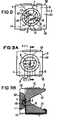
- FIG. 1 ais a diagrammatic, top plan view of a first embodiment of a structural element with a single optoelectronic chip according to the invention
- FIG. 1 bis a schematic representation of a section through the structural element of FIG. 1 taken along the line I—I;
- FIG. 2is a top plan view of a second embodiment of the structural element having at least two optoelectronic chips
- FIG. 3 ais a side-elevational view of a third embodiment of the structural element with emission to a side;
- FIG. 3 bis a section view through the structural element of FIG. 3 a taken along the line III—III shown in FIG. 3 .
- FIG. 1 athere is shown a structural element, more specifically, a light diode structural element.
- the structural elementhas a light-emitting semiconductor chip 1 (LED chip) attached to a chip carrier part 2 of a lead frame 7 by a good heat-conducting material, for example by metal soldering.
- LED chiplight-emitting semiconductor chip
- Three separate external connections 4 , 5 , 6extend outwards in three different directions, starting from the chip carrier part 2 .
- a connection part a with an external connection 9is disposed, which is connected with an electrical contact of the LED chip 1 , e.g., with anode contacting, by use of a bond wire 16 .
- a second contact metallizing (cathode is contacting) of the LED chip 1is located, for example, at its lower side turned to the chip carrier part 2 and is electrically conductively connected with the chip carrier part 2 by an electrically conducting material. Consequently, the chip carrier part 2 with the external connections 4 , 5 , 6 serves in this case as both a cathode connection and as a thermal connection for heat conduction away from the LED chip 1 .
- the cathode contactis not disposed on a lower side of the chip 1 , as in the above mentioned case, but instead on its upper side, for example, it can be connected electrically conductively with the chip carrier part 2 by a bond wire.
- the chip carrier part 2 , the connection part 8 , and partial areas of the external connections 4 , 5 , 6 , 9are encased by an essentially square foundation 10 of a casing 3 , which has a recess 11 ( FIG. 1 b ).
- the recess 11essentially has the form of a truncated cone and extends from a main surface 17 of the foundation 10 running parallel to the lead frame 7 and up to the lead frame 7 . A cross-section of the recess 11 increases from the lead frame 7 to the main surface 17 of the foundation 10 .
- the LED chip 1is located in the recess 11 , which is provided with a radiation-permeable window part 22 , preferably with a transparent plastic sealing. Together with the foundation 10 , the window part 22 forms the casing 3 of the structural element.
- the external connections 4 , 5 , 6 , 9project from the latter on opposite side surfaces 18 , 19 of the foundation 10 .
- the external connections 4 , 5 , 6run apart within the foundation 10 first in a stellate form and then break in their further course, so that they penetrate the side surfaces 18 , 19 perpendicularly.
- the chip carrier part 2preferably lies completely within a floor surface of the recess 11 .
- the external connections 4 , 5 , 6have longitudinal center axes 23 , 24 , 25 in an area in which they run outwards in the stellate form, two adjacent units of which always form an angle of about 90°.
- the external connections 4 , 5 , 6 , 9are bent outside of the foundation 10 first to a second main surface 20 of the foundation 10 opposite the first main surface 17 and in their further course below the foundation 10 to its center. However, as is indicated by the dotted line in FIG. 1 b, they can also be bent to form rocker-shaped connection stumps. This also represents a form of external electrical connection usual in surface assembly technology. These kinds of external connections for surface-mountable structural elements (SMD) are known and therefore will not be illustrated further.
- SMDsurface-mountable structural elements
- the external connections 4 , 5 , 6 , 9are consequently formed so that they all lie simultaneously on the connection or lead plate in the assembled state of the structural element in the lead plate provided for assembling the structural element.
- Inner surfaces of the recess 11form a reflector for the emission radiated by the LED chip 1 in the operation of the structural element. They are optionally coated with a reflection-enhancing material.
- the foundation 10can alternatively consist of a reflection-enhancing material.
- two differently colored lighting LED chips 1 , 13are attached to the chip carrier part 2 of the lead frame 7 by a thermally and electrically conducting material.
- the first 8 and a second connection part 12are disposed on opposite sides of the chip carrier part 2 at a distance from it, each having an external connection 9 , 14 .
- the external connections 9 , 14run displaced parallel to each other; as seen from the chip carrier part 2 , they extend in opposite directions to each other and extend out from the opposite side surfaces 18 , 19 of the foundation 10 . They are electrically conductively connected with the anode contacts of the LED chips 1 , 13 by the bond wires 16 .
- the chip carrier part 2exhibits the two external connections 4 , 5 which, starting from the chip carrier part 2 , likewise extend displaced parallel to each other in opposite directions parallel to the external connections 9 , 14 of the connection parts 8 , 12 and project out on the opposite side surfaces 18 , 19 of the foundation 10 .
- the emission-impermeable foundation 10has the truncated cone recess 11 , which is provided with the transparent window part 22 .
- the LED chips 1 , 13are located in the recess 11 .
- the external connections 4 , 5 , 9 , 14project out of the foundation 10 on the opposite side surfaces 18 , 19 . They are formed outside the foundation 10 analogously to the first embodiment according to FIGS. 1 a and 1 b.
- the casing 3 and the external connections 4 , 5 , 6 , 9 , 14are configured in all cases so that the emission transmitted from the LED chip 1 or chips 1 , 13 in the operation of the structural element is radiated essentially perpendicularly to the assembly surface of the lead plate provided for the assembly of the structural element.
- FIGS. 3 a and 3 brelate to a so-called sideways emitting LED structural element.
- This type of structural elementhas already been explained in the general part of the specification.
- the casing 3 and the external connections 4 , 5 and 9 of the chip carrier part 2 or the connection part 8are configured in this structural element so that it can be attached to the side surface 20 of the foundation 10 to the assembly surface of the lead plate.
- the lead frame 7has the chip carrier part 2 , which has at least two of the external connections 4 , 5 .
- the external connections 4 , 5extend in essentially opposite directions to the outside. In their further course, they break in the same direction, so that they then run parallel to each other in the same direction.
- the connection part 8 with the external connection 9which runs parallel to the two external connections 4 , 5 of the chip carrier part 2 in the same direction that they run, is disposed between the two external connections 4 , 5 of the chip carrier part 2 .
- the chip carrier part 2whose external connections 4 , 5 , and the connection part 8 with the external connection 9 are enclosed by the radiation-impermeable foundation 10 analogously to the first and second embodiments described above, which has the truncated cone recess 11 , is disposed in the LED chip 1 .
- the recess 11is provided with the emission-permeable window part 22 , which preferably consists of an emission-permeable plastic.
- the external connections 4 , 5 , 9which project from it on one and the same side surface 18 of the foundation 10 , are bent downward outside the foundation 10 in the direction of the back side of the foundation 10 and are bent in their further course along a back side 21 of the foundation 10 to its center.
- the outer surfaces of the external connections 4 , 5 , 9 turned away from the side surface 18 of the foundation 10form a support surface of the structural element for its mounting on the lead plate.
- the chip carrier part 2has cooling fin 15 (indicated by dotted line in FIGS. 3 a and 3 b ). It projects out of the side surface 18 , from which the external connections 4 , 5 , 9 project, on the opposite side surface 19 of the foundation 10 and is bent outside the foundation 10 to its back side, so that it lies on the side surface 19 . Further cooling devices can optionally be attached thermally to the cooling fin 15 .
- the external connections of the chip carrier part 2it is preferable for the external connections of the chip carrier part 2 to be wider than the external connections of the connection part or parts 8 , 12 .
- a further improved heat transfer from the LED chip 1can thereby be attained with substantially unchanged housing dimensions.
- the external connections 4 , 5 , 6 , 9 , 14can all have the same width.
- soldering padsare provided on the lead plate provided for the assembly of the structural element in order to attain a further improvement in heat transfer from the LED chip 1 . They are also disposed in the stellate form and can thus distribute the heat conducted from the LED chip 1 over a large surface.
- the lead frames 7 of the structural elements according to the inventionconduct the heat from the LED chip 1 in the stellate form to the outside of the casing 3 . The heat is thereby fed to points in the plate lying far from each other.
- the housing 3 for the LED chips 1 described aboverelates to a housing for optoelectronic structural elements known in semiconductor technology. The separate forms and the materials and manufacturing processes used therefore will not be explained further.
Landscapes
- Led Device Packages (AREA)
- Light Receiving Elements (AREA)
- Packaging Frangible Articles (AREA)
- Cooling Or The Like Of Semiconductors Or Solid State Devices (AREA)
Abstract
Description
Claims (10)
Priority Applications (3)
| Application Number | Priority Date | Filing Date | Title |
|---|---|---|---|
| US10/882,518US7102215B2 (en) | 1997-07-29 | 2004-07-01 | Surface-mountable light-emitting diode structural element |
| US11/397,914US7183632B2 (en) | 1997-07-29 | 2006-04-03 | Surface-mountable light-emitting diode structural element |
| US11/672,092US7508002B2 (en) | 1997-07-29 | 2007-02-07 | Surface-mountable light-emitting diode structural element |
Applications Claiming Priority (8)
| Application Number | Priority Date | Filing Date | Title |
|---|---|---|---|
| DE19732646 | 1997-07-29 | ||
| DE19732646 | 1997-07-29 | ||
| PCT/DE1998/002125WO1999007023A1 (en) | 1997-07-29 | 1998-07-27 | Optoelectronic component |
| US09/494,771US6376902B1 (en) | 1997-07-29 | 2000-01-31 | Optoelectronic structural element |
| US10/072,836US6469321B2 (en) | 1997-07-29 | 2002-02-05 | Surface-mountable light-emitting diode structural element |
| US10/259,556US6573580B2 (en) | 1997-07-29 | 2002-09-27 | Surface-mountable light-emitting diode structural element |
| US10/407,734US6759733B2 (en) | 1997-07-29 | 2003-04-04 | Optoelectric surface-mountable structural element |
| US10/882,518US7102215B2 (en) | 1997-07-29 | 2004-07-01 | Surface-mountable light-emitting diode structural element |
Related Parent Applications (1)
| Application Number | Title | Priority Date | Filing Date |
|---|---|---|---|
| US10/407,734ContinuationUS6759733B2 (en) | 1997-07-29 | 2003-04-04 | Optoelectric surface-mountable structural element |
Related Child Applications (1)
| Application Number | Title | Priority Date | Filing Date |
|---|---|---|---|
| US11/397,914ContinuationUS7183632B2 (en) | 1997-07-29 | 2006-04-03 | Surface-mountable light-emitting diode structural element |
Publications (2)
| Publication Number | Publication Date |
|---|---|
| US20040238930A1 US20040238930A1 (en) | 2004-12-02 |
| US7102215B2true US7102215B2 (en) | 2006-09-05 |
Family
ID=7837261
Family Applications (7)
| Application Number | Title | Priority Date | Filing Date |
|---|---|---|---|
| US09/494,771Expired - LifetimeUS6376902B1 (en) | 1997-07-29 | 2000-01-31 | Optoelectronic structural element |
| US10/072,836Expired - LifetimeUS6469321B2 (en) | 1997-07-29 | 2002-02-05 | Surface-mountable light-emitting diode structural element |
| US10/259,556Expired - LifetimeUS6573580B2 (en) | 1997-07-29 | 2002-09-27 | Surface-mountable light-emitting diode structural element |
| US10/407,734Expired - LifetimeUS6759733B2 (en) | 1997-07-29 | 2003-04-04 | Optoelectric surface-mountable structural element |
| US10/882,518Expired - LifetimeUS7102215B2 (en) | 1997-07-29 | 2004-07-01 | Surface-mountable light-emitting diode structural element |
| US11/397,914Expired - LifetimeUS7183632B2 (en) | 1997-07-29 | 2006-04-03 | Surface-mountable light-emitting diode structural element |
| US11/672,092Expired - Fee RelatedUS7508002B2 (en) | 1997-07-29 | 2007-02-07 | Surface-mountable light-emitting diode structural element |
Family Applications Before (4)
| Application Number | Title | Priority Date | Filing Date |
|---|---|---|---|
| US09/494,771Expired - LifetimeUS6376902B1 (en) | 1997-07-29 | 2000-01-31 | Optoelectronic structural element |
| US10/072,836Expired - LifetimeUS6469321B2 (en) | 1997-07-29 | 2002-02-05 | Surface-mountable light-emitting diode structural element |
| US10/259,556Expired - LifetimeUS6573580B2 (en) | 1997-07-29 | 2002-09-27 | Surface-mountable light-emitting diode structural element |
| US10/407,734Expired - LifetimeUS6759733B2 (en) | 1997-07-29 | 2003-04-04 | Optoelectric surface-mountable structural element |
Family Applications After (2)
| Application Number | Title | Priority Date | Filing Date |
|---|---|---|---|
| US11/397,914Expired - LifetimeUS7183632B2 (en) | 1997-07-29 | 2006-04-03 | Surface-mountable light-emitting diode structural element |
| US11/672,092Expired - Fee RelatedUS7508002B2 (en) | 1997-07-29 | 2007-02-07 | Surface-mountable light-emitting diode structural element |
Country Status (6)
| Country | Link |
|---|---|
| US (7) | US6376902B1 (en) |
| EP (4) | EP1004145B1 (en) |
| JP (5) | JP2001518692A (en) |
| DE (3) | DE29825022U1 (en) |
| TW (1) | TW408460B (en) |
| WO (1) | WO1999007023A1 (en) |
Cited By (15)
| Publication number | Priority date | Publication date | Assignee | Title |
|---|---|---|---|---|
| US20070126098A1 (en)* | 1997-07-29 | 2007-06-07 | Karlheinz Arndt | Surface-mountable light-emitting diode structural element |
| US20070235845A1 (en)* | 2006-03-28 | 2007-10-11 | Cotco Holdings Limited, A Hong Kong Corporation | Apparatus, system and method for use in mounting electronic elements |
| US20100155748A1 (en)* | 2009-01-14 | 2010-06-24 | Cree Hong Kong Limited | Aligned multiple emitter package |
| US8564004B2 (en) | 2011-11-29 | 2013-10-22 | Cree, Inc. | Complex primary optics with intermediate elements |
| USD711840S1 (en) | 2012-06-11 | 2014-08-26 | Cree, Inc. | LED package |
| USD718258S1 (en) | 2012-09-02 | 2014-11-25 | Cree, Inc. | LED package |
| USD718725S1 (en) | 2013-08-01 | 2014-12-02 | Cree, Inc. | LED package with encapsulant |
| USD725613S1 (en) | 2012-06-15 | 2015-03-31 | Cree, Inc. | LED package |
| USD735683S1 (en) | 2013-05-03 | 2015-08-04 | Cree, Inc. | LED package |
| USD758976S1 (en) | 2013-08-08 | 2016-06-14 | Cree, Inc. | LED package |
| US9461024B2 (en) | 2013-08-01 | 2016-10-04 | Cree, Inc. | Light emitter devices and methods for light emitting diode (LED) chips |
| USD777122S1 (en) | 2015-02-27 | 2017-01-24 | Cree, Inc. | LED package |
| USD783547S1 (en) | 2015-06-04 | 2017-04-11 | Cree, Inc. | LED package |
| USD790486S1 (en) | 2014-09-30 | 2017-06-27 | Cree, Inc. | LED package with truncated encapsulant |
| US10256385B2 (en) | 2007-10-31 | 2019-04-09 | Cree, Inc. | Light emitting die (LED) packages and related methods |
Families Citing this family (157)
| Publication number | Priority date | Publication date | Assignee | Title |
|---|---|---|---|---|
| DE19928576C2 (en)* | 1999-06-22 | 2003-05-22 | Osram Opto Semiconductors Gmbh | Surface mountable LED device with improved heat dissipation |
| DE19931689A1 (en) | 1999-07-08 | 2001-01-11 | Patent Treuhand Ges Fuer Elektrische Gluehlampen Mbh | Planar LED assembly on thermally-conductive board, increases cooling, component packing density and life, whilst permitting active device integration to form display- or illumination panel in or on e.g. vehicle |
| DE10002521A1 (en)* | 2000-01-21 | 2001-08-09 | Infineon Technologies Ag | Electro-optical data transmission module |
| ATE324671T1 (en)* | 2000-12-04 | 2006-05-15 | Mu-Chin Yu | LIGHT-EMITTING DIODE WITH IMPROVED HEAT DISSIPATION |
| US6940704B2 (en)* | 2001-01-24 | 2005-09-06 | Gelcore, Llc | Semiconductor light emitting device |
| US20020121683A1 (en)* | 2001-02-27 | 2002-09-05 | Kelly Stephen G. | Encapsulated die package with improved parasitic and thermal performance |
| JP3659635B2 (en)* | 2001-04-10 | 2005-06-15 | 株式会社東芝 | Optical semiconductor device |
| DE10117889A1 (en)* | 2001-04-10 | 2002-10-24 | Osram Opto Semiconductors Gmbh | Leadframe used for a light emitting diode component comprises a chip assembly region, a wire connecting region, external electrical connecting strips, and a support part coupled with a thermal connecting part |
| US20020163001A1 (en)* | 2001-05-04 | 2002-11-07 | Shaddock David Mulford | Surface mount light emitting device package and fabrication method |
| DE10131698A1 (en)* | 2001-06-29 | 2003-01-30 | Osram Opto Semiconductors Gmbh | Surface-mountable radiation-emitting component and method for its production |
| US6843421B2 (en)* | 2001-08-13 | 2005-01-18 | Matrix Semiconductor, Inc. | Molded memory module and method of making the module absent a substrate support |
| US6576983B1 (en)* | 2001-11-13 | 2003-06-10 | Skyworks Solutions, Inc. | Controlled impedance leads in a leadframe for high frequency applications |
| EP1453107A4 (en)* | 2001-11-16 | 2008-12-03 | Toyoda Gosei Kk | LIGHT EMITTING DIODE, DIODE LIGHTING AND LIGHTING DEVICE |
| DE10241989A1 (en)* | 2001-11-30 | 2003-06-18 | Osram Opto Semiconductors Gmbh | Optoelectronic component |
| JP4009097B2 (en)* | 2001-12-07 | 2007-11-14 | 日立電線株式会社 | LIGHT EMITTING DEVICE, ITS MANUFACTURING METHOD, AND LEAD FRAME USED FOR MANUFACTURING LIGHT EMITTING DEVICE |
| USD488137S1 (en) | 2002-01-30 | 2004-04-06 | Nichia Corporation | Light emitting diode |
| JP3875126B2 (en)* | 2002-03-22 | 2007-01-31 | シャープ株式会社 | Semiconductor device and manufacturing method thereof |
| DE10229067B4 (en)* | 2002-06-28 | 2007-08-16 | Osram Opto Semiconductors Gmbh | Optoelectronic component and method for its production |
| JP2004047748A (en)* | 2002-07-12 | 2004-02-12 | Stanley Electric Co Ltd | Light emitting diode |
| TWI292961B (en)* | 2002-09-05 | 2008-01-21 | Nichia Corp | Semiconductor device and an optical device using the semiconductor device |
| US6686609B1 (en)* | 2002-10-01 | 2004-02-03 | Ultrastar Limited | Package structure of surface mounting led and method of manufacturing the same |
| DE10255932A1 (en) | 2002-11-29 | 2004-06-17 | Osram Opto Semiconductors Gmbh | Optoelectronic component |
| US7692206B2 (en)* | 2002-12-06 | 2010-04-06 | Cree, Inc. | Composite leadframe LED package and method of making the same |
| BE1015302A3 (en)* | 2003-01-10 | 2005-01-11 | Glaverbel | Glass with electronic components. |
| WO2004081972A2 (en)* | 2003-03-10 | 2004-09-23 | Osram Opto Semiconductors Gmbh | Housing body, optoelectronic component with a housing body of this type, and plastic housing material |
| DE10323857A1 (en) | 2003-05-26 | 2005-01-27 | Osram Opto Semiconductors Gmbh | Housing for a laser diode device, laser diode device and method of manufacturing a laser diode device |
| JP2008300884A (en)* | 2003-10-30 | 2008-12-11 | Furukawa Electric Co Ltd:The | LED, LED and flat cable connection structure, and LED connection circuit structure |
| KR100999794B1 (en) | 2003-11-03 | 2010-12-08 | 엘지이노텍 주식회사 | Light emitting diode package and manufacturing method thereof |
| KR101311635B1 (en)* | 2003-12-09 | 2013-09-26 | 젤코어 엘엘씨 | Surface mount light emitting chip package |
| JP2005183531A (en)* | 2003-12-17 | 2005-07-07 | Sharp Corp | Semiconductor light emitting device |
| JP4258367B2 (en)* | 2003-12-18 | 2009-04-30 | 株式会社日立製作所 | Optical component mounting package and manufacturing method thereof |
| TWI275189B (en) | 2003-12-30 | 2007-03-01 | Osram Opto Semiconductors Gmbh | Radiation-emitting and/or radiation-receiving semiconductor component and method for producing such component |
| JP2005197329A (en)* | 2004-01-05 | 2005-07-21 | Stanley Electric Co Ltd | Surface mount semiconductor device and lead frame structure thereof |
| US7009285B2 (en)* | 2004-03-19 | 2006-03-07 | Lite-On Technology Corporation | Optoelectronic semiconductor component |
| US20050253159A1 (en)* | 2004-04-28 | 2005-11-17 | Creswick Steven B | Semiconductor (LED) chip attachment |
| US7064424B2 (en)* | 2004-05-06 | 2006-06-20 | Wilson Robert E | Optical surface mount technology package |
| CN100373641C (en)* | 2004-06-15 | 2008-03-05 | 亿光电子工业股份有限公司 | Packaging structure of light emitting diode |
| JP4571139B2 (en)* | 2004-08-10 | 2010-10-27 | ルネサスエレクトロニクス株式会社 | Light emitting device and method for manufacturing light emitting device |
| US20060086945A1 (en)* | 2004-10-27 | 2006-04-27 | Harvatek Corporation | Package structure for optical-electrical semiconductor |
| GB2420221B (en)* | 2004-11-12 | 2009-09-09 | Unity Opto Technology Co Ltd | Solid-state semiconductor light emitting device |
| US9793247B2 (en)* | 2005-01-10 | 2017-10-17 | Cree, Inc. | Solid state lighting component |
| US7821023B2 (en)* | 2005-01-10 | 2010-10-26 | Cree, Inc. | Solid state lighting component |
| US9070850B2 (en) | 2007-10-31 | 2015-06-30 | Cree, Inc. | Light emitting diode package and method for fabricating same |
| US8669572B2 (en) | 2005-06-10 | 2014-03-11 | Cree, Inc. | Power lamp package |
| US7339196B2 (en)* | 2005-06-25 | 2008-03-04 | Industrial Technology Research Institute | Packaging of SMD light emitting diodes |
| KR101187943B1 (en) | 2005-09-20 | 2012-10-05 | 르네사스 일렉트로닉스 가부시키가이샤 | Led light source and method of manufacturing the same |
| JP2007096240A (en)* | 2005-09-30 | 2007-04-12 | Toyoda Gosei Co Ltd | Led lighting device |
| US20070096133A1 (en)* | 2005-11-02 | 2007-05-03 | Lee Kian S | System and method for LED manufacturing |
| JP2007142044A (en)* | 2005-11-16 | 2007-06-07 | Stanley Electric Co Ltd | Semiconductor light emitting device and surface light source using the same |
| USD573113S1 (en) | 2005-12-09 | 2008-07-15 | Nichia Corporation | Light emitting diode |
| KR100719282B1 (en)* | 2005-12-20 | 2007-05-17 | 서울반도체 주식회사 | Top and Side View Common Light Emitting Diodes |
| US7772604B2 (en) | 2006-01-05 | 2010-08-10 | Illumitex | Separate optical device for directing light from an LED |
| US8044412B2 (en) | 2006-01-20 | 2011-10-25 | Taiwan Semiconductor Manufacturing Company, Ltd | Package for a light emitting element |
| US7385285B2 (en)* | 2006-03-29 | 2008-06-10 | Compal Communications, Inc. | Light assembly |
| US20070252161A1 (en)* | 2006-03-31 | 2007-11-01 | 3M Innovative Properties Company | Led mounting structures |
| US8748915B2 (en) | 2006-04-24 | 2014-06-10 | Cree Hong Kong Limited | Emitter package with angled or vertical LED |
| US11210971B2 (en)* | 2009-07-06 | 2021-12-28 | Cree Huizhou Solid State Lighting Company Limited | Light emitting diode display with tilted peak emission pattern |
| US7635915B2 (en)* | 2006-04-26 | 2009-12-22 | Cree Hong Kong Limited | Apparatus and method for use in mounting electronic elements |
| US7655957B2 (en)* | 2006-04-27 | 2010-02-02 | Cree, Inc. | Submounts for semiconductor light emitting device packages and semiconductor light emitting device packages including the same |
| US8044418B2 (en)* | 2006-07-13 | 2011-10-25 | Cree, Inc. | Leadframe-based packages for solid state light emitting devices |
| US7960819B2 (en)* | 2006-07-13 | 2011-06-14 | Cree, Inc. | Leadframe-based packages for solid state emitting devices |
| US8735920B2 (en) | 2006-07-31 | 2014-05-27 | Cree, Inc. | Light emitting diode package with optical element |
| US8367945B2 (en) | 2006-08-16 | 2013-02-05 | Cree Huizhou Opto Limited | Apparatus, system and method for use in mounting electronic elements |
| DE102006046678A1 (en)* | 2006-09-29 | 2008-04-03 | Osram Opto Semiconductors Gmbh | Housing for use with semiconductor body of e.g. LED unit, has plastic-base body with plastic components, where one plastic component is made of material differing from that of other component in optical characteristic |
| WO2008042351A2 (en)* | 2006-10-02 | 2008-04-10 | Illumitex, Inc. | Led system and method |
| TWI311824B (en) | 2006-10-02 | 2009-07-01 | Ind Tech Res Inst | Light emitting diode package structure |
| US20090275266A1 (en)* | 2006-10-02 | 2009-11-05 | Illumitex, Inc. | Optical device polishing |
| JP5303834B2 (en)* | 2006-12-19 | 2013-10-02 | 日亜化学工業株式会社 | Light emitting device |
| TWM315886U (en)* | 2006-12-28 | 2007-07-21 | Everlight Electronics Co Ltd | Light emitting diode structure |
| US7800304B2 (en)* | 2007-01-12 | 2010-09-21 | Avago Technologies Ecbu Ip (Singapore) Pte. Ltd. | Multi-chip packaged LED light source |
| US9711703B2 (en) | 2007-02-12 | 2017-07-18 | Cree Huizhou Opto Limited | Apparatus, system and method for use in mounting electronic elements |
| US7993038B2 (en)* | 2007-03-06 | 2011-08-09 | Toyoda Gosei Co., Ltd. | Light-emitting device |
| JP2007184642A (en)* | 2007-03-28 | 2007-07-19 | Toshiba Electronic Engineering Corp | Optical semiconductor package |
| JP2007184643A (en)* | 2007-03-28 | 2007-07-19 | Toshiba Electronic Engineering Corp | Optical semiconductor package |
| US7964888B2 (en) | 2007-04-18 | 2011-06-21 | Cree, Inc. | Semiconductor light emitting device packages and methods |
| JP5026848B2 (en)* | 2007-04-19 | 2012-09-19 | スタンレー電気株式会社 | Optical semiconductor device and manufacturing method thereof |
| KR100801621B1 (en) | 2007-06-05 | 2008-02-11 | 서울반도체 주식회사 | LED Package |
| CN101388161A (en)* | 2007-09-14 | 2009-03-18 | 科锐香港有限公司 | LED surface mounting device and LED display incorporating the same |
| JP5082710B2 (en)* | 2007-09-19 | 2012-11-28 | 日亜化学工業株式会社 | Light emitting device |
| TWM329244U (en)* | 2007-10-01 | 2008-03-21 | Everlight Electronics Co Ltd | Light emitting diode device |
| US8866169B2 (en)* | 2007-10-31 | 2014-10-21 | Cree, Inc. | LED package with increased feature sizes |
| USD615504S1 (en) | 2007-10-31 | 2010-05-11 | Cree, Inc. | Emitter package |
| USD633631S1 (en) | 2007-12-14 | 2011-03-01 | Cree Hong Kong Limited | Light source of light emitting diode |
| USD634863S1 (en) | 2008-01-10 | 2011-03-22 | Cree Hong Kong Limited | Light source of light emitting diode |
| KR100981214B1 (en)* | 2008-01-28 | 2010-09-10 | 알티전자 주식회사 | LED Package |
| JP2011512037A (en)* | 2008-02-08 | 2011-04-14 | イルミテックス, インコーポレイテッド | System and method for emitter layer shaping |
| JP2009246343A (en)* | 2008-03-11 | 2009-10-22 | Rohm Co Ltd | Semiconductor light-emitting apparatus and method of manufacturing the same |
| DE102008019667A1 (en)* | 2008-04-18 | 2009-10-22 | Ledon Lighting Jennersdorf Gmbh | LED module with a platform with a central recess |
| US8049230B2 (en)* | 2008-05-16 | 2011-11-01 | Cree Huizhou Opto Limited | Apparatus and system for miniature surface mount devices |
| US20100176751A1 (en)* | 2008-05-20 | 2010-07-15 | Panasonic Corporation | Semiconductor light-emitting device as well as light source device and lighting system including the same |
| TW201000806A (en)* | 2008-06-19 | 2010-01-01 | Lighthouse Technology Co Ltd | Light-emitting component and its forming mold |
| JP5464825B2 (en)* | 2008-07-23 | 2014-04-09 | ローム株式会社 | LED module |
| DE102008045925A1 (en)* | 2008-09-04 | 2010-03-11 | Osram Opto Semiconductors Gmbh | Optoelectronic component and method for producing an optoelectronic component |
| DE102008048259B4 (en)* | 2008-09-22 | 2024-10-02 | OSRAM Opto Semiconductors Gesellschaft mit beschränkter Haftung | Housing for an optoelectronic component, side-emitting component with a housing and method for producing a housing |
| KR100982994B1 (en) | 2008-10-15 | 2010-09-17 | 삼성엘이디 주식회사 | LED Package Module |
| US9425172B2 (en)* | 2008-10-24 | 2016-08-23 | Cree, Inc. | Light emitter array |
| US8791471B2 (en) | 2008-11-07 | 2014-07-29 | Cree Hong Kong Limited | Multi-chip light emitting diode modules |
| TW201034256A (en)* | 2008-12-11 | 2010-09-16 | Illumitex Inc | Systems and methods for packaging light-emitting diode devices |
| US20110037083A1 (en)* | 2009-01-14 | 2011-02-17 | Alex Chi Keung Chan | Led package with contrasting face |
| JP5340763B2 (en)* | 2009-02-25 | 2013-11-13 | ローム株式会社 | LED lamp |
| JP2010212322A (en)* | 2009-03-09 | 2010-09-24 | Yazaki Corp | LED unit |
| US8610156B2 (en)* | 2009-03-10 | 2013-12-17 | Lg Innotek Co., Ltd. | Light emitting device package |
| US8089075B2 (en)* | 2009-04-17 | 2012-01-03 | Avago Technologies Ecbu Ip (Singapore) Pte. Ltd. | LFCC package with a reflector cup surrounded by a single encapsulant |
| US8101955B2 (en)* | 2009-04-17 | 2012-01-24 | Avago Technologies Ecbu Ip (Singapore) Pte. Ltd. | PLCC package with a reflector cup surrounded by an encapsulant |
| US8415692B2 (en)* | 2009-07-06 | 2013-04-09 | Cree, Inc. | LED packages with scattering particle regions |
| US8598809B2 (en)* | 2009-08-19 | 2013-12-03 | Cree, Inc. | White light color changing solid state lighting and methods |
| US8585253B2 (en) | 2009-08-20 | 2013-11-19 | Illumitex, Inc. | System and method for color mixing lens array |
| US8449128B2 (en)* | 2009-08-20 | 2013-05-28 | Illumitex, Inc. | System and method for a lens and phosphor layer |
| JP2011071265A (en)* | 2009-09-25 | 2011-04-07 | Toshiba Corp | Light-emitting apparatus |
| US8101962B2 (en)* | 2009-10-06 | 2012-01-24 | Kuang Hong Precision Co., Ltd. | Carrying structure of semiconductor |
| USD622232S1 (en)* | 2009-10-26 | 2010-08-24 | Foxsemicon Integrated Technology, Inc. | Light emitting diode |
| USD624884S1 (en)* | 2009-10-26 | 2010-10-05 | Foxsemicon Integrated Technology, Inc. | Light emitting diode |
| TW201128812A (en) | 2009-12-01 | 2011-08-16 | Lg Innotek Co Ltd | Light emitting device |
| DE102010000942B4 (en)* | 2010-01-15 | 2022-08-25 | Infineon Technologies Ag | Process for manufacturing a power semiconductor module |
| KR101028195B1 (en)* | 2010-01-18 | 2011-04-11 | 엘지이노텍 주식회사 | Light emitting device package and light unit having same |
| US8350370B2 (en)* | 2010-01-29 | 2013-01-08 | Cree Huizhou Opto Limited | Wide angle oval light emitting diode package |
| USD627312S1 (en)* | 2010-02-01 | 2010-11-16 | Foxsemicon Integrated Technology, Inc. | Light-emitting diode |
| USD627311S1 (en)* | 2010-02-01 | 2010-11-16 | Foxsemicon Integrated Technology, Inc. | Light-emitting diode |
| USD627313S1 (en)* | 2010-02-01 | 2010-11-16 | Foxsemicon Integrated Technology, Inc. | Light-emitting diode |
| USD651183S1 (en)* | 2010-02-01 | 2011-12-27 | Foxsemicon Integrated Technology, Inc. | Light-emitting diode |
| USD627314S1 (en)* | 2010-02-01 | 2010-11-16 | Foxsemicon Integrated Technology, Inc. | Light-emitting diode |
| US9468070B2 (en) | 2010-02-16 | 2016-10-11 | Cree Inc. | Color control of light emitting devices and applications thereof |
| US9012938B2 (en) | 2010-04-09 | 2015-04-21 | Cree, Inc. | High reflective substrate of light emitting devices with improved light output |
| KR101705700B1 (en)* | 2010-07-01 | 2017-02-10 | 엘지이노텍 주식회사 | Light Emitting Diode |
| CN101916810B (en)* | 2010-08-06 | 2013-07-03 | 湖北匡通电子股份有限公司 | SMD type LED encapsulation method |
| US20120056218A1 (en)* | 2010-09-08 | 2012-03-08 | Norfidathul Aizar Abdul Karim | Lead frame package with multiple bends |
| JP5667820B2 (en)* | 2010-09-14 | 2015-02-12 | 東芝電子エンジニアリング株式会社 | Optical semiconductor device |
| DE102010045596A1 (en)* | 2010-09-16 | 2012-03-22 | Osram Opto Semiconductors Gmbh | Surface-mountable optoelectronic semiconductor component and lead frame composite |
| CN103155189B (en) | 2010-10-12 | 2017-02-22 | 皇家飞利浦电子股份有限公司 | Highly reflective coating on LED submount |
| US8455882B2 (en) | 2010-10-15 | 2013-06-04 | Cree, Inc. | High efficiency LEDs |
| KR101872521B1 (en)* | 2011-08-25 | 2018-06-28 | 엘지이노텍 주식회사 | Light emitting device package and lighting system having the same |
| JP5850523B2 (en)* | 2011-09-22 | 2016-02-03 | シチズン電子株式会社 | LED chip |
| CN102306697A (en)* | 2011-09-29 | 2012-01-04 | 昆山市华英精密模具工业有限公司 | Ultra-thin-type LED (light emitting diode) support with heat-radiation bottom |
| US8823041B2 (en) | 2011-10-27 | 2014-09-02 | Seoul Semiconductor Co., Ltd. | Light emitting diode package and light emitting module comprising the same |
| US8692282B2 (en) | 2011-10-27 | 2014-04-08 | Seoul Semiconductor Co., Ltd. | Light emitting diode package and light emitting module comprising the same |
| JP5254422B2 (en)* | 2011-10-31 | 2013-08-07 | ルネサスエレクトロニクス株式会社 | LED light source |
| US8858025B2 (en)* | 2012-03-07 | 2014-10-14 | Lg Innotek Co., Ltd. | Lighting device |
| KR101944409B1 (en) | 2012-06-08 | 2019-04-17 | 엘지이노텍 주식회사 | A light emitting device package |
| JP6192987B2 (en)* | 2012-06-12 | 2017-09-06 | エルジー イノテック カンパニー リミテッド | Lighting device |
| JP6275399B2 (en) | 2012-06-18 | 2018-02-07 | エルジー イノテック カンパニー リミテッド | Lighting device |
| US9627595B2 (en)* | 2012-06-27 | 2017-04-18 | Lg Innotek Co., Ltd. | Lighting device |
| JP6282419B2 (en)* | 2012-07-27 | 2018-02-21 | エルジー イノテック カンパニー リミテッド | Lighting device |
| DE202012009560U1 (en)* | 2012-10-08 | 2014-01-09 | Oechsler Aktiengesellschaft | Event detector and medication donor with such event detector |
| CN103594605A (en)* | 2013-11-05 | 2014-02-19 | 广东长盈精密技术有限公司 | LED photoelectric component |
| JP5740458B2 (en)* | 2013-12-02 | 2015-06-24 | 東芝電子エンジニアリング株式会社 | Optical semiconductor package |
| CN103779485B (en)* | 2014-01-28 | 2017-01-18 | 深圳市蓝科电子有限公司 | Outdoor SMD full-color LED lamp bead and manufacturing method thereof |
| US9601670B2 (en) | 2014-07-11 | 2017-03-21 | Cree, Inc. | Method to form primary optic with variable shapes and/or geometries without a substrate |
| JP2016039213A (en)* | 2014-08-06 | 2016-03-22 | ローム株式会社 | Substrate built-in package, semiconductor device, and module |
| US10622522B2 (en) | 2014-09-05 | 2020-04-14 | Theodore Lowes | LED packages with chips having insulated surfaces |
| DE102015105692A1 (en)* | 2015-04-14 | 2016-10-20 | Osram Opto Semiconductors Gmbh | Semiconductor device and method for producing a plurality of semiconductor devices |
| CN106571383B (en) | 2015-10-08 | 2020-04-28 | 联华电子股份有限公司 | Semiconductor element and manufacturing method thereof |
| DE102016106570A1 (en)* | 2016-04-11 | 2017-10-12 | Osram Opto Semiconductors Gmbh | A light-emitting semiconductor chip, light-emitting component and method for producing a light-emitting component |
| JP2018142436A (en)* | 2017-02-27 | 2018-09-13 | パナソニックIpマネジメント株式会社 | Light source module, lighting device, and moving body |
| JP6680274B2 (en)* | 2017-06-27 | 2020-04-15 | 日亜化学工業株式会社 | Light emitting device and lead frame with resin |
| TWI713237B (en)* | 2018-08-01 | 2020-12-11 | 大陸商光寶光電(常州)有限公司 | Led package structure |
| CN110828438B (en)* | 2018-08-13 | 2025-08-08 | 光宝光电(常州)有限公司 | Light-emitting diode packaging structure |
| US11227985B2 (en)* | 2019-03-28 | 2022-01-18 | Nichia Corporation | Light-emitting device |
Citations (69)
| Publication number | Priority date | Publication date | Assignee | Title |
|---|---|---|---|---|
| DE1915290A1 (en) | 1968-03-28 | 1969-10-02 | Gen Electric | Light emitting device |
| US3573568A (en) | 1969-06-18 | 1971-04-06 | Gen Electric | Light emitting semiconductor chips mounted in a slotted substrate forming a display apparatus |
| DE7128442U (en) | 1971-07-23 | 1971-12-30 | Siemens Ag | HERMETICALLY LOCKED HOUSING FOR SEMICONDUCTOR ELEMENTS |
| US3742833A (en) | 1971-06-14 | 1973-07-03 | J Sewell | System for optically encoding an item and verifying same |
| US3774086A (en) | 1972-09-25 | 1973-11-20 | Gen Electric | Solid state lamp having visible-emitting phosphor at edge of infrated-emitting element |
| US3976877A (en) | 1974-02-22 | 1976-08-24 | U.S. Philips Corporation | Opto-electronic photocoupling device and method of manufacturing same |
| JPS51145288A (en) | 1975-06-09 | 1976-12-14 | Seiko Epson Corp | Solar cell |
| JPS5368992A (en) | 1976-12-02 | 1978-06-19 | Mitsubishi Electric Corp | Semiconductor device and its production |
| DE2829260A1 (en) | 1978-07-04 | 1980-01-24 | Licentia Gmbh | Photodiode with substrate embedded in transparent housing - has parallel conductors in infrared filter housing with plastics cap |
| US4203792A (en) | 1977-11-17 | 1980-05-20 | Bell Telephone Laboratories, Incorporated | Method for the fabrication of devices including polymeric materials |
| US4307297A (en) | 1978-09-12 | 1981-12-22 | U.S. Philips Corporation | Opto-electronic device |
| JPS58194382A (en) | 1982-05-08 | 1983-11-12 | Matsushita Electric Ind Co Ltd | Electrode structure for semiconductor device |
| DE3227645A1 (en) | 1982-07-23 | 1984-01-26 | Siemens AG, 1000 Berlin und 8000 München | Electronic component and a method for its production |
| JPS6090680A (en) | 1983-10-21 | 1985-05-21 | 東京システムクリエート株式会社 | Electric stapler |
| JPS61248839A (en) | 1985-04-26 | 1986-11-06 | Nippon Kogaku Kk <Nikon> | Takeout device for housed wafer |
| JPS62263663A (en) | 1986-05-12 | 1987-11-16 | Hitachi Tobu Semiconductor Ltd | Electronic device |
| JPS62263667A (en) | 1986-05-12 | 1987-11-16 | Hitachi Tobu Semiconductor Ltd | electronic equipment |
| US4727457A (en) | 1986-01-24 | 1988-02-23 | U.S. Philips Corporation | Surface-mounted optoelectronic device |
| JPS6352455A (en) | 1986-08-22 | 1988-03-05 | Hitachi Ltd | Lead frame for sealed semiconductor device |
| US4780795A (en) | 1986-04-28 | 1988-10-25 | Burr-Brown Corporation | Packages for hybrid integrated circuit high voltage isolation amplifiers and method of manufacture |
| JPH01117227A (en) | 1988-09-27 | 1989-05-10 | Matsushita Electric Works Ltd | High-frequency current switching relay |
| US4843280A (en) | 1988-01-15 | 1989-06-27 | Siemens Corporate Research & Support, Inc. | A modular surface mount component for an electrical device or led's |
| US4851695A (en) | 1986-09-30 | 1989-07-25 | Siemens Aktiengesellschaft | Optoelectronic coupling element with transparent spacer elements |
| US4875750A (en) | 1987-02-25 | 1989-10-24 | Siemens Aktiengesellschaft | Optoelectronic coupling element and method for its manufacture |
| EP0373003A2 (en) | 1988-12-09 | 1990-06-13 | Molex Incorporated | Surface-mounted component's contact having a soldering portion |
| JPH02156558A (en) | 1988-12-08 | 1990-06-15 | Sharp Corp | Lead frame of semiconductor device and manufacture of semiconductor device using same |
| US4935856A (en) | 1989-10-05 | 1990-06-19 | Dialight Corporation | Surface mounted LED package |
| EP0400176A1 (en) | 1989-05-31 | 1990-12-05 | Siemens Aktiengesellschaft | Surface-mountable optical element |
| US5014418A (en) | 1989-07-13 | 1991-05-14 | Gte Products Corporation | Method of forming a two piece chip carrier |
| JPH03171682A (en) | 1989-11-29 | 1991-07-25 | Iwasaki Electric Co Ltd | Light emitting diode |
| US5035483A (en) | 1989-05-31 | 1991-07-30 | Siemens Aktiengesellschaft | Surface-mountable opto-component |
| JPH03250657A (en) | 1990-02-28 | 1991-11-08 | Hitachi Ltd | Resin-sealed semiconductor device with both surfaces packaged |
| JPH03287690A (en) | 1990-04-04 | 1991-12-18 | Kasei Optonix Co Ltd | Phosphor manufacturing method and fluorescent lamp using the same |
| JPH0462942A (en) | 1990-06-30 | 1992-02-27 | Nec Corp | Semiconductor device |
| JPH0467462A (en) | 1990-07-06 | 1992-03-03 | Nippon Chemicon Corp | Disk drive device |
| US5093713A (en) | 1989-01-30 | 1992-03-03 | Kabushiki Kaisha Toshiba | Semiconductor device package |
| JPH04128811A (en) | 1990-09-20 | 1992-04-30 | Nec Corp | Photoelectric conversion device |
| JPH04139732A (en) | 1990-09-29 | 1992-05-13 | Nec Corp | Manufacture of semiconductor device |
| US5146310A (en) | 1989-10-16 | 1992-09-08 | National Semiconductor Corp. | Thermally enhanced leadframe |
| EP0532974A2 (en) | 1991-09-17 | 1993-03-24 | Hosiden Corporation | Electrical parts for surface mounting |
| USRE34254E (en) | 1989-10-05 | 1993-05-18 | Dialight Corporation | Surface mounted LED package |
| JPH05315653A (en) | 1992-05-08 | 1993-11-26 | Denki Kagaku Kogyo Kk | Matrix display board |
| JPH05315652A (en) | 1992-04-02 | 1993-11-26 | Nec Corp | Optical semiconductor device |
| US5289344A (en) | 1992-10-08 | 1994-02-22 | Allegro Microsystems Inc. | Integrated-circuit lead-frame package with failure-resistant ground-lead and heat-sink means |
| JPH0653554A (en) | 1992-07-28 | 1994-02-25 | Rohm Co Ltd | Optical semiconductor device |
| US5294897A (en) | 1992-07-20 | 1994-03-15 | Mitsubishi Denki Kabushiki Kaisha | Microwave IC package |
| JPH06163083A (en) | 1992-11-17 | 1994-06-10 | Sharp Corp | Secondary battery charged state monitoring system in electronic apparatus |
| JPH06204570A (en) | 1993-09-29 | 1994-07-22 | Rohm Co Ltd | Manufacture of luminous display |
| JPH06204604A (en) | 1993-01-06 | 1994-07-22 | Sanyo Electric Co Ltd | Semiconductor laser device |
| US5367124A (en) | 1993-06-28 | 1994-11-22 | International Business Machines Corporation | Compliant lead for surface mounting a chip package to a substrate |
| EP0646971A2 (en) | 1993-09-30 | 1995-04-05 | Siemens Aktiengesellschaft | Two-terminal SMT-miniature-housing of semiconductor device and process of manufacturing the same |
| JPH07176794A (en) | 1993-12-17 | 1995-07-14 | Nichia Chem Ind Ltd | Surface light source |
| JPH07335980A (en) | 1994-06-07 | 1995-12-22 | Fuji Electric Co Ltd | Semiconductor laser device |
| US5479050A (en) | 1990-10-18 | 1995-12-26 | Texas Instruments Incorporated | Leadframe with pedestal |
| JPH087614A (en) | 1994-06-17 | 1996-01-12 | Nichia Chem Ind Ltd | Surface light source |
| DE4446566A1 (en) | 1994-12-24 | 1996-06-27 | Telefunken Microelectron | Multipole, surface-mountable, electronic component |
| US5543657A (en) | 1994-10-07 | 1996-08-06 | International Business Machines Corporation | Single layer leadframe design with groundplane capability |
| US5608553A (en) | 1995-07-24 | 1997-03-04 | Samsung Display Devices Co., Ltd. | Back light for a liquid crystal display |
| DE19536454A1 (en) | 1995-09-29 | 1997-04-03 | Siemens Ag | Optoelectronic semiconductor component |
| US5659950A (en) | 1995-03-23 | 1997-08-26 | Motorola, Inc. | Method of forming a package assembly |
| US5685071A (en) | 1995-06-05 | 1997-11-11 | Hughes Electronics | Method of constructing a sealed chip-on-board electronic module |
| JPH09303981A (en) | 1996-05-08 | 1997-11-28 | Nec Corp | Heat pipe heat radiating device |
| WO1998020718A1 (en) | 1996-11-06 | 1998-05-14 | Siliconix Incorporated | Heat sink-lead frame structure |
| US5844305A (en) | 1994-01-13 | 1998-12-01 | Samsung Electronics Co., Ltd. | Lead frame for semiconductor devices |
| US5863810A (en) | 1994-05-09 | 1999-01-26 | Euratec B.V. | Method for encapsulating an integrated circuit having a window |
| US5907151A (en) | 1996-05-24 | 1999-05-25 | Siemens Aktiengesellschaft | Surface mountable optoelectronic transducer and method for its production |
| US6066861A (en) | 1996-09-20 | 2000-05-23 | Siemens Aktiengesellschaft | Wavelength-converting casting composition and its use |
| JP3250657B2 (en) | 1997-03-07 | 2002-01-28 | ダイハツ工業株式会社 | Automotive defroster |
| US6376902B1 (en)* | 1997-07-29 | 2002-04-23 | Osram Opto Semiconductors Gmbh & Co. Ohg | Optoelectronic structural element |
Family Cites Families (14)
| Publication number | Priority date | Publication date | Assignee | Title |
|---|---|---|---|---|
| US34254A (en)* | 1862-01-28 | Improvement in metallic roofing | ||
| US4273040A (en) | 1979-09-28 | 1981-06-16 | International Business Machines Corporation | Segmented drum bar helix printer |
| JPS58190051A (en) | 1982-02-16 | 1983-11-05 | フエアチアイルド・カメラ・アンド・インストルメント・コ−ポレ−シヨン | Lead frame for integrated circuit improved for heat sink effect |
| JPS6081877A (en)* | 1983-10-12 | 1985-05-09 | Sharp Corp | Optical coupling semiconductor device |
| JPH01302874A (en) | 1988-05-31 | 1989-12-06 | Matsushita Electron Corp | Optical semiconductor device |
| JP2535651B2 (en)* | 1990-07-24 | 1996-09-18 | 株式会社東芝 | Semiconductor device |
| JPH04163973A (en)* | 1990-10-27 | 1992-06-09 | Toyoda Gosei Co Ltd | variable color light emitting diode |
| GB9304919D0 (en)* | 1993-03-10 | 1993-04-28 | Celltech Ltd | Chemical compounds |
| JP3227295B2 (en)* | 1993-12-28 | 2001-11-12 | 松下電工株式会社 | Light emitting diode manufacturing method |
| JPH07235624A (en) | 1994-02-23 | 1995-09-05 | Toyoda Gosei Co Ltd | Led lamp |
| JPH07281619A (en)* | 1994-04-04 | 1995-10-27 | Rohm Co Ltd | LED lamp and its mounting structure on the board |
| US5519576A (en)* | 1994-07-19 | 1996-05-21 | Analog Devices, Inc. | Thermally enhanced leadframe |
| US5489800A (en) | 1994-08-31 | 1996-02-06 | Motorola, Inc. | Dual channel small outline optocoupler package and method thereof |
| JPH09321341A (en)* | 1996-05-30 | 1997-12-12 | Nichia Chem Ind Ltd | Optical semiconductor device and manufacturing method thereof |
- 1998
- 1998-07-27DEDE29825022Upatent/DE29825022U1/ennot_activeExpired - Lifetime
- 1998-07-27DEDE59812835Tpatent/DE59812835D1/ennot_activeExpired - Lifetime
- 1998-07-27EPEP98947353Apatent/EP1004145B1/ennot_activeExpired - Lifetime
- 1998-07-27DEDE29825062Upatent/DE29825062U1/ennot_activeExpired - Lifetime
- 1998-07-27EPEP05011759.7Apatent/EP1566846B1/ennot_activeExpired - Lifetime
- 1998-07-27EPEP10181078.6Apatent/EP2267798B1/ennot_activeExpired - Lifetime
- 1998-07-27WOPCT/DE1998/002125patent/WO1999007023A1/enactiveIP Right Grant
- 1998-07-27JPJP2000505656Apatent/JP2001518692A/enactivePending
- 1998-07-27EPEP10181067Apatent/EP2267797A1/ennot_activeWithdrawn
- 1998-07-29TWTW087112433Apatent/TW408460B/ennot_activeIP Right Cessation
- 2000
- 2000-01-31USUS09/494,771patent/US6376902B1/ennot_activeExpired - Lifetime
- 2002
- 2002-02-05USUS10/072,836patent/US6469321B2/ennot_activeExpired - Lifetime
- 2002-09-27USUS10/259,556patent/US6573580B2/ennot_activeExpired - Lifetime
- 2003
- 2003-04-04USUS10/407,734patent/US6759733B2/ennot_activeExpired - Lifetime
- 2004
- 2004-07-01USUS10/882,518patent/US7102215B2/ennot_activeExpired - Lifetime
- 2006
- 2006-04-03USUS11/397,914patent/US7183632B2/ennot_activeExpired - Lifetime
- 2006-10-30JPJP2006294396Apatent/JP2007036293A/enactivePending
- 2006-10-30JPJP2006294398Apatent/JP2007036295A/enactivePending
- 2006-10-30JPJP2006294397Apatent/JP2007036294A/enactivePending
- 2007
- 2007-02-07USUS11/672,092patent/US7508002B2/ennot_activeExpired - Fee Related
- 2009
- 2009-04-02JPJP2009089977Apatent/JP2009152639A/enactivePending
Patent Citations (78)
| Publication number | Priority date | Publication date | Assignee | Title |
|---|---|---|---|---|
| DE1915290A1 (en) | 1968-03-28 | 1969-10-02 | Gen Electric | Light emitting device |
| FR2004989A1 (en) | 1968-03-28 | 1969-12-05 | Gen Electric | |
| US3529200A (en) | 1968-03-28 | 1970-09-15 | Gen Electric | Light-emitting phosphor-diode combination |
| US3573568A (en) | 1969-06-18 | 1971-04-06 | Gen Electric | Light emitting semiconductor chips mounted in a slotted substrate forming a display apparatus |
| US3742833A (en) | 1971-06-14 | 1973-07-03 | J Sewell | System for optically encoding an item and verifying same |
| DE7128442U (en) | 1971-07-23 | 1971-12-30 | Siemens Ag | HERMETICALLY LOCKED HOUSING FOR SEMICONDUCTOR ELEMENTS |
| US3774086A (en) | 1972-09-25 | 1973-11-20 | Gen Electric | Solid state lamp having visible-emitting phosphor at edge of infrated-emitting element |
| DE2347289A1 (en) | 1972-09-25 | 1974-04-18 | Gen Electric | SOLID STATE LAMP FOR VISIBLE INFRARED |
| US3976877A (en) | 1974-02-22 | 1976-08-24 | U.S. Philips Corporation | Opto-electronic photocoupling device and method of manufacturing same |
| JPS51145288A (en) | 1975-06-09 | 1976-12-14 | Seiko Epson Corp | Solar cell |
| JPS5368992A (en) | 1976-12-02 | 1978-06-19 | Mitsubishi Electric Corp | Semiconductor device and its production |
| US4203792A (en) | 1977-11-17 | 1980-05-20 | Bell Telephone Laboratories, Incorporated | Method for the fabrication of devices including polymeric materials |
| DE2829260A1 (en) | 1978-07-04 | 1980-01-24 | Licentia Gmbh | Photodiode with substrate embedded in transparent housing - has parallel conductors in infrared filter housing with plastics cap |
| US4307297A (en) | 1978-09-12 | 1981-12-22 | U.S. Philips Corporation | Opto-electronic device |
| JPS58194382A (en) | 1982-05-08 | 1983-11-12 | Matsushita Electric Ind Co Ltd | Electrode structure for semiconductor device |
| DE3227645A1 (en) | 1982-07-23 | 1984-01-26 | Siemens AG, 1000 Berlin und 8000 München | Electronic component and a method for its production |
| JPS6090680A (en) | 1983-10-21 | 1985-05-21 | 東京システムクリエート株式会社 | Electric stapler |
| JPS61248839A (en) | 1985-04-26 | 1986-11-06 | Nippon Kogaku Kk <Nikon> | Takeout device for housed wafer |
| US4727457A (en) | 1986-01-24 | 1988-02-23 | U.S. Philips Corporation | Surface-mounted optoelectronic device |
| US4780795A (en) | 1986-04-28 | 1988-10-25 | Burr-Brown Corporation | Packages for hybrid integrated circuit high voltage isolation amplifiers and method of manufacture |
| JPS62263667A (en) | 1986-05-12 | 1987-11-16 | Hitachi Tobu Semiconductor Ltd | electronic equipment |
| JPS62263663A (en) | 1986-05-12 | 1987-11-16 | Hitachi Tobu Semiconductor Ltd | Electronic device |
| JPS6352455A (en) | 1986-08-22 | 1988-03-05 | Hitachi Ltd | Lead frame for sealed semiconductor device |
| US4851695A (en) | 1986-09-30 | 1989-07-25 | Siemens Aktiengesellschaft | Optoelectronic coupling element with transparent spacer elements |
| US4875750A (en) | 1987-02-25 | 1989-10-24 | Siemens Aktiengesellschaft | Optoelectronic coupling element and method for its manufacture |
| US4843280A (en) | 1988-01-15 | 1989-06-27 | Siemens Corporate Research & Support, Inc. | A modular surface mount component for an electrical device or led's |
| JPH01117227A (en) | 1988-09-27 | 1989-05-10 | Matsushita Electric Works Ltd | High-frequency current switching relay |
| JPH02156558A (en) | 1988-12-08 | 1990-06-15 | Sharp Corp | Lead frame of semiconductor device and manufacture of semiconductor device using same |
| EP0373003A2 (en) | 1988-12-09 | 1990-06-13 | Molex Incorporated | Surface-mounted component's contact having a soldering portion |
| US4955820A (en) | 1988-12-09 | 1990-09-11 | Molex Incorporated | T-leg SMT contact |
| US5093713A (en) | 1989-01-30 | 1992-03-03 | Kabushiki Kaisha Toshiba | Semiconductor device package |
| US5035483A (en) | 1989-05-31 | 1991-07-30 | Siemens Aktiengesellschaft | Surface-mountable opto-component |
| EP0400176A1 (en) | 1989-05-31 | 1990-12-05 | Siemens Aktiengesellschaft | Surface-mountable optical element |
| US5014418A (en) | 1989-07-13 | 1991-05-14 | Gte Products Corporation | Method of forming a two piece chip carrier |
| US4935856A (en) | 1989-10-05 | 1990-06-19 | Dialight Corporation | Surface mounted LED package |
| USRE34254E (en) | 1989-10-05 | 1993-05-18 | Dialight Corporation | Surface mounted LED package |
| US5146310A (en) | 1989-10-16 | 1992-09-08 | National Semiconductor Corp. | Thermally enhanced leadframe |
| JPH03171682A (en) | 1989-11-29 | 1991-07-25 | Iwasaki Electric Co Ltd | Light emitting diode |
| JPH03250657A (en) | 1990-02-28 | 1991-11-08 | Hitachi Ltd | Resin-sealed semiconductor device with both surfaces packaged |
| JPH03287690A (en) | 1990-04-04 | 1991-12-18 | Kasei Optonix Co Ltd | Phosphor manufacturing method and fluorescent lamp using the same |
| JPH0462942A (en) | 1990-06-30 | 1992-02-27 | Nec Corp | Semiconductor device |
| JPH0467462A (en) | 1990-07-06 | 1992-03-03 | Nippon Chemicon Corp | Disk drive device |
| JPH04128811A (en) | 1990-09-20 | 1992-04-30 | Nec Corp | Photoelectric conversion device |
| JPH04139732A (en) | 1990-09-29 | 1992-05-13 | Nec Corp | Manufacture of semiconductor device |
| US5479050A (en) | 1990-10-18 | 1995-12-26 | Texas Instruments Incorporated | Leadframe with pedestal |
| EP0532974A2 (en) | 1991-09-17 | 1993-03-24 | Hosiden Corporation | Electrical parts for surface mounting |
| US5273460A (en) | 1991-09-17 | 1993-12-28 | Hosiden Corporation | Electrical parts for surface mounting |
| JPH05315652A (en) | 1992-04-02 | 1993-11-26 | Nec Corp | Optical semiconductor device |
| JPH05315653A (en) | 1992-05-08 | 1993-11-26 | Denki Kagaku Kogyo Kk | Matrix display board |
| US5294897A (en) | 1992-07-20 | 1994-03-15 | Mitsubishi Denki Kabushiki Kaisha | Microwave IC package |
| JPH0653554A (en) | 1992-07-28 | 1994-02-25 | Rohm Co Ltd | Optical semiconductor device |
| US5289344A (en) | 1992-10-08 | 1994-02-22 | Allegro Microsystems Inc. | Integrated-circuit lead-frame package with failure-resistant ground-lead and heat-sink means |
| JPH06163083A (en) | 1992-11-17 | 1994-06-10 | Sharp Corp | Secondary battery charged state monitoring system in electronic apparatus |
| JPH06204604A (en) | 1993-01-06 | 1994-07-22 | Sanyo Electric Co Ltd | Semiconductor laser device |
| US5367124A (en) | 1993-06-28 | 1994-11-22 | International Business Machines Corporation | Compliant lead for surface mounting a chip package to a substrate |
| JPH06204570A (en) | 1993-09-29 | 1994-07-22 | Rohm Co Ltd | Manufacture of luminous display |
| EP0646971A2 (en) | 1993-09-30 | 1995-04-05 | Siemens Aktiengesellschaft | Two-terminal SMT-miniature-housing of semiconductor device and process of manufacturing the same |
| JPH07176794A (en) | 1993-12-17 | 1995-07-14 | Nichia Chem Ind Ltd | Surface light source |
| US5844305A (en) | 1994-01-13 | 1998-12-01 | Samsung Electronics Co., Ltd. | Lead frame for semiconductor devices |
| US5863810A (en) | 1994-05-09 | 1999-01-26 | Euratec B.V. | Method for encapsulating an integrated circuit having a window |
| JPH07335980A (en) | 1994-06-07 | 1995-12-22 | Fuji Electric Co Ltd | Semiconductor laser device |
| JPH087614A (en) | 1994-06-17 | 1996-01-12 | Nichia Chem Ind Ltd | Surface light source |
| US5543657A (en) | 1994-10-07 | 1996-08-06 | International Business Machines Corporation | Single layer leadframe design with groundplane capability |
| US5706177A (en) | 1994-12-24 | 1998-01-06 | Temic Telefunken Microelectronic Gmbh | Multi-terminal surface-mounted electronic device |
| DE4446566A1 (en) | 1994-12-24 | 1996-06-27 | Telefunken Microelectron | Multipole, surface-mountable, electronic component |
| US5659950A (en) | 1995-03-23 | 1997-08-26 | Motorola, Inc. | Method of forming a package assembly |
| US5685071A (en) | 1995-06-05 | 1997-11-11 | Hughes Electronics | Method of constructing a sealed chip-on-board electronic module |
| US5608553A (en) | 1995-07-24 | 1997-03-04 | Samsung Display Devices Co., Ltd. | Back light for a liquid crystal display |
| DE19536454A1 (en) | 1995-09-29 | 1997-04-03 | Siemens Ag | Optoelectronic semiconductor component |
| JPH09303981A (en) | 1996-05-08 | 1997-11-28 | Nec Corp | Heat pipe heat radiating device |
| US5907151A (en) | 1996-05-24 | 1999-05-25 | Siemens Aktiengesellschaft | Surface mountable optoelectronic transducer and method for its production |
| US6066861A (en) | 1996-09-20 | 2000-05-23 | Siemens Aktiengesellschaft | Wavelength-converting casting composition and its use |
| WO1998020718A1 (en) | 1996-11-06 | 1998-05-14 | Siliconix Incorporated | Heat sink-lead frame structure |
| JP3250657B2 (en) | 1997-03-07 | 2002-01-28 | ダイハツ工業株式会社 | Automotive defroster |
| US6376902B1 (en)* | 1997-07-29 | 2002-04-23 | Osram Opto Semiconductors Gmbh & Co. Ohg | Optoelectronic structural element |
| US6469321B2 (en)* | 1997-07-29 | 2002-10-22 | Osram Opto Semiconductors Gmbh & Co. Ohg | Surface-mountable light-emitting diode structural element |
| US6573580B2 (en)* | 1997-07-29 | 2003-06-03 | Osram Opto Semiconductors Gmbh & Co. Ohg | Surface-mountable light-emitting diode structural element |
| US6759733B2 (en)* | 1997-07-29 | 2004-07-06 | Osram Opto Semiconductors Gmbh | Optoelectric surface-mountable structural element |
Non-Patent Citations (8)
| Title |
|---|
| "LED im Miniatur-Kunststoffgeh�use SOT-23 f�r Oberfl�chenmontage" [LED in miniature plastic housing SOT-23 for surface mounting], Siemens Components 22 (1984), vol. 2, p. 97. |
| "LED im Miniatur-Kunststoffgehäuse SOT-23 für Oberflächenmontage" [LED in miniature plastic housing SOT-23 for surface mounting], Siemens Components 22 (1984), vol. 2, p. 97. |
| In the Matter of Certain Light-Emitting Diodes and Products Containing Same, Investigation No. 337-TA-512, "Commission Opinion," (Public Verison), Dated Aug. 29, 2005. |
| In the Matter of Certain Light-Emitting Diodes and Products Containing Same, Investigation No. 337-TA-512, "Initial Determination on Violation of Section 337 and Recommended Determination on Remedy and Bond," (Public Version), Dated May 10, 2005. |
| In the Matter of Certain Light-Emitting Diodes and Products Containing Same, Investigation No. 337-TA-512, "Notice of Commission Final Determination of No Violation of Section 337 as to One Patent and Determination to Remand the Investigation as Certain Other Patents," Dated Aug. 10, 2005. |
| In the Matter of Certain Light-Emitting Diodes and Products Containing Same, Investigation No. 337-TA-512, "Open Session," pp. 562-575, Dated Dec. 9, 2004. |
| Patent Abstracts of Japan No. 60-081877 (Ikuo), dated May 9, 1985. |
| Patents Abstracts of Japan No. 06-204604 (Taro), dated Jul. 22, 1994. |
Cited By (20)
| Publication number | Priority date | Publication date | Assignee | Title |
|---|---|---|---|---|
| US7508002B2 (en) | 1997-07-29 | 2009-03-24 | Osram Gmbh | Surface-mountable light-emitting diode structural element |
| US20070126098A1 (en)* | 1997-07-29 | 2007-06-07 | Karlheinz Arndt | Surface-mountable light-emitting diode structural element |
| US9035439B2 (en)* | 2006-03-28 | 2015-05-19 | Cree Huizhou Solid State Lighting Company Limited | Apparatus, system and method for use in mounting electronic elements |
| US20070235845A1 (en)* | 2006-03-28 | 2007-10-11 | Cotco Holdings Limited, A Hong Kong Corporation | Apparatus, system and method for use in mounting electronic elements |
| US7675145B2 (en)* | 2006-03-28 | 2010-03-09 | Cree Hong Kong Limited | Apparatus, system and method for use in mounting electronic elements |
| US10256385B2 (en) | 2007-10-31 | 2019-04-09 | Cree, Inc. | Light emitting die (LED) packages and related methods |
| US20100155748A1 (en)* | 2009-01-14 | 2010-06-24 | Cree Hong Kong Limited | Aligned multiple emitter package |
| US8368112B2 (en) | 2009-01-14 | 2013-02-05 | Cree Huizhou Opto Limited | Aligned multiple emitter package |
| US9722158B2 (en) | 2009-01-14 | 2017-08-01 | Cree Huizhou Solid State Lighting Company Limited | Aligned multiple emitter package |
| US8564004B2 (en) | 2011-11-29 | 2013-10-22 | Cree, Inc. | Complex primary optics with intermediate elements |
| USD711840S1 (en) | 2012-06-11 | 2014-08-26 | Cree, Inc. | LED package |
| USD725613S1 (en) | 2012-06-15 | 2015-03-31 | Cree, Inc. | LED package |
| USD718258S1 (en) | 2012-09-02 | 2014-11-25 | Cree, Inc. | LED package |
| USD735683S1 (en) | 2013-05-03 | 2015-08-04 | Cree, Inc. | LED package |
| US9461024B2 (en) | 2013-08-01 | 2016-10-04 | Cree, Inc. | Light emitter devices and methods for light emitting diode (LED) chips |
| USD718725S1 (en) | 2013-08-01 | 2014-12-02 | Cree, Inc. | LED package with encapsulant |
| USD758976S1 (en) | 2013-08-08 | 2016-06-14 | Cree, Inc. | LED package |
| USD790486S1 (en) | 2014-09-30 | 2017-06-27 | Cree, Inc. | LED package with truncated encapsulant |
| USD777122S1 (en) | 2015-02-27 | 2017-01-24 | Cree, Inc. | LED package |
| USD783547S1 (en) | 2015-06-04 | 2017-04-11 | Cree, Inc. | LED package |
Also Published As
| Publication number | Publication date |
|---|---|
| US7508002B2 (en) | 2009-03-24 |
| EP2267798A1 (en) | 2010-12-29 |
| US20030189236A1 (en) | 2003-10-09 |
| DE59812835D1 (en) | 2005-07-07 |
| US6376902B1 (en) | 2002-04-23 |
| EP1004145B1 (en) | 2005-06-01 |
| TW408460B (en) | 2000-10-11 |
| JP2009152639A (en) | 2009-07-09 |
| US20030025170A1 (en) | 2003-02-06 |
| DE29825062U1 (en) | 2004-07-22 |
| JP2007036293A (en) | 2007-02-08 |
| US20060197103A1 (en) | 2006-09-07 |
| US20040238930A1 (en) | 2004-12-02 |
| JP2001518692A (en) | 2001-10-16 |
| EP1566846A3 (en) | 2009-08-19 |
| US6573580B2 (en) | 2003-06-03 |
| EP1566846B1 (en) | 2016-02-03 |
| DE29825022U1 (en) | 2004-04-01 |
| EP1566846A2 (en) | 2005-08-24 |
| WO1999007023A1 (en) | 1999-02-11 |
| US20070126098A1 (en) | 2007-06-07 |
| US7183632B2 (en) | 2007-02-27 |
| EP2267797A1 (en) | 2010-12-29 |
| JP2007036294A (en) | 2007-02-08 |
| US6759733B2 (en) | 2004-07-06 |
| EP2267798B1 (en) | 2015-09-30 |
| JP2007036295A (en) | 2007-02-08 |
| US6469321B2 (en) | 2002-10-22 |
| EP1004145A1 (en) | 2000-05-31 |
| US20020089047A1 (en) | 2002-07-11 |
Similar Documents
| Publication | Publication Date | Title |
|---|---|---|
| US7102215B2 (en) | Surface-mountable light-emitting diode structural element | |
| JP3682230B2 (en) | Surface mount beam radiation and / or receiving element | |
| US6909123B2 (en) | Semiconductor light emitting device with reflectors having cooling function | |
| US7923831B2 (en) | LED-based light source having improved thermal dissipation | |
| JP5273486B2 (en) | Lighting device | |
| US20110037091A1 (en) | Package for light emitting diode, light emitting device, and light emitting device manufacturing method | |
| US7491981B2 (en) | Light-emitting device and glass seal member therefor | |
| JP4808550B2 (en) | Light emitting diode light source device, lighting device, display device, and traffic signal device | |
| JP2003168829A (en) | Light emitting device | |
| JP2008085302A (en) | Lighting device | |
| JP4254470B2 (en) | Light emitting device | |
| JP2008182186A (en) | Lighting device | |
| JP2005039194A (en) | Light emitting element storage package, light emitting device, and lighting device | |
| JP2003115615A (en) | Light emitting diode device | |
| US12100693B2 (en) | RGB LED package with BSY emitter | |
| KR101121728B1 (en) | Led package with heat radiating structure | |
| KR20120001189A (en) | Light emitting diode package | |
| KR20090103292A (en) | Light emitting diode package | |
| JP2008235720A (en) | Lighting device | |
| JP4679917B2 (en) | Semiconductor light emitting device | |
| KR20200134465A (en) | Light emitting device package, lighting device and method of manufacturing the same | |
| JP2010287749A (en) | Luminescent body and lighting fixture | |
| KR101916371B1 (en) | Led package set and led bulb including the same | |
| KR101161385B1 (en) | Light emitting diode package |
Legal Events
| Date | Code | Title | Description |
|---|---|---|---|
| AS | Assignment | Owner name:OSRAM GMBH, GERMANY Free format text:ASSIGNMENT OF ASSIGNORS INTEREST;ASSIGNOR:OSRAM OPTO SEMICONDUCTORS GMBH;REEL/FRAME:015629/0627 Effective date:20041209 | |
| AS | Assignment | Owner name:OSRAM OPTO SEMICONDUCTORS GMBH, GERMANY Free format text:CHANGE OF NAME;ASSIGNOR:OSRAM OPTO SEMICONDUCTORS GMBH & CO. OHG;REEL/FRAME:017207/0434 Effective date:20020929 Owner name:OSRAM OPTO SEMICONDUCTORS GMBH & CO. OHG, GERMANY Free format text:ASSIGNMENT OF ASSIGNORS INTEREST;ASSIGNOR:ARNDT, KARLHEINZ;REEL/FRAME:017207/0429 Effective date:20000207 | |
| STCF | Information on status: patent grant | Free format text:PATENTED CASE | |
| AS | Assignment | Owner name:OSRAM GMBH, GERMANY Free format text:CORRECT THE ADDRESS OF THE ASSIGNEE OSRAM GMBH;ASSIGNOR:OSRAM OPTO SEMICONDUCTORS GMBH;REEL/FRAME:020808/0875 Effective date:20041209 | |
| AS | Assignment | Owner name:OSRAM GMBH, GERMANY Free format text:TO CORRECT THE ADDRESS OF THE ASSIGNEE, OSRAM GMBH;ASSIGNOR:OSRAM OPTO SEMICONDUCTORS GMBH;REEL/FRAME:020837/0132 Effective date:20041209 | |
| FEPP | Fee payment procedure | Free format text:PAYOR NUMBER ASSIGNED (ORIGINAL EVENT CODE: ASPN); ENTITY STATUS OF PATENT OWNER: LARGE ENTITY | |
| FPAY | Fee payment | Year of fee payment:4 | |
| FEPP | Fee payment procedure | Free format text:PAYOR NUMBER ASSIGNED (ORIGINAL EVENT CODE: ASPN); ENTITY STATUS OF PATENT OWNER: LARGE ENTITY Free format text:PAYER NUMBER DE-ASSIGNED (ORIGINAL EVENT CODE: RMPN); ENTITY STATUS OF PATENT OWNER: LARGE ENTITY | |
| FPAY | Fee payment | Year of fee payment:8 | |
| MAFP | Maintenance fee payment | Free format text:PAYMENT OF MAINTENANCE FEE, 12TH YEAR, LARGE ENTITY (ORIGINAL EVENT CODE: M1553) Year of fee payment:12 |