US7102204B2 - Integrated SOI fingered decoupling capacitor - Google Patents
Integrated SOI fingered decoupling capacitorDownload PDFInfo
- Publication number
- US7102204B2 US7102204B2US10/710,256US71025604AUS7102204B2US 7102204 B2US7102204 B2US 7102204B2US 71025604 AUS71025604 AUS 71025604AUS 7102204 B2US7102204 B2US 7102204B2
- Authority
- US
- United States
- Prior art keywords
- region
- decoupling capacitor
- bulk
- active
- capacitor
- Prior art date
- Legal status (The legal status is an assumption and is not a legal conclusion. Google has not performed a legal analysis and makes no representation as to the accuracy of the status listed.)
- Expired - Lifetime, expires
Links
- 239000003990capacitorSubstances0.000titleclaimsabstractdescription94
- 239000012212insulatorSubstances0.000claimsdescription35
- 239000004020conductorSubstances0.000claimsdescription14
- 238000003860storageMethods0.000claimsdescription7
- XUIMIQQOPSSXEZ-UHFFFAOYSA-NSiliconChemical group[Si]XUIMIQQOPSSXEZ-UHFFFAOYSA-N0.000abstractdescription23
- 229910052710siliconInorganic materials0.000abstractdescription23
- 239000010703siliconSubstances0.000abstractdescription23
- 229910021420polycrystalline siliconInorganic materials0.000abstractdescription10
- 229920005591polysiliconPolymers0.000abstractdescription10
- 229910052751metalInorganic materials0.000abstractdescription9
- 239000002184metalSubstances0.000abstractdescription9
- 238000005530etchingMethods0.000abstractdescription7
- WFKWXMTUELFFGS-UHFFFAOYSA-NtungstenChemical compound[W]WFKWXMTUELFFGS-UHFFFAOYSA-N0.000abstractdescription5
- 229910052721tungstenInorganic materials0.000abstractdescription5
- 239000010937tungstenSubstances0.000abstractdescription5
- 238000011065in-situ storageMethods0.000abstractdescription4
- 238000005468ion implantationMethods0.000abstractdescription3
- 230000001590oxidative effectEffects0.000abstractdescription2
- 238000010586diagramMethods0.000description11
- 238000000034methodMethods0.000description11
- 230000008569processEffects0.000description8
- 238000012545processingMethods0.000description7
- 239000007943implantSubstances0.000description6
- 239000002105nanoparticleSubstances0.000description6
- 239000000463materialSubstances0.000description5
- 238000013461designMethods0.000description4
- 238000000151depositionMethods0.000description3
- 238000002955isolationMethods0.000description3
- 238000012986modificationMethods0.000description3
- 230000004048modificationEffects0.000description3
- 229920002120photoresistant polymerPolymers0.000description3
- 238000013459approachMethods0.000description2
- 230000015572biosynthetic processEffects0.000description2
- 239000002086nanomaterialSubstances0.000description2
- 238000000206photolithographyMethods0.000description2
- 239000004065semiconductorSubstances0.000description2
- 239000000758substrateSubstances0.000description2
- 235000001892vitamin D2Nutrition0.000description2
- 238000009825accumulationMethods0.000description1
- 229910045601alloyInorganic materials0.000description1
- 239000000956alloySubstances0.000description1
- 230000008878couplingEffects0.000description1
- 238000010168coupling processMethods0.000description1
- 238000005859coupling reactionMethods0.000description1
- 230000000593degrading effectEffects0.000description1
- 230000008021depositionEffects0.000description1
- 238000005137deposition processMethods0.000description1
- 238000009792diffusion processMethods0.000description1
- 238000009826distributionMethods0.000description1
- 230000009977dual effectEffects0.000description1
- 238000005516engineering processMethods0.000description1
- 230000006870functionEffects0.000description1
- 238000002513implantationMethods0.000description1
- 230000001939inductive effectEffects0.000description1
- 230000005055memory storageEffects0.000description1
- 230000003647oxidationEffects0.000description1
- 238000007254oxidation reactionMethods0.000description1
- 230000003071parasitic effectEffects0.000description1
- 238000001338self-assemblyMethods0.000description1
- 238000012546transferMethods0.000description1
- 230000005641tunnelingEffects0.000description1
Images


Classifications
- H—ELECTRICITY
- H10—SEMICONDUCTOR DEVICES; ELECTRIC SOLID-STATE DEVICES NOT OTHERWISE PROVIDED FOR
- H10D—INORGANIC ELECTRIC SEMICONDUCTOR DEVICES
- H10D1/00—Resistors, capacitors or inductors
- H10D1/01—Manufacture or treatment
- H10D1/045—Manufacture or treatment of capacitors having potential barriers, e.g. varactors
- H10D1/047—Manufacture or treatment of capacitors having potential barriers, e.g. varactors of conductor-insulator-semiconductor capacitors, e.g. trench capacitors
- H—ELECTRICITY
- H10—SEMICONDUCTOR DEVICES; ELECTRIC SOLID-STATE DEVICES NOT OTHERWISE PROVIDED FOR
- H10B—ELECTRONIC MEMORY DEVICES
- H10B12/00—Dynamic random access memory [DRAM] devices
- H10B12/01—Manufacture or treatment
- H10B12/02—Manufacture or treatment for one transistor one-capacitor [1T-1C] memory cells
- H10B12/03—Making the capacitor or connections thereto
- H10B12/038—Making the capacitor or connections thereto the capacitor being in a trench in the substrate
- H10B12/0387—Making the trench
- H—ELECTRICITY
- H10—SEMICONDUCTOR DEVICES; ELECTRIC SOLID-STATE DEVICES NOT OTHERWISE PROVIDED FOR
- H10D—INORGANIC ELECTRIC SEMICONDUCTOR DEVICES
- H10D84/00—Integrated devices formed in or on semiconductor substrates that comprise only semiconducting layers, e.g. on Si wafers or on GaAs-on-Si wafers
- H10D84/201—Integrated devices formed in or on semiconductor substrates that comprise only semiconducting layers, e.g. on Si wafers or on GaAs-on-Si wafers characterised by the integration of only components covered by H10D1/00 or H10D8/00, e.g. RLC circuits
- H10D84/204—Integrated devices formed in or on semiconductor substrates that comprise only semiconducting layers, e.g. on Si wafers or on GaAs-on-Si wafers characterised by the integration of only components covered by H10D1/00 or H10D8/00, e.g. RLC circuits of combinations of diodes or capacitors or resistors
- H10D84/212—Integrated devices formed in or on semiconductor substrates that comprise only semiconducting layers, e.g. on Si wafers or on GaAs-on-Si wafers characterised by the integration of only components covered by H10D1/00 or H10D8/00, e.g. RLC circuits of combinations of diodes or capacitors or resistors of only capacitors
- H—ELECTRICITY
- H10—SEMICONDUCTOR DEVICES; ELECTRIC SOLID-STATE DEVICES NOT OTHERWISE PROVIDED FOR
- H10D—INORGANIC ELECTRIC SEMICONDUCTOR DEVICES
- H10D84/00—Integrated devices formed in or on semiconductor substrates that comprise only semiconducting layers, e.g. on Si wafers or on GaAs-on-Si wafers
- H10D84/80—Integrated devices formed in or on semiconductor substrates that comprise only semiconducting layers, e.g. on Si wafers or on GaAs-on-Si wafers characterised by the integration of at least one component covered by groups H10D12/00 or H10D30/00, e.g. integration of IGFETs
- H10D84/811—Combinations of field-effect devices and one or more diodes, capacitors or resistors
- H—ELECTRICITY
- H10—SEMICONDUCTOR DEVICES; ELECTRIC SOLID-STATE DEVICES NOT OTHERWISE PROVIDED FOR
- H10D—INORGANIC ELECTRIC SEMICONDUCTOR DEVICES
- H10D86/00—Integrated devices formed in or on insulating or conducting substrates, e.g. formed in silicon-on-insulator [SOI] substrates or on stainless steel or glass substrates
- H10D86/01—Manufacture or treatment
- H—ELECTRICITY
- H10—SEMICONDUCTOR DEVICES; ELECTRIC SOLID-STATE DEVICES NOT OTHERWISE PROVIDED FOR
- H10D—INORGANIC ELECTRIC SEMICONDUCTOR DEVICES
- H10D86/00—Integrated devices formed in or on insulating or conducting substrates, e.g. formed in silicon-on-insulator [SOI] substrates or on stainless steel or glass substrates
- H10D86/201—Integrated devices formed in or on insulating or conducting substrates, e.g. formed in silicon-on-insulator [SOI] substrates or on stainless steel or glass substrates the substrates comprising an insulating layer on a semiconductor body, e.g. SOI
Definitions
- the inventiongenerally relates to silicon-on-insulator (SOI) integrated structures and more particularly to an SOI structure that has at least one decoupling capacitor that includes capacitive fingers extending into the non-active bulk region of the SOI structure, where the bulk region is normally only used as a support region and does not normally contain devices.
- SOIsilicon-on-insulator
- High performance circuitsrequire high-value, low-impedance decoupling capacitors between the DC power supply and ground lines to limit noise created by rapid switching of current. As known, this noise can arise, for example, due to inductive and capacitive parasitics. The noise problem is particularly a concern for mixed-mode products (analog/digital), where it is necessary to work with very low signals.
- the decoupling capacitorsare placed as close as possible to the load in order to enhance their effectiveness in reducing the noise in power and ground lines. Consequently, decoupling capacitors have been fabricated directly on the chip.
- inversion capacitorsare excessively high (>5K-ohm/sq) for decoupling of high frequency noise because of the inversion layer resistance, which is representative of coupling impedance.
- accumulation capacitorsare effective in bulk MOS, they are not a viable option for SOI because of the high resistance of the thin silicon layer on insulator. Due to other device considerations, such thinner SOI layers are constantly being sought, which aggravates the decoupling capacitor problem. Also, planar junction capacitances are not practical for SOI because of very low SOI to substrate capacitance.
- the inventionprovides a fingered decoupling capacitor in the bulk silicon region that is formed by etching a series of minimum or sub-minimum trenches in the bulk silicon region, oxidizing these trenches, and removing the oxide from one or more of the disjoint trenches.
- the inventionthen fills all the trenches with either in-situ doped polysilicon, intrinsic polysilicon that is later doped through ion implantation, or a metal stud, such as tungsten.
- the inventionforms standard interconnects to the capacitor plates.
- the inventionforms a silicon-on-insulator integrated structure, that comprises at least one active region of active devices, and at least one bulk region adapted to provide structural support to the active region.
- the inventionfirst protects the active region with a first mask and dopes the unprotected bulk region to form a common lower plate in the bulk region below areas where capacitive fingers will be formed.
- the inventionthen forms a second mask used to pattern the capacitive fingers.
- This second maskcan be a conventional photolithographic mask or can be formed by depositing self-assembling nanoparticles on the bulk region as the second mask.
- the finger openingsare patterned (e.g., by etching, etc.) into the bulk region through the second mask.
- the finger openingsare then lined with an insulator and filled with a conductor to form the capacitive fingers that extend into the bulk region.
- capacitive fingersextend vertically into the bulk region, in a direction perpendicular to the horizontal upper surface of the bulk region.
- the insulator within the capacitive fingersis formed separately from gate insulators of transistors in the active area, which allows the insulator to be made of a different material and of a different thickness than the gate insulators.
- a common upper plateis formed.
- the common upper plateis connected to the conductors within the capacitive fingers and can be formed to extend from the decoupling capacitor into the active region.
- the decoupling capacitorcan be connected to a transistor such that the decoupling capacitor comprises a storage element of a dynamic random access memory (DRAM) memory element.
- DRAMdynamic random access memory
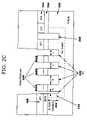
- FIG. 1Ais a cross-sectional schematic diagram of a partially completed SOI structure
- FIG. 1Bis a top-view schematic diagram of the mask shown in FIG. 1A ;
- FIGS. 2A–2Care cross-sectional schematic diagrams of a partially completed SOI structure
- FIGS. 3A–3Care cross-sectional schematic diagrams of a partially completed SOI structure
- FIG. 4is a cross-sectional schematic diagram of a partially completed SOI structure
- FIGS. 5A–5Bare cross-sectional schematic diagrams of a partially completed SOI structure
- FIG. 6is a cross-sectional schematic diagram of a partially completed SOI structure
- FIG. 7is a cross-sectional schematic diagram of a partially completed SOI structure
- FIG. 8is a cross-sectional schematic diagram of a partially completed SOI structure
- FIG. 9is a cross-sectional schematic diagram of a partially completed SOI structure.
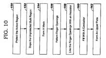
- FIG. 10is a flow diagram illustrating one embodiment of the invention.
- the present inventionprovides integrated high capacitance structures in the SOI bulk region of an SOI semiconductor structure.
- the inventionallows the capacitor plate contacts to be connected through or to the active SOI region, thus affording standard metal processing to enable the use of the capacitor.
- the inventionpositions the capacitive elements completely in the bulk region so as to not have influence to or from the active Si layer.
- the capacitorcan utilize the standard SOI device gate oxide of the transistors that are formed in the active region or a can have unique (thicker or thinner) decoupling capacitor oxide.
- the capacitorcan be fabricated using standard photolithography, or the capacitor can be fabricated using self-assembled minimum feature structures (e.g., nano-structures).
- the inventionprovides an arial density of given capacitance.
- the inventionuses an implant 110 (e.g., N-type implant) made through a mask 100 to form the capacitor plate 112 in the bulk silicon region 106 (e.g., P-type bulk silicon), as shown in FIG. 1A .
- the n-wellcould have N+ concentrations>519/cm3 implanted in the P-type bulk silicon region 106 .
- This bottom plate 112provides a low resistance contact that otherwise could not be formed, for example, in the thin active silicon region.
- Item 108represents the shallow trench isolation (STI) region and item 102 represents the remaining silicon layer that is co-planar with the STI region 108 .
- Item 104is the buried oxide (BOX) layer that creates the silicon-on-insulator (SOI) structure shown in the drawings.
- BOXburied oxide
- the mask 100has openings (regions 1 – 4 in FIG. 1B ) where the implant 110 will be made. These regions 1 – 4 are the bulk silicon areas of the chip that are used primarily for structural support and do not contain active switching devices. The remaining areas of the chip covered by the mask 100 are the active areas of the chip. Normally, no structures are formed in the non-active bulk silicon regions 1 – 4 . However, the invention uses the otherwise unused regions 1 – 4 for the decoupling capacitors. Regions 1 to 4 are arbitrarily chosen for illustration, and could be located in other regions of the chip, and there could be more than (or less than) four distinct regions. In FIG.
- the photoresist mask 100has unprotected regions 1 – 4 where the chip area is open for implantation.
- Regions 1 , and 2may be, for example, the I/O and power supply distributions where the capacitor serves in the capacity of decoupling, region 3 may be a memory region wherein the capacitor now serves a storage element, and region 4 may be the Phase Lock Loop Region, where again the capacitor serves in the capacity of decoupling.
- the capacitorsare located in the normally non-active, bulk silicon areas of the chip.
- the mask 100is not needed, i.e., the implant could be uniform, and through either the shallow trench isolation/BOX regions 108 , 104 , or through the SI/BOX regions 102 , 104 . In this situation, the mask 100 is not used to regionalize the plate implant 112 , and the plate implant 110 will be common, in the entire bulk region. If this alternative is chosen, then the capacitors would serve as one function, i.e., used either as decoupling, or as a memory storage element. We note for chips with multiple power supplies that the mask 100 is very desirable to allow for an independent plate so as to decouple each power supply uniquely, and not to run into a cross talk situation between (for example) noisy supplies where charge could be transferred from one supply to the next.
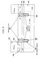
- a photoresist mask 208is used in any common material removal process (such as etching) to form openings for the interdigitated decoupling capacitor (DC) 200 , the plate contact 202 , and the BI contact 206 .
- BIis a common SOI process module where one makes a contact to the bulk region to hold it to a given potential (usually ground) to avoid unwanted potentials on the bulk that may interfere with the BOX and ultimately the active SOI layer by backgating.
- One feature of mask 208is that it can be used to simultaneously make the N+ plate contacts 202 as shown, a BI contact to the P ⁇ Bulk layer 206 , and also the source drain contacts above on the active SOI layer.
- This mask 208is intended to replace the conventional BI mask.
- the formation of the mask imagemay employ dual tone resist so as to fabricate sub-minimum openings for the interdigitated finger of the decoupling capacitor 200 .
- This material removal processcan be performed in stages. For example, the Shallow Trench Isolation (STI) regions 108 and the Buried Oxide region (BOX) 104 can be etched first, and then the openings in the Bulk Silicon region 106 is etched an appropriate distance 204 to ultimately form the structure shown in FIG. 2A .
- STIShallow Trench Isolation
- BOXBuried Oxide region
- FIG. 2Ban alternate approach is used.
- a mask 210is deployed as shown to etch the plate contact 202 .
- a second mask 212 as seen in FIG. 2Cis used to open the capacitor area where the interdigitated trenches are to be etched and protect the remaining areas.
- Self-assembled nanoparticles 206are deposited, and a capacitance density that is much greater than a standard photolithographic density is achieved. After the nanoparticles are formed on the STI 108 , the same etching processes are used to form the finger openings for the decoupling capacitor 200 , as shown in FIG. 2C .
- nanoparticle self-assembly 206will guarantee a defined capacitance, but the interdigitated trench pitch as designated by the trench to trench distances a, b, and c will vary.
- the same etching processesare used to form the finger openings for the decoupling capacitor 200 , as shown in FIG. 2C .
- the decoupling capacitor oxide 302(Decap Oxide) is formed, using any common oxidation of silicon process or insulator deposition process. As shown in FIG. 3A , the oxide 302 can be grown in all trenches, both for the plate contact 202 and for the decoupling capacitor 200 , as well as for such structures as gate oxides in the active areas 315 where transistors 310 will eventually be formed.
- the heavy vertical dashed lineseparates the active area 315 from the bulk silicon region 106 in the drawings. Note that the drawings illustrate a transistor 310 directly adjacent to the bulk silicon region 106 ; however, this is merely for illustration purposes and to distinguish the active area 315 from the bulk silicon 106 , and many designs would not place transistors in this position.
- the mask 300is used to protect areas where a planar capacitor could be formed in region 104 .
- the area used for a fingered capacitoris substantially less than what would be required for a planar capacitor in the same region.
- the same argumentstands for a MIM capacitor that could be formed in the metal layers that subsequently follow above layer 104 . In this case the MIM capacitor would significantly reduce the space available for wiring tracks.
- the insulator 302 within the capacitive fingerscan be formed separately from the insulator 312 of gate oxides in the active area and the lining for the plate contact 202 , which allows the insulators 302 , 312 to be made of different materials and of different thicknesses.
- a mask 304can be used to block oxide growth 302 in the opening for the plate contact and over the SOI active region 315 .
- another mask 306protects the openings for the fingers of the decoupling capacitor 200 and the plated contact 202 opening, while the second insulator 312 is formed as the gate oxide of the transistor 310 .
- the second insulator 312could be formed before the first insulator 302 .
- the first insulator 302could be formed in all regions and then selectively removed (using, for example, mask 306 ) from regions where the second insulator 312 is to be formed.
- one insulatorcould be formed in all regions and then additional insulator thickness could be formed in selected regions (using, for example, mask 304 ) to provide different insulator thicknesses.
- the decap oxide 302will normally be made thicker (but there is no reason why it could not be made thinner) than the thickest gate oxide 312 in the active area so that the oxide 302 can handle power supply variation without degrading. This also eliminates DC tunneling currents (which is a significant and unwanted power draw in the 130 and 90 nm and beyond nodes).
- the openingsare filled with a conductor 400 , such as an in-situ doped n+ polysilicon, intrinsic polysilicon that is later n+ doped through ion implantation, a metal such as tungsten, or an alloy.
- a conductor 400such as an in-situ doped n+ polysilicon, intrinsic polysilicon that is later n+ doped through ion implantation, a metal such as tungsten, or an alloy.
- tungstenor polysilicon, etc.
- Standard contacts (CA/MC) 402 , 404 and subsequent interconnects that integrate the capacitor into the back end wiringare then formed using well-known processing techniques.
- the capacitor areais enhanced by the fingers, and use of the interdigitated fingers reduces the overall area that is required, especially when compared to a planar capacitor or a MiMcap.
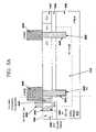
- FIG. 5AShown in FIG. 5A is an e-DRAM implementation where the decoupling capacitor is now used as a DRAM storage element. It is assumed for simplicity of illustration that, in the e-DRAM environment, only one interdigitated capacitor per transfer device would be required. However, one ordinarily skilled in the art would understand that each transistor could be connected to multiple fingers of a multiple finger decoupling capacitor.
- Item 500represents the gate (N+ word line) and items 502 , 504 represent the node and bitline connection of the transistor. Therefore, item 504 is shown as the N+ bit line and item 502 is shown as the node of the transistor that is connected to the capacitor 200 through the contact 402 which acts as a strap.
- FIG. 5Ashows an alternate embodiment where the node diffusion 502 is merged with the capacitor 200 inner plate.
- FIG. 5Bsaves space in the design of the cell.
- FIGS. 6–9illustrate a sequence of additional processing steps used to fabricate the DRAM cell capacitor as shown in FIG. 5A or 5 B, and for completing the decoupling capacitors as depicted in FIG. 4 , when a DRAM cell is required in addition to a decoupling capacitor.
- a multi-finger capacitorcould be used as an alternative. Even in the case of a single finger, significant DRAM cell area advantages exist when contrasted to the formation of a planar DRAM capacitor, amortized for example over a typical array on the order of one to six megabytes.
- a DRAM and/or decoupling capacitor dielectric 604is grown in regions that are opened by a photoresist mask 600 .
- the di-electric 604grows on the sidewall of the exposed silicon island 602 .
- This growth of the silicon island 602is undesirable and will be removed as shown below.
- a partial fill and etch back of a conductor 700e.g., N+ in-situ doped or intrinsic polysilicon
- BOX region 104As BOX regions are typically on the order of the silicon thickness, i.e., 300–800 angstroms, such a process step is not critical. As shown in FIG.
- a second polysilicon top fill 900is used to complete both the e-Dram capacitor, the trench plate connections (for decoupling capacitors and the e-Dram cell), and the decoupling capacitor top fill. Note that the top fill will be a bit wider than the bottom fill by the width of the dielectric etch (this is overexagerrated in FIG. 9 ).
- the inventionforms a silicon-on-insulator integrated structure, that comprises at least one active region comprising active devices, and at least one bulk region adapted to provide structural support to the active region.
- the inventionfirst protects the active region with a first mask 150 and dopes the unprotected bulk region 152 to form a common lower plate.
- the lower platemay or may not be in common.
- the lower plateIn a power supply system with decoupling capacitors, the lower plate can be common, but it does not have to be (i.e., if the decoupling capacitors fail, it may be desirable to have the option to isolate them for example with e-fuses).
- the lower plateswould not be in common and different capacitor designs could be used for different power supply designs within the same chip.
- the inventionthen forms a second mask used to pattern the capacitive fingers 154 .
- This second maskcan be a conventional photolithographic mask or can be formed by depositing self-assembling nanoparticles on the bulk region as the second mask.
- the finger openingsare patterned 156 (e.g., by etching, etc.) into the bulk region through the second mask.
- the finger openingsare then lined with an insulator 158 and filled with a conductor 160 to form the capacitive fingers that extend into the bulk region.
- These capacitive fingersextend vertically into the bulk region, in a direction perpendicular to the horizontal upper surface of the bulk region.
- the insulator within the capacitive fingerscan be formed separately from gate insulators of transistors in the active area, which allows the insulator to be made of a different material and of a different thickness than the gate insulators.
- an upper plateis formed 162 .
- the upper plateis only common within the supply or Dram Cell that it is connecting to.
- the upper plateis connected to the conductors within the capacitive fingers and can be formed to extend from the decoupling capacitor into the active region.
- the decoupling capacitorcan be connected to a transistor such that the decoupling capacitor comprises a storage element of a dynamic random access memory (DRAM) memory element.
- DRAMdynamic random access memory
- the present inventionprovides integrated high capacitance structures in the SOI bulk region of an SOI semiconductor structure.
- the inventionallows the capacitor plate contacts to be connected through or to the active SOI region, thus affording standard metal processing to enable the use of the capacitor.
- the inventionpositions the capacitive elements completely in the bulk region so as to not have influence to or from the active Si layer.
- the capacitorcan utilize the standard SOI device gate oxide of the transistors that are formed in the active region or a can have unique (thicker or thinner) decoupling capacitor oxide.
- the capacitorcan be fabricated using standard photolithography, or the capacitor can be fabricated using self-assembled minimum feature structures (e.g., nano-structures).
- the inventionprovides an arial density of given capacitance.
Landscapes
- Engineering & Computer Science (AREA)
- Manufacturing & Machinery (AREA)
- Semiconductor Integrated Circuits (AREA)
- Semiconductor Memories (AREA)
Abstract
Description
Claims (18)
Priority Applications (2)
| Application Number | Priority Date | Filing Date | Title |
|---|---|---|---|
| US10/710,256US7102204B2 (en) | 2004-06-29 | 2004-06-29 | Integrated SOI fingered decoupling capacitor |
| US11/485,599US7674675B2 (en) | 2004-06-29 | 2006-07-12 | Method of forming an integrated SOI fingered decoupling capacitor |
Applications Claiming Priority (1)
| Application Number | Priority Date | Filing Date | Title |
|---|---|---|---|
| US10/710,256US7102204B2 (en) | 2004-06-29 | 2004-06-29 | Integrated SOI fingered decoupling capacitor |
Related Child Applications (1)
| Application Number | Title | Priority Date | Filing Date |
|---|---|---|---|
| US11/485,599DivisionUS7674675B2 (en) | 2004-06-29 | 2006-07-12 | Method of forming an integrated SOI fingered decoupling capacitor |
Publications (2)
| Publication Number | Publication Date |
|---|---|
| US20050287718A1 US20050287718A1 (en) | 2005-12-29 |
| US7102204B2true US7102204B2 (en) | 2006-09-05 |
Family
ID=35506395
Family Applications (2)
| Application Number | Title | Priority Date | Filing Date |
|---|---|---|---|
| US10/710,256Expired - LifetimeUS7102204B2 (en) | 2004-06-29 | 2004-06-29 | Integrated SOI fingered decoupling capacitor |
| US11/485,599Expired - Fee RelatedUS7674675B2 (en) | 2004-06-29 | 2006-07-12 | Method of forming an integrated SOI fingered decoupling capacitor |
Family Applications After (1)
| Application Number | Title | Priority Date | Filing Date |
|---|---|---|---|
| US11/485,599Expired - Fee RelatedUS7674675B2 (en) | 2004-06-29 | 2006-07-12 | Method of forming an integrated SOI fingered decoupling capacitor |
Country Status (1)
| Country | Link |
|---|---|
| US (2) | US7102204B2 (en) |
Cited By (12)
| Publication number | Priority date | Publication date | Assignee | Title |
|---|---|---|---|---|
| US20060109464A1 (en)* | 2004-11-22 | 2006-05-25 | Akiyuki Minami | Method for detecting alignment accuracy |
| US20060197154A1 (en)* | 2005-03-03 | 2006-09-07 | Advanced Micro Devices, Inc. | Semiconductor component and method of manufacture |
| US20070102769A1 (en)* | 2005-11-08 | 2007-05-10 | Taiwan Semiconductor Manufacturing Company, Ltd. | Dual SOI structure |
| US20090236691A1 (en)* | 2008-03-24 | 2009-09-24 | International Business Machines Corporation | Deep trench (dt) metal-insulator-metal (mim) capacitor |
| US20090242952A1 (en)* | 2008-03-27 | 2009-10-01 | Qimonda Ag | Integrated circuit including a capacitor and method |
| US20110049673A1 (en)* | 2009-08-26 | 2011-03-03 | International Business Machines Corporation | Nanopillar Decoupling Capacitor |
| US20110175152A1 (en)* | 2010-01-19 | 2011-07-21 | International Business Machines Corporation | Method and structure for forming high performance mos capacitor along with fully depleted semiconductor on insulator devices on the same chip |
| US8117581B1 (en)* | 2006-06-07 | 2012-02-14 | Oracle America, Inc. | Self-propelling decoupling capacitor design for flexible area decoupling capacitor fill design flow |
| US8507354B2 (en) | 2011-12-08 | 2013-08-13 | International Business Machines Corporation | On-chip capacitors in combination with CMOS devices on extremely thin semiconductor on insulator (ETSOI) substrates |
| US20140124845A1 (en)* | 2011-12-12 | 2014-05-08 | International Business Machines Corporation | Method and Structure for Forming On-Chip High Quality Capacitors With ETSOI Transistors |
| US9818652B1 (en)* | 2016-04-27 | 2017-11-14 | Globalfoundries Inc. | Commonly-bodied field-effect transistors |
| US12057387B2 (en) | 2020-12-03 | 2024-08-06 | International Business Machines Corporation | Decoupling capacitor inside gate cut trench |
Families Citing this family (10)
| Publication number | Priority date | Publication date | Assignee | Title |
|---|---|---|---|---|
| KR100684433B1 (en)* | 2004-12-22 | 2007-02-16 | 동부일렉트로닉스 주식회사 | Method of manufacturing metal-insulator-metal capacitor |
| EP1691415A1 (en)* | 2005-02-14 | 2006-08-16 | Seiko Epson Corporation | Semiconductor device with implanted passive elements |
| US7439127B2 (en)* | 2006-04-20 | 2008-10-21 | Advanced Micro Devices, Inc. | Method for fabricating a semiconductor component including a high capacitance per unit area capacitor |
| US8080851B2 (en)* | 2008-08-29 | 2011-12-20 | International Business Machines Corporation | Deep trench electrostatic discharge (ESD) protect diode for silicon-on-insulator (SOI) devices |
| US8232162B2 (en) | 2010-09-13 | 2012-07-31 | International Business Machines Corporation | Forming implanted plates for high aspect ratio trenches using staged sacrificial layer removal |
| US8569816B2 (en)* | 2011-04-21 | 2013-10-29 | Freescale Semiconductor, Inc. | Isolated capacitors within shallow trench isolation |
| US8642423B2 (en)* | 2011-11-30 | 2014-02-04 | International Business Machines Corporation | Polysilicon/metal contact resistance in deep trench |
| US9472512B1 (en)* | 2015-10-14 | 2016-10-18 | Globalfoundries Singapore Pte. Ltd. | Integrated circuits with contacts through a buried oxide layer and methods of producing the same |
| US10090378B1 (en) | 2017-03-17 | 2018-10-02 | International Business Machines Corporation | Efficient metal-insulator-metal capacitor |
| US10847508B2 (en)* | 2018-12-27 | 2020-11-24 | Micron Technology, Inc. | Apparatus with a current-gain layout |
Citations (17)
| Publication number | Priority date | Publication date | Assignee | Title |
|---|---|---|---|---|
| US5206787A (en) | 1991-04-01 | 1993-04-27 | Fujitsu Limited | Capacitor and method of fabricating same |
| US5304506A (en) | 1993-03-10 | 1994-04-19 | Micron Semiconductor, Inc. | On chip decoupling capacitor |
| US5661340A (en) | 1991-07-25 | 1997-08-26 | Fujitsu Limited | Dynamic random access memory having a stacked fin capacitor with reduced fin thickness |
| US5688709A (en) | 1996-02-14 | 1997-11-18 | Lsi Logic Corporation | Method for forming composite trench-fin capacitors for DRAMS |
| US5759907A (en)* | 1996-09-16 | 1998-06-02 | International Business Machines Corporation | Method of making large value capacitor for SOI |
| US5789289A (en) | 1996-06-18 | 1998-08-04 | Vanguard International Semiconductor Corporation | Method for fabricating vertical fin capacitor structures |
| US5872697A (en) | 1996-02-13 | 1999-02-16 | International Business Machines Corporation | Integrated circuit having integral decoupling capacitor |
| US6015729A (en) | 1995-10-06 | 2000-01-18 | Micron Technology, Inc. | Integrated chip multilayer decoupling capcitors |
| US6096584A (en) | 1997-03-05 | 2000-08-01 | International Business Machines Corporation | Silicon-on-insulator and CMOS-on-SOI double film fabrication process with a coplanar silicon and isolation layer and adding a second silicon layer on one region |
| US6188122B1 (en)* | 1999-01-14 | 2001-02-13 | International Business Machines Corporation | Buried capacitor for silicon-on-insulator structure |
| US20020036322A1 (en)* | 2000-03-17 | 2002-03-28 | Ramachandra Divakauni | SOI stacked dram logic |
| US20020064913A1 (en)* | 2000-10-12 | 2002-05-30 | Adkisson James W. | Embedded dram on silicon-on-insulator substrate |
| US6475838B1 (en) | 2000-03-14 | 2002-11-05 | International Business Machines Corporation | Methods for forming decoupling capacitors |
| US6492244B1 (en) | 2001-11-21 | 2002-12-10 | International Business Machines Corporation | Method and semiconductor structure for implementing buried dual rail power distribution and integrated decoupling capacitance for silicon on insulator (SOI) devices |
| US6552381B2 (en)* | 2000-04-25 | 2003-04-22 | Agere Systems, Inc. | Trench capacitors in SOI substrates |
| US6608365B1 (en)* | 2002-06-04 | 2003-08-19 | Lsi Logic Corporation | Low leakage PMOS on-chip decoupling capacitor cells compatible with standard CMOS cells |
| US6963483B2 (en)* | 1999-12-29 | 2005-11-08 | Intel Corporation | Self-aligned coaxial via capacitors |
Family Cites Families (4)
| Publication number | Priority date | Publication date | Assignee | Title |
|---|---|---|---|---|
| US4983544A (en)* | 1986-10-20 | 1991-01-08 | International Business Machines Corporation | Silicide bridge contact process |
| TW452852B (en)* | 2000-05-31 | 2001-09-01 | Nanya Technology Corp | Method of improving the degree of flatness of resist layer |
| US6566191B2 (en)* | 2000-12-05 | 2003-05-20 | International Business Machines Corporation | Forming electronic structures having dual dielectric thicknesses and the structure so formed |
| US20030116531A1 (en)* | 2001-12-20 | 2003-06-26 | Kamins Theodore I. | Method of forming one or more nanopores for aligning molecules for molecular electronics |
- 2004
- 2004-06-29USUS10/710,256patent/US7102204B2/ennot_activeExpired - Lifetime
- 2006
- 2006-07-12USUS11/485,599patent/US7674675B2/ennot_activeExpired - Fee Related
Patent Citations (23)
| Publication number | Priority date | Publication date | Assignee | Title |
|---|---|---|---|---|
| US5206787A (en) | 1991-04-01 | 1993-04-27 | Fujitsu Limited | Capacitor and method of fabricating same |
| US5661340A (en) | 1991-07-25 | 1997-08-26 | Fujitsu Limited | Dynamic random access memory having a stacked fin capacitor with reduced fin thickness |
| US5304506A (en) | 1993-03-10 | 1994-04-19 | Micron Semiconductor, Inc. | On chip decoupling capacitor |
| US6015729A (en) | 1995-10-06 | 2000-01-18 | Micron Technology, Inc. | Integrated chip multilayer decoupling capcitors |
| US6124163A (en) | 1995-10-06 | 2000-09-26 | Micron Technology, Inc. | Integrated chip multiplayer decoupling capacitors |
| US6303457B1 (en) | 1996-02-13 | 2001-10-16 | Todd Alan Christensen | Integrated circuit having integral decoupling capacitor |
| US5872697A (en) | 1996-02-13 | 1999-02-16 | International Business Machines Corporation | Integrated circuit having integral decoupling capacitor |
| US5688709A (en) | 1996-02-14 | 1997-11-18 | Lsi Logic Corporation | Method for forming composite trench-fin capacitors for DRAMS |
| US6081008A (en) | 1996-02-14 | 2000-06-27 | Lsi Logic Corporation | Composite trench-fin capacitors for DRAM |
| US5789289A (en) | 1996-06-18 | 1998-08-04 | Vanguard International Semiconductor Corporation | Method for fabricating vertical fin capacitor structures |
| US5759907A (en)* | 1996-09-16 | 1998-06-02 | International Business Machines Corporation | Method of making large value capacitor for SOI |
| US5770875A (en) | 1996-09-16 | 1998-06-23 | International Business Machines Corporation | Large value capacitor for SOI |
| US6096584A (en) | 1997-03-05 | 2000-08-01 | International Business Machines Corporation | Silicon-on-insulator and CMOS-on-SOI double film fabrication process with a coplanar silicon and isolation layer and adding a second silicon layer on one region |
| US6188122B1 (en)* | 1999-01-14 | 2001-02-13 | International Business Machines Corporation | Buried capacitor for silicon-on-insulator structure |
| US6337253B1 (en) | 1999-01-14 | 2002-01-08 | International Business Machines Corporation | Process of making buried capacitor for silicon-on-insulator structure |
| US6963483B2 (en)* | 1999-12-29 | 2005-11-08 | Intel Corporation | Self-aligned coaxial via capacitors |
| US6475838B1 (en) | 2000-03-14 | 2002-11-05 | International Business Machines Corporation | Methods for forming decoupling capacitors |
| US20020036322A1 (en)* | 2000-03-17 | 2002-03-28 | Ramachandra Divakauni | SOI stacked dram logic |
| US6552381B2 (en)* | 2000-04-25 | 2003-04-22 | Agere Systems, Inc. | Trench capacitors in SOI substrates |
| US20020064913A1 (en)* | 2000-10-12 | 2002-05-30 | Adkisson James W. | Embedded dram on silicon-on-insulator substrate |
| US6492244B1 (en) | 2001-11-21 | 2002-12-10 | International Business Machines Corporation | Method and semiconductor structure for implementing buried dual rail power distribution and integrated decoupling capacitance for silicon on insulator (SOI) devices |
| US20030094654A1 (en)* | 2001-11-21 | 2003-05-22 | International Business Machines Corporation | Method and semiconductor structure for implementing buried dual rail power distribution and integrated decoupling capacitance for silicon on insulator (SOI) devices |
| US6608365B1 (en)* | 2002-06-04 | 2003-08-19 | Lsi Logic Corporation | Low leakage PMOS on-chip decoupling capacitor cells compatible with standard CMOS cells |
Cited By (24)
| Publication number | Priority date | Publication date | Assignee | Title |
|---|---|---|---|---|
| US20060109464A1 (en)* | 2004-11-22 | 2006-05-25 | Akiyuki Minami | Method for detecting alignment accuracy |
| US20060197154A1 (en)* | 2005-03-03 | 2006-09-07 | Advanced Micro Devices, Inc. | Semiconductor component and method of manufacture |
| US7223640B2 (en)* | 2005-03-03 | 2007-05-29 | Advanced Micro Devices, Inc. | Semiconductor component and method of manufacture |
| US7986029B2 (en)* | 2005-11-08 | 2011-07-26 | Taiwan Semiconductor Manufacturing Company, Ltd. | Dual SOI structure |
| US20070102769A1 (en)* | 2005-11-08 | 2007-05-10 | Taiwan Semiconductor Manufacturing Company, Ltd. | Dual SOI structure |
| US8117581B1 (en)* | 2006-06-07 | 2012-02-14 | Oracle America, Inc. | Self-propelling decoupling capacitor design for flexible area decoupling capacitor fill design flow |
| US20090236691A1 (en)* | 2008-03-24 | 2009-09-24 | International Business Machines Corporation | Deep trench (dt) metal-insulator-metal (mim) capacitor |
| US7741188B2 (en)* | 2008-03-24 | 2010-06-22 | International Business Machines Corporation | Deep trench (DT) metal-insulator-metal (MIM) capacitor |
| US20090242952A1 (en)* | 2008-03-27 | 2009-10-01 | Qimonda Ag | Integrated circuit including a capacitor and method |
| US7880269B2 (en) | 2008-03-27 | 2011-02-01 | Qimonda Ag | Integrated circuit including a capacitor and method |
| US8258037B2 (en) | 2009-08-26 | 2012-09-04 | International Business Machines Corporation | Nanopillar decoupling capacitor |
| US8680651B2 (en) | 2009-08-26 | 2014-03-25 | International Business Machines Corporation | Nanopillar decoupling capacitor |
| US20110049673A1 (en)* | 2009-08-26 | 2011-03-03 | International Business Machines Corporation | Nanopillar Decoupling Capacitor |
| US20110175152A1 (en)* | 2010-01-19 | 2011-07-21 | International Business Machines Corporation | Method and structure for forming high performance mos capacitor along with fully depleted semiconductor on insulator devices on the same chip |
| US8513723B2 (en) | 2010-01-19 | 2013-08-20 | International Business Machines Corporation | Method and structure for forming high performance MOS capacitor along with fully depleted semiconductor on insulator devices on the same chip |
| US8921908B2 (en) | 2011-12-08 | 2014-12-30 | International Business Machines Corporation | On-chip capacitors in combination with CMOS devices on extremely thin semiconductor on insulator (ETSOI) substrates |
| US8507354B2 (en) | 2011-12-08 | 2013-08-13 | International Business Machines Corporation | On-chip capacitors in combination with CMOS devices on extremely thin semiconductor on insulator (ETSOI) substrates |
| US20140124845A1 (en)* | 2011-12-12 | 2014-05-08 | International Business Machines Corporation | Method and Structure for Forming On-Chip High Quality Capacitors With ETSOI Transistors |
| US8969938B2 (en)* | 2011-12-12 | 2015-03-03 | International Business Machines Corporation | Method and structure for forming on-chip high quality capacitors with ETSOI transistors |
| DE112012005166B4 (en) | 2011-12-12 | 2020-06-04 | Globalfoundries Inc. | Method and structure for forming high quality on-chip capacitors with ETSOI transistors |
| US9818652B1 (en)* | 2016-04-27 | 2017-11-14 | Globalfoundries Inc. | Commonly-bodied field-effect transistors |
| CN107359167A (en)* | 2016-04-27 | 2017-11-17 | 格罗方德半导体公司 | Ontological field-effect transistor altogether |
| CN107359167B (en)* | 2016-04-27 | 2020-08-14 | 格罗方德半导体公司 | Common Ontology Field Effect Transistor |
| US12057387B2 (en) | 2020-12-03 | 2024-08-06 | International Business Machines Corporation | Decoupling capacitor inside gate cut trench |
Also Published As
| Publication number | Publication date |
|---|---|
| US7674675B2 (en) | 2010-03-09 |
| US20060252226A1 (en) | 2006-11-09 |
| US20050287718A1 (en) | 2005-12-29 |
Similar Documents
| Publication | Publication Date | Title |
|---|---|---|
| US7674675B2 (en) | Method of forming an integrated SOI fingered decoupling capacitor | |
| JP3161354B2 (en) | Semiconductor device and manufacturing method thereof | |
| US7999297B2 (en) | Semiconductor device having stacked decoupling capacitors | |
| US20230013420A1 (en) | Semiconductor structure and fabrication method thereof | |
| US20070134819A1 (en) | Semiconductor device and method of manufacturing the same | |
| US20090087958A1 (en) | Semiconductor device and manufacturing method thereof | |
| US9041154B2 (en) | Contact structure and semiconductor memory device using the same | |
| JPH05251657A (en) | Semiconductor memory cell and its manufacture | |
| US20230276617A1 (en) | Semiconductor structure and fabrication method therefor | |
| WO2019236149A1 (en) | Integrated assemblies having dielectric regions along conductive structures, and methods of forming integrated assemblies | |
| CN114242675A (en) | Semiconductor element with composite bonding pad | |
| US9871096B2 (en) | Serial capacitor device with middle electrode contact | |
| US8809149B2 (en) | High density serial capacitor device and methods of making such a capacitor device | |
| US20060197135A1 (en) | Semiconductor device having a cylindrical capacitor element | |
| US11637105B2 (en) | Apparatus comprising compensation capacitors | |
| US20240038904A1 (en) | Apparatuses including capacitors including multiple dielectric materials | |
| JP2917912B2 (en) | Semiconductor memory device and method of manufacturing the same | |
| US7101768B2 (en) | Self-aligned selective hemispherical grain deposition process and structure for enhanced capacitance trench capacitor | |
| US8283713B2 (en) | Logic-based eDRAM using local interconnects to reduce impact of extension contact parasitics | |
| US20050079679A1 (en) | Trench capacitor and method for fabricating a trench capacitor | |
| US20110092036A1 (en) | Method for manufacturing semiconductor device | |
| US12193222B2 (en) | Semiconductor structure and method for forming semiconductor structure | |
| JP2748867B2 (en) | Semiconductor storage device | |
| CN120786875A (en) | Memory device, semiconductor structure and manufacturing method thereof | |
| CN114188272A (en) | Manufacturing method of semiconductor element |
Legal Events
| Date | Code | Title | Description |
|---|---|---|---|
| AS | Assignment | Owner name:INTERNATIONAL BUSINESS MACHINES CORPORATION, NEW Y Free format text:ASSIGNMENT OF ASSIGNORS INTEREST;ASSIGNORS:BERDLMAIER, ZACHERY E.;KIEWRA, EDWARD W.;TONTI, WILLIAM R.;AND OTHERS;REEL/FRAME:014791/0923;SIGNING DATES FROM 20040622 TO 20040629 | |
| AS | Assignment | Owner name:INTERNATIONAL BUSINESS MACHINES CORPORATION, NEW Y Free format text:CORRECTIVE ASSIGNMENT TO CORRECT THE NAME OF THE FIRST ASSIGNOR. DOCUMENT PREVIOUSLY RECORDED AT REEL 014791 FRAME 0923;ASSIGNORS:BERNDLMAIER, ZACHARY E.;KIEWRA, EDWARD W.;TONTI, WILLIAM R.;AND OTHERS;REEL/FRAME:015333/0091;SIGNING DATES FROM 20040622 TO 20040629 | |
| FEPP | Fee payment procedure | Free format text:PAYOR NUMBER ASSIGNED (ORIGINAL EVENT CODE: ASPN); ENTITY STATUS OF PATENT OWNER: LARGE ENTITY | |
| STCF | Information on status: patent grant | Free format text:PATENTED CASE | |
| FPAY | Fee payment | Year of fee payment:4 | |
| REMI | Maintenance fee reminder mailed | ||
| FPAY | Fee payment | Year of fee payment:8 | |
| SULP | Surcharge for late payment | Year of fee payment:7 | |
| AS | Assignment | Owner name:GLOBALFOUNDRIES U.S. 2 LLC, NEW YORK Free format text:ASSIGNMENT OF ASSIGNORS INTEREST;ASSIGNOR:INTERNATIONAL BUSINESS MACHINES CORPORATION;REEL/FRAME:036550/0001 Effective date:20150629 | |
| AS | Assignment | Owner name:GLOBALFOUNDRIES INC., CAYMAN ISLANDS Free format text:ASSIGNMENT OF ASSIGNORS INTEREST;ASSIGNORS:GLOBALFOUNDRIES U.S. 2 LLC;GLOBALFOUNDRIES U.S. INC.;REEL/FRAME:036779/0001 Effective date:20150910 | |
| MAFP | Maintenance fee payment | Free format text:PAYMENT OF MAINTENANCE FEE, 12TH YEAR, LARGE ENTITY (ORIGINAL EVENT CODE: M1553) Year of fee payment:12 | |
| AS | Assignment | Owner name:WILMINGTON TRUST, NATIONAL ASSOCIATION, DELAWARE Free format text:SECURITY AGREEMENT;ASSIGNOR:GLOBALFOUNDRIES INC.;REEL/FRAME:049490/0001 Effective date:20181127 | |
| AS | Assignment | Owner name:GLOBALFOUNDRIES U.S. INC., CALIFORNIA Free format text:ASSIGNMENT OF ASSIGNORS INTEREST;ASSIGNOR:GLOBALFOUNDRIES INC.;REEL/FRAME:054633/0001 Effective date:20201022 | |
| AS | Assignment | Owner name:GLOBALFOUNDRIES INC., CAYMAN ISLANDS Free format text:RELEASE BY SECURED PARTY;ASSIGNOR:WILMINGTON TRUST, NATIONAL ASSOCIATION;REEL/FRAME:054636/0001 Effective date:20201117 | |
| AS | Assignment | Owner name:GLOBALFOUNDRIES U.S. INC., NEW YORK Free format text:RELEASE BY SECURED PARTY;ASSIGNOR:WILMINGTON TRUST, NATIONAL ASSOCIATION;REEL/FRAME:056987/0001 Effective date:20201117 |