US7099980B1 - Data storage system having port disable mechanism - Google Patents
Data storage system having port disable mechanismDownload PDFInfo
- Publication number
- US7099980B1 US7099980B1US10/740,220US74022003AUS7099980B1US 7099980 B1US7099980 B1US 7099980B1US 74022003 AUS74022003 AUS 74022003AUS 7099980 B1US7099980 B1US 7099980B1
- Authority
- US
- United States
- Prior art keywords
- director
- memory
- board
- boards
- transmit
- Prior art date
- Legal status (The legal status is an assumption and is not a legal conclusion. Google has not performed a legal analysis and makes no representation as to the accuracy of the status listed.)
- Expired - Lifetime, expires
Links
Images


Classifications
- G—PHYSICS
- G11—INFORMATION STORAGE
- G11B—INFORMATION STORAGE BASED ON RELATIVE MOVEMENT BETWEEN RECORD CARRIER AND TRANSDUCER
- G11B33/00—Constructional parts, details or accessories not provided for in the other groups of this subclass
- G11B33/12—Disposition of constructional parts in the apparatus, e.g. of power supply, of modules
- G—PHYSICS
- G06—COMPUTING OR CALCULATING; COUNTING
- G06F—ELECTRIC DIGITAL DATA PROCESSING
- G06F3/00—Input arrangements for transferring data to be processed into a form capable of being handled by the computer; Output arrangements for transferring data from processing unit to output unit, e.g. interface arrangements
- G06F3/06—Digital input from, or digital output to, record carriers, e.g. RAID, emulated record carriers or networked record carriers
- G06F3/0601—Interfaces specially adapted for storage systems
- G06F3/0668—Interfaces specially adapted for storage systems adopting a particular infrastructure
- G06F3/0671—In-line storage system
- G06F3/0673—Single storage device
Definitions
- This inventionrelates generally to data storage system, and more particularly to data storage systems having director boards and memory boards interconnected through a backplane and for selectively disabling ports on the director boards and memory boards.
- host computer/serversAs is known in the art, large host computers and servers (collectively referred to herein as “host computer/servers”) require large capacity data storage systems. These large computer/servers generally include data processors which perform many operations on data introduced to the host computer/server through peripherals including the data storage system. The results of these operations are output to peripherals, including the storage system.
- One type of data storage systemis a magnetic disk storage system.
- a bank of disk drives and the host computer/serverare coupled together through an interface.
- the interfaceincludes “front end” or host computer/server controllers (or directors) and “back-end” or disk controllers (or directors).
- the interfaceoperates the controllers (or directors) in such a way that they are transparent to the host computer/server. That is, data is stored in, and retrieved from, the bank of disk drives in such a way that the host computer/server merely thinks it is operating with its own local disk drive.
- One such systemis described in U.S. Pat. No.
- the interfacemay also include, in addition to the host computer/server controllers (or directors) and disk controllers (sometimes also referred to as directors), addressable cache memories.
- the cache memoryis a semiconductor memory and is provided to rapidly store data from the host computer/server before storage in the disk drives, and, on the other hand, store data from the disk drives prior to being sent to the host computer/server.
- the cache memorybeing a semiconductor memory, as distinguished from a magnetic memory as in the case of the disk drives, is much faster than the disk drives in reading and writing data.
- the host computer/server controllers, disk controllers and cache memoryare interconnected through a backplane printed circuit board (i.e., backplane). More particularly, disk controllers are mounted on disk controller printed circuit boards.
- the host computer/server controllersare mounted on host computer/server controller printed circuit boards.
- cache memoriesare mounted on cache memory printed circuit boards.
- the disk directors, host computer/server directors, and cache memory printed circuit boardsplug into the backplane.
- a data storage systemfor transferring data between a host computer/server and a bank of disk drives through a system interface.
- the system interfaceincludes a backplane adapted to have plugged therein a plurality of director boards and a plurality of memory boards.
- Each one of such director boardsincludes a plurality of director board transmit/receive units.
- Each one of the director board transmit/receive unitsis associated with a corresponding one of the plurality of memory boards.
- Each one of the director board transmit/receive unitsis adapted to be disabled in the absence of the one of the memory boards associated with such one of the director board transmit/receive units.
- Each one of the memory boardsincludes a plurality of memory board transmit/receive units.
- Each one of the memory board transmit/receive unitsis associated with a corresponding one of the plurality of director boards.
- Each one of the memory board transmit/receive unitsis adapted to be disabled to prevent transmit/receive data therethrough in the absence of the one of such director boards associated with such one of the memory board transmit/receive units.
- FIG. 1is a block diagram of a data storage system according to the invention.
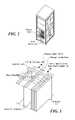
- FIG. 2is a sketch of an electrical cabinet storing a system interface used in the data storage system of FIG. 1 ;
- FIG. 3is a diagramatical, isometric sketch showing printed circuit boards providing the system interface of the data storage system of FIG. 1 ;
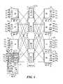
- FIG. 4is a block diagram of the system interface used in the data storage system of FIG. 1 ;
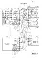
- FIG. 5is a diagram of a system according to the invention, such system having an arrangement of memory boards and director boards interconnected through a backplane and for selectively disabling ports on the director boards and memory boards according to the invention;
- FIG. 5Ais a diagram of the system of FIG. 5 with one of the memory boards absent from the backplane;
- FIG. 5Bis a diagram of the system of FIG. 5 with one of the director boards absent from the backplane.
- the system interface 160includes: a plurality of, here 32 front-end directors 180 1 – 180 32 coupled to the host computer/server 120 via ports 123 1 – 123 32 ; a plurality of back-end directors 200 1 – 200 32 coupled to the bank of disk drives 140 via ports 123 33 – 123 64 ; a data transfer section 240 , having a global cache memory 220 , coupled to the plurality of front-end directors 180 1 – 180 16 and the back-end directors 200 1 – 200 16 ; and a messaging network 260 , operative independently of the data transfer section 240 , coupled to the plurality of front-end directors 180 1 – 180 32 and the plurality of back-end directors 200 1 – 200 32 , as shown.
- the front-end and back-end directors 180 1 – 180 32 , 200 1 – 200 32are functionally similar and include a microprocessor ( ⁇ P) 299 (i.e., a central processing unit (CPU) and RAM), a message engine/CPU controller 314 and a data pipe 316 , described in detail in the co-pending patent applications referred to above. Suffice it to say here, however, that the front-end and back-end directors 180 1 – 180 32 , 200 1 – 200 32 control data transfer between the host computer/server 120 and the bank of disk drives 140 in response to messages passing between the directors 180 1 – 180 32 , 200 1 – 200 32 through the messaging network 260 . The messages facilitate the data transfer between host computer/server 120 and the bank of disk drives 140 with such data passing through the global cache memory 220 via the data transfer section 240 .
- ⁇ Pmicroprocessor
- CPUcentral processing unit
- RAMrandom access memory
- message engine/CPU controller 314i.e., a central processing unit (
- each one of the host computer processors 121 1 – 121 32is coupled to here a pair (but not limited to a pair) of the front-end directors 180 1 – 180 32 , to provide redundancy in the event of a failure in one of the front end-directors 181 1 – 181 32 coupled thereto.
- the bank of disk drives 140has a plurality of, here 32 , disk drives 141 1 – 141 32 , each disk drive 141 1 – 141 32 being coupled to here a pair (but not limited to a pair) of the back-end directors 200 1 – 200 32 , to provide redundancy in the event of a failure in one of the back-end directors 200 1 – 200 32 coupled thereto).
- front-end director pairs 180 1 , 180 2 ; . . . 180 31 , 180 32are coupled to processor pairs 121 1 , 121 2 ; . . . 121 31 , 121 32 , respectively, as shown.
- back-end director pairs 200 1 , 200 2 ; . . . 200 31 , 200 32are coupled to disk drive pairs 141 1 , 141 2 ; . . . 141 31 , 141 32 , respectively, as shown.
- the system interface 160is shown to include an electrical cabinet 300 having stored therein: a plurality of, here eight front-end director boards 190 1 – 190 8 , each one having here four of the front-end directors 180 1 – 180 32 ; a plurality of, here eight back-end director boards 210 1 – 210 8 , each one having here four of the back-end directors 200 1 – 200 32 ; and a plurality of, here eight, memory boards M 0 –M 7 which together make up the global cache memory 220 .
- These boardsplug into the front side of a backplane 302 ( FIG. 3 ) (It is noted that the backplane 302 is a mid-plane printed circuit board).
- Plugged into the backside of the backplane 302are message network boards which together make up the message network 260 as described in the co-pending patent applications referred to above.
- the backside of the backplane 302has plugged into it adapter boards, not shown in FIGS. 2–4 , which couple the boards plugged into the back-side of the backplane 302 with the computer 120 and the bank of disk drives 140 as shown in FIG. 1 .
- an I/O adapteris coupled between each one of the front-end (FE) directors 180 1 – 180 32 and the host computer 120 and an I/O adapter, not shown, is coupled between each one of the back-end (BE) directors 200 1 – 200 32 and the bank of disk drives 140 .
- each one of the director boards 190 1 – 210 8includes, as noted above four of the directors 180 1 – 180 32 , 200 1 – 200 32 ( FIG. 1 ). It is noted that the director boards 190 1 – 190 8 having four front-end directors per board, 180 1 – 180 32 are referred to as front-end directors and the director boards 210 1 – 210 8 having four back-end directors per board, 200 1 – 200 32 are referred to as back-end directors.
- Each one of the directors 180 1 – 180 32 , 200 1 – 200 32includes the microprocessor 299 referred to above, the message engine/CPU controller 314 , and the data pipe 316 shown in FIG. 1 .
- the front-end director boardshave ports 123 1 – 123 32 , as shown in FIG. 1 , coupled to the processors 121 1 – 121 32 , as shown.
- the back-end director boardshave ports 123 33 – 123 64 , as shown in FIG. 2 , coupled to the disk drives 141 1 – 141 32 , as shown.
- Each one of the director boards 190 1 – 210 8includes a crossbar switch 318 as shown in FIG. 4 .
- the crossbar switch 318has eight input/output ports C 1 –C 8 , each one being coupled to the data pipe 316 ( FIG. 1 ) of a corresponding one of the four directors 180 1 – 180 32 , 200 1 – 200 32 on the director board 190 1 – 210 8 .
- the crossbar switch 318has eight output/input ports collectively identified in FIG. 4 by numerical designation 321 (which plug into the backplane 302 ).
- the crossbar switch 318 on the front-end director boards 191 1 – 191 8is used for coupling the data pipe 316 of a selected one of the four front-end directors 180 1 – 180 32 on the front-end director board 190 1 – 190 8 to the global cache memory 220 via the backplane 302 and I/O adapter, not shown.
- the crossbar switch 318 on the back-end director boards 210 1 – 210 8is used for coupling the data pipe 316 of a selected one of the four back-end directors 200 1 – 200 32 on the back-end director board 210 1 – 210 8 to the global cache memory 220 via the backplane 302 and I/O adapter, not shown.
- the data pipe 316 in the front-end directors 180 1 – 180 32couples data between the host computer 120 and the global cache memory 220 while the data pipe 316 in the back-end directors 200 1 – 200 32 couples data between the bank of disk drives 140 and the global cache memory 220 .
- the backplane 302is a passive backplane because it is made up of only etched conductors on one or more layers of a printed circuit board. That is, the backplane 302 does not have any active components.
- crossbar switch 320plugs into the backplane 302 and is used for coupling to the directors to the message network 260 ( FIG. 1 ) through the backplane.
- the backplane 302is adapted to have plugged therein a plurality of, N, here 16 , director boards 190 1 – 190 8 , 210 1 – 210 8 and a plurality of, M, here 8, memory boards M 0 –M 7 , FIG. 4 , here, in FIG. 5 , the director boards 190 1 – 190 8 , 210 1 – 210 8 are designated as 500 1 – 500 N , respectively, and the memory boards M 0 –M 7 are designated as 502 1 – 502 M , respectively.
- director board 500 1is identical in construction.
- An exemplary one thereof, here director board 500 1is shown to include a plurality of, here four, of the directors 180 1 – 180 32 , 200 1 – 200 32 , ( FIG. 4 ) here, in FIG. 5 , such four directors are designated as directors D 1 –D 4 and a plurality of, M, director board transmit/receive units 504 1 – 504 M , here serial-parallel devices (i.e., SERDES) sd 1 –sd M , as shown.
- Each one of the director board transmit/receive units 504 1 – 504 Mis associated with a corresponding one the M director boards 502 1 – 502 M .
- Each one of the director board transmit/receive units 504 1 – 504 Mhas a first unit port 506 and a second unit port 508 .
- Each one of the director boards 500 1 – 500 Nalso includes a crossbar switch 318 as described above in connection with FIG. 4 .
- the crossbar switch 318includes: (i) a plurality of first switch ports 510 1 – 510 4 , each one of the first switch ports 510 1 – 510 4 being coupled to a corresponding one of the directors D 1 –D 4 , respectively; and (ii) a plurality of, M, second switch ports 512 1 – 512 M . Each one of the second switch ports 512 1 – 512 M is coupled to the first unit port 506 of a corresponding one of the director board transmit/receive units 504 1 – 504 M on the director board 500 1 .
- Each one of the director boards 500 1 – 500 Malso includes a plurality of, M, director board data ports DBDPs.
- director boards 500 1 through 500 Nhave director board data ports DBDP 1,1 –DBDP 1,M through DBDP N,1 –DBDP N,M , respectively, as indicated, each one being connected to the second unit port 508 of a corresponding one of the director board transmit/receive units 504 1 – 504 8 , respectively, as shown.
- Each one of the director board data ports DBDPsis associated with a corresponding one of the memory boards 502 1 – 502 M .
- the director board data ports DBDP 1,1 –DBDP 1,M through DBDT N,1 –DBDP N,Mare adapted for plugging into the backplane 302 .
- Each one of the director boards 500 1 – 500 Nalso includes a plurality of, M, director board present/absent ports DP/A 1 –DP/A M .
- director board present/absent ports DP/A 1 –DP/A Mis associated with a corresponding on of the memory boards 502 1 – 502 M .
- Each one of the director boards 500 1 – 500 Malso includes a plurality of, M, director board enable/disable ports DE/Ds.
- director boards 500 1 through 500 Nhave director board enable/disable ports DE/D 1,1 –DE/D 1,M through DE/D N,1 –DE/D N,M , respectively, as indicated.
- each one of the director board present/absent ports DE/Dsis associated with a corresponding on of the memory boards 502 1 – 502 M .
- Each one of the director boards 500 1 through 500 Nincludes a decoder 514 for producing a plurality of, M, director board enable/disable signals EN accordance with present/absent signals at the plurality of director board present/absence ports DE/D 1,1 –DE/D 1,M through DE/D N,1 –DE/D N,M , respectively, as indicated.
- director boards 500 1 through 500 Nhave director board enable/disable signals EN — 1,1–EN — 1,M through EN_N,1–EN_N,M, respectively, at director board present/absence ports DE/D 1,1 –DE/D 1,M through DE/D N,1 –DE/D N,M , respectively, as indicated.
- Each one of the plurality of director board enable/disable signals EN — 1,1–EN — 1,M through EN_N, 1–EN_N,Mis fed to a corresponding one of the director board transmit/receive units 504 1 through 504 M on such one of the director boards and to a corresponding one of the plurality of director board enable/disable ports DE/D 1,1 –DE/D 1,M through DE/D N,1 –DE/D N,M , respectively, on such one of the director boards.
- the plurality of director board enable/disable signals EN — 1, 1–EN — 1,Mis fed to a corresponding one of the director board transmit/receive units 504 1 – 504 M on such one of the director boards 500 1 and to a corresponding one of the plurality of director board enable/disable ports DE/D 1,1 –DE/D 1,M , on such one of the director boards 500 1 .
- Each one of the director board transmit/receive units 504 1 through 504 M on the director boardis adapted to be enabled to transmit/receive data between the first and second ports 506 , 508 thereof if the director board enable/disable signal fed thereto is a predetermined voltage (i.e., the director board enable/disable signal is present) or be disabled if the director board enable/disable signal fed thereto is absent the predetermined voltage to thereby prevent transmit/receive data between the first and second ports 506 , 508 thereof selectively in accordance with one of a corresponding one of the plurality of director board enable/disable signals EN — 1,1–EN — 1,M through E/D N,1 –E/D N,M , fed thereto by the decoder 514 on such one of the director boards 500 1 – 500 N .
- a predetermined voltagei.e., the director board enable/disable signal is present
- the director board enable/disable signal fed theretois absent the pre
- the decoder 514produces the director board enable/disable signals selectively in accordance with the presence, or absence, of the director board present/absent signals fed thereto.
- Each one of such director board enable/signal signalsis fed to a corresponding one of the plurality of director board transmit/receive units.
- Each one of the director board transmit/receive unitsis adapted to be enabled to transmit/receive data therethrough in the presence of the director board enable/disable signal fed thereto or be disabled to prevent transmit/receive data therethrough in the absence of such director board enable/disable signal.
- the plurality of, M, memory boards 502 1 – 502 Mprovide the global memory 200 ( FIGS. 1 and 2 ).
- Each one of the memory boards 502 1 through 502 Mis identical in construction and has a plurality of, N, memory board data ports MDP 1,1 –MDP N,1 through MDP 1,1 –MDP N,1 , respectively, as shown, such memory board data ports MDP 1,1 –MDP N,1 through MDP 1,1 –MDP N,1 , being adapted for being plugged into the backplane 302 .
- Each one of the memory board data ports MDP 1,1 –MDP N,1 through MDP 1,1 –MDP N,1 , on such one of the memory boards 502 1 through 502 M , respectively,is associated with a corresponding director board data port DBDP 1,1 –DBDP 1,M through DBDP N,1 –DBDP N,M , respectively, of a different one of the plurality of director boards 500 1 through 500 N , respectively.
- each one of the memory board data ports MDP 1,1 –MDP N,1 thereofis associated with corresponding director board data ports DBDT 1,1 –DBDP N,1 , respectively, of director boards 501 1 – 501 N , respectively.
- Each one of the memory boards 502 1 – 502 Mincludes a memory array 519 , as shown for exemplary memory board 502 1 .
- Each one of the memory boards 502 1 through 502 Malso includes a plurality of, N, memory board enable/disable ports ME/D 1,1 –ME/D N,1 through ME/D 1,1 –ME/D N,1 , respectively, as shown, such memory board data ports ME/D 1,1 –ME/D N,1 through ME/D 1,1 –ME/D N,1 , being adapted for being plugged into the backplane 302 .
- Each one of the memory board enable/disable ports ME/D 1,1 –ME/D N,1 through ME/D 1,1 –ME/D N,1 , respectively, on such one of the memory boards 502 1 through 502 M , respectively,is associated with a corresponding director board enable/disable port DE/D 1,1 –DE/D 1,M through DE/D N,1–DE/D N,M , respectively, of a different one of the plurality of director boards 500 1 through 500 N , respectively.
- each one of the memory board enable/disable ports ME/D 1,1 –ME/D N,1 thereofis associated with corresponding director board data ports DE/D 1,1 –DE/D N,1 , respectively, of director boards 501 1 – 50 N , respectively.
- each one of the memory board enable/disable ports on such one of the memory boardsis associated with a corresponding director board enable/disable port of a different one of the plurality of director boards.
- Each one of the memory boards 502 1 – 502 Malso includes a plurality of, N, memory board transmit/receive units 516 1 – 516 N , here serial-parallel devices (i.e., SERDES) sd 1 –sd N , as shown for exemplary memory board 502 1 .
- Each one of the memory board transmit/receive units 516 1 – 516 Nhas a first unit port 518 connected to a corresponding one of the memory board data ports MDP 1,1 –MDP N,1 of such one of the memory boards 502 1 and a second unit port 520 coupled to the memory array 519 on such one of the memory boards 502 1 .
- Each one of such memory board transmit/receive units 516 1 – 516 Nis connected to a corresponding one of the memory board enable/disable memory ports ME/D 1,1 –ME/D N,1 , respectively, of such one of the memory boards 502 1 .
- each one of the memory board transmit/receive units 516 1 – 516 N thereonis adapted to be enabled to transmit/receive data between the first and second unit ports 518 , 520 thereof if the enable/disable signal fed thereto has the predetermined voltage (i.e., the memory board enable/disable signal is present), or be disabled to prevent transmit/receive data between the first and second ports 518 , 520 thereof if the enable/disable signal fed thereto is absent the predetermined voltage.
- each one of the memory board transmit/receive units 516 1 – 516 N for memory boards 502 1 through 502 Mis adapted to be enabled to transmit/receive data or be disabled to prevent transmit/receive data selectively in accordance with the one of the plurality of memory board enable/disable signals fed thereto through the one of the memory board enable/disable ports ME/D 1,1 –ME/D N,1 through ME/D 1,M –ME/D N,M , respectively.
- Each one of the memory boards 502 1 – 502 Mincludes a memory board present/absent port P/A 1 –P/A M , respectively, adapted for plugging into the backplane 302 and a circuit 526 for providing a memory board present/absent port signal MP/A 1 –MP/A M , respectively on such present/absent port P/A 1 –P/A M , respectively.
- the circuit 526 of each one of the memory boards 502 1 – 502 Mincludes a resistor 527 connected between a fixed voltage, +V, and the present/absent ports P/A 1 –P/A M of the memory boards 502 1 – 502 M , respectively.
- each one of the memory boards 502 1 – 502 Mprovides a fixed voltage, +V, at the present/absent ports P/A 1 –P/A M of the memory boards 502 1 – 502 M , respectively.
- the backplane 302is wired to effect a connection, for each one of the memory boards MDP 1,1 –MDP N,1 between:
- memory boards data port MDP 1,1 and director board data port DBDP 1,1carry data DT 1,1 and more generally, memory board data port MDP x,y and director board data port DBDP x,y carry data signals DT x,y where x is the subscript designation of the director board and y is the subscript designation of the memory board;
- memory board enable/disable port ME/D 1,1 and director board enable/disable port DE/D 1,1carry enable/disable signal EN — 1,2 and more generally, memory board enable/disable port ME/D x,y and director board enable/disable port DE/D x,y carry enable/disable signals EN_x,y where x is the subscript designation of the director board and y is the subscript designation of the memory board; and,
- memory board present/absent port MP/A 1 and director board present/absent port DP/A 1carry present/absent signal PA 1 and more generally, memory board present/absent port MP/A y and director board present/absent port DP/A y carry present/absent P/A y where y is the subscript designation of the memory board.
- the backplane 302is wired to provide the following connections:
- Memory board data port MDP 1,1 of memory board 502 1is connected to director board data port DBDP 1,1 of director board 500 1 ;
- Memory board data port MDP N,1 of memory board 502is connected to director board data port DBDP N,1 of director board 500 N ;
- Memory board data port MDP 1,2 of memory board 502 2is connected to director board data port DBDP 1,2 of director board 500 1 ;
- Memory board data port MDP N,2 of memory board 502 2is connected to director board data port DBDP N,2 of director board 500 N ;
- Memory board data port MDP 1,M of memory board 502 Mis connected to director board data port DBDP 1,M of director board 500 1 ;
- Memory board data port MDP N,M of memory board 502 Mis connected to director board data port DBDP N,M of director board 500 N ;
- the backplane 302is wired to provide the following connections:
- Memory board enable/disable port ME/D 1,1 of memory board 502 1is connected to director board enable/disable DE/D 1,1 of director board 500 1 ;
- Memory board enable/disable port ME/D N,1 of memory board 502 1is connected to director board enable/disable DE/D N,1 of director board 500 N ;
- Memory board enable/disable port ME/D 1,2 of memory board 502 2is connected to director board enable/disable data port DE/D 1,2 of director board 500 1 ;
- Memory board enable/disable port ME/D N,2 of memory board 502 2is connected to director board enable/disable port DBDP N,2 of director board 500 N ;
- Memory board enable/disable ME/D 1,M of memory board 502 Mis connected to director board enable/disable port DE/D 1,M of director board 500 1 ;
- Memory board enable/disable port ME/D N,M of memory board 502 Mis connected to director board enable/disable port DE/D N,M of director board 500 N .
- the backplane 302is wired to provide the following connections:
- Memory board present/absent port P/A 1 of memory board 502 1is connected to director board present absent ports DP/A 1 though DP/A N of director boards 500 1 through 500 N , respectively;
- Memory board present/absent port P/A 2 of memory board 502 2is connected to director board present absent ports DP/A 1 though DP/A N of director boards 500 1 through 500 N , respectively;
- Memory board present/absent port P/A M of memory board 502 Mis connected to director board present absent ports DP/A 1 though DP/A N of director boards 500 1 through 500 N , respectively.
- each one of the memory boards 502 1 – 502 Mprovides a fixed voltage, +V, at the memory board present/absent ports P/A 1 –P/A M , respectively. If the memory boards 502 1 – 502 M are plugged into the backplane 302 , these +V are fed as present/absent signals to the backplane 302 . More particularly, when a memory board is plugged into the backplane the +V voltage at the memory board present/absent port thereof is applied as a voltage to the backplane to indicate the directors connected to the backplane 302 that such memory board is present.
- the +V voltage associated with such one, or ones, of the absent memory boardsis not applied to the backplane 302 . More particularly, when a memory board is absent from the backplane 302 , the +V voltage at the present/absent port thereof absent from the backplane 302 and thereby indicates to the directors connected to the backplane 302 that such memory board is absent.
- the +V voltageis coupled by the backplane 302 to the director board present/absent ports DP/A 1 –DP/A M of director boards 500 1 – 500 N .
- the decoders 514 in such director boards 500 1 – 500 Nin response to the, M, +V voltages at the director board present/absent ports DP/A 1 –DP/A M of director boards 500 1 – 500 N , produce enable signals on the director board enable/disable ports DE/D 1,1 –DE/D 1,M through DE/D N,1 –DE/D N,M , and on the memory board enable/disable ports ME/D 1,1 –ME/D N,1 through ME/D 1,M –ME/D N,M .
- all director board transmit/receive units 504 1 – 504 M of the director boards 500 1 – 500 Npass data therethrough and all memory board transmit/receive units 516 1 – 516 N of memory boards 502 1 – 502 M pass data therethrough.
- memory board 502 2is absent from the backplane 302 , as shown in FIG. 5A .
- the +V voltage at memory board present/absent port P/A 2is removed from the backplane 302 and thus removed from the director board present/absent ports DP/A 2 of all the director boards 500 1 – 500 N .
- the decoders 514 in such director boards 500 1 – 500 Nin response to the missing +V voltages at the director board present/absent ports DP/A 2 of director boards 500 1 – 500 N , the director board enable/disable signals is absent on the director board enable/disable ports DE/D 1,2 through DE/D N,2 –DE/D N,2 .
- the director board transmit/receive units 504 1 and 504 3 – 504 M of the director boards 500 1 – 500 Npass data therethrough whereas the transmit/receive units 504 2 of memory boards 502 1 – 502 M are prevented from passing data therethrough.
- the decoders on the plurality of director boardsdo not produce enable signals on the director board enable/disable ports thereof which are associated with such absent one of the memory boards.
- the absence of the enable signalsdisables the director board transmit/receive units connected to the director board data ports associated with such absent one of the memory boards.
- director board 500 Mis absent from the backplane 302 , as shown in FIG. 5B , it being noted that the absent director board 500 M is shown in phantom, i.e., as a dotted block.
- the predetermined voltages at director board enable/disable ports DE/D N,1 –DE/D N,Mare absent from the backplane 302 .
- the enable/disable signals at memory board enable/disable ports ME/D N,1 through ME/D N,Mare removed from memory boards 502 1 – 502 M .
- the memory board transmit/receive units 516 N of each one of the memory boards 502 1 – 502 Mtherefore are disabled.
- the memory board enable/disable signali.e., the predetermined voltage
- each one of the director boards 500 1 – 500 Nincludes a shared unit 530 .
- the shared unit 530is fed by each one of the directors on the director board.
- extra software controlmay be used to allow a director to completely turn off, i.e., disable, all of it's director board transmit/receive units 504 1 – 504 M to the backplane 302 along with the associated memory board transmit/receive units 516 1 – 516 N before being removed.
- the softwarecan disable or enable all or some selected ports. This insures that at no time is a director board or memory board transmitting on an un-terminated data channel (i.e., data port DBDP or MDP).
- This software controlcould also be used to enable a channel where the pull-up signal (i/e., +V) from the memory board is not present. This could be useful in the case of a fault with the pull-up signal specifically or some device is in use that lacks this pull-up.
Landscapes
- Techniques For Improving Reliability Of Storages (AREA)
Abstract
Description
| FILING | |||
| INVENTORS | DATE | Ser. No. | TITLE |
| Yuval Ofek et al. | Mar. 31, 2000 | 09/540,828 | Data Storage System Having Separate |
| Data Transfer Section And Message | |||
| Network | |||
| Paul C. Wilson et al. | Jun. 29, 2000 | 09/606,730 | Data Storage System Having Point-To- |
| Point Configuration | |||
| John K. Walton et al. | Jan. 22, 2002 | 10/054,241 | Data Storage System (Divisional of |
| 09/223,519 filed Dec. 30, 1998) | |||
| Christopher S. MacLellan | Dec. 21, 2000 | 09/745,859 | Data Storage System Having Plural Fault |
| et al. | Domains | ||
| John K. Walton | May 17, 2001 | 09/859,659 | Data Storage System Having No- |
| Operation Command | |||
| Ofer Porat et al | Mar. 31, 2003 | 10/403,262 | Data Storage System |
Claims (7)
Priority Applications (1)
| Application Number | Priority Date | Filing Date | Title |
|---|---|---|---|
| US10/740,220US7099980B1 (en) | 2003-12-18 | 2003-12-18 | Data storage system having port disable mechanism |
Applications Claiming Priority (1)
| Application Number | Priority Date | Filing Date | Title |
|---|---|---|---|
| US10/740,220US7099980B1 (en) | 2003-12-18 | 2003-12-18 | Data storage system having port disable mechanism |
Publications (1)
| Publication Number | Publication Date |
|---|---|
| US7099980B1true US7099980B1 (en) | 2006-08-29 |
Family
ID=36915706
Family Applications (1)
| Application Number | Title | Priority Date | Filing Date |
|---|---|---|---|
| US10/740,220Expired - LifetimeUS7099980B1 (en) | 2003-12-18 | 2003-12-18 | Data storage system having port disable mechanism |
Country Status (1)
| Country | Link |
|---|---|
| US (1) | US7099980B1 (en) |
Cited By (2)
| Publication number | Priority date | Publication date | Assignee | Title |
|---|---|---|---|---|
| US20060036780A1 (en)* | 2004-08-10 | 2006-02-16 | Microsoft Corporation | Extended USB protocol |
| US20080120691A1 (en)* | 2006-11-21 | 2008-05-22 | Novell, Inc. | Control of communication ports of computing devices using policy-based decisions |
Citations (7)
| Publication number | Priority date | Publication date | Assignee | Title |
|---|---|---|---|---|
| US5214769A (en)* | 1987-12-24 | 1993-05-25 | Fujitsu Limited | Multiprocessor control system |
| US5623698A (en)* | 1993-04-30 | 1997-04-22 | Cray Research, Inc. | Memory interconnect network having separate routing networks for inputs and outputs using switches with FIFO queues and message steering bits |
| US5765188A (en)* | 1996-03-28 | 1998-06-09 | International Business Machines Corporation | Memory presence and type detection using multiplexed memory select line |
| US5819104A (en)* | 1996-06-24 | 1998-10-06 | Emc Corporation | Disk array memory system having bus repeater at disk backplane |
| US6230217B1 (en)* | 1998-12-30 | 2001-05-08 | Raytheon Company | Data storage system having a host computer coupled to bank of disk drives through interface comprising plurality of directors, buses, and a PCB connectors |
| US6230221B1 (en)* | 1998-12-30 | 2001-05-08 | Emc Corporation | Data storage system having a host computer coupled to bank of disk drives through interface comprising plurality of directors, busses, and reference voltage generators |
| US20040221112A1 (en)* | 2003-04-29 | 2004-11-04 | Zvi Greenfield | Data storage and distribution apparatus and method |
- 2003
- 2003-12-18USUS10/740,220patent/US7099980B1/ennot_activeExpired - Lifetime
Patent Citations (7)
| Publication number | Priority date | Publication date | Assignee | Title |
|---|---|---|---|---|
| US5214769A (en)* | 1987-12-24 | 1993-05-25 | Fujitsu Limited | Multiprocessor control system |
| US5623698A (en)* | 1993-04-30 | 1997-04-22 | Cray Research, Inc. | Memory interconnect network having separate routing networks for inputs and outputs using switches with FIFO queues and message steering bits |
| US5765188A (en)* | 1996-03-28 | 1998-06-09 | International Business Machines Corporation | Memory presence and type detection using multiplexed memory select line |
| US5819104A (en)* | 1996-06-24 | 1998-10-06 | Emc Corporation | Disk array memory system having bus repeater at disk backplane |
| US6230217B1 (en)* | 1998-12-30 | 2001-05-08 | Raytheon Company | Data storage system having a host computer coupled to bank of disk drives through interface comprising plurality of directors, buses, and a PCB connectors |
| US6230221B1 (en)* | 1998-12-30 | 2001-05-08 | Emc Corporation | Data storage system having a host computer coupled to bank of disk drives through interface comprising plurality of directors, busses, and reference voltage generators |
| US20040221112A1 (en)* | 2003-04-29 | 2004-11-04 | Zvi Greenfield | Data storage and distribution apparatus and method |
Cited By (5)
| Publication number | Priority date | Publication date | Assignee | Title |
|---|---|---|---|---|
| US20060036780A1 (en)* | 2004-08-10 | 2006-02-16 | Microsoft Corporation | Extended USB protocol |
| US7831748B2 (en)* | 2004-08-10 | 2010-11-09 | Microsoft Corporation | Extended USB protocol with selective broadcast mechanism |
| US20080120691A1 (en)* | 2006-11-21 | 2008-05-22 | Novell, Inc. | Control of communication ports of computing devices using policy-based decisions |
| US8281360B2 (en) | 2006-11-21 | 2012-10-02 | Steven Adams Flewallen | Control of communication ports of computing devices using policy-based decisions |
| US8959575B2 (en) | 2006-11-21 | 2015-02-17 | Apple Inc. | Control of communication ports of computing devices using policy-based decisions |
Similar Documents
| Publication | Publication Date | Title |
|---|---|---|
| US6408343B1 (en) | Apparatus and method for failover detection | |
| KR100585414B1 (en) | Data storage systems | |
| US6061752A (en) | Technique for hot plugging a peripheral controller card containing PCI and SCSI buses on a single connector into a host system board | |
| US7581060B2 (en) | Storage device control apparatus and control method for the storage device control apparatus | |
| US20060047899A1 (en) | Storage device control apparatus | |
| US6230217B1 (en) | Data storage system having a host computer coupled to bank of disk drives through interface comprising plurality of directors, buses, and a PCB connectors | |
| EP1031089A1 (en) | Partitioning of storage channels using programmable switches | |
| US6757774B1 (en) | High-availability, highly-redundant storage system enclosure | |
| US6877061B2 (en) | Data storage system having dummy printed circuit boards | |
| US7143306B2 (en) | Data storage system | |
| US6378084B1 (en) | Enclosure processor with failover capability | |
| US6868479B1 (en) | Data storage system having redundant service processors | |
| US6517358B2 (en) | Method and system for directly interconnecting storage devices to controller cards within a highly available storage system | |
| US6289401B1 (en) | Data storage system having a host computer coupled to bank of disk drives through interface comprising plurality of directors, two pairs of buses, and memory sections | |
| US6230221B1 (en) | Data storage system having a host computer coupled to bank of disk drives through interface comprising plurality of directors, busses, and reference voltage generators | |
| US7752340B1 (en) | Atomic command retry in a data storage system | |
| US7099980B1 (en) | Data storage system having port disable mechanism | |
| US6748477B1 (en) | Multiple-path interface card for interfacing multiple isolated interfaces to a storage system | |
| US7062620B1 (en) | Dual power bus data storage system | |
| US6516370B1 (en) | Data storage system | |
| US7272668B1 (en) | System having backplane performance capability selection logic | |
| US6934158B1 (en) | Disk drive system for a data storage system | |
| US6944702B1 (en) | Data storage system | |
| US6914784B1 (en) | Data storage system cabinet | |
| US6597232B1 (en) | Data storage having environmental communication module (ECM) |
Legal Events
| Date | Code | Title | Description |
|---|---|---|---|
| AS | Assignment | Owner name:EMC CORPORATION, MASSACHUSETTS Free format text:ASSIGNMENT OF ASSIGNORS INTEREST;ASSIGNORS:MAGNUSON, BRIAN D.;BOTELHO, MARK;CASTEL, DANIEL;REEL/FRAME:014823/0174;SIGNING DATES FROM 20031215 TO 20031216 | |
| STCF | Information on status: patent grant | Free format text:PATENTED CASE | |
| FPAY | Fee payment | Year of fee payment:4 | |
| FEPP | Fee payment procedure | Free format text:PAYOR NUMBER ASSIGNED (ORIGINAL EVENT CODE: ASPN); ENTITY STATUS OF PATENT OWNER: LARGE ENTITY | |
| FPAY | Fee payment | Year of fee payment:8 | |
| AS | Assignment | Owner name:THE BANK OF NEW YORK MELLON TRUST COMPANY, N.A., AS NOTES COLLATERAL AGENT, TEXAS Free format text:SECURITY AGREEMENT;ASSIGNORS:ASAP SOFTWARE EXPRESS, INC.;AVENTAIL LLC;CREDANT TECHNOLOGIES, INC.;AND OTHERS;REEL/FRAME:040136/0001 Effective date:20160907 Owner name:CREDIT SUISSE AG, CAYMAN ISLANDS BRANCH, AS COLLATERAL AGENT, NORTH CAROLINA Free format text:SECURITY AGREEMENT;ASSIGNORS:ASAP SOFTWARE EXPRESS, INC.;AVENTAIL LLC;CREDANT TECHNOLOGIES, INC.;AND OTHERS;REEL/FRAME:040134/0001 Effective date:20160907 Owner name:CREDIT SUISSE AG, CAYMAN ISLANDS BRANCH, AS COLLAT Free format text:SECURITY AGREEMENT;ASSIGNORS:ASAP SOFTWARE EXPRESS, INC.;AVENTAIL LLC;CREDANT TECHNOLOGIES, INC.;AND OTHERS;REEL/FRAME:040134/0001 Effective date:20160907 Owner name:THE BANK OF NEW YORK MELLON TRUST COMPANY, N.A., A Free format text:SECURITY AGREEMENT;ASSIGNORS:ASAP SOFTWARE EXPRESS, INC.;AVENTAIL LLC;CREDANT TECHNOLOGIES, INC.;AND OTHERS;REEL/FRAME:040136/0001 Effective date:20160907 | |
| AS | Assignment | Owner name:EMC IP HOLDING COMPANY LLC, MASSACHUSETTS Free format text:ASSIGNMENT OF ASSIGNORS INTEREST;ASSIGNOR:EMC CORPORATION;REEL/FRAME:040203/0001 Effective date:20160906 | |
| MAFP | Maintenance fee payment | Free format text:PAYMENT OF MAINTENANCE FEE, 12TH YEAR, LARGE ENTITY (ORIGINAL EVENT CODE: M1553) Year of fee payment:12 | |
| AS | Assignment | Owner name:THE BANK OF NEW YORK MELLON TRUST COMPANY, N.A., T Free format text:SECURITY AGREEMENT;ASSIGNORS:CREDANT TECHNOLOGIES, INC.;DELL INTERNATIONAL L.L.C.;DELL MARKETING L.P.;AND OTHERS;REEL/FRAME:049452/0223 Effective date:20190320 Owner name:THE BANK OF NEW YORK MELLON TRUST COMPANY, N.A., TEXAS Free format text:SECURITY AGREEMENT;ASSIGNORS:CREDANT TECHNOLOGIES, INC.;DELL INTERNATIONAL L.L.C.;DELL MARKETING L.P.;AND OTHERS;REEL/FRAME:049452/0223 Effective date:20190320 | |
| AS | Assignment | Owner name:THE BANK OF NEW YORK MELLON TRUST COMPANY, N.A., TEXAS Free format text:SECURITY AGREEMENT;ASSIGNORS:CREDANT TECHNOLOGIES INC.;DELL INTERNATIONAL L.L.C.;DELL MARKETING L.P.;AND OTHERS;REEL/FRAME:053546/0001 Effective date:20200409 | |
| AS | Assignment | Owner name:WYSE TECHNOLOGY L.L.C., CALIFORNIA Free format text:RELEASE BY SECURED PARTY;ASSIGNOR:CREDIT SUISSE AG, CAYMAN ISLANDS BRANCH;REEL/FRAME:058216/0001 Effective date:20211101 Owner name:SCALEIO LLC, MASSACHUSETTS Free format text:RELEASE BY SECURED PARTY;ASSIGNOR:CREDIT SUISSE AG, CAYMAN ISLANDS BRANCH;REEL/FRAME:058216/0001 Effective date:20211101 Owner name:MOZY, INC., WASHINGTON Free format text:RELEASE BY SECURED PARTY;ASSIGNOR:CREDIT SUISSE AG, CAYMAN ISLANDS BRANCH;REEL/FRAME:058216/0001 Effective date:20211101 Owner name:MAGINATICS LLC, CALIFORNIA Free format text:RELEASE BY SECURED PARTY;ASSIGNOR:CREDIT SUISSE AG, CAYMAN ISLANDS BRANCH;REEL/FRAME:058216/0001 Effective date:20211101 Owner name:FORCE10 NETWORKS, INC., CALIFORNIA Free format text:RELEASE BY SECURED PARTY;ASSIGNOR:CREDIT SUISSE AG, CAYMAN ISLANDS BRANCH;REEL/FRAME:058216/0001 Effective date:20211101 Owner name:EMC IP HOLDING COMPANY LLC, TEXAS Free format text:RELEASE BY SECURED PARTY;ASSIGNOR:CREDIT SUISSE AG, CAYMAN ISLANDS BRANCH;REEL/FRAME:058216/0001 Effective date:20211101 Owner name:EMC CORPORATION, MASSACHUSETTS Free format text:RELEASE BY SECURED PARTY;ASSIGNOR:CREDIT SUISSE AG, CAYMAN ISLANDS BRANCH;REEL/FRAME:058216/0001 Effective date:20211101 Owner name:DELL SYSTEMS CORPORATION, TEXAS Free format text:RELEASE BY SECURED PARTY;ASSIGNOR:CREDIT SUISSE AG, CAYMAN ISLANDS BRANCH;REEL/FRAME:058216/0001 Effective date:20211101 Owner name:DELL SOFTWARE INC., CALIFORNIA Free format text:RELEASE BY SECURED PARTY;ASSIGNOR:CREDIT SUISSE AG, CAYMAN ISLANDS BRANCH;REEL/FRAME:058216/0001 Effective date:20211101 Owner name:DELL PRODUCTS L.P., TEXAS Free format text:RELEASE BY SECURED PARTY;ASSIGNOR:CREDIT SUISSE AG, CAYMAN ISLANDS BRANCH;REEL/FRAME:058216/0001 Effective date:20211101 Owner name:DELL MARKETING L.P., TEXAS Free format text:RELEASE BY SECURED PARTY;ASSIGNOR:CREDIT SUISSE AG, CAYMAN ISLANDS BRANCH;REEL/FRAME:058216/0001 Effective date:20211101 Owner name:DELL INTERNATIONAL, L.L.C., TEXAS Free format text:RELEASE BY SECURED PARTY;ASSIGNOR:CREDIT SUISSE AG, CAYMAN ISLANDS BRANCH;REEL/FRAME:058216/0001 Effective date:20211101 Owner name:DELL USA L.P., TEXAS Free format text:RELEASE BY SECURED PARTY;ASSIGNOR:CREDIT SUISSE AG, CAYMAN ISLANDS BRANCH;REEL/FRAME:058216/0001 Effective date:20211101 Owner name:CREDANT TECHNOLOGIES, INC., TEXAS Free format text:RELEASE BY SECURED PARTY;ASSIGNOR:CREDIT SUISSE AG, CAYMAN ISLANDS BRANCH;REEL/FRAME:058216/0001 Effective date:20211101 Owner name:AVENTAIL LLC, CALIFORNIA Free format text:RELEASE BY SECURED PARTY;ASSIGNOR:CREDIT SUISSE AG, CAYMAN ISLANDS BRANCH;REEL/FRAME:058216/0001 Effective date:20211101 Owner name:ASAP SOFTWARE EXPRESS, INC., ILLINOIS Free format text:RELEASE BY SECURED PARTY;ASSIGNOR:CREDIT SUISSE AG, CAYMAN ISLANDS BRANCH;REEL/FRAME:058216/0001 Effective date:20211101 | |
| AS | Assignment | Owner name:SCALEIO LLC, MASSACHUSETTS Free format text:RELEASE OF SECURITY INTEREST IN PATENTS PREVIOUSLY RECORDED AT REEL/FRAME (040136/0001);ASSIGNOR:THE BANK OF NEW YORK MELLON TRUST COMPANY, N.A., AS NOTES COLLATERAL AGENT;REEL/FRAME:061324/0001 Effective date:20220329 Owner name:EMC IP HOLDING COMPANY LLC (ON BEHALF OF ITSELF AND AS SUCCESSOR-IN-INTEREST TO MOZY, INC.), TEXAS Free format text:RELEASE OF SECURITY INTEREST IN PATENTS PREVIOUSLY RECORDED AT REEL/FRAME (040136/0001);ASSIGNOR:THE BANK OF NEW YORK MELLON TRUST COMPANY, N.A., AS NOTES COLLATERAL AGENT;REEL/FRAME:061324/0001 Effective date:20220329 Owner name:EMC CORPORATION (ON BEHALF OF ITSELF AND AS SUCCESSOR-IN-INTEREST TO MAGINATICS LLC), MASSACHUSETTS Free format text:RELEASE OF SECURITY INTEREST IN PATENTS PREVIOUSLY RECORDED AT REEL/FRAME (040136/0001);ASSIGNOR:THE BANK OF NEW YORK MELLON TRUST COMPANY, N.A., AS NOTES COLLATERAL AGENT;REEL/FRAME:061324/0001 Effective date:20220329 Owner name:DELL MARKETING CORPORATION (SUCCESSOR-IN-INTEREST TO FORCE10 NETWORKS, INC. AND WYSE TECHNOLOGY L.L.C.), TEXAS Free format text:RELEASE OF SECURITY INTEREST IN PATENTS PREVIOUSLY RECORDED AT REEL/FRAME (040136/0001);ASSIGNOR:THE BANK OF NEW YORK MELLON TRUST COMPANY, N.A., AS NOTES COLLATERAL AGENT;REEL/FRAME:061324/0001 Effective date:20220329 Owner name:DELL PRODUCTS L.P., TEXAS Free format text:RELEASE OF SECURITY INTEREST IN PATENTS PREVIOUSLY RECORDED AT REEL/FRAME (040136/0001);ASSIGNOR:THE BANK OF NEW YORK MELLON TRUST COMPANY, N.A., AS NOTES COLLATERAL AGENT;REEL/FRAME:061324/0001 Effective date:20220329 Owner name:DELL INTERNATIONAL L.L.C., TEXAS Free format text:RELEASE OF SECURITY INTEREST IN PATENTS PREVIOUSLY RECORDED AT REEL/FRAME (040136/0001);ASSIGNOR:THE BANK OF NEW YORK MELLON TRUST COMPANY, N.A., AS NOTES COLLATERAL AGENT;REEL/FRAME:061324/0001 Effective date:20220329 Owner name:DELL USA L.P., TEXAS Free format text:RELEASE OF SECURITY INTEREST IN PATENTS PREVIOUSLY RECORDED AT REEL/FRAME (040136/0001);ASSIGNOR:THE BANK OF NEW YORK MELLON TRUST COMPANY, N.A., AS NOTES COLLATERAL AGENT;REEL/FRAME:061324/0001 Effective date:20220329 Owner name:DELL MARKETING L.P. (ON BEHALF OF ITSELF AND AS SUCCESSOR-IN-INTEREST TO CREDANT TECHNOLOGIES, INC.), TEXAS Free format text:RELEASE OF SECURITY INTEREST IN PATENTS PREVIOUSLY RECORDED AT REEL/FRAME (040136/0001);ASSIGNOR:THE BANK OF NEW YORK MELLON TRUST COMPANY, N.A., AS NOTES COLLATERAL AGENT;REEL/FRAME:061324/0001 Effective date:20220329 Owner name:DELL MARKETING CORPORATION (SUCCESSOR-IN-INTEREST TO ASAP SOFTWARE EXPRESS, INC.), TEXAS Free format text:RELEASE OF SECURITY INTEREST IN PATENTS PREVIOUSLY RECORDED AT REEL/FRAME (040136/0001);ASSIGNOR:THE BANK OF NEW YORK MELLON TRUST COMPANY, N.A., AS NOTES COLLATERAL AGENT;REEL/FRAME:061324/0001 Effective date:20220329 | |
| AS | Assignment | Owner name:SCALEIO LLC, MASSACHUSETTS Free format text:RELEASE OF SECURITY INTEREST IN PATENTS PREVIOUSLY RECORDED AT REEL/FRAME (045455/0001);ASSIGNOR:THE BANK OF NEW YORK MELLON TRUST COMPANY, N.A., AS NOTES COLLATERAL AGENT;REEL/FRAME:061753/0001 Effective date:20220329 Owner name:EMC IP HOLDING COMPANY LLC (ON BEHALF OF ITSELF AND AS SUCCESSOR-IN-INTEREST TO MOZY, INC.), TEXAS Free format text:RELEASE OF SECURITY INTEREST IN PATENTS PREVIOUSLY RECORDED AT REEL/FRAME (045455/0001);ASSIGNOR:THE BANK OF NEW YORK MELLON TRUST COMPANY, N.A., AS NOTES COLLATERAL AGENT;REEL/FRAME:061753/0001 Effective date:20220329 Owner name:EMC CORPORATION (ON BEHALF OF ITSELF AND AS SUCCESSOR-IN-INTEREST TO MAGINATICS LLC), MASSACHUSETTS Free format text:RELEASE OF SECURITY INTEREST IN PATENTS PREVIOUSLY RECORDED AT REEL/FRAME (045455/0001);ASSIGNOR:THE BANK OF NEW YORK MELLON TRUST COMPANY, N.A., AS NOTES COLLATERAL AGENT;REEL/FRAME:061753/0001 Effective date:20220329 Owner name:DELL MARKETING CORPORATION (SUCCESSOR-IN-INTEREST TO FORCE10 NETWORKS, INC. AND WYSE TECHNOLOGY L.L.C.), TEXAS Free format text:RELEASE OF SECURITY INTEREST IN PATENTS PREVIOUSLY RECORDED AT REEL/FRAME (045455/0001);ASSIGNOR:THE BANK OF NEW YORK MELLON TRUST COMPANY, N.A., AS NOTES COLLATERAL AGENT;REEL/FRAME:061753/0001 Effective date:20220329 Owner name:DELL PRODUCTS L.P., TEXAS Free format text:RELEASE OF SECURITY INTEREST IN PATENTS PREVIOUSLY RECORDED AT REEL/FRAME (045455/0001);ASSIGNOR:THE BANK OF NEW YORK MELLON TRUST COMPANY, N.A., AS NOTES COLLATERAL AGENT;REEL/FRAME:061753/0001 Effective date:20220329 Owner name:DELL INTERNATIONAL L.L.C., TEXAS Free format text:RELEASE OF SECURITY INTEREST IN PATENTS PREVIOUSLY RECORDED AT REEL/FRAME (045455/0001);ASSIGNOR:THE BANK OF NEW YORK MELLON TRUST COMPANY, N.A., AS NOTES COLLATERAL AGENT;REEL/FRAME:061753/0001 Effective date:20220329 Owner name:DELL USA L.P., TEXAS Free format text:RELEASE OF SECURITY INTEREST IN PATENTS PREVIOUSLY RECORDED AT REEL/FRAME (045455/0001);ASSIGNOR:THE BANK OF NEW YORK MELLON TRUST COMPANY, N.A., AS NOTES COLLATERAL AGENT;REEL/FRAME:061753/0001 Effective date:20220329 Owner name:DELL MARKETING L.P. (ON BEHALF OF ITSELF AND AS SUCCESSOR-IN-INTEREST TO CREDANT TECHNOLOGIES, INC.), TEXAS Free format text:RELEASE OF SECURITY INTEREST IN PATENTS PREVIOUSLY RECORDED AT REEL/FRAME (045455/0001);ASSIGNOR:THE BANK OF NEW YORK MELLON TRUST COMPANY, N.A., AS NOTES COLLATERAL AGENT;REEL/FRAME:061753/0001 Effective date:20220329 Owner name:DELL MARKETING CORPORATION (SUCCESSOR-IN-INTEREST TO ASAP SOFTWARE EXPRESS, INC.), TEXAS Free format text:RELEASE OF SECURITY INTEREST IN PATENTS PREVIOUSLY RECORDED AT REEL/FRAME (045455/0001);ASSIGNOR:THE BANK OF NEW YORK MELLON TRUST COMPANY, N.A., AS NOTES COLLATERAL AGENT;REEL/FRAME:061753/0001 Effective date:20220329 | |
| AS | Assignment | Owner name:DELL MARKETING L.P. (ON BEHALF OF ITSELF AND AS SUCCESSOR-IN-INTEREST TO CREDANT TECHNOLOGIES, INC.), TEXAS Free format text:RELEASE OF SECURITY INTEREST IN PATENTS PREVIOUSLY RECORDED AT REEL/FRAME (053546/0001);ASSIGNOR:THE BANK OF NEW YORK MELLON TRUST COMPANY, N.A., AS NOTES COLLATERAL AGENT;REEL/FRAME:071642/0001 Effective date:20220329 Owner name:DELL INTERNATIONAL L.L.C., TEXAS Free format text:RELEASE OF SECURITY INTEREST IN PATENTS PREVIOUSLY RECORDED AT REEL/FRAME (053546/0001);ASSIGNOR:THE BANK OF NEW YORK MELLON TRUST COMPANY, N.A., AS NOTES COLLATERAL AGENT;REEL/FRAME:071642/0001 Effective date:20220329 Owner name:DELL PRODUCTS L.P., TEXAS Free format text:RELEASE OF SECURITY INTEREST IN PATENTS PREVIOUSLY RECORDED AT REEL/FRAME (053546/0001);ASSIGNOR:THE BANK OF NEW YORK MELLON TRUST COMPANY, N.A., AS NOTES COLLATERAL AGENT;REEL/FRAME:071642/0001 Effective date:20220329 Owner name:DELL USA L.P., TEXAS Free format text:RELEASE OF SECURITY INTEREST IN PATENTS PREVIOUSLY RECORDED AT REEL/FRAME (053546/0001);ASSIGNOR:THE BANK OF NEW YORK MELLON TRUST COMPANY, N.A., AS NOTES COLLATERAL AGENT;REEL/FRAME:071642/0001 Effective date:20220329 Owner name:EMC CORPORATION, MASSACHUSETTS Free format text:RELEASE OF SECURITY INTEREST IN PATENTS PREVIOUSLY RECORDED AT REEL/FRAME (053546/0001);ASSIGNOR:THE BANK OF NEW YORK MELLON TRUST COMPANY, N.A., AS NOTES COLLATERAL AGENT;REEL/FRAME:071642/0001 Effective date:20220329 Owner name:DELL MARKETING CORPORATION (SUCCESSOR-IN-INTEREST TO FORCE10 NETWORKS, INC. AND WYSE TECHNOLOGY L.L.C.), TEXAS Free format text:RELEASE OF SECURITY INTEREST IN PATENTS PREVIOUSLY RECORDED AT REEL/FRAME (053546/0001);ASSIGNOR:THE BANK OF NEW YORK MELLON TRUST COMPANY, N.A., AS NOTES COLLATERAL AGENT;REEL/FRAME:071642/0001 Effective date:20220329 Owner name:EMC IP HOLDING COMPANY LLC, TEXAS Free format text:RELEASE OF SECURITY INTEREST IN PATENTS PREVIOUSLY RECORDED AT REEL/FRAME (053546/0001);ASSIGNOR:THE BANK OF NEW YORK MELLON TRUST COMPANY, N.A., AS NOTES COLLATERAL AGENT;REEL/FRAME:071642/0001 Effective date:20220329 |