US7099180B1 - Phase change memory bits reset through a series of pulses of increasing amplitude - Google Patents
Phase change memory bits reset through a series of pulses of increasing amplitudeDownload PDFInfo
- Publication number
- US7099180B1 US7099180B1US11/058,797US5879705AUS7099180B1US 7099180 B1US7099180 B1US 7099180B1US 5879705 AUS5879705 AUS 5879705AUS 7099180 B1US7099180 B1US 7099180B1
- Authority
- US
- United States
- Prior art keywords
- memory
- pulse
- voltage
- current
- reset
- Prior art date
- Legal status (The legal status is an assumption and is not a legal conclusion. Google has not performed a legal analysis and makes no representation as to the accuracy of the status listed.)
- Expired - Lifetime
Links
- 230000015654memoryEffects0.000titleclaimsabstractdescription92
- 230000008859changeEffects0.000titleclaimsabstractdescription13
- 239000000463materialSubstances0.000claimsdescription60
- 150000004770chalcogenidesChemical class0.000claimsdescription9
- 235000012431wafersNutrition0.000description9
- 239000011159matrix materialSubstances0.000description7
- 239000012782phase change materialSubstances0.000description6
- 229910003460diamondInorganic materials0.000description5
- 239000010432diamondSubstances0.000description5
- 238000010438heat treatmentMethods0.000description5
- 101000741396Chlamydia muridarum (strain MoPn / Nigg) Probable oxidoreductase TC_0900Proteins0.000description3
- 101000741399Chlamydia pneumoniae Probable oxidoreductase CPn_0761/CP_1111/CPj0761/CpB0789Proteins0.000description3
- 101000741400Chlamydia trachomatis (strain D/UW-3/Cx) Probable oxidoreductase CT_610Proteins0.000description3
- 238000001816coolingMethods0.000description3
- 230000004044responseEffects0.000description3
- 239000004065semiconductorSubstances0.000description3
- 239000000956alloySubstances0.000description2
- 229910045601alloyInorganic materials0.000description2
- 238000013461designMethods0.000description2
- 238000010586diagramMethods0.000description2
- 238000002844meltingMethods0.000description2
- 230000008018meltingEffects0.000description2
- 238000012986modificationMethods0.000description2
- 230000004048modificationEffects0.000description2
- 230000000717retained effectEffects0.000description2
- 238000012360testing methodMethods0.000description2
- 230000001052transient effectEffects0.000description2
- 229910000618GeSbTeInorganic materials0.000description1
- BUGBHKTXTAQXES-UHFFFAOYSA-NSeleniumChemical compound[Se]BUGBHKTXTAQXES-UHFFFAOYSA-N0.000description1
- NINIDFKCEFEMDL-UHFFFAOYSA-NSulfurChemical compound[S]NINIDFKCEFEMDL-UHFFFAOYSA-N0.000description1
- 230000003213activating effectEffects0.000description1
- 229910052787antimonyInorganic materials0.000description1
- 238000003491arrayMethods0.000description1
- 230000001413cellular effectEffects0.000description1
- 229910052798chalcogenInorganic materials0.000description1
- 150000001787chalcogensChemical class0.000description1
- 238000004891communicationMethods0.000description1
- 238000002425crystallisationMethods0.000description1
- 230000008025crystallizationEffects0.000description1
- 230000001419dependent effectEffects0.000description1
- 238000011161developmentMethods0.000description1
- 238000007599dischargingMethods0.000description1
- 230000005684electric fieldEffects0.000description1
- 239000007772electrode materialSubstances0.000description1
- 230000005669field effectEffects0.000description1
- 230000009477glass transitionEffects0.000description1
- 235000019580granularityNutrition0.000description1
- -1i.e.Substances0.000description1
- 230000005055memory storageEffects0.000description1
- 229910044991metal oxideInorganic materials0.000description1
- 150000004706metal oxidesChemical class0.000description1
- 238000000034methodMethods0.000description1
- 239000000203mixtureSubstances0.000description1
- 230000000737periodic effectEffects0.000description1
- 230000008569processEffects0.000description1
- 230000000750progressive effectEffects0.000description1
- 229910052711seleniumInorganic materials0.000description1
- 239000011669seleniumSubstances0.000description1
- 238000001228spectrumMethods0.000description1
- 230000003068static effectEffects0.000description1
- 229910052717sulfurInorganic materials0.000description1
- 239000011593sulfurSubstances0.000description1
- 229910052714telluriumInorganic materials0.000description1
- PORWMNRCUJJQNO-UHFFFAOYSA-Ntellurium atomChemical compound[Te]PORWMNRCUJJQNO-UHFFFAOYSA-N0.000description1
Images


Classifications
- G—PHYSICS
- G11—INFORMATION STORAGE
- G11C—STATIC STORES
- G11C13/00—Digital stores characterised by the use of storage elements not covered by groups G11C11/00, G11C23/00, or G11C25/00
- G11C13/0002—Digital stores characterised by the use of storage elements not covered by groups G11C11/00, G11C23/00, or G11C25/00 using resistive RAM [RRAM] elements
- G11C13/0004—Digital stores characterised by the use of storage elements not covered by groups G11C11/00, G11C23/00, or G11C25/00 using resistive RAM [RRAM] elements comprising amorphous/crystalline phase transition cells
- G—PHYSICS
- G11—INFORMATION STORAGE
- G11C—STATIC STORES
- G11C13/00—Digital stores characterised by the use of storage elements not covered by groups G11C11/00, G11C23/00, or G11C25/00
- G11C13/0002—Digital stores characterised by the use of storage elements not covered by groups G11C11/00, G11C23/00, or G11C25/00 using resistive RAM [RRAM] elements
- G11C13/0021—Auxiliary circuits
- G11C13/0064—Verifying circuits or methods
- G—PHYSICS
- G11—INFORMATION STORAGE
- G11C—STATIC STORES
- G11C13/00—Digital stores characterised by the use of storage elements not covered by groups G11C11/00, G11C23/00, or G11C25/00
- G11C13/0002—Digital stores characterised by the use of storage elements not covered by groups G11C11/00, G11C23/00, or G11C25/00 using resistive RAM [RRAM] elements
- G11C13/0021—Auxiliary circuits
- G11C13/0069—Writing or programming circuits or methods
- G—PHYSICS
- G11—INFORMATION STORAGE
- G11C—STATIC STORES
- G11C29/00—Checking stores for correct operation ; Subsequent repair; Testing stores during standby or offline operation
- G11C29/02—Detection or location of defective auxiliary circuits, e.g. defective refresh counters
- G11C29/028—Detection or location of defective auxiliary circuits, e.g. defective refresh counters with adaption or trimming of parameters
- G—PHYSICS
- G11—INFORMATION STORAGE
- G11C—STATIC STORES
- G11C13/00—Digital stores characterised by the use of storage elements not covered by groups G11C11/00, G11C23/00, or G11C25/00
- G11C13/0002—Digital stores characterised by the use of storage elements not covered by groups G11C11/00, G11C23/00, or G11C25/00 using resistive RAM [RRAM] elements
- G11C13/0021—Auxiliary circuits
- G11C13/0069—Writing or programming circuits or methods
- G11C2013/0078—Write using current through the cell
- G—PHYSICS
- G11—INFORMATION STORAGE
- G11C—STATIC STORES
- G11C13/00—Digital stores characterised by the use of storage elements not covered by groups G11C11/00, G11C23/00, or G11C25/00
- G11C13/0002—Digital stores characterised by the use of storage elements not covered by groups G11C11/00, G11C23/00, or G11C25/00 using resistive RAM [RRAM] elements
- G11C13/0021—Auxiliary circuits
- G11C13/0069—Writing or programming circuits or methods
- G11C2013/0092—Write characterized by the shape, e.g. form, length, amplitude of the write pulse
- G—PHYSICS
- G11—INFORMATION STORAGE
- G11C—STATIC STORES
- G11C29/00—Checking stores for correct operation ; Subsequent repair; Testing stores during standby or offline operation
- G11C29/04—Detection or location of defective memory elements, e.g. cell constructio details, timing of test signals
- G11C29/50—Marginal testing, e.g. race, voltage or current testing
- G11C2029/5006—Current
Definitions
- This inventionrelates generally to semiconductor memories.
- Phase change memory devicesuse phase change materials, i.e., materials that may be electrically switched between a generally amorphous and a generally crystalline state, as an electronic memory.
- phase change materialsi.e., materials that may be electrically switched between a generally amorphous and a generally crystalline state
- One type of memory elementutilizes a phase change material that may be, in one application, electrically switched between generally amorphous and generally crystalline local orders or between different detectable states of local order across the entire spectrum between completely amorphous and completely crystalline states.
- Typical materials suitable for such an applicationinclude various chalcogenide elements.
- the state of the phase change materialsis also non-volatile.
- the memoryWhen the memory is set in either a crystalline, semi-crystalline, amorphous, or semi-amorphous state representing a resistance value, that value is retained until reprogrammed, even if power is removed. This is because the programmed value represents a phase or physical state of the material (e.g., crystalline or amorphous).
- FIG. 1is a circuit diagram for one embodiment of the present invention
- FIG. 2is a circuit diagram for the current sources for the read/write circuits shown in FIG. 1 ;
- FIG. 3is a plot of current versus time for a reset command and the resulting initial enable current mirror signal in accordance with one embodiment of the present invention
- FIG. 4is a plot of current versus time for a set command and the resulting initial enable current mirror signal in accordance with one embodiment of the present invention
- FIG. 5is a flow chart for one embodiment of the present invention.
- FIG. 6is a flow chart for one embodiment of the present invention.
- FIG. 7is a system depiction according to one embodiment of the present invention.
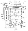
- a memory 100may include an array of memory cells MC arranged in rows WL and columns BL in accordance with one embodiment of the present invention. While a relatively small array is illustrated, the present invention is in no way limited to any particular size of an array. While the terms “rows,” “word lines,” “bit lines,” and “columns” are used herein, they are merely meant to be illustrative and are not limiting with respect to the type and style of the sensed array.
- the memory device 100includes a plurality of memory cells MC typically arranged in a matrix 105 .
- the memory cells MC in the matrix 105may be arranged in m rows and n columns with a word line WL 1 –WLm associated with each matrix row, and a bit line BL 1 –BLn associated with each matrix column.
- the memory device 100may also include a number of auxiliary lines including a supply voltage line Vdd, distributing a supply voltage Vdd through a chip including the memory device 100 , that, depending on the specific memory device embodiment, may be, typically, from 1 to 3 V, for example 1.8 V, and a ground voltage line GND distributing a ground voltage.
- a high voltage supply line Vamay provide a relatively high voltage, generated by devices (e.g. charge-pump voltage boosters not shown in the drawing) integrated on the same chip, or externally supplied to the memory device 100 .
- the high voltage Vamay be 4.5–5 V in one embodiment.
- the cell MCmay be any memory cell including a phase change memory cell.
- phase change memory cellsinclude those using chalcogenide memory element 18 a and an access, select, or threshold device 18 b coupled in series to the device 18 a .
- the threshold device 18 bmay be an ovonic threshold switch that can be made of a chalcogenide alloy that does not exhibit an amorphous to crystalline phase change and which undergoes a rapid, electric field initiated change in electrical conductivity that persists only so long as a holding voltage is present.
- a memory cell MC in the matrix 105is connected to a respective one of the word lines WL 1 –WLm and a respective one of the bit lines BL 1 –BLn.
- the storage element 18 amay have a first terminal connected to the respective bit line BL 1 –BLn and a second terminal connected to a first terminal of the associated device 18 b .
- the device 18 bmay have a second terminal connected to a word line WL 1 –WLm.
- the storage element 18 amay be connected to the respective word line WL 1 –WLm and the device 18 b , associated with the storage element 18 a , may be connected to the respective bit line BL 1 –BLn.
- a memory cell MC within the matrix 105is accessed by selecting the corresponding row and column pair, i.e. by selecting the corresponding word line and bit line pair.
- Word line selector circuits 110 and bit line selector circuits 115may perform the selection of the word lines and of the bit lines on the basis of a row address binary code RADD and a column address binary code CADD, respectively, part of a memory address binary code ADD, for example received by the memory device 100 from a device external to the memory (e.g., a microprocessor).
- the word line selector circuits 110may decode the row address code RADD and select a corresponding one of the word lines WL 1 –WLm, identified by the specific row address code RADD received.
- the bit line selector circuits 115may decode the column address code CADD and select a corresponding bit line or, more generally, a corresponding bit line packet of the bit lines BL 1 –BLn. For example, the number of selected bit lines depending on the number of data words that can be read during a burst reading operation on the memory device 100 .
- a bit line BL 1 –BLnmay be identified by the received specific column address code CADD.
- the bit line selector circuits 115interface with read/write circuits 120 .
- the read/write circuits 120enable the writing of desired logic values into the selected memory cells MC, and reading of the logic values currently stored therein.
- the read/write circuits 120include sense amplifiers together with comparators, reference current/voltage generators, and current pulse generators for reading the logic values stored in the memory cells MC.
- the word line selection circuits 110may keep the word lines WL 1 –WLm at a relatively high de-selection voltage Vdes (e.g., a voltage roughly equal to half the high voltage Va (Va/2)).
- Vdese.g., a voltage roughly equal to half the high voltage Va (Va/2)
- the bit line selection circuits 115may keep the bit lines BL 1 –BLn disconnected, and thus isolated, from the read/write circuits 120 or, alternatively, at the de-selection voltage Vdes. In this way, none of the memory cells MC is accessed, since the bit lines BL 1 –BLn are floating or a voltage approximately equal to zero is dropped across the access elements 18 b.
- the word line selection circuits 110may lower the voltage of a selected one of the word lines WL 1 –WLm to a word line selection voltage V WL (for example, having a value equal to 0V—the ground potential), while the remaining word lines may be kept at the word line de-selection voltage Vdes in one embodiment.
- the bit line selection circuits 115may couple a selected one of the bit lines BL 1 –BLn (more typically, a selected bit line packet) to the read/write circuits 120 , while the remaining, non-selected bit lines may be left floating or held at the de-selection voltage, Vdes.
- the read/write circuits 120force a suitable current pulse into each selected bit line BL 1 –BLn. The pulse amplitude depends on the reading or writing operations to be performed.
- a relatively high read current pulseis applied to each selected bit line in one embodiment.
- the read current pulsemay have a suitable amplitude and a suitable time duration.
- the read currentcauses the charging of stray capacitances C BL1 –C BLn (typically, of about 1 pF), intrinsically associated with the bit lines BL 1 –BLn, and, accordingly, a corresponding transient of a bit line voltage V BL at each selected bit line BL 1 –BLn.
- the respective bit line voltageraises towards a corresponding steady-state value, depending on the resistance of the storage element 18 a , i.e., on the logic value stored in the selected memory cell MC.
- the duration of the transientdepends on the state of the storage element 18 a . If the storage element 18 a is in the crystalline state and the threshold device 18 b is switched on, a cell current flowing through the selected memory cell MC has an amplitude greater than the amplitude in the case where the storage element 18 a is in the higher resistivity or reset state.
- the logic value stored in the memory cell MCmay, in one embodiment, be evaluated by means of a comparison of the bit line voltage (or another voltage related to the bit line voltage) at, or close to, the steady state thereof with a suitable reference voltage, for example, obtained exploiting a service reference memory cell.
- the reference voltagecan, for example, be chosen to be an intermediate value between the bit line voltage when a logic value “0” is stored and the bit line voltage when a logic value “1” is stored.
- bit line discharge circuits 125 1 - 125 nare provided, associated with the bit lines BL 1 –BLn.
- the bit line discharge circuits 125 1 – 125 nmay be enabled in a bit line discharge phase of the memory device operation, preceding any operation, for discharging the bit line stray capacitances C BL1 –C BLn , in one embodiment.
- the bit line discharge circuits 125 1 – 125 nmay be implemented by means of transistors, particularly N-channel MOSFETs having a drain terminal connected to the corresponding bit line BL 1 –BLn, a source terminal connected to a de-selection voltage supply line Vdes providing the de-selection voltage Vdes and a gate terminal controlled by a discharge enable signal DIS_EN in one embodiment.
- the discharge enable signal DIS_ENmay be temporarily asserted to a sufficiently high positive voltage, so that all the discharge MOSFETs turn on and connect the bit lines BL 1 –BLn to the de-selection voltage supply line Vdes.
- the discharge currents that flow through the discharge transistorscause the discharge of the bit line stray capacitances C BL1 –C BLn for reaching the de-selection voltage Vdes. Then, before selecting the desired word line WL 1 –WLm, the discharge enable signal DIS_EN is de-asserted and the discharge MOSFETs turned off.
- a phase change material, used in the devices 18 a and 18 bmay include a chalcogenide material.
- a chalcogenide materialmay be a material that includes at least one element from column VI of the periodic table or may be a material that includes one or more of the chalcogen elements, e.g., any of the elements of tellurium, sulfur, or selenium.
- Chalcogenide materialsmay be non-volatile memory materials that may be used to store information that is retained even after the electrical power is removed.
- the phase change materialmay be chalcogenide element composition from the class of tellurium-germanium-antimony (Te x Ge y Sb z ) material or a GeSbTe alloy, although the scope of the present invention is not limited to just these materials.
- the memory materialmay be programmed into one of at least two memory states by applying an electrical signal to the memory material.
- An electrical signalmay alter the phase of the memory material between a substantially crystalline state and a substantially amorphous state, wherein the electrical resistance of the memory material in the substantially amorphous state is greater than the resistance of the memory material in the substantially crystalline state.
- the memory materialmay be adapted to be altered to a particular one of a number of resistance values within a range of resistance values to provide digital or analog storage of information.
- Programming of the memory material to alter the state or phase of the materialmay be accomplished by applying voltage potentials to the selected lines BL, WL, thereby generating a voltage potential across the memory material.
- An electrical currentmay flow through a portion of the memory material in response to the applied voltage potentials, and may result in heating of the memory material.
- This controlled heating and subsequent controlled coolingmay alter the memory state or phase of the memory material. Altering the phase or state of the memory material may alter an electrical characteristic of the memory material. For example, resistance of the material may be altered by altering the phase of the memory material. Either all or a portion of the phase change memory material may be altered during the writing pulse (i.e. only a portion/region of sensing device 18 a adjacent to either a top or bottom electrode may be phase changed during the write operation). In one embodiment, primarily the portion of memory material that undergoes phase change is the region that is adjacent to the smaller lower electrode.
- the memory materialmay also be referred to as a programmable resistive material or simply a programmable resistance material.
- a voltage pulse with a potential difference of about 0.5 to 1.5 voltsmay be applied across a portion of the memory material by applying about 0 volts to a lower line (e.g., a column line BL) and about 0.5 to 1.5 volts to an upper line (e.g., a row line WL).
- a current flowing through the memory material in response to the applied voltage potentialsmay result in heating of the memory material. This heating and subsequent cooling may alter the memory state or phase of the material.
- the memory materialIn a “reset” state, the memory material may be in an amorphous or semi-amorphous state and in a “set” state, the memory material may be in a crystalline or semi-crystalline state.
- the resistance of the memory material in the amorphous or semi-amorphous statemay be greater than the resistance of the material in the crystalline or semi-crystalline state.
- the memory materialmay be heated to a relatively higher temperature and then subsequently cooled at a fast rate to amorphisize memory material and “reset” memory material. Heating the volume or memory material to a relatively lower crystallization temperature may crystallize memory material and “set” memory material.
- Various resistances of memory materialmay be achieved to store information by varying the amount of current flow and duration through the volume of memory material, or by tailoring the edge rate of the trailing edge of the programming current or voltage pulse (that may impact the cooling rate of the select memory element).
- the information stored in memory materialmay be read by measuring the resistance of the memory material.
- a read currentmay be provided to the memory material using opposed lines BL, WL and a resulting read voltage across the memory material may be compared against a reference voltage using, for example, the sense amplifier.
- the read voltagemay be proportional to the resistance exhibited by the selected memory storage device 18 a.
- the threshold device 18 bwhich may be an OTS (Ovonic Threshold Switch) or equivalent, is off and may exhibit very high resistance in some embodiments.
- the off resistancecan, for example, range from 50,000 ohms to greater than 10 gigaohms at a bias of half the threshold voltage.
- the device 18 bmay remain in its off state until exceeding a threshold voltage or until a threshold current switches the device 18 b to a highly conductive, low resistance on state.
- the threshold voltagemay be on the order of 3.1 volts and the holding voltage may be on the order of 2.9 volts.
- the device 18 b voltage dropremains close to the holding voltage as the current passing through the device is increased, even if up to a relatively high, current level. Above that current level the device remains on but displays a finite differential resistance with the voltage drop increasing with increasing current.
- the device 18 bmay remain on until the current through the device 18 b is reduced below a characteristic holding current value that is dependent on the area of the material and may be impacted by the top and bottom electrodes utilized to form the device 18 b.
- the threshold device 18 bdoes not change phase. It remains permanently amorphous and its current-voltage characteristics may remain the same throughout its operating life.
- the holding currentmay be on the order of 10 to 100 micro-amps (uA) in one embodiment. Below this holding current, the device 18 b turns off and returns to the high resistance regime at low voltage, low field.
- the threshold current for the device 18 bmay generally be of the same order as the holding current.
- the holding currentmay be altered by changing process variables, such as the top and bottom electrode material and the chalcogenide material.
- the device 18 bmay provide high “on current” for a given area of device compared to conventional access devices such as metal oxide semiconductor field effect transistors or bipolar junction transistors or semiconductor diodes. However, such devices may also be used in some embodiments.
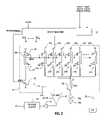
- the bit line selector circuits 115may include a current source 16 .
- the current source 16may controllably provide the current needed by the selected bit line for either reading, writing, or writing either a set or a reset bit. Each of these operations requires a different current.
- a single current source 16controllably supplies the appropriate current for each of these operations. Control over the current supplied may be provided by a control 32 .
- the control 32may be a processor and may include a state machine 12 .
- the state machine 12 of the control 32may communicate with the current source 16 .
- the state machine 12may receive reset current settings and read current settings as indicated in FIG. 2 .
- the reset current settingsprovide information about what current should be provided for writing a reset bit.
- the read current settingsprovide information about what current should be used for reading. The information may change from wafer run to run. That is, variations in wafers in particular runs may be accounted for by providing appropriate inputs to the state machine 12 .
- the state machine 12receives information about whether a read operation is implemented or whether a set or reset bit is to be written. Also, the state machine receives a clock signal.
- the state machine 12outputs a number of enable signals EN 1 –EN N .
- Nis equal to 32.
- different numbers of enable signals ENmay be utilized to provide different granularities in the amount of current provided by the current source 16 .
- the state machine 12may also either generate or pass through an external voltage signal VIREF that is applied to the gate of a transistor 26 . That signal may be generated, in some embodiments, based on the read current settings provided from external sources, for example, based on the characteristics of a particular wafer run.
- the amount of drive on the gate of the transistor 26may control the potential at the node PBIAS.
- the amount of current developed by the cascode 20 amay be controlled.
- the cascode 20 a and the transistor 26are part of a reference circuit which generates a reference current. That reference current from the reference circuit may then be mirrored into any of the cascodes 20 b – 20 n .
- the number of cascodes 20 b – 20 nmay be equal to the number of enable signals EN from the state machine 12 .
- the state machine 12can enable all or any subset of the cascodes 20 b – 20 n .
- each cascodemay have a transistor 24 (i.e., one of the transistors 24 a – 24 n ), which receives an enable signal EN as indicated.
- each enable signal from the state machineis designated for a particular cascode 20 b – 20 n in one embodiment of the present invention.
- the amount of current indicated by the arrows coming from each cascode 24 a – 24 nmay be determined in two ways. In the first way, the state machine 12 determines whether or not the cascode 24 is enabled. If a cascode is enabled, the amount of current that it passes is determined by the reference circuit and, particularly, by the drive on the gate of the transistor 26 .
- the current through the transistor 26 and its cascode 20 ais mirrored into each of the cascodes 20 b – 20 n .
- that currentis approximately 5 microamps.
- the node VC at the base of the cascodes 20 b – 20 nreceives whatever current is mirrored into each active cascode 20 .
- the node VCthen develops a voltage which is determined by the resistance across the selected cell MC, made up of the memory element 18 a and the threshold device 18 b .
- a pass transistor 28provides the current through the node VC and through the threshold device 18 b to ground.
- the node VCmay also be coupled through a switch 29 to an I/O pad so that the voltage VC may be monitored externally, for example, to determine what the reference voltage should be.
- the node VCmay also be coupled to an operational amplifier 50 , in one embodiment, that compares the voltage at the node VC to a reference voltage VREF from an external source, for example.
- the reference voltagemay be set between the voltage levels at the node VC for the set and reset bits.
- the operational amplifier 50is only turned on in the read mode by using the enable signal OP EN.
- the output from the operational amplifier 50is passed through an inverter 52 to a tristate buffer 54 .
- the operational amplifieracts as a sense amplifier to develop an output signal, indicated as I/O in FIG. 2 , indicating the state of a sensed cell.
- the reference voltagemay be set on the fly based on the characteristics of a particular run of wafers.
- the reference voltagemay be supplied from an external pad on a test chip.
- itmay be determined by the state machine 12 based on the various inputs received by the state machine 12 .
- the current in the reference circuitmay be adjusted as needed by setting the voltage VIREF. It is also possible to adjust the number of cascodes 20 that feed current to the node VC. These operations may be implemented under the control of the state machine 12 in some embodiments of the present invention. However, in some embodiments, it may be preferable to selectively operate the cascodes 20 b – 20 n because it may be undesirable to have the reference voltage vary for programming and read.
- a command to write a reset level to a selected cellmay have the characteristics over time as indicated in the upper plot.
- This internal signalmay have an adjustable delay between the time t 1 and t 2 in some embodiments. This adjustable delay may allow the pulse width of the resulting signal, indicated between the times t 2 and t 3 in FIG. 3 , to be controllably adjusted.
- a reset command signal of a larger pulse widtha smaller pulse width internal command signal may be generated.
- That internal command signalmay be a square wave in one embodiment.
- the current to write a reset bit into the selected cellmay be a square wave of determined pulse width.
- the determination of the pulse widthmay be dynamically controlled by the state machine 12 in one embodiment of the present invention by setting the time delay between the time that the state machine 12 receives the external write command, indicated as a set signal, and the time, t 2 , when the state machine 12 provides the enable signal to the appropriate cascodes 20 b – 20 n to generate current to the node V C .
- one or more additional pulsesmay be applied in some embodiments of the present invention.
- the initial pulsemay be at a relatively lower start amplitude as indicated in FIG. 3 .
- Some bitsmay need a higher amplitude programming pulse than other bits to reach the reset state.
- a checkdetermines whether or not any bits still need to be reset after the initial start pulse amplitude is applied. If so, a second pulse may be applied, for example, between times t 5 and t 6 , as indicated in FIG. 3 .
- the start pulse amplitudemay be incremented to provide a slightly higher first incremented amplitude, second pulse as indicated in FIG. 3 .
- progressively higher pulsesmay be applied until all the bits are reset or until a maximum amplitude is reached.
- the maximum amplitudemay be an amplitude that would lead to early wear out or difficulty in achieving a subsequent set state.
- the higher amplitude pulsesmay be achieved by simply activating additional current mirrors as needed in some embodiments.
- the write a set bit command from an external sourcesimilarly has a pulse width from time t 1 to t 3 .
- the internal response theretois generated by the state machine 12 .
- That signal EN 1 –ENnmay have a fixed delay between the time t 1 and t 2 in one embodiment. After the fixed delay, represented by the time t 1 –t 2 , a square pulse may be generated between the time t 2 and t 3 .
- the square pulseshown in FIGS. 3 and 4 , may be generated by operating a predetermined number of the cascodes 20 .
- 28 out of 32 available cascodesmay be operated between the times t 2 and t 3 .
- a rampis provided after time t 3 to time t 4 .
- the rampmay be provided by turning off the active cascodes 20 one after another in timed sequence, to achieve the desired ramp slope.
- the cascode 20 disable signalsmay be timed by the clock input to the state machine 12 in one embodiment of the present invention.
- the width of the programming pulse, and the slope of its rampmay be set based on inputs to the state machine 12 .
- Those inputsmay include a variety of data including the characteristics of the memory element 18 a and the particular characteristics of a run of wafers.
- the circuit shown in FIG. 2may be used in a variety of conditions for a variety of different memory arrays without substantial redesign of the current source 16 . This makes the current source 16 particularly adaptable to prototype development and test chips.
- a highly dynamic, programmable current source 16is provided that can programmably provide read and write currents as needed based on a variety of factors for a variety of different matrices 105 of memory cells.
- the memory cells in any given matrix 105may have differences from design to design and from wafer to wafer, which may be accommodated through the operation of the state machine 12 and the controllable current source 16 .
- the current source 16advantageously provides single, variable level current source for reading and writing both set and reset bits in some embodiments.
- programmingmay be achieved using currents in the range of 300 microamps to 4.8 milliamps.
- programming in the set modemay involve changing the material to a crystalline state by keeping the temperature of the material between its melting point and its glass transition temperature for 20 to 50 nanoseconds.
- Programming for the reset modemay involve changing the state of the material to an amorphous state by raising the temperature of the memory material to its melting point for a short duration, such as less than 2 nanoseconds in one embodiment.
- cell currentsranging from 3 microamps to 50 microamps may be applied in some embodiments.
- the delay between time t 1 and time t 2 for a reset signalmay, for example, be between 10 nanoseconds and 40 nanoseconds.
- the delay between time t 1 and t 2 for a set signalmay be between 0.3 and 1.7 microsecond.
- different numbers of the cascodesmay be operational in the read mode and in writing set and reset bits.
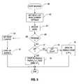
- the state machine code 60may initially get the reset, set, and read current settings as indicated in block 62 .
- the code 60may be software, firmware, or hardware. These settings may be provided from external sources or may be calculated based on available information.
- the operation to be performedis then received and the appropriate currents calculated as indicated in block 64 .
- a checkdetermines whether the state machine 12 is in the program mode. If so, a first check is whether or not a set bit will be written as indicated in diamond 72 . If so, the delay between the times t 1 and t 2 is determined (block 74 ) and the appropriate number of enable signals are generated between the times t 2 (block 76 ) and t 3 (block 76 ).
- the appropriate number of enable signalsare provided between the time t 2 through t 3 (block 78 ). Thereafter, the current is ramped down to time t 4 .
- the rampingmay be implemented, in one embodiment, by progressively turning off enable signals EN using the clock input to the state machine 12 to time the progressive turning off of the cascode enable signals.
- the read currentmay be set as indicated in block 68 . This may be done by controlling the signal VIREF to set the reference column current in one embodiment. In some embodiments, the read current may be set wafer to wafer at a level between the set and reset bits. However, other arrangements are also possible.
- the operational amplifier enable signal OP ENis enabled to turn on the operational amplifiers 50 . The enable signals are then driven, as indicated in block 70 , to provide the desired read current.
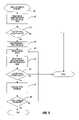
- a series of pulsesmay be applied to program the reset bit. This may be necessary because some bits may need a higher voltage to be programmed than other bits. However at the same time, it is desirable not to exceed a maximum safe pulse amplitude.
- the data to programis received as indicated at 80 .
- the datais read to determine which bits need to be reset as indicated in block 82 .
- a check at diamond 84determines whether any bits need a program pulse.
- those bitsreceive a program pulse at the start amplitude as indicated in block 86 and block 88 .
- the datais then read to determine which bits still need to be reset as indicated in block 90 .
- each bit in the arraymay have different optimal pulse amplitude for reset, different pulse amplitudes may be used. However, applying at pulse greater than the optimal pulse may damage the bit leading to early wear out, and difficulty in achieving a subsequent set state.
- System 500may be used in wireless devices such as, for example, a personal digital assistant (PDA), a laptop or portable computer with wireless capability, a web tablet, a wireless telephone, a pager, an instant messaging device, a digital music player, a digital camera, or other devices that may be adapted to transmit and/or receive information wirelessly.
- PDApersonal digital assistant
- System 500may be used in any of the following systems: a wireless local area network (WLAN) system, a wireless personal area network (WPAN) system, or a cellular network, although the scope of the present invention is not limited in this respect.
- WLANwireless local area network
- WPANwireless personal area network
- cellular networkalthough the scope of the present invention is not limited in this respect.
- System 500may include a controller 510 , an input/output (I/O) device 520 (e.g. a keypad, display), a memory 100 , a wireless interface 540 , and a static random access memory (SRAM) 560 and coupled to each other via a bus 550 .
- I/Oinput/output
- a battery 580may supply power to the system 500 in one embodiment. It should be noted that the scope of the present invention is not limited to embodiments having any or all of these components.
- Controller 510may comprise, for example, one or more microprocessors, digital signal processors, micro-controllers, or the like.
- Memory 100may be used to store messages transmitted to or by system 500 .
- Memory 100may also optionally be used to store instructions that are executed by controller 510 during the operation of system 500 , and may be used to store user data.
- the instructionsmay be stored as digital information and the user data, as disclosed herein, may be stored in one section of the memory as digital data and in another section as analog memory.
- a given section at one timemay be labeled as such and store digital information, and then later may be relabeled and reconfigured to store analog information.
- Memory 100may be provided by one or more different types of memory.
- memory 100may comprise a volatile memory (any type of random access memory), a non-volatile memory such as a flash memory, and/or memory 100 illustrated in FIG. 1 .
- the I/O device 520may be used to generate a message.
- the system 500may use the wireless interface 540 to transmit and receive messages to and from a wireless communication network with a radio frequency (RF) signal.
- RFradio frequency
- Examples of the wireless interface 540may include an antenna, or a wireless transceiver, such as a dipole antenna, although the scope of the present invention is not limited in this respect.
- the I/O device 520may deliver a voltage reflecting what is stored as either a digital output (if digital information was stored), or it may be analog information (if analog information was stored).
Landscapes
- Chemical & Material Sciences (AREA)
- Crystallography & Structural Chemistry (AREA)
- Semiconductor Memories (AREA)
Abstract
Description
Claims (6)
Priority Applications (4)
| Application Number | Priority Date | Filing Date | Title |
|---|---|---|---|
| US11/058,797US7099180B1 (en) | 2005-02-15 | 2005-02-15 | Phase change memory bits reset through a series of pulses of increasing amplitude |
| PCT/US2006/003317WO2006088635A1 (en) | 2005-02-15 | 2006-01-30 | Resetting phase change memory bits |
| US11/486,872US7313016B2 (en) | 2005-02-15 | 2006-07-14 | Method of resetting phase change memory bits through a series of pulses of increasing amplitude |
| US11/983,479US7518904B2 (en) | 2005-02-15 | 2007-11-09 | Method of resetting phase change memory bits through a series of pulses of increasing amplitude |
Applications Claiming Priority (1)
| Application Number | Priority Date | Filing Date | Title |
|---|---|---|---|
| US11/058,797US7099180B1 (en) | 2005-02-15 | 2005-02-15 | Phase change memory bits reset through a series of pulses of increasing amplitude |
Related Child Applications (1)
| Application Number | Title | Priority Date | Filing Date |
|---|---|---|---|
| US11/486,872DivisionUS7313016B2 (en) | 2005-02-15 | 2006-07-14 | Method of resetting phase change memory bits through a series of pulses of increasing amplitude |
Publications (2)
| Publication Number | Publication Date |
|---|---|
| US20060181922A1 US20060181922A1 (en) | 2006-08-17 |
| US7099180B1true US7099180B1 (en) | 2006-08-29 |
Family
ID=36444780
Family Applications (3)
| Application Number | Title | Priority Date | Filing Date |
|---|---|---|---|
| US11/058,797Expired - LifetimeUS7099180B1 (en) | 2005-02-15 | 2005-02-15 | Phase change memory bits reset through a series of pulses of increasing amplitude |
| US11/486,872Expired - LifetimeUS7313016B2 (en) | 2005-02-15 | 2006-07-14 | Method of resetting phase change memory bits through a series of pulses of increasing amplitude |
| US11/983,479Expired - Fee RelatedUS7518904B2 (en) | 2005-02-15 | 2007-11-09 | Method of resetting phase change memory bits through a series of pulses of increasing amplitude |
Family Applications After (2)
| Application Number | Title | Priority Date | Filing Date |
|---|---|---|---|
| US11/486,872Expired - LifetimeUS7313016B2 (en) | 2005-02-15 | 2006-07-14 | Method of resetting phase change memory bits through a series of pulses of increasing amplitude |
| US11/983,479Expired - Fee RelatedUS7518904B2 (en) | 2005-02-15 | 2007-11-09 | Method of resetting phase change memory bits through a series of pulses of increasing amplitude |
Country Status (2)
| Country | Link |
|---|---|
| US (3) | US7099180B1 (en) |
| WO (1) | WO2006088635A1 (en) |
Cited By (80)
| Publication number | Priority date | Publication date | Assignee | Title |
|---|---|---|---|---|
| US20060013058A1 (en)* | 2004-07-19 | 2006-01-19 | Samsung Electronics Co., Ltd. | Phase change memory device for use in a burst read operation and a data reading method thereof |
| US20060291272A1 (en)* | 2005-06-22 | 2006-12-28 | Lowrey Tyler A | Static random access memory cell using chalcogenide |
| US20070058425A1 (en)* | 2005-09-08 | 2007-03-15 | Woo-Yeong Cho | Phase change random access memory device having variable drive voltage circuit |
| US20070171705A1 (en)* | 2005-12-15 | 2007-07-26 | Parkinson Ward D | Writing phase change memories |
| US20080062754A1 (en)* | 2005-02-15 | 2008-03-13 | Dodge Rick K | Method of resetting phase change memory bits through a series of pulses of increasing amplitude |
| US20080123396A1 (en)* | 2004-04-02 | 2008-05-29 | Semiconductor Energy Laboratory Co., Ltd. | Semiconductor Device and Driving Method of the Same |
| US20080180990A1 (en)* | 2007-01-31 | 2008-07-31 | Macronix International Co., Ltd. | Method to tighten set distribution for pcram |
| US20080316792A1 (en)* | 2007-06-21 | 2008-12-25 | Jan Boris Philipp | Circuit for programming a memory element |
| US20090086534A1 (en)* | 2007-10-01 | 2009-04-02 | Debrosse John K | Apparatus and method for implementing precise sensing of pcram devices |
| US7560337B2 (en) | 2006-01-09 | 2009-07-14 | Macronix International Co., Ltd. | Programmable resistive RAM and manufacturing method |
| US7569844B2 (en) | 2007-04-17 | 2009-08-04 | Macronix International Co., Ltd. | Memory cell sidewall contacting side electrode |
| US20090219749A1 (en)* | 2008-02-29 | 2009-09-03 | Lamorey Mark C H | Method and apparatus for implementing concurrent multiple level sensing operation for resistive memory devices |
| US7593255B2 (en) | 2007-12-07 | 2009-09-22 | Qimonda North America Corp. | Integrated circuit for programming a memory element |
| US20090244962A1 (en)* | 2008-03-31 | 2009-10-01 | George Gordon | Immunity of phase change material to disturb in the amorphous phase |
| US7599217B2 (en) | 2005-11-22 | 2009-10-06 | Macronix International Co., Ltd. | Memory cell device and manufacturing method |
| US7688619B2 (en) | 2005-11-28 | 2010-03-30 | Macronix International Co., Ltd. | Phase change memory cell and manufacturing method |
| US7701750B2 (en) | 2008-05-08 | 2010-04-20 | Macronix International Co., Ltd. | Phase change device having two or more substantial amorphous regions in high resistance state |
| US20100097850A1 (en)* | 2004-07-09 | 2010-04-22 | Samsung Electronics Co., Ltd. | Apparatus and systems using phase change memories |
| US20100103717A1 (en)* | 2008-10-27 | 2010-04-29 | Seagate Technology Llc | Tuning a variable resistance of a resistive sense element |
| US7719913B2 (en) | 2008-09-12 | 2010-05-18 | Macronix International Co., Ltd. | Sensing circuit for PCRAM applications |
| US7741636B2 (en) | 2006-01-09 | 2010-06-22 | Macronix International Co., Ltd. | Programmable resistive RAM and manufacturing method |
| US7749854B2 (en) | 2006-12-06 | 2010-07-06 | Macronix International Co., Ltd. | Method for making a self-converged memory material element for memory cell |
| US7785920B2 (en) | 2006-07-12 | 2010-08-31 | Macronix International Co., Ltd. | Method for making a pillar-type phase change memory element |
| US7786460B2 (en) | 2005-11-15 | 2010-08-31 | Macronix International Co., Ltd. | Phase change memory device and manufacturing method |
| US7786461B2 (en) | 2007-04-03 | 2010-08-31 | Macronix International Co., Ltd. | Memory structure with reduced-size memory element between memory material portions |
| US7791057B2 (en) | 2008-04-22 | 2010-09-07 | Macronix International Co., Ltd. | Memory cell having a buried phase change region and method for fabricating the same |
| US7863655B2 (en) | 2006-10-24 | 2011-01-04 | Macronix International Co., Ltd. | Phase change memory cells with dual access devices |
| US7869270B2 (en) | 2008-12-29 | 2011-01-11 | Macronix International Co., Ltd. | Set algorithm for phase change memory cell |
| US7894254B2 (en) | 2009-07-15 | 2011-02-22 | Macronix International Co., Ltd. | Refresh circuitry for phase change memory |
| US7902538B2 (en) | 2005-11-28 | 2011-03-08 | Macronix International Co., Ltd. | Phase change memory cell with first and second transition temperature portions |
| US7903447B2 (en) | 2006-12-13 | 2011-03-08 | Macronix International Co., Ltd. | Method, apparatus and computer program product for read before programming process on programmable resistive memory cell |
| US7903457B2 (en) | 2008-08-19 | 2011-03-08 | Macronix International Co., Ltd. | Multiple phase change materials in an integrated circuit for system on a chip application |
| US7910906B2 (en) | 2006-10-04 | 2011-03-22 | Macronix International Co., Ltd. | Memory cell device with circumferentially-extending memory element |
| US20110069538A1 (en)* | 2009-09-22 | 2011-03-24 | International Business Machines Corporation | Multi-level cell programming of pcm by varying the reset amplitude |
| US7919766B2 (en) | 2007-10-22 | 2011-04-05 | Macronix International Co., Ltd. | Method for making self aligning pillar memory cell device |
| US7932506B2 (en) | 2008-07-22 | 2011-04-26 | Macronix International Co., Ltd. | Fully self-aligned pore-type memory cell having diode access device |
| US7933139B2 (en) | 2009-05-15 | 2011-04-26 | Macronix International Co., Ltd. | One-transistor, one-resistor, one-capacitor phase change memory |
| US7956344B2 (en) | 2007-02-27 | 2011-06-07 | Macronix International Co., Ltd. | Memory cell with memory element contacting ring-shaped upper end of bottom electrode |
| US7968876B2 (en) | 2009-05-22 | 2011-06-28 | Macronix International Co., Ltd. | Phase change memory cell having vertical channel access transistor |
| US7978509B2 (en) | 2007-08-02 | 2011-07-12 | Macronix International Co., Ltd. | Phase change memory with dual word lines and source lines and method of operating same |
| US7993962B2 (en) | 2005-11-15 | 2011-08-09 | Macronix International Co., Ltd. | I-shaped phase change memory cell |
| US8030635B2 (en) | 2009-01-13 | 2011-10-04 | Macronix International Co., Ltd. | Polysilicon plug bipolar transistor for phase change memory |
| US8036014B2 (en) | 2008-11-06 | 2011-10-11 | Macronix International Co., Ltd. | Phase change memory program method without over-reset |
| US8064247B2 (en) | 2009-01-14 | 2011-11-22 | Macronix International Co., Ltd. | Rewritable memory device based on segregation/re-absorption |
| US8064248B2 (en) | 2009-09-17 | 2011-11-22 | Macronix International Co., Ltd. | 2T2R-1T1R mix mode phase change memory array |
| US8062833B2 (en) | 2005-12-30 | 2011-11-22 | Macronix International Co., Ltd. | Chalcogenide layer etching method |
| US8077505B2 (en) | 2008-05-07 | 2011-12-13 | Macronix International Co., Ltd. | Bipolar switching of phase change device |
| US8084760B2 (en) | 2009-04-20 | 2011-12-27 | Macronix International Co., Ltd. | Ring-shaped electrode and manufacturing method for same |
| US8089137B2 (en) | 2009-01-07 | 2012-01-03 | Macronix International Co., Ltd. | Integrated circuit memory with single crystal silicon on silicide driver and manufacturing method |
| US8097871B2 (en) | 2009-04-30 | 2012-01-17 | Macronix International Co., Ltd. | Low operational current phase change memory structures |
| US8107283B2 (en) | 2009-01-12 | 2012-01-31 | Macronix International Co., Ltd. | Method for setting PCRAM devices |
| US8110822B2 (en) | 2009-07-15 | 2012-02-07 | Macronix International Co., Ltd. | Thermal protect PCRAM structure and methods for making |
| US8110430B2 (en) | 2005-11-21 | 2012-02-07 | Macronix International Co., Ltd. | Vacuum jacket for phase change memory element |
| US8134857B2 (en) | 2008-06-27 | 2012-03-13 | Macronix International Co., Ltd. | Methods for high speed reading operation of phase change memory and device employing same |
| US8173987B2 (en) | 2009-04-27 | 2012-05-08 | Macronix International Co., Ltd. | Integrated circuit 3D phase change memory array and manufacturing method |
| US8178387B2 (en) | 2009-10-23 | 2012-05-15 | Macronix International Co., Ltd. | Methods for reducing recrystallization time for a phase change material |
| US8178405B2 (en) | 2006-12-28 | 2012-05-15 | Macronix International Co., Ltd. | Resistor random access memory cell device |
| US8198619B2 (en) | 2009-07-15 | 2012-06-12 | Macronix International Co., Ltd. | Phase change memory cell structure |
| US8203899B2 (en)* | 2008-10-31 | 2012-06-19 | Seagate Technology Llc | Memory cell with proportional current self-reference sensing |
| US8238149B2 (en) | 2009-06-25 | 2012-08-07 | Macronix International Co., Ltd. | Methods and apparatus for reducing defect bits in phase change memory |
| US20120262984A1 (en)* | 2008-03-31 | 2012-10-18 | Savransky Semyon D | Reducing Temporal Changes in Phase Change Memories |
| US8310864B2 (en) | 2010-06-15 | 2012-11-13 | Macronix International Co., Ltd. | Self-aligned bit line under word line memory array |
| US8324605B2 (en) | 2008-10-02 | 2012-12-04 | Macronix International Co., Ltd. | Dielectric mesh isolated phase change structure for phase change memory |
| US8350316B2 (en) | 2009-05-22 | 2013-01-08 | Macronix International Co., Ltd. | Phase change memory cells having vertical channel access transistor and memory plane |
| US8363463B2 (en) | 2009-06-25 | 2013-01-29 | Macronix International Co., Ltd. | Phase change memory having one or more non-constant doping profiles |
| US8395935B2 (en) | 2010-10-06 | 2013-03-12 | Macronix International Co., Ltd. | Cross-point self-aligned reduced cell size phase change memory |
| US8406033B2 (en) | 2009-06-22 | 2013-03-26 | Macronix International Co., Ltd. | Memory device and method for sensing and fixing margin cells |
| US8415651B2 (en) | 2008-06-12 | 2013-04-09 | Macronix International Co., Ltd. | Phase change memory cell having top and bottom sidewall contacts |
| US8462537B2 (en) | 2011-03-21 | 2013-06-11 | Intel Corporation | Method and apparatus to reset a phase change memory and switch (PCMS) memory cell |
| US8467238B2 (en) | 2010-11-15 | 2013-06-18 | Macronix International Co., Ltd. | Dynamic pulse operation for phase change memory |
| US8497705B2 (en) | 2010-11-09 | 2013-07-30 | Macronix International Co., Ltd. | Phase change device for interconnection of programmable logic device |
| US20130294147A1 (en)* | 2008-10-09 | 2013-11-07 | Kabushiki Kaisha Toshiba | Resistance change memory |
| US8729521B2 (en) | 2010-05-12 | 2014-05-20 | Macronix International Co., Ltd. | Self aligned fin-type programmable memory cell |
| US8809829B2 (en) | 2009-06-15 | 2014-08-19 | Macronix International Co., Ltd. | Phase change memory having stabilized microstructure and manufacturing method |
| US20140376308A1 (en)* | 2013-06-21 | 2014-12-25 | Macronix International Co., Ltd. | Phase change memory, writing method thereof and reading method thereof |
| US8933536B2 (en) | 2009-01-22 | 2015-01-13 | Macronix International Co., Ltd. | Polysilicon pillar bipolar transistor with self-aligned memory element |
| US9559113B2 (en) | 2014-05-01 | 2017-01-31 | Macronix International Co., Ltd. | SSL/GSL gate oxide in 3D vertical channel NAND |
| US9672906B2 (en) | 2015-06-19 | 2017-06-06 | Macronix International Co., Ltd. | Phase change memory with inter-granular switching |
| US9934850B2 (en) | 2013-09-10 | 2018-04-03 | Micron Technology, Inc. | Accessing memory cells in parallel in a cross-point array |
| US10832770B2 (en) | 2019-03-13 | 2020-11-10 | Sandisk Technologies Llc | Single pulse memory operation |
Families Citing this family (20)
| Publication number | Priority date | Publication date | Assignee | Title |
|---|---|---|---|---|
| EP1895541A1 (en)* | 2006-09-01 | 2008-03-05 | STMicroelectronics S.r.l. | Method for reading phase change memories and phase change memory |
| US20080101110A1 (en)* | 2006-10-25 | 2008-05-01 | Thomas Happ | Combined read/write circuit for memory |
| KR100781550B1 (en) | 2006-11-08 | 2007-12-03 | 삼성전자주식회사 | Phase change memory device and its firing method |
| US8194433B2 (en)* | 2008-02-20 | 2012-06-05 | Ovonyx, Inc. | Method and apparatus for accessing a bidirectional memory |
| TWI517156B (en)* | 2008-02-29 | 2016-01-11 | Toshiba Kk | Semiconductor memory device |
| KR100998944B1 (en)* | 2008-12-26 | 2010-12-09 | 주식회사 하이닉스반도체 | Pram's Light Driver Circuit |
| US8377741B2 (en)* | 2008-12-30 | 2013-02-19 | Stmicroelectronics S.R.L. | Self-heating phase change memory cell architecture |
| US8023345B2 (en)* | 2009-02-24 | 2011-09-20 | International Business Machines Corporation | Iteratively writing contents to memory locations using a statistical model |
| US8166368B2 (en)* | 2009-02-24 | 2012-04-24 | International Business Machines Corporation | Writing a special symbol to a memory to indicate the absence of a data signal |
| US8386739B2 (en)* | 2009-09-28 | 2013-02-26 | International Business Machines Corporation | Writing to memory using shared address buses |
| US8230276B2 (en)* | 2009-09-28 | 2012-07-24 | International Business Machines Corporation | Writing to memory using adaptive write techniques |
| WO2011074021A1 (en) | 2009-12-18 | 2011-06-23 | Mattia Boniardi | Modified reset state for enhanced read margin of phase change memory |
| US8463985B2 (en) | 2010-03-31 | 2013-06-11 | International Business Machines Corporation | Constrained coding to reduce floating gate coupling in non-volatile memories |
| KR101201840B1 (en)* | 2010-04-26 | 2012-11-15 | 에스케이하이닉스 주식회사 | Semiconductor memory apparatus |
| US8345472B2 (en)* | 2010-12-21 | 2013-01-01 | Intel Corporation | Three-terminal ovonic threshold switch as a current driver in a phase change memory |
| KR101544632B1 (en) | 2011-01-28 | 2015-08-18 | 한양대학교 산학협력단 | Memory of using Resistive Switching Device and Method of operating the same |
| US9711213B2 (en) | 2014-09-04 | 2017-07-18 | Micron Technology, Inc. | Operational signals generated from capacitive stored charge |
| US9583187B2 (en) | 2015-03-28 | 2017-02-28 | Intel Corporation | Multistage set procedure for phase change memory |
| US10497441B2 (en) | 2015-07-14 | 2019-12-03 | Hewlett Packard Enterprise Development Lp | Determining first write strength |
| CN110473583A (en)* | 2019-08-15 | 2019-11-19 | 山东华芯半导体有限公司 | A kind of operation detection method of NAND Flash |
Citations (9)
| Publication number | Priority date | Publication date | Assignee | Title |
|---|---|---|---|---|
| US4225946A (en) | 1979-01-24 | 1980-09-30 | Harris Corporation | Multilevel erase pulse for amorphous memory devices |
| US5537358A (en)* | 1994-12-06 | 1996-07-16 | National Semiconductor Corporation | Flash memory having adaptive sensing and method |
| US6327183B1 (en)* | 2000-01-10 | 2001-12-04 | Advanced Micro Devices, Inc. | Nonlinear stepped programming voltage |
| US6525961B2 (en)* | 2000-09-18 | 2003-02-25 | Stmicroelectronics, S.R.L. | Method and circuit for programming a multilevel non-volatile memory |
| US6714448B2 (en)* | 2002-07-02 | 2004-03-30 | Atmel Corporation | Method of programming a multi-level memory device |
| US20040114419A1 (en) | 2002-12-13 | 2004-06-17 | Lowrey Tyler A. | Method and system to store information |
| US6754107B2 (en)* | 2001-12-27 | 2004-06-22 | Stmicroelectronics S.R.L. | Single supply voltage, nonvolatile phase change memory device with cascoded column selection and simultaneous word read/write operations |
| EP1450373A1 (en) | 2003-02-21 | 2004-08-25 | STMicroelectronics S.r.l. | Phase change memory device |
| US20050141261A1 (en) | 2003-12-30 | 2005-06-30 | Su-Jin Ahn | Set programming methods and write driver circuits for a phase-change memory array |
Family Cites Families (1)
| Publication number | Priority date | Publication date | Assignee | Title |
|---|---|---|---|---|
| US7099180B1 (en)* | 2005-02-15 | 2006-08-29 | Intel Corporation | Phase change memory bits reset through a series of pulses of increasing amplitude |
- 2005
- 2005-02-15USUS11/058,797patent/US7099180B1/ennot_activeExpired - Lifetime
- 2006
- 2006-01-30WOPCT/US2006/003317patent/WO2006088635A1/enactiveApplication Filing
- 2006-07-14USUS11/486,872patent/US7313016B2/ennot_activeExpired - Lifetime
- 2007
- 2007-11-09USUS11/983,479patent/US7518904B2/ennot_activeExpired - Fee Related
Patent Citations (11)
| Publication number | Priority date | Publication date | Assignee | Title |
|---|---|---|---|---|
| US4225946A (en) | 1979-01-24 | 1980-09-30 | Harris Corporation | Multilevel erase pulse for amorphous memory devices |
| US5537358A (en)* | 1994-12-06 | 1996-07-16 | National Semiconductor Corporation | Flash memory having adaptive sensing and method |
| US6327183B1 (en)* | 2000-01-10 | 2001-12-04 | Advanced Micro Devices, Inc. | Nonlinear stepped programming voltage |
| US6525961B2 (en)* | 2000-09-18 | 2003-02-25 | Stmicroelectronics, S.R.L. | Method and circuit for programming a multilevel non-volatile memory |
| US6754107B2 (en)* | 2001-12-27 | 2004-06-22 | Stmicroelectronics S.R.L. | Single supply voltage, nonvolatile phase change memory device with cascoded column selection and simultaneous word read/write operations |
| US20040228163A1 (en)* | 2001-12-27 | 2004-11-18 | Stmicroelectronics S.R.L. | Phase change memory device |
| US6714448B2 (en)* | 2002-07-02 | 2004-03-30 | Atmel Corporation | Method of programming a multi-level memory device |
| US20040114419A1 (en) | 2002-12-13 | 2004-06-17 | Lowrey Tyler A. | Method and system to store information |
| US6813177B2 (en)* | 2002-12-13 | 2004-11-02 | Ovoynx, Inc. | Method and system to store information |
| EP1450373A1 (en) | 2003-02-21 | 2004-08-25 | STMicroelectronics S.r.l. | Phase change memory device |
| US20050141261A1 (en) | 2003-12-30 | 2005-06-30 | Su-Jin Ahn | Set programming methods and write driver circuits for a phase-change memory array |
Cited By (119)
| Publication number | Priority date | Publication date | Assignee | Title |
|---|---|---|---|---|
| US8045369B2 (en) | 2004-04-02 | 2011-10-25 | Semiconductor Energy Laboratory Co., Ltd. | Semiconductor device and driving method of the same |
| US7630233B2 (en)* | 2004-04-02 | 2009-12-08 | Semiconductor Energy Laboratory Co., Ltd. | Semiconductor device and driving method of the same |
| US20080123396A1 (en)* | 2004-04-02 | 2008-05-29 | Semiconductor Energy Laboratory Co., Ltd. | Semiconductor Device and Driving Method of the Same |
| US20100097850A1 (en)* | 2004-07-09 | 2010-04-22 | Samsung Electronics Co., Ltd. | Apparatus and systems using phase change memories |
| US8194442B2 (en) | 2004-07-09 | 2012-06-05 | Samsung Electronics Co., Ltd. | Apparatus and systems using phase change memories |
| US7944741B2 (en)* | 2004-07-09 | 2011-05-17 | Samsung Electronics Co., Ltd. | Apparatus and systems using phase change memories |
| US7280391B2 (en)* | 2004-07-19 | 2007-10-09 | Samsung Electronics Co., Llc | Phase change memory device for use in a burst read operation and a data reading method thereof |
| US20060013058A1 (en)* | 2004-07-19 | 2006-01-19 | Samsung Electronics Co., Ltd. | Phase change memory device for use in a burst read operation and a data reading method thereof |
| US20080062754A1 (en)* | 2005-02-15 | 2008-03-13 | Dodge Rick K | Method of resetting phase change memory bits through a series of pulses of increasing amplitude |
| US7518904B2 (en)* | 2005-02-15 | 2009-04-14 | Intel Corporation | Method of resetting phase change memory bits through a series of pulses of increasing amplitude |
| US20060291272A1 (en)* | 2005-06-22 | 2006-12-28 | Lowrey Tyler A | Static random access memory cell using chalcogenide |
| US7426135B2 (en)* | 2005-06-22 | 2008-09-16 | Ovonyx, Inc. | Static random access memory cell using chalcogenide |
| US20070058425A1 (en)* | 2005-09-08 | 2007-03-15 | Woo-Yeong Cho | Phase change random access memory device having variable drive voltage circuit |
| US7283387B2 (en)* | 2005-09-08 | 2007-10-16 | Samsung Electronics Co., Ltd. | Phase change random access memory device having variable drive voltage circuit |
| US8008114B2 (en) | 2005-11-15 | 2011-08-30 | Macronix International Co., Ltd. | Phase change memory device and manufacturing method |
| US7786460B2 (en) | 2005-11-15 | 2010-08-31 | Macronix International Co., Ltd. | Phase change memory device and manufacturing method |
| US7993962B2 (en) | 2005-11-15 | 2011-08-09 | Macronix International Co., Ltd. | I-shaped phase change memory cell |
| US8110430B2 (en) | 2005-11-21 | 2012-02-07 | Macronix International Co., Ltd. | Vacuum jacket for phase change memory element |
| US7599217B2 (en) | 2005-11-22 | 2009-10-06 | Macronix International Co., Ltd. | Memory cell device and manufacturing method |
| US7929340B2 (en) | 2005-11-28 | 2011-04-19 | Macronix International Co., Ltd. | Phase change memory cell and manufacturing method |
| US7902538B2 (en) | 2005-11-28 | 2011-03-08 | Macronix International Co., Ltd. | Phase change memory cell with first and second transition temperature portions |
| US7688619B2 (en) | 2005-11-28 | 2010-03-30 | Macronix International Co., Ltd. | Phase change memory cell and manufacturing method |
| US20070171705A1 (en)* | 2005-12-15 | 2007-07-26 | Parkinson Ward D | Writing phase change memories |
| US8062833B2 (en) | 2005-12-30 | 2011-11-22 | Macronix International Co., Ltd. | Chalcogenide layer etching method |
| US8178388B2 (en) | 2006-01-09 | 2012-05-15 | Macronix International Co., Ltd. | Programmable resistive RAM and manufacturing method |
| US7560337B2 (en) | 2006-01-09 | 2009-07-14 | Macronix International Co., Ltd. | Programmable resistive RAM and manufacturing method |
| US8158963B2 (en) | 2006-01-09 | 2012-04-17 | Macronix International Co., Ltd. | Programmable resistive RAM and manufacturing method |
| US7741636B2 (en) | 2006-01-09 | 2010-06-22 | Macronix International Co., Ltd. | Programmable resistive RAM and manufacturing method |
| US7785920B2 (en) | 2006-07-12 | 2010-08-31 | Macronix International Co., Ltd. | Method for making a pillar-type phase change memory element |
| US7910906B2 (en) | 2006-10-04 | 2011-03-22 | Macronix International Co., Ltd. | Memory cell device with circumferentially-extending memory element |
| US7863655B2 (en) | 2006-10-24 | 2011-01-04 | Macronix International Co., Ltd. | Phase change memory cells with dual access devices |
| US8110456B2 (en) | 2006-10-24 | 2012-02-07 | Macronix International Co., Ltd. | Method for making a self aligning memory device |
| US7749854B2 (en) | 2006-12-06 | 2010-07-06 | Macronix International Co., Ltd. | Method for making a self-converged memory material element for memory cell |
| US7903447B2 (en) | 2006-12-13 | 2011-03-08 | Macronix International Co., Ltd. | Method, apparatus and computer program product for read before programming process on programmable resistive memory cell |
| US8178405B2 (en) | 2006-12-28 | 2012-05-15 | Macronix International Co., Ltd. | Resistor random access memory cell device |
| US20080180990A1 (en)* | 2007-01-31 | 2008-07-31 | Macronix International Co., Ltd. | Method to tighten set distribution for pcram |
| US7535756B2 (en)* | 2007-01-31 | 2009-05-19 | Macronix International Co., Ltd. | Method to tighten set distribution for PCRAM |
| US7956344B2 (en) | 2007-02-27 | 2011-06-07 | Macronix International Co., Ltd. | Memory cell with memory element contacting ring-shaped upper end of bottom electrode |
| US7875493B2 (en) | 2007-04-03 | 2011-01-25 | Macronix International Co., Ltd. | Memory structure with reduced-size memory element between memory material portions |
| US7786461B2 (en) | 2007-04-03 | 2010-08-31 | Macronix International Co., Ltd. | Memory structure with reduced-size memory element between memory material portions |
| US7569844B2 (en) | 2007-04-17 | 2009-08-04 | Macronix International Co., Ltd. | Memory cell sidewall contacting side electrode |
| US20080316792A1 (en)* | 2007-06-21 | 2008-12-25 | Jan Boris Philipp | Circuit for programming a memory element |
| US7571901B2 (en) | 2007-06-21 | 2009-08-11 | Qimonda North America Corp. | Circuit for programming a memory element |
| US7978509B2 (en) | 2007-08-02 | 2011-07-12 | Macronix International Co., Ltd. | Phase change memory with dual word lines and source lines and method of operating same |
| US7535783B2 (en) | 2007-10-01 | 2009-05-19 | International Business Machines Corporation | Apparatus and method for implementing precise sensing of PCRAM devices |
| US20090086534A1 (en)* | 2007-10-01 | 2009-04-02 | Debrosse John K | Apparatus and method for implementing precise sensing of pcram devices |
| US7919766B2 (en) | 2007-10-22 | 2011-04-05 | Macronix International Co., Ltd. | Method for making self aligning pillar memory cell device |
| US8222071B2 (en) | 2007-10-22 | 2012-07-17 | Macronix International Co., Ltd. | Method for making self aligning pillar memory cell device |
| US7593255B2 (en) | 2007-12-07 | 2009-09-22 | Qimonda North America Corp. | Integrated circuit for programming a memory element |
| US20090219749A1 (en)* | 2008-02-29 | 2009-09-03 | Lamorey Mark C H | Method and apparatus for implementing concurrent multiple level sensing operation for resistive memory devices |
| US7778065B2 (en) | 2008-02-29 | 2010-08-17 | International Business Machines Corporation | Method and apparatus for implementing concurrent multiple level sensing operation for resistive memory devices |
| US8462546B2 (en)* | 2008-03-31 | 2013-06-11 | Intel Corporation | Reducing temporal changes in phase change memories |
| US20090244962A1 (en)* | 2008-03-31 | 2009-10-01 | George Gordon | Immunity of phase change material to disturb in the amorphous phase |
| US7990761B2 (en) | 2008-03-31 | 2011-08-02 | Ovonyx, Inc. | Immunity of phase change material to disturb in the amorphous phase |
| US9251895B2 (en) | 2008-03-31 | 2016-02-02 | Carlow Innovations Llc | Immunity of phase change material to disturb in the amorphous phase |
| US9036409B2 (en) | 2008-03-31 | 2015-05-19 | Ovonyx, Inc. | Immunity of phase change material to disturb in the amorphous phase |
| US20120262984A1 (en)* | 2008-03-31 | 2012-10-18 | Savransky Semyon D | Reducing Temporal Changes in Phase Change Memories |
| US7791057B2 (en) | 2008-04-22 | 2010-09-07 | Macronix International Co., Ltd. | Memory cell having a buried phase change region and method for fabricating the same |
| US8077505B2 (en) | 2008-05-07 | 2011-12-13 | Macronix International Co., Ltd. | Bipolar switching of phase change device |
| US8059449B2 (en) | 2008-05-08 | 2011-11-15 | Macronix International Co., Ltd. | Phase change device having two or more substantial amorphous regions in high resistance state |
| US7701750B2 (en) | 2008-05-08 | 2010-04-20 | Macronix International Co., Ltd. | Phase change device having two or more substantial amorphous regions in high resistance state |
| US8415651B2 (en) | 2008-06-12 | 2013-04-09 | Macronix International Co., Ltd. | Phase change memory cell having top and bottom sidewall contacts |
| US8134857B2 (en) | 2008-06-27 | 2012-03-13 | Macronix International Co., Ltd. | Methods for high speed reading operation of phase change memory and device employing same |
| US7932506B2 (en) | 2008-07-22 | 2011-04-26 | Macronix International Co., Ltd. | Fully self-aligned pore-type memory cell having diode access device |
| US7903457B2 (en) | 2008-08-19 | 2011-03-08 | Macronix International Co., Ltd. | Multiple phase change materials in an integrated circuit for system on a chip application |
| US8315088B2 (en) | 2008-08-19 | 2012-11-20 | Macronix International Co., Ltd. | Multiple phase change materials in an integrated circuit for system on a chip application |
| US7719913B2 (en) | 2008-09-12 | 2010-05-18 | Macronix International Co., Ltd. | Sensing circuit for PCRAM applications |
| US8324605B2 (en) | 2008-10-02 | 2012-12-04 | Macronix International Co., Ltd. | Dielectric mesh isolated phase change structure for phase change memory |
| US8681532B2 (en)* | 2008-10-09 | 2014-03-25 | Kabushiki Kaisha Toshiba | Resistance change memory |
| US20130294147A1 (en)* | 2008-10-09 | 2013-11-07 | Kabushiki Kaisha Toshiba | Resistance change memory |
| US8289748B2 (en)* | 2008-10-27 | 2012-10-16 | Seagate Technology Llc | Tuning a variable resistance of a resistive sense element |
| US20100103717A1 (en)* | 2008-10-27 | 2010-04-29 | Seagate Technology Llc | Tuning a variable resistance of a resistive sense element |
| US8203899B2 (en)* | 2008-10-31 | 2012-06-19 | Seagate Technology Llc | Memory cell with proportional current self-reference sensing |
| US8036014B2 (en) | 2008-11-06 | 2011-10-11 | Macronix International Co., Ltd. | Phase change memory program method without over-reset |
| US7869270B2 (en) | 2008-12-29 | 2011-01-11 | Macronix International Co., Ltd. | Set algorithm for phase change memory cell |
| US8094488B2 (en) | 2008-12-29 | 2012-01-10 | Macronix International Co., Ltd. | Set algorithm for phase change memory cell |
| US8089137B2 (en) | 2009-01-07 | 2012-01-03 | Macronix International Co., Ltd. | Integrated circuit memory with single crystal silicon on silicide driver and manufacturing method |
| US8107283B2 (en) | 2009-01-12 | 2012-01-31 | Macronix International Co., Ltd. | Method for setting PCRAM devices |
| US8030635B2 (en) | 2009-01-13 | 2011-10-04 | Macronix International Co., Ltd. | Polysilicon plug bipolar transistor for phase change memory |
| US8237144B2 (en) | 2009-01-13 | 2012-08-07 | Macronix International Co., Ltd. | Polysilicon plug bipolar transistor for phase change memory |
| US8064247B2 (en) | 2009-01-14 | 2011-11-22 | Macronix International Co., Ltd. | Rewritable memory device based on segregation/re-absorption |
| US8933536B2 (en) | 2009-01-22 | 2015-01-13 | Macronix International Co., Ltd. | Polysilicon pillar bipolar transistor with self-aligned memory element |
| US8084760B2 (en) | 2009-04-20 | 2011-12-27 | Macronix International Co., Ltd. | Ring-shaped electrode and manufacturing method for same |
| US8173987B2 (en) | 2009-04-27 | 2012-05-08 | Macronix International Co., Ltd. | Integrated circuit 3D phase change memory array and manufacturing method |
| US8916845B2 (en) | 2009-04-30 | 2014-12-23 | Macronix International Co., Ltd. | Low operational current phase change memory structures |
| US8097871B2 (en) | 2009-04-30 | 2012-01-17 | Macronix International Co., Ltd. | Low operational current phase change memory structures |
| US7933139B2 (en) | 2009-05-15 | 2011-04-26 | Macronix International Co., Ltd. | One-transistor, one-resistor, one-capacitor phase change memory |
| US8313979B2 (en) | 2009-05-22 | 2012-11-20 | Macronix International Co., Ltd. | Phase change memory cell having vertical channel access transistor |
| US8624236B2 (en) | 2009-05-22 | 2014-01-07 | Macronix International Co., Ltd. | Phase change memory cell having vertical channel access transistor |
| US7968876B2 (en) | 2009-05-22 | 2011-06-28 | Macronix International Co., Ltd. | Phase change memory cell having vertical channel access transistor |
| US8350316B2 (en) | 2009-05-22 | 2013-01-08 | Macronix International Co., Ltd. | Phase change memory cells having vertical channel access transistor and memory plane |
| US8809829B2 (en) | 2009-06-15 | 2014-08-19 | Macronix International Co., Ltd. | Phase change memory having stabilized microstructure and manufacturing method |
| US8406033B2 (en) | 2009-06-22 | 2013-03-26 | Macronix International Co., Ltd. | Memory device and method for sensing and fixing margin cells |
| US8238149B2 (en) | 2009-06-25 | 2012-08-07 | Macronix International Co., Ltd. | Methods and apparatus for reducing defect bits in phase change memory |
| US8363463B2 (en) | 2009-06-25 | 2013-01-29 | Macronix International Co., Ltd. | Phase change memory having one or more non-constant doping profiles |
| US7894254B2 (en) | 2009-07-15 | 2011-02-22 | Macronix International Co., Ltd. | Refresh circuitry for phase change memory |
| US8779408B2 (en) | 2009-07-15 | 2014-07-15 | Macronix International Co., Ltd. | Phase change memory cell structure |
| US8198619B2 (en) | 2009-07-15 | 2012-06-12 | Macronix International Co., Ltd. | Phase change memory cell structure |
| US8110822B2 (en) | 2009-07-15 | 2012-02-07 | Macronix International Co., Ltd. | Thermal protect PCRAM structure and methods for making |
| US8228721B2 (en) | 2009-07-15 | 2012-07-24 | Macronix International Co., Ltd. | Refresh circuitry for phase change memory |
| US8064248B2 (en) | 2009-09-17 | 2011-11-22 | Macronix International Co., Ltd. | 2T2R-1T1R mix mode phase change memory array |
| US20110069538A1 (en)* | 2009-09-22 | 2011-03-24 | International Business Machines Corporation | Multi-level cell programming of pcm by varying the reset amplitude |
| US7944740B2 (en)* | 2009-09-22 | 2011-05-17 | International Business Machines Corporation | Multi-level cell programming of PCM by varying the reset amplitude |
| US8178387B2 (en) | 2009-10-23 | 2012-05-15 | Macronix International Co., Ltd. | Methods for reducing recrystallization time for a phase change material |
| US8853047B2 (en) | 2010-05-12 | 2014-10-07 | Macronix International Co., Ltd. | Self aligned fin-type programmable memory cell |
| US8729521B2 (en) | 2010-05-12 | 2014-05-20 | Macronix International Co., Ltd. | Self aligned fin-type programmable memory cell |
| US8310864B2 (en) | 2010-06-15 | 2012-11-13 | Macronix International Co., Ltd. | Self-aligned bit line under word line memory array |
| US8395935B2 (en) | 2010-10-06 | 2013-03-12 | Macronix International Co., Ltd. | Cross-point self-aligned reduced cell size phase change memory |
| US8497705B2 (en) | 2010-11-09 | 2013-07-30 | Macronix International Co., Ltd. | Phase change device for interconnection of programmable logic device |
| US8467238B2 (en) | 2010-11-15 | 2013-06-18 | Macronix International Co., Ltd. | Dynamic pulse operation for phase change memory |
| US8462537B2 (en) | 2011-03-21 | 2013-06-11 | Intel Corporation | Method and apparatus to reset a phase change memory and switch (PCMS) memory cell |
| US20140376308A1 (en)* | 2013-06-21 | 2014-12-25 | Macronix International Co., Ltd. | Phase change memory, writing method thereof and reading method thereof |
| US9396793B2 (en)* | 2013-06-21 | 2016-07-19 | Macronix International Co., Ltd. | Phase change memory, writing method thereof and reading method thereof |
| US9934850B2 (en) | 2013-09-10 | 2018-04-03 | Micron Technology, Inc. | Accessing memory cells in parallel in a cross-point array |
| US10360975B2 (en) | 2013-09-10 | 2019-07-23 | Micron Technology, Inc. | Accessing memory cells in parallel in a cross-point array |
| US10854287B2 (en) | 2013-09-10 | 2020-12-01 | Micron Technology, Inc. | Accessing memory cells in parallel in a cross-point array |
| US9559113B2 (en) | 2014-05-01 | 2017-01-31 | Macronix International Co., Ltd. | SSL/GSL gate oxide in 3D vertical channel NAND |
| US9672906B2 (en) | 2015-06-19 | 2017-06-06 | Macronix International Co., Ltd. | Phase change memory with inter-granular switching |
| US10832770B2 (en) | 2019-03-13 | 2020-11-10 | Sandisk Technologies Llc | Single pulse memory operation |
Also Published As
| Publication number | Publication date |
|---|---|
| WO2006088635A1 (en) | 2006-08-24 |
| US7313016B2 (en) | 2007-12-25 |
| US7518904B2 (en) | 2009-04-14 |
| US20080062754A1 (en) | 2008-03-13 |
| US20060181922A1 (en) | 2006-08-17 |
| US20060256613A1 (en) | 2006-11-16 |
Similar Documents
| Publication | Publication Date | Title |
|---|---|---|
| US7099180B1 (en) | Phase change memory bits reset through a series of pulses of increasing amplitude | |
| US7359231B2 (en) | Providing current for phase change memories | |
| US7577024B2 (en) | Streaming mode programming in phase change memories | |
| US8566674B2 (en) | Using a phase change memory as a high volume memory | |
| US7471557B2 (en) | Reading phase change memories to reduce read disturbs | |
| JP5052805B2 (en) | Use bit specific reference levels to read memory | |
| US8036013B2 (en) | Using higher current to read a triggered phase change memory | |
| US7940553B2 (en) | Method of storing an indication of whether a memory location in phase change memory needs programming | |
| US7203087B2 (en) | Fast reading, low consumption memory device and reading method thereof | |
| US7751226B2 (en) | Reading phase change memories with select devices | |
| US20130051139A1 (en) | Resetting Phase Change Memory Bits | |
| WO2007075392A1 (en) | Writing phase change memories | |
| US8064265B2 (en) | Programming bit alterable memories | |
| US20070279975A1 (en) | Refreshing a phase change memory | |
| US8243505B2 (en) | Phase change memory device having write driving control signal corresponding to set/reset write time | |
| US20060056251A1 (en) | Using a phase change memory as a replacement for a dynamic random access memory | |
| EP1733398B1 (en) | Circuit for accessing a chalcogenide memory array |
Legal Events
| Date | Code | Title | Description |
|---|---|---|---|
| AS | Assignment | Owner name:INTEL CORPORATION, CALIFORNIA Free format text:ASSIGNMENT OF ASSIGNORS INTEREST;ASSIGNORS:DODGE, RICK K.;OTTOGALLI, FEDERICA;BUDA, EGIDIO;AND OTHERS;REEL/FRAME:016289/0191 Effective date:20040916 | |
| STCF | Information on status: patent grant | Free format text:PATENTED CASE | |
| FPAY | Fee payment | Year of fee payment:4 | |
| AS | Assignment | Owner name:MICRON TECHNOLOGY, INC., IDAHO Free format text:ASSIGNMENT OF ASSIGNORS INTEREST;ASSIGNOR:NUMONYX B.V.;REEL/FRAME:027075/0682 Effective date:20110930 | |
| AS | Assignment | Owner name:NUMONYX B.V., SWITZERLAND Free format text:ASSIGNMENT OF ASSIGNORS INTEREST;ASSIGNOR:INTEL CORPORATION;REEL/FRAME:028055/0625 Effective date:20080325 | |
| FEPP | Fee payment procedure | Free format text:PAYOR NUMBER ASSIGNED (ORIGINAL EVENT CODE: ASPN); ENTITY STATUS OF PATENT OWNER: LARGE ENTITY | |
| FPAY | Fee payment | Year of fee payment:8 | |
| AS | Assignment | Owner name:U.S. BANK NATIONAL ASSOCIATION, AS COLLATERAL AGENT, CALIFORNIA Free format text:SECURITY INTEREST;ASSIGNOR:MICRON TECHNOLOGY, INC.;REEL/FRAME:038669/0001 Effective date:20160426 Owner name:U.S. BANK NATIONAL ASSOCIATION, AS COLLATERAL AGEN Free format text:SECURITY INTEREST;ASSIGNOR:MICRON TECHNOLOGY, INC.;REEL/FRAME:038669/0001 Effective date:20160426 | |
| AS | Assignment | Owner name:MORGAN STANLEY SENIOR FUNDING, INC., AS COLLATERAL AGENT, MARYLAND Free format text:PATENT SECURITY AGREEMENT;ASSIGNOR:MICRON TECHNOLOGY, INC.;REEL/FRAME:038954/0001 Effective date:20160426 Owner name:MORGAN STANLEY SENIOR FUNDING, INC., AS COLLATERAL Free format text:PATENT SECURITY AGREEMENT;ASSIGNOR:MICRON TECHNOLOGY, INC.;REEL/FRAME:038954/0001 Effective date:20160426 | |
| AS | Assignment | Owner name:U.S. BANK NATIONAL ASSOCIATION, AS COLLATERAL AGENT, CALIFORNIA Free format text:CORRECTIVE ASSIGNMENT TO CORRECT THE REPLACE ERRONEOUSLY FILED PATENT #7358718 WITH THE CORRECT PATENT #7358178 PREVIOUSLY RECORDED ON REEL 038669 FRAME 0001. ASSIGNOR(S) HEREBY CONFIRMS THE SECURITY INTEREST;ASSIGNOR:MICRON TECHNOLOGY, INC.;REEL/FRAME:043079/0001 Effective date:20160426 Owner name:U.S. BANK NATIONAL ASSOCIATION, AS COLLATERAL AGEN Free format text:CORRECTIVE ASSIGNMENT TO CORRECT THE REPLACE ERRONEOUSLY FILED PATENT #7358718 WITH THE CORRECT PATENT #7358178 PREVIOUSLY RECORDED ON REEL 038669 FRAME 0001. ASSIGNOR(S) HEREBY CONFIRMS THE SECURITY INTEREST;ASSIGNOR:MICRON TECHNOLOGY, INC.;REEL/FRAME:043079/0001 Effective date:20160426 | |
| MAFP | Maintenance fee payment | Free format text:PAYMENT OF MAINTENANCE FEE, 12TH YEAR, LARGE ENTITY (ORIGINAL EVENT CODE: M1553) Year of fee payment:12 | |
| AS | Assignment | Owner name:JPMORGAN CHASE BANK, N.A., AS COLLATERAL AGENT, ILLINOIS Free format text:SECURITY INTEREST;ASSIGNORS:MICRON TECHNOLOGY, INC.;MICRON SEMICONDUCTOR PRODUCTS, INC.;REEL/FRAME:047540/0001 Effective date:20180703 Owner name:JPMORGAN CHASE BANK, N.A., AS COLLATERAL AGENT, IL Free format text:SECURITY INTEREST;ASSIGNORS:MICRON TECHNOLOGY, INC.;MICRON SEMICONDUCTOR PRODUCTS, INC.;REEL/FRAME:047540/0001 Effective date:20180703 | |
| AS | Assignment | Owner name:MICRON TECHNOLOGY, INC., IDAHO Free format text:RELEASE BY SECURED PARTY;ASSIGNOR:U.S. BANK NATIONAL ASSOCIATION, AS COLLATERAL AGENT;REEL/FRAME:047243/0001 Effective date:20180629 | |
| AS | Assignment | Owner name:MICRON TECHNOLOGY, INC., IDAHO Free format text:RELEASE BY SECURED PARTY;ASSIGNOR:MORGAN STANLEY SENIOR FUNDING, INC., AS COLLATERAL AGENT;REEL/FRAME:050937/0001 Effective date:20190731 | |
| AS | Assignment | Owner name:MICRON SEMICONDUCTOR PRODUCTS, INC., IDAHO Free format text:RELEASE BY SECURED PARTY;ASSIGNOR:JPMORGAN CHASE BANK, N.A., AS COLLATERAL AGENT;REEL/FRAME:051028/0001 Effective date:20190731 Owner name:MICRON TECHNOLOGY, INC., IDAHO Free format text:RELEASE BY SECURED PARTY;ASSIGNOR:JPMORGAN CHASE BANK, N.A., AS COLLATERAL AGENT;REEL/FRAME:051028/0001 Effective date:20190731 |