US7098878B2 - Semiconductor device and liquid crystal panel driver device - Google Patents
Semiconductor device and liquid crystal panel driver deviceDownload PDFInfo
- Publication number
- US7098878B2 US7098878B2US10/205,414US20541402AUS7098878B2US 7098878 B2US7098878 B2US 7098878B2US 20541402 AUS20541402 AUS 20541402AUS 7098878 B2US7098878 B2US 7098878B2
- Authority
- US
- United States
- Prior art keywords
- output
- test
- pads
- pad
- outputs
- Prior art date
- Legal status (The legal status is an assumption and is not a legal conclusion. Google has not performed a legal analysis and makes no representation as to the accuracy of the status listed.)
- Expired - Lifetime, expires
Links
Images


Classifications
- G—PHYSICS
- G09—EDUCATION; CRYPTOGRAPHY; DISPLAY; ADVERTISING; SEALS
- G09G—ARRANGEMENTS OR CIRCUITS FOR CONTROL OF INDICATING DEVICES USING STATIC MEANS TO PRESENT VARIABLE INFORMATION
- G09G3/00—Control arrangements or circuits, of interest only in connection with visual indicators other than cathode-ray tubes
- G09G3/006—Electronic inspection or testing of displays and display drivers, e.g. of LED or LCD displays
Definitions
- the present inventionrelates to semiconductor devices, and more particularly, to a semiconductor device suitably applicable to an integrated circuit for driving a liquid crystal panel.
- Integrated circuit chips of manufactured semiconductor devicesare tested in various ways.
- One of the testsis a function test that confirms whether an expected signal is available at an output terminal in response to a given signal applied to an input terminal.
- a function testthat confirms whether an expected signal is available at an output terminal in response to a given signal applied to an input terminal.
- connections with all pads used on the chipare made in a certain way.
- FIG. 7shows a conventional manner of testing semiconductor devices.
- a plurality of pads 102are formed around a circuit formation surface of a semiconductor chip 101 .
- the pads 102are connected to all terminals used as inputs, output and power supply of circuits formed on the semiconductor chip 101 .
- the function test of the semiconductor chip 101is carried out in such a manner that probe needles 103 connected to a test device are contacted to all the pads 102 used. That is, input signals that are output from the test device are input to the pads 102 of the given input terminals of the semiconductor chip 101 via the probe needles 103 , and the resultant signals that are output to the given output terminals are sent to the test device via the probe needles 103 .
- the number of pads 102 on the semiconductor chip 101increases as the integration progresses. For example, a recent integrated circuit for driving a liquid crystal panel has output terminals as many as 384 outputs. Thus, the pitch of the pads 102 is narrowed and the pitch is now as narrow as 50 ⁇ m.
- an object of the present inventionis to provide a semiconductor device that can be tested using probe needles without being affected by narrowing of the pad arrangement pitch.
- a semiconductor devicein which a plurality of output circuits and output pads corresponding to output terminals of the output circuit are arranged, said semiconductor device comprising: output switches provided in series between the output terminals of the output circuits and the output pads corresponding thereto; a test pad used in test; interpad switches provided between the output pads adjacent to each other and between the test pad and the output pad adjacent to the test pad; and controller controlling the output switches and the interpad switches.
- a liquid crystal driver deviceequipped with a plurality of drive circuits for driving pixels of a liquid crystal panel and a plurality of output pads provided so as to correspond to output terminals of the drive circuits.
- the liquid crystal driver deviceincludes: a test pad used in test; and a test circuit including output switches disconnecting the output terminals of the drive circuits and the output pads corresponding thereto in test, interpad switches connecting all the output pads and the test pad in test, and a controller sequentially making connections via the output switches in test.
- FIG. 1is a diagram of the principal structure of a semiconductor device of the present invention
- FIG. 2is a diagram of a part of the structure of a test circuit according to a first embodiment of the present invention
- FIG. 3is a waveform diagram of signals observed in the circuit shown in FIG. 2 ;
- FIG. 4is a diagram of a part of the structure of a test circuit according to a second embodiment of the present invention.
- FIG. 5is a conceptual diagram of pad formation surface of an integrated circuit for a data driver
- FIG. 6is a view showing how the integrated circuit of the data driver is tested.
- FIG. 7is a view of a conventional manner of testing a semiconductor device.
- FIG. 1is a diagram showing the principle of the semiconductor device of the present invention.
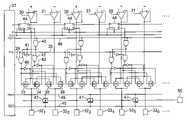
- the semiconductor device of the present inventionis equipped with a test circuit 1 located at the stage following an output buffer that outputs a plurality of output signals.
- the test circuit 1has output buffers 2 1 , 2 2 , . . . , 2 n , output pads 3 1 , 3 2 , . . . , 3 n , output switches 4 1 , 4 2 , . . . , 4 n , a single test pad 5 , interpad (pad-to-pad) switches 6 1 , 6 2 , . . . , 6 n , and a controller 7 .
- the output buffers 2 1 , 2 2 , . . . , 2 nform respective output circuits.
- the output pads 3 1 , 3 2 , . . . , 3 nare connected in series between the output pads 3 1 , 3 2 , . . . , 3 n , and the output buffers 2 1 , 2 2 , . . . , 2 n .
- the interpad switches 6 1 , 6 2 , . . . , 6 nare provided between the adjacent pads 3 1 , 3 2 , . . . , 3 n and between the output pad 3 n and the test pad 5 .
- the controller 7controls the output switches 4 1 , 4 2 , . . . , 4 n and the interpad switches 6 1 , 6 2 , . . . , 6 n .
- the function testis carried out as follows. On the signal input side, the probe pads are brought into contact with all the pads of the input terminals used in the test, and the test signals are input thereto. On the signal output side, only the test pad 5 is brought into contact with the probe needle, and all the output signals available at the output pads 3 1 , 3 2 , . . . , 3 n are detected via the test pad 5 .
- the controller 7 of the test circuitturn OFF all the output switches 4 1 , 4 2 , . . . , 4 n , and simultaneously, turns ON all the interpad switches 6 1 , 6 2 , . . . , 6 n .
- the controller 7sequentially turns ON one of the output switches 4 1 , 4 2 , . . . , 4 n . More particularly, the controller 7 initially turns ON only the output switch 4 1 .
- the output of the output buffer 2 1is electrically connected to the test pad 5 via the output switch 4 1 and all the interpad switches 6 1 , 6 2 , . . . , 6 n .
- the output signal of the output buffer 2 1is output to the test pad 5 .
- the first output switch 4 1is turned OFF and only the second output switch 4 2 is turned ON. This connects the output of the output buffer 2 2 to the test pad 5 via the output switch 4 2 and the interpad switch 6 2 , . . .
- the output signal of the output buffer 2 2is output to the test pad 5 .
- one of the output switches 4 1 , 4 2 , . . . , 4 nis sequentially turned ON, so that the output signals of the output buffers 2 1 , 2 2 , . . . , 2 n can be sequentially output to the test pad 5 one by one.
- the output signal available at the test pad 5is monitored via the single probe needle, so that the outputs of all the output buffers 2 1 , 2 2 , . . . , 2 n , can be tested.
- FIG. 2is a circuit diagram that partially illustrates a structure of the test circuit according to the first embodiment of the present invention
- FIG. 3is a waveform diagram of signals observed in the circuit shown in FIG. 2 .
- An integrated circuit called a source driver or data driver, and another integrated circuit called a gate driverare connected to the liquid crystal panel.
- the circuit shown in FIG. 2is a part of the data driver.
- the final stage of the data driveris an output circuit that supplies each pixel of the liquid crystal panel with an image voltage.
- the output circuitis composed of a plurality of operational amplifiers 10 1 , 10 2 , . . . provided to the respective pixels.
- the output terminals of the operational amplifiers 10 1 , 10 2 , . . .are connected to output pads 12 1 , 12 2 , . . . via transfer gates 11 1 , 11 2 , . . .
- Each transfer gatefunctions as a switch that operates as follows. Each transfer gate is turned OFF when a high-level voltage is applied to the gate terminal of the P-channel MOS transistor, and a low-level voltage is applied to the gate terminal of the N-channel MOS transistor. Each transfer gate is turned ON when the low-level voltage is applied to the gate terminal of the P-channel MOS transistor and the high-level voltage is applied to the gate terminal of the N-channel MOS transistor.
- the gate terminals of the transfer gates 11 1 , 11 2 , . . . on the N-channel sideare connected to non-inverting output terminals of flip-flops 13 1 , 13 2 , . . . , and the gate terminals thereof on the P-channel side are connected to inverting output terminals.
- a data input terminal (D) of the flip-flop 13 1is connected to the controller 14 , and the non-inverting output terminal thereof is connected to a data input terminal of the next flip-flop 13 2 .
- the non-inverting output terminal of the flip-flop 13 2is connected to the data input terminal of the next flip-flop.
- the plurality of flip-flops 13 1 , 13 2 , . . .are cascaded.
- Clock input terminals (CLK) and a reset input terminal (R) of the flip-flops 13 1 , 13 2 , . . .are connected to a clock line 15 and a reset line 16 both connected to the controller 14 .
- Transfer gates 18 1 , 18 2 , . . . that have switching functionsare connected between the adjacent output pads 12 1 , 12 2 , . . . and the output pad arranged at the final stage of the output circuit and a test pad 17 .
- Each of the transfer gatesis made up of a P-channel MOS transistor and an N-channel MOS transistor.
- the gate terminals of the transfer gates 18 1 , 18 2 , . . . on the N-channel sideare connected to a test line 19 on which a non-inverting test signal travels, and gate terminals thereof on the P-channel side are connected to a test line 20 on which an inverting test signal travels.
- the controller 14outputs the reset signal to the reset line 16 to thereby reset all the flip-flops 13 1 , 13 2 , . . . and to turn OFF all the transfer gates 11 1 , 11 2 , . . . , so that all the outputs of the operational amplifiers 10 1 , 10 2 , . . . are in the high-impedance state.
- the controller 14outputs a high-level voltage C and a low-level voltage to the test lines 19 and 20 , respectively, so that all the transfer gates 18 1 , 18 2 , . . . are in the ON state.
- the controller 14outputs a clock signal to the clock line 15 .
- the first flip-flop 13 1latches high-level data output to the controller 14 via the data input terminal in synchronism with the clock signal, and outputs data B at the high level and data at the low level to the non-inverting and inverting output terminals, respectively.
- the transfer gate 11 1is turned ON, and the gradation voltage signal A of the operational amplifier 10 1 is output to the output pad 12 1 .
- the gradation voltage signal Ais output, as an output signal E, to the test pad 17 via all the transfer gates 18 1 , 18 2 , . . .
- the data that is being output to the flip-flop 13 1 , from the controller 14is switched to the low level.
- the flip-flop 13 1latches data at the low level in synchronism with the next clock signal, and sets data B of the non-inverting output terminal to the low level, setting data of the inverting output terminal to the high level.
- the second flip-flop 13 2latches the data at the high level being output to the non-inverting output terminal of the first flip-flop 13 1 , and outputs data D at the high level to the non-inverting output terminal, outputting data at the low level to the inverting output terminal.
- the transfer gate 11 1is turned OFF, and cuts off the gradation voltage signal A of the operational amplifier 10 1 .
- the transfer gate 11 2is switched to ON, and outputs a gradation voltage signal F of the operational amplifier 10 2 to the output pad 12 2 .
- the gradation voltage signal Fis output, as an output signal E, to the test pad 17 via the transfer gates 18 2 , . . .
- the third flip-flop and the remaining flip-flopsequentially latch the output of the previous stage, so that the third transfer gate and the remaining transfer gates are sequentially turned ON.
- the outputs of the operational amplifiersare sequentially output to the test pad 17 one by one. This makes it possible to test all the outputs of the output circuit of the data driver by merely bringing the probe needle to only the test pad 17 without being short-circuited.
- FIG. 4is a circuit diagram that partially shows a structure of the test circuit according to a second embodiment of the present invention.
- the test circuitutilizes a part of the circuit that forms the data driver as a transfer gate that cuts off the operational amplifier that is not to be measured. More particularly, a data driver that drives a liquid crystal panel into which a liquid crystal and a TFT (Thin Film Transistor) are combined a positive-polarity system, a negative-polarity system and a polarity reversing circuit because such a data driver is required to alternately output the gradation voltage positive to the common voltage and the gradation voltage negative thereto.
- the polarity reversing circuitis utilized as a switch that cuts off the output of the operational amplifier that is not to be measured.
- an operational amplifier 30 which outputs a gradation voltage of the positive polarity and an operational amplifier 31 which outputs a gradation voltage of the negative polarityare paired, and a plurality of such pairs are provided.
- the output terminals of the pairs of operational amplifiersare connected to output pads 32 1 , 32 2 , 32 3 , 32 4 , 32 5 , 32 6 , . . . via the polarity reversing circuits.
- Each of the polarity reversing circuitsis made up of four transfer gates 33 , 34 , 35 and 36 , each of which transfer gates is made up of a P-channel MOS transistor and an N-channel MOS transistor.
- the output terminals of the operational amplifiers 30are connected to odd-numbered output pads 32 1 , 32 3 , 32 5 , . . . via the transfer gates 33 , and are connected to even-numbered output pads 32 2 , 32 4 , 32 6 , . . . via the transfer gates 35 .
- the output terminals of the operational amplifiers 31are connected to the odd-numbered output pads 32 1 , 32 3 , 32 5 , via the transfer gates 34 , and are connected to even-numbered output pads 32 2 , 32 4 , 32 6 , . . . via the transfer gates 36 .
- the output terminals of the NAND gates 39are connected to the gate terminals of the transfer gates 33 and 36 on the P-channel side and input terminals of inverters (NOT gates) 40 .
- the output terminals of the inverters 40are connected to the gate terminals of the transfer gates 33 and 36 on the N-channel side.
- the switching control line 38is connected to the first input terminals of the NAND gates 42 via the inverters 41 .
- the output terminals of the NAND gates 42are connected to the gate terminals of the transfer gates 34 and 35 on the P-channel side and the input terminals of the inverters 43 .
- the output terminals of the inverters 43are connected to the gate terminals of the transfer gates 34 and 35 on the N-channel side.
- the controller 37has a data output terminal, a clock signal output terminal and a reset signal output terminal, these terminals being connected to flip-flops 44 .
- the flip-flops 44are cascaded so that the non-inverting output terminals thereof are connected to data input terminals of the next-stage flip-flops 44 .
- the inverting output terminals of the flip-flops 44are connected to the first input terminals of the NAND gates 45 .
- the second input terminals of the NAND gates 45are connected to a test line 46 via which the non-inverting test signal from the controller 37 is transferred.
- the output terminals of the NAND gates 45are connected to the second input terminals of the NAND gates 39 and 42 .
- Transfer gates 47are connected between the odd-numbered output parts 32 1 , 32 3 , 32 5 , . . . and the gate terminals thereof on the N-channel side are connected to a test line 48 via which the non-inverting test signal from the controller 37 is output.
- the gate terminals of the transfer gates 47 on the P-channel sideare connected to a test line 49 via which the inverting signal from the controller 37 is transferred.
- the transfer gate 47 of the final stageis connected to a test pad 50 .
- the controller 37resets all the flip-flops 44 . At that time, the controller 37 outputs a low-level voltage to the test lines 46 , 48 and 49 and the switching control line 38 . Thus, the high-level voltages are output via the output terminals of the NAND gates 45 and 39 , and the low-level voltages are output via the output terminals of the NAND gates 42 . Thus, the transfer gates 33 and 36 are OFF, while the transfer gates 34 and 35 are ON.
- the controller 37When the controller 37 outputs the test signal that is at the high level, the low-level voltages are output via the output terminals of all the NAND gates 45 , and the high-level voltages are output via the output terminals of the NAND gates 39 and 42 . Thus, all the transfer gates 33 , 34 , 35 and 36 of the polarity reversing circuit are OFF, and all the transfer gates 47 connected to the odd-numbered output pads 32 1 , 32 3 , 32 5 and the test pad 50 are ON.
- the controller 37outputs the polarity switching signal POL at the high level.
- the transfer gates 33 and 36 of the polarity reversing circuitto be ON while causing the transfer gates 34 and 35 thereof to be OFF.
- the output of the operational amplifier that outputs the gradation voltage of the positive polarityare connected to the test pad 50 via the transfer gates 33 and 47 , so that the gradation voltage of the positive polarity can be output to the test pad 50 .
- the controller 37when the controller 37 outputs the polarity reversing signal POL of the low level, the states of the output terminals of the NAND gates 39 and 42 are reversed. Therefore, in turn, the transfer gates 33 and 36 of the polarity reversing circuit are OFF, while the transfer gates 34 and 35 are ON.
- the output of the operational amplifier 31 that outputs the gradation voltage of the negative polarityis connected to the test pad 50 via the transfer gates 34 and 47 , so that the gradation voltage of the negative polarity can be output to the test pad 50 .
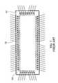
- FIG. 5is a conceptual view of a pad formation surface of an integrated circuit for the data driver.
- An integrated circuit 51has a pad arrangement in which pads for inputting and outputting are arranged along the sides of the shape thereof.
- input pads 52 and a test pad 53are arranged along a side of the integrated circuit 51
- output pads 54are arranged along the remaining three sides.
- the input pads 52 and the test pad 53 to which probe needles 55 are to be contactedare arranged at a pitch approximately equal to the conventional pitch so that no problem will be encountered at the time of contacting the probe needles 55 .
- the output pads 54are arranged at a narrower pitch because the output pads 54 are not brought into contact with the probe needles 55 .
- the output signals that are output to all the output pads 54are tested by the single test pad 53 .
- the output pads 54are divided into some groups for each of which groups the single test pad 53 is provided.
- the single output pad 54is provided for the 48 output pads.
- eight test pads 53are provided for the 384 output pads 54 , and are arranged in the same line as the input pads 52 . The function test is simultaneously carried out for every group, so that the time necessary to carry out the function test can be reduced.
- one side of the integrated circuit 51is occupied by the input pads 52 and the test pad 53 .
- part of the sidemay be used to dispose the output pads 54 .
- FIG. 6is a view that explains how the integrated circuit for the data driver is tested.
- the probe needlesare contacted to the input and output pads along the four sides thereof.
- the input pads and the test padare arranged along the same side. Therefore, two integrated circuits can be simultaneously tested with the conventional test device.
- a plurality of integrated circuits 512are arranged side by side and are transported. In the test positions, every the integrated circuits 51 are fixed in given positions every two circuits, and probe needles 55 arranged in two lines for the input pads 52 and the test pads 53 of the integrated circuit can be contacted and detached simultaneously.
- the probe needles 55are brought into contact with a small number of input pads 52 and the test pad 53 .
- the contract pressureit is possible to easily adjust the contract pressure and achieve stable contacts.
- two integrated circuits 51are simultaneously tested, so that the time necessary for positioning the probe needles and the test time can be reduced.
- the voltages that appear on the output padscan be sequentially output to the single test pad.
- the testcan be carried out using the test pad rather than the output pads, it is possible to reduce the pitch without being restricted by the pitch at which the output pads are arranged. Such narrowing the pitch contributes to reducing the chip area and the cost.
- the testcan be carried out with a number of contacts with the input pads and test pad, so that the contact pressure with which the probe needles are contracted can easily be adjusted and sure contacts can be made.
- the input pads used in the test and the test padare arranged in line, so that the probe needles can be positioned with a reduced time.
- two adjacent integrated circuitscan be tested simultaneously, so that the test can be carried out with a reduced time and the cost can be reduced.
Landscapes
- Engineering & Computer Science (AREA)
- Physics & Mathematics (AREA)
- Computer Hardware Design (AREA)
- General Physics & Mathematics (AREA)
- Theoretical Computer Science (AREA)
- Testing Or Measuring Of Semiconductors Or The Like (AREA)
- Tests Of Electronic Circuits (AREA)
Abstract
Description
Claims (1)
Priority Applications (1)
| Application Number | Priority Date | Filing Date | Title |
|---|---|---|---|
| US11/487,339US7580020B2 (en) | 2001-11-29 | 2006-07-17 | Semiconductor device and liquid crystal panel driver device |
Applications Claiming Priority (2)
| Application Number | Priority Date | Filing Date | Title |
|---|---|---|---|
| JP2001-363617 | 2001-11-29 | ||
| JP2001363617AJP3895163B2 (en) | 2001-11-29 | 2001-11-29 | LCD panel driver |
Related Child Applications (1)
| Application Number | Title | Priority Date | Filing Date |
|---|---|---|---|
| US11/487,339DivisionUS7580020B2 (en) | 2001-11-29 | 2006-07-17 | Semiconductor device and liquid crystal panel driver device |
Publications (2)
| Publication Number | Publication Date |
|---|---|
| US20030098859A1 US20030098859A1 (en) | 2003-05-29 |
| US7098878B2true US7098878B2 (en) | 2006-08-29 |
Family
ID=19173928
Family Applications (2)
| Application Number | Title | Priority Date | Filing Date |
|---|---|---|---|
| US10/205,414Expired - LifetimeUS7098878B2 (en) | 2001-11-29 | 2002-07-26 | Semiconductor device and liquid crystal panel driver device |
| US11/487,339Expired - LifetimeUS7580020B2 (en) | 2001-11-29 | 2006-07-17 | Semiconductor device and liquid crystal panel driver device |
Family Applications After (1)
| Application Number | Title | Priority Date | Filing Date |
|---|---|---|---|
| US11/487,339Expired - LifetimeUS7580020B2 (en) | 2001-11-29 | 2006-07-17 | Semiconductor device and liquid crystal panel driver device |
Country Status (2)
| Country | Link |
|---|---|
| US (2) | US7098878B2 (en) |
| JP (1) | JP3895163B2 (en) |
Cited By (2)
| Publication number | Priority date | Publication date | Assignee | Title |
|---|---|---|---|---|
| US20050122297A1 (en)* | 2003-12-03 | 2005-06-09 | Kengo Imagawa | Semiconductor device and the method of testing the same |
| US20120105093A1 (en)* | 2010-10-29 | 2012-05-03 | Hynix Semiconductor Inc. | Semiconductor apparatus and method of testing and manufacturing the same |
Families Citing this family (18)
| Publication number | Priority date | Publication date | Assignee | Title |
|---|---|---|---|---|
| US7750660B2 (en)* | 2006-03-30 | 2010-07-06 | Qualcomm Incorporated | Integrated circuit with improved test capability via reduced pin count |
| JP4708269B2 (en) | 2006-06-22 | 2011-06-22 | シャープ株式会社 | Semiconductor device and inspection method of semiconductor device |
| JP2008242164A (en)* | 2007-03-28 | 2008-10-09 | Nec Electronics Corp | Driver circuit of display device and test method thereof |
| TWI418906B (en)* | 2009-10-06 | 2013-12-11 | Au Optronics Corp | Display panel with optimum pad layout of the gate driver |
| KR101110818B1 (en) | 2009-12-28 | 2012-02-24 | 주식회사 하이닉스반도체 | Semiconductor integrated circuit |
| KR101036924B1 (en) | 2009-12-28 | 2011-05-25 | 주식회사 하이닉스반도체 | Semiconductor integrated circuit |
| KR20120037053A (en)* | 2010-10-11 | 2012-04-19 | 삼성전자주식회사 | Integrated circuit, test operation method thereof, and apparatus having the same |
| KR20120056017A (en)* | 2010-11-24 | 2012-06-01 | 삼성전자주식회사 | Multi-channel semiconductor device and display device with the same |
| KR20120119532A (en) | 2011-04-21 | 2012-10-31 | 에스케이하이닉스 주식회사 | Semiconductor memory device and test method thereof |
| KR101901869B1 (en)* | 2011-11-10 | 2018-09-28 | 삼성전자주식회사 | A Display Driving Device and A Display System with enhanced protecting function of Electo-Static discharge |
| KR20130066275A (en)* | 2011-12-12 | 2013-06-20 | 삼성전자주식회사 | Display driver and manufacturing method thereof |
| WO2013131071A1 (en)* | 2012-03-02 | 2013-09-06 | Silicon Light Machines Corporation | Driver for mems spatial light modulator |
| KR20170029927A (en) | 2015-09-08 | 2017-03-16 | 에스케이하이닉스 주식회사 | Semiconductor device and semiconductor system |
| JP6655461B2 (en) | 2016-04-28 | 2020-02-26 | ラピスセミコンダクタ株式会社 | Semiconductor device, semiconductor chip, and method of testing semiconductor chip |
| US10818208B2 (en)* | 2018-09-14 | 2020-10-27 | Novatek Microelectronics Corp. | Source driver |
| CN110221491A (en)* | 2019-05-06 | 2019-09-10 | 惠科股份有限公司 | Array substrate, manufacturing method thereof and liquid crystal display panel |
| KR102675921B1 (en)* | 2019-11-07 | 2024-06-17 | 엘지디스플레이 주식회사 | Display Device and method for detecting the data link line defect of the display device |
| KR20240080415A (en)* | 2022-11-30 | 2024-06-07 | 매그나칩믹스드시그널 유한회사 | Display driving IC device and probe test method using the same |
Citations (14)
| Publication number | Priority date | Publication date | Assignee | Title |
|---|---|---|---|---|
| JPH0574898A (en) | 1990-12-27 | 1993-03-26 | Toshiba Corp | Manufacture of semiconductor devices |
| JPH08184646A (en)* | 1994-12-28 | 1996-07-16 | Nec Ic Microcomput Syst Ltd | Semiconductor integrated circuit |
| JPH08248935A (en)* | 1995-03-09 | 1996-09-27 | Fujitsu General Ltd | Image display device |
| US5818252A (en)* | 1996-09-19 | 1998-10-06 | Vivid Semiconductor, Inc. | Reduced output test configuration for tape automated bonding |
| JPH1184420A (en) | 1997-09-09 | 1999-03-26 | Toshiba Corp | Liquid crystal display device, array substrate inspection method, and array substrate tester |
| JPH11149092A (en) | 1997-11-17 | 1999-06-02 | Advanced Display Inc | Liquid crystal display device and its inspection method |
| US5981971A (en)* | 1997-03-14 | 1999-11-09 | Kabushiki Kaisha Toshiba | Semiconductor ROM wafer test structure, and IC card |
| US6028442A (en)* | 1996-04-24 | 2000-02-22 | Samsung Electronics, Co., Ltd. | Test circuit for identifying open and short circuit defects in a liquid crystal display and method thereof |
| JP2000056741A (en) | 1998-06-03 | 2000-02-25 | Fujitsu Ltd | Liquid crystal panel drive circuit and liquid crystal display device |
| JP2000208717A (en) | 1999-01-19 | 2000-07-28 | Sharp Corp | Semiconductor chip and semiconductor device package, and probe card and package test method |
| JP2001056664A (en) | 1999-08-19 | 2001-02-27 | Fujitsu Ltd | LCD panel drive circuit |
| US6304241B1 (en)* | 1998-06-03 | 2001-10-16 | Fujitsu Limited | Driver for a liquid-crystal display panel |
| US6335721B1 (en)* | 1998-03-27 | 2002-01-01 | Hyundai Electronics Industries Co., Ltd. | LCD source driver |
| US20030034941A1 (en)* | 2001-08-16 | 2003-02-20 | Philips Electronics North America Corporation | Self-calibrating image display device |
Family Cites Families (4)
| Publication number | Priority date | Publication date | Assignee | Title |
|---|---|---|---|---|
| JPH03127846A (en) | 1989-10-13 | 1991-05-30 | Fuji Electric Co Ltd | Integrated circuit device |
| EP0801401B1 (en)* | 1996-04-02 | 2003-08-27 | STMicroelectronics, Inc. | Testing and repair of embedded memory |
| US6199182B1 (en)* | 1997-03-27 | 2001-03-06 | Texas Instruments Incorporated | Probeless testing of pad buffers on wafer |
| JP2000315771A (en) | 1999-04-30 | 2000-11-14 | Seiko Epson Corp | Semiconductor integrated circuit |
- 2001
- 2001-11-29JPJP2001363617Apatent/JP3895163B2/ennot_activeExpired - Fee Related
- 2002
- 2002-07-26USUS10/205,414patent/US7098878B2/ennot_activeExpired - Lifetime
- 2006
- 2006-07-17USUS11/487,339patent/US7580020B2/ennot_activeExpired - Lifetime
Patent Citations (14)
| Publication number | Priority date | Publication date | Assignee | Title |
|---|---|---|---|---|
| JPH0574898A (en) | 1990-12-27 | 1993-03-26 | Toshiba Corp | Manufacture of semiconductor devices |
| JPH08184646A (en)* | 1994-12-28 | 1996-07-16 | Nec Ic Microcomput Syst Ltd | Semiconductor integrated circuit |
| JPH08248935A (en)* | 1995-03-09 | 1996-09-27 | Fujitsu General Ltd | Image display device |
| US6028442A (en)* | 1996-04-24 | 2000-02-22 | Samsung Electronics, Co., Ltd. | Test circuit for identifying open and short circuit defects in a liquid crystal display and method thereof |
| US5818252A (en)* | 1996-09-19 | 1998-10-06 | Vivid Semiconductor, Inc. | Reduced output test configuration for tape automated bonding |
| US5981971A (en)* | 1997-03-14 | 1999-11-09 | Kabushiki Kaisha Toshiba | Semiconductor ROM wafer test structure, and IC card |
| JPH1184420A (en) | 1997-09-09 | 1999-03-26 | Toshiba Corp | Liquid crystal display device, array substrate inspection method, and array substrate tester |
| JPH11149092A (en) | 1997-11-17 | 1999-06-02 | Advanced Display Inc | Liquid crystal display device and its inspection method |
| US6335721B1 (en)* | 1998-03-27 | 2002-01-01 | Hyundai Electronics Industries Co., Ltd. | LCD source driver |
| JP2000056741A (en) | 1998-06-03 | 2000-02-25 | Fujitsu Ltd | Liquid crystal panel drive circuit and liquid crystal display device |
| US6304241B1 (en)* | 1998-06-03 | 2001-10-16 | Fujitsu Limited | Driver for a liquid-crystal display panel |
| JP2000208717A (en) | 1999-01-19 | 2000-07-28 | Sharp Corp | Semiconductor chip and semiconductor device package, and probe card and package test method |
| JP2001056664A (en) | 1999-08-19 | 2001-02-27 | Fujitsu Ltd | LCD panel drive circuit |
| US20030034941A1 (en)* | 2001-08-16 | 2003-02-20 | Philips Electronics North America Corporation | Self-calibrating image display device |
Non-Patent Citations (4)
| Title |
|---|
| Japanese Patent Office Action issued Jan. 31, 2006 with relevant portions of the Office Action translated. |
| Partial translation of Japanese Office Action issued May 16, 2006. |
| Patent Abstracts of Japan, Publication No. 03-127846; publication date May 30, 1991. |
| Patent Abstracts of Japan, Publication No. 2000-315771; publication date Nov. 14, 2000. |
Cited By (4)
| Publication number | Priority date | Publication date | Assignee | Title |
|---|---|---|---|---|
| US20050122297A1 (en)* | 2003-12-03 | 2005-06-09 | Kengo Imagawa | Semiconductor device and the method of testing the same |
| US7443373B2 (en)* | 2003-12-03 | 2008-10-28 | Renesas Technology Corp. | Semiconductor device and the method of testing the same |
| US20120105093A1 (en)* | 2010-10-29 | 2012-05-03 | Hynix Semiconductor Inc. | Semiconductor apparatus and method of testing and manufacturing the same |
| US8823409B2 (en)* | 2010-10-29 | 2014-09-02 | SK Hynix Inc. | Semiconductor apparatus and method of testing and manufacturing the same |
Also Published As
| Publication number | Publication date |
|---|---|
| US20030098859A1 (en) | 2003-05-29 |
| JP3895163B2 (en) | 2007-03-22 |
| US7580020B2 (en) | 2009-08-25 |
| JP2003163246A (en) | 2003-06-06 |
| US20060256052A1 (en) | 2006-11-16 |
Similar Documents
| Publication | Publication Date | Title |
|---|---|---|
| US7580020B2 (en) | Semiconductor device and liquid crystal panel driver device | |
| KR100437947B1 (en) | A liquid crystal display device | |
| US7098882B2 (en) | Bidirectional shift register shifting pulse in both forward and backward directions | |
| US6201523B1 (en) | Flat panel display device | |
| KR100608106B1 (en) | LCD and source line repair method having a source line repair function | |
| US6982706B1 (en) | Liquid crystal driving circuit, semiconductor integrated circuit device, reference voltage buffering circuit, and method for controlling the same | |
| JP2004212939A (en) | Bidirectional driving circuit and driving method for flat panel display device | |
| KR20020069661A (en) | Circuit for bi-directional driving liquid crystal display panel | |
| US10013931B2 (en) | Liquid crystal display device and pixel inspection method therefor | |
| US7548079B2 (en) | Semiconductor device including analog voltage output driver LSI chip having test circuit | |
| JPH0786526B2 (en) | Multi-mode test equipment | |
| KR20040053584A (en) | Circuit for bi-directional driving liquid crystal display panel | |
| US6630930B2 (en) | Drive circuit and display unit for driving a display device and portable equipment | |
| US20110148842A1 (en) | Source driver for liquid crystal display panel | |
| JP2005189834A (en) | Semiconductor device and its testing method | |
| CN101320548A (en) | Drive circuit and control method of display unit separating amplifier and output | |
| JP5254525B2 (en) | Display device drive circuit | |
| JPH10104568A (en) | Display driver | |
| KR100437624B1 (en) | Semiconductor circuit in which power consumption is reduced and semiconductor circuit system using the same | |
| US8330752B2 (en) | Data line driving circuit, driver IC and display apparatus | |
| US8368635B2 (en) | Source driver for liquid crystal display panel | |
| TWI863365B (en) | Switching circuit for parallel chip testing and chip testing system including the same | |
| CN119479514A (en) | Display device | |
| US20240177640A1 (en) | Display driving ic device and probe test method using the same | |
| JP2007240459A (en) | Display driver, operation method of display driver, program, and computer-readable recording medium |
Legal Events
| Date | Code | Title | Description |
|---|---|---|---|
| AS | Assignment | Owner name:FUJITSU LIMITED, JAPAN Free format text:ASSIGNMENT OF ASSIGNORS INTEREST;ASSIGNORS:UDO, SHINYA;KUMAGAI, MASAO;KOKUBUN, MASATOSHI;AND OTHERS;REEL/FRAME:013134/0651 Effective date:20020531 | |
| STCF | Information on status: patent grant | Free format text:PATENTED CASE | |
| FEPP | Fee payment procedure | Free format text:PAYOR NUMBER ASSIGNED (ORIGINAL EVENT CODE: ASPN); ENTITY STATUS OF PATENT OWNER: LARGE ENTITY | |
| AS | Assignment | Owner name:FUJITSU MICROELECTRONICS LIMITED, JAPAN Free format text:ASSIGNMENT OF ASSIGNORS INTEREST;ASSIGNOR:FUJITSU LIMITED;REEL/FRAME:021998/0645 Effective date:20081104 Owner name:FUJITSU MICROELECTRONICS LIMITED,JAPAN Free format text:ASSIGNMENT OF ASSIGNORS INTEREST;ASSIGNOR:FUJITSU LIMITED;REEL/FRAME:021998/0645 Effective date:20081104 | |
| FPAY | Fee payment | Year of fee payment:4 | |
| AS | Assignment | Owner name:FUJITSU SEMICONDUCTOR LIMITED, JAPAN Free format text:CHANGE OF NAME;ASSIGNOR:FUJITSU MICROELECTRONICS LIMITED;REEL/FRAME:024982/0245 Effective date:20100401 | |
| AS | Assignment | Owner name:SPANSION LLC, CALIFORNIA Free format text:ASSIGNMENT OF ASSIGNORS INTEREST;ASSIGNOR:FUJITSU SEMICONDUCTOR LIMITED;REEL/FRAME:031205/0461 Effective date:20130829 | |
| FPAY | Fee payment | Year of fee payment:8 | |
| AS | Assignment | Owner name:MORGAN STANLEY SENIOR FUNDING, INC., NEW YORK Free format text:SECURITY INTEREST;ASSIGNORS:CYPRESS SEMICONDUCTOR CORPORATION;SPANSION LLC;REEL/FRAME:035240/0429 Effective date:20150312 | |
| AS | Assignment | Owner name:CYPRESS SEMICONDUCTOR CORPORATION, CALIFORNIA Free format text:ASSIGNMENT OF ASSIGNORS INTEREST;ASSIGNOR:SPANSION, LLC;REEL/FRAME:036039/0001 Effective date:20150601 | |
| MAFP | Maintenance fee payment | Free format text:PAYMENT OF MAINTENANCE FEE, 12TH YEAR, LARGE ENTITY (ORIGINAL EVENT CODE: M1553) Year of fee payment:12 | |
| AS | Assignment | Owner name:MUFG UNION BANK, N.A., CALIFORNIA Free format text:ASSIGNMENT AND ASSUMPTION OF SECURITY INTEREST IN INTELLECTUAL PROPERTY;ASSIGNOR:MORGAN STANLEY SENIOR FUNDING, INC.;REEL/FRAME:050896/0366 Effective date:20190731 | |
| AS | Assignment | Owner name:MORGAN STANLEY SENIOR FUNDING, INC., NEW YORK Free format text:CORRECTIVE ASSIGNMENT TO CORRECT THE 8647899 PREVIOUSLY RECORDED ON REEL 035240 FRAME 0429. ASSIGNOR(S) HEREBY CONFIRMS THE SECURITY INTERST;ASSIGNORS:CYPRESS SEMICONDUCTOR CORPORATION;SPANSION LLC;REEL/FRAME:058002/0470 Effective date:20150312 | |
| AS | Assignment | Owner name:SPANSION LLC, CALIFORNIA Free format text:RELEASE BY SECURED PARTY;ASSIGNOR:MUFG UNION BANK, N.A.;REEL/FRAME:059410/0438 Effective date:20200416 Owner name:CYPRESS SEMICONDUCTOR CORPORATION, CALIFORNIA Free format text:RELEASE BY SECURED PARTY;ASSIGNOR:MUFG UNION BANK, N.A.;REEL/FRAME:059410/0438 Effective date:20200416 |