US7098801B1 - Using bitmasks to provide visual indication of operational activity - Google Patents
Using bitmasks to provide visual indication of operational activityDownload PDFInfo
- Publication number
- US7098801B1 US7098801B1US11/168,720US16872005AUS7098801B1US 7098801 B1US7098801 B1US 7098801B1US 16872005 AUS16872005 AUS 16872005AUS 7098801 B1US7098801 B1US 7098801B1
- Authority
- US
- United States
- Prior art keywords
- bitmask
- indicator
- visual indicator
- rate
- relation
- Prior art date
- Legal status (The legal status is an assumption and is not a legal conclusion. Google has not performed a legal analysis and makes no representation as to the accuracy of the status listed.)
- Expired - Fee Related
Links
Images


Classifications
- G—PHYSICS
- G06—COMPUTING OR CALCULATING; COUNTING
- G06F—ELECTRIC DIGITAL DATA PROCESSING
- G06F11/00—Error detection; Error correction; Monitoring
- G06F11/30—Monitoring
- G06F11/32—Monitoring with visual or acoustical indication of the functioning of the machine
- G06F11/324—Display of status information
- G06F11/325—Display of status information by lamps or LED's
Definitions
- the claimed inventionrelates generally to the field of electronic devices and more particularly, but not by way of limitation, to an apparatus and method for providing a visual indication to a user to indicate a level of operational activity of a device.
- Visual indicatorsare used in a variety of electronic devices. Such indicators advantageously convey useful information to the user with regard to a particular state of the device.
- a personal computercan utilize a light emitting diode (LED) that is mounted to the front of a computer case.
- the LEDis “lit” when the computer system is on, indicating a health status of the device (e.g., power is being applied, the system is active, etc.).
- the LEDcan also be configured to intermittently flash when particular activities are taking place, such as a transfer of data between an operational memory space (e.g., system RAM) and a data storage device (e.g., an internally mounted hard disc drive).
- Visual indicatorscan also be used to identify the presence of one or more queued messages for a cellular phone, to signify a power charge/discharge state for a digital camera or other portable device, etc.
- Preferred embodiments of the present inventionare generally directed to an apparatus and method for providing a visual indication of operational activity of a device.
- a pattern generatorprovides one or more bitmasks.
- Each bitmaskcomprises a selected multi-bit sequence of logical values, and corresponds to a selected operational activity of the device such as a power-on state or a selected data transfer operation.
- a switching circuitselectively activates a visual indicator, such as a light emitting diode (LED), to provide a different visual indication in relation to each bitmask.
- a visual indicatorsuch as a light emitting diode (LED)
- the rate at which the visual indicator is selectively activatedis a time-varying rate that is different from a rate of activation of the indicator as perceived by a human observer.
- the pattern generatoris preferably implemented as a programming routine resident in a memory space and executed by a processor.
- the pattern generatoris preferably implemented in hardware, such as through the use of an index table and shift register circuitry.
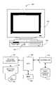
- FIG. 1is an elevational representation of a personal computer (PC) workstation constructed and operated in accordance with preferred embodiments of the present invention.
- PCpersonal computer
- FIG. 2is a simplified functional block diagram of the workstation of FIG. 1 .
- FIG. 3shows an exemplary bitmask provided by the pattern generator of FIG. 2 that activates the visual indicator of FIG. 2 at a time-varying rate.
- FIG. 4shows relevant aspects of the pattern generator and switching circuit of FIG. 2 in accordance with a preferred hardware embodiment.
- FIG. 5provides another preferred construction for the circuit of FIG. 2 in which multiple activity levels are concurrently indicated.
- FIG. 6provides an alternative preferred construction to the circuit shown in FIG. 5 .
- FIG. 7provides yet another preferred construction for the circuit of FIG. 4 .
- FIG. 8generally represents a preferred format for the index table of FIG. 4 .
- FIG. 1depicts a personal computer (PC) workstation 100 of the type used to carry out PC related tasks.
- the workstation 100can be a stand-alone computer, can be linked to a local area or wide area network, can be a controller in a large capacity data storage array system that communicates with remote systems via a fabric (such as the Internet), etc.
- a fabricsuch as the Internet
- the workstation 100includes a number of features and capabilities that are well known to the reader and thus further discussion thereof is omitted for brevity. It is sufficient for the present purposes to point out a case (housing) 102 , and a monitor display 104 of the LCD variety.
- the case 102preferably houses a number of components such as including those depicted in FIG. 2 .
- a central processing unit (CPU) 106provides central communication and control functions for the workstation 100 , and is preferably mounted on a motherboard (not separately shown). During operation the CPU 106 accesses system memory 108 , preferably characterized as a volatile memory space (RAM).
- RAMvolatile memory space
- a controller card 110preferably plugs into the motherboard to facilitate communication between the CPU 106 and an internally mounted data storage device 112 .
- the device 112will be contemplated as comprising a hard disc drive which magnetically stores and retrieves data to and from one or more rigid rotatable data storage discs.
- FIG. 2further shows a pattern generator 114 in communication with the CPU 106 .
- the pattern generator 114can be realized in hardware or firmware; that is, as a hard-wired logic circuit disposed on the motherboard, as a processing module of the programming stored in MEM 108 and carried out by the CPU 106 , or a combination of both, as desired.
- a switching circuit 116controls a visual indicator 118 .
- the switching circuit 116is preferably realized in hardware, and the visual indicator 118 is preferably characterized as a light emitting diode (LED) mounted to the front of the case 102 ( FIG. 1 ) for ready perception by a user of the workstation 100 .
- LEDlight emitting diode
- the pattern generator 114preferably operates to output bitmasks to the switching circuit 116 , which in turn selectively activates and deactivates the visual indicator 118 in relation thereto.
- Each bitmaskpreferably comprises a unique multi-bit pattern sequence of logical 0's and logical 1's to communicate activity information to the user.
- the rate at which the visual indicator is activated by the switching circuit 116 in response to each bitmaskis a selected time-varying rate (i.e., variable with respect to time), such as depicted in FIG. 3 .
- This applied time-varying rateis selected to be different from a rate of activation of the indicator 118 as perceived by the human observer.
- the bitmaskscorrespond to different operational activities of the system, such as I/O transfers, that are not associated with operation of the visual indicator 118 .
- the visual indicatoris characterized as a secondary indicator of a separate ongoing activity, rather than being the primary activity itself such as operation of a display device (e.g., 104 ) to provide image data.
- the pattern generator 114is preferably implemented in software (e.g., a routine executed by the CPU 106 ), but can alternatively be implemented in hardware that utilizes command inputs from the CPU 106 , as desired. Preferred exemplary implementations using software and hardware will be presented below.
- activity levelscan be indicated by the intensity (brightness) of the indicator. This can be implemented by physically changing the intensity of the indicator in a number of ways.
- the indicatorwhen the indicator has the capability of being at several intensities (such as an incandescent device), the indicator can be set to a given intensity level by setting the applied voltage and/or current to an appropriate steady-state level.
- the indicatorwhen the indicator has the capability of being at several intensities (such as an incandescent device), the indicator can be set to a given intensity level by setting the applied voltage and/or current to an appropriate steady-state level.
- the indicatorwhen the indicator has generally only two levels of intensity (on and off, such as with an LED), the indicator can be turned on and off in rapid succession and at various intervals to provide the desired intensity.
- Thiscan be implemented using a specialized hardware circuit or computer software that operates to toggle the state of the indicator at a rate higher than the rate of human flicker perception.
- the associated CPUwill generally need to devote a significant number of CPU cycles to turning the indicator on and off at such rate. In many systems this can present an unacceptably high overhead burden on the CPU, as the CPU is required to provide other system tasks.
- preferred embodiments of the present inventionpreferably utilize temporal dithering techniques to indicate activity at a much lower duty cycle or “flicker” rate, resulting significantly reducing processing overhead/hardware complexity.
- the indicatorhas a variable intensity. It will be contemplated that a minimum intensity (distinguishable from “off”) at which a typical observer could see a variable intensity LED is Imin (e.g. this might be 20% of the LED minimum brightness). The maximum intensity at which the observer could see a variable intensity LED is contemplated to be Imax (e.g 100% of the LED's maximum brightness).
- the intensitycan be selected to change at a rate higher than the observer's perception rate. This latter rate is defined as Tpnf (“Time Perceived No Flicker” in milliseconds, ms).
- TpnfTime Perceived No Flicker
- msmilliseconds
- SpnfSwitchched Perceived No Flicker
- the peripheral vision of a typical observercan detect around 60 Hz flicker, so an exemplary selected flicker rate Spnf will be 72 Hz, with a corresponding Tpnf of 13.888 ms.
- the rate of change of intensityshould be changed less often than the observer's perception rate so that the indicator appears to flicker, but more often than a rate at which the indicator appears to provide merely a blink.
- This ratewill be defined as Tf (in ms) and Sf (Hz).
- the flicker ratemay be changed on the order of 10 to 20 times a second. Nevertheless, this would still require a significant amount of CPU overhead, and far more than what would be desired or available for dedication to this operation.
- temporal ditheringthat is dithering in the temporal space.
- Such temporal ditheringis preferably enacted herein based on a supposition that if the required update rate is low, exact representation of the actual activity level may not be achievable, only approximated. However, it is contemplated that such approximation will be sufficient to convey the necessary information to the observer.
- temporal ditheringis implemented herein using a total of Nli*Nli bitmasks (masks), where every mask set has Nli bits.
- a different mask setis used for each desired intensity level.
- a different mask setis further used for each instance to avoid a steady “flashing appearance.” When a certain intensity value (Iv) is picked up, the next bit will be chosen in the appropriate mask.
- Listing 1is embodied as the pattern generator 114 of FIG. 2 and is executed by the CPU 106 .
- the bitmasks generated by Listing 1will have various permutations.
- the bit level for the lowest intensity (1 out of 8 bits on in this example)might be:
- the routinepreferably uses a variable pattern to simulate an intensity level. By altering the pattern, no static flicker pattern is present, and thus the indicator 118 does not appear to be “blinking” at a constant rate. Constant blinking can often be confused with conveying a “state” rather than an activity level (e.g., similar to a “busy signal” on a phone). Constant repetitious lights thus generally convey different messages than variable flickering.
- Listing 1can be readily modified as required depending on the requirements of a given application.
- many of the variables in the listingcould be instead assigned fixed values.
- the key valuescould be selected to be powers of 2 to replace the various multiply and divide operations into shift+ addition operations.
- state informationis also conveyed to the observer.
- State informationin this context relates to some characteristic state of the device, such as health (e.g., “power status”).
- no light from the indicator 118corresponds to a state of no power (i.e., the system 100 is turned off).
- some level of indicationgenerally needs to be conveyed by the indicator 118 .
- the indicator 118should display a solid light of given intensity (i.e., no flashing/flickering).
- a solid light of given intensityi.e., no flashing/flickering.
- Listing 2is preferably characterized as the pattern generator 114 of FIG. 2 in the form of a software module executed by the CPU 106 .
- this routinewill display a solid LED light when no activity is occurring, and will always display a minimum intensity when power is applied to the system 100 .
- Both Listing 1 and Listing 2serve to activate the indicator 118 to provide a different visual indication to the observer in relation to each of a plurality of different operational activities (as well as different states for Listing 2). Furthermore, the varying rate of activation of the indicator is significantly different than the rate of activation as perceived by the observer.
- precisely placed and sized pulses(such as from Listings 1, 2) occurring as few as 8 to 10 per second can be perceived as a continuously “on” indication.
- the observercan perceive flickering at a high rate that is, in fact, induced by a significantly lower actual activation rate.
- the routines discussed aboveadvantageously require significantly reduced CPU overhead as compared to a real time implementation where the perceived rate is the same as the actually applied rate.
- FIG. 4shows relevant portions of the pattern generator 114 and the switching circuit 116 in accordance with a preferred hardware construction.
- the hardwareoperates to receive top level activity (and state) indication signals from CPU 106 (or other source), and in response thereto, provide the appropriate bitmasks to activate the indicator in a manner as set forth above.
- the hardwareincludes an index table 120 that receives an activity level input from the CPU 106 related to a then-current state of the workstation 100 . In response to the activity level input, the index table outputs an associated bitmask to a shift register 122 .
- Each bit in the bitmaskis sequentially output by the shift register 122 on path 124 at a rate controlled by an input clock 126 .
- the shift registeris preferably of the “ring” variety so that each output bit is appended to the end of the sequence, as represented by path 128 . In this way, once a selected bitmask is loaded into the shift register 122 , the shift register operates to automatically sequence through the bit pattern over and over again. This operation will continue until a new pattern is loaded by the index table 120 , or further operation of the register is otherwise interrupted.
- a switching device 130is disposed between a reference voltage (VREF) source 132 , the LED 118 , and a reference line 134 .
- the VREF voltageis preferably a suitable positive voltage such as +5 VDC, and the reference voltage is preferably ground (substantially 0 VDC).
- the switching device 130preferably comprises an n-type metal oxide semiconductor field effect transistor (MOSFET) with gate terminal coupled to path 124 , source terminal coupled to the VREF source 132 and drain terminal coupled to reference line 134 .
- MOSFETmetal oxide semiconductor field effect transistor
- a logical 1 input to the MOSFET from path 124closes the circuit and activates the LED
- a logical 0 input from path 124opens the circuit and deactivates the LED.
- Other configurationscan readily be used, however, including multi-pixel visual indicators.
- bitmasksare provided by the index table 120 , with a different mask for each activity level.
- the respective bitmaskscan be empirically determined and adapted as desired.
- the various bitmasksprovide different perceived brightness levels to the user with little or no flickering. This can be readily accomplished through temporal dithering; that is, selecting the cycle rate at a sufficient level so that the user perceives the LED 118 to be more-or-less continuously “on.” Depending on the characteristics of the system, a cycle rate of as little as 8 or 10 cycles per second may be sufficient to establish such perceived “steady state” operation of the LED 118 .
- temporal ditheringcan be utilized to activate and deactivate the LED 118 for each bitmask at a rate that is selected to be different from the rate perceived by the user.
- the cycling of the LED 118is faster than that perceived by the user, but in other embodiments, the rate may be slower.
- the bitmasks from the index table 120can provide both brightness levels and flickering perceptions for at least selected ones, or all of the bitmasks.
- activity level 1exhibit an effective, relatively low steady state brightness with a relatively high rate of flickering
- activity level 3is brighter and has a perceived relatively low flickering rate.
- temporal ditheringresults in activation rates of the LED 118 that are different from the rates perceived by the user.
- FIG. 5provides another preferred hardware embodiment for the pattern generator 114 in which an index table 170 receives two different activity level inputs from the CPU 106 (paths 172 and 174 ). The table 170 outputs an associated bitmask in relation to the two selected inputs. As in FIG. 4 , the output bitmask is supplied to shift register circuitry 176 , which activates and deactivates the switch 130 .
- a unique bitmaskcan be pre-selected for each possible combination of the inputs, which results in the two activity levels combining to locate the unique “address” of the corresponding bitmask within the table 170 . This allows the use of a relatively straightforward look-up approach, although the size of the table will need to be increased to accommodate the resulting larger population of entries.
- each activitycan access a separate portion of the index table, as denoted by INDEX 1 and INDEX 2 blocks 180 , 182 .
- the respective outputs of these blocksconstitute first and second bitmasks, which are combined by a suitable logical operator (such as an exclusive-OR, XOR block 188 ) to provide a final output bitmask on path 190 .
- a suitable logical operatorsuch as an exclusive-OR, XOR block 188
- bitmasks in the various embodiments discussed aboveare preferably predetermined, with greater levels of complexity in the numbers and types of indications made, in some applications it may be possible to arrive at a sequence that at least periodically appears to a typical user to not indicate activity, but rather that the device has no power, that the desired activity is not in fact taking place, etc.
- FIG. 7provides yet another alternative embodiment to the circuitry of FIG. 4 .
- the bitmask from path 190is preferably supplied to a ring shift register 192 , which is clocked as before to sequentially output the individual bit values from the bitmask on path 194 .
- These bit valuesare presented as an input to a suitable logical operator (such as OR gate 196 ) as well as to the reset (RST) input of a programmable counter 198 .
- the counter 198further receives as an input a threshold value from set block 200 , and the output of the counter 198 supplies a second input to the OR gate 196 via path 202 .
- the counteris reset with each logical 1 on path 194 , and initiates counting up to the threshold value supplied by block 200 . If this value is reached, the counter 198 outputs a logical 1 on path 202 , which inserts a 1 in the final control stream provided to the switch 130 . In this way, a run length limited encoding mechanism can be enacted to provide a maximum allowable number of consecutive logical 0's in the values on path 194 (i.e., a maximum allowable “off” time, as in Listing 2). Additional latching can be supplied as desired to provide a minimum on-pulse width, and similar run length encoding can be added to limit the maximum number of consecutive logical 1's.
- Another advantage of the circuit of FIG. 7is the ability to adaptively adjust the threshold of block 200 , which can be carried out at the user level and/or during manufacturing.
- a set of base bitmaskscan be formulated for a variety of different devices, allowing differences in LED characteristics and other factors to be adaptively compensated, as desired.
- the index tablecan be characterized as an encoder to output a desired bitmask sequence in relation to the input selection signals provided thereto.
- a basic organization of a selected tablemight be arranged as represented in FIG. 8 , so that for each activity level, different values of beam intensity and/or flash rate can be assigned, from which unique bitmask sequences can then be derived to exhibit the desired characteristics.
- bitmaskshave been described as being related to specific activities and are thus respectively loaded without regard to what was previously displayed, in other embodiments it may be desirable to combine multiple bitmasks as sequential activities are selected.
- an existing bitmask supplied to the shift register circuitrymay be modified by a new bitmask for the new activity, so that different patterns are provided to the user in relation to the sequence of activities carried out by the device.
- preferred embodiments of the present inventionare generally directed to an apparatus and method for providing a visual indication of operational activity of a device (such as 100 ).
- a pattern generator(such as 114 ) provides one or more bitmasks.
- Each bitmaskpreferably comprises a selected multi-bit sequence of logical values, and corresponds to a selected operational activity of the device not associated with a visual indicator (such as 118 ).
- a switching circuitselectively activates the visual indicator to provide a different visual indication in relation to each bitmask.
- the visual indicatorcomprises a single light emitting diode (LED).
- the time-varying rate at which the visual indicator is activated and deactivated by the switching circuit in response to each bitmaskis selected to be different from a rate, as perceived by a human observer, of activation and deactivation of the indicator.
- the pattern generatorcan be implemented in software (such as Listing 1, 2) or hardware ( FIGS. 4–7 ).
- the pattern generatoris preferably characterized as a routine executed by a CPU (such as 106 ).
- the pattern generatorpreferably comprises an index table (such as 120 , 170 , 180 , 182 ), which stores each of the bitmasks in turn, and which is accessed in relation to the then-selected operational activity.
- the pattern generatorfurther preferably comprises shift register circuitry (such as 122 , 176 , 192 ) which outputs the logical values of the bitmask to the switching circuit.
- the pattern generatorfurther preferably outputs a first bitmask in relation to a first operational activity (such as by 180 ), outputs a second bitmask in relation to a second operational activity (such as by 182 ), and outputs a final output bitmask (such as by 188 ) to control the visual indicator in relation to the first and second bitmasks.
- time-varying ratewill be understood consistent with the foregoing discussion to describe a rate that varies with respect to time, including but not limited to different effective lengths of pulses and/or different elapsed time between successive pulses.
Landscapes
- Engineering & Computer Science (AREA)
- Theoretical Computer Science (AREA)
- Quality & Reliability (AREA)
- Physics & Mathematics (AREA)
- General Engineering & Computer Science (AREA)
- General Physics & Mathematics (AREA)
- Control Of Indicators Other Than Cathode Ray Tubes (AREA)
Abstract
Description
Utp=(Ntp/IOmax)*Spnf (1)
Setting Itp as “Intensity This Period,” then:
Itp=Utp*(Imax−Imin) (2)
Setting Itpr as “Intensity This Period Ranged,” then:
Itpr=Int(Itp*Nli)/Nli (3)
This provides an Litp (“LED Intensity This Period) of:
Litp=Itrp+Imin (4)
If a flickering indicator is desired, Sf can be substituted in place of Spnf in equation (1). For the following discussion, a flickering indicator will be contemplated as being desired.
| extern uchar | NliMasks[8] [8]; |
| int | NliPos[8], |
| int | LedOnOffCount = 0; |
| int | NoIoStateCount = 0; |
| //Assume that this is called Sf times a second. |
| DisplayLed( ) |
| { |
| NumIOsDone = | CallStaticsRoutineToFigureOutActivity( ); | |
| Vtp = | NumIOsDone/Iomax * Sf; | |
| Itp = | Vtp * (Imax–Imin); | |
| Itpr = | Int (Itp * Nli)/Nli; | |
| Iv = | Itpr; // This is simply an index into the mask. |
| // Bump the dither bit position |
| DitherBit = | NliPos[Iv]++; | |
| DitherMaskIndex = | (DitherBit >> 3) & 7; | |
| //In actuality, DitherMaskIndex = | (DitherBit / Nli) % Nli |
| DitherBit & = 7; | |
| BitOnOrOff = NliMasks[Iv] [DitherMaskIndex] & (1 << DitherBit); | |
| if (BitOnOrOff) | |
| { |
| TurnOnTheLed( ), //Additional features can be added as |
| desired to prevent turning on an already turned on LED. |
| } | |
| else | |
| { |
| Turn OffTheLed( ); |
| } | |
| return; |
| } |
| extern uchar | NliMasks[8] [8]; |
| int | NliPos[8], |
| int | LedOnOffCount = 0; |
| int | NoIoStateCount = 0; |
| // Assume that this is called Sf times a second. |
| DisplayLed( ) |
| { |
| NumIOsDone = CallStaticsRoutineToFigureOutActivity( ); | |
| // A special case check is inserted here. This will allow previous | |
| operation to settle down before assuming steady state. | |
| If (NumIOsDone == 0) | |
| { |
| if (InNoIoState) |
| return, |
| if(++NoIoStateCount >= Si * Tf) | |
| { |
| InNoIoState = | TRUE; | |
| NoIoStateCount = | 0; | |
| TurnOnLed(); | ||
| LedOnOffCount = | Ti * Sf; | |
| Return; |
| } |
| } |
| InNoIoState = | FALSE; | |
| Vtp = | NumIOsDone/Iomax * Sf; | |
| Itp = | Vtp * (Imax−Imin); | |
| Itpr = | Int(Itp * Nli) / Nli; | |
| Iv = | Itpr; // This is simply an index into the mask. |
| // Bump the dither bit position |
| DitherBit = | NliPos[Iv]++; | |
| DitherMaskIndex = | (DitherBit >> 3) & 7; |
| // In actuality, DitherMaskIndex = (DitherBit / Nli) % Nli | |
| DitherBit & = 7; | |
| BitOnOrOff = NliMasks[Iv] [DitherMaskIndex] & (1 << DitherBit); | |
| if (BitOnOrOff) | |
| { |
| // If the bit has been on too long, it will look solid. Turn it off | |
| if(++LedOnOffCount > Ti * Sf) | |
| { |
| LedOn OffCount = 0; | |
| TurnOffTheLed( ); |
| } | |
| else | |
| { |
| TurnOnTheLed( ), // Additional features can be added as |
| desired to prevent turning on an already turned on LED. | |
| } |
| } | |
| else | |
| { |
| if(--LedOnOffCount <0 −Ti * Sf) | |
| { |
| // LED has been off too long. Turn it on. | |
| LedOnOffCount = 0; | |
| TurnOnTheLed( ); |
| } | |
| else | |
| { |
| TurnOffTheLed( ); |
| } |
| return; |
| } |
Claims (20)
Priority Applications (1)
| Application Number | Priority Date | Filing Date | Title |
|---|---|---|---|
| US11/168,720US7098801B1 (en) | 2005-06-28 | 2005-06-28 | Using bitmasks to provide visual indication of operational activity |
Applications Claiming Priority (1)
| Application Number | Priority Date | Filing Date | Title |
|---|---|---|---|
| US11/168,720US7098801B1 (en) | 2005-06-28 | 2005-06-28 | Using bitmasks to provide visual indication of operational activity |
Publications (1)
| Publication Number | Publication Date |
|---|---|
| US7098801B1true US7098801B1 (en) | 2006-08-29 |
Family
ID=36915579
Family Applications (1)
| Application Number | Title | Priority Date | Filing Date |
|---|---|---|---|
| US11/168,720Expired - Fee RelatedUS7098801B1 (en) | 2005-06-28 | 2005-06-28 | Using bitmasks to provide visual indication of operational activity |
Country Status (1)
| Country | Link |
|---|---|
| US (1) | US7098801B1 (en) |
Cited By (8)
| Publication number | Priority date | Publication date | Assignee | Title |
|---|---|---|---|---|
| US20030154332A1 (en)* | 2002-01-29 | 2003-08-14 | Christopher Tserng | Scheduler system and method |
| US20080250069A1 (en)* | 2007-02-20 | 2008-10-09 | William Turner Hanks | Method and system for using mnemonic symbols to provision channel attributes with an attribute mask |
| US20100117851A1 (en)* | 2008-11-07 | 2010-05-13 | Hon Hai Precision Industry Co., Ltd. | Electronic apparatus with incoming message prompt |
| WO2013081487A1 (en)* | 2011-12-02 | 2013-06-06 | Emc Corporation | Supervising a data storage system |
| US20130301155A1 (en)* | 2012-05-08 | 2013-11-14 | Hon Hai Precision Industry Co., Ltd. | Indication circuit for indicating transfer rate of hard disk drive |
| US20160327340A1 (en)* | 2011-05-23 | 2016-11-10 | Inductotherm Corp. | Electric Induction Furnace Lining Wear Detection System |
| US20170123954A1 (en)* | 2015-11-03 | 2017-05-04 | Quanta Computer Inc. | System and method for indicator light control of storage devices |
| DE102013114891B4 (en) | 2012-12-28 | 2022-10-13 | Infineon Technologies Ag | Processor arrangements and methods for transmitting a data bit sequence |
Citations (30)
| Publication number | Priority date | Publication date | Assignee | Title |
|---|---|---|---|---|
| JPS55115028A (en) | 1979-02-28 | 1980-09-04 | Oki Electric Ind Co Ltd | Point led array display control circuit in camera |
| US4330870A (en) | 1980-09-05 | 1982-05-18 | Datapoint Corporation | Optical data link |
| JPS59230114A (en) | 1983-06-11 | 1984-12-24 | Nissan Shatai Co Ltd | Output state displaying method of engine, and display mask and displaying circuit used for said method |
| US4803657A (en) | 1986-05-02 | 1989-02-07 | Deutsche Itt Industries Gmbh | Serial first-in-first-out (FIFO) memory and method for clocking the same |
| US4999767A (en) | 1989-01-12 | 1991-03-12 | Dell Corporate Services Corporation | System having cup operation al error warning facility using visual indicator and real-time clock interrupt routine |
| JPH0451287A (en) | 1990-06-20 | 1992-02-19 | Nec Corp | Led dynamic driving system |
| US5214762A (en) | 1988-11-07 | 1993-05-25 | Compaq Computer Corporation | Disk drive activity indicator |
| US5412221A (en) | 1994-04-26 | 1995-05-02 | The United States Of America As Represented By The Administrator Of The National Aeronautics And Space Administration | Particle fallout/activity sensor |
| EP0656616A1 (en) | 1993-12-02 | 1995-06-07 | Texas Instruments Incorporated | Technique to increase the apparent dynamic range of a visual display |
| US5495346A (en) | 1993-01-30 | 1996-02-27 | Samsung Electronics Co., Ltd. | Element generator for dither matrix and a dithering apparatus using the same |
| US5552800A (en) | 1990-08-09 | 1996-09-03 | Kabushiki Kaisha Toshiba | Color display control apparatus for controlling display gray scale of each scanning frame or each plurality of dots |
| US5623691A (en) | 1994-11-14 | 1997-04-22 | Compaq Computer Corporation | PCI bus hard disk activity LED circuit |
| US5657455A (en)* | 1994-09-07 | 1997-08-12 | Adaptec, Inc. | Status indicator for a host adapter |
| US5777590A (en) | 1995-08-25 | 1998-07-07 | S3, Incorporated | Grayscale shading for liquid crystal display panels |
| US5996079A (en)* | 1997-01-07 | 1999-11-30 | Micron Electronics, Inc. | Method for indicating power-consumption status |
| US6040812A (en) | 1996-06-19 | 2000-03-21 | Xerox Corporation | Active matrix display with integrated drive circuitry |
| US6184854B1 (en) | 1995-07-10 | 2001-02-06 | Robert Hotto | Weighted frame rate control with dynamically variable driver bias voltage for producing high quality grayscale shading on matrix displays |
| KR20010039182A (en) | 1999-10-29 | 2001-05-15 | 윤종용 | Non-flicker displaying device by the temporal dithering |
| JP2001134260A (en) | 1999-11-02 | 2001-05-18 | Max Co Ltd | Image display method |
| US6288698B1 (en) | 1998-10-07 | 2001-09-11 | S3 Graphics Co., Ltd. | Apparatus and method for gray-scale and brightness display control |
| US6417864B1 (en) | 1998-04-29 | 2002-07-09 | The Secretary Of State For Defence In Her Brittanic Majesty's Government Of The United Kingdom Of Great Britain And Northern Ireland Defence Evaluation And Research Agency | Light modulating devices |
| US6462728B1 (en) | 1999-12-21 | 2002-10-08 | Koninklijke Philips Electronics N.V. | Apparatus having a DAC-controlled ramp generator for applying voltages to individual pixels in a color electro-optic display device |
| JP2003223146A (en) | 2002-01-30 | 2003-08-08 | Hakushin Sharyo Kogyo Kk | LED display and character image display device having the same |
| US6658577B2 (en)* | 1999-06-14 | 2003-12-02 | Apple Computer, Inc. | Breathing status LED indicator |
| US20040056983A1 (en) | 2002-09-19 | 2004-03-25 | Koninklijke Philips Electronics N.V. | Temporal dithering to increase dynamic range of images in sequentially illuminated displays |
| US6714206B1 (en) | 2001-12-10 | 2004-03-30 | Silicon Image | Method and system for spatial-temporal dithering for displays with overlapping pixels |
| US6756995B2 (en) | 2001-06-01 | 2004-06-29 | Thomson Licensing S.A. | Method and apparatus for processing video picture data for display on a display device |
| US6864870B2 (en) | 2001-03-28 | 2005-03-08 | Samsung Electronics Co., Ltd. | Liquid crystal display controller with improved dithering and frame rate control and method thereof |
| US20050146491A1 (en)* | 2003-12-24 | 2005-07-07 | Super Talent Electronics Inc. | USB Flash-Memory Drive with Dazzling Marquee-Pattern Driver for Multi-LED Display |
| US6919816B2 (en)* | 2001-06-07 | 2005-07-19 | Dell Products, L.P. | System and method for displaying computer system status information |
- 2005
- 2005-06-28USUS11/168,720patent/US7098801B1/ennot_activeExpired - Fee Related
Patent Citations (31)
| Publication number | Priority date | Publication date | Assignee | Title |
|---|---|---|---|---|
| JPS55115028A (en) | 1979-02-28 | 1980-09-04 | Oki Electric Ind Co Ltd | Point led array display control circuit in camera |
| US4330870A (en) | 1980-09-05 | 1982-05-18 | Datapoint Corporation | Optical data link |
| JPS59230114A (en) | 1983-06-11 | 1984-12-24 | Nissan Shatai Co Ltd | Output state displaying method of engine, and display mask and displaying circuit used for said method |
| US4803657A (en) | 1986-05-02 | 1989-02-07 | Deutsche Itt Industries Gmbh | Serial first-in-first-out (FIFO) memory and method for clocking the same |
| US5214762A (en) | 1988-11-07 | 1993-05-25 | Compaq Computer Corporation | Disk drive activity indicator |
| US4999767A (en) | 1989-01-12 | 1991-03-12 | Dell Corporate Services Corporation | System having cup operation al error warning facility using visual indicator and real-time clock interrupt routine |
| JPH0451287A (en) | 1990-06-20 | 1992-02-19 | Nec Corp | Led dynamic driving system |
| US5552800A (en) | 1990-08-09 | 1996-09-03 | Kabushiki Kaisha Toshiba | Color display control apparatus for controlling display gray scale of each scanning frame or each plurality of dots |
| US5495346A (en) | 1993-01-30 | 1996-02-27 | Samsung Electronics Co., Ltd. | Element generator for dither matrix and a dithering apparatus using the same |
| EP0656616A1 (en) | 1993-12-02 | 1995-06-07 | Texas Instruments Incorporated | Technique to increase the apparent dynamic range of a visual display |
| US5412221A (en) | 1994-04-26 | 1995-05-02 | The United States Of America As Represented By The Administrator Of The National Aeronautics And Space Administration | Particle fallout/activity sensor |
| US5657455A (en)* | 1994-09-07 | 1997-08-12 | Adaptec, Inc. | Status indicator for a host adapter |
| US5623691A (en) | 1994-11-14 | 1997-04-22 | Compaq Computer Corporation | PCI bus hard disk activity LED circuit |
| US5761527A (en) | 1994-11-14 | 1998-06-02 | Compaq Computer Corporation | PCI bus hard disk activity LED circuit |
| US6184854B1 (en) | 1995-07-10 | 2001-02-06 | Robert Hotto | Weighted frame rate control with dynamically variable driver bias voltage for producing high quality grayscale shading on matrix displays |
| US5777590A (en) | 1995-08-25 | 1998-07-07 | S3, Incorporated | Grayscale shading for liquid crystal display panels |
| US6040812A (en) | 1996-06-19 | 2000-03-21 | Xerox Corporation | Active matrix display with integrated drive circuitry |
| US5996079A (en)* | 1997-01-07 | 1999-11-30 | Micron Electronics, Inc. | Method for indicating power-consumption status |
| US6417864B1 (en) | 1998-04-29 | 2002-07-09 | The Secretary Of State For Defence In Her Brittanic Majesty's Government Of The United Kingdom Of Great Britain And Northern Ireland Defence Evaluation And Research Agency | Light modulating devices |
| US6288698B1 (en) | 1998-10-07 | 2001-09-11 | S3 Graphics Co., Ltd. | Apparatus and method for gray-scale and brightness display control |
| US6658577B2 (en)* | 1999-06-14 | 2003-12-02 | Apple Computer, Inc. | Breathing status LED indicator |
| KR20010039182A (en) | 1999-10-29 | 2001-05-15 | 윤종용 | Non-flicker displaying device by the temporal dithering |
| JP2001134260A (en) | 1999-11-02 | 2001-05-18 | Max Co Ltd | Image display method |
| US6462728B1 (en) | 1999-12-21 | 2002-10-08 | Koninklijke Philips Electronics N.V. | Apparatus having a DAC-controlled ramp generator for applying voltages to individual pixels in a color electro-optic display device |
| US6864870B2 (en) | 2001-03-28 | 2005-03-08 | Samsung Electronics Co., Ltd. | Liquid crystal display controller with improved dithering and frame rate control and method thereof |
| US6756995B2 (en) | 2001-06-01 | 2004-06-29 | Thomson Licensing S.A. | Method and apparatus for processing video picture data for display on a display device |
| US6919816B2 (en)* | 2001-06-07 | 2005-07-19 | Dell Products, L.P. | System and method for displaying computer system status information |
| US6714206B1 (en) | 2001-12-10 | 2004-03-30 | Silicon Image | Method and system for spatial-temporal dithering for displays with overlapping pixels |
| JP2003223146A (en) | 2002-01-30 | 2003-08-08 | Hakushin Sharyo Kogyo Kk | LED display and character image display device having the same |
| US20040056983A1 (en) | 2002-09-19 | 2004-03-25 | Koninklijke Philips Electronics N.V. | Temporal dithering to increase dynamic range of images in sequentially illuminated displays |
| US20050146491A1 (en)* | 2003-12-24 | 2005-07-07 | Super Talent Electronics Inc. | USB Flash-Memory Drive with Dazzling Marquee-Pattern Driver for Multi-LED Display |
Cited By (11)
| Publication number | Priority date | Publication date | Assignee | Title |
|---|---|---|---|---|
| US20030154332A1 (en)* | 2002-01-29 | 2003-08-14 | Christopher Tserng | Scheduler system and method |
| US7346898B2 (en)* | 2002-01-29 | 2008-03-18 | Texas Instruments Incorporated | Method for scheduling processors and coprocessors with bit-masking |
| US20080250069A1 (en)* | 2007-02-20 | 2008-10-09 | William Turner Hanks | Method and system for using mnemonic symbols to provision channel attributes with an attribute mask |
| US8391309B2 (en)* | 2007-02-20 | 2013-03-05 | Arris Group, Inc. | Method and system for using mnemonic symbols to provision channel attributes with an attribute mask |
| US20100117851A1 (en)* | 2008-11-07 | 2010-05-13 | Hon Hai Precision Industry Co., Ltd. | Electronic apparatus with incoming message prompt |
| US20160327340A1 (en)* | 2011-05-23 | 2016-11-10 | Inductotherm Corp. | Electric Induction Furnace Lining Wear Detection System |
| WO2013081487A1 (en)* | 2011-12-02 | 2013-06-06 | Emc Corporation | Supervising a data storage system |
| US20130301155A1 (en)* | 2012-05-08 | 2013-11-14 | Hon Hai Precision Industry Co., Ltd. | Indication circuit for indicating transfer rate of hard disk drive |
| DE102013114891B4 (en) | 2012-12-28 | 2022-10-13 | Infineon Technologies Ag | Processor arrangements and methods for transmitting a data bit sequence |
| US20170123954A1 (en)* | 2015-11-03 | 2017-05-04 | Quanta Computer Inc. | System and method for indicator light control of storage devices |
| US9921933B2 (en)* | 2015-11-03 | 2018-03-20 | Quanta Computer Inc. | System and method for indicator light control of storage devices |
Similar Documents
| Publication | Publication Date | Title |
|---|---|---|
| US7489089B2 (en) | Color control system for color changing lights | |
| US6466190B1 (en) | Flexible color modulation tables of ratios for generating color modulation patterns | |
| KR101291836B1 (en) | Method and apparatus for illuminating light sources within an electronic device | |
| EP3376493B1 (en) | Backlight circuit, electronic device and backlight adjustment method | |
| US7098801B1 (en) | Using bitmasks to provide visual indication of operational activity | |
| EP1313353A1 (en) | Method and device for operating a light emitting diode | |
| KR20080046112A (en) | Display drive circuit | |
| CN103310763A (en) | Method for switching display state of mobile equipment, device and equipment | |
| KR100306275B1 (en) | Method for controllig back-light using clock function in portable mobile commnication terminal equipment | |
| CN113267943B (en) | Method for adjusting brightness of standby indicator light, projector and readable storage medium | |
| JP7261203B2 (en) | Display device, display device control method, and control program | |
| US20110109669A1 (en) | Display driving circuit and display driving system | |
| CN104867477A (en) | Display control method and electronic equipment | |
| CN103903594A (en) | Remote controller, household appliance and control method and device of display of household appliance | |
| JP4051625B2 (en) | Lighting fixture and lighting control system | |
| CN106125894B (en) | A kind of control method and electronic equipment | |
| US8022909B2 (en) | System, method, and apparatus for generating grayscales in an LCD panel | |
| JP2017129813A (en) | LED driver and display device | |
| JP2019046616A (en) | Lighting control device and telephone set | |
| JPH0535208A (en) | Light emitting device | |
| KR100455165B1 (en) | Lighting device control method for mobile terminal | |
| CN119766937B (en) | Pulse Width Modulation (PWM) frequency adjustment method, device, and electronic equipment | |
| KR20200029189A (en) | Led driving device and control method thereof | |
| CN118982961A (en) | Display device and brightness adjustment method, device and medium thereof | |
| CN109584813B (en) | Display control method and device, storage medium and display |
Legal Events
| Date | Code | Title | Description |
|---|---|---|---|
| AS | Assignment | Owner name:SEAGATE TECHNOLOGY LLC, CALIFORNIA Free format text:ASSIGNMENT OF ASSIGNORS INTEREST;ASSIGNOR:BURNESS, JOHN OLIVER;REEL/FRAME:016742/0632 Effective date:20050624 | |
| FEPP | Fee payment procedure | Free format text:PAYOR NUMBER ASSIGNED (ORIGINAL EVENT CODE: ASPN); ENTITY STATUS OF PATENT OWNER: LARGE ENTITY | |
| AS | Assignment | Owner name:WELLS FARGO BANK, NATIONAL ASSOCIATION, AS COLLATERAL AGENT AND SECOND PRIORITY REPRESENTATIVE, CALIFORNIA Free format text:SECURITY AGREEMENT;ASSIGNORS:MAXTOR CORPORATION;SEAGATE TECHNOLOGY LLC;SEAGATE TECHNOLOGY INTERNATIONAL;REEL/FRAME:022757/0017 Effective date:20090507 Owner name:JPMORGAN CHASE BANK, N.A., AS ADMINISTRATIVE AGENT AND FIRST PRIORITY REPRESENTATIVE, NEW YORK Free format text:SECURITY AGREEMENT;ASSIGNORS:MAXTOR CORPORATION;SEAGATE TECHNOLOGY LLC;SEAGATE TECHNOLOGY INTERNATIONAL;REEL/FRAME:022757/0017 Effective date:20090507 Owner name:JPMORGAN CHASE BANK, N.A., AS ADMINISTRATIVE AGENT Free format text:SECURITY AGREEMENT;ASSIGNORS:MAXTOR CORPORATION;SEAGATE TECHNOLOGY LLC;SEAGATE TECHNOLOGY INTERNATIONAL;REEL/FRAME:022757/0017 Effective date:20090507 Owner name:WELLS FARGO BANK, NATIONAL ASSOCIATION, AS COLLATE Free format text:SECURITY AGREEMENT;ASSIGNORS:MAXTOR CORPORATION;SEAGATE TECHNOLOGY LLC;SEAGATE TECHNOLOGY INTERNATIONAL;REEL/FRAME:022757/0017 Effective date:20090507 | |
| FPAY | Fee payment | Year of fee payment:4 | |
| AS | Assignment | Owner name:SEAGATE TECHNOLOGY HDD HOLDINGS, CALIFORNIA Free format text:RELEASE;ASSIGNOR:JPMORGAN CHASE BANK, N.A., AS ADMINISTRATIVE AGENT;REEL/FRAME:025662/0001 Effective date:20110114 Owner name:MAXTOR CORPORATION, CALIFORNIA Free format text:RELEASE;ASSIGNOR:JPMORGAN CHASE BANK, N.A., AS ADMINISTRATIVE AGENT;REEL/FRAME:025662/0001 Effective date:20110114 Owner name:SEAGATE TECHNOLOGY INTERNATIONAL, CALIFORNIA Free format text:RELEASE;ASSIGNOR:JPMORGAN CHASE BANK, N.A., AS ADMINISTRATIVE AGENT;REEL/FRAME:025662/0001 Effective date:20110114 Owner name:SEAGATE TECHNOLOGY LLC, CALIFORNIA Free format text:RELEASE;ASSIGNOR:JPMORGAN CHASE BANK, N.A., AS ADMINISTRATIVE AGENT;REEL/FRAME:025662/0001 Effective date:20110114 | |
| AS | Assignment | Owner name:THE BANK OF NOVA SCOTIA, AS ADMINISTRATIVE AGENT, CANADA Free format text:SECURITY AGREEMENT;ASSIGNOR:SEAGATE TECHNOLOGY LLC;REEL/FRAME:026010/0350 Effective date:20110118 Owner name:THE BANK OF NOVA SCOTIA, AS ADMINISTRATIVE AGENT, Free format text:SECURITY AGREEMENT;ASSIGNOR:SEAGATE TECHNOLOGY LLC;REEL/FRAME:026010/0350 Effective date:20110118 | |
| AS | Assignment | Owner name:SEAGATE TECHNOLOGY US HOLDINGS, INC., CALIFORNIA Free format text:TERMINATION AND RELEASE OF SECURITY INTEREST IN PATENT RIGHTS;ASSIGNOR:WELLS FARGO BANK, NATIONAL ASSOCIATION, AS COLLATERAL AGENT AND SECOND PRIORITY REPRESENTATIVE;REEL/FRAME:030833/0001 Effective date:20130312 Owner name:SEAGATE TECHNOLOGY LLC, CALIFORNIA Free format text:TERMINATION AND RELEASE OF SECURITY INTEREST IN PATENT RIGHTS;ASSIGNOR:WELLS FARGO BANK, NATIONAL ASSOCIATION, AS COLLATERAL AGENT AND SECOND PRIORITY REPRESENTATIVE;REEL/FRAME:030833/0001 Effective date:20130312 Owner name:EVAULT INC. (F/K/A I365 INC.), CALIFORNIA Free format text:TERMINATION AND RELEASE OF SECURITY INTEREST IN PATENT RIGHTS;ASSIGNOR:WELLS FARGO BANK, NATIONAL ASSOCIATION, AS COLLATERAL AGENT AND SECOND PRIORITY REPRESENTATIVE;REEL/FRAME:030833/0001 Effective date:20130312 Owner name:SEAGATE TECHNOLOGY INTERNATIONAL, CAYMAN ISLANDS Free format text:TERMINATION AND RELEASE OF SECURITY INTEREST IN PATENT RIGHTS;ASSIGNOR:WELLS FARGO BANK, NATIONAL ASSOCIATION, AS COLLATERAL AGENT AND SECOND PRIORITY REPRESENTATIVE;REEL/FRAME:030833/0001 Effective date:20130312 | |
| REMI | Maintenance fee reminder mailed | ||
| LAPS | Lapse for failure to pay maintenance fees | ||
| REIN | Reinstatement after maintenance fee payment confirmed | ||
| FP | Lapsed due to failure to pay maintenance fee | Effective date:20140829 | |
| FEPP | Fee payment procedure | Free format text:PETITION RELATED TO MAINTENANCE FEES FILED (ORIGINAL EVENT CODE: PMFP); ENTITY STATUS OF PATENT OWNER: LARGE ENTITY | |
| FPAY | Fee payment | Year of fee payment:8 | |
| SULP | Surcharge for late payment | ||
| FEPP | Fee payment procedure | Free format text:PETITION RELATED TO MAINTENANCE FEES GRANTED (ORIGINAL EVENT CODE: PMFG); ENTITY STATUS OF PATENT OWNER: LARGE ENTITY | |
| PRDP | Patent reinstated due to the acceptance of a late maintenance fee | Effective date:20170606 | |
| FEPP | Fee payment procedure | Free format text:MAINTENANCE FEE REMINDER MAILED (ORIGINAL EVENT CODE: REM.) | |
| LAPS | Lapse for failure to pay maintenance fees | Free format text:PATENT EXPIRED FOR FAILURE TO PAY MAINTENANCE FEES (ORIGINAL EVENT CODE: EXP.); ENTITY STATUS OF PATENT OWNER: LARGE ENTITY | |
| STCH | Information on status: patent discontinuation | Free format text:PATENT EXPIRED DUE TO NONPAYMENT OF MAINTENANCE FEES UNDER 37 CFR 1.362 | |
| FP | Lapsed due to failure to pay maintenance fee | Effective date:20180829 | |
| AS | Assignment | Owner name:SEAGATE TECHNOLOGY PUBLIC LIMITED COMPANY, CALIFORNIA Free format text:RELEASE BY SECURED PARTY;ASSIGNOR:THE BANK OF NOVA SCOTIA;REEL/FRAME:072193/0001 Effective date:20250303 Owner name:SEAGATE TECHNOLOGY, CALIFORNIA Free format text:RELEASE BY SECURED PARTY;ASSIGNOR:THE BANK OF NOVA SCOTIA;REEL/FRAME:072193/0001 Effective date:20250303 Owner name:SEAGATE TECHNOLOGY HDD HOLDINGS, CALIFORNIA Free format text:RELEASE BY SECURED PARTY;ASSIGNOR:THE BANK OF NOVA SCOTIA;REEL/FRAME:072193/0001 Effective date:20250303 Owner name:I365 INC., CALIFORNIA Free format text:RELEASE BY SECURED PARTY;ASSIGNOR:THE BANK OF NOVA SCOTIA;REEL/FRAME:072193/0001 Effective date:20250303 Owner name:SEAGATE TECHNOLOGY LLC, CALIFORNIA Free format text:RELEASE BY SECURED PARTY;ASSIGNOR:THE BANK OF NOVA SCOTIA;REEL/FRAME:072193/0001 Effective date:20250303 Owner name:SEAGATE TECHNOLOGY INTERNATIONAL, CAYMAN ISLANDS Free format text:RELEASE BY SECURED PARTY;ASSIGNOR:THE BANK OF NOVA SCOTIA;REEL/FRAME:072193/0001 Effective date:20250303 Owner name:SEAGATE HDD CAYMAN, CAYMAN ISLANDS Free format text:RELEASE BY SECURED PARTY;ASSIGNOR:THE BANK OF NOVA SCOTIA;REEL/FRAME:072193/0001 Effective date:20250303 Owner name:SEAGATE TECHNOLOGY (US) HOLDINGS, INC., CALIFORNIA Free format text:RELEASE BY SECURED PARTY;ASSIGNOR:THE BANK OF NOVA SCOTIA;REEL/FRAME:072193/0001 Effective date:20250303 |