US7096085B2 - Process control by distinguishing a white noise component of a process variance - Google Patents
Process control by distinguishing a white noise component of a process varianceDownload PDFInfo
- Publication number
- US7096085B2 US7096085B2US10/856,016US85601604AUS7096085B2US 7096085 B2US7096085 B2US 7096085B2US 85601604 AUS85601604 AUS 85601604AUS 7096085 B2US7096085 B2US 7096085B2
- Authority
- US
- United States
- Prior art keywords
- variance
- product
- products
- value
- control parameter
- Prior art date
- Legal status (The legal status is an assumption and is not a legal conclusion. Google has not performed a legal analysis and makes no representation as to the accuracy of the status listed.)
- Expired - Fee Related, expires
Links
Images


Classifications
- G—PHYSICS
- G05—CONTROLLING; REGULATING
- G05B—CONTROL OR REGULATING SYSTEMS IN GENERAL; FUNCTIONAL ELEMENTS OF SUCH SYSTEMS; MONITORING OR TESTING ARRANGEMENTS FOR SUCH SYSTEMS OR ELEMENTS
- G05B13/00—Adaptive control systems, i.e. systems automatically adjusting themselves to have a performance which is optimum according to some preassigned criterion
- G05B13/02—Adaptive control systems, i.e. systems automatically adjusting themselves to have a performance which is optimum according to some preassigned criterion electric
- G05B13/04—Adaptive control systems, i.e. systems automatically adjusting themselves to have a performance which is optimum according to some preassigned criterion electric involving the use of models or simulators
- G05B13/041—Adaptive control systems, i.e. systems automatically adjusting themselves to have a performance which is optimum according to some preassigned criterion electric involving the use of models or simulators in which a variable is automatically adjusted to optimise the performance
Definitions
- the present inventionconcerns computer-implemented and/or computer-enabled methods, systems, and mediums for enabling improved control of errors during process control. More specifically, one or more embodiments of the present invention relate to distinguishing a variance due to white noise from a statistical process variance measured during process control, particularly in connection with semiconductor manufacturing.
- Detecting and controlling errors during a manufacturing processis an important goal. This is particularly true in connection with the process of manufacturing semiconductors.
- various measurementsare made in order to detect and/or determine errors, e.g., to detect when an observed value differs significantly from an intended target result.
- the manufacturing process control systemwill attempt to control (e.g., compensate for) the error so as to continue to produce products (e.g., chips) that are within acceptable ranges or tolerances from the target result.
- control of an erroris attempted when one or more preconditions assigned to a tolerance range for the target specification, are evaluated using a statistical approach and are satisfied.
- the conventional statistical approachemploys a standard deviation. Nevertheless, even when the process control system uses standard deviation as the threshold value, there is always a lack of precision, or a tolerance range within which it is not truly possible to control more tightly.
- White noisedoes not necessarily represent an “error”.
- White noiserepresents an uncontrollable (and typically temporary) fluctuation in measurement.
- white noise in a semiconductor manufacturing systemis a sudden and temporary disturbance in ambient temperature, which is neither measured nor controlled, but would result in a change in thickness of the product.
- the true amount of white noise occurring during manufacturing processesis not easily determined.
- the semiconductor industryconventionally utilizes a statistical process variance, or standard deviation, determined at optimal conditions, as an estimation of white noise.
- statistical process variancethat is used as a substitute for what would otherwise be a truer (e.g., more real world) measurement of a general type of white noise is measured while the process, material to be processed, and processing device conditions are at an atypically pristine state.
- This type of measurement of white noise at pristine conditionsyields a measurement during a best looking steady state performance, reflecting what cannot be controlled even at the best of conditions.
- the measurement at these atypical conditionsis then utilized as an estimation of the white noise occurring throughout the manufacturing process under consideration.
- the conventional process control systemthus compares this observed “combined” standard deviation to a threshold in order to determine if the deviation is unacceptable. Once the standard deviation greater than the threshold is detected, a tuning procedure in the process model is invoked in order to appropriately control the deviation. In essence, standard deviation-based methods only act to control when the standard deviation range is outside a particular threshold or trigger. In the conventional process control method, the standard deviation is used to determine the level for the threshold or trigger. Within the threshold, it is assumed that the deviation cannot be sufficiently controlled.
- the present inventionprovides a way to determine the “error” within standard deviation which is caused by two components: a white noise component and a systematic component.
- the white noise componentis random noise and therefore is relatively non-controllable.
- the systematic componentin contrast, may be controlled by changing the control parameters.
- a ratio between the two componentsis calculated autoregressively. Based on the ratio and using the observed or measured error (as, e.g., typically made over the course of several measurements), the actual value of the error caused by the systematic component is calculated utilizing an autoregressive stochastic sequence. The actual value of this error is then used in determining how to change the control parameters.
- the autoregressive stochastic sequenceaddresses the issue of real-time control of the effects of run-to-run deviations, and provides a mechanism that can extract the white noise component from the statistical process variance in real time. This results in an ability to provide tighter control of feedback and feedforward variations and according to one or more embodiments of the present inventions, may be used in conjunction with a dynamic adaptation of estimated gain, estimation of recursive parameters, and dynamic filtration in searching for individual optimum vectors for example.
- One potential use of one or more embodiments of the present inventionis to provide an estimated gain adjustment which provides optimal weight factors via an autoregressive stochastic sequence.
- a computer-implemented method, system and/or a computer program productfor compensating for a variance between a measured characteristic of at least one product produced by a process and a target result of the characteristic, by differentiating a white noise component of the variance from a systematic component of the variance.
- An observed valueis received for at least one product, and a target value is received for the product.
- a varianceis determined between the observed value of at least one product and the target value of the at least one product.
- a first portion of the variance caused by white noiseis determined.
- a second portion of the variance caused by a systematic componentis determined. The first portion and/or second portions are used to adjust the process.
- the productsare semiconductor wafers
- the manufacturing processis an automated semiconductor manufacturing process.
- the target valueis derived from a specification, the specification being selected from at least one of a predetermined specification, and a real-time calculation taken from a plurality of prior observed values of products.
- the processhas at least one control parameter capable of being controlled; and the at least one control parameter is controlled during a process based on the second portion of the variance.
- the value for each product of the plurality of products including the at least one productis determined; at least the second portion of the variance for the plurality of products is determined and the second portion of the variance is utilized as a threshold; and it is determined whether or not to perform the controlling step for the plurality of products when the observed value is outside the threshold.
- the processincludes at least one device on which the plurality of products including the at least one product is processed, the observed value being relative to the at least one device, the at least one device including the at least one control parameter; and controlling the at least one control parameter includes affecting the at least one device.
- the processincludes a plurality of devices including a first device and a second device on which the plurality of products including the at least one product are processed, the observed value being relative to the first device, the second device including the at least one control parameter; and controlling the at least one control parameter includes affecting at least the second device.
- the first portion and second portionare determined over two or more products.
- the first portion and second portion of the varianceare calculated using an autoregressive stochastic sequence.
- the white noiseincludes at least one of random variance normal deviation, and an ambient fluctuation.
- the first portion and second portion of the varianceare calculated using an autoregressive stochastic sequence.
- FIG. 1is an example block diagram of recursive parameter estimation for use in connection with one or more embodiments of the present invention.
- FIG. 2is a block diagram of an example of the recursive parameter estimation, utilizing the invention illustrated in FIG. 1 .
- FIG. 3is a block diagram of recursive parameter estimation, utilizing one or more embodiments of the present invention.
- FIG. 4is a flow chart of the recursive parameter estimation, utilizing the invention illustrated in FIG. 1 .
- FIG. 5is a block diagram of a computerized process control system which may be used in connection with one or more embodiments of the present invention.
- FIG. 6is an illustration of a computer appropriate for use in connection with one or more embodiments of the present invention.
- FIG. 7is a block diagram illustrating the internal hardware of FIG. 6 .
- the value of the white noise componentmay be extracted from the statistical process variance, such as by utilizing an autoregressive stochastic sequence (such as the one described below).
- an autoregressive stochastic sequencesuch as the one described below.
- V x⁇ 1 2 *V x +V w (4)
- Equation (5)provides an estimated gain adjustment, which is intended in effect to provide optimal weight factors taking into consideration a persistence of error conditions which may affect current conditions.
- the adjustmenthas cascaded functions of the above-described autoregressive stochastic sequence of equation (2).
- Equations (7), (8) and (9)provide the estimated gain, weight factor and standard deviation derived from samples of the previous wafers.
- Equation (3)is one example of taking into consideration the run-to-run control of wafers; it addresses information representative of the sequence and the relationship between the wafers and the sequence.
- Equation (4)follows from equations (2) and (3).
- Equation (5)concerns the ratio between the white noise component and the observed value. Based on the ratio between the white noise component and the observed value, it can be determined what the total amount of error is. By utilizing feed forward analysis, the process in which the error is observed can be appropriately controlled. Estimated gain factors are utilized, as shown in equations (7) and (8). Referring to equation (9), the observed value now has been differentiated into two components, one of which is the white noise component and the other of which is real deviation, also referred to as the systematic component. Equations (10) and (11) follow from the foregoing.
- a CMP processing devicewill be used in a semiconductor process control system to polish twenty-five wafers.
- X kis wafer twenty-four
- X k ⁇ 1is wafer twenty-three, etc.
- the analysis used hereinrefers back to the previous wafer(s) (i.e., X k ⁇ 1, etc.) in determining how much control effectively may be applied to X k , the wafer presently being processed.
- the measured values (or raw data from which these values can be generated) 107 for samplesare obtained from, e.g., a processing device 106 and used by block 101 to determine an observed value and by the white noise estimator and update model parameter block 105 .
- the estimator block 105performs a white noise estimation, using, for example, the aforementioned auto-regressive stochastic sequence.
- Estimator block 105updates the model parameters (taking the white noise component into account), and produces the predicted value 108 as output, that is, what the measured value is expected to be.
- the process block 101merely produces an output indicative of the actual measured value 111 .
- the positive or negative difference between the predicted output 108 and the actual output 111is determined.
- the estimator block 105uses the difference in the auto-regressive stochastic sequence (Such as equation (2)) to update the model.
- the updated model parameters 115are provided to the processing device 106 , e.g., a CMP processing device, a CVD device, an etch device, etc.
- the white noise componentis differentiated on a real time basis from systematic errors that occur during a manufacturing process.
- the differentiationis performed, but not on a real-time basis.
- the ability to differentiate the white noise component from the systematic component during real-timemay be particularly useful within any number of industries (such as the semiconductor industry) in connection with obtaining higher quality, increased throughput, lower cost of operation, and shorter ramp-up time.
- one or more embodiments of the present inventionmay provide more accurate determinations of error and may lead to improved test and yield analysis.
- One or more embodiments of the present inventionare suitable for use in process control systems concerned with, for example, wafer-to-wafer thickness control, uniformity control, within-wafer range control, defect analysis and/or control, etch critical dimension control, chemical vapor deposition thickness and/or uniformity control, physical vapor deposition uniformity and/or thickness control, metrology variations, and other process control, analysis, and/or measurement situations and processing devices.
- Table 1illustrates simulated data comparing the calculation of a threshold using standard deviation to the calculation of a threshold with an embodiment of the present invention.
- Nthe number of minimum samples.
- the threshold in a conventional process control system utilizing a threshold calculated using standard deviationis calculated to be at 45.0.
- the conventional standard deviation approachutilizes a fixed threshold or trigger.
- the process control systemdoes not attempt to control the error, whereas if the values are outside the threshold, the process control system does attempt to control the error.
- the threshold calculated utilizing the inventionis dynamic and varies, thereby presenting a sensitive threshold in real-time for feedback and feedforward control.
- the thresholdvaries from 14.1 down to 5.1 in the simulated data in Table 1.
- the present inventionoffers a more sensitive detection and/or control of “true” errors than the conventional process control system utilizing a fixed threshold.
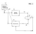
- FIG. 2a block diagram illustrating use of one or more example embodiments of the present invention in connection with a chemical mechanical polishing (“CMP”) process.
- CMPchemical mechanical polishing
- CVDchemical vapor deposition
- the present inventionmay also be used with types of process control systems, in addition to the semiconductor industry, which are concerned with measurement of true error (i.e., error not including white noise) as discriminated from observed error.
- the process control system 215controls the conventional controls of pressure, state, time, flow rate, etc., in connection with the wafers that are to be polished.
- the polish processreceives the input wafers together with the parameters 213 describing the polish process.
- the estimatorreceives from the process control system, parameters 213 describing the target result for the CMP polish process, performs a white noise estimation using an auto-regressive, stochastic sequence, updates the model parameters, and outputs the predicted value 209 .
- the polish process block 201obtains, determines and outputs observed, actual measurements 207 of the wafers, after they have been polished.
- Block 203determines the error in the prediction 211 , which is then further input into the estimator block 205 , to be used as feedback in connection with the recursive parameter estimation, e.g., to avoid over-reacting to the noise which may be present in the observed, actual measurement.
- the noiseis approximately extracted by the estimator block 205 utilizing the auto-regressive stochastic sequence discussed above.
- the updated model parameters 217may be provided to the process control system 215 , e.g., for further use.
- the process block 301outputs the observed measurements obtained from the first processing device 109 , in order to ultimately be used for making feedforward adjustments to the second processing device 111 . Those outputs are utilized in determining the variance, or predicted error, at block 103 of the observed values from the predicted values.
- the predicted erroris then utilized to make adjustments to the second processing device 111 , after being adjusted for the white noise component via the estimator and update model parameters block 305 , preferably utilizing the autoregressive stochastic sequence discussed above.
- the second processing devicecompensates for deficiencies and variances caused by the first processing device, such that according to this example, the wafers produced from the second processing device are within the range of specified target thickness.
- the measurement of the productsis described as being taken in relation to a pre-determined specification.
- the measurementscould be taken in relation to a real-time calculation based on prior measurements.
- multiple specificationscould be provided.
- FIG. 4is a flow chart representing one or more embodiments of the present invention.
- the observed value for the product(or other measurement) is determined.
- the predicted valueis determined, including for example from a specification or from a prior measurement, possibly incorporating white noise estimation as indicated in FIG. 1 .
- the difference, or predicted error, between the observed value and the predicted valueis obtained.
- the white noise component of the observed erroris calculated, using the current and prior observed errors, in an auto-regressive, stochastic sequence.
- the systemmay adjust a control parameter 411 . (For example, a gas pressure or temperature of the production environment might be adjusted, based on the systematic component.)
- the systemgets the next product to be measured, or obtains the next measurement.
- the difference between the measurements of the product, such as a wafer, and the specification for that productis calculated.
- the process control systemmay also calculate a statistical variance between such measurements and the specification.
- the specificationcould be pre-determined or could be based on a real-time calculation, such as determined by prior measurements.
- the process control systemmay, in effect, calculate two components, as explained above.
- the first componentis indicative of that portion of the difference caused by random noise, random variance, and/or normal deviation.
- the second component determined by the systemis indicative of the difference or variation caused by a systematic error or systematic variance over two or more products. Both the first and second components are calculated from a statistical variance.
- the process control systemmay or may not attempt to control the process. For example, the process control system may adjust one or more control parameters that affect the process and that are relevant to the processing device, such as gas pressure, temperature, etc., thereby controlling the production environment. Hence, the process may be more tightly controlled, based upon the calculated second component of the differences or variance.
- This inventionis described in connection with the semiconductor manufacturing industry. It can be used with other industries as well, particularly those that utilize measurements in an attempt to control variance in a process control system.
- the inventionconcerns determining, preferably but not necessarily in real-time, how much variance in a process control system can or cannot be controlled. According to one or more embodiments, the present invention determines how much of the standard deviation can be reduced and controlled.
- the process control system used in connection with operation of one or more embodiments of the present inventionmay include a general purpose computer 501 as illustrated in FIG. 5 , or a specially programmed special purpose computer. It may also be implemented as a distributed computer system rather than a single computer; some of the distributed systems might included embedded systems. Further, the programming may be distributed among one or more processing devices 503 themselves or other parts of the process control system. Similarly, the processing could be controlled by a software program on one or more computer systems or processors, or could be partially or wholly implemented in hardware. Moreover, the process control system may communicate directly or indirectly with the relevant processing devices and/or components thereof, such as metrology tools 505 . As another alternative, the portion of the process control system that is relevant may be embedded in the processing device itself.
- Deviationhas been described herein as controlled above a certain threshold. In certain situations, it would be appropriate to consider deviation as controllable in an inverse manner. In other situations, deviation may have a range, above and below which control is possible.
- the inventioncould be used in connection with processes that are not part of a process control system, but that use multiple measurements and that are susceptible to white noise.
- processesthat are not part of a process control system, but that use multiple measurements and that are susceptible to white noise.
- One exampleis the financial industry, where fluctuations in values over time may be due to some uncontrollable influences, for which a dynamic and/or more precise threshold may be calculated and/or adjustments made.
- FIG. 6is an illustration of a computer 58 used for implementing the computer processing in accordance with a computer-implemented embodiment of the present invention.
- the procedures described abovemay be presented in terms of program procedures executed on, for example, a computer or network of computers.
- computer 58has a central processing unit (CPU) 68 having disk drives 69 , 70 .
- Disk drives 69 , 70are merely symbolic of a number of disk drives that might be accommodated by computer 58 . Typically, these might be one or more of the following: a floppy disk drive 69 , a hard disk drive (not shown), and a CD ROM or digital video disk, as indicated by the slot at 70 .
- the number and type of drivesvaries, typically with different computer configurations.
- Disk drives 69 , 70are, in fact, options, and for space considerations, may be omitted from the computer system used in conjunction with the processes described herein.
- Computer 58also has a display 71 upon which information may be displayed.
- the displayis optional for the computer used in conjunction with the system described herein.
- a keyboard 72 and/or a pointing device 73such as a mouse 73 , may be provided as input devices to interface with central processing unit 68 .
- keyboard 72may be supplemented or replaced with a scanner, card reader, or other data input device.
- the pointing device 73may be a mouse, touch pad control device, track ball device, or any other type of pointing device.
- FIG. 7illustrates a block diagram of the internal hardware of the computer of FIG. 6 .
- CPU 75is the central processing unit of the system, performing calculations and logic operations required to execute a program.
- Read only memory (ROM) 76 and random access memory (RAM) 77constitute the main memory of the computer.
- Disk controller 78interfaces one or more disk drives to the system bus 74 . These disk drives may be floppy disk drives such as 79 , or CD ROM or DVD (digital video/versatile disk) drives, as at 80 , or internal or external hard drives 81 . As previously indicated these various disk drives and disk controllers are optional devices.
- a display interface 82permits information from bus 74 to be displayed on the display 83 .
- the display 83is an optional accessory for a central or remote computer in the communication network, as are infrared receiver 88 and transmitter 89 . Communication with external devices occurs using communications port 84 .
- the computermay also include an interface 85 , which allows for data input through the keyboard 86 or pointing device, such as a mouse 87 .
- the process control systemmay incorporate a factory automation system with a general purpose computer, or a specially programmed special purpose computer. It may also be implemented to include a distributed computer system rather than as a single computer; some of the distributed system might include embedded systems. Further, the programming may be distributed among processing devices and metrology tools and/or other parts of the process control system. Similarly, the processing could be controlled by a software program on one or more computer systems or processors, or could be partially or wholly implemented in hardware. Moreover, the factory automation system may communicate directly or indirectly with the relevant metrology tool(s), processing device(s), and metrology system(s); or the metrology tool(s), processing device(s) and metrology system(s) may communicate directly or indirectly with each other and the factory automation system.
- the systemmay be implemented on a web based computer, e.g., via an interface to collect and/or analyze data from many sources. It may be connected over a network, e.g., the Internet, an Intranet, or even on a single computer system. Moreover, portions of the system may be distributed (or not) over one or more computers, and some functions may be distributed to other hardware, such as tools, and still remain within the scope of this invention.
- the usermay interact with the system via e.g., a personal computer or over PDA, e.g., the Internet, an intranet, etc. Either of these may be implemented as a distributed computer system rather than a single computer.
- a communications linkmay be a dedicated link, a modem over a POTS line, and/or any other method of communicating between computers and/or users.
- the processingcould be controlled by a software program on one or more computer systems or processors, or could even be partially or wholly implemented in hardware.
- User interfacesmay be developed in connection with an HTML display format. It is possible to utilize alternative technology for displaying information, obtaining user instructions and for providing user interfaces.
- the system used in connection with the inventionmay rely on the integration of various components including, as appropriate and/or if desired, hardware and software servers, database engines, and/or other process control components.
- the configurationmay be, alternatively, network-based and may, if desired, use the Internet as an interface with the user.
- the systemmay store collected information in a database.
- An appropriate databasemay be on a standard server, for example, a small SunTM SparcTM or other remote location.
- the informationmay, for example, optionally be stored on a platform that may, for example, be UNIX-based.
- the various databasesmaybe in, for example, a UNIX format, but other standard data formats may be used.
- the process control systemis illustrated as having a single computer, the system according to one or more embodiments of the invention is optionally suitably equipped with a multitude or combination of processors or storage devices.
- the computermay be replaced by, or combined with, any suitable processing system operative in accordance with the principles of embodiments of the present invention, including sophisticated calculators, hand held, laptop/notebook, mini, mainframe and super computers, one or more embedded processors, as well as processing system network combinations of the same.
- portions of the systemmay be provided in any appropriate electronic format, including, for example, provided over a communication line as electronic signals, provided on floppy disk, provided on CD Rom, provided on optical disk memory, etc.
- Any presently available or future developed computer software language and/or hardware componentscan be employed in such embodiments of the present invention.
- at least some of the functionality mentioned abovecould be implemented using Visual Basic, C, C++ or any assembly language appropriate in view of the processor being used. It could also be written in an interpretive environment such as Java and transported to multiple destinations to various users.
- the inventionmay include a process and/or steps. Where steps are indicated, they may be performed in any order, unless expressly and necessarily limited to a particular order. Steps that are not so limited may be performed in any order.
Landscapes
- Engineering & Computer Science (AREA)
- Health & Medical Sciences (AREA)
- Artificial Intelligence (AREA)
- Computer Vision & Pattern Recognition (AREA)
- Evolutionary Computation (AREA)
- Medical Informatics (AREA)
- Software Systems (AREA)
- Physics & Mathematics (AREA)
- General Physics & Mathematics (AREA)
- Automation & Control Theory (AREA)
- Testing Or Measuring Of Semiconductors Or The Like (AREA)
- Feedback Control In General (AREA)
Abstract
Description
This application is related to co-pending application entitled “Dynamic Offset and Feedback Threshold,” filed on even date herewith and incorporated by reference.
1. Field of the Invention
The present invention concerns computer-implemented and/or computer-enabled methods, systems, and mediums for enabling improved control of errors during process control. More specifically, one or more embodiments of the present invention relate to distinguishing a variance due to white noise from a statistical process variance measured during process control, particularly in connection with semiconductor manufacturing.
2. Description of the Related Art
Detecting and controlling errors during a manufacturing process is an important goal. This is particularly true in connection with the process of manufacturing semiconductors. During the manufacturing process, various measurements are made in order to detect and/or determine errors, e.g., to detect when an observed value differs significantly from an intended target result. When the difference is sufficient, the manufacturing process control system will attempt to control (e.g., compensate for) the error so as to continue to produce products (e.g., chips) that are within acceptable ranges or tolerances from the target result.
In general, it has been observed that semiconductor devices processed in connection with a semiconductor manufacturing process will inevitably include at least some error or some deviation from the intended target result or specification. In order to determine when it is desired to perform additional control in order to make an adjustment during processing, conventional systems utilize a threshold value as a trigger. Whenever the additional control is triggered and the adjustment is made, however, the result following the adjustment still will usually deviate from the intended target result. Further, there are tolerances within which a tighter adjustment of a control does not effectively cause the material to be processed closer to specification, since the control is simply not capable of a sufficiently fine adjustment.
Conventionally, control of an error is attempted when one or more preconditions assigned to a tolerance range for the target specification, are evaluated using a statistical approach and are satisfied. The conventional statistical approach employs a standard deviation. Nevertheless, even when the process control system uses standard deviation as the threshold value, there is always a lack of precision, or a tolerance range within which it is not truly possible to control more tightly.
A significant reason often preventing tolerance ranges from being controlled more tightly is that some portion of the measurement, including the amount of observed value which is determined to be error, may actually be due to “white noise”. White noise does not necessarily represent an “error”. White noise represents an uncontrollable (and typically temporary) fluctuation in measurement. One example of white noise in a semiconductor manufacturing system is a sudden and temporary disturbance in ambient temperature, which is neither measured nor controlled, but would result in a change in thickness of the product. When determining whether an error occurred and/or how much (and whether) to compensate for any difference from the desired target result and/or to control an error that may occur during the manufacturing process, white noise should be taken into account.
The true amount of white noise occurring during manufacturing processes is not easily determined. In order to accommodate or adjust for white noise, the semiconductor industry conventionally utilizes a statistical process variance, or standard deviation, determined at optimal conditions, as an estimation of white noise. Thus, statistical process variance that is used as a substitute for what would otherwise be a truer (e.g., more real world) measurement of a general type of white noise is measured while the process, material to be processed, and processing device conditions are at an atypically pristine state. This type of measurement of white noise at pristine conditions yields a measurement during a best looking steady state performance, reflecting what cannot be controlled even at the best of conditions. The measurement at these atypical conditions is then utilized as an estimation of the white noise occurring throughout the manufacturing process under consideration.
The problem with the aforementioned conventional use of measurements at pristine conditions as a white noise estimate, despite its industry acceptance, is that it is not a reasonably accurate reflection of white noise that occurs during real manufacturing conditions. One of many reasons that measurements at pristine conditions do not reasonably reflect true conditions is that materials such as wafers processed in most front and back end processing devices in the semiconductor industry have relationships with or effects on subsequently processed wafers. Accordingly, for example, conditions applied to wafers that were previously processed in a processing device will have residual effects on wafers that are currently being processed in that processing device. An estimation of white noise derived from measurements taken while the processing device is at a steady state, consequently, does not reflect the fluctuations introduced during real-world run-to-run processing.
Regarding the aforementioned conventional techniques, statistical use of standard deviation in connection with observed deviation is illustrated, for example in “Statistical feedback control of a plasma etch process”, P. Mozumder et al., IEEE Transactions on Semiconductor Manufacturing, Vol. 7, No. 1 (February 1994) (incorporated herein by reference). The statistical variance Skat the kth run is calculated using the standard deviation as:
where
n=number of samples
X=deviation of observed value from predicted value
As can be seen, the standard deviation calculation does not distinguish between systematic variation and white noise variation components of the error. Hence, conventionally both the systematic and white noise variations are controlled together, rather than separately.
The conventional process control system thus compares this observed “combined” standard deviation to a threshold in order to determine if the deviation is unacceptable. Once the standard deviation greater than the threshold is detected, a tuning procedure in the process model is invoked in order to appropriately control the deviation. In essence, standard deviation-based methods only act to control when the standard deviation range is outside a particular threshold or trigger. In the conventional process control method, the standard deviation is used to determine the level for the threshold or trigger. Within the threshold, it is assumed that the deviation cannot be sufficiently controlled.
Therefore, there remains a need to have improved control, particularly within a tolerance range associated with a target specification. There also remains a need to address the effects of run-to-run conditions on such measurements.
The present invention provides a way to determine the “error” within standard deviation which is caused by two components: a white noise component and a systematic component. The white noise component is random noise and therefore is relatively non-controllable. The systematic component, in contrast, may be controlled by changing the control parameters. A ratio between the two components is calculated autoregressively. Based on the ratio and using the observed or measured error (as, e.g., typically made over the course of several measurements), the actual value of the error caused by the systematic component is calculated utilizing an autoregressive stochastic sequence. The actual value of this error is then used in determining how to change the control parameters. The autoregressive stochastic sequence addresses the issue of real-time control of the effects of run-to-run deviations, and provides a mechanism that can extract the white noise component from the statistical process variance in real time. This results in an ability to provide tighter control of feedback and feedforward variations and according to one or more embodiments of the present inventions, may be used in conjunction with a dynamic adaptation of estimated gain, estimation of recursive parameters, and dynamic filtration in searching for individual optimum vectors for example.
One potential use of one or more embodiments of the present invention is to provide an estimated gain adjustment which provides optimal weight factors via an autoregressive stochastic sequence.
In accordance with one or more embodiments of the invention, there is provided a computer-implemented method, system and/or a computer program product, for compensating for a variance between a measured characteristic of at least one product produced by a process and a target result of the characteristic, by differentiating a white noise component of the variance from a systematic component of the variance. An observed value is received for at least one product, and a target value is received for the product. A variance is determined between the observed value of at least one product and the target value of the at least one product. A first portion of the variance caused by white noise is determined. A second portion of the variance caused by a systematic component is determined. The first portion and/or second portions are used to adjust the process.
According to one or more embodiments of the invention, the products are semiconductor wafers, and the manufacturing process is an automated semiconductor manufacturing process.
According to one or more embodiments of the invention, the target value is derived from a specification, the specification being selected from at least one of a predetermined specification, and a real-time calculation taken from a plurality of prior observed values of products.
According to one or more embodiments of the invention, the process has at least one control parameter capable of being controlled; and the at least one control parameter is controlled during a process based on the second portion of the variance.
According to one or more embodiments of the invention, the value for each product of the plurality of products including the at least one product is determined; at least the second portion of the variance for the plurality of products is determined and the second portion of the variance is utilized as a threshold; and it is determined whether or not to perform the controlling step for the plurality of products when the observed value is outside the threshold.
According to one or more embodiments of the invention, the process includes at least one device on which the plurality of products including the at least one product is processed, the observed value being relative to the at least one device, the at least one device including the at least one control parameter; and controlling the at least one control parameter includes affecting the at least one device.
According to one or more embodiments of the invention, the process includes a plurality of devices including a first device and a second device on which the plurality of products including the at least one product are processed, the observed value being relative to the first device, the second device including the at least one control parameter; and controlling the at least one control parameter includes affecting at least the second device.
According to one or more embodiments of the present invention, the first portion and second portion are determined over two or more products.
According to one or more embodiments of the invention, the first portion and second portion of the variance are calculated using an autoregressive stochastic sequence.
According to one or more embodiments of the invention, the first portion and second portion of the variance are determined by:
δx=y/(1+z)
δx=y/(1+z)
- where
- δx=a value representing the variation that a system can control
- δw=a value representing the random variation that is not controlled
- where
According to one or more embodiments of the invention, the white noise includes at least one of random variance normal deviation, and an ambient fluctuation. Further, according to one or more embodiments of the invention, the first portion and second portion of the variance are calculated using an autoregressive stochastic sequence.
The above mentioned and other features and advantages of the present invention will become more readily apparent from the following detailed description and the accompanying drawings, in which:
The following detailed description includes many specific details. The inclusion of such details is for the purpose of illustration only and should not be understood to limit the invention. Throughout this discussion, similar elements are referred to by similar numbers in the various figures for ease of reference. In addition, features in one embodiment may be combined with features in other embodiments of the invention.
Differentiating the uncontrollable white noise component generated by a processing device from the systematic component, such as controllable errors generated or experienced by the device, assists in identifying an area in which additional control and/or more precise control may be applied within a process control system.
As contemplated by one or more embodiments of the present invention, the value of the white noise component may be extracted from the statistical process variance, such as by utilizing an autoregressive stochastic sequence (such as the one described below). This permits tighter control, which according to one or more embodiments of the present invention is helpful in determining a dynamic threshold for tighter feedback and/or feed forward control, while taking into consideration the real time run-to-run conditions relating to the process, material, and/or processing device.
An nthorder autoregressive stochastic sequence may be expressed as:
Xk=ρ1*Xk−1+ρ2*Xk−2+ . . . +ρn*Xk−n+Wk (2)
Xk=ρ1*Xk−1+ρ2*Xk−2+ . . . +ρn*Xk−n+Wk (2)
- where
- Wk=white noise
- ρn=auto-correlation coefficient at lag n
- Xk=deviation of observed value from predicted value at run k
- where
For the run-to-run control of the wafers:
Xk=ρ1*Xk−1+Wk (3)
Xk=ρ1*Xk−1+Wk (3)
To extract the white noise component, the variance analysis may be taken in two steps according to one or more embodiments of the invention. First,
Vx=ρ12*Vx+Vw (4)
Vx=ρ12*Vx+Vw (4)
- where
- Vx=variance of the signal
- Vw=variance of the white noise
- w=white noise
- x=signal
- where
Next,
δw/δx=(1−ρ12)0.5 (5)
δw/δx=(1−ρ12)0.5 (5)
- where δ=standard deviation.
Equation (5) provides an estimated gain adjustment, which is intended in effect to provide optimal weight factors taking into consideration a persistence of error conditions which may affect current conditions. The adjustment has cascaded functions of the above-described autoregressive stochastic sequence of equation (2).
From the above, it can be observed that:
Current parameter=previous parameter estimate+estimated gain*prediction error (6)
Current parameter=previous parameter estimate+estimated gain*prediction error (6)
Equations (7), (8) and (9) provide the estimated gain, weight factor and standard deviation derived from samples of the previous wafers.
Estimated Gain weight factor*Gain (7)
Weight factor=f(ρ1,δn) (8)
Estimated Gain weight factor*Gain (7)
Weight factor=f(ρ1,δn) (8)
- where δ=standard deviation from N samples of previous wafers
δN=δx+δw (9)
- where δ=standard deviation from N samples of previous wafers
From equation (5), the following can be derived:
δN=y (10)
δN=y (10)
- where y=calculated value from N samples of the previous wafers and
δw/δx=z (11) - where z=calculated value from equation (5)
- where y=calculated value from N samples of the previous wafers and
From equations (9), (10) and (11), it follows that:
δx=y/(1+z) (12)
δx=y/(1+z) (12)
- where
- δx=a value representing the variation that a system can control (i.e., the systematic component)
- δw=a value representing the random variation that is relatively non-controllable (i.e., the white noise component)
- where
Wafers that have been processed in a sequence (run-to-run) by a given device or system typically have a relationship to each other in terms of a variance that they create. In summary, equation (3) is one example of taking into consideration the run-to-run control of wafers; it addresses information representative of the sequence and the relationship between the wafers and the sequence. Equation (4) follows from equations (2) and (3). Equation (5) concerns the ratio between the white noise component and the observed value. Based on the ratio between the white noise component and the observed value, it can be determined what the total amount of error is. By utilizing feed forward analysis, the process in which the error is observed can be appropriately controlled. Estimated gain factors are utilized, as shown in equations (7) and (8). Referring to equation (9), the observed value now has been differentiated into two components, one of which is the white noise component and the other of which is real deviation, also referred to as the systematic component. Equations (10) and (11) follow from the foregoing.
Consider for instance that a CMP processing device will be used in a semiconductor process control system to polish twenty-five wafers. Xkis wafer twenty-four, Xk−1 is wafer twenty-three, etc. Because of the relationship and effect run-to-run wafers have on each other, the analysis used herein refers back to the previous wafer(s) (i.e., Xk−1, etc.) in determining how much control effectively may be applied to Xk, the wafer presently being processed.
Referring toFIG. 1 , the measured values (or raw data from which these values can be generated)107 for samples are obtained from, e.g., aprocessing device 106 and used byblock 101 to determine an observed value and by the white noise estimator and updatemodel parameter block 105. Theestimator block 105 performs a white noise estimation, using, for example, the aforementioned auto-regressive stochastic sequence.Estimator block 105 then updates the model parameters (taking the white noise component into account), and produces the predictedvalue 108 as output, that is, what the measured value is expected to be. In contrast, the process block101 merely produces an output indicative of the actual measuredvalue 111. Atblock 103, the positive or negative difference between the predictedoutput 108 and theactual output 111 is determined. This difference is utilized as the predictederror 113, which is then input back into theestimator block 105 to be used as feedback in connection with the recursive parameter estimation. Theestimator block 105 then utilizes the difference in the auto-regressive stochastic sequence (Such as equation (2)) to update the model. The updatedmodel parameters 115 are provided to theprocessing device 106, e.g., a CMP processing device, a CVD device, an etch device, etc.
According to one or more embodiments of the present invention, the white noise component is differentiated on a real time basis from systematic errors that occur during a manufacturing process. Alternatively, according to other embodiments, the differentiation is performed, but not on a real-time basis. The ability to differentiate the white noise component from the systematic component during real-time may be particularly useful within any number of industries (such as the semiconductor industry) in connection with obtaining higher quality, increased throughput, lower cost of operation, and shorter ramp-up time. Further, one or more embodiments of the present invention may provide more accurate determinations of error and may lead to improved test and yield analysis. One or more embodiments of the present invention are suitable for use in process control systems concerned with, for example, wafer-to-wafer thickness control, uniformity control, within-wafer range control, defect analysis and/or control, etch critical dimension control, chemical vapor deposition thickness and/or uniformity control, physical vapor deposition uniformity and/or thickness control, metrology variations, and other process control, analysis, and/or measurement situations and processing devices.
The following Table 1 illustrates simulated data comparing the calculation of a threshold using standard deviation to the calculation of a threshold with an embodiment of the present invention. In Table 1, the number of minimum samples is N=10.
| TABLE 1 | |||||
| Threshold | Threshold | ||||
| Sample | Simulated | with | with the | ||
| Number | Sample Value | Invention | |||
| 1 | 3927 | ||||
| 2 | 3893 | ||||
| 3 | 3797 | ||||
| 4 | 3713 | ||||
| 5 | 3627 | ||||
| 6 | 3602 | ||||
| 7 | 3694 | ||||
| 8 | 3732 | ||||
| 9 | 3753 | ||||
| 10 | 3781 | 45.0 | 14.1 | ||
| 11 | 3739 | 45.0 | 12.3 | ||
| 12 | 3694 | 45.0 | 9.2 | ||
| 13 | 3684 | 45.0 | 7.8 | ||
| 14 | 3673 | 45.0 | 7.8 | ||
| 15 | 3743 | 45.0 | 7.9 | ||
| 16 | 3753 | 45.0 | 5.4 | ||
| 17 | 3746 | 45.0 | 5.1 | ||
| 18 | 3710 | 45.0 | 5.3 | ||
| 19 | 3736 | 45.0 | 5.3 | ||
As shown in the above example simulated data, the threshold in a conventional process control system utilizing a threshold calculated using standard deviation is calculated to be at 45.0. In other words, the conventional standard deviation approach utilizes a fixed threshold or trigger. Where the observed values are within the threshold, the process control system does not attempt to control the error, whereas if the values are outside the threshold, the process control system does attempt to control the error. In contrast, the threshold calculated utilizing the invention is dynamic and varies, thereby presenting a sensitive threshold in real-time for feedback and feedforward control. The threshold varies from 14.1 down to 5.1 in the simulated data in Table 1. Hence, the present invention offers a more sensitive detection and/or control of “true” errors than the conventional process control system utilizing a fixed threshold.
Values within the threshold can be neglected since they cannot be effectively controlled. On the other hand, outside the threshold it is possible and useful to control the deviation. The reason that one ignores the value below the threshold is that this represents the calculated white noise component, which is not controllable. Once the threshold has been defined more accurately, as with the present invention, better control can be provided.
Reference is now made toFIG. 2 , a block diagram illustrating use of one or more example embodiments of the present invention in connection with a chemical mechanical polishing (“CMP”) process. However, it is not intended to limit the invention to CMP, as it can be applied in connection with a number of processes, such as chemical vapor deposition (“CVD”), or etching or many other processes within the semiconductor industry. Moreover, the present invention may also be used with types of process control systems, in addition to the semiconductor industry, which are concerned with measurement of true error (i.e., error not including white noise) as discriminated from observed error.
In the CMP process example ofFIG. 2 , theprocess control system 215 controls the conventional controls of pressure, state, time, flow rate, etc., in connection with the wafers that are to be polished. Atblock 201, the polish process receives the input wafers together with theparameters 213 describing the polish process. Atblock 205, the estimator receives from the process control system,parameters 213 describing the target result for the CMP polish process, performs a white noise estimation using an auto-regressive, stochastic sequence, updates the model parameters, and outputs the predictedvalue 209. The polish process block201 obtains, determines and outputs observed,actual measurements 207 of the wafers, after they have been polished. The difference between the actual measurements and the predicted value from theestimator block 205 is determined inblock 203.Block 203 determines the error in theprediction 211, which is then further input into theestimator block 205, to be used as feedback in connection with the recursive parameter estimation, e.g., to avoid over-reacting to the noise which may be present in the observed, actual measurement. According to one or more embodiments of the invention, the noise is approximately extracted by theestimator block 205 utilizing the auto-regressive stochastic sequence discussed above. The updated model parameters217 may be provided to theprocess control system 215, e.g., for further use.
As an example of another use of one or more embodiments of the present invention, consider that a specification is provided which requires the process control system to produce wafers of a certain thickness, among other things, so that a target thickness is achieved. In this particular processing sequence example, shown inFIG. 3 , twoprocessing devices FIG. 3 , the process block301 outputs the observed measurements obtained from thefirst processing device 109, in order to ultimately be used for making feedforward adjustments to thesecond processing device 111. Those outputs are utilized in determining the variance, or predicted error, atblock 103 of the observed values from the predicted values. The predicted error is then utilized to make adjustments to thesecond processing device 111, after being adjusted for the white noise component via the estimator and update model parameters block305, preferably utilizing the autoregressive stochastic sequence discussed above. By so doing, the second processing device compensates for deficiencies and variances caused by the first processing device, such that according to this example, the wafers produced from the second processing device are within the range of specified target thickness.
In the above description, the measurement of the products is described as being taken in relation to a pre-determined specification. Alternatively, according to one or more embodiments, the measurements could be taken in relation to a real-time calculation based on prior measurements. In accordance with at least one or more embodiments, multiple specifications could be provided.
Also, as described above, the difference between the measurements of the product, such as a wafer, and the specification for that product is calculated. However, the process control system may also calculate a statistical variance between such measurements and the specification. As described above, the specification could be pre-determined or could be based on a real-time calculation, such as determined by prior measurements.
From the difference or variance between observed values and predicted values, the process control system may, in effect, calculate two components, as explained above. The first component is indicative of that portion of the difference caused by random noise, random variance, and/or normal deviation. The second component determined by the system is indicative of the difference or variation caused by a systematic error or systematic variance over two or more products. Both the first and second components are calculated from a statistical variance.
If the actual variance exceeds a threshold, the process control system then may or may not attempt to control the process. For example, the process control system may adjust one or more control parameters that affect the process and that are relevant to the processing device, such as gas pressure, temperature, etc., thereby controlling the production environment. Hence, the process may be more tightly controlled, based upon the calculated second component of the differences or variance.
Other parameters that can be controlled in connection with semiconductor manufacturing include applying or changing electrical power, placing different gases into a chamber, changing distances between electrodes, etc. There are numerous variables in semi-conductor manufacturing that are to be measured and variances that may be controlled. The present invention is suitable for use in these situations.
This invention is described in connection with the semiconductor manufacturing industry. It can be used with other industries as well, particularly those that utilize measurements in an attempt to control variance in a process control system. The invention concerns determining, preferably but not necessarily in real-time, how much variance in a process control system can or cannot be controlled. According to one or more embodiments, the present invention determines how much of the standard deviation can be reduced and controlled.
The process control system used in connection with operation of one or more embodiments of the present invention may include ageneral purpose computer 501 as illustrated inFIG. 5 , or a specially programmed special purpose computer. It may also be implemented as a distributed computer system rather than a single computer; some of the distributed systems might included embedded systems. Further, the programming may be distributed among one ormore processing devices 503 themselves or other parts of the process control system. Similarly, the processing could be controlled by a software program on one or more computer systems or processors, or could be partially or wholly implemented in hardware. Moreover, the process control system may communicate directly or indirectly with the relevant processing devices and/or components thereof, such asmetrology tools 505. As another alternative, the portion of the process control system that is relevant may be embedded in the processing device itself.
Deviation has been described herein as controlled above a certain threshold. In certain situations, it would be appropriate to consider deviation as controllable in an inverse manner. In other situations, deviation may have a range, above and below which control is possible.
Furthermore, it is possible that the invention could be used in connection with processes that are not part of a process control system, but that use multiple measurements and that are susceptible to white noise. One example is the financial industry, where fluctuations in values over time may be due to some uncontrollable influences, for which a dynamic and/or more precise threshold may be calculated and/or adjustments made.
Viewed externally inFIG. 6 ,computer 58 has a central processing unit (CPU)68 havingdisk drives computer 58. Typically, these might be one or more of the following: afloppy disk drive 69, a hard disk drive (not shown), and a CD ROM or digital video disk, as indicated by the slot at70. The number and type of drives varies, typically with different computer configurations. Disk drives69,70 are, in fact, options, and for space considerations, may be omitted from the computer system used in conjunction with the processes described herein.
Adisplay interface 82 permits information frombus 74 to be displayed on thedisplay 83. Again, as indicated, thedisplay 83 is an optional accessory for a central or remote computer in the communication network, as are infrared receiver88 andtransmitter 89. Communication with external devices occurs usingcommunications port 84.
In addition to the standard components of the computer, the computer may also include aninterface 85, which allows for data input through thekeyboard 86 or pointing device, such as amouse 87.
As an example, the process control system may incorporate a factory automation system with a general purpose computer, or a specially programmed special purpose computer. It may also be implemented to include a distributed computer system rather than as a single computer; some of the distributed system might include embedded systems. Further, the programming may be distributed among processing devices and metrology tools and/or other parts of the process control system. Similarly, the processing could be controlled by a software program on one or more computer systems or processors, or could be partially or wholly implemented in hardware. Moreover, the factory automation system may communicate directly or indirectly with the relevant metrology tool(s), processing device(s), and metrology system(s); or the metrology tool(s), processing device(s) and metrology system(s) may communicate directly or indirectly with each other and the factory automation system.
As another example, the system may be implemented on a web based computer, e.g., via an interface to collect and/or analyze data from many sources. It may be connected over a network, e.g., the Internet, an Intranet, or even on a single computer system. Moreover, portions of the system may be distributed (or not) over one or more computers, and some functions may be distributed to other hardware, such as tools, and still remain within the scope of this invention. The user may interact with the system via e.g., a personal computer or over PDA, e.g., the Internet, an intranet, etc. Either of these may be implemented as a distributed computer system rather than a single computer. Similarly, a communications link may be a dedicated link, a modem over a POTS line, and/or any other method of communicating between computers and/or users. Moreover, the processing could be controlled by a software program on one or more computer systems or processors, or could even be partially or wholly implemented in hardware.
User interfaces may be developed in connection with an HTML display format. It is possible to utilize alternative technology for displaying information, obtaining user instructions and for providing user interfaces.
The invention has been discussed in connection with particular examples. However, the principles apply equally to other examples and/or realizations. For example, particular semi-conductor processes such as chemical vapor deposition were discussed, although the invention may be performed in connection with other semi-conductor processes. In addition, one or more embodiments of the invention are useful with systems not related to semi-conductor, in which processing adjustments are made and processing may benefit from distinguishing white noise. Such systems include, by way of example, systems for producing optical lenses, systems for controlling room temperature, and/or systems for controlling water temperature.
The system used in connection with the invention may rely on the integration of various components including, as appropriate and/or if desired, hardware and software servers, database engines, and/or other process control components. The configuration may be, alternatively, network-based and may, if desired, use the Internet as an interface with the user.
The system according to one or more embodiments of the invention may store collected information in a database. An appropriate database may be on a standard server, for example, a small Sun™ Sparc™ or other remote location. The information may, for example, optionally be stored on a platform that may, for example, be UNIX-based. The various databases maybe in, for example, a UNIX format, but other standard data formats may be used.
Although the process control system is illustrated as having a single computer, the system according to one or more embodiments of the invention is optionally suitably equipped with a multitude or combination of processors or storage devices. For example, the computer may be replaced by, or combined with, any suitable processing system operative in accordance with the principles of embodiments of the present invention, including sophisticated calculators, hand held, laptop/notebook, mini, mainframe and super computers, one or more embedded processors, as well as processing system network combinations of the same. Further, portions of the system may be provided in any appropriate electronic format, including, for example, provided over a communication line as electronic signals, provided on floppy disk, provided on CD Rom, provided on optical disk memory, etc.
Any presently available or future developed computer software language and/or hardware components can be employed in such embodiments of the present invention. For example, at least some of the functionality mentioned above could be implemented using Visual Basic, C, C++ or any assembly language appropriate in view of the processor being used. It could also be written in an interpretive environment such as Java and transported to multiple destinations to various users.
The invention may include a process and/or steps. Where steps are indicated, they may be performed in any order, unless expressly and necessarily limited to a particular order. Steps that are not so limited may be performed in any order.
While this invention has been described in conjunction with the specific embodiments outlined above, many alternatives, modifications and variations will be apparent to those skilled in the art. Accordingly, the preferred embodiments of the invention as set forth are intended to be illustrative and not limiting. Various changes may be made without departing from the spirit and scope of the invention as defined in the application. The foregoing detailed description includes many specific details. The inclusion of such detail is for the purpose of illustration only and should not be understood to limit the invention. In addition, features in one embodiment may be combined with features in other embodiments of the invention. Various changes may be made without departing from the scope of the invention as defined in the application.
Claims (34)
1. A system, implemented on at least one computer, for compensating for a variance between a measured characteristic of at least one product produced by a process and a target result of the characteristic, the system comprising:
(a) means for receiving an observed value for at least one product, and receiving a target value for the at least one product;
(b) means for determining a variance between the observed value of at least one product and the target value of the at least one product;
(c) means for determining a first portion of the variance caused by white noise;
(d) means for determining a second portion of the variance caused by a systematic component; and
(e) means, in the at least one computer, for using the determined first and/or second portions to adjust the process.
2. The system ofclaim 1 , wherein the at least one product is a semi-conductor wafer, and the process is an automated semiconductor manufacturing process.
3. The system ofclaim 1 , wherein the target value is derived from a specification, the specification being selected from at least one of a predetermined specification, and a real-time calculation taken from a plurality of prior observed values of products.
4. The system ofclaim 1 , wherein the process has at least one control parameter capable of being controlled, further comprising means for controlling the at least one control parameter during the process based on the second portion of the variance.
5. The system ofclaim 4 , further comprising means for determining the observed value for a plurality of products including the at least one product; determining at least the second portion of the variance for the plurality of products and utilizing the second portion of the variance for the plurality of products as a threshold; and determining whether or not to control the plurality of products when the observed value is outside the threshold.
6. The system ofclaim 4 , wherein the process includes at least one device on which the plurality of products including the at least one product is processed, the observed value being relative to the at least one device, the at least one device including the at least one control parameter, wherein controlling the at least one control parameter includes affecting the at least one device.
7. The system ofclaim 4 , wherein the process includes a plurality of devices including a first device and a second device on which the plurality of products including the at least one product are processed, the observed value being relative to the first device, the second device including the at least one control parameter, wherein controlling the at least one control parameter includes affecting at least the second device.
8. The system ofclaim 1 , wherein the first portion and second portion are determined over a plurality of products.
9. The system ofclaim 1 , wherein the first portion and second portion of the variance are calculated using an autoregressive stochastic sequence.
10. The system ofclaim 1 , wherein the first portion and second portion of the variance are substantially determined by:
δx=y/(1+z)
δx=y/(1+z)
where
δx=a value representing the variation that a system can control
y=calculated value from previous values
z=estimated gain adjustment.
11. The system ofclaim 1 , wherein the target value is derived from a specification, the specification being selected from at least one of a predetermined specification, and a real-time calculation taken from a plurality of prior observed values of products.
12. The system ofclaim 1 , wherein the white noise includes at least one of random variance, normal deviation, and an ambient fluctuation.
13. A computer-implemented method for compensating for a variance between a measured characteristic of at least one product produced by a process and a target result of the characteristic, comprising the steps of:
(a) receiving an observed value for at least one product, and receiving a target value for the at least one product;
(b) determining a variance between the observed value of at least one product and the target value of the at least one product;
(c) determining a first portion of the variance caused by white noise;
(d) determining a second portion of the variance caused by a systematic component; and
(e) using the determined first and/or second portions to adjust the process.
14. The method ofclaim 13 , wherein the at least one product is a semiconductor wafer, and the process is an automated semiconductor manufacturing process.
15. The method ofclaim 13 , wherein the target value is derived from a specification, the specification being selected from at least one of a predetermined specification, and a real-time calculation taken from a plurality of prior observed values of products.
16. The method ofclaim 13 , wherein the process has at least one control parameter capable of being controlled, further comprising the step of controlling the at least one control parameter during the process based on the second portion of the variance.
17. The method ofclaim 16 , further comprising the steps of determining the observed value for a plurality of products including the at least one product; determining at least the second portion of the variance for the plurality of products and utilizing the second portion of the variance for the plurality of products as a threshold; and determining whether or not to perform the controlling step for the plurality of products when the observed value is outside the threshold.
18. The method ofclaim 16 , wherein the process includes at least one device on which the plurality of products including the at least one product is processed, the observed value being relative to the at least one device, the at least one device including the at least one control parameter, wherein the step of controlling the at least one control parameter includes affecting the at least one device.
19. The method ofclaim 16 , wherein the process includes a plurality of devices including a first device and a second device on which the plurality of products including the at least one product are processed, the observed value being relative to the first device, the second device including the at least one control parameter, wherein the step of controlling the at least one control parameter includes affecting at least the second device.
20. The method ofclaim 3 , wherein the first portion and second portion are determined over a plurality of products.
21. The method ofclaim 13 , wherein the first portion and second portion of the variance are calculated using an autoregressive stochastic sequence.
22. The method ofclaim 13 , wherein the first portion and second portion of the variance are substantially determined by:
δx=y/(1+z)
δx=y/(1+z)
where
δx=a value representing the variation that a system can control
y=calculated value from previous values
z=estimated gain adjustment.
23. The method ofclaim 13 , wherein the white noise includes at least one of random variance, normal deviation, and an ambient fluctuation.
24. A computer program product for use in compensating for a variance between a measured characteristic of at least one product produced by a process and a target result of the characteristic by differentiating a white noise component of the variance from a systematic component of the variance, the computer program product comprising:
(a) at least one computer readable medium, readable by the manufacturing process;
(b) instructions, provided on the at least one computer readable medium, for receiving an observed value for at least one product, and receiving a target value for the at least one product;
(c) instructions, provided on the at least one computer readable medium, for determining a variance between the observed value of at least one product and the target value of the at least one product;
(d) instructions, provided on the at least one computer readable medium, for determining a first portion of the variance caused by white noise; and
(e) instructions, provided on the at least one computer readable medium, for determining a second portion of the variance caused by a systematic component; and
(f) instructions, provided on the at least one computer readable medium, for using the determined first and/or second portions to adjust the process.
25. The computer program product ofclaim 24 , wherein the at least one product includes a semi-conductor wafer, and the computer readable medium is readable by a process including an automated semiconductor manufacturing process.
26. The computer program product ofclaim 24 , wherein the target value is derived from a specification, the specification being selected from at least one of a predetermined specification, and a real-time calculation taken from a plurality of prior observed values of products.
27. The computer program product ofclaim 24 , wherein the process has at least one control parameter capable of being controlled, further comprising instructions, provided on the computer readable medium, for controlling the at least one control parameter during the process based on the second portion of the variance.
28. The computer program product ofclaim 27 , further comprising instructions, on the computer readable medium, for determining the observed value for the plurality of products including the at least one product; determining at least the second portion of the variance for the plurality of products and utilizing the second portion of the variance for the plurality of products as a threshold; and determining whether or not to execute the controlling instructions for the at least one product when the observed value is outside the threshold.
29. The computer program product ofclaim 28 , wherein the process includes at least one device on which the plurality of products including the at least one product is processed, the observed value being relative to the at least one device, the at least one device including the at least one control parameter, wherein the instructions for controlling the at least one control parameter includes affecting the at least one device.
30. The computer program product ofclaim 28 , wherein the process includes a plurality of devices including a first device and a second device on which the plurality of products including the at least one product are processed, the observed value being relative to the first device, the second device including the at least one control parameter, wherein the instructions for controlling the at least one control parameter includes affecting at least the second device.
31. The computer program product ofclaim 24 , wherein the first portion and the second portion are determined over a plurality of products.
32. The computer program product ofclaim 24 , wherein the first portion and second portion of the variance are calculated using an autoregressive stochastic sequence.
33. The computer program product ofclaim 24 , wherein the first portion and second portion of the variance are substantially determined by:
δx=y/(1+z)
δx=y/(1+z)
where
δx=a value representing the variation that a system can control
y=calculated value from previous values
z=estimated gain adjustment.
34. The computer program product ofclaim 24 , wherein the white noise includes at least one of random variance, normal deviation, and an ambient fluctuation.
Priority Applications (2)
| Application Number | Priority Date | Filing Date | Title |
|---|---|---|---|
| US10/856,016US7096085B2 (en) | 2004-05-28 | 2004-05-28 | Process control by distinguishing a white noise component of a process variance |
| US11/398,673US7221990B2 (en) | 2004-05-28 | 2006-04-06 | Process control by distinguishing a white noise component of a process variance |
Applications Claiming Priority (1)
| Application Number | Priority Date | Filing Date | Title |
|---|---|---|---|
| US10/856,016US7096085B2 (en) | 2004-05-28 | 2004-05-28 | Process control by distinguishing a white noise component of a process variance |
Related Child Applications (1)
| Application Number | Title | Priority Date | Filing Date |
|---|---|---|---|
| US11/398,673ContinuationUS7221990B2 (en) | 2004-05-28 | 2006-04-06 | Process control by distinguishing a white noise component of a process variance |
Publications (2)
| Publication Number | Publication Date |
|---|---|
| US20050278051A1 US20050278051A1 (en) | 2005-12-15 |
| US7096085B2true US7096085B2 (en) | 2006-08-22 |
Family
ID=35461546
Family Applications (2)
| Application Number | Title | Priority Date | Filing Date |
|---|---|---|---|
| US10/856,016Expired - Fee RelatedUS7096085B2 (en) | 2004-05-28 | 2004-05-28 | Process control by distinguishing a white noise component of a process variance |
| US11/398,673Expired - Fee RelatedUS7221990B2 (en) | 2004-05-28 | 2006-04-06 | Process control by distinguishing a white noise component of a process variance |
Family Applications After (1)
| Application Number | Title | Priority Date | Filing Date |
|---|---|---|---|
| US11/398,673Expired - Fee RelatedUS7221990B2 (en) | 2004-05-28 | 2006-04-06 | Process control by distinguishing a white noise component of a process variance |
Country Status (1)
| Country | Link |
|---|---|
| US (2) | US7096085B2 (en) |
Cited By (13)
| Publication number | Priority date | Publication date | Assignee | Title |
|---|---|---|---|---|
| US7349753B2 (en)* | 2004-05-28 | 2008-03-25 | Applied Materials, Inc. | Adjusting manufacturing process control parameter using updated process threshold derived from uncontrollable error |
| US20090138114A1 (en)* | 2005-05-11 | 2009-05-28 | Richard Gerard Burda | Method of release and product flow management for a manufacturing facility |
| US20090200674A1 (en)* | 2008-02-07 | 2009-08-13 | International Business Machines Corporation | Structure and method of forming transitional contacts between wide and thin beol wirings |
| US20090214760A1 (en)* | 2005-02-26 | 2009-08-27 | Leybold Optics Gmbh | Optical Monitoring System for Coating Processes |
| US7606681B2 (en) | 2006-11-03 | 2009-10-20 | Air Products And Chemicals, Inc. | System and method for process monitoring |
| US20110190921A1 (en)* | 2010-02-02 | 2011-08-04 | Applied Materials, Inc. | Flexible process condition monitoring |
| CN101813494B (en)* | 2010-02-25 | 2012-03-07 | 上海乐春重工机电设备有限公司 | Method for eliminating interference of sensor and outside thereof |
| US20130041482A1 (en)* | 2010-04-19 | 2013-02-14 | Abb Research Ltd | Method and system for updating a model in a model predictive controller |
| US8420531B2 (en) | 2011-06-21 | 2013-04-16 | International Business Machines Corporation | Enhanced diffusion barrier for interconnect structures |
| CN104020728A (en)* | 2013-03-01 | 2014-09-03 | 费希尔-罗斯蒙特系统公司 | Use of predictors in process control systems with wireless or intermittent process measurements |
| US9213322B1 (en)* | 2012-08-16 | 2015-12-15 | Western Digital (Fremont), Llc | Methods for providing run to run process control using a dynamic tuner |
| DE102007011248B4 (en)* | 2006-03-28 | 2016-05-19 | Infineon Technologies Ag | Process control system and method |
| US10916503B2 (en) | 2018-09-11 | 2021-02-09 | International Business Machines Corporation | Back end of line metallization structure |
Families Citing this family (10)
| Publication number | Priority date | Publication date | Assignee | Title |
|---|---|---|---|---|
| US7096085B2 (en)* | 2004-05-28 | 2006-08-22 | Applied Materials | Process control by distinguishing a white noise component of a process variance |
| US8014590B2 (en)* | 2005-12-07 | 2011-09-06 | Drvision Technologies Llc | Method of directed pattern enhancement for flexible recognition |
| JP2007294763A (en)* | 2006-04-26 | 2007-11-08 | Toshiba Corp | Semiconductor device manufacturing method and manufacturing system |
| US8036758B2 (en)* | 2008-04-07 | 2011-10-11 | Honeywell International Inc. | System and method for continuous supply chain control and optimization using stochastic calculus of variations approach |
| JP2010160787A (en)* | 2008-12-11 | 2010-07-22 | Jedat Inc | System for creating parameter information, system for estimating yields, program and recording medium |
| US8229588B2 (en)* | 2009-03-03 | 2012-07-24 | Taiwan Semiconductor Manufacturing Company, Ltd. | Method and system for tuning advanced process control parameters |
| TWI388954B (en)* | 2009-04-06 | 2013-03-11 | Inotera Memories Inc | Method for adjusting priority of lot of wafer |
| JP4737472B2 (en)* | 2009-10-26 | 2011-08-03 | シャープ株式会社 | Product manufacturing method and manufacturing system |
| CN104298268B (en)* | 2014-10-17 | 2017-01-25 | 北京七星华创电子股份有限公司 | Temperature control method of semiconductor technology equipment with feedforward compensation |
| CN115390451B (en)* | 2022-08-30 | 2025-07-22 | 联想(北京)有限公司 | Data processing method and device and electronic equipment |
Citations (409)
| Publication number | Priority date | Publication date | Assignee | Title |
|---|---|---|---|---|
| US3205485A (en) | 1960-10-21 | 1965-09-07 | Ti Group Services Ltd | Screening vane electro-mechanical transducer |
| US3229198A (en) | 1962-09-28 | 1966-01-11 | Hugo L Libby | Eddy current nondestructive testing device for measuring multiple parameter variables of a metal sample |
| US3767900A (en) | 1971-06-23 | 1973-10-23 | Cons Paper Inc | Adaptive controller having optimal filtering |
| US3920965A (en) | 1973-10-03 | 1975-11-18 | Siemens Ag | Method and apparatus for predictive control |
| US4000458A (en) | 1975-08-21 | 1976-12-28 | Bell Telephone Laboratories, Incorporated | Method for the noncontacting measurement of the electrical conductivity of a lamella |
| US4207520A (en) | 1978-04-06 | 1980-06-10 | The United States Of America As Represented By The Secretary Of The Air Force | Multiple frequency digital eddy current inspection system |
| US4209744A (en) | 1976-04-29 | 1980-06-24 | Fedosenko Jury K | Eddy current device for automatically testing the quality of elongated electrically conductive objects by non-destructive techniques |
| US4302721A (en) | 1978-05-08 | 1981-11-24 | Tencor Instruments | Non-contacting resistivity instrument with structurally related conductance and distance measuring transducers |
| US4368510A (en) | 1980-10-20 | 1983-01-11 | Leeds & Northrup Company | Automatic identification system for self tuning process controller |
| JPS6166104U (en) | 1984-10-03 | 1986-05-07 | ||
| JPS61171147A (en) | 1985-01-25 | 1986-08-01 | Fujitsu Ltd | How to check the coordinates of a wafer ham tup |
| US4609870A (en) | 1981-03-27 | 1986-09-02 | Hocking Electronics Limited | Lift off compensation of eddy current crack detection system by controlling damping resistance of oscillator |
| US4616308A (en) | 1983-11-15 | 1986-10-07 | Shell Oil Company | Dynamic process control |
| US4663703A (en) | 1985-10-02 | 1987-05-05 | Westinghouse Electric Corp. | Predictive model reference adaptive controller |
| US4698766A (en) | 1984-05-19 | 1987-10-06 | British Aerospace Plc | Industrial processing and manufacturing systems |
| US4750141A (en) | 1985-11-26 | 1988-06-07 | Ade Corporation | Method and apparatus for separating fixture-induced error from measured object characteristics and for compensating the measured object characteristic with the error, and a bow/warp station implementing same |
| US4755753A (en) | 1986-07-23 | 1988-07-05 | General Electric Company | Eddy current surface mapping system for flaw detection |
| US4757259A (en) | 1985-11-06 | 1988-07-12 | Cegedur Societe De Transformation De L'aluminium Pechiney | Method for measuring the thickness and temperature of a moving metal sheet by means of eddy currents |
| US4796194A (en) | 1986-08-20 | 1989-01-03 | Atherton Robert W | Real world modeling and control process |
| JPH01283934A (en) | 1988-05-11 | 1989-11-15 | Tokyo Electron Ltd | Etching apparatus |
| US4901218A (en) | 1987-08-12 | 1990-02-13 | Renishaw Controls Limited | Communications adaptor for automated factory system |
| US4938600A (en) | 1989-02-09 | 1990-07-03 | Interactive Video Systems, Inc. | Method and apparatus for measuring registration between layers of a semiconductor wafer |
| US4957605A (en) | 1989-04-17 | 1990-09-18 | Materials Research Corporation | Method and apparatus for sputter coating stepped wafers |
| US4967381A (en) | 1985-04-30 | 1990-10-30 | Prometrix Corporation | Process control interface system for managing measurement data |
| EP0397924A1 (en) | 1989-05-17 | 1990-11-22 | Koninklijke Philips Electronics N.V. | Work station controller module |
| JPH03202710A (en) | 1989-06-12 | 1991-09-04 | Tzn Forschungs & Entwicklungszentrum Unterluess Gmbh | Method and device for measuring layer thickness in non-contact state |
| US5089970A (en) | 1989-10-05 | 1992-02-18 | Combustion Engineering, Inc. | Integrated manufacturing system |
| CA2194855A1 (en) | 1990-08-31 | 1992-03-01 | Dennis A. Sierk | Process gas distribution system and method |
| US5108570A (en) | 1990-03-30 | 1992-04-28 | Applied Materials, Inc. | Multistep sputtering process for forming aluminum layer over stepped semiconductor wafer |
| US5208765A (en) | 1990-07-20 | 1993-05-04 | Advanced Micro Devices, Inc. | Computer-based method and system for product development |
| US5220517A (en) | 1990-08-31 | 1993-06-15 | Sci Systems, Inc. | Process gas distribution system and method with supervisory control |
| JPH05151231A (en) | 1990-08-14 | 1993-06-18 | Toshiba Corp | Manufacturing process management system |
| US5226118A (en) | 1991-01-29 | 1993-07-06 | Prometrix Corporation | Data analysis system and method for industrial process control systems |
| US5231585A (en) | 1989-06-22 | 1993-07-27 | Hitachi Ltd. | Computer-integrated manufacturing system and method |
| US5236868A (en) | 1990-04-20 | 1993-08-17 | Applied Materials, Inc. | Formation of titanium nitride on semiconductor wafer by reaction of titanium with nitrogen-bearing gas in an integrated processing system |
| JPH05216896A (en) | 1991-11-14 | 1993-08-27 | Toshiba Corp | Manufacturing process management system |
| US5240552A (en) | 1991-12-11 | 1993-08-31 | Micron Technology, Inc. | Chemical mechanical planarization (CMP) of a semiconductor wafer using acoustical waves for in-situ end point detection |
| JPH05266029A (en) | 1992-03-16 | 1993-10-15 | Toshiba Corp | Process flow preparing device |
| US5260868A (en) | 1986-08-11 | 1993-11-09 | Texas Instruments Incorporate | Method for calendaring future events in real-time |
| US5270222A (en) | 1990-12-31 | 1993-12-14 | Texas Instruments Incorporated | Method and apparatus for semiconductor device fabrication diagnosis and prognosis |
| US5283141A (en) | 1992-03-05 | 1994-02-01 | National Semiconductor | Photolithography control system and method using latent image measurements |
| US5295242A (en) | 1990-11-02 | 1994-03-15 | Consilium, Inc. | Apparatus and method for viewing relationships in a factory management system |
| JPH06110894A (en) | 1992-09-29 | 1994-04-22 | Toshiba Corp | Data verification system |
| US5309221A (en) | 1991-12-31 | 1994-05-03 | Corning Incorporated | Measurement of fiber diameters with high precision |
| JPH06176994A (en) | 1992-10-08 | 1994-06-24 | Toshiba Corp | Manufacturing rule check system |
| JPH06184434A (en) | 1992-12-16 | 1994-07-05 | Tonen Corp | Thermoplastic resin composition |
| JPH06252236A (en) | 1993-02-24 | 1994-09-09 | Toshiba Corp | Apparatus for checking and simulation of process flow |
| US5347446A (en) | 1991-02-08 | 1994-09-13 | Kabushiki Kaisha Toshiba | Model predictive control apparatus |
| JPH06260380A (en) | 1993-03-04 | 1994-09-16 | Toshiba Corp | Semiconductor production system |
| EP0621522A2 (en) | 1993-04-20 | 1994-10-26 | Praxair Inc. | Facility and gas management system |
| US5367624A (en) | 1993-06-11 | 1994-11-22 | Consilium, Inc. | Interface for controlling transactions in a manufacturing execution system |
| US5369544A (en) | 1993-04-05 | 1994-11-29 | Ford Motor Company | Silicon-on-insulator capacitive surface micromachined absolute pressure sensor |
| US5375064A (en) | 1993-12-02 | 1994-12-20 | Hughes Aircraft Company | Method and apparatus for moving a material removal tool with low tool accelerations |
| US5398336A (en) | 1990-10-16 | 1995-03-14 | Consilium, Inc. | Object-oriented architecture for factory floor management |
| US5402367A (en) | 1993-07-19 | 1995-03-28 | Texas Instruments, Incorporated | Apparatus and method for model based process control |
| US5408405A (en) | 1993-09-20 | 1995-04-18 | Texas Instruments Incorporated | Multi-variable statistical process controller for discrete manufacturing |
| US5410473A (en) | 1992-01-07 | 1995-04-25 | Fukuda Denshi Kabushiki Kaisha | Method and apparatus for recording electrocardiogram information |
| US5420796A (en) | 1993-12-23 | 1995-05-30 | Vlsi Technology, Inc. | Method of inspecting planarity of wafer surface after etchback step in integrated circuit fabrication |
| US5427878A (en) | 1991-06-26 | 1995-06-27 | Digital Equipment Corporation | Semiconductor wafer processing with across-wafer critical dimension monitoring using optical endpoint detection |
| US5444837A (en) | 1993-01-12 | 1995-08-22 | Sextant Avionique | Method for structuring information used in an industrial process and its application to aircraft piloting assistance |
| US5469361A (en) | 1991-08-08 | 1995-11-21 | The Board Of Regents Acting For And On Behalf Of The University Of Michigan | Generic cell controlling method and apparatus for computer integrated manufacturing system |
| WO1995034866A1 (en) | 1994-06-14 | 1995-12-21 | Telefonaktiebolaget Lm Ericsson | A method and system for manipulating intelligent representations of real equipment within a graphical computer system |
| US5485082A (en) | 1990-04-11 | 1996-01-16 | Micro-Epsilon Messtechnik Gmbh & Co. Kg | Method of calibrating a thickness measuring device and device for measuring or monitoring the thickness of layers, tapes, foils, and the like |
| US5490097A (en) | 1993-03-22 | 1996-02-06 | Fujitsu Limited | System and method for modeling, analyzing and executing work process plans |
| JPH0850161A (en) | 1994-08-05 | 1996-02-20 | Matsushita Electron Corp | Measuring method of semiconductor device |
| US5495417A (en) | 1990-08-14 | 1996-02-27 | Kabushiki Kaisha Toshiba | System for automatically producing different semiconductor products in different quantities through a plurality of processes along a production line |
| US5497381A (en) | 1993-10-15 | 1996-03-05 | Analog Devices, Inc. | Bitstream defect analysis method for integrated circuits |
| JPH0823166B2 (en) | 1993-04-05 | 1996-03-06 | 西武ポリマ化成株式会社 | Construction method of culvert joint |
| US5503707A (en) | 1993-09-22 | 1996-04-02 | Texas Instruments Incorporated | Method and apparatus for process endpoint prediction based on actual thickness measurements |
| US5511005A (en) | 1994-02-16 | 1996-04-23 | Ade Corporation | Wafer handling and processing system |
| US5519605A (en) | 1994-10-24 | 1996-05-21 | Olin Corporation | Model predictive control apparatus and method |
| JPH08149583A (en) | 1994-11-21 | 1996-06-07 | Mitsubishi Electric Corp | Process controller and data monitoring method |
| US5525808A (en) | 1992-01-23 | 1996-06-11 | Nikon Corporaton | Alignment method and alignment apparatus with a statistic calculation using a plurality of weighted coordinate positions |
| US5526293A (en) | 1993-12-17 | 1996-06-11 | Texas Instruments Inc. | System and method for controlling semiconductor wafer processing |
| US5534289A (en) | 1995-01-03 | 1996-07-09 | Competitive Technologies Inc. | Structural crack monitoring technique |
| US5541510A (en) | 1995-04-06 | 1996-07-30 | Kaman Instrumentation Corporation | Multi-Parameter eddy current measuring system with parameter compensation technical field |
| US5546312A (en) | 1993-09-20 | 1996-08-13 | Texas Instruments Incorporated | Use of spatial models for simultaneous control of various non-uniformity metrics |
| US5553195A (en) | 1993-09-30 | 1996-09-03 | U.S. Philips Corporation | Dynamic neural net |
| JPH08304023A (en) | 1995-04-28 | 1996-11-22 | Dainippon Screen Mfg Co Ltd | Measuring-point mapping device and measuring apparatus for semiconductor wafer utilizing the device |
| EP0747795A2 (en) | 1995-06-07 | 1996-12-11 | Xerox Corporation | A system for generically describing and scheduling operation of a modular printing machine |
| US5586039A (en) | 1993-03-29 | 1996-12-17 | Texas Instruments Incorporated | Computer-aided manufacturing support method and system for specifying relationships and dependencies between process type components |
| US5599423A (en) | 1995-06-30 | 1997-02-04 | Applied Materials, Inc. | Apparatus and method for simulating and optimizing a chemical mechanical polishing system |
| JPH0934535A (en) | 1995-07-13 | 1997-02-07 | Mitsubishi Electric Corp | Maintenance notification method |
| US5602492A (en) | 1992-03-13 | 1997-02-11 | The United States Of America As Represented By The Secretary Of Commerce | Electrical test structure and method for measuring the relative locations of conducting features on an insulating substrate |
| US5603707A (en) | 1995-11-28 | 1997-02-18 | The Procter & Gamble Company | Absorbent article having a rewet barrier |
| US5617023A (en) | 1995-02-02 | 1997-04-01 | Otis Elevator Company | Industrial contactless position sensor |
| US5627083A (en) | 1993-08-03 | 1997-05-06 | Nec Corporation | Method of fabricating semiconductor device including step of forming superposition error measuring patterns |
| US5629216A (en) | 1994-06-30 | 1997-05-13 | Seh America, Inc. | Method for producing semiconductor wafers with low light scattering anomalies |
| US5642296A (en) | 1993-07-29 | 1997-06-24 | Texas Instruments Incorporated | Method of diagnosing malfunctions in semiconductor manufacturing equipment |
| US5646870A (en) | 1995-02-13 | 1997-07-08 | Advanced Micro Devices, Inc. | Method for setting and adjusting process parameters to maintain acceptable critical dimensions across each die of mass-produced semiconductor wafers |
| US5649169A (en) | 1995-06-20 | 1997-07-15 | Advanced Micro Devices, Inc. | Method and system for declustering semiconductor defect data |
| US5654903A (en) | 1995-11-07 | 1997-08-05 | Lucent Technologies Inc. | Method and apparatus for real time monitoring of wafer attributes in a plasma etch process |
| US5655951A (en) | 1995-09-29 | 1997-08-12 | Micron Technology, Inc. | Method for selectively reconditioning a polishing pad used in chemical-mechanical planarization of semiconductor wafers |
| US5663797A (en) | 1996-05-16 | 1997-09-02 | Micron Technology, Inc. | Method and apparatus for detecting the endpoint in chemical-mechanical polishing of semiconductor wafers |
| US5665214A (en) | 1995-05-03 | 1997-09-09 | Sony Corporation | Automatic film deposition control method and system |
| US5666297A (en) | 1994-05-13 | 1997-09-09 | Aspen Technology, Inc. | Plant simulation and optimization software apparatus and method using dual execution models |
| US5664987A (en) | 1994-01-31 | 1997-09-09 | National Semiconductor Corporation | Methods and apparatus for control of polishing pad conditioning for wafer planarization |
| US5665199A (en) | 1995-06-23 | 1997-09-09 | Advanced Micro Devices, Inc. | Methodology for developing product-specific interlayer dielectric polish processes |
| US5667424A (en) | 1996-09-25 | 1997-09-16 | Chartered Semiconductor Manufacturing Pte Ltd. | New chemical mechanical planarization (CMP) end point detection apparatus |
| JPH09246547A (en) | 1996-03-11 | 1997-09-19 | Fujitsu Ltd | Semiconductor device and manufacturing method thereof |
| US5674787A (en) | 1996-01-16 | 1997-10-07 | Sematech, Inc. | Selective electroless copper deposited interconnect plugs for ULSI applications |
| US5695810A (en) | 1996-11-20 | 1997-12-09 | Cornell Research Foundation, Inc. | Use of cobalt tungsten phosphide as a barrier material for copper metallization |
| US5698989A (en) | 1994-10-06 | 1997-12-16 | Applied Materilas, Inc. | Film sheet resistance measurement |
| JPH1034522A (en) | 1996-07-17 | 1998-02-10 | Nikon Corp | Polishing apparatus for CMP and apparatus system for CMP |
| US5719796A (en) | 1995-12-04 | 1998-02-17 | Advanced Micro Devices, Inc. | System for monitoring and analyzing manufacturing processes using statistical simulation with single step feedback |
| WO1998005066A3 (en) | 1996-07-26 | 1998-03-05 | Speedfam Corp | Methods and apparatus for the in-process detection and measurement of thin film layers |
| US5735055A (en) | 1996-04-23 | 1998-04-07 | Aluminum Company Of America | Method and apparatus for measuring the thickness of an article at a plurality of points |
| US5740033A (en) | 1992-10-13 | 1998-04-14 | The Dow Chemical Company | Model predictive controller |
| US5740429A (en) | 1995-07-07 | 1998-04-14 | Advanced Micro Devices, Inc. | E10 reporting tool |
| US5751582A (en) | 1995-09-25 | 1998-05-12 | Texas Instruments Incorporated | Controlling process modules using site models and monitor wafer control |
| US5754297A (en) | 1994-01-28 | 1998-05-19 | Applied Materials, Inc. | Method and apparatus for monitoring the deposition rate of films during physical vapor deposition |
| US5761065A (en) | 1995-03-30 | 1998-06-02 | Advanced Micro Devices, Inc. | Arrangement and method for detecting sequential processing effects in manufacturing |
| US5761064A (en) | 1995-10-06 | 1998-06-02 | Advanced Micro Devices, Inc. | Defect management system for productivity and yield improvement |
| US5764543A (en) | 1995-06-16 | 1998-06-09 | I2 Technologies, Inc. | Extensible model network representation system for process planning |
| JPH10173029A (en) | 1996-12-13 | 1998-06-26 | Dainippon Screen Mfg Co Ltd | Method of determining measuring positions of wafer |
| US5777901A (en) | 1995-09-29 | 1998-07-07 | Advanced Micro Devices, Inc. | Method and system for automated die yield prediction in semiconductor manufacturing |
| US5787021A (en) | 1994-12-28 | 1998-07-28 | Detusche Itt Industries Gmbh | Information system for production control |
| US5787269A (en) | 1994-09-20 | 1998-07-28 | Ricoh Company, Ltd. | Process simulation apparatus and method for selecting an optimum simulation model for a semiconductor manufacturing process |
| US5808303A (en) | 1997-01-29 | 1998-09-15 | Art Aerospace Research Technologies Inc. | Infrared screening and inspection system |
| US5812407A (en) | 1996-08-13 | 1998-09-22 | Sony Corporation | Apparatus for correcting and holding front surface of sheet |
| EP0869652A2 (en) | 1997-04-01 | 1998-10-07 | Tumbleweed Software Corporation | Document delivery system |
| WO1998045090A1 (en) | 1997-04-04 | 1998-10-15 | Obsidian, Inc. | Polishing media magazine for improved polishing |
| US5824599A (en) | 1996-01-16 | 1998-10-20 | Cornell Research Foundation, Inc. | Protected encapsulation of catalytic layer for electroless copper interconnect |
| US5823854A (en) | 1996-05-28 | 1998-10-20 | Industrial Technology Research Institute | Chemical-mechanical polish (CMP) pad conditioner |
| US5825913A (en) | 1995-07-18 | 1998-10-20 | Cognex Corporation | System for finding the orientation of a wafer |
| US5825356A (en) | 1996-03-18 | 1998-10-20 | Wall Data Incorporated | Help system with semitransparent window for disabling controls |
| US5828778A (en) | 1995-07-13 | 1998-10-27 | Matsushita Electric Industrial Co., Ltd. | Method and apparatus for analyzing failure of semiconductor wafer |
| US5831851A (en) | 1995-03-21 | 1998-11-03 | Seagate Technology, Inc. | Apparatus and method for controlling high throughput sputtering |
| US5832224A (en) | 1988-09-14 | 1998-11-03 | Digital Equipment Corporation | Entity management system |
| EP0877308A2 (en) | 1997-05-06 | 1998-11-11 | Tokyo Electron Limited | Control apparatus and control method |
| US5838951A (en) | 1996-02-29 | 1998-11-17 | Anam Industrial Co., Ltd | Wafer map conversion method |
| US5844554A (en) | 1996-09-17 | 1998-12-01 | Bt Squared Technologies, Inc. | Methods and systems for user interfaces and constraint handling configurations software |
| EP0881040A2 (en) | 1997-05-28 | 1998-12-02 | LAM Research Corporation | Method and apparatus for in-situ monitoring of thickness using a multi-wavelength spectrometer during chemical-mechanical polishing |
| US5859975A (en) | 1993-12-15 | 1999-01-12 | Hewlett-Packard, Co. | Parallel processing computer system having shared coherent memory and interconnections utilizing separate undirectional request and response lines for direct communication or using crossbar switching device |
| US5859964A (en) | 1996-10-25 | 1999-01-12 | Advanced Micro Devices, Inc. | System and method for performing real time data acquisition, process modeling and fault detection of wafer fabrication processes |
| US5859777A (en) | 1996-05-14 | 1999-01-12 | Toshiba Kikai Kabushiki Kaisha | Casting control support system for die casting machines |
| US5857258A (en) | 1992-03-13 | 1999-01-12 | The United States Of America As Represented By The Secretary Of Commerce | Electrical test structure and method for measuring the relative locations of conductive features on an insulating substrate |
| US5862054A (en) | 1997-02-20 | 1999-01-19 | Taiwan Semiconductor Manufacturing Company, Ltd. | Process monitoring system for real time statistical process control |
| US5863807A (en) | 1995-09-20 | 1999-01-26 | Samsung Electronics Co., Ltd. | Manufacturing method of a semiconductor integrated circuit |
| US5867389A (en) | 1995-11-29 | 1999-02-02 | Dainippon Screen Mfg. Co., Ltd. | Substrate processing management system with recipe copying functions |
| EP0895145A1 (en) | 1997-08-01 | 1999-02-03 | Hewlett-Packard Company | Process control device |
| US5870306A (en) | 1996-06-13 | 1999-02-09 | Mitsubishi Denki Kabushiki Kaisha | Automatic programming method and device for multi-system machine tool |
| US5871805A (en) | 1996-04-08 | 1999-02-16 | Lemelson; Jerome | Computer controlled vapor deposition processes |
| WO1999009371A1 (en) | 1997-08-19 | 1999-02-25 | Micron Technology, Inc. | Method and apparatus for detecting the endpoint in chemical-mechanical polishing of semiconductor wafers |
| JPH1167853A (en) | 1997-08-26 | 1999-03-09 | Mitsubishi Electric Corp | Wafer map analysis auxiliary system and wafer map analysis method |
| US5883437A (en) | 1994-12-28 | 1999-03-16 | Hitachi, Ltd. | Method and apparatus for inspection and correction of wiring of electronic circuit and for manufacture thereof |
| US5889991A (en) | 1996-12-06 | 1999-03-30 | International Business Machines Corp. | Method and system for customizing a palette using any java class |
| EP0910123A1 (en) | 1996-03-19 | 1999-04-21 | Hitachi, Ltd. | Process control system |
| US5901313A (en) | 1991-03-01 | 1999-05-04 | Ast Research, Inc. | Application management system |
| US5903455A (en) | 1996-02-06 | 1999-05-11 | Fisher-Rosemount Systems, Inc. | Interface controls for use in a field device management system |
| JPH11126816A (en) | 1997-10-23 | 1999-05-11 | Dainippon Screen Mfg Co Ltd | Method for correcting and deciding coordinates of objective point on wafer |
| JPH11135601A (en) | 1997-10-29 | 1999-05-21 | Dainippon Screen Mfg Co Ltd | Method for creating measurement information and measurement position of wafer |
| WO1999025520A1 (en) | 1997-11-18 | 1999-05-27 | Speedfam-Ipec Corporation | Method and apparatus for modeling a chemical mechanical polishing process |
| US5910011A (en) | 1997-05-12 | 1999-06-08 | Applied Materials, Inc. | Method and apparatus for monitoring processes using multiple parameters of a semiconductor wafer processing system |
| US5912678A (en) | 1997-04-14 | 1999-06-15 | Texas Instruments Incorporated | Process flow design at the module effects level through the use of acceptability regions |
| US5916016A (en) | 1997-10-23 | 1999-06-29 | Vlsi Technology, Inc. | Methods and apparatus for polishing wafers |
| US5923553A (en) | 1995-12-21 | 1999-07-13 | Samsung Electronics Co., Ltd. | Method for controlling a semiconductor manufacturing process by failure analysis feedback |
| US5926690A (en) | 1997-05-28 | 1999-07-20 | Advanced Micro Devices, Inc. | Run-to-run control process for controlling critical dimensions |
| US5930138A (en) | 1995-08-22 | 1999-07-27 | Advanced Micro Devices, Inc. | Arrangement and method for detecting sequential processing effects in manufacturing using predetermined sequences within runs |
| EP0932195A1 (en) | 1997-12-30 | 1999-07-28 | International Business Machines Corporation | Method and system for semiconductor wafer fabrication process real-time in-situ supervision |
| EP0932194A1 (en) | 1997-12-30 | 1999-07-28 | International Business Machines Corporation | Method and system for semiconductor wafer fabrication process real-time in-situ interactive supervision |
| US5940300A (en) | 1996-12-12 | 1999-08-17 | Mitsubishi Denki Kabushiki Kaisha | Method and apparatus for analyzing a fabrication line |
| US5943550A (en) | 1996-03-29 | 1999-08-24 | Advanced Micro Devices, Inc. | Method of processing a semiconductor wafer for controlling drive current |
| US5943237A (en) | 1996-10-21 | 1999-08-24 | U.S. Philips Corporation | Method and system for assessing a measurement procedure and measurement-induced uncertainties on a batchwise manufacturing process of discrete products |
| US5960185A (en) | 1996-06-24 | 1999-09-28 | International Business Machines Corporation | Method and apparatus for wafer disposition based on systematic error modeling |
| US5963881A (en) | 1995-09-22 | 1999-10-05 | Texas Instruments Incorporated | Method and system for enhancing the identification of causes of variations in the performance of manufactured articles |
| US5961369A (en) | 1996-07-18 | 1999-10-05 | Speedfam-Ipec Corp. | Methods for the in-process detection of workpieces with a monochromatic light source |
| US5975994A (en) | 1997-06-11 | 1999-11-02 | Micron Technology, Inc. | Method and apparatus for selectively conditioning a polished pad used in planarizng substrates |
| US5978751A (en) | 1997-02-25 | 1999-11-02 | International Business Machines Corporation | Variegated manufacturing process test method and apparatus |
| US5982920A (en) | 1997-01-08 | 1999-11-09 | Lockheed Martin Energy Research Corp. Oak Ridge National Laboratory | Automated defect spatial signature analysis for semiconductor manufacturing process |
| WO1999059200A1 (en) | 1998-05-11 | 1999-11-18 | Applied Materials, Inc. | Fab yield enhancement system |
| US6002989A (en) | 1996-04-02 | 1999-12-14 | Hitachi, Ltd. | System for quality control where inspection frequency of inspection apparatus is reset to minimize expected total loss based on derived frequency function and loss value |
| US6012048A (en) | 1997-05-30 | 2000-01-04 | Capital Security Systems, Inc. | Automated banking system for dispensing money orders, wire transfer and bill payment |
| WO2000000874A1 (en) | 1998-06-26 | 2000-01-06 | Advanced Micro Devices, Inc. | System and method for controlling the manufacture of discrete parts in semiconductor fabrication using model predictive control |
| US6017771A (en) | 1998-04-27 | 2000-01-25 | Taiwan Semiconductor Manufacturing Company, Ltd. | Method and system for yield loss analysis by yield management system |
| WO2000005759A1 (en) | 1998-07-20 | 2000-02-03 | Isemicon, Inc | Method for measuring number of yield loss chips and number of poor chips by type due to defect of semiconductor chips |
| US6036349A (en) | 1995-07-27 | 2000-03-14 | Health Designs, Inc. | Method and apparatus for validation of model-based predictions |
| US6037664A (en) | 1997-08-20 | 2000-03-14 | Sematech Inc | Dual damascene interconnect structure using low dielectric constant material for an inter-level dielectric layer |
| US6041263A (en) | 1996-10-01 | 2000-03-21 | Aspen Technology, Inc. | Method and apparatus for simulating and optimizing a plant model |
| US6041270A (en) | 1997-12-05 | 2000-03-21 | Advanced Micro Devices, Inc. | Automatic recipe adjust and download based on process control window |
| US6054379A (en) | 1998-02-11 | 2000-04-25 | Applied Materials, Inc. | Method of depositing a low k dielectric with organo silane |
| US6059636A (en) | 1997-07-11 | 2000-05-09 | Tokyo Seimitsu Co., Ltd. | Wafer polishing apparatus |
| US6064759A (en) | 1996-11-08 | 2000-05-16 | Buckley; B. Shawn | Computer aided inspection machine |
| US6072313A (en) | 1995-04-10 | 2000-06-06 | International Business Machines Corporation | In-situ monitoring and control of conductive films by detecting changes in induced eddy currents |
| US6074443A (en) | 1996-10-21 | 2000-06-13 | Applied Materials, Inc. | Method and apparatus for scheduling wafer processing within a multiple chamber semiconductor wafer processing tool having a multiple blade robot |
| WO2000035063A1 (en) | 1998-12-07 | 2000-06-15 | Abb Power T & D Company Inc. | Architecture layer interfacing devices and applications |
| US6077412A (en) | 1997-08-22 | 2000-06-20 | Cutek Research, Inc. | Rotating anode for a wafer processing chamber |
| US6078845A (en) | 1996-11-25 | 2000-06-20 | Schlumberger Technologies, Inc. | Apparatus for carrying semiconductor devices |
| JP2000183001A (en) | 1998-12-10 | 2000-06-30 | Okamoto Machine Tool Works Ltd | Polish end-point detecting method for wafer and chemical-mechanical polishing device used for the same |
| US6094688A (en) | 1997-01-08 | 2000-07-25 | Crossworlds Software, Inc. | Modular application collaboration including filtering at the source and proxy execution of compensating transactions to conserve server resources |
| US6096649A (en) | 1999-10-25 | 2000-08-01 | Taiwan Semiconductor Manufacturing Company | Top metal and passivation procedures for copper damascene structures |
| US6097887A (en) | 1997-10-27 | 2000-08-01 | Kla-Tencor Corporation | Software system and method for graphically building customized recipe flowcharts |
| US6100195A (en) | 1998-12-28 | 2000-08-08 | Chartered Semiconductor Manu. Ltd. | Passivation of copper interconnect surfaces with a passivating metal layer |
| US6112130A (en) | 1996-10-02 | 2000-08-29 | Kabushiki Kaisha Toshiba | Semiconductor product manufacturing execution system and semiconductor product manufacturing method |
| US6114238A (en) | 1998-01-26 | 2000-09-05 | United Silicon Incorporated | Self-aligned metal nitride for copper passivation |
| US6113462A (en) | 1997-12-18 | 2000-09-05 | Advanced Micro Devices, Inc. | Feedback loop for selective conditioning of chemical mechanical polishing pad |
| WO2000054325A1 (en) | 1999-03-10 | 2000-09-14 | Nova Measuring Instruments Ltd. | Method and apparatus for monitoring a chemical mechanical planarization process applied to metal-based patterned objects |
| GB2347885A (en) | 1998-10-15 | 2000-09-20 | Nec Corp | Control of pad dresser in chemical-mechanical polishing appararus |
| US6127263A (en) | 1998-07-10 | 2000-10-03 | Applied Materials, Inc. | Misalignment tolerant techniques for dual damascene fabrication |
| US6128016A (en) | 1996-12-20 | 2000-10-03 | Nec Corporation | Graphic user interface for managing a server system |
| US6136163A (en) | 1999-03-05 | 2000-10-24 | Applied Materials, Inc. | Apparatus for electro-chemical deposition with thermal anneal chamber |
| US6141660A (en) | 1998-07-16 | 2000-10-31 | International Business Machines Corporation | Command line interface for creating business objects for accessing a hierarchical database |
| US6143646A (en) | 1997-06-03 | 2000-11-07 | Motorola Inc. | Dual in-laid integrated circuit structure with selectively positioned low-K dielectric isolation and method of formation |
| US6148099A (en) | 1997-07-03 | 2000-11-14 | Neopath, Inc. | Method and apparatus for incremental concurrent learning in automatic semiconductor wafer and liquid crystal display defect classification |
| US6148246A (en) | 1997-06-13 | 2000-11-14 | Canon Kabushiki Kaisha | Semiconductor process system, its control method, computer readable memory, and device manufacturing method |
| US6148239A (en) | 1997-12-12 | 2000-11-14 | Advanced Micro Devices, Inc. | Process control system using feed forward control threads based on material groups |
| US6150270A (en) | 1998-01-07 | 2000-11-21 | Kabushiki Kaisha Toshiba | Method for forming barrier layer for copper metallization |
| US6157864A (en) | 1998-05-08 | 2000-12-05 | Rockwell Technologies, Llc | System, method and article of manufacture for displaying an animated, realtime updated control sequence chart |
| US6161054A (en) | 1997-09-22 | 2000-12-12 | On-Line Technologies, Inc. | Cell control method and apparatus |
| US6159644A (en) | 1996-03-06 | 2000-12-12 | Hitachi, Ltd. | Method of fabricating semiconductor circuit devices utilizing multiple exposures |
| US6159075A (en) | 1999-10-13 | 2000-12-12 | Vlsi Technology, Inc. | Method and system for in-situ optimization for semiconductor wafers in a chemical mechanical polishing process |
| WO2000079355A1 (en) | 1999-06-22 | 2000-12-28 | Brooks Automation, Inc. | Run-to-run controller for use in microelectronic fabrication |
| US6169931B1 (en) | 1998-07-29 | 2001-01-02 | Southwest Research Institute | Method and system for modeling, predicting and optimizing chemical mechanical polishing pad wear and extending pad life |
| US6172756B1 (en) | 1998-12-11 | 2001-01-09 | Filmetrics, Inc. | Rapid and accurate end point detection in a noisy environment |
| US6173240B1 (en) | 1998-11-02 | 2001-01-09 | Ise Integrated Systems Engineering Ag | Multidimensional uncertainty analysis |
| EP1066925A2 (en) | 1999-07-09 | 2001-01-10 | Applied Materials, Inc. | Closed loop control of wafer polishing in a chemical mechanical polishing system |
| EP1067757A1 (en) | 1999-07-09 | 2001-01-10 | Hewlett-Packard Company | Curled surface imaging system |
| US6175777B1 (en) | 1997-04-17 | 2001-01-16 | Samsung Electronics Co., Ltd. | Method for transferring wafer cassettes after checking whether process equipment is in a suitable mode |
| US6178390B1 (en) | 1997-12-26 | 2001-01-23 | Samsung Electronics Co., Ltd. | Method for controlling thicknesses of layers formed by deposition equipment for fabricating semiconductor devices |
| EP1071128A2 (en) | 1999-07-21 | 2001-01-24 | Applied Materials, Inc. | Real time defect source identification on a semiconductor substrate |
| US6181013B1 (en) | 1999-06-25 | 2001-01-30 | Taiwan Semiconductor Manufacturing Company | Method for selective growth of Cu3Ge or Cu5Si for passivation of damascene copper structures and device manufactured thereby |
| US6185324B1 (en) | 1989-07-12 | 2001-02-06 | Hitachi, Ltd. | Semiconductor failure analysis system |
| US6183345B1 (en) | 1997-03-24 | 2001-02-06 | Canon Kabushiki Kaisha | Polishing apparatus and method |
| WO2001011679A1 (en) | 1999-08-10 | 2001-02-15 | Advanced Micro Devices, Inc. | Method and apparatus for performing run-to-run control in a batch manufacturing environment |
| US6192291B1 (en) | 1998-01-14 | 2001-02-20 | Samsung Electronics Co., Ltd. | Method of controlling semiconductor fabricating equipment to process wafers of a single lot individually |
| US6197604B1 (en) | 1998-10-01 | 2001-03-06 | Advanced Micro Devices, Inc. | Method for providing cooperative run-to-run control for multi-product and multi-process semiconductor fabrication |
| WO2001015865A1 (en) | 1999-08-31 | 2001-03-08 | Micron Technology, Inc. | Apparatus and method for conditioning and monitoring media used for chemical-mechanical planarization |
| EP1083470A2 (en) | 1999-09-10 | 2001-03-14 | Applied Materials, Inc. | Multi-computer chamber control system, method and medium |
| WO2001018623A1 (en) | 1999-09-09 | 2001-03-15 | Advanced Micro Devices, Inc. | Real-time fault detection |
| US6204165B1 (en) | 1999-06-24 | 2001-03-20 | International Business Machines Corporation | Practical air dielectric interconnections by post-processing standard CMOS wafers |
| JP2001076982A (en) | 1999-06-28 | 2001-03-23 | Hyundai Electronics Ind Co Ltd | System and method for automating semiconductor factory for controlling measurement equipment measuring semiconductor wafer |
| US6211094B1 (en) | 1998-09-15 | 2001-04-03 | Samsung Electronics Co., Ltd. | Thickness control method in fabrication of thin-film layers in semiconductor devices |
| US6210983B1 (en) | 1998-10-21 | 2001-04-03 | Texas Instruments Incorporated | Method for analyzing probe yield sensitivities to IC design |
| US6212961B1 (en) | 1999-02-11 | 2001-04-10 | Nova Measuring Instruments Ltd. | Buffer system for a wafer handling system |
| US6214734B1 (en) | 1998-11-20 | 2001-04-10 | Vlsi Technology, Inc. | Method of using films having optimized optical properties for chemical mechanical polishing endpoint detection |
| WO2001025865A1 (en) | 1999-10-05 | 2001-04-12 | Advanced Micro Devices, Inc. | Method and apparatus for monitoring controller performance using statistical process control |
| US6217412B1 (en) | 1999-08-11 | 2001-04-17 | Advanced Micro Devices, Inc. | Method for characterizing polish pad lots to eliminate or reduce tool requalification after changing a polishing pad |
| US6219711B1 (en) | 1997-05-13 | 2001-04-17 | Micron Electronics, Inc. | Synchronous communication interface |
| EP1092505A2 (en) | 1999-10-12 | 2001-04-18 | Applied Materials, Inc. | Method of controlling a polishing machine |
| US6222936B1 (en) | 1998-02-03 | 2001-04-24 | Advanced Micro Devices, Inc. | Apparatus and method for reducing defects in a semiconductor lithographic process |
| US6226563B1 (en) | 1998-01-14 | 2001-05-01 | Samsung Electronics Co., Ltd. | Method for controlling unit process conditions of semiconductor fabricating equipment arranged in a processing line |
| US6226792B1 (en) | 1998-10-14 | 2001-05-01 | Unisys Corporation | Object management system supporting the use of application domain knowledge mapped to technology domain knowledge |
| US6228280B1 (en) | 1998-05-06 | 2001-05-08 | International Business Machines Corporation | Endpoint detection by chemical reaction and reagent |
| WO2001033277A1 (en) | 1999-10-31 | 2001-05-10 | Insyst Ltd. | Strategic method for process control |
| WO2001033501A1 (en) | 1999-10-31 | 2001-05-10 | Insyst Ltd. | A knowledge-engineering protocol-suite |
| TW434103B (en) | 1998-10-23 | 2001-05-16 | Taiwan Semiconductor Mfg | Chemical mechanical polishing device with terminal point detection functions |
| US6236903B1 (en) | 1997-09-29 | 2001-05-22 | Samsung Electronics Co., Ltd. | Multiple reaction chamber system having wafer recognition system and method for processing wafer using same |
| US6237050B1 (en) | 1997-12-26 | 2001-05-22 | Samsung Electronics Co., Ltd. | Method for controlling components of semiconductor fabricating equipment arranged in a processing line |
| US20010001755A1 (en) | 1993-08-25 | 2001-05-24 | Sandhu Gurtej S. | System for real-time control of semiconductor wafer polishing |
| TW436383B (en) | 2000-03-16 | 2001-05-28 | Taiwan Semiconductor Mfg | The end-point detection method of CMP polishing using the principle of optical confocal feedback |
| US6240331B1 (en) | 1998-02-03 | 2001-05-29 | Samsung Electronics Co., Ltd. | Integrated management of semiconductor process data |
| US6240330B1 (en) | 1997-05-28 | 2001-05-29 | International Business Machines Corporation | Method for feedforward corrections for off-specification conditions |
| US20010003084A1 (en) | 1999-12-06 | 2001-06-07 | Moshe Finarov | Method and system for endpoint detection |
| US6245581B1 (en) | 2000-04-19 | 2001-06-12 | Advanced Micro Devices, Inc. | Method and apparatus for control of critical dimension using feedback etch control |
| US6246972B1 (en) | 1996-08-23 | 2001-06-12 | Aspen Technology, Inc. | Analyzer for modeling and optimizing maintenance operations |
| US6249712B1 (en) | 1995-09-26 | 2001-06-19 | William J. N-O. Boiquaye | Adaptive control process and system |
| US6248602B1 (en) | 1999-11-01 | 2001-06-19 | Amd, Inc. | Method and apparatus for automated rework within run-to-run control semiconductor manufacturing |
| US6253366B1 (en) | 1999-03-31 | 2001-06-26 | Unisys Corp. | Method and system for generating a compact document type definition for data interchange among software tools |
| US6252412B1 (en) | 1999-01-08 | 2001-06-26 | Schlumberger Technologies, Inc. | Method of detecting defects in patterned substrates |
| US6259160B1 (en) | 1999-04-21 | 2001-07-10 | Advanced Micro Devices, Inc. | Apparatus and method of encapsulated copper (Cu) Interconnect formation |
| US6263255B1 (en) | 1998-05-18 | 2001-07-17 | Advanced Micro Devices, Inc. | Advanced process control for semiconductor manufacturing |
| WO2001052319A1 (en) | 2000-01-07 | 2001-07-19 | Advanced Micro Devices, Inc. | Method and apparatus for determining measurement frequency based on hardware age and usage |
| US6268270B1 (en) | 1999-04-30 | 2001-07-31 | Advanced Micro Devices, Inc. | Lot-to-lot rapid thermal processing (RTP) chamber preheat optimization |
| US6271670B1 (en) | 1998-02-09 | 2001-08-07 | Sandia Corporation | Method and apparatus for detecting external cracks from within a metal tube |
| WO2001057823A2 (en) | 2000-02-01 | 2001-08-09 | Domain Logix Corporation | Apparatus and method for web-based tool management |
| US6278899B1 (en) | 1996-05-06 | 2001-08-21 | Pavilion Technologies, Inc. | Method for on-line optimization of a plant |
| US6277014B1 (en) | 1998-10-09 | 2001-08-21 | Applied Materials, Inc. | Carrier head with a flexible membrane for chemical mechanical polishing |
| US6276989B1 (en) | 1999-08-11 | 2001-08-21 | Advanced Micro Devices, Inc. | Method and apparatus for controlling within-wafer uniformity in chemical mechanical polishing |
| US6280289B1 (en) | 1998-11-02 | 2001-08-28 | Applied Materials, Inc. | Method and apparatus for detecting an end-point in chemical mechanical polishing of metal layers |
| US6281127B1 (en) | 1999-04-15 | 2001-08-28 | Taiwan Semiconductor Manufacturing Company | Self-passivation procedure for a copper damascene structure |
| US6284622B1 (en) | 1999-10-25 | 2001-09-04 | Advanced Micro Devices, Inc. | Method for filling trenches |
| US6287879B1 (en) | 1999-08-11 | 2001-09-11 | Micron Technology, Inc. | Endpoint stabilization for polishing process |
| US6292708B1 (en) | 1998-06-11 | 2001-09-18 | Speedfam-Ipec Corporation | Distributed control system for a semiconductor wafer processing machine |
| US6290572B1 (en) | 2000-03-23 | 2001-09-18 | Micron Technology, Inc. | Devices and methods for in-situ control of mechanical or chemical-mechanical planarization of microelectronic-device substrate assemblies |
| US6291367B1 (en) | 2000-06-01 | 2001-09-18 | Atmel Corporation | Method for depositing a selected thickness of an interlevel dielectric material to achieve optimum global planarity on a semiconductor wafer |
| TW455976B (en) | 2000-08-11 | 2001-09-21 | Taiwan Semiconductor Mfg | Endpoint detection method of chemical mechanical polishing process |
| TW455938B (en) | 1998-12-10 | 2001-09-21 | Nippon Kogaku Kk | Wafer polishing stop detection method and polishing stop detection device |
| US6298470B1 (en) | 1999-04-15 | 2001-10-02 | Micron Technology, Inc. | Method for efficient manufacturing of integrated circuits |
| US6298274B1 (en) | 1998-11-19 | 2001-10-02 | Oki Electric Industry Co., Ltd. | Conveyance system in a semiconductor manufacturing process and method for processing semiconductor wafer therein |
| JP2001284299A (en) | 2000-01-25 | 2001-10-12 | Nikon Corp | MONITOR DEVICE, MONITOR METHOD, POLISHING APPARATUS HAVING THE MONITOR DEVICE, AND POLISHING METHOD |
| US6304999B1 (en) | 2000-10-23 | 2001-10-16 | Advanced Micro Devices, Inc. | Method and apparatus for embedded process control framework in tool systems |
| US6303395B1 (en) | 1999-06-01 | 2001-10-16 | Applied Materials, Inc. | Semiconductor processing techniques |
| US20010030366A1 (en) | 2000-03-08 | 2001-10-18 | Hiroshi Nakano | Semiconducting system and production method |
| US6307628B1 (en) | 2000-08-18 | 2001-10-23 | Taiwan Semiconductor Manufacturing Company, Ltd | Method and apparatus for CMP end point detection using confocal optics |
| WO2001080306A2 (en) | 2000-04-13 | 2001-10-25 | Advanced Micro Devices, Inc. | Automated process monitoring and analysis system for semiconductor processing |
| JP2001305108A (en) | 2000-04-21 | 2001-10-31 | Daido Steel Co Ltd | Eddy current flaw detector |
| US6314379B1 (en) | 1997-05-26 | 2001-11-06 | Taiwan Semiconductor Manufacturing Company, Ltd. | Integrated defect yield management and query system |
| US20010039462A1 (en) | 2000-04-03 | 2001-11-08 | Rafael Mendez | System and method for predicting software models using material-centric process instrumentation |
| US6317643B1 (en) | 1999-03-31 | 2001-11-13 | Agere Systems Guardian Corp. | Manufacturing and engineering data base |
| US20010040997A1 (en) | 1999-05-28 | 2001-11-15 | Tsap Leonid V. | Computer vision-based technique for objective assessment of material properties in non-rigid objects |
| US6320655B1 (en) | 1999-03-16 | 2001-11-20 | Kabushiki Kaisha Toshiba | Defect-position identifying method for semiconductor substrate |
| EP1072967A3 (en) | 1999-07-29 | 2001-11-21 | Applied Materials, Inc. | Computer integrated manufacturing techniques |
| US20010044667A1 (en) | 2000-05-16 | 2001-11-22 | Nec Corporation | System of manufacturing semiconductor intergrated circuit |
| US20010042690A1 (en) | 1998-11-03 | 2001-11-22 | Nutool, Inc. | Method and apparatus for electroplating and electropolishing |
| US6324481B1 (en) | 1998-10-21 | 2001-11-27 | Texas Instruments Incorporated | Method for the calculation of wafer probe yield limits from in-line defect monitor data |
| US6334807B1 (en) | 1999-04-30 | 2002-01-01 | International Business Machines Corporation | Chemical mechanical polishing in-situ end point system |
| US6336841B1 (en) | 2001-03-29 | 2002-01-08 | Macronix International Co. Ltd. | Method of CMP endpoint detection |
| JP2002009030A (en) | 2000-06-16 | 2002-01-11 | Nec Corp | Method and device for detecting polishing end point of semiconductor wafer |
| US6339727B1 (en) | 1998-12-21 | 2002-01-15 | Recot, Inc. | Apparatus and method for controlling distribution of product in manufacturing process |
| US6340602B1 (en) | 1999-12-10 | 2002-01-22 | Sensys Instruments | Method of measuring meso-scale structures on wafers |
| US6345288B1 (en) | 1989-08-31 | 2002-02-05 | Onename Corporation | Computer-based communication system and method using metadata defining a control-structure |
| US6345315B1 (en) | 1997-08-13 | 2002-02-05 | Sudhindra N. Mishra | Method for platform and protocol independent communication between client-server pairs |
| US6346426B1 (en) | 2000-11-17 | 2002-02-12 | Advanced Micro Devices, Inc. | Method and apparatus for characterizing semiconductor device performance variations based on independent critical dimension measurements |
| GB2365215A (en) | 2000-03-23 | 2002-02-13 | Ibm | Composite diffusion barrier for protecting copper interconnects in low dielectric constant materials from oxidation |
| WO2001052055A3 (en) | 2000-01-10 | 2002-02-21 | Wind River Systems Inc | System and method for implementing a flexible data-driven target object model |
| EP1182526A2 (en) | 2000-08-15 | 2002-02-27 | Applied Materials, Inc. | Run-to-run control over semiconductor processing tool based upon mirror image |
| WO2002017150A1 (en) | 2000-08-23 | 2002-02-28 | Pri Automation, Inc. | Web based tool control in a semiconductor fabrication facility |
| US6355559B1 (en) | 1999-11-18 | 2002-03-12 | Texas Instruments Incorporated | Passivation of inlaid metallization |
| US20020032499A1 (en) | 1999-04-13 | 2002-03-14 | Wilson Gregory J. | Tuning electrodes used in a reactor for electrochemically processing a microelectronic workpiece |
| US6360133B1 (en) | 1999-06-17 | 2002-03-19 | Advanced Micro Devices, Inc. | Method and apparatus for automatic routing for reentrant process |
| US6360184B1 (en) | 1996-03-28 | 2002-03-19 | Bio-Analytics, Inc. D/B/A Biomedware, Inc. | Method for measuring a degree of association for dimensionally referenced data |
| US6366934B1 (en) | 1998-10-08 | 2002-04-02 | International Business Machines Corporation | Method and apparatus for querying structured documents using a database extender |
| US6368883B1 (en) | 1999-08-10 | 2002-04-09 | Advanced Micro Devices, Inc. | Method for identifying and controlling impact of ambient conditions on photolithography processes |
| US6368884B1 (en) | 2000-04-13 | 2002-04-09 | Advanced Micro Devices, Inc. | Die-based in-fab process monitoring and analysis system for semiconductor processing |
| US6368879B1 (en) | 1999-09-22 | 2002-04-09 | Advanced Micro Devices, Inc. | Process control with control signal derived from metrology of a repetitive critical dimension feature of a test structure on the work piece |
| WO2002031613A2 (en) | 2000-10-13 | 2002-04-18 | Insyst Ltd. | System and method for monitoring process quality control |
| WO2002033737A2 (en) | 2000-10-17 | 2002-04-25 | Speedfam-Ipec Corporation | Multiprobe detection system for chemical-mechanical planarization tool |
| US6379980B1 (en) | 2000-07-26 | 2002-04-30 | Advanced Micro Devices, Inc. | Method and apparatus for monitoring material removal tool performance using endpoint time removal rate determination |
| US6381564B1 (en) | 1998-05-28 | 2002-04-30 | Texas Instruments Incorporated | Method and system for using response-surface methodologies to determine optimal tuning parameters for complex simulators |
| US6388253B1 (en) | 1999-06-29 | 2002-05-14 | Applied Materials, Inc. | Integrated critical dimension control for semiconductor device manufacturing |
| US6389491B1 (en) | 1999-03-23 | 2002-05-14 | Agilent Technologies, Inc. | Test instrumentation I/O communication interface and method |
| US20020058460A1 (en) | 2000-09-20 | 2002-05-16 | Lee Jae-Dong | Method of controlling wafer polishing time using sample-skip algorithm and wafer polishing using the same |
| US6391780B1 (en) | 1999-08-23 | 2002-05-21 | Taiwan Semiconductor Manufacturing Company | Method to prevent copper CMP dishing |
| US6395152B1 (en) | 1998-07-09 | 2002-05-28 | Acm Research, Inc. | Methods and apparatus for electropolishing metal interconnections on semiconductor devices |
| US6397114B1 (en) | 1996-03-28 | 2002-05-28 | Rosemount Inc. | Device in a process system for detecting events |
| US6400162B1 (en) | 2000-07-21 | 2002-06-04 | Ade Corporation | Capacitive displacement sensor for measuring thin targets |
| US6405096B1 (en) | 1999-08-10 | 2002-06-11 | Advanced Micro Devices, Inc. | Method and apparatus for run-to-run controlling of overlay registration |
| US6405144B1 (en) | 2000-01-18 | 2002-06-11 | Advanced Micro Devices, Inc. | Method and apparatus for programmed latency for improving wafer-to-wafer uniformity |
| US20020070126A1 (en) | 2000-09-19 | 2002-06-13 | Shuzo Sato | Polishing method, polishing apparatus, plating method, and plating apparatus |
| US20020077031A1 (en) | 2000-07-10 | 2002-06-20 | Nils Johansson | Combined eddy current sensing and optical monitoring for chemical mechanical polishing |
| US20020081951A1 (en) | 2000-06-30 | 2002-06-27 | Lam Research Corporation | Apparatus and method for qualifying a chemical mechanical planarization process |
| US6417014B1 (en) | 1999-10-19 | 2002-07-09 | Advanced Micro Devices, Inc. | Method and apparatus for reducing wafer to wafer deposition variation |
| US20020089676A1 (en) | 1997-05-28 | 2002-07-11 | Jiri Pecen | Method and apparatus for in-situ monitoring of thickness during chemical -mechanical polishing |
| US6427093B1 (en) | 1999-10-07 | 2002-07-30 | Advanced Micro Devices, Inc. | Method and apparatus for optimal wafer-by-wafer processing |
| US20020102853A1 (en) | 2000-12-22 | 2002-08-01 | Applied Materials, Inc. | Articles for polishing semiconductor substrates |
| US20020107599A1 (en) | 2000-02-02 | 2002-08-08 | Patel Nital S. | Method and system for dispatching semiconductor lots to manufacturing equipment for fabrication |
| US20020107604A1 (en) | 2000-12-06 | 2002-08-08 | Riley Terrence J. | Run-to-run control method for proportional-integral-derivative (PID) controller tuning for rapid thermal processing (RTP) |
| US6432728B1 (en) | 2000-10-16 | 2002-08-13 | Promos Technologies, Inc. | Method for integration optimization by chemical mechanical planarization end-pointing technique |
| US6438438B1 (en) | 1993-12-28 | 2002-08-20 | Hitachi, Ltd. | Method and system for manufacturing semiconductor devices, and method and system for inspecting semiconductor devices |
| US20020113039A1 (en) | 1999-07-09 | 2002-08-22 | Mok Yeuk-Fai Edwin | Integrated semiconductor substrate bevel cleaning apparatus and method |
| US6442496B1 (en) | 2000-08-08 | 2002-08-27 | Advanced Micro Devices, Inc. | Method and apparatus for dynamic sampling of a production line |
| US6449524B1 (en) | 2000-01-04 | 2002-09-10 | Advanced Micro Devices, Inc. | Method and apparatus for using equipment state data for run-to-run control of manufacturing tools |
| US20020128805A1 (en) | 2000-12-26 | 2002-09-12 | Insyst Intelligent Systems Ltd. | Model predictive control (MPC) system using DOE based model |
| US20020127950A1 (en) | 2000-10-18 | 2002-09-12 | Takenori Hirose | Method of detecting and measuring endpoint of polishing processing and its apparatus and method of manufacturing semiconductor device using the same |
| US6455937B1 (en) | 1998-03-20 | 2002-09-24 | James A. Cunningham | Arrangement and method for improved downward scaling of higher conductivity metal-based interconnects |
| WO2002074491A1 (en) | 2001-03-19 | 2002-09-26 | Lam Research Corporation | In situ detection of a thin metal-interface using optical interference during a cmp process |
| US6465263B1 (en) | 2000-01-04 | 2002-10-15 | Advanced Micro Devices, Inc. | Method and apparatus for implementing corrected species by monitoring specific state parameters |
| US20020149359A1 (en) | 2000-08-24 | 2002-10-17 | Crouzen Paulus Carolus Nicolaas | Method for measuring the wall thickness of an electrically conductive object |
| US6470230B1 (en) | 2000-01-04 | 2002-10-22 | Advanced Micro Devices, Inc. | Supervisory method for determining optimal process targets based on product performance in microelectronic fabrication |
| US20020165636A1 (en) | 2001-05-04 | 2002-11-07 | Hasan Talat Fatima | Systems and methods for metrology recipe and model generation |
| US6479990B2 (en) | 1998-12-18 | 2002-11-12 | Micro-Epsilon Messtechnik Gmbh & Co. Kg | Eddy current sensor for analyzing a test object and method of operating same |
| US6479902B1 (en) | 2000-06-29 | 2002-11-12 | Advanced Micro Devices, Inc. | Semiconductor catalytic layer and atomic layer deposition thereof |
| US6482660B2 (en) | 2001-03-19 | 2002-11-19 | International Business Machines Corporation | Effective channel length control using ion implant feed forward |
| US6484064B1 (en) | 1999-10-05 | 2002-11-19 | Advanced Micro Devices, Inc. | Method and apparatus for running metrology standard wafer routes for cross-fab metrology calibration |
| JP2002343754A (en) | 2001-05-15 | 2002-11-29 | Nikon Corp | Polishing apparatus, polishing method and semiconductor device manufacturing method using this polishing apparatus |
| US20020183986A1 (en) | 2001-05-30 | 2002-12-05 | Stewart Paul Joseph | System and method for design of experiments using direct surface manipulation of a mesh model |
| US6492281B1 (en) | 2000-09-22 | 2002-12-10 | Advanced Micro Devices, Inc. | Method of fabricating conductor structures with metal comb bridging avoidance |
| US20020185658A1 (en) | 2001-06-01 | 2002-12-12 | Hiroaki Inoue | Electroless plating liquid and semiconductor device |
| US6495452B1 (en) | 1999-08-18 | 2002-12-17 | Taiwan Semiconductor Manufacturing Company | Method to reduce capacitance for copper interconnect structures |
| US20020193899A1 (en) | 2001-06-19 | 2002-12-19 | Applied Materials, Inc. | Dynamic metrology schemes and sampling schemes for advanced process control in semiconductor processing |
| US20020193902A1 (en) | 2001-06-19 | 2002-12-19 | Applied Materials, Inc. | Integrating tool, module, and fab level control |
| US20020197745A1 (en) | 2001-06-19 | 2002-12-26 | Shanmugasundram Arulkumar P. | Feedback control of a chemical mechanical polishing device providing manipulation of removal rate profiles |
| US20020199082A1 (en) | 2001-06-19 | 2002-12-26 | Applied Materials, Inc. | Method, system and medium for process control for the matching of tools, chambers and/or other semiconductor-related entities |
| US20020197934A1 (en) | 2001-06-19 | 2002-12-26 | Paik Young Joseph | Control of chemical mechanical polishing pad conditioner directional velocity to improve pad life |
| US20030017256A1 (en) | 2001-06-14 | 2003-01-23 | Takashi Shimane | Applying apparatus and method of controlling film thickness for enabling uniform thickness |
| US20030020928A1 (en) | 2000-07-08 | 2003-01-30 | Ritzdorf Thomas L. | Methods and apparatus for processing microelectronic workpieces using metrology |
| US20030020909A1 (en) | 2001-04-09 | 2003-01-30 | Speedfam-Ipec Corporation | Method and apparatus for optical endpoint calibration in CMP |
| US6515368B1 (en) | 2001-12-07 | 2003-02-04 | Advanced Micro Devices, Inc. | Semiconductor device with copper-filled via includes a copper-zinc/alloy film for reduced electromigration of copper |
| US6517413B1 (en) | 2000-10-25 | 2003-02-11 | Taiwan Semiconductor Manufacturing Company | Method for a copper CMP endpoint detection system |
| US6517414B1 (en) | 2000-03-10 | 2003-02-11 | Appied Materials, Inc. | Method and apparatus for controlling a pad conditioning process of a chemical-mechanical polishing apparatus |
| US6528409B1 (en) | 2002-04-29 | 2003-03-04 | Advanced Micro Devices, Inc. | Interconnect structure formed in porous dielectric material with minimized degradation and electromigration |
| US6532555B1 (en) | 1999-10-29 | 2003-03-11 | Advanced Micro Devices, Inc. | Method and apparatus for integration of real-time tool data and in-line metrology for fault detection in an advanced process control (APC) framework |
| US6535783B1 (en) | 2001-03-05 | 2003-03-18 | Advanced Micro Devices, Inc. | Method and apparatus for the integration of sensor data from a process tool in an advanced process control (APC) framework |
| US6539267B1 (en) | 1996-03-28 | 2003-03-25 | Rosemount Inc. | Device in a process system for determining statistical parameter |
| US6537912B1 (en) | 2000-08-25 | 2003-03-25 | Micron Technology Inc. | Method of forming an encapsulated conductive pillar |
| US6540591B1 (en) | 2001-04-18 | 2003-04-01 | Alexander J. Pasadyn | Method and apparatus for post-polish thickness and uniformity control |
| US6541401B1 (en) | 2000-07-31 | 2003-04-01 | Applied Materials, Inc. | Wafer pretreatment to decrease rate of silicon dioxide deposition on silicon nitride compared to silicon substrate |
| US6546508B1 (en) | 1999-10-29 | 2003-04-08 | Advanced Micro Devices, Inc. | Method and apparatus for fault detection of a processing tool in an advanced process control (APC) framework |
| US6560504B1 (en) | 1999-09-29 | 2003-05-06 | Advanced Micro Devices, Inc. | Use of contamination-free manufacturing data in fault detection and classification as well as in run-to-run control |
| US6563308B2 (en) | 2000-03-28 | 2003-05-13 | Kabushiki Kaisha Toshiba | Eddy current loss measuring sensor, thickness measuring system, thickness measuring method, and recorded medium |
| US6567717B2 (en) | 2000-01-19 | 2003-05-20 | Advanced Micro Devices, Inc. | Feed-forward control of TCI doping for improving mass-production-wise, statistical distribution of critical performance parameters in semiconductor devices |
| US6580958B1 (en) | 1998-11-25 | 2003-06-17 | Canon Kabushiki Kaisha | Semiconductor manufacturing apparatus and device manufacturing method |
| US6590179B2 (en) | 2000-09-22 | 2003-07-08 | Hitachi, Ltd. | Plasma processing apparatus and method |
| US6604012B1 (en) | 1999-10-23 | 2003-08-05 | Samsung Electronics Co., Ltd. | Lots dispatching method for variably arranging processing equipment and/or processing conditions in a succeeding process according to the results of a preceding process and apparatus for the same |
| US6605549B2 (en) | 2001-09-29 | 2003-08-12 | Intel Corporation | Method for improving nucleation and adhesion of CVD and ALD films deposited onto low-dielectric-constant dielectrics |
| US20030154062A1 (en) | 2001-10-15 | 2003-08-14 | General Electric Company | System and method for statistical design of ultrasound probe and imaging system |
| US6607976B2 (en) | 2001-09-25 | 2003-08-19 | Applied Materials, Inc. | Copper interconnect barrier layer structure and formation method |
| US6609946B1 (en) | 2000-07-14 | 2003-08-26 | Advanced Micro Devices, Inc. | Method and system for polishing a semiconductor wafer |
| US6616513B1 (en) | 2000-04-07 | 2003-09-09 | Applied Materials, Inc. | Grid relief in CMP polishing pad to accurately measure pad wear, pad profile and pad wear profile |
| US6618692B2 (en) | 2000-09-20 | 2003-09-09 | Hitachi, Ltd. | Remote diagnostic system and method for semiconductor manufacturing equipment |
| US6625497B2 (en) | 2000-11-20 | 2003-09-23 | Applied Materials Inc. | Semiconductor processing module with integrated feedback/feed forward metrology |
| US6630741B1 (en) | 2001-12-07 | 2003-10-07 | Advanced Micro Devices, Inc. | Method of reducing electromigration by ordering zinc-doping in an electroplated copper-zinc interconnect and a semiconductor device thereby formed |
| US6640151B1 (en) | 1999-12-22 | 2003-10-28 | Applied Materials, Inc. | Multi-tool control system, method and medium |
| US6660633B1 (en) | 2002-02-26 | 2003-12-09 | Advanced Micro Devices, Inc. | Method of reducing electromigration in a copper line by electroplating an interim copper-zinc alloy thin film on a copper surface and a semiconductor device thereby formed |
| US6678570B1 (en) | 2001-06-26 | 2004-01-13 | Advanced Micro Devices, Inc. | Method and apparatus for determining output characteristics using tool state data |
| US6684114B1 (en) | 2000-03-03 | 2004-01-27 | Tokyo Electron Limited | Efficient adaptive feedforward periodic disturbance compensation |
| US6687558B2 (en)* | 2002-02-04 | 2004-02-03 | Steve W. Tuszynski | Manufacturing design and process analysis system |
| US6708075B2 (en) | 2001-11-16 | 2004-03-16 | Advanced Micro Devices | Method and apparatus for utilizing integrated metrology data as feed-forward data |
| US6708074B1 (en) | 2000-08-11 | 2004-03-16 | Applied Materials, Inc. | Generic interface builder |
| US20040073319A1 (en) | 2001-03-01 | 2004-04-15 | Gaetan Monari | Method for controlling and driving a technical process |
| US6725402B1 (en) | 2000-07-31 | 2004-04-20 | Advanced Micro Devices, Inc. | Method and apparatus for fault detection of a processing tool and control thereof using an advanced process control (APC) framework |
| US6728587B2 (en) | 2000-12-27 | 2004-04-27 | Insyst Ltd. | Method for global automated process control |
| US6735492B2 (en) | 2002-07-19 | 2004-05-11 | International Business Machines Corporation | Feedback method utilizing lithographic exposure field dimensions to predict process tool overlay settings |
| US6748280B1 (en) | 2001-10-23 | 2004-06-08 | Brooks Automation, Inc. | Semiconductor run-to-run control system with state and model parameter estimation |
| US6751518B1 (en) | 2002-04-29 | 2004-06-15 | Advanced Micro Devices, Inc. | Dynamic process state adjustment of a processing tool to reduce non-uniformity |
| US6766214B1 (en) | 2003-04-03 | 2004-07-20 | Advanced Micro Devices, Inc. | Adjusting a sampling rate based on state estimation results |
| US6774998B1 (en) | 2001-12-27 | 2004-08-10 | Advanced Micro Devices, Inc. | Method and apparatus for identifying misregistration in a complimentary phase shift mask process |
| US20040267395A1 (en)* | 2001-08-10 | 2004-12-30 | Discenzo Frederick M. | System and method for dynamic multi-objective optimization of machine selection, integration and utilization |
| US20050107895A1 (en)* | 2001-05-25 | 2005-05-19 | Efstratios Pistikopoulos | Process control |
Family Cites Families (5)
| Publication number | Priority date | Publication date | Assignee | Title |
|---|---|---|---|---|
| US3208485A (en) | 1963-05-13 | 1965-09-28 | Upjohn Co | Automatic fraction collector |
| JPH0136270Y2 (en) | 1985-04-13 | 1989-11-06 | ||
| JP3592218B2 (en) | 2000-09-06 | 2004-11-24 | 株式会社ヒューモラボラトリー | Manufacturing method of crystal thin film |
| US6961626B1 (en)* | 2004-05-28 | 2005-11-01 | Applied Materials, Inc | Dynamic offset and feedback threshold |
| US7096085B2 (en)* | 2004-05-28 | 2006-08-22 | Applied Materials | Process control by distinguishing a white noise component of a process variance |
- 2004
- 2004-05-28USUS10/856,016patent/US7096085B2/ennot_activeExpired - Fee Related
- 2006
- 2006-04-06USUS11/398,673patent/US7221990B2/ennot_activeExpired - Fee Related
Patent Citations (439)
| Publication number | Priority date | Publication date | Assignee | Title |
|---|---|---|---|---|
| US3205485A (en) | 1960-10-21 | 1965-09-07 | Ti Group Services Ltd | Screening vane electro-mechanical transducer |
| US3229198A (en) | 1962-09-28 | 1966-01-11 | Hugo L Libby | Eddy current nondestructive testing device for measuring multiple parameter variables of a metal sample |
| US3767900A (en) | 1971-06-23 | 1973-10-23 | Cons Paper Inc | Adaptive controller having optimal filtering |
| US3920965A (en) | 1973-10-03 | 1975-11-18 | Siemens Ag | Method and apparatus for predictive control |
| US4000458A (en) | 1975-08-21 | 1976-12-28 | Bell Telephone Laboratories, Incorporated | Method for the noncontacting measurement of the electrical conductivity of a lamella |
| US4209744A (en) | 1976-04-29 | 1980-06-24 | Fedosenko Jury K | Eddy current device for automatically testing the quality of elongated electrically conductive objects by non-destructive techniques |
| US4207520A (en) | 1978-04-06 | 1980-06-10 | The United States Of America As Represented By The Secretary Of The Air Force | Multiple frequency digital eddy current inspection system |
| US4302721A (en) | 1978-05-08 | 1981-11-24 | Tencor Instruments | Non-contacting resistivity instrument with structurally related conductance and distance measuring transducers |
| US4368510A (en) | 1980-10-20 | 1983-01-11 | Leeds & Northrup Company | Automatic identification system for self tuning process controller |
| US4609870A (en) | 1981-03-27 | 1986-09-02 | Hocking Electronics Limited | Lift off compensation of eddy current crack detection system by controlling damping resistance of oscillator |
| US4616308A (en) | 1983-11-15 | 1986-10-07 | Shell Oil Company | Dynamic process control |
| US4698766A (en) | 1984-05-19 | 1987-10-06 | British Aerospace Plc | Industrial processing and manufacturing systems |
| JPS6166104U (en) | 1984-10-03 | 1986-05-07 | ||
| JPS61171147A (en) | 1985-01-25 | 1986-08-01 | Fujitsu Ltd | How to check the coordinates of a wafer ham tup |
| US4967381A (en) | 1985-04-30 | 1990-10-30 | Prometrix Corporation | Process control interface system for managing measurement data |
| US4663703A (en) | 1985-10-02 | 1987-05-05 | Westinghouse Electric Corp. | Predictive model reference adaptive controller |
| US4757259A (en) | 1985-11-06 | 1988-07-12 | Cegedur Societe De Transformation De L'aluminium Pechiney | Method for measuring the thickness and temperature of a moving metal sheet by means of eddy currents |
| US4750141A (en) | 1985-11-26 | 1988-06-07 | Ade Corporation | Method and apparatus for separating fixture-induced error from measured object characteristics and for compensating the measured object characteristic with the error, and a bow/warp station implementing same |
| US4755753A (en) | 1986-07-23 | 1988-07-05 | General Electric Company | Eddy current surface mapping system for flaw detection |
| US5260868A (en) | 1986-08-11 | 1993-11-09 | Texas Instruments Incorporate | Method for calendaring future events in real-time |
| US4796194A (en) | 1986-08-20 | 1989-01-03 | Atherton Robert W | Real world modeling and control process |
| US4901218A (en) | 1987-08-12 | 1990-02-13 | Renishaw Controls Limited | Communications adaptor for automated factory system |
| JPH01283934A (en) | 1988-05-11 | 1989-11-15 | Tokyo Electron Ltd | Etching apparatus |
| US5832224A (en) | 1988-09-14 | 1998-11-03 | Digital Equipment Corporation | Entity management system |
| US4938600A (en) | 1989-02-09 | 1990-07-03 | Interactive Video Systems, Inc. | Method and apparatus for measuring registration between layers of a semiconductor wafer |
| US4957605A (en) | 1989-04-17 | 1990-09-18 | Materials Research Corporation | Method and apparatus for sputter coating stepped wafers |
| EP0397924A1 (en) | 1989-05-17 | 1990-11-22 | Koninklijke Philips Electronics N.V. | Work station controller module |
| JPH03202710A (en) | 1989-06-12 | 1991-09-04 | Tzn Forschungs & Entwicklungszentrum Unterluess Gmbh | Method and device for measuring layer thickness in non-contact state |
| US5231585A (en) | 1989-06-22 | 1993-07-27 | Hitachi Ltd. | Computer-integrated manufacturing system and method |
| US6185324B1 (en) | 1989-07-12 | 2001-02-06 | Hitachi, Ltd. | Semiconductor failure analysis system |
| US6345288B1 (en) | 1989-08-31 | 2002-02-05 | Onename Corporation | Computer-based communication system and method using metadata defining a control-structure |
| US5089970A (en) | 1989-10-05 | 1992-02-18 | Combustion Engineering, Inc. | Integrated manufacturing system |
| US5108570A (en) | 1990-03-30 | 1992-04-28 | Applied Materials, Inc. | Multistep sputtering process for forming aluminum layer over stepped semiconductor wafer |
| US5485082A (en) | 1990-04-11 | 1996-01-16 | Micro-Epsilon Messtechnik Gmbh & Co. Kg | Method of calibrating a thickness measuring device and device for measuring or monitoring the thickness of layers, tapes, foils, and the like |
| US5236868A (en) | 1990-04-20 | 1993-08-17 | Applied Materials, Inc. | Formation of titanium nitride on semiconductor wafer by reaction of titanium with nitrogen-bearing gas in an integrated processing system |
| US5208765A (en) | 1990-07-20 | 1993-05-04 | Advanced Micro Devices, Inc. | Computer-based method and system for product development |
| JPH05151231A (en) | 1990-08-14 | 1993-06-18 | Toshiba Corp | Manufacturing process management system |
| US5694325A (en) | 1990-08-14 | 1997-12-02 | Kabushiki Kaisha Toshiba | Semiconductor production system |
| US5495417A (en) | 1990-08-14 | 1996-02-27 | Kabushiki Kaisha Toshiba | System for automatically producing different semiconductor products in different quantities through a plurality of processes along a production line |
| US5657254A (en) | 1990-08-31 | 1997-08-12 | Sci Systems, Inc. | Process gas distribution system and method with automatic transducer zero calibration |
| CA2194855A1 (en) | 1990-08-31 | 1992-03-01 | Dennis A. Sierk | Process gas distribution system and method |
| US5497316A (en) | 1990-08-31 | 1996-03-05 | Sci Systems, Inc. | Process gas distribution system and method |
| US5220517A (en) | 1990-08-31 | 1993-06-15 | Sci Systems, Inc. | Process gas distribution system and method with supervisory control |
| US5508947A (en) | 1990-08-31 | 1996-04-16 | Sci Systems, Inc. | Process gas distribution system and method with automatic transducer zero calibration |
| CA2165847C (en) | 1990-08-31 | 1998-11-17 | Dennis A. Sierk | Process gas distribution system and method with automatic transducer zero calibration |
| CA2050247C (en) | 1990-08-31 | 1997-01-07 | Dennis A. Sierk | Process gas distribution system and method |
| US5329463A (en) | 1990-08-31 | 1994-07-12 | Sci Systems, Inc. | Process gas distribution system and method with gas cabinet exhaust flow control |
| US5398336A (en) | 1990-10-16 | 1995-03-14 | Consilium, Inc. | Object-oriented architecture for factory floor management |
| US5295242A (en) | 1990-11-02 | 1994-03-15 | Consilium, Inc. | Apparatus and method for viewing relationships in a factory management system |
| US5719495A (en) | 1990-12-31 | 1998-02-17 | Texas Instruments Incorporated | Apparatus for semiconductor device fabrication diagnosis and prognosis |
| US5270222A (en) | 1990-12-31 | 1993-12-14 | Texas Instruments Incorporated | Method and apparatus for semiconductor device fabrication diagnosis and prognosis |
| US5226118A (en) | 1991-01-29 | 1993-07-06 | Prometrix Corporation | Data analysis system and method for industrial process control systems |
| US5347446A (en) | 1991-02-08 | 1994-09-13 | Kabushiki Kaisha Toshiba | Model predictive control apparatus |
| US5901313A (en) | 1991-03-01 | 1999-05-04 | Ast Research, Inc. | Application management system |
| US5427878A (en) | 1991-06-26 | 1995-06-27 | Digital Equipment Corporation | Semiconductor wafer processing with across-wafer critical dimension monitoring using optical endpoint detection |
| US5469361A (en) | 1991-08-08 | 1995-11-21 | The Board Of Regents Acting For And On Behalf Of The University Of Michigan | Generic cell controlling method and apparatus for computer integrated manufacturing system |
| JPH05216896A (en) | 1991-11-14 | 1993-08-27 | Toshiba Corp | Manufacturing process management system |
| US5240552A (en) | 1991-12-11 | 1993-08-31 | Micron Technology, Inc. | Chemical mechanical planarization (CMP) of a semiconductor wafer using acoustical waves for in-situ end point detection |
| US5309221A (en) | 1991-12-31 | 1994-05-03 | Corning Incorporated | Measurement of fiber diameters with high precision |
| US5410473A (en) | 1992-01-07 | 1995-04-25 | Fukuda Denshi Kabushiki Kaisha | Method and apparatus for recording electrocardiogram information |
| US5525808A (en) | 1992-01-23 | 1996-06-11 | Nikon Corporaton | Alignment method and alignment apparatus with a statistic calculation using a plurality of weighted coordinate positions |
| US5338630A (en) | 1992-03-05 | 1994-08-16 | National Semiconductor Corporation | Photolithography control system and method using latent image measurements |
| US5283141A (en) | 1992-03-05 | 1994-02-01 | National Semiconductor | Photolithography control system and method using latent image measurements |
| US5602492A (en) | 1992-03-13 | 1997-02-11 | The United States Of America As Represented By The Secretary Of Commerce | Electrical test structure and method for measuring the relative locations of conducting features on an insulating substrate |
| US5857258A (en) | 1992-03-13 | 1999-01-12 | The United States Of America As Represented By The Secretary Of Commerce | Electrical test structure and method for measuring the relative locations of conductive features on an insulating substrate |
| JPH05266029A (en) | 1992-03-16 | 1993-10-15 | Toshiba Corp | Process flow preparing device |
| JPH06110894A (en) | 1992-09-29 | 1994-04-22 | Toshiba Corp | Data verification system |
| JPH06176994A (en) | 1992-10-08 | 1994-06-24 | Toshiba Corp | Manufacturing rule check system |
| US5740033A (en) | 1992-10-13 | 1998-04-14 | The Dow Chemical Company | Model predictive controller |
| JPH06184434A (en) | 1992-12-16 | 1994-07-05 | Tonen Corp | Thermoplastic resin composition |
| US5444837A (en) | 1993-01-12 | 1995-08-22 | Sextant Avionique | Method for structuring information used in an industrial process and its application to aircraft piloting assistance |
| JPH06252236A (en) | 1993-02-24 | 1994-09-09 | Toshiba Corp | Apparatus for checking and simulation of process flow |
| JPH06260380A (en) | 1993-03-04 | 1994-09-16 | Toshiba Corp | Semiconductor production system |
| US5490097A (en) | 1993-03-22 | 1996-02-06 | Fujitsu Limited | System and method for modeling, analyzing and executing work process plans |
| US5586039A (en) | 1993-03-29 | 1996-12-17 | Texas Instruments Incorporated | Computer-aided manufacturing support method and system for specifying relationships and dependencies between process type components |
| JPH0823166B2 (en) | 1993-04-05 | 1996-03-06 | 西武ポリマ化成株式会社 | Construction method of culvert joint |
| US5369544A (en) | 1993-04-05 | 1994-11-29 | Ford Motor Company | Silicon-on-insulator capacitive surface micromachined absolute pressure sensor |
| EP0621522A2 (en) | 1993-04-20 | 1994-10-26 | Praxair Inc. | Facility and gas management system |
| US5367624A (en) | 1993-06-11 | 1994-11-22 | Consilium, Inc. | Interface for controlling transactions in a manufacturing execution system |
| US5838595A (en) | 1993-07-19 | 1998-11-17 | Texas Instruments, Inc. | Apparatus and method for model based process control |
| US5402367A (en) | 1993-07-19 | 1995-03-28 | Texas Instruments, Incorporated | Apparatus and method for model based process control |
| US5642296A (en) | 1993-07-29 | 1997-06-24 | Texas Instruments Incorporated | Method of diagnosing malfunctions in semiconductor manufacturing equipment |
| US5627083A (en) | 1993-08-03 | 1997-05-06 | Nec Corporation | Method of fabricating semiconductor device including step of forming superposition error measuring patterns |
| US20010001755A1 (en) | 1993-08-25 | 2001-05-24 | Sandhu Gurtej S. | System for real-time control of semiconductor wafer polishing |
| US5546312A (en) | 1993-09-20 | 1996-08-13 | Texas Instruments Incorporated | Use of spatial models for simultaneous control of various non-uniformity metrics |
| US5408405A (en) | 1993-09-20 | 1995-04-18 | Texas Instruments Incorporated | Multi-variable statistical process controller for discrete manufacturing |
| US5503707A (en) | 1993-09-22 | 1996-04-02 | Texas Instruments Incorporated | Method and apparatus for process endpoint prediction based on actual thickness measurements |
| US5553195A (en) | 1993-09-30 | 1996-09-03 | U.S. Philips Corporation | Dynamic neural net |
| US5497381A (en) | 1993-10-15 | 1996-03-05 | Analog Devices, Inc. | Bitstream defect analysis method for integrated circuits |
| US5375064A (en) | 1993-12-02 | 1994-12-20 | Hughes Aircraft Company | Method and apparatus for moving a material removal tool with low tool accelerations |
| US5859975A (en) | 1993-12-15 | 1999-01-12 | Hewlett-Packard, Co. | Parallel processing computer system having shared coherent memory and interconnections utilizing separate undirectional request and response lines for direct communication or using crossbar switching device |
| US5526293A (en) | 1993-12-17 | 1996-06-11 | Texas Instruments Inc. | System and method for controlling semiconductor wafer processing |
| US5661669A (en) | 1993-12-17 | 1997-08-26 | Texas Instruments Incorporated | Method for controlling semiconductor wafer processing |
| US5420796A (en) | 1993-12-23 | 1995-05-30 | Vlsi Technology, Inc. | Method of inspecting planarity of wafer surface after etchback step in integrated circuit fabrication |
| US6438438B1 (en) | 1993-12-28 | 2002-08-20 | Hitachi, Ltd. | Method and system for manufacturing semiconductor devices, and method and system for inspecting semiconductor devices |
| US5754297A (en) | 1994-01-28 | 1998-05-19 | Applied Materials, Inc. | Method and apparatus for monitoring the deposition rate of films during physical vapor deposition |
| US5664987A (en) | 1994-01-31 | 1997-09-09 | National Semiconductor Corporation | Methods and apparatus for control of polishing pad conditioning for wafer planarization |
| US5511005A (en) | 1994-02-16 | 1996-04-23 | Ade Corporation | Wafer handling and processing system |
| US5666297A (en) | 1994-05-13 | 1997-09-09 | Aspen Technology, Inc. | Plant simulation and optimization software apparatus and method using dual execution models |
| WO1995034866A1 (en) | 1994-06-14 | 1995-12-21 | Telefonaktiebolaget Lm Ericsson | A method and system for manipulating intelligent representations of real equipment within a graphical computer system |
| US5629216A (en) | 1994-06-30 | 1997-05-13 | Seh America, Inc. | Method for producing semiconductor wafers with low light scattering anomalies |
| JPH0850161A (en) | 1994-08-05 | 1996-02-20 | Matsushita Electron Corp | Measuring method of semiconductor device |
| US5787269A (en) | 1994-09-20 | 1998-07-28 | Ricoh Company, Ltd. | Process simulation apparatus and method for selecting an optimum simulation model for a semiconductor manufacturing process |
| US5698989A (en) | 1994-10-06 | 1997-12-16 | Applied Materilas, Inc. | Film sheet resistance measurement |
| US5519605A (en) | 1994-10-24 | 1996-05-21 | Olin Corporation | Model predictive control apparatus and method |
| JPH08149583A (en) | 1994-11-21 | 1996-06-07 | Mitsubishi Electric Corp | Process controller and data monitoring method |
| US5883437A (en) | 1994-12-28 | 1999-03-16 | Hitachi, Ltd. | Method and apparatus for inspection and correction of wiring of electronic circuit and for manufacture thereof |
| US5787021A (en) | 1994-12-28 | 1998-07-28 | Detusche Itt Industries Gmbh | Information system for production control |
| US5534289A (en) | 1995-01-03 | 1996-07-09 | Competitive Technologies Inc. | Structural crack monitoring technique |
| US5617023A (en) | 1995-02-02 | 1997-04-01 | Otis Elevator Company | Industrial contactless position sensor |
| US5646870A (en) | 1995-02-13 | 1997-07-08 | Advanced Micro Devices, Inc. | Method for setting and adjusting process parameters to maintain acceptable critical dimensions across each die of mass-produced semiconductor wafers |
| US5831851A (en) | 1995-03-21 | 1998-11-03 | Seagate Technology, Inc. | Apparatus and method for controlling high throughput sputtering |
| US5761065A (en) | 1995-03-30 | 1998-06-02 | Advanced Micro Devices, Inc. | Arrangement and method for detecting sequential processing effects in manufacturing |
| US5541510A (en) | 1995-04-06 | 1996-07-30 | Kaman Instrumentation Corporation | Multi-Parameter eddy current measuring system with parameter compensation technical field |
| US6072313A (en) | 1995-04-10 | 2000-06-06 | International Business Machines Corporation | In-situ monitoring and control of conductive films by detecting changes in induced eddy currents |
| JPH08304023A (en) | 1995-04-28 | 1996-11-22 | Dainippon Screen Mfg Co Ltd | Measuring-point mapping device and measuring apparatus for semiconductor wafer utilizing the device |
| US5665214A (en) | 1995-05-03 | 1997-09-09 | Sony Corporation | Automatic film deposition control method and system |
| EP0747795A2 (en) | 1995-06-07 | 1996-12-11 | Xerox Corporation | A system for generically describing and scheduling operation of a modular printing machine |
| US5764543A (en) | 1995-06-16 | 1998-06-09 | I2 Technologies, Inc. | Extensible model network representation system for process planning |
| US5649169A (en) | 1995-06-20 | 1997-07-15 | Advanced Micro Devices, Inc. | Method and system for declustering semiconductor defect data |
| US5665199A (en) | 1995-06-23 | 1997-09-09 | Advanced Micro Devices, Inc. | Methodology for developing product-specific interlayer dielectric polish processes |
| US5599423A (en) | 1995-06-30 | 1997-02-04 | Applied Materials, Inc. | Apparatus and method for simulating and optimizing a chemical mechanical polishing system |
| US5740429A (en) | 1995-07-07 | 1998-04-14 | Advanced Micro Devices, Inc. | E10 reporting tool |
| US5828778A (en) | 1995-07-13 | 1998-10-27 | Matsushita Electric Industrial Co., Ltd. | Method and apparatus for analyzing failure of semiconductor wafer |
| JPH0934535A (en) | 1995-07-13 | 1997-02-07 | Mitsubishi Electric Corp | Maintenance notification method |
| US5825913A (en) | 1995-07-18 | 1998-10-20 | Cognex Corporation | System for finding the orientation of a wafer |
| US6036349A (en) | 1995-07-27 | 2000-03-14 | Health Designs, Inc. | Method and apparatus for validation of model-based predictions |
| US5930138A (en) | 1995-08-22 | 1999-07-27 | Advanced Micro Devices, Inc. | Arrangement and method for detecting sequential processing effects in manufacturing using predetermined sequences within runs |
| US5863807A (en) | 1995-09-20 | 1999-01-26 | Samsung Electronics Co., Ltd. | Manufacturing method of a semiconductor integrated circuit |
| US5963881A (en) | 1995-09-22 | 1999-10-05 | Texas Instruments Incorporated | Method and system for enhancing the identification of causes of variations in the performance of manufactured articles |
| US5751582A (en) | 1995-09-25 | 1998-05-12 | Texas Instruments Incorporated | Controlling process modules using site models and monitor wafer control |
| US6249712B1 (en) | 1995-09-26 | 2001-06-19 | William J. N-O. Boiquaye | Adaptive control process and system |
| US5777901A (en) | 1995-09-29 | 1998-07-07 | Advanced Micro Devices, Inc. | Method and system for automated die yield prediction in semiconductor manufacturing |
| US5655951A (en) | 1995-09-29 | 1997-08-12 | Micron Technology, Inc. | Method for selectively reconditioning a polishing pad used in chemical-mechanical planarization of semiconductor wafers |
| US5761064A (en) | 1995-10-06 | 1998-06-02 | Advanced Micro Devices, Inc. | Defect management system for productivity and yield improvement |
| US5654903A (en) | 1995-11-07 | 1997-08-05 | Lucent Technologies Inc. | Method and apparatus for real time monitoring of wafer attributes in a plasma etch process |
| US5603707A (en) | 1995-11-28 | 1997-02-18 | The Procter & Gamble Company | Absorbent article having a rewet barrier |
| US5867389A (en) | 1995-11-29 | 1999-02-02 | Dainippon Screen Mfg. Co., Ltd. | Substrate processing management system with recipe copying functions |
| US5719796A (en) | 1995-12-04 | 1998-02-17 | Advanced Micro Devices, Inc. | System for monitoring and analyzing manufacturing processes using statistical simulation with single step feedback |
| US5923553A (en) | 1995-12-21 | 1999-07-13 | Samsung Electronics Co., Ltd. | Method for controlling a semiconductor manufacturing process by failure analysis feedback |
| US5824599A (en) | 1996-01-16 | 1998-10-20 | Cornell Research Foundation, Inc. | Protected encapsulation of catalytic layer for electroless copper interconnect |
| US5674787A (en) | 1996-01-16 | 1997-10-07 | Sematech, Inc. | Selective electroless copper deposited interconnect plugs for ULSI applications |
| US5960214A (en) | 1996-02-06 | 1999-09-28 | Fisher-Rosemount Systems, Inc. | Integrated communication network for use in a field device management system |
| US5903455A (en) | 1996-02-06 | 1999-05-11 | Fisher-Rosemount Systems, Inc. | Interface controls for use in a field device management system |
| US5838951A (en) | 1996-02-29 | 1998-11-17 | Anam Industrial Co., Ltd | Wafer map conversion method |
| US6159644A (en) | 1996-03-06 | 2000-12-12 | Hitachi, Ltd. | Method of fabricating semiconductor circuit devices utilizing multiple exposures |
| JPH09246547A (en) | 1996-03-11 | 1997-09-19 | Fujitsu Ltd | Semiconductor device and manufacturing method thereof |
| US5825356A (en) | 1996-03-18 | 1998-10-20 | Wall Data Incorporated | Help system with semitransparent window for disabling controls |
| EP0910123A1 (en) | 1996-03-19 | 1999-04-21 | Hitachi, Ltd. | Process control system |
| US6360184B1 (en) | 1996-03-28 | 2002-03-19 | Bio-Analytics, Inc. D/B/A Biomedware, Inc. | Method for measuring a degree of association for dimensionally referenced data |
| US6397114B1 (en) | 1996-03-28 | 2002-05-28 | Rosemount Inc. | Device in a process system for detecting events |
| US6539267B1 (en) | 1996-03-28 | 2003-03-25 | Rosemount Inc. | Device in a process system for determining statistical parameter |
| US5943550A (en) | 1996-03-29 | 1999-08-24 | Advanced Micro Devices, Inc. | Method of processing a semiconductor wafer for controlling drive current |
| US6002989A (en) | 1996-04-02 | 1999-12-14 | Hitachi, Ltd. | System for quality control where inspection frequency of inspection apparatus is reset to minimize expected total loss based on derived frequency function and loss value |
| US5871805A (en) | 1996-04-08 | 1999-02-16 | Lemelson; Jerome | Computer controlled vapor deposition processes |
| US5735055A (en) | 1996-04-23 | 1998-04-07 | Aluminum Company Of America | Method and apparatus for measuring the thickness of an article at a plurality of points |
| US6278899B1 (en) | 1996-05-06 | 2001-08-21 | Pavilion Technologies, Inc. | Method for on-line optimization of a plant |
| US5859777A (en) | 1996-05-14 | 1999-01-12 | Toshiba Kikai Kabushiki Kaisha | Casting control support system for die casting machines |
| US6191864B1 (en) | 1996-05-16 | 2001-02-20 | Micron Technology, Inc. | Method and apparatus for detecting the endpoint in chemical-mechanical polishing of semiconductor wafers |
| US6108092A (en) | 1996-05-16 | 2000-08-22 | Micron Technology, Inc. | Method and apparatus for detecting the endpoint in chemical-mechanical polishing of semiconductor wafers |
| US5910846A (en) | 1996-05-16 | 1999-06-08 | Micron Technology, Inc. | Method and apparatus for detecting the endpoint in chemical-mechanical polishing of semiconductor wafers |
| US5663797A (en) | 1996-05-16 | 1997-09-02 | Micron Technology, Inc. | Method and apparatus for detecting the endpoint in chemical-mechanical polishing of semiconductor wafers |
| US5823854A (en) | 1996-05-28 | 1998-10-20 | Industrial Technology Research Institute | Chemical-mechanical polish (CMP) pad conditioner |
| US5870306A (en) | 1996-06-13 | 1999-02-09 | Mitsubishi Denki Kabushiki Kaisha | Automatic programming method and device for multi-system machine tool |
| US5960185A (en) | 1996-06-24 | 1999-09-28 | International Business Machines Corporation | Method and apparatus for wafer disposition based on systematic error modeling |
| JPH1034522A (en) | 1996-07-17 | 1998-02-10 | Nikon Corp | Polishing apparatus for CMP and apparatus system for CMP |
| US5961369A (en) | 1996-07-18 | 1999-10-05 | Speedfam-Ipec Corp. | Methods for the in-process detection of workpieces with a monochromatic light source |
| WO1998005066A3 (en) | 1996-07-26 | 1998-03-05 | Speedfam Corp | Methods and apparatus for the in-process detection and measurement of thin film layers |
| US5812407A (en) | 1996-08-13 | 1998-09-22 | Sony Corporation | Apparatus for correcting and holding front surface of sheet |
| US6246972B1 (en) | 1996-08-23 | 2001-06-12 | Aspen Technology, Inc. | Analyzer for modeling and optimizing maintenance operations |
| US5844554A (en) | 1996-09-17 | 1998-12-01 | Bt Squared Technologies, Inc. | Methods and systems for user interfaces and constraint handling configurations software |
| US5667424A (en) | 1996-09-25 | 1997-09-16 | Chartered Semiconductor Manufacturing Pte Ltd. | New chemical mechanical planarization (CMP) end point detection apparatus |
| US6041263A (en) | 1996-10-01 | 2000-03-21 | Aspen Technology, Inc. | Method and apparatus for simulating and optimizing a plant model |
| US6112130A (en) | 1996-10-02 | 2000-08-29 | Kabushiki Kaisha Toshiba | Semiconductor product manufacturing execution system and semiconductor product manufacturing method |
| US5943237A (en) | 1996-10-21 | 1999-08-24 | U.S. Philips Corporation | Method and system for assessing a measurement procedure and measurement-induced uncertainties on a batchwise manufacturing process of discrete products |
| US6074443A (en) | 1996-10-21 | 2000-06-13 | Applied Materials, Inc. | Method and apparatus for scheduling wafer processing within a multiple chamber semiconductor wafer processing tool having a multiple blade robot |
| US5859964A (en) | 1996-10-25 | 1999-01-12 | Advanced Micro Devices, Inc. | System and method for performing real time data acquisition, process modeling and fault detection of wafer fabrication processes |
| US6064759A (en) | 1996-11-08 | 2000-05-16 | Buckley; B. Shawn | Computer aided inspection machine |
| US5695810A (en) | 1996-11-20 | 1997-12-09 | Cornell Research Foundation, Inc. | Use of cobalt tungsten phosphide as a barrier material for copper metallization |
| US6078845A (en) | 1996-11-25 | 2000-06-20 | Schlumberger Technologies, Inc. | Apparatus for carrying semiconductor devices |
| US5889991A (en) | 1996-12-06 | 1999-03-30 | International Business Machines Corp. | Method and system for customizing a palette using any java class |
| US5940300A (en) | 1996-12-12 | 1999-08-17 | Mitsubishi Denki Kabushiki Kaisha | Method and apparatus for analyzing a fabrication line |
| JPH10173029A (en) | 1996-12-13 | 1998-06-26 | Dainippon Screen Mfg Co Ltd | Method of determining measuring positions of wafer |
| US6128016A (en) | 1996-12-20 | 2000-10-03 | Nec Corporation | Graphic user interface for managing a server system |
| US5982920A (en) | 1997-01-08 | 1999-11-09 | Lockheed Martin Energy Research Corp. Oak Ridge National Laboratory | Automated defect spatial signature analysis for semiconductor manufacturing process |
| US6094688A (en) | 1997-01-08 | 2000-07-25 | Crossworlds Software, Inc. | Modular application collaboration including filtering at the source and proxy execution of compensating transactions to conserve server resources |
| US5808303A (en) | 1997-01-29 | 1998-09-15 | Art Aerospace Research Technologies Inc. | Infrared screening and inspection system |
| US5862054A (en) | 1997-02-20 | 1999-01-19 | Taiwan Semiconductor Manufacturing Company, Ltd. | Process monitoring system for real time statistical process control |
| US5978751A (en) | 1997-02-25 | 1999-11-02 | International Business Machines Corporation | Variegated manufacturing process test method and apparatus |
| US6183345B1 (en) | 1997-03-24 | 2001-02-06 | Canon Kabushiki Kaisha | Polishing apparatus and method |
| EP0869652A2 (en) | 1997-04-01 | 1998-10-07 | Tumbleweed Software Corporation | Document delivery system |
| WO1998045090A1 (en) | 1997-04-04 | 1998-10-15 | Obsidian, Inc. | Polishing media magazine for improved polishing |
| US5912678A (en) | 1997-04-14 | 1999-06-15 | Texas Instruments Incorporated | Process flow design at the module effects level through the use of acceptability regions |
| US6175777B1 (en) | 1997-04-17 | 2001-01-16 | Samsung Electronics Co., Ltd. | Method for transferring wafer cassettes after checking whether process equipment is in a suitable mode |
| EP0877308A2 (en) | 1997-05-06 | 1998-11-11 | Tokyo Electron Limited | Control apparatus and control method |
| US5910011A (en) | 1997-05-12 | 1999-06-08 | Applied Materials, Inc. | Method and apparatus for monitoring processes using multiple parameters of a semiconductor wafer processing system |
| US6219711B1 (en) | 1997-05-13 | 2001-04-17 | Micron Electronics, Inc. | Synchronous communication interface |
| US6314379B1 (en) | 1997-05-26 | 2001-11-06 | Taiwan Semiconductor Manufacturing Company, Ltd. | Integrated defect yield management and query system |
| EP0881040A2 (en) | 1997-05-28 | 1998-12-02 | LAM Research Corporation | Method and apparatus for in-situ monitoring of thickness using a multi-wavelength spectrometer during chemical-mechanical polishing |
| US20020089676A1 (en) | 1997-05-28 | 2002-07-11 | Jiri Pecen | Method and apparatus for in-situ monitoring of thickness during chemical -mechanical polishing |
| US6240330B1 (en) | 1997-05-28 | 2001-05-29 | International Business Machines Corporation | Method for feedforward corrections for off-specification conditions |
| US5926690A (en) | 1997-05-28 | 1999-07-20 | Advanced Micro Devices, Inc. | Run-to-run control process for controlling critical dimensions |
| US6111634A (en) | 1997-05-28 | 2000-08-29 | Lam Research Corporation | Method and apparatus for in-situ monitoring of thickness using a multi-wavelength spectrometer during chemical-mechanical polishing |
| US6012048A (en) | 1997-05-30 | 2000-01-04 | Capital Security Systems, Inc. | Automated banking system for dispensing money orders, wire transfer and bill payment |
| US6143646A (en) | 1997-06-03 | 2000-11-07 | Motorola Inc. | Dual in-laid integrated circuit structure with selectively positioned low-K dielectric isolation and method of formation |
| US5975994A (en) | 1997-06-11 | 1999-11-02 | Micron Technology, Inc. | Method and apparatus for selectively conditioning a polished pad used in planarizng substrates |
| US6148246A (en) | 1997-06-13 | 2000-11-14 | Canon Kabushiki Kaisha | Semiconductor process system, its control method, computer readable memory, and device manufacturing method |
| US6148099A (en) | 1997-07-03 | 2000-11-14 | Neopath, Inc. | Method and apparatus for incremental concurrent learning in automatic semiconductor wafer and liquid crystal display defect classification |
| US6059636A (en) | 1997-07-11 | 2000-05-09 | Tokyo Seimitsu Co., Ltd. | Wafer polishing apparatus |
| EP0895145A1 (en) | 1997-08-01 | 1999-02-03 | Hewlett-Packard Company | Process control device |
| US6345315B1 (en) | 1997-08-13 | 2002-02-05 | Sudhindra N. Mishra | Method for platform and protocol independent communication between client-server pairs |
| WO1999009371A1 (en) | 1997-08-19 | 1999-02-25 | Micron Technology, Inc. | Method and apparatus for detecting the endpoint in chemical-mechanical polishing of semiconductor wafers |
| US6037664A (en) | 1997-08-20 | 2000-03-14 | Sematech Inc | Dual damascene interconnect structure using low dielectric constant material for an inter-level dielectric layer |
| US6077412A (en) | 1997-08-22 | 2000-06-20 | Cutek Research, Inc. | Rotating anode for a wafer processing chamber |
| JPH1167853A (en) | 1997-08-26 | 1999-03-09 | Mitsubishi Electric Corp | Wafer map analysis auxiliary system and wafer map analysis method |
| US6161054A (en) | 1997-09-22 | 2000-12-12 | On-Line Technologies, Inc. | Cell control method and apparatus |
| US6236903B1 (en) | 1997-09-29 | 2001-05-22 | Samsung Electronics Co., Ltd. | Multiple reaction chamber system having wafer recognition system and method for processing wafer using same |
| US5916016A (en) | 1997-10-23 | 1999-06-29 | Vlsi Technology, Inc. | Methods and apparatus for polishing wafers |
| JPH11126816A (en) | 1997-10-23 | 1999-05-11 | Dainippon Screen Mfg Co Ltd | Method for correcting and deciding coordinates of objective point on wafer |
| US6097887A (en) | 1997-10-27 | 2000-08-01 | Kla-Tencor Corporation | Software system and method for graphically building customized recipe flowcharts |
| JPH11135601A (en) | 1997-10-29 | 1999-05-21 | Dainippon Screen Mfg Co Ltd | Method for creating measurement information and measurement position of wafer |
| WO1999025520A1 (en) | 1997-11-18 | 1999-05-27 | Speedfam-Ipec Corporation | Method and apparatus for modeling a chemical mechanical polishing process |
| US6041270A (en) | 1997-12-05 | 2000-03-21 | Advanced Micro Devices, Inc. | Automatic recipe adjust and download based on process control window |
| US6148239A (en) | 1997-12-12 | 2000-11-14 | Advanced Micro Devices, Inc. | Process control system using feed forward control threads based on material groups |
| US6113462A (en) | 1997-12-18 | 2000-09-05 | Advanced Micro Devices, Inc. | Feedback loop for selective conditioning of chemical mechanical polishing pad |
| US6178390B1 (en) | 1997-12-26 | 2001-01-23 | Samsung Electronics Co., Ltd. | Method for controlling thicknesses of layers formed by deposition equipment for fabricating semiconductor devices |
| US6237050B1 (en) | 1997-12-26 | 2001-05-22 | Samsung Electronics Co., Ltd. | Method for controlling components of semiconductor fabricating equipment arranged in a processing line |
| EP0932195A1 (en) | 1997-12-30 | 1999-07-28 | International Business Machines Corporation | Method and system for semiconductor wafer fabrication process real-time in-situ supervision |
| EP0932194A1 (en) | 1997-12-30 | 1999-07-28 | International Business Machines Corporation | Method and system for semiconductor wafer fabrication process real-time in-situ interactive supervision |
| US6363294B1 (en) | 1997-12-30 | 2002-03-26 | International Business Machines Corporation | Method and system for semiconductor wafer fabrication process real-time in-situ interactive supervision |
| US6150270A (en) | 1998-01-07 | 2000-11-21 | Kabushiki Kaisha Toshiba | Method for forming barrier layer for copper metallization |
| US6192291B1 (en) | 1998-01-14 | 2001-02-20 | Samsung Electronics Co., Ltd. | Method of controlling semiconductor fabricating equipment to process wafers of a single lot individually |
| US6226563B1 (en) | 1998-01-14 | 2001-05-01 | Samsung Electronics Co., Ltd. | Method for controlling unit process conditions of semiconductor fabricating equipment arranged in a processing line |
| US6114238A (en) | 1998-01-26 | 2000-09-05 | United Silicon Incorporated | Self-aligned metal nitride for copper passivation |
| US6222936B1 (en) | 1998-02-03 | 2001-04-24 | Advanced Micro Devices, Inc. | Apparatus and method for reducing defects in a semiconductor lithographic process |
| US6240331B1 (en) | 1998-02-03 | 2001-05-29 | Samsung Electronics Co., Ltd. | Integrated management of semiconductor process data |
| US6271670B1 (en) | 1998-02-09 | 2001-08-07 | Sandia Corporation | Method and apparatus for detecting external cracks from within a metal tube |
| US6054379A (en) | 1998-02-11 | 2000-04-25 | Applied Materials, Inc. | Method of depositing a low k dielectric with organo silane |
| US6455937B1 (en) | 1998-03-20 | 2002-09-24 | James A. Cunningham | Arrangement and method for improved downward scaling of higher conductivity metal-based interconnects |
| US6017771A (en) | 1998-04-27 | 2000-01-25 | Taiwan Semiconductor Manufacturing Company, Ltd. | Method and system for yield loss analysis by yield management system |
| US6228280B1 (en) | 1998-05-06 | 2001-05-08 | International Business Machines Corporation | Endpoint detection by chemical reaction and reagent |
| US6157864A (en) | 1998-05-08 | 2000-12-05 | Rockwell Technologies, Llc | System, method and article of manufacture for displaying an animated, realtime updated control sequence chart |
| WO1999059200A1 (en) | 1998-05-11 | 1999-11-18 | Applied Materials, Inc. | Fab yield enhancement system |
| US6263255B1 (en) | 1998-05-18 | 2001-07-17 | Advanced Micro Devices, Inc. | Advanced process control for semiconductor manufacturing |
| US6381564B1 (en) | 1998-05-28 | 2002-04-30 | Texas Instruments Incorporated | Method and system for using response-surface methodologies to determine optimal tuning parameters for complex simulators |
| US6292708B1 (en) | 1998-06-11 | 2001-09-18 | Speedfam-Ipec Corporation | Distributed control system for a semiconductor wafer processing machine |
| US6230069B1 (en) | 1998-06-26 | 2001-05-08 | Advanced Micro Devices, Inc. | System and method for controlling the manufacture of discrete parts in semiconductor fabrication using model predictive control |
| WO2000000874A1 (en) | 1998-06-26 | 2000-01-06 | Advanced Micro Devices, Inc. | System and method for controlling the manufacture of discrete parts in semiconductor fabrication using model predictive control |
| US6395152B1 (en) | 1998-07-09 | 2002-05-28 | Acm Research, Inc. | Methods and apparatus for electropolishing metal interconnections on semiconductor devices |
| US6440295B1 (en) | 1998-07-09 | 2002-08-27 | Acm Research, Inc. | Method for electropolishing metal on semiconductor devices |
| US6127263A (en) | 1998-07-10 | 2000-10-03 | Applied Materials, Inc. | Misalignment tolerant techniques for dual damascene fabrication |
| US6141660A (en) | 1998-07-16 | 2000-10-31 | International Business Machines Corporation | Command line interface for creating business objects for accessing a hierarchical database |
| WO2000005759A1 (en) | 1998-07-20 | 2000-02-03 | Isemicon, Inc | Method for measuring number of yield loss chips and number of poor chips by type due to defect of semiconductor chips |
| US6169931B1 (en) | 1998-07-29 | 2001-01-02 | Southwest Research Institute | Method and system for modeling, predicting and optimizing chemical mechanical polishing pad wear and extending pad life |
| US6211094B1 (en) | 1998-09-15 | 2001-04-03 | Samsung Electronics Co., Ltd. | Thickness control method in fabrication of thin-film layers in semiconductor devices |
| US6197604B1 (en) | 1998-10-01 | 2001-03-06 | Advanced Micro Devices, Inc. | Method for providing cooperative run-to-run control for multi-product and multi-process semiconductor fabrication |
| US6366934B1 (en) | 1998-10-08 | 2002-04-02 | International Business Machines Corporation | Method and apparatus for querying structured documents using a database extender |
| US6277014B1 (en) | 1998-10-09 | 2001-08-21 | Applied Materials, Inc. | Carrier head with a flexible membrane for chemical mechanical polishing |
| US6226792B1 (en) | 1998-10-14 | 2001-05-01 | Unisys Corporation | Object management system supporting the use of application domain knowledge mapped to technology domain knowledge |
| GB2347885A (en) | 1998-10-15 | 2000-09-20 | Nec Corp | Control of pad dresser in chemical-mechanical polishing appararus |
| US6210983B1 (en) | 1998-10-21 | 2001-04-03 | Texas Instruments Incorporated | Method for analyzing probe yield sensitivities to IC design |
| US6324481B1 (en) | 1998-10-21 | 2001-11-27 | Texas Instruments Incorporated | Method for the calculation of wafer probe yield limits from in-line defect monitor data |
| TW434103B (en) | 1998-10-23 | 2001-05-16 | Taiwan Semiconductor Mfg | Chemical mechanical polishing device with terminal point detection functions |
| US6652355B2 (en) | 1998-11-02 | 2003-11-25 | Applied Materials, Inc. | Method and apparatus for detecting an end-point in chemical mechanical polishing of metal layers |
| US6280289B1 (en) | 1998-11-02 | 2001-08-28 | Applied Materials, Inc. | Method and apparatus for detecting an end-point in chemical mechanical polishing of metal layers |
| US6173240B1 (en) | 1998-11-02 | 2001-01-09 | Ise Integrated Systems Engineering Ag | Multidimensional uncertainty analysis |
| US20010042690A1 (en) | 1998-11-03 | 2001-11-22 | Nutool, Inc. | Method and apparatus for electroplating and electropolishing |
| US6298274B1 (en) | 1998-11-19 | 2001-10-02 | Oki Electric Industry Co., Ltd. | Conveyance system in a semiconductor manufacturing process and method for processing semiconductor wafer therein |
| US6214734B1 (en) | 1998-11-20 | 2001-04-10 | Vlsi Technology, Inc. | Method of using films having optimized optical properties for chemical mechanical polishing endpoint detection |
| US6580958B1 (en) | 1998-11-25 | 2003-06-17 | Canon Kabushiki Kaisha | Semiconductor manufacturing apparatus and device manufacturing method |
| WO2000035063A1 (en) | 1998-12-07 | 2000-06-15 | Abb Power T & D Company Inc. | Architecture layer interfacing devices and applications |
| JP2000183001A (en) | 1998-12-10 | 2000-06-30 | Okamoto Machine Tool Works Ltd | Polish end-point detecting method for wafer and chemical-mechanical polishing device used for the same |
| TW455938B (en) | 1998-12-10 | 2001-09-21 | Nippon Kogaku Kk | Wafer polishing stop detection method and polishing stop detection device |
| US6172756B1 (en) | 1998-12-11 | 2001-01-09 | Filmetrics, Inc. | Rapid and accurate end point detection in a noisy environment |
| US6479990B2 (en) | 1998-12-18 | 2002-11-12 | Micro-Epsilon Messtechnik Gmbh & Co. Kg | Eddy current sensor for analyzing a test object and method of operating same |
| US6339727B1 (en) | 1998-12-21 | 2002-01-15 | Recot, Inc. | Apparatus and method for controlling distribution of product in manufacturing process |
| US6100195A (en) | 1998-12-28 | 2000-08-08 | Chartered Semiconductor Manu. Ltd. | Passivation of copper interconnect surfaces with a passivating metal layer |
| US6252412B1 (en) | 1999-01-08 | 2001-06-26 | Schlumberger Technologies, Inc. | Method of detecting defects in patterned substrates |
| US6212961B1 (en) | 1999-02-11 | 2001-04-10 | Nova Measuring Instruments Ltd. | Buffer system for a wafer handling system |
| US6136163A (en) | 1999-03-05 | 2000-10-24 | Applied Materials, Inc. | Apparatus for electro-chemical deposition with thermal anneal chamber |
| WO2000054325A1 (en) | 1999-03-10 | 2000-09-14 | Nova Measuring Instruments Ltd. | Method and apparatus for monitoring a chemical mechanical planarization process applied to metal-based patterned objects |
| US6320655B1 (en) | 1999-03-16 | 2001-11-20 | Kabushiki Kaisha Toshiba | Defect-position identifying method for semiconductor substrate |
| US6389491B1 (en) | 1999-03-23 | 2002-05-14 | Agilent Technologies, Inc. | Test instrumentation I/O communication interface and method |
| US6253366B1 (en) | 1999-03-31 | 2001-06-26 | Unisys Corp. | Method and system for generating a compact document type definition for data interchange among software tools |
| US6317643B1 (en) | 1999-03-31 | 2001-11-13 | Agere Systems Guardian Corp. | Manufacturing and engineering data base |
| US20020032499A1 (en) | 1999-04-13 | 2002-03-14 | Wilson Gregory J. | Tuning electrodes used in a reactor for electrochemically processing a microelectronic workpiece |
| US6281127B1 (en) | 1999-04-15 | 2001-08-28 | Taiwan Semiconductor Manufacturing Company | Self-passivation procedure for a copper damascene structure |
| US6298470B1 (en) | 1999-04-15 | 2001-10-02 | Micron Technology, Inc. | Method for efficient manufacturing of integrated circuits |
| US6455415B1 (en) | 1999-04-21 | 2002-09-24 | Advanced Micro Devices, Inc. | Method of encapsulated copper (Cu) interconnect formation |
| US6259160B1 (en) | 1999-04-21 | 2001-07-10 | Advanced Micro Devices, Inc. | Apparatus and method of encapsulated copper (Cu) Interconnect formation |
| US6268270B1 (en) | 1999-04-30 | 2001-07-31 | Advanced Micro Devices, Inc. | Lot-to-lot rapid thermal processing (RTP) chamber preheat optimization |
| US6334807B1 (en) | 1999-04-30 | 2002-01-01 | International Business Machines Corporation | Chemical mechanical polishing in-situ end point system |
| US20010040997A1 (en) | 1999-05-28 | 2001-11-15 | Tsap Leonid V. | Computer vision-based technique for objective assessment of material properties in non-rigid objects |
| US6303395B1 (en) | 1999-06-01 | 2001-10-16 | Applied Materials, Inc. | Semiconductor processing techniques |
| US6529789B1 (en) | 1999-06-17 | 2003-03-04 | Advanced Micro Devices, Inc. | Method and apparatus for automatic routing for reentrant processes |
| US6360133B1 (en) | 1999-06-17 | 2002-03-19 | Advanced Micro Devices, Inc. | Method and apparatus for automatic routing for reentrant process |
| WO2000079355A1 (en) | 1999-06-22 | 2000-12-28 | Brooks Automation, Inc. | Run-to-run controller for use in microelectronic fabrication |
| US6587744B1 (en) | 1999-06-22 | 2003-07-01 | Brooks Automation, Inc. | Run-to-run controller for use in microelectronic fabrication |
| US6204165B1 (en) | 1999-06-24 | 2001-03-20 | International Business Machines Corporation | Practical air dielectric interconnections by post-processing standard CMOS wafers |
| US6181013B1 (en) | 1999-06-25 | 2001-01-30 | Taiwan Semiconductor Manufacturing Company | Method for selective growth of Cu3Ge or Cu5Si for passivation of damascene copper structures and device manufactured thereby |
| JP2001076982A (en) | 1999-06-28 | 2001-03-23 | Hyundai Electronics Ind Co Ltd | System and method for automating semiconductor factory for controlling measurement equipment measuring semiconductor wafer |
| US6388253B1 (en) | 1999-06-29 | 2002-05-14 | Applied Materials, Inc. | Integrated critical dimension control for semiconductor device manufacturing |
| US6486492B1 (en) | 1999-06-29 | 2002-11-26 | Applied Materials, Inc. | Integrated critical dimension control for semiconductor device manufacturing |
| EP1067757A1 (en) | 1999-07-09 | 2001-01-10 | Hewlett-Packard Company | Curled surface imaging system |
| EP1066925A2 (en) | 1999-07-09 | 2001-01-10 | Applied Materials, Inc. | Closed loop control of wafer polishing in a chemical mechanical polishing system |
| US20020113039A1 (en) | 1999-07-09 | 2002-08-22 | Mok Yeuk-Fai Edwin | Integrated semiconductor substrate bevel cleaning apparatus and method |
| EP1071128A2 (en) | 1999-07-21 | 2001-01-24 | Applied Materials, Inc. | Real time defect source identification on a semiconductor substrate |
| EP1072967A3 (en) | 1999-07-29 | 2001-11-21 | Applied Materials, Inc. | Computer integrated manufacturing techniques |
| US6405096B1 (en) | 1999-08-10 | 2002-06-11 | Advanced Micro Devices, Inc. | Method and apparatus for run-to-run controlling of overlay registration |
| US6368883B1 (en) | 1999-08-10 | 2002-04-09 | Advanced Micro Devices, Inc. | Method for identifying and controlling impact of ambient conditions on photolithography processes |
| WO2001011679A1 (en) | 1999-08-10 | 2001-02-15 | Advanced Micro Devices, Inc. | Method and apparatus for performing run-to-run control in a batch manufacturing environment |
| US6287879B1 (en) | 1999-08-11 | 2001-09-11 | Micron Technology, Inc. | Endpoint stabilization for polishing process |
| US6276989B1 (en) | 1999-08-11 | 2001-08-21 | Advanced Micro Devices, Inc. | Method and apparatus for controlling within-wafer uniformity in chemical mechanical polishing |
| US6503839B2 (en) | 1999-08-11 | 2003-01-07 | Micron Technology, Inc. | Endpoint stabilization for polishing process |
| US6217412B1 (en) | 1999-08-11 | 2001-04-17 | Advanced Micro Devices, Inc. | Method for characterizing polish pad lots to eliminate or reduce tool requalification after changing a polishing pad |
| US6495452B1 (en) | 1999-08-18 | 2002-12-17 | Taiwan Semiconductor Manufacturing Company | Method to reduce capacitance for copper interconnect structures |
| US6391780B1 (en) | 1999-08-23 | 2002-05-21 | Taiwan Semiconductor Manufacturing Company | Method to prevent copper CMP dishing |
| US20010006873A1 (en) | 1999-08-31 | 2001-07-05 | Moore Scott E. | Apparatus and method for conditioning and monitoring media used for chemical-mechanical planarization |
| WO2001015865A1 (en) | 1999-08-31 | 2001-03-08 | Micron Technology, Inc. | Apparatus and method for conditioning and monitoring media used for chemical-mechanical planarization |
| WO2001018623A1 (en) | 1999-09-09 | 2001-03-15 | Advanced Micro Devices, Inc. | Real-time fault detection |
| US6556881B1 (en) | 1999-09-09 | 2003-04-29 | Advanced Micro Devices, Inc. | Method and apparatus for integrating near real-time fault detection in an APC framework |
| EP1083470A2 (en) | 1999-09-10 | 2001-03-14 | Applied Materials, Inc. | Multi-computer chamber control system, method and medium |
| US6368879B1 (en) | 1999-09-22 | 2002-04-09 | Advanced Micro Devices, Inc. | Process control with control signal derived from metrology of a repetitive critical dimension feature of a test structure on the work piece |
| US6560504B1 (en) | 1999-09-29 | 2003-05-06 | Advanced Micro Devices, Inc. | Use of contamination-free manufacturing data in fault detection and classification as well as in run-to-run control |
| US6484064B1 (en) | 1999-10-05 | 2002-11-19 | Advanced Micro Devices, Inc. | Method and apparatus for running metrology standard wafer routes for cross-fab metrology calibration |
| WO2001025865A1 (en) | 1999-10-05 | 2001-04-12 | Advanced Micro Devices, Inc. | Method and apparatus for monitoring controller performance using statistical process control |
| US6427093B1 (en) | 1999-10-07 | 2002-07-30 | Advanced Micro Devices, Inc. | Method and apparatus for optimal wafer-by-wafer processing |
| EP1092505A2 (en) | 1999-10-12 | 2001-04-18 | Applied Materials, Inc. | Method of controlling a polishing machine |
| US6159075A (en) | 1999-10-13 | 2000-12-12 | Vlsi Technology, Inc. | Method and system for in-situ optimization for semiconductor wafers in a chemical mechanical polishing process |
| US6417014B1 (en) | 1999-10-19 | 2002-07-09 | Advanced Micro Devices, Inc. | Method and apparatus for reducing wafer to wafer deposition variation |
| US6604012B1 (en) | 1999-10-23 | 2003-08-05 | Samsung Electronics Co., Ltd. | Lots dispatching method for variably arranging processing equipment and/or processing conditions in a succeeding process according to the results of a preceding process and apparatus for the same |
| US6096649A (en) | 1999-10-25 | 2000-08-01 | Taiwan Semiconductor Manufacturing Company | Top metal and passivation procedures for copper damascene structures |
| US6284622B1 (en) | 1999-10-25 | 2001-09-04 | Advanced Micro Devices, Inc. | Method for filling trenches |
| US6532555B1 (en) | 1999-10-29 | 2003-03-11 | Advanced Micro Devices, Inc. | Method and apparatus for integration of real-time tool data and in-line metrology for fault detection in an advanced process control (APC) framework |
| US6546508B1 (en) | 1999-10-29 | 2003-04-08 | Advanced Micro Devices, Inc. | Method and apparatus for fault detection of a processing tool in an advanced process control (APC) framework |
| WO2001033277A1 (en) | 1999-10-31 | 2001-05-10 | Insyst Ltd. | Strategic method for process control |
| WO2001033501A1 (en) | 1999-10-31 | 2001-05-10 | Insyst Ltd. | A knowledge-engineering protocol-suite |
| US6248602B1 (en) | 1999-11-01 | 2001-06-19 | Amd, Inc. | Method and apparatus for automated rework within run-to-run control semiconductor manufacturing |
| US6355559B1 (en) | 1999-11-18 | 2002-03-12 | Texas Instruments Incorporated | Passivation of inlaid metallization |
| US20010003084A1 (en) | 1999-12-06 | 2001-06-07 | Moshe Finarov | Method and system for endpoint detection |
| US6340602B1 (en) | 1999-12-10 | 2002-01-22 | Sensys Instruments | Method of measuring meso-scale structures on wafers |
| US6640151B1 (en) | 1999-12-22 | 2003-10-28 | Applied Materials, Inc. | Multi-tool control system, method and medium |
| US6470230B1 (en) | 2000-01-04 | 2002-10-22 | Advanced Micro Devices, Inc. | Supervisory method for determining optimal process targets based on product performance in microelectronic fabrication |
| US6449524B1 (en) | 2000-01-04 | 2002-09-10 | Advanced Micro Devices, Inc. | Method and apparatus for using equipment state data for run-to-run control of manufacturing tools |
| US6465263B1 (en) | 2000-01-04 | 2002-10-15 | Advanced Micro Devices, Inc. | Method and apparatus for implementing corrected species by monitoring specific state parameters |
| WO2001052319A1 (en) | 2000-01-07 | 2001-07-19 | Advanced Micro Devices, Inc. | Method and apparatus for determining measurement frequency based on hardware age and usage |
| WO2001052055A3 (en) | 2000-01-10 | 2002-02-21 | Wind River Systems Inc | System and method for implementing a flexible data-driven target object model |
| US6405144B1 (en) | 2000-01-18 | 2002-06-11 | Advanced Micro Devices, Inc. | Method and apparatus for programmed latency for improving wafer-to-wafer uniformity |
| US6567717B2 (en) | 2000-01-19 | 2003-05-20 | Advanced Micro Devices, Inc. | Feed-forward control of TCI doping for improving mass-production-wise, statistical distribution of critical performance parameters in semiconductor devices |
| JP2001284299A (en) | 2000-01-25 | 2001-10-12 | Nikon Corp | MONITOR DEVICE, MONITOR METHOD, POLISHING APPARATUS HAVING THE MONITOR DEVICE, AND POLISHING METHOD |
| WO2001057823A2 (en) | 2000-02-01 | 2001-08-09 | Domain Logix Corporation | Apparatus and method for web-based tool management |
| US20020107599A1 (en) | 2000-02-02 | 2002-08-08 | Patel Nital S. | Method and system for dispatching semiconductor lots to manufacturing equipment for fabrication |
| US6684114B1 (en) | 2000-03-03 | 2004-01-27 | Tokyo Electron Limited | Efficient adaptive feedforward periodic disturbance compensation |
| US20010030366A1 (en) | 2000-03-08 | 2001-10-18 | Hiroshi Nakano | Semiconducting system and production method |
| US6517414B1 (en) | 2000-03-10 | 2003-02-11 | Appied Materials, Inc. | Method and apparatus for controlling a pad conditioning process of a chemical-mechanical polishing apparatus |
| TW436383B (en) | 2000-03-16 | 2001-05-28 | Taiwan Semiconductor Mfg | The end-point detection method of CMP polishing using the principle of optical confocal feedback |
| US6290572B1 (en) | 2000-03-23 | 2001-09-18 | Micron Technology, Inc. | Devices and methods for in-situ control of mechanical or chemical-mechanical planarization of microelectronic-device substrate assemblies |
| GB2365215A (en) | 2000-03-23 | 2002-02-13 | Ibm | Composite diffusion barrier for protecting copper interconnects in low dielectric constant materials from oxidation |
| US6563308B2 (en) | 2000-03-28 | 2003-05-13 | Kabushiki Kaisha Toshiba | Eddy current loss measuring sensor, thickness measuring system, thickness measuring method, and recorded medium |
| US20010039462A1 (en) | 2000-04-03 | 2001-11-08 | Rafael Mendez | System and method for predicting software models using material-centric process instrumentation |
| US6616513B1 (en) | 2000-04-07 | 2003-09-09 | Applied Materials, Inc. | Grid relief in CMP polishing pad to accurately measure pad wear, pad profile and pad wear profile |
| WO2001080306A2 (en) | 2000-04-13 | 2001-10-25 | Advanced Micro Devices, Inc. | Automated process monitoring and analysis system for semiconductor processing |
| US6368884B1 (en) | 2000-04-13 | 2002-04-09 | Advanced Micro Devices, Inc. | Die-based in-fab process monitoring and analysis system for semiconductor processing |
| US6245581B1 (en) | 2000-04-19 | 2001-06-12 | Advanced Micro Devices, Inc. | Method and apparatus for control of critical dimension using feedback etch control |
| JP2001305108A (en) | 2000-04-21 | 2001-10-31 | Daido Steel Co Ltd | Eddy current flaw detector |
| US20010044667A1 (en) | 2000-05-16 | 2001-11-22 | Nec Corporation | System of manufacturing semiconductor intergrated circuit |
| US6291367B1 (en) | 2000-06-01 | 2001-09-18 | Atmel Corporation | Method for depositing a selected thickness of an interlevel dielectric material to achieve optimum global planarity on a semiconductor wafer |
| JP2002009030A (en) | 2000-06-16 | 2002-01-11 | Nec Corp | Method and device for detecting polishing end point of semiconductor wafer |
| US6479902B1 (en) | 2000-06-29 | 2002-11-12 | Advanced Micro Devices, Inc. | Semiconductor catalytic layer and atomic layer deposition thereof |
| US20020081951A1 (en) | 2000-06-30 | 2002-06-27 | Lam Research Corporation | Apparatus and method for qualifying a chemical mechanical planarization process |
| US6435952B1 (en) | 2000-06-30 | 2002-08-20 | Lam Research Corporation | Apparatus and method for qualifying a chemical mechanical planarization process |
| US20030020928A1 (en) | 2000-07-08 | 2003-01-30 | Ritzdorf Thomas L. | Methods and apparatus for processing microelectronic workpieces using metrology |
| US20020077031A1 (en) | 2000-07-10 | 2002-06-20 | Nils Johansson | Combined eddy current sensing and optical monitoring for chemical mechanical polishing |
| US6609946B1 (en) | 2000-07-14 | 2003-08-26 | Advanced Micro Devices, Inc. | Method and system for polishing a semiconductor wafer |
| US6400162B1 (en) | 2000-07-21 | 2002-06-04 | Ade Corporation | Capacitive displacement sensor for measuring thin targets |
| US6379980B1 (en) | 2000-07-26 | 2002-04-30 | Advanced Micro Devices, Inc. | Method and apparatus for monitoring material removal tool performance using endpoint time removal rate determination |
| US6541401B1 (en) | 2000-07-31 | 2003-04-01 | Applied Materials, Inc. | Wafer pretreatment to decrease rate of silicon dioxide deposition on silicon nitride compared to silicon substrate |
| US6725402B1 (en) | 2000-07-31 | 2004-04-20 | Advanced Micro Devices, Inc. | Method and apparatus for fault detection of a processing tool and control thereof using an advanced process control (APC) framework |
| US6442496B1 (en) | 2000-08-08 | 2002-08-27 | Advanced Micro Devices, Inc. | Method and apparatus for dynamic sampling of a production line |
| US6708074B1 (en) | 2000-08-11 | 2004-03-16 | Applied Materials, Inc. | Generic interface builder |
| TW455976B (en) | 2000-08-11 | 2001-09-21 | Taiwan Semiconductor Mfg | Endpoint detection method of chemical mechanical polishing process |
| EP1182526A2 (en) | 2000-08-15 | 2002-02-27 | Applied Materials, Inc. | Run-to-run control over semiconductor processing tool based upon mirror image |
| US6307628B1 (en) | 2000-08-18 | 2001-10-23 | Taiwan Semiconductor Manufacturing Company, Ltd | Method and apparatus for CMP end point detection using confocal optics |
| WO2002017150A1 (en) | 2000-08-23 | 2002-02-28 | Pri Automation, Inc. | Web based tool control in a semiconductor fabrication facility |
| US20020149359A1 (en) | 2000-08-24 | 2002-10-17 | Crouzen Paulus Carolus Nicolaas | Method for measuring the wall thickness of an electrically conductive object |
| US6537912B1 (en) | 2000-08-25 | 2003-03-25 | Micron Technology Inc. | Method of forming an encapsulated conductive pillar |
| US20020070126A1 (en) | 2000-09-19 | 2002-06-13 | Shuzo Sato | Polishing method, polishing apparatus, plating method, and plating apparatus |
| US6618692B2 (en) | 2000-09-20 | 2003-09-09 | Hitachi, Ltd. | Remote diagnostic system and method for semiconductor manufacturing equipment |
| US20020058460A1 (en) | 2000-09-20 | 2002-05-16 | Lee Jae-Dong | Method of controlling wafer polishing time using sample-skip algorithm and wafer polishing using the same |
| US6590179B2 (en) | 2000-09-22 | 2003-07-08 | Hitachi, Ltd. | Plasma processing apparatus and method |
| US6492281B1 (en) | 2000-09-22 | 2002-12-10 | Advanced Micro Devices, Inc. | Method of fabricating conductor structures with metal comb bridging avoidance |
| WO2002031613A3 (en) | 2000-10-13 | 2002-10-17 | Insyst Ltd | System and method for monitoring process quality control |
| WO2002031613A2 (en) | 2000-10-13 | 2002-04-18 | Insyst Ltd. | System and method for monitoring process quality control |
| US6432728B1 (en) | 2000-10-16 | 2002-08-13 | Promos Technologies, Inc. | Method for integration optimization by chemical mechanical planarization end-pointing technique |
| WO2002033737A2 (en) | 2000-10-17 | 2002-04-25 | Speedfam-Ipec Corporation | Multiprobe detection system for chemical-mechanical planarization tool |
| US20020127950A1 (en) | 2000-10-18 | 2002-09-12 | Takenori Hirose | Method of detecting and measuring endpoint of polishing processing and its apparatus and method of manufacturing semiconductor device using the same |
| US6304999B1 (en) | 2000-10-23 | 2001-10-16 | Advanced Micro Devices, Inc. | Method and apparatus for embedded process control framework in tool systems |
| US6517413B1 (en) | 2000-10-25 | 2003-02-11 | Taiwan Semiconductor Manufacturing Company | Method for a copper CMP endpoint detection system |
| US6346426B1 (en) | 2000-11-17 | 2002-02-12 | Advanced Micro Devices, Inc. | Method and apparatus for characterizing semiconductor device performance variations based on independent critical dimension measurements |
| US6625497B2 (en) | 2000-11-20 | 2003-09-23 | Applied Materials Inc. | Semiconductor processing module with integrated feedback/feed forward metrology |
| US20020107604A1 (en) | 2000-12-06 | 2002-08-08 | Riley Terrence J. | Run-to-run control method for proportional-integral-derivative (PID) controller tuning for rapid thermal processing (RTP) |
| US20020102853A1 (en) | 2000-12-22 | 2002-08-01 | Applied Materials, Inc. | Articles for polishing semiconductor substrates |
| US20020128805A1 (en) | 2000-12-26 | 2002-09-12 | Insyst Intelligent Systems Ltd. | Model predictive control (MPC) system using DOE based model |
| US6728587B2 (en) | 2000-12-27 | 2004-04-27 | Insyst Ltd. | Method for global automated process control |
| US20040073319A1 (en) | 2001-03-01 | 2004-04-15 | Gaetan Monari | Method for controlling and driving a technical process |
| US6535783B1 (en) | 2001-03-05 | 2003-03-18 | Advanced Micro Devices, Inc. | Method and apparatus for the integration of sensor data from a process tool in an advanced process control (APC) framework |
| US6482660B2 (en) | 2001-03-19 | 2002-11-19 | International Business Machines Corporation | Effective channel length control using ion implant feed forward |
| WO2002074491A1 (en) | 2001-03-19 | 2002-09-26 | Lam Research Corporation | In situ detection of a thin metal-interface using optical interference during a cmp process |
| US6336841B1 (en) | 2001-03-29 | 2002-01-08 | Macronix International Co. Ltd. | Method of CMP endpoint detection |
| US20030020909A1 (en) | 2001-04-09 | 2003-01-30 | Speedfam-Ipec Corporation | Method and apparatus for optical endpoint calibration in CMP |
| US6540591B1 (en) | 2001-04-18 | 2003-04-01 | Alexander J. Pasadyn | Method and apparatus for post-polish thickness and uniformity control |
| US20020165636A1 (en) | 2001-05-04 | 2002-11-07 | Hasan Talat Fatima | Systems and methods for metrology recipe and model generation |
| JP2002343754A (en) | 2001-05-15 | 2002-11-29 | Nikon Corp | Polishing apparatus, polishing method and semiconductor device manufacturing method using this polishing apparatus |
| US20050107895A1 (en)* | 2001-05-25 | 2005-05-19 | Efstratios Pistikopoulos | Process control |
| US20020183986A1 (en) | 2001-05-30 | 2002-12-05 | Stewart Paul Joseph | System and method for design of experiments using direct surface manipulation of a mesh model |
| US20020185658A1 (en) | 2001-06-01 | 2002-12-12 | Hiroaki Inoue | Electroless plating liquid and semiconductor device |
| US20030017256A1 (en) | 2001-06-14 | 2003-01-23 | Takashi Shimane | Applying apparatus and method of controlling film thickness for enabling uniform thickness |
| US20020193899A1 (en) | 2001-06-19 | 2002-12-19 | Applied Materials, Inc. | Dynamic metrology schemes and sampling schemes for advanced process control in semiconductor processing |
| US20020193902A1 (en) | 2001-06-19 | 2002-12-19 | Applied Materials, Inc. | Integrating tool, module, and fab level control |
| US20020197745A1 (en) | 2001-06-19 | 2002-12-26 | Shanmugasundram Arulkumar P. | Feedback control of a chemical mechanical polishing device providing manipulation of removal rate profiles |
| US20020199082A1 (en) | 2001-06-19 | 2002-12-26 | Applied Materials, Inc. | Method, system and medium for process control for the matching of tools, chambers and/or other semiconductor-related entities |
| US20020197934A1 (en) | 2001-06-19 | 2002-12-26 | Paik Young Joseph | Control of chemical mechanical polishing pad conditioner directional velocity to improve pad life |
| US6678570B1 (en) | 2001-06-26 | 2004-01-13 | Advanced Micro Devices, Inc. | Method and apparatus for determining output characteristics using tool state data |
| US20040267395A1 (en)* | 2001-08-10 | 2004-12-30 | Discenzo Frederick M. | System and method for dynamic multi-objective optimization of machine selection, integration and utilization |
| US6607976B2 (en) | 2001-09-25 | 2003-08-19 | Applied Materials, Inc. | Copper interconnect barrier layer structure and formation method |
| US6605549B2 (en) | 2001-09-29 | 2003-08-12 | Intel Corporation | Method for improving nucleation and adhesion of CVD and ALD films deposited onto low-dielectric-constant dielectrics |
| US20030154062A1 (en) | 2001-10-15 | 2003-08-14 | General Electric Company | System and method for statistical design of ultrasound probe and imaging system |
| US6748280B1 (en) | 2001-10-23 | 2004-06-08 | Brooks Automation, Inc. | Semiconductor run-to-run control system with state and model parameter estimation |
| US6708075B2 (en) | 2001-11-16 | 2004-03-16 | Advanced Micro Devices | Method and apparatus for utilizing integrated metrology data as feed-forward data |
| US6624075B1 (en) | 2001-12-07 | 2003-09-23 | Advanced Micro Devices, Inc. | Method of reducing electromigration in a copper line by Zinc-Doping of a copper surface from an electroplated copper-zinc alloy thin film and a semiconductor device thereby formed |
| US6515368B1 (en) | 2001-12-07 | 2003-02-04 | Advanced Micro Devices, Inc. | Semiconductor device with copper-filled via includes a copper-zinc/alloy film for reduced electromigration of copper |
| US6630741B1 (en) | 2001-12-07 | 2003-10-07 | Advanced Micro Devices, Inc. | Method of reducing electromigration by ordering zinc-doping in an electroplated copper-zinc interconnect and a semiconductor device thereby formed |
| US6774998B1 (en) | 2001-12-27 | 2004-08-10 | Advanced Micro Devices, Inc. | Method and apparatus for identifying misregistration in a complimentary phase shift mask process |
| US6687558B2 (en)* | 2002-02-04 | 2004-02-03 | Steve W. Tuszynski | Manufacturing design and process analysis system |
| US6660633B1 (en) | 2002-02-26 | 2003-12-09 | Advanced Micro Devices, Inc. | Method of reducing electromigration in a copper line by electroplating an interim copper-zinc alloy thin film on a copper surface and a semiconductor device thereby formed |
| US6528409B1 (en) | 2002-04-29 | 2003-03-04 | Advanced Micro Devices, Inc. | Interconnect structure formed in porous dielectric material with minimized degradation and electromigration |
| US6751518B1 (en) | 2002-04-29 | 2004-06-15 | Advanced Micro Devices, Inc. | Dynamic process state adjustment of a processing tool to reduce non-uniformity |
| US6735492B2 (en) | 2002-07-19 | 2004-05-11 | International Business Machines Corporation | Feedback method utilizing lithographic exposure field dimensions to predict process tool overlay settings |
| US6766214B1 (en) | 2003-04-03 | 2004-07-20 | Advanced Micro Devices, Inc. | Adjusting a sampling rate based on state estimation results |
Non-Patent Citations (250)
| Title |
|---|
| "3D optical profilometer MicroXAM by ADE Phase Shift." Printed Dec. 9, 2003. http://www.phase-shift.com/microxam.shtml. |
| "ADE Technologies, Inc.—6360," Printed Dec. 9, 2003. http://www.adetech.com/6360.shtml. |
| "NanoMapper FA factory automation wafer nanotopography measurement." Printed Dec. 9, 2003. http://www.phase-shift.com/nanomapperfa.shtml. |
| "NanoMapper wafer nanotopography measurement by ADE Phase Shift." Printed Dec. 9, 2003. http://www.phase-shift.com/nanomap.shtml. |
| "Semiconductor Manufacturing: An Overview." <http://users.ece.gatech.edu/˜gmay/overview.html>. |
| "Wafer flatness measurement of advanced wafers." Printed Dec. 9, 2003. http://www.phase-shift.com/wafer-flatness.shtml. |
| 1999. "Contactless Bulk Resistivity/Sheet Resistance Measurement and Mapping Systems." www. Lehighton.com/fabtech1/index.html. |
| 2000. "Microsense II Capacitance Gaging System." www.adetech.com. |
| 2002. "Microsense II—5810: Non-Contact Capacitance Gaging Module." www.adetech.com. |
| ACM Research Inc. 2000. "Advanced Copper Metallization for 0.13 to 0.05 μm & Beyond." <http://acmrc.com/press/ACM-ECP-brochure.pdf>. |
| ACM Research, Inc. 2002. "ACM Ultra ECP® System: Electro-Copper Plating (ECP) Deposition." www.acmrc.com/ecp.html. |
| Adams, Bret W., Bogdan Swedek, Rajeev Bajaj, Fritz Redeker, Manush Birang, and Gregory Amico. "Full-Wafer Endpoint Detection Improves Process Control in Copper CMP." Semiconductor Fabtech—12th Edition. Applied Materials, Inc., Santa Clara, CA. |
| Applied Materials, Inc. 2002. "Applied Materials: Information for Everyone: Copper Electrochemical Plating." www.appliedmaterials.com/products/copper—electrochemical—plating.html. |
| Apr. 22, 2004. Office Action for U.S. Appl. No. 09/998,372, filed Nov. 30, 2001. |
| Apr. 28, 2004. Written Opinion for PCT/US02/19117. |
| Apr. 29, 2004. Written Opinion for PCT/US02/19061. |
| Apr. 9, 2003. Office Action for U.S. Appl. No. 09/928,474, filed Aug. 14, 2001. |
| Apr. 9, 2004. Written Opinion for PCT/US02/19116. |
| Aug. 1, 2003. Written Opinion for PCT/US01/27406. |
| Aug. 18, 2004. International Preliminary Examination Report for PCT Ser. No. PCT/US02/19116. |
| Aug. 2, 2004. Office Action for U.S. Appl. No. 10/174,377, filed Jun. 18, 2002. |
| Aug. 20, 2003. Written Opinion for PCT/US01/22833. |
| Aug. 24, 2004. Office Action for U.S. Appl. No. 10/135,405, filed May 1, 2002. |
| Aug. 25, 2003. Office Action for U.S. Appl. No. 10/100,184, filed Mar. 19, 2002. |
| Aug. 25, 2004. Office Action for U.S. Appl. No. 09/998,384, filed Nov. 30, 2001. |
| Aug. 8, 2003. PCT International Search Report from PCT/US03/08513. |
| Aug. 9, 2004. Written Opinion for PCT Ser. No. PCT/US02/19063. |
| Baliga, John. July 1999. "Advanced Process Control: Soon to be a Must." Cahners Semiconductor International. www.semiconductor.net/semiconductor/issues/1999/jul99/docs/feature1.asp. |
| Berman, Mike, Thomas Bibby, and Alan Smith. "Review of In Situ & In-line Detection for CMP Applications." Semiconductor Fabtech, 8th Edition, pp. 267-274. |
| Boning, Duane S., Jerry Stefani, and Stephanie W. Butler. Feb. 1999. "Statistical Methods for Semiconductor Manufacturing." Encyclopedia of Electrical Engineering, J. G. Webster, Ed. |
| Boning, Duane S., William P. Moyne, Taber H. Smith, James Moyne, Ronald Telfeyan, Arnon Hurwitz, Scott Shellman, and John Taylor. Oct. 1996. "Run by Run Control of Chemical-Mechanical Polishing." IEEE Transactions on Components, Packaging, and Manufacturing Technology-Part C, vol. 19, No. 4, pp. 307-314. |
| Burke, Peter A. Jun. 1991. "Semi-Empirical Modelling of SiO2 Chemical-Mechanical Polishing Planarization." VMIC Conference, 1991 IEEE, pp. 379-384. IEEE. |
| Campbell, W. J., S. K. Firth, A. J. Toprac, and T. F. Edgar. May 2002. "A Comparison of Run-to-Run Control Algorithms (Abstract)." Proceedings of 2002 American Control Conference, vol. 3, pp. 2150-2155. |
| Campbell, W. Jarrett, and Anthony J. Toprac. Feb. 11-12, 1998. "Run-to-Run Control in Microelectronics Manufacturing." Advanced Micro Devises, TWMCC. |
| Chang, E., B. Stine, T. Maung, R. Divecha, D. Boning, J. Chung, K. Chang, G. Ray, D. Bradbury, O. S. Nakagawa, S. Oh, and D. Bartelink. Dec. 1995. "Using a Statistical Metrology Framework to Identify Systematic and Random Sources of Die- and Wafer-level ILD Thickness Variation in CMP Processes." Washington, D.C.: International Electron Devices Meeting. |
| Chang, E., B. Stine, T. Maung, R. Divecha, D. Boning, J. Chung, K. Chang, G. Ray, D. Bradbury, O. S. Nakagawa, S. Oh, and D. Bartelink. Dec. 1995. "Using a Statistical Metrology Framework to Identify Systematic and Random Sources of Die- and Wafer-level ILD Thickness Variation in CMP Processes." Washington, D.C.: International Electron Devices Meeting. |
| Chang, Norman H. and Costas J. Spanos. Feb. 1991. "Continuous Equipment Diagnosis Using Evidence Integration: An LPCVD Application." IEEE Transactions on Semiconductor Manufacturing, v. 4, n. 1, pp. 43-51. |
| Chemali, Chadi El, James Moyne, Kareemullah Khan, Rock Nadeau, Paul Smith, John Colt, Jonathan Chapple-Sokol, and Tarun Parikh. Jul./Aug. 2000. "Multizone Uniformity Control of a Chemical Mechanical Polishing Process Utilizing a Pre- and Postmeasurement Strategy." J. Vac. Sci. Technol. A, vol. 18(4). pp. 1287-1296. American Vacuum Society. |
| Chemali, Chadi El, James Moyne, Kareemullah Khan, Rock Nadeau, Paul Smith, John Colt, Jonathan Chapple-Sokol, and Tarun Parikh. Nov. 1998. "Multizone Uniformity Control of a CMP Process Utilizing a Pre and Post-Measurement Strategy." Seattle, Washington: SEMETECH Symposium. |
| Chen, Argon and Ruey-Shan Guo. Feb. 2001. "Age-Based Double EWMA Controller and Its Application to CMP Processes." IEEE Transactions on Semiconductor Manufacturing, vol. 14, No. 1, pp. 11-19. |
| Cheung, Robin. Oct. 18, 2000. "Copper Interconnect Technology." AVS/CMP User Group Meeting, Santa Clara, CA. |
| Consilium Corporate Brochure. Oct. 1999. www.consilium.com. |
| Consilium, Jan. 1999. "FAB300™; Consilium's Next Generation MES Solution of Software and Services which Control and Automate Real-Time FAB Operations." www.consilium.com/products/fab300—page.htm#FAB300 Introduction. |
| Consilium. 1998. FAB300(TM), Mountain View, California: Consilium, Inc. |
| Consilium. 1998. FAB300™, Mountain View, California: Consilium, Inc. |
| Consilium. Aug. 1998. Quality Management Component: QMC(TM) and QMC-Link(TM) Overview. Mountain View, California: Consilium, Inc. |
| Consilium. Aug. 1998. Quality Management Component: QMC™ and QMC-Link™ Overview. Mountain View, California: Consilium, Inc. |
| Consilium. Jul. 1999. "Increasing Overall Equipment Effectiveness (OEE) in Fab Manufacturing by Implementing Consilium's Next-Generation Manufacturing Execution System—MES II." Semiconductor Fabtech Edition 10. |
| Consilium. Nov. 1999. FAB300™ Update. |
| Cunningham, James A. 2003. "Using Electrochemistry to Improve Copper Interconnects." <http://www.e-insite.net/semiconductor/index.asp?layout=article&articleid=CA47465>. |
| Dec. 1, 2003. Office Action for U.S. Appl. No. 10/173,108, filed Jun. 18, 2002. |
| Dec. 11, 2003. Office Action for U.S. Appl. No. 09/943,383, filed Aug. 31, 2001. |
| Dec. 16, 2003. International Search Report for PCT/US03/23964. |
| Dec. 17, 2002. Office Action for U.S. Appl. No. 09/363,966, filed Jul. 29, 1999. |
| Dishon, G., D. Eylon, M. Finarov, and A. Shulman. "Dielectric CMP Advanced Process Control Based on Integrated Monitoring." Ltd. Rehoveth, Israel: Nova Measuring Instruments. |
| Dishon, G., M. Finarov, R. Kipper, J.W. Curry, T. Schraub, D. Trojan, 4<SUP>th </SUP>Stambaugh, Y. Li and J. Ben-Jacob. Feb. 1996. "On-Line Integrated Metrology for CMP Processing." Santa Clara, California: VMIC Speciality Conferences, 1<SUP>st </SUP>International CMP Planarization Conference. |
| Dishon, G., M. Finarov, R. Kipper, J.W. Curry, T. Schraub, D. Trojan, 4th Stambaugh, Y. Li and J. Ben-Jacob. Feb. 1996. "On-Line Integrated Metrology for CMP Processing." Santa Clara, California: VMIC Speciality Conferences, 1st International CMP Planarization Conference. |
| Durham, Jim and Myriam Roussel. 1997. "A Statistical Method for Correlating In-Line Defectivity to Probe Yield." IEEE/SEMI Advanced Semiconductor Manufacturing Conference, pp. 76-77. |
| Edgar, T. F., W. J. Campbell, and C. Bode. Dec. 1999. "Model-Based Control in Microelectronics Manufacturing." Proceedings of the 38th IEEE Conference on Decision and Control, Phoenix, Arizona, vol. 4, pp. 4185-4191. |
| Edgar, Thomas F., Stephanie W. Butler, Jarrett Campbell, Carlos Pfeiffer, Chris Bode, Sung Bo Hwang, and K.S. Balakrishnan. May 1998. "Automatic Control in Microelectronics Manufacturing: Practices, Challenges, and Possibilities." Automatica, vol. 36, pp. 1567-1603, 2000. |
| Edgar, Thomas F., Stephanie W. Butler, W. Jarrett Campbell, Carlos Pfeiffer, Christopher Bode, Sung Bo Hwang, K. S. Balakrishnan, and J. Hahn. Nov. 2000. "Automatic Control in Microelectronics Manufacturing: Practices, Challenges, and Possibilities (Abstract)." Automatica, v. 36, n. 11. |
| Eisenbraun, Eric, Oscar van der Straten, Yu Zhu, Katharine Dovidenko, and Alain Kaloyeros. 2001. "Atomic Layer Deposition (ALD) of Tantalum-Based Materials for Zero Thickness Copper Barrier Applications" (Abstract). IEEE. pp. 207-209. |
| Elers, Kai-Erik, Ville Saanila, Pekka J. Soininen, Wei-Min Li, Juhana T. Kostamo, Suvi Haukka, Jyrki Juhanoja, and Wim F.A. Besling. 2002. "Diffusion Barrier Deposition on a Copper Surface by Atomic Layer Deposition" (Abstract). Advanced Materials. vol. 14, No. 13-14, pp. 149-153. |
| Fan, Jr-Min, Ruey-Shan Guo, Shi-Chung Chang, and Kian-Huei Lee. 1996. "Abnormal Trend Detection of Sequence-Disordered Data Using EWMA Method." IEEE/SEMI Advanced Semiconductor Manufacturing Conference, pp. 169-174. |
| Fang. S. J., A. Barda, T. Janecko, W. Little, D. Outley, G. Hempel, S. Joshi, B. Morrison, G. B. Shinn, and M. Birang. 1998. "Control of Dielectric Chemical Mechanical Polishing (CMP) Using and Interferometry Based Endpoint Sensor." International Proceedings of the IEEE Interconnect Technology Conference, pp. 76-78. |
| Feb. 10, 2003. Office Action for U.S. Appl. No. 09/619,044, filed Jul. 19, 2000. |
| Feb. 1984. "Method and Apparatus of in Situ Measurement and Overlay Error Analysis for Correcting Step and Repeat Lithographic Cameras." IBM Technical Disclosure Bulletin, pp. 4855-4859. |
| Feb. 1984. "Substrate Screening Process." IBM Technical Disclosure Bulletin, pp. 4824-4825. |
| Feb. 1993. "Electroless Plating Scheme to Hermetically Seal Copper Features." IBM Technical Disclosure Bulletin, pp. 405-406. |
| Feb. 2, 2004. Office Action for U.S. Appl. No. 09/363,966, filed Jul. 29, 1999. |
| Good, Richard and S. Joe Qin. May 2002. "Stability Analysis of Double EWMA Run-to-Run Control with Metrology Delay." IEEE/CPMT International Electronics Manufacturing Technology Symposium, pp. 355-363. |
| Guo, R.S, A. Chen, C.L. Tseng, I.K. Fong, A. Yang, C.L. Lee, C.H. Wu, S. Lin, S.J. Huang, Y.C. Lee, S.G. Chang, and M.Y. Lee, Jun. 16-17, 1998. "A Real-Time Equipment Monitoring and Fault Detection System." Semiconductor Manufacturing Technology Workshop, pp. 111-121. |
| Guo, Ruey-Shan, Li-Shia Huang, Argon Chen, and Jin-Jung Chen. Oct. 1997. "A Cost-Effective Methodology for a Run-by-Run EWMA Controller." 6<SUP>th </SUP>International Symposium on Semiconductor Manufacturing, pp. 61-64. |
| Guo, Ruey-Shan, Li-Shia Huang, Argon Chen, and Jin-Jung Chen. Oct. 1997. "A Cost-Effective Methodology for a Run-by-Run EWMA Controller." 6th International Symposium on Semiconductor Manufacturing, pp. 61-64. |
| Herrmann, D. 1988. "Temperature Errors and Ways of Elimination for Contactless Measurement of Shaft Vibrations (Abstract)." Technisches Messen(TM), vol. 55, No. 1, pp. 27-30. West Germany. |
| Herrmann, D. 1988. "Temperature Errors and Ways of Elimination for Contactless Measurement of Shaft Vibrations (Abstract)." Technisches Messen™, vol. 55, No. 1, pp. 27-30. West Germany. |
| Heuberger, U. Sep. 2001. "Coating Thickness Measurement with Dual-Function Eddy-Current & Magnetic Inductance Instrument (Abstract)." Galvanotechnik, vol. 92, No. 9, pp. 2354-2366+IV. |
| Hu, Albert, He Du, Steve Wong, Peter Renteln, and Emmanuel Sachs. 1994. "Application of Run by Run Controller to the Chemical-Mechanical Planarization Process." IEEE/CPMT International Electronics Manufacturing Technology Symposium, pp. 371-378. |
| Hu, Albert, Kevin Nguyen, Steve Wong, Xiuhua Zhang, Emanuel Sachs, and Peter Renteln. 1993. "Concurrent Deployment of Run by Run Controller Using SCC Framework." IEEE/SEMI International Semiconductor Manufacturing Science Symposium. pp. 126-132. |
| IslamRaja, M. M., C. Chang, J. P. McVittie, M. A. Cappelli, and K. C. Saraswat. May/Jun. 1993. "Two Precursor Model for Low-Pressure Chemical Vapor Deposition of Silicon Dioxide from Tetraethylorthosilicate." J. Vac. Sci. Technol. B, vol. 11, No. 3, pp. 720-726. |
| Itabashi, Takeyuki, Hiroshi Nakano, and Haruo Akahoshi. Jun. 2002. "Electroless Deposited CoWB for Copper Diffusion Barrier Metal." IEEE International Interconnect Technology Conference, pp. 285-287. |
| Jan. 20, 2004. Office Action for U.S. Appl. No. 09/927,444, filed Aug. 13, 2001. |
| Jan. 23, 2004. International Search Report for PCT/US02/24860. |
| Jensen, Alan, Peter Renteln, Stephen Jew, Chris Raeder, and Patrick Cheung. Jun. 2001. "Empirical-Based Modeling for Control of CMP Removal Uniformity." Solid State Technology, vol. 44, No. 6, pp. 101-102, 104, 106. Cowan Publ. Corp.: Washington, D.C. |
| Johnson, Bob. Jun. 10, 2002. "Advanced Process Control Key to Moore's Law." Gartner, Inc. |
| Jul. 12, 2004. Office Action for U.S. Appl. No. 10/173,108, filed Jun. 8, 2002. |
| Jul. 15, 2004. Office Action for U.S. Appl. No. 10/172,977, filed Jun. 18, 2002. |
| Jul. 1998. "Active Controller: Utilizing Active Databases for Implementing Multistep Control of Semiconductor Manufacturing (Abstract)." IEEE Transactions on Components, Packaging and Manufacturing Technology-Part C, vol. 21, No. 3, pp. 217-224. |
| Jul. 23, 2002. Communication Pursuant to Article 96(2) EPC for European Patent Application No. 00 115 577.9. |
| Jul. 23, 2003. Invitation to Pay Additional Fees and Communication Relating to the Results of the Partial International Search for PCT/US02/19116. |
| Jul. 25, 2003. International Search Report for PCT/US02/24858. |
| Jul. 29, 2002. International Search Report for PCT/US01/27407. |
| Jul. 5, 2001. "Motorola and Advanced Micro Devices Buy ObjectSpace Catalyst Advanced Process Control Product for Five Wafer Fabs." Semiconductor FABTECH. www.semiconductorfabtech.com/industry.news/9907/20.07.shtml. |
| Jul. 9, 2002. International Search Report for PCT/US01/24910. |
| Jun. 18, 2003. Office Action for U.S. Appl. No. 09/655,542, filed Sep. 6, 2000. |
| Jun. 20, 2002. Office Action for U.S. Appl. No. 09/619,044, filed Jul. 19, 2000. |
| Jun. 23, 2004. Office Action for U.S. Appl. No. 10/686,589, filed Oct. 17, 2003. |
| Jun. 3, 2004. Office Action for U.S. Appl. No. 09/928,474, filed Aug. 14, 2001. |
| Jun. 30, 2004. Office Action for U.S. Appl. No. 09/800,980, filed Mar. 8, 2001. |
| Khan, K., C. El Chemali, J. Moyne, J. Chapple-Sokol, R. Nadeau, P. Smith, C., and T. Parikh. Oct. 1999. "Yield Improvement at the Contact Process Through Run-to-Run Control (Abstract)." 24th IEEE/CPMT Electronics Manufacturing Technology Symposium, pp. 258-263. |
| Khan, Kareemullah, Victor Solakhain, Anthony Ricci, Tier Gu, and James Moyne. 1998. "Run-to-Run Control of ITO Deposition Process." Ann Arbor, Michigan. |
| Khan, S., M. Musavi, and H. Ressom. Nov. 2000. "Critical Dimension Control in Semiconductor Manufacturing (Abstract)." ANNIE 2000. Smart Engineering Systems Design Conference, pp. 995-1000. St. Louis, Missouri. |
| Kim, Eui Jung and William N. Gill. Jul. 1994. "Analytical Model for Chemical Vapor Deposition of SiO2 Films Using Tetraethoxysliane and Ozone" (Abstract). Journal of Crystal Growth, vol. 140, Issues 3-4, pp. 315-326. |
| Kim, Y.T. and H. Sim. 2002. "Characteristics of Pulse Plasma Enhanced Atomic Layer Deposition of Tungsten Nitride Diffusion Barrier for Copper Interconnect" (Abstract). IEIC Technical Report. vol. 102, No. 178, pp. 115-118. |
| KLA-Tencor Corporation. 2002. "KLA Tencor: Press Release: KLA-Tencor Introduces First Production-Worthy Copper CMP In-Situ Film Thickness and End-point Control System: Multi-Million Dollar Order Shipped to Major CMP Tool Manufacturer." www.kla-tencor.com/news—events/press—releases/press—releases2001/984086002.html. |
| Klein, Bruce. Jun. 1999. "Application Development: XML Makes Object Models More Useful." Informationweek. pp. 1A-6A. |
| Kurtzberg, Jerome M. and Menachem Levanoni. Jan. 1994. "ABC: A Better Control for Manufacturing." IBM Journal of Research and Development, v. 38, n. 1, pp. 11-30. |
| Lantz, Mikkel. 1999. "Equipment and APC Integration at AMD with Workstream." IEEE, pp. 325-327. |
| Larrabee, G. B. May 1991. "The Intelligent Microelectronics Factory of the Future (Abstract)." IEEE/SEMI International Semiconductor Manufacturing Science Symposium, pp. 30-34. Burlingame, CA. |
| Leang, Sovarong, Shang-Yi Ma, John Thomson, Bart John Bombay, and Costas J. Spanos. May 1996. "A Control System for Photolithographic Sequences." IEEE Transactions on Semiconductor Manufacturing, vol. 9, No. 2. |
| Lee, Brian, Duane S. Boning, Winthrop Baylies, Noel Poduje, Pat Hester, Yong Xia, John Valley, Chris Koliopoulus, Dale Hetherington, HongJiang Sun, and Michael Lacy. Apr. 2001. "Wafer Nanotopography Effects on CMP: Experimental Validation of Modeling Methods." San Francisco, California: Materials Research Society Spring Meeting. |
| Levine, Martin D. 1985. Vision in Man and Machine. New York: McGraw-Hill, Inc. pp. ix-xii, 1-58. |
| Lin, Kuang-Kuo and Costas J. Spanos. Nov. 1990. "Statistical Equipment Modeling for VLSI Manufacturing: An Application for LPCVD." IEEE Transactions on Semiconductor Manufacturing, v. 3, n. 4, pp. 216-229. |
| Mar. 15, 2002. Office Action for U.S. Appl. No. 09/469,227, filed Dec. 22, 1999. |
| Mar. 25, 2003. International Search Report for PCT/US02/24859. |
| Mar. 29, 2002. Office Action for U.S. Appl. No. 09/363,966, filed Jul. 29, 1999. |
| Mar. 30, 2004. Written Opinion for PCT/US02/19062. |
| Mar. 5, 2001. "KLA-Tencor Introduces First Production-worthy Copper CMP In-situ Film Thickness and End-point Control System." http://www.kla-tencor.com/j/servlet/NewsItem?newsItemID=74. |
| Matsuyama, Akira and Jessi Niou. 1993. "A State-of-the-Art Automation System of an ASIC Wafer Fab in Japan." IEEE/SEMI International Semiconductor Manufacturing Science Symposium, pp. 42-47. |
| May 1992. "Laser Ablation Endpoint Detector." IBM Technical Disclosure Bulletin, pp. 333-334. |
| May 23, 2003. Written Opinion for PCT/US01/24910. |
| May 28, 2004. Office Action for U.S. Appl. No. 09/943,383, filed Aug. 31, 2001. |
| May 5, 2004. International Preliminary Examination Report for PCT/US01/27406. |
| May 5, 2004. Office Action for U.S. Appl. No. 09/943,955, filed Aug. 31, 2001. |
| May 8, 2003. Office Action for U.S. Appl. No. 09/637,620, filed Aug. 11, 2000. |
| McIntosh, John. Mar. 1999. "Using CD-SEM Metrology in the Manufacture of Semiconductors (Abstract)." JOMvol. 51, No. 3, pp. 38-39. |
| Meckl, P. H. and K. Umemoto. Apr. 2000. "Achieving Fast Motions by Using Shaped Reference Inputs [Semiconductor Manufacturing Machine] (Abstract)." NEC Research and Development, vol. 41, No. 2, pp. 232-237. |
| Meckl, P. H. and K. Umemoto. Aug. 1999. "Achieving Fast Motions in Semiconductor Manufacturing Machinery (Abstract)." Proceedings of the 1999 IEEE International Conference on Control Applications, vol. 1, pp. 725-729. Kohala Coast, HI. |
| Miller, G. L., D. A. H. Robinson, and J. D. Wiley, Jul. 1976. "Contactless measurement of semiconductor conductivity by radio frequency-free-carrier power absorption." Rev. Sci. Instrum., vol. 47, No. 7. pp. 799-805. |
| Moyne, J., V. Solakhian, A. Yershov, M. Anderson, and D. Mockler-Hebert. Apr.-May 2002. "Development and Deployment of a Multi-Component Advanced Process Control System for an Epitaxy Tool (Abstract)." 2002 IEEE Advanced Semiconductor Manufacturing Conference and Workshop, pp. 125-130. |
| Moyne, James R., Nauman Chaudhry, and Roland Telfeyan. 1995. "Adaptive Extensions to a Multi-Branch Run-to-Run Controller for Plasma Etching." Journal of Vacuum Science and Technology. Ann Arbor, Michigan: University of Michigan Display Technology Manufacturing Center. |
| Moyne, James, and John Curry. Jun. 1998. "A Fully Automated Chemical-Mechanical Planarization Process." Santa Clara, California: VLSI Multilevel Interconnection (V-MIC) Conference. |
| Moyne, James, Roland Telfeyan, Arnon Hurwitz, and John Taylor. Aug. 1995. "A Process-Independent Run-to-Run Controller and Its Application to Chemical-Mechanical Planarization." SEMI/IEEE Advanced Semiconductor Manufacturing Conference and Workshop. Ann Arbor, Michigan: The University of Michigan, Electrical Engineering & Computer Science Center for Display Technology & Manufacturing. |
| Moyne, James. Oct. 1999. "Advancements in CMP Process Automation and Control." Hawaii: (Invited paper and presentation to) Third International Symposium on Chemical Mechanical Polishing in IC Device Manufacturing: 196th Meeting of the Electrochemical Society. |
| Mozumder, Purnendu K. and Gabriel G. Barna. Feb. 1994. "Statistical Feedback Control of a Plasma Etch Process." IEEE Transactions on Semiconductor Manufacturing, v. 7, n. 1, pp. 1-11. |
| Muller-Heinzerling, Thomas, Ulrich Neu, Hans Georg Nurnberg, and Wolfgang May. Mar. 1994. "Recipe-Controlled Operation of Batch Processes with Batch X." ATP Automatisierungstechnische Praxis, vol. 36, No. 3, pp. 43-51. |
| Mullins, J. A., W. J. Campbell, and A. D. Stock. Oct. 1997. "An Evaluation of Model Predictive Control in Run-to-Run Processing in Semiconductor Manufacturing (Abstract)." Proceedings of the SPIE-The International Society for Optical Engineering Conference, vol. 3213, pp. 182-189. |
| Nov. 11, 2002. International Search Report for PCT/US02/19117. |
| Nov. 12, 2002. International Search Report for PCT/US02/19063. |
| Nov. 17, 2004. Written Opinion for PCT Ser. No. PCT/US01/27407. |
| Nov. 1999. "How to Use EWMA to Achieve SPC and EPC Control." International Symposium on NDT Contribution to the Infrastructure Safety Systems, Tores, Brazil. <http://www.ndt.net/abstract/ndtiss99/data/35.htm>. |
| Nov. 5, 2003. Office Action for U.S. Appl. No. 10/172,977, filed Jun. 18, 2002. |
| Nov. 7, 2002. International Search Report for PCT/US02/19061. |
| NovaScan 2020. Feb. 2002. "Superior Integrated Process Control for Emerging CMP High-End Applications.". |
| Oct. 1, 2004. International Preliminary Examination Report for PCT Ser. No. PCT/US03/23964. |
| Oct. 12, 2004. International Preliminary Examination Report for PCT Ser. No. PCT/US02/19061. |
| Oct. 14, 2003. PCT International Search Report from PCT/US02/21942. |
| Oct. 15, 2001. Search Report prepared by the Austrian Patent Office for Singapore Patent Application. No. 200004286-1. |
| Oct. 15, 2002. International Search Report for PCT/US02/19062. |
| Oct. 1984. "Method to Characterize the Stability of a Step and Repeat Lithographic System." IBM Technical Disclosure Bulletin, pp. 2857-2860. |
| Oct. 20, 2003. PCT International Search Report from PCT/US02/19116. |
| Oct. 23, 2002. International Search Report for PCT/US01/27406. |
| Oct. 23, 2002. Office Action for U.S. Appl. No. 09/469,227, filed Dec. 22, 1999. |
| Oct. 23, 2003. PCT International Preliminary Examination Report from PCT/US01/24910. |
| Oct. 4, 2002. International Search Report for PCT/US01/22833. |
| Oct. 6, 2004. Office Action for U.S. Appl. No. 10/759,108, filed Jan. 20, 2004. |
| Oechsner, R., T. Tschaftary, S. Sommer, L. Pfitzner, H. Ryssel, H. Gerath, C. Baier, and M. Hafner. Sep. 2000. "Feed-forward Control for a Lithography/Etch Sequence (Abstract)." Proceedings of the SPIE—The International Society for Optical Engineering Conference, vol. 4182, pp. 31-39. |
| Ostanin, Yu.Ya. Oct. 1981. "Optimization of Thickness Inspection of Electrically Conductive Single-Layer Coatings with Laid-on-Eddy-Current Transducers (Abstract)." Defektoskopiya, vol. 17, No. 10, pp. 45-52, Moscow, USSR. |
| Ouma, Dennis, Duane Boning, James Chung, Greg Shinn, Leif Olsen, and John Clark. 1998. "An Integrated Characterization and Modeling Methodology for CMP Dielectric Planarization." Proceedings of the IEEE 1998 International Interconnect Technology Conference, pp. 67-69. |
| Pan, J. Tony, Ping Li, Kapila Wijekoon, Stan Tsai, and Fritz Redeker. May 1999, "Copper CMP Integration and Time Dependent Pattern Effect." IEEE 1999 International Interconnect Technology Conference, pp. 164-166. |
| Peng, C.H., C.H. Hsieh, C.L. Huang, J.C. Lin, M.H. Tsai, M.W. Lin, C.L. Chang, Winston S. Shue, and M.S. Liang. 2002. "A 90nm Generation Copper Dual Damascene Technology with ALD TaN Barrier." IEEE. pp. 603-606. |
| Pilu, Maurizio, Sep. 2001. "Undoing Page Curl Distortion Using Applicable Surfaces." IEEE International Conference on Image Processing. Thessalonica, Greece. |
| Rampalli, Prasad, Arakere Ramesh, and Nimish Shah. 1991. CEPT-A Computer-Aided Manufacturing Application for Managing Equipment Reliability and Availability in the Semiconductor Industry. New York, New York: IEEE. |
| Ravid, Avi, Avner Sharon, Amit Weingarten, Vladimir Machavariani, and David Scheiner. 2000. "Copper CMP Planarity Control Using ITM." IEEE/SEMI Advanced Semiconductor Manufacturing Conference, pp. 437-443. |
| Reitman, E. A., D. J. Friedman, and E. R. Lory. Nov. 1997. "Pre-Production Results Demonstrating Multiple-System Models for Yield Analysis (Abstract)." IEEE Transactions on Semiconductor Manufacturing, vol. 10, No. 4, pp. 469-481. |
| Rocha, Joao and Carlos Ramos. Sep. 12, 1994. "Task Planning for Flexible and Agile Manufacturing Systems." Intelligent Robots and Systems '94. Advanced Robotic Systems and the Real World, IROS '94. Proceedings of the IEEE/RSJ/GI International Conference on Munich, Germany Sep. 12-16, 1994. New York, New York: IEEE, pp. 105-112. |
| Ruegsegger, Steven, Aaron Wagner, James S. Freudenberg, and Dennis S. Grimard. Nov. 1999. "Feedforward Control for Reduced Run-to-Run Variation in Microelectronics Manufacturing." IEEE Transactions on Semiconductor Manufacturing, vol. 12, No. 4. |
| Runyan, W. R., and K. E. Bean. 1990. "Semiconductor Integrated Circuit Processing Technology." p. 48. Reading, Massachusetts: Addison-Wesley Publshing Company. |
| Sarfaty, Moshe, Arulkumar Shanmugasundram, Alexander Schwarm, Joseph Paik, Jimin Zhang, Rong Pan, Martin J. Seamons, Howard Li, Raymond Hung, and Suketu Parikh. Apr.-May 2002. "Advance Process Control Solutions for Semiconductor Manufacturing." Boston, Massachusetts: 13th Annual IEEE/SEMI Advanced Semiconductor Manufacturing Conference. Advancing the Science and Technology of Semiconductor Manufacturing. ASMC 2002, pp. 101-106. |
| Scarr, J. M. and J. K. Zelisse. Apr. 1993. "New Topology for Thickness Monitoring Eddy Current Sensors (Abstract)." Proceedings of the 36<SUP>th </SUP>Annual Technical Conference, Dallas, Texas. |
| Scarr, J. M. and J. K. Zelisse. Apr. 1993. "New Topology for Thickness Monitoring Eddy Current Sensors (Abstract)." Proceedings of the 36th Annual Technical Conference, Dallas, Texas. |
| Schaper, C. D., M. M. Moslehi, K. C. Saraswat, and T. Kailath. Nov. 1994. "Modeling Identification, and Control of Rapid Thermal Processing Systems (Abstract)." Journal of the Electrochemical Society, vol. 141, No. 11, pp. 3200-3209. |
| Schmid, Hans Albrecht. 1995. "Creating the Architecture of a Manufacturing Framework by Design Patterns." Austin, Texas: OOPSLA. |
| SEMI. [1986]0 1996. "Standard for Definition and Measurement of Equipment Reliability, Availability, and Maintainability (RAM)." SEMI E10-96. |
| SEMI. 2000. "Provisional Specification for CIM Framework Scheduling Component." San Jose, California. SEMI E105-1000. |
| SEMI. Jul. 1998. New Standard: Provisional Specification for CIM Framework Domain Architecture. Mountain View, California: SEMI Standards. SEMI Draft. |
| Sep. 15, 2003. Office Action for U.S. Appl. No. 09/928,474, file Aug. 14, 2001. |
| Sep. 15, 2004. Office Action for U.S. Appl. No. 10/632,107, filed Aug. 1, 2003. |
| Sep. 16, 2004. International Preliminary Examination Report for PCT Ser. No. PCT/US02/24859. |
| Sep. 26, 2002. Office Action for U.S. Appl. No. 09/637,620, filed Aug. 11, 2000. |
| Sep. 29, 2004. Office Action for U.S. Appl. No. 09/363,966, filed Jul. 29, 1999. |
| Sep. 9, 2004. Written Opinion for PCT Ser. No. PCT/US02/21942. |
| Shindo, Wataru, Eric H. Wang, Ram Akella, and Andrzej J. Strojwas. 1997. "Excursion Detection and Source Isolation in Defect Inspection and Classification." 2<SUP>nd </SUP>International Workshop on Statistical Metrology, pp. 90-93. |
| Shindo, Wataru, Eric H. Wang, Ram Akella, and Andrzej J. Strojwas. 1997. "Excursion Detection and Source Isolation in Defect Inspection and Classification." 2nd International Workshop on Statistical Metrology, pp. 90-93. |
| Smith, S.R., K.E. Elers, T. Jacobs, V. Blaschke, and K. Pfeifer. 2001. "Physical and Electrical Characterization of ALD Tin Used as a Copper Diffusion Barrier in 0.25 mum, Dual Damascene Backend Structures" (Abstract). Advanced Metallization Conference 2001. Montreal, Quebec. |
| Smith, Stewart, Anthony J. Walton, Alan W. S. Ross, Georg K. H. Bodammer, and J. T. M. Stevenson. May 2002. "Evaluation of Sheet Resistance and Electrical Linewidth Measurement Techniques for Copper Damascene Interconnect." IEEE Transactions on Semiconductor Manufacturing, vol. 15, No. 2, pp. 214-222. |
| Smith, Taber and Duane Boning. 1996. "A Self-Tuning EWMA Controller Utilizing Artificial Neural Network Function Approximation Techniques." IEEE/CPMT International Electronics Manufacturing Technology Symposium, pp. 355-363. |
| Smith, Taber, Duane Boning, James Moyne, Arnon Hurwitz and John Curry. Jun. 1996. "Compensating for CMP Pad Wear Using Run by Run Feedback Control." Santa Clara, California: Proceedings of the Thirteenth International VLSI Multilevel Interconnection Conference. pp. 437-439. |
| Sonderman, Thomas. 2002. "APC as a Competitive Manufacturing Technology: AMD's Vision for 300mm." AEC/APC. |
| Spanos, C. J., S. Leang, S.-Y. Ma, J. Thomson, B. Bombay, and X. Niu. May 1995. "A Multistep Supervisory Controller for Photolithographic Operations (Abstract)." Proceedings of the Symposium on Process Control, Diagnostics, and Modeling in Semiconductor Manufacturing. pp. 3-17. |
| Spanos, Costas J., Hai-Fang Guo, Alan Miller, and Joanne Levine-Parrill. Nov. 1992. "Real-Time Statistical Process Control Using Tool Data." IEEE Transactions on Semiconductor Manufacturing, v. 5, n. 4, pp. 308-318. |
| Stoddard, K., P. Crouch, M. Kozicki, and K. Tsakalis. Jun.-Jul. 1994. "Application of Feedforward and Adaptive Feedback Control to Semiconductor Device Manufacturing (Abstract)." Proceedings of 1994 American Control Conference-ACC'94, vol. 1, pp. 892-896. Baltimore, Maryland. |
| Sun, S.C. 1998. "CVD and PVD Transition Metal Nitrides as Diffusion Barriers for Cu Metallization." IEEE. pp. 243-246. |
| Suzuki, Junichi and Yoshikazu Yamamoto. 1998. "Toward the Interoperable Software Design Models: Quartet of UML, XML, DOM and CORBA." Proceedings IEEE International Software Engineering Standards Symposium. pp. 1-10. |
| Tagami, M., A. Furuya, T. Onodera, and Y. Hayashi. 1999. "Layered Ta-nitrides (LTN) Barrier Film by Power Swing Sputtering (PSS) Technique for MOCVD-Cu Damascene Interconnects." IEEE. pp. 635-638. |
| Takahashi, Shingo, Kaori Tai, Hiizu Ohtorii, Naoki Komai, Yuji Segawa, Hiroshi Horikoshi, Zenya Yasuda, Hiroshi Yamada, Masao Ishihara, and Takeshi Nogami. 2002. "Fragile Porous Low-k/Copper Integration by Using Electro-Chemical Polishing." 2002 Symposium on VLSI Technology Digest of Technical Papers, pp. 32-33. |
| Tan, K. K., H. F. Dou, and K. Z. Tang. May-Jun. 2001. "Precision Motion Control System for Ultra-Precision Semiconductor and Electronic Components Manufacturing (Abstract)." 51st Electronic Components and Technology Conference 2001. Proceedings, pp. 1372-1379. Orlando, Florida. |
| Tao, K. M., R. L. Kosut, M. Ekblad, and G. Aral. Dec. 1994. "Feedforward Learning Applied to RTP of Semiconductor Wafers (Abstract)." Proceedings of the 33<SUP>rd </SUP>IEEE Conference on Decision and Control, vol. 1, pp. 67-72. Lake Buena Vista, Florida. |
| Tao, K. M., R. L. Kosut, M. Ekblad, and G. Aral. Dec. 1994. "Feedforward Learning Applied to RTP of Semiconductor Wafers (Abstract)." Proceedings of the 33rd IEEE Conference on Decision and Control, vol. 1, pp. 67-72. Lake Buena Vista, Florida. |
| Telfeyan, Roland, James Moyne, Nauman Chaudhry, James Pugmire, Scott Shellman, Duane Boning, William Moyne, Arnon Hurwitz, and John Taylor. Oct. 1995. "A Multi-Level Approach to the Control of a Chemical-Mechanical Planarization Process." Minneapolis, Minnesota: 42<SUP>nd </SUP>National Symposium of the American Vacuum Society. |
| Telfeyan, Roland, James Moyne, Nauman Chaudhry, James Pugmire, Scott Shellman, Duane Boning, William Moyne, Arnon Hurwitz, and John Taylor. Oct. 1995. "A Multi-Level Approach to the Control of a Chemical-Mechanical Planarization Process." Minneapolis, Minnesota: 42nd National Symposium of the American Vacuum Society. |
| Tobin, K. W., T. P. Karnowski, L. F. Arrowood and F. Lakhani. Apr. 2001. "Field Test Results of an Automated Image Retrieval System (Abstract)." Advanced Semiconductor Manufacturing Conference, 2001 IEEE/SEMI, Munich, Germany. |
| U.S. Appl. No. 09/363,966, filed Jul. 29, 1999, Arackaparambil et al., Computer Integrated Manufacturing Techniques. |
| U.S. Appl. No. 09/469,227, filed Dec. 22, 1999, Somekh et al., Multi-Tool Control System, Method and Medium. |
| U.S. Appl. No. 09/619,044, filed Jul. 19, 2000, Yuan, System and Method of Exporting or Importing Object Data in a Manufacturing Execution System. |
| U.S. Appl. No. 09/637,620, filed Aug. 11, 2000, Chi et al., Generic Interface Builder. |
| U.S. Appl. No. 09/655,542, filed Sep. 6, 2000, Yuan, System, Method and Medium for Defining Palettes to Transfrom an Application Program Interface for a Service. |
| U.S. Appl. No. 09/656,031, filed Sep. 6, 2000, Chi et al., Dispatching Component for Associating Manufacturing Facility Service Requestors with Service Providers. |
| U.S. Appl. No. 09/725,908, filed Nov. 30, 2000, Chi et al., Dynamic Subject Information Generation in Message Services of Distributed Object Systems. |
| U.S. Appl. No. 09/800,980, filed Mar. 8, 2001, Hawkins et al., Dynamic and Extensible Task Guide. |
| U.S. Appl. No. 09/811,667, filed Mar. 20, 2001, Yuan et al., Fault Tolerant and Automated Computer Software Workflow. |
| U.S. Appl. No. 09/927,444, filed Aug. 13, 2001, Ward et al., Dynamic Control of Wafer Processing Paths in Semiconductor Manufacturing Processes. |
| U.S. Appl. No. 09/928,473, filed Aug. 14, 2001, Koh, Tool Services Layer for Providing Tool Service Functions in Conjunction with Tool Functions. |
| U.S. Appl. No. 09/928,474, filed Aug. 14, 2001, Krishnamurthy et al., Experiment Management System, Method and Medium. |
| U.S. Appl. No. 09/943,383, filed Aug. 31, 2001, Shanmugasundram et al., In Situ Sensor Based Control of Semiconductor Processing Procedure. |
| U.S. Appl. No. 09/943,955, filed Aug. 31, 2001, Shanmugasundram et al., Feedback Control of a Chemical Mechanical Polishing Device Providing Manipulation of Removal Rate Profiles. |
| U.S. Appl. No. 09/998,372, filed Nov. 30, 2001, Paik, Control of Chemical Mechanical Polishing Pad Conditioner Directional Velocity to Improve Pad Life. |
| U.S. Appl. No. 09/998,384, filed Nov. 30, 2001, Paik, Feedforward and Feedback Control for Conditioning of Chemical Mechanical Polishing Pad. |
| U.S. Appl. No. 10/084,092, filed Feb. 28, 2002, Arackaparambil et al., Computer Integrated Manufacturing Techniques. |
| U.S. Appl. No. 10/100,184, filed Mar. 19, 2002, Al-Bayati et al., Method, System and Medium for Controlling Semiconductor Wafer Processes Using Critical Dimension Measurements. |
| U.S. Appl. No. 10/135,405, filed May 1, 2002, Reiss et al., Integration of Fault Detection with Run-to-Run Control. |
| U.S. Appl. No. 10/135,451, filed May 1, 2002, Shanmugasundram et al., Dynamic Metrology Schemes and Sampling Schemes for Advanced Process Control in Semiconductor Processing. |
| U.S. Appl. No. 10/172,977, filed Jun. 18, 2002, Shanmugasundram et al., Method, System and Medium for Process Control for the Matching of Tools, Chambers and/or Other Semiconductor-Related Entities. |
| U.S. Appl. No. 10/173,108, filed Jun. 18, 2002, Shanmugasundram et al., Integrating Tool, Module, and Fab Level Control. |
| U.S. Appl. No. 10/174,370, filed Jun. 18, 2002, Shanmugasundram et al., Feedback Control of Plasma-Enhanced Chemical Vapor Deposition Processes. |
| U.S. Appl. No. 10/174,377, filed Jun. 18, 2002, Schwarm et al., Feedback Control of Sub-Atmospheric Chemical Vapor Deposition Processes. |
| U.S. Appl. No. 10/377,654, filed Mar. 4, 2003, Kokotov et al. Method, System and Medium for Controlling Manufacturing Process Using Adaptive Models Based on Empirical Data. |
| U.S. Appl. No. 10/393,531, filed Mar. 21, 2003, Shanmugasundram et al., Copper Wiring Module Control. |
| U.S. Appl. No. 10/632,107, filed Aug. 1, 2003, Schwarm et al., Method, System, and Medium for Handling Misrepresentative Metrology Data Within an Advanced Process Control System. |
| U.S. Appl. No. 10/665,165, filed Sep. 18, 2003, Paik, Feedback Control of a Chemical Mechanical Polishing Process for Multi-Layered Films. |
| U.S. Appl. No. 10/712,273, filed Nov. 14, 2003, Kokotov, Method, System and Medium for Controlling Manufacture Process Having Multivariate Input Parameters. |
| U.S. Appl. No. 10/759,108, filed. Jan. 20, 2004, Schwarm, Automated Design and Execution of Experiments with Integrated Model Creation for Semiconductor Manufacturing Tools. |
| U.S. Appl. No. 10/765,921, filed Jan. 29, 2004, Schwarm, System, Method, and Medium for Monitoring Performance of an Advanced Process Control System. |
| U.S. Appl. No. 10/809,906, filed Mar. 26, 2004, Surana et al., A Technique for Process-Qualifying a Semiconductor Manufacturing Tool Using Metrology Data. |
| U.S. Appl. No. 10/809,908, filed Mar. 26, 2004, Yang et al., Improved Control of Metal Resistance in Semiconductor Products via Integrated Metrology. |
| U.S. Appl. No. 10/812,480, filed Mar. 30, 2004, Padhi et al., Selective Metal Encapsulation Schemes. |
| U.S. Appl. No. 10/855,711, May 28, 2004, Paik, Dynamic Offset and Feedback Threshold. |
| US 6,150,664, 11/2000, Su (withdrawn) |
| Van der Straten, O., Y. Zhu, E. Eisenbraun, and A. Kaloyeros. 2002. "Thermal and Electrical Barrier Performance Testing of Ultrathin Atomic Layer Deposition Tantalum-Based Materials for Nanoscale Copper Metallization." IEEE. pp. 188-190. |
| Van Zant, Peter. 1997. Microchip Fabrication: A Practical Guide to Semiconductor Processing. Third Edition, pp. 472-478. New York, New York: McGraw-Hill. |
| Wang, LiRen and Hefin Rowlands. 2001. "A Novel NN-Fuzzy-SPC Feedback Control System." 8th IEEE International Conference on Emerging Technologies and Factory Automation, pp. 417-423. |
| Williams, Randy, Dadi Gudmundsson, Kevin Monoahan, Raman Nurani, Meryl Stoller and J. George Shanthikumar. Oct. 1999. "Optimized Sample Planning for Wafer Defect Inspection," Semiconductor Manufacturing Conference Proceedings, 1999 IEEE International Symposium on Santa Clara, CA. Piscataway, NJ. pp. 43-46. |
| Wu, Z.C., Y.C. Lu, C.C. Chiang, M.C. Chen, B.T.Chen, G.J. Wang, Y.T. Chen, J.L. Huang, S.M. Jang, and M.S. Liang. 2002. "Advanced Metal Barrier Free Cu Damascene Interconnects with PECVD Silicon Carbide Barriers for 90/65-nm BEOL Technology." IEEE. pp. 595-598. |
| Yamagishi, H., Z. Tokei, G.P. Beyer, R. Donaton, H. Bender, T. Nogami, and K. Maex. 2000. "TEM/SEM Investigation and Electrical Evaluation of a Bottomless I-PVD TA(N) Barrier in Dual Damascene" (Abstract). Advanced Metallization Conference 2000. San Diego, CA. |
| Yasuda, M., T. Osaka, and M. Ikeda. Dec. 1996. "Feedforward Control of a Vibration Isolation System for Disturbance Suppression (Abstract)." Proceeding of the 35<SUP>th </SUP>IEEE Conference on Decision and Control, vol. 2, pp. 1229-1233. Kobe, Japan. |
| Yasuda, M., T. Osaka, and M. Ikeda. Dec. 1996. "Feedforward Control of a Vibration Isolation System for Disturbance Suppression (Abstract)." Proceeding of the 35th IEEE Conference on Decision and Control, vol. 2, pp. 1229-1233. Kobe, Japan. |
| Yeh, C. Eugene, John C. Cheng, and Kwan Wong. 1993. "Implementation Challenges of a Feedback Control System for Wafer Fabrication." IEEE/CHMT International Electronics Manufacturing Technology Symposium, pp. 438-442. |
| Zhe, Ning, J. R. Moyne, T. Smith, D. Boning, E. Del Castillo, Yeh Jinn-Yi, and Hurwitz. Nov. 1996. "A Comparative Analysis of Run-to-Run Control Algorithms in Semiconductor Manufacturing Industry (Abstract)." IEEE/SEMI 1996 Advanced Semiconductor Manufacturing Conference Workshop, pp. 375-381. |
| Zhou, Zhen-Hong and Rafael Reif. Aug. 1995. "Epi-Film Thickness Measurements Using Emission Fourier Transform Infrared Spectroscopy-Part II: Real-Time in situ Process Monitoring and Control." IEEE Transactions on Semiconductor Manufacturing, vol. 8, No. 3. |
| Zorich, Robert. 1991. Handbook of Quality Integrated Circuit Manufacturing. pp. 464-498 San Diego, California: Academic Press, Inc. |
Cited By (19)
| Publication number | Priority date | Publication date | Assignee | Title |
|---|---|---|---|---|
| US7349753B2 (en)* | 2004-05-28 | 2008-03-25 | Applied Materials, Inc. | Adjusting manufacturing process control parameter using updated process threshold derived from uncontrollable error |
| US20090214760A1 (en)* | 2005-02-26 | 2009-08-27 | Leybold Optics Gmbh | Optical Monitoring System for Coating Processes |
| US9679793B2 (en)* | 2005-02-26 | 2017-06-13 | Leybold Optics Gmbh | Optical monitoring system for coating processes |
| US20090138114A1 (en)* | 2005-05-11 | 2009-05-28 | Richard Gerard Burda | Method of release and product flow management for a manufacturing facility |
| US8165704B2 (en)* | 2005-05-11 | 2012-04-24 | International Business Machines Corporation | Method of release and product flow management for a manufacturing facility |
| DE102007011248B4 (en)* | 2006-03-28 | 2016-05-19 | Infineon Technologies Ag | Process control system and method |
| US7606681B2 (en) | 2006-11-03 | 2009-10-20 | Air Products And Chemicals, Inc. | System and method for process monitoring |
| US20090200674A1 (en)* | 2008-02-07 | 2009-08-13 | International Business Machines Corporation | Structure and method of forming transitional contacts between wide and thin beol wirings |
| US20110190921A1 (en)* | 2010-02-02 | 2011-08-04 | Applied Materials, Inc. | Flexible process condition monitoring |
| US8670857B2 (en) | 2010-02-02 | 2014-03-11 | Applied Materials, Inc. | Flexible process condition monitoring |
| CN101813494B (en)* | 2010-02-25 | 2012-03-07 | 上海乐春重工机电设备有限公司 | Method for eliminating interference of sensor and outside thereof |
| US20130041482A1 (en)* | 2010-04-19 | 2013-02-14 | Abb Research Ltd | Method and system for updating a model in a model predictive controller |
| US9581980B2 (en)* | 2010-04-19 | 2017-02-28 | Abb Schweiz Ag | Method and system for updating a model in a model predictive controller |
| US8742581B2 (en) | 2011-06-21 | 2014-06-03 | International Business Machines Corporation | Enhanced diffusion barrier for interconnect structures |
| US8420531B2 (en) | 2011-06-21 | 2013-04-16 | International Business Machines Corporation | Enhanced diffusion barrier for interconnect structures |
| US9213322B1 (en)* | 2012-08-16 | 2015-12-15 | Western Digital (Fremont), Llc | Methods for providing run to run process control using a dynamic tuner |
| CN104020728A (en)* | 2013-03-01 | 2014-09-03 | 费希尔-罗斯蒙特系统公司 | Use of predictors in process control systems with wireless or intermittent process measurements |
| CN104020728B (en)* | 2013-03-01 | 2018-09-07 | 费希尔-罗斯蒙特系统公司 | Use of the fallout predictor in the Process Control System with wireless or intermittent process measurement |
| US10916503B2 (en) | 2018-09-11 | 2021-02-09 | International Business Machines Corporation | Back end of line metallization structure |
Also Published As
| Publication number | Publication date |
|---|---|
| US7221990B2 (en) | 2007-05-22 |
| US20060195214A1 (en) | 2006-08-31 |
| US20050278051A1 (en) | 2005-12-15 |
Similar Documents
| Publication | Publication Date | Title |
|---|---|---|
| US7221990B2 (en) | Process control by distinguishing a white noise component of a process variance | |
| US6961626B1 (en) | Dynamic offset and feedback threshold | |
| KR101019459B1 (en) | Classified fault signatures for fault diagnosis | |
| US8849615B2 (en) | Method and system for semiconductor process control and monitoring by using a data quality metric | |
| US7831326B2 (en) | Graphical user interface for presenting multivariate fault contributions | |
| US7603328B2 (en) | Dual-phase virtual metrology method | |
| US6766214B1 (en) | Adjusting a sampling rate based on state estimation results | |
| US7702413B2 (en) | Semiconductor device manufacturing system and method for manufacturing semiconductor devices including calculating oxide film thickness using real time simulator | |
| US6999836B2 (en) | Method, system, and medium for handling misrepresentative metrology data within an advanced process control system | |
| US7151976B2 (en) | Multivariate control of semiconductor processes | |
| US8452441B2 (en) | Process quality predicting system and method thereof | |
| US6778873B1 (en) | Identifying a cause of a fault based on a process controller output | |
| US20080276128A1 (en) | Metrics independent and recipe independent fault classes | |
| CN101438249A (en) | Various error signatures for error diagnosis | |
| Chien et al. | A novel approach to hedge and compensate the critical dimension variation of the developed-and-etched circuit patterns for yield enhancement in semiconductor manufacturing | |
| US20070239285A1 (en) | Time weighted moving average filter | |
| US6701206B1 (en) | Method and system for controlling a process tool | |
| US7100081B1 (en) | Method and apparatus for fault classification based on residual vectors | |
| JP2004355330A (en) | Diagnostic device and diagnostic method | |
| US20130080372A1 (en) | Architecture and methods for tool health prediction | |
| US6804619B1 (en) | Process control based on tool health data | |
| US7324865B1 (en) | Run-to-run control method for automated control of metal deposition processes | |
| US20090276182A1 (en) | Machine fault detection method | |
| US6376261B1 (en) | Method for varying nitride strip makeup process based on field oxide loss and defect count | |
| CN100546012C (en) | Parallel Fault Detection Method |
Legal Events
| Date | Code | Title | Description |
|---|---|---|---|
| AS | Assignment | Owner name:APPLIED MATERIALS, INC., CALIFORNIA Free format text:ASSIGNMENT OF ASSIGNORS INTEREST;ASSIGNOR:PAIK, YOUNG J.;REEL/FRAME:015406/0120 Effective date:20040524 | |
| FPAY | Fee payment | Year of fee payment:4 | |
| REMI | Maintenance fee reminder mailed | ||
| LAPS | Lapse for failure to pay maintenance fees | ||
| STCH | Information on status: patent discontinuation | Free format text:PATENT EXPIRED DUE TO NONPAYMENT OF MAINTENANCE FEES UNDER 37 CFR 1.362 | |
| FP | Lapsed due to failure to pay maintenance fee | Effective date:20140822 |