US7095053B2 - Light emitting diodes packaged for high temperature operation - Google Patents
Light emitting diodes packaged for high temperature operationDownload PDFInfo
- Publication number
- US7095053B2 US7095053B2US10/638,579US63857903AUS7095053B2US 7095053 B2US7095053 B2US 7095053B2US 63857903 AUS63857903 AUS 63857903AUS 7095053 B2US7095053 B2US 7095053B2
- Authority
- US
- United States
- Prior art keywords
- led
- metal base
- underlying
- electrical connection
- overlying
- Prior art date
- Legal status (The legal status is an assumption and is not a legal conclusion. Google has not performed a legal analysis and makes no representation as to the accuracy of the status listed.)
- Expired - Lifetime, expires
Links
Images


Classifications
- H—ELECTRICITY
- H10—SEMICONDUCTOR DEVICES; ELECTRIC SOLID-STATE DEVICES NOT OTHERWISE PROVIDED FOR
- H10H—INORGANIC LIGHT-EMITTING SEMICONDUCTOR DEVICES HAVING POTENTIAL BARRIERS
- H10H20/00—Individual inorganic light-emitting semiconductor devices having potential barriers, e.g. light-emitting diodes [LED]
- H10H20/80—Constructional details
- H10H20/85—Packages
- H10H20/858—Means for heat extraction or cooling
- H10H20/8585—Means for heat extraction or cooling being an interconnection
- H—ELECTRICITY
- H01—ELECTRIC ELEMENTS
- H01L—SEMICONDUCTOR DEVICES NOT COVERED BY CLASS H10
- H01L25/00—Assemblies consisting of a plurality of semiconductor or other solid state devices
- H01L25/03—Assemblies consisting of a plurality of semiconductor or other solid state devices all the devices being of a type provided for in a single subclass of subclasses H10B, H10D, H10F, H10H, H10K or H10N, e.g. assemblies of rectifier diodes
- H01L25/04—Assemblies consisting of a plurality of semiconductor or other solid state devices all the devices being of a type provided for in a single subclass of subclasses H10B, H10D, H10F, H10H, H10K or H10N, e.g. assemblies of rectifier diodes the devices not having separate containers
- H01L25/075—Assemblies consisting of a plurality of semiconductor or other solid state devices all the devices being of a type provided for in a single subclass of subclasses H10B, H10D, H10F, H10H, H10K or H10N, e.g. assemblies of rectifier diodes the devices not having separate containers the devices being of a type provided for in group H10H20/00
- H01L25/0753—Assemblies consisting of a plurality of semiconductor or other solid state devices all the devices being of a type provided for in a single subclass of subclasses H10B, H10D, H10F, H10H, H10K or H10N, e.g. assemblies of rectifier diodes the devices not having separate containers the devices being of a type provided for in group H10H20/00 the devices being arranged next to each other
- H—ELECTRICITY
- H10—SEMICONDUCTOR DEVICES; ELECTRIC SOLID-STATE DEVICES NOT OTHERWISE PROVIDED FOR
- H10H—INORGANIC LIGHT-EMITTING SEMICONDUCTOR DEVICES HAVING POTENTIAL BARRIERS
- H10H20/00—Individual inorganic light-emitting semiconductor devices having potential barriers, e.g. light-emitting diodes [LED]
- H10H20/80—Constructional details
- H10H20/85—Packages
- H10H20/858—Means for heat extraction or cooling
- H10H20/8582—Means for heat extraction or cooling characterised by their shape
- H—ELECTRICITY
- H01—ELECTRIC ELEMENTS
- H01L—SEMICONDUCTOR DEVICES NOT COVERED BY CLASS H10
- H01L2224/00—Indexing scheme for arrangements for connecting or disconnecting semiconductor or solid-state bodies and methods related thereto as covered by H01L24/00
- H01L2224/01—Means for bonding being attached to, or being formed on, the surface to be connected, e.g. chip-to-package, die-attach, "first-level" interconnects; Manufacturing methods related thereto
- H01L2224/42—Wire connectors; Manufacturing methods related thereto
- H01L2224/44—Structure, shape, material or disposition of the wire connectors prior to the connecting process
- H01L2224/45—Structure, shape, material or disposition of the wire connectors prior to the connecting process of an individual wire connector
- H01L2224/45001—Core members of the connector
- H01L2224/45099—Material
- H01L2224/451—Material with a principal constituent of the material being a metal or a metalloid, e.g. boron (B), silicon (Si), germanium (Ge), arsenic (As), antimony (Sb), tellurium (Te) and polonium (Po), and alloys thereof
- H01L2224/45138—Material with a principal constituent of the material being a metal or a metalloid, e.g. boron (B), silicon (Si), germanium (Ge), arsenic (As), antimony (Sb), tellurium (Te) and polonium (Po), and alloys thereof the principal constituent melting at a temperature of greater than or equal to 950°C and less than 1550°C
- H01L2224/45139—Silver (Ag) as principal constituent
- H—ELECTRICITY
- H01—ELECTRIC ELEMENTS
- H01L—SEMICONDUCTOR DEVICES NOT COVERED BY CLASS H10
- H01L2224/00—Indexing scheme for arrangements for connecting or disconnecting semiconductor or solid-state bodies and methods related thereto as covered by H01L24/00
- H01L2224/01—Means for bonding being attached to, or being formed on, the surface to be connected, e.g. chip-to-package, die-attach, "first-level" interconnects; Manufacturing methods related thereto
- H01L2224/42—Wire connectors; Manufacturing methods related thereto
- H01L2224/47—Structure, shape, material or disposition of the wire connectors after the connecting process
- H01L2224/48—Structure, shape, material or disposition of the wire connectors after the connecting process of an individual wire connector
- H01L2224/4805—Shape
- H01L2224/4809—Loop shape
- H01L2224/48091—Arched
- H—ELECTRICITY
- H01—ELECTRIC ELEMENTS
- H01L—SEMICONDUCTOR DEVICES NOT COVERED BY CLASS H10
- H01L2224/00—Indexing scheme for arrangements for connecting or disconnecting semiconductor or solid-state bodies and methods related thereto as covered by H01L24/00
- H01L2224/01—Means for bonding being attached to, or being formed on, the surface to be connected, e.g. chip-to-package, die-attach, "first-level" interconnects; Manufacturing methods related thereto
- H01L2224/42—Wire connectors; Manufacturing methods related thereto
- H01L2224/47—Structure, shape, material or disposition of the wire connectors after the connecting process
- H01L2224/48—Structure, shape, material or disposition of the wire connectors after the connecting process of an individual wire connector
- H01L2224/481—Disposition
- H01L2224/48151—Connecting between a semiconductor or solid-state body and an item not being a semiconductor or solid-state body, e.g. chip-to-substrate, chip-to-passive
- H01L2224/48221—Connecting between a semiconductor or solid-state body and an item not being a semiconductor or solid-state body, e.g. chip-to-substrate, chip-to-passive the body and the item being stacked
- H01L2224/48225—Connecting between a semiconductor or solid-state body and an item not being a semiconductor or solid-state body, e.g. chip-to-substrate, chip-to-passive the body and the item being stacked the item being non-metallic, e.g. insulating substrate with or without metallisation
- H01L2224/48227—Connecting between a semiconductor or solid-state body and an item not being a semiconductor or solid-state body, e.g. chip-to-substrate, chip-to-passive the body and the item being stacked the item being non-metallic, e.g. insulating substrate with or without metallisation connecting the wire to a bond pad of the item
- H—ELECTRICITY
- H01—ELECTRIC ELEMENTS
- H01L—SEMICONDUCTOR DEVICES NOT COVERED BY CLASS H10
- H01L2924/00—Indexing scheme for arrangements or methods for connecting or disconnecting semiconductor or solid-state bodies as covered by H01L24/00
- H01L2924/0001—Technical content checked by a classifier
- H01L2924/00014—Technical content checked by a classifier the subject-matter covered by the group, the symbol of which is combined with the symbol of this group, being disclosed without further technical details
- H—ELECTRICITY
- H01—ELECTRIC ELEMENTS
- H01L—SEMICONDUCTOR DEVICES NOT COVERED BY CLASS H10
- H01L2924/00—Indexing scheme for arrangements or methods for connecting or disconnecting semiconductor or solid-state bodies as covered by H01L24/00
- H01L2924/01—Chemical elements
- H01L2924/01012—Magnesium [Mg]
- H—ELECTRICITY
- H01—ELECTRIC ELEMENTS
- H01L—SEMICONDUCTOR DEVICES NOT COVERED BY CLASS H10
- H01L2924/00—Indexing scheme for arrangements or methods for connecting or disconnecting semiconductor or solid-state bodies as covered by H01L24/00
- H01L2924/01—Chemical elements
- H01L2924/0102—Calcium [Ca]
- H—ELECTRICITY
- H01—ELECTRIC ELEMENTS
- H01L—SEMICONDUCTOR DEVICES NOT COVERED BY CLASS H10
- H01L2924/00—Indexing scheme for arrangements or methods for connecting or disconnecting semiconductor or solid-state bodies as covered by H01L24/00
- H01L2924/01—Chemical elements
- H01L2924/01025—Manganese [Mn]
- H—ELECTRICITY
- H01—ELECTRIC ELEMENTS
- H01L—SEMICONDUCTOR DEVICES NOT COVERED BY CLASS H10
- H01L2924/00—Indexing scheme for arrangements or methods for connecting or disconnecting semiconductor or solid-state bodies as covered by H01L24/00
- H01L2924/01—Chemical elements
- H01L2924/01046—Palladium [Pd]
- H—ELECTRICITY
- H01—ELECTRIC ELEMENTS
- H01L—SEMICONDUCTOR DEVICES NOT COVERED BY CLASS H10
- H01L2924/00—Indexing scheme for arrangements or methods for connecting or disconnecting semiconductor or solid-state bodies as covered by H01L24/00
- H01L2924/01—Chemical elements
- H01L2924/01079—Gold [Au]
- H—ELECTRICITY
- H01—ELECTRIC ELEMENTS
- H01L—SEMICONDUCTOR DEVICES NOT COVERED BY CLASS H10
- H01L2924/00—Indexing scheme for arrangements or methods for connecting or disconnecting semiconductor or solid-state bodies as covered by H01L24/00
- H01L2924/095—Indexing scheme for arrangements or methods for connecting or disconnecting semiconductor or solid-state bodies as covered by H01L24/00 with a principal constituent of the material being a combination of two or more materials provided in the groups H01L2924/013 - H01L2924/0715
- H01L2924/097—Glass-ceramics, e.g. devitrified glass
- H01L2924/09701—Low temperature co-fired ceramic [LTCC]
- H—ELECTRICITY
- H01—ELECTRIC ELEMENTS
- H01L—SEMICONDUCTOR DEVICES NOT COVERED BY CLASS H10
- H01L2924/00—Indexing scheme for arrangements or methods for connecting or disconnecting semiconductor or solid-state bodies as covered by H01L24/00
- H01L2924/10—Details of semiconductor or other solid state devices to be connected
- H01L2924/11—Device type
- H01L2924/12—Passive devices, e.g. 2 terminal devices
- H01L2924/1204—Optical Diode
- H01L2924/12041—LED
- H—ELECTRICITY
- H01—ELECTRIC ELEMENTS
- H01L—SEMICONDUCTOR DEVICES NOT COVERED BY CLASS H10
- H01L2924/00—Indexing scheme for arrangements or methods for connecting or disconnecting semiconductor or solid-state bodies as covered by H01L24/00
- H01L2924/19—Details of hybrid assemblies other than the semiconductor or other solid state devices to be connected
- H01L2924/1901—Structure
- H01L2924/1904—Component type
- H01L2924/19041—Component type being a capacitor
- H—ELECTRICITY
- H10—SEMICONDUCTOR DEVICES; ELECTRIC SOLID-STATE DEVICES NOT OTHERWISE PROVIDED FOR
- H10H—INORGANIC LIGHT-EMITTING SEMICONDUCTOR DEVICES HAVING POTENTIAL BARRIERS
- H10H20/00—Individual inorganic light-emitting semiconductor devices having potential barriers, e.g. light-emitting diodes [LED]
- H10H20/80—Constructional details
- H10H20/85—Packages
- H10H20/8506—Containers
Definitions
- This inventionrelates to light emitting diodes and, in particular, to light emitting diodes packaged for high temperature operation.
- LEDsLight emitting diodes
- Many of these applicationsrequire higher levels of power or subject the LEDs to higher temperature operating environments.
- LED manufacturershave improved the purity of the semiconductor materials in order to keep the LED output intensity high as temperature increases.
- desired applications of LEDsare now constrained by the thermal limits of their packaging.
- the currently prevalent plastic LED packageshave an operational temperature limit of about 80° C. Some LED die, however, will operate at 120° C., and industry preference is for an operational temperature of about 200° C. Accordingly there is a need for an improved light emitting diode packaged for high temperature operation.
- an LED packaged for high temperature operationcomprises a metal base including an underlying thermal connection pad and a pair of electrical connection pads, an overlying ceramic layer, and a LED die mounted overlying the metal base.
- the LEDis thermally coupled through the metal base to the thermal connection pad, and the electrodes are electrically connected to the underlying electrical connection pads.
- a low thermal resistance insulating layercan electrically insulate other areas of die from the base while permitting heat passage. Heat flow can be enhanced by thermal vias to the thermal connector pad.
- Ceramic layers formed overlying the basecan add circuitry and assist in distributing emitted light.
- the packaged diodecan be made by the low temperature co-fired ceramic on metal technique (LTCC-M).
- the LTCC-M packaged diodecan operate at temperatures as high as 250° C.
- FIG. 1is a schematic cross section of a first embodiment of an LED packaged for high temperature operation
- FIG. 2illustrates how circuit components can be added to the overlying ceramic layer
- FIGS. 3A and 3Billustrate exemplary light dispersive cavities in the ceramic layer
- FIG. 4is a schematic cross section of an alternative embodiment of an LED
- FIGS. 5 , 6 and 7show alternative embodiments of the packaged LED
- FIG. 8depicts an array of LEDs in accordance with the embodiment of FIG. 1 ;
- FIG. 9illustrates, in schematic cross section an array that is particularly easy to fabricate
- FIGS. 10 and 11are top views of advantageous arrays
- FIG. 12shows the inventive LED array as a plug in card
- FIG. 13shows the card of FIG. 12 mounted on an additional external heatsink
- FIGS. 14 and 15are a top and side view of flip-chip die bonded to the traces of an LTCC-M package by solder or gold balls;
- FIG. 16shows conductive traces in an LTCC-M package
- FIG. 17shows a single LED package having isolated base terminals and vias
- FIG. 18shows the package of FIG. 17 adapted for a plurality of LED die
- FIG. 19shows a round punch tool for forming a tapered cavity.
- Part Idescribes the structure and features of light emitting diodes (LEDs) packaged for high temperature operation in accordance with the invention and illustrate exemplary embodiments.
- Part IIwe provide further details of the LTCC-M technology used in packaging the LEDs.
- FIG. 1is a schematic cross section of an LED 10 packaged for high temperature operation.
- LED 10is mounted overlying and thermally coupled to a metal base 11 .
- the metal base 11includes a patterned low thermal resistance, electrically insulating layer 12 to provide electrical insulation from the base 11 and a patterned conductive layer 13 to provide thermal coupling and electrical connection.
- the layers 12 and 13can be patterned to provide insulation or electrical connection regions as desired.
- An LED 10 having an anode 10 A and a cathode 10 Ccan be mounted overlying the base 111 by solder bonding the electrodes 10 A and 10 C to conductive pad regions 13 A and 13 C of patterned conductive layer 13 .
- solderable electrical connection pads 15 A and 15 Bmay be deposited on the underside of metal base 11 to permit surface mounting of the base 11 on a printed circuit board (not shown).
- the remaining areas of the base 11may be provided with one or more thermal connector pads 16 to carry heat from the LED package to the printed circuit board.
- the base 11makes contact with plated through holes (not shown) in a printed circuit board during solder assembly. Such through holes would transfer heat from the diode package into the PCB carrier (typically aluminum or copper).
- one or more ceramic layers 17can be added to the surface of the package.
- the ceramic layers on the base 11form a cavity 18 around the LED 10 .
- the shape of the cavity walls, as will be discussed below,can affect the distribution of light from the LED 10 .
- the ceramic layer 17can include circuitry for connecting multiple diodes in an array, electrostatic discharge protection circuitry, diode control and power supply connections and other surface mount components (not shown in FIG. 1 ).
- a transparent cover 19can be provided by bonding a transparent clear cover or lens over the cavity 18 (as by epoxy).
- the sealcan be made hermetic by addition of a bonding pad and brazed seal ring (not shown).
- the metal base 11is copper/molybdenum/copper (CMC)
- the low thermal resistance electrical insulating layer 12(about 2 micrometers) can be an oxidized layer of the metal base, deposited glass or another deposited insulator such as nickel oxide (about 2 micrometers)
- the conductive layer 13can be gold, silver or other suitable conductor.
- the LED electrodes 10 A, 10 Ccan be solder bonded to the gold bonding pads 13 A, 13 C by AuSn solder.
- the underlying pads 15 and 16 for electrical connection and heat sinkingare preferably PdAg and Ag, respectively.
- the ceramic layer 17 overlying base 11can be composed of a plurality of ceramic layers 17 A, 17 B, 17 C and 17 D. Each ceramic layer can include circuit components for powering, controlling, protecting and interconnecting LEDs. While the circuitry will vary for different applications, FIG. 2 illustrates how to add surface mounted active devices 20 , buried capacitors 21 , connectors 22 , interconnecting vias 23 , and buried resistors 24 .
- the metal base 11 with overlying ceramic layer 17 incorporating circuitrycan be fabricated using the low temperature co-fired ceramic on metal technique (LTCC-M) described, for example, in U.S. Pat. No. 6,455,930 issued Sep. 24, 2002 and incorporated herein by reference.
- LTCC-Mlow temperature co-fired ceramic on metal technique
- the ceramic cavity wallscan be formed in a variety of ways including embossing, coining, stamping, forming by lamination, or routing the ceramic in the “green” or unfired state.
- FIGS. 3A and 3Billustrate exemplary light dispersive cavities for the LED of FIG. 1 .
- the cavity 18is provided with walls 30 having straight taper.
- the walls 31have a parabolic taper.
- each diode cavity 18can be shaped to improve the light output and focus.
- White fired glass ceramicis reflective and disperses light to reduce the appearance of bright spots.
- the reflectivity of the cavity surfacecan be increased by polishing the surface or by applying a reflective coating such as silver, as by spraying, painting, sputtering or chemical vapor disposition. It is advantageous to smooth the side walls so that applied materials such as epoxy will shrink back and form a reflective gap.
- FIG. 4is a schematic cross section of an alternative embodiment of a single LED packaged for high temperature operation.
- a lens 40 overlying the LED 10replaces the ceramic layer 17 , cavity 18 and lens cover 19 .
- the other features of the FIG. 4 deviceare substantially the same as described for the FIG. 1 device.
- the high temperature LEDwould include a LED die with a single electrode on the bottom of the package with the second electrode as a wire bondable pad on the top side. Or both electrodes could be on the top surface with wire bonding to each.
- FIG. 5is a schematic cross section of an alternative LED packaged for high temperature applications.
- the FIG. 5 deviceis similar to FIG. 1 device except that the metal base 51 is formed, as by coining, to include a concave light reflecting cavity 52 around the LED die 10 .
- FIG. 5also illustrates that the LED die 10 can have one of its electrodes 53 on its top surface.
- the top electrode 53can be connected, for example by a bonding wire 54 to a top bonding pad 55 on the ceramic 17 and through via 57 including insulated via section 56 to the bonding pad 15 A underlying the formed metal base 51 .
- the other LED electrodecan be on the bottom surface connected to bonding pad 59 and further connected by way of the metal base and via 57 to the second underlying bonding pad 15 B.
- the formed metal base 51can be provided with underlying ceramic supports 58 A, 58 B so that underlying bonding pads 15 A, 15 B are coplanar with thermal base connector 16 .
- This arrangementpresents pads 15 A, 15 B and connector 16 in a single plane for surface mount connection onto a PC board.
- FIG. 6The embodiment of FIG. 6 is similar to that of FIG. 5 except that the LED 10 is mounted on the ceramic layer 17 rather than on the formed metal base 51 .
- the ceramic layer 17conforming to the coined metal base, acts as a light reflector.
- the bottom electrode of the LED 10can be connected to metal base 51 by way of a bonding pad 60 and conductive vias 61 through the ceramic to the base 51 .
- the vias 61are numbered and dimensioned to conduct heat as well as electricity.
- FIG. 7 embodimentis similar to the FIG. 5 embodiment except that the cavity 18 in the ceramic layer 17 is enlarged so that the shaped region of formed metal base 51 is more widely exposed for acting as a layer area reflector.
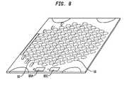
- FIG. 8illustrates an exemplary array 80 of diodes 10 , with buried interconnection circuitry (not shown) added to the ceramic ( 17 of FIG. 1 ) connected to common electrodes 81 A, 81 C.
- FIG. 9is a schematic cross section of an array 90 of LTCC-M packaged LED diodes 10 that is particularly easy to fabricate.
- array 90comprises a plurality of diodes 10 disposed between a heat sink 91 and an apertured PC board 92 .
- the light emitting portion of each LED 10is aligned with a corresponding window aperture 93 of PC board 92 .
- the PC board 92advantageously contains the control and driver circuits (not shown) and electrical connections between the circuits and the LED's, e.g. connections 94 .
- the PC Board 92can be conveniently secured to the heat sink (which can be a sheet of aluminum), as by screws 95 , to hold the diodes 10 in thermal contact with the heat sink.
- Advantageously thermal coupling between the diodes and the heat sinkcan be facilitated by thermal grease.
- the array 90is particularly easy to fabricate. After forming PC board 92 and providing a plurality of LTCC-M packaged diodes 10 as described herein, the diodes can be surface mounted on the PC board with the light emitting portions aligned with apertures, and LED contacts aligned with PC board contacts. After solder reflow connection, the PC board 92 can be secured to the heat sink 91 by screws 95 . The apertures and LEDs can be arranged across the surface of the board to achieve any desired configuration of a two-dimensional array of LEDs.
- FIG. 10is a top view illustrating a first advantageous configuration of LEDs 10 forming a closely packed hexagonal array.
- the PC board 92includes common electrodes 81 A and 81 C.
- FIG. 11is a top view of a second advantageous configuration.
- the LEDsare distributed in a plurality of sets 111 A, 111 B, and 111 C in respective sectors around the circumference of a circle and in a set 111 D in the center of the circle, all to emulate a concentrated light source.
- FIG. 12shows an embodiment of the invention suitable for use as a plug in card.
- a plurality of cavities 122includes a plurality LED die 123 , 124 , and 125 .
- LED die 123 , 124 , and 125can be identical die (for increased luminosity), or they can be individual colors and lit in various patterns for single, or mixed color displays. They can also be lit in various combinations to give variable intensity or to show patterns.
- Card contact fingers 126 , 127 , 128 , and 129show an exemplary embodiment to control the displayed color.
- finger 129is an electrical common (common cathode or common anode), and fingers 126 , 127 , and 128 are each connected to a single color die in each well to cause the card to light red, green, or blue respectively.
- each LED dieis wired to the respective LED die of the same color in each well and to the respective control finger for that color.
- decoding/driver electronicscan be embedded directly in the layers of the card and can control individual LED die or groups of die.
- FIG. 13shows card advantageously mounted on heat sink 132 for additional cooling. Also the card is shown plugged into edge connector 133 showing how contact is made with contact fingers 126 , 127 , 128 .
- FIGS. 14 and 15are top views showing flip-chip die 143 in LTCC-M package 141 .
- FIG. 15is a side view of the same assembly showing flip chip 143 connected to a wiring plane on surface 142 by bumps 144 .
- FIG. 16shows a top view of a package before the die is installed. Wiring traces 161 can be seen residing on surface 142 .
- connections to the LED assemblycan be made by isolated terminals 175 on base 174 . Openings in insulating layer 171 form wells for the LEDs as before. Insulating layer 171 can optionally include ground plane 172 . Metal vias 173 can facilitate electrical connections from isolated terminals 175 to the die via conductive traces (not shown).
- FIG. 18shows a version of this embodiment designed to house a plurality of die 10 .
- This partwas built using a 13% copper, 74% molybdenum, 13% copper (CMC) metal laminate produced by H.C. Starck Corp. Thick film gold bonding pads are fired on the metal base to correspond to the location of each diode electrode. The pads are connected electrically and thermally to the CMC base. 4 layers of CMC-compatible ceramic tape are used to form the LED cavities, make the electrical connections, and form the array housing.
- the ceramic tapeis composed of glasses and resins supplied by Ferro Corp. and others. The tape materials are ground, mixed, and cast into flat sheets. The sheets are then processed using common “green” tape processing including punching, printing, collating, and laminating.
- the cavitiesare formed by routing (cutting away material with a rotary tool), pressing the shape using a rigid tool during lamination in the green state, or by punching the cavity in each ceramic layer (green-state punching) using a round punch tool 190 with punch shaft 191 and tapered shaft 192 ( FIG. 19 ).
- Round Punch 193pushes out the ceramic tape chad, then the tapered shaft 192 presses a taper into the green tape.
- the surfaceis optionally coated with a silver or aluminum metal powder prior to each punch. During the punching operation the metal powder is transferred to the ceramic tape. When fired, the metal sinters into the ceramic.
- the surface of the tapercan also be polished after firing using a rotary polishing tool.
- a polished surfacecan also result by using a ceramic powder with a finer grain size in the production of the ceramic tape. The finer grain size reduces the surface roughness of the finished part.
- the CMC baseis attached during lamination and joined to the tape layers during firing at ⁇ 900° C. Multiple arrays are processed on a single wafer, which is then singulated by dicing after firing. After the package is complete, individual diodes are connected to the gold pads in the bottom of each cavity by soldering using 80% Au/20% Sn solder, or using electrically conductive epoxy such as Ablebond 84LMI. The gold pads are connected to the metal base. Conductive vias connect an electrical terminal on the top ceramic layer to the metal base. The anode or cathode are commonly connected to the back side of the diode which is in-turn connected to the gold bonding pad The opposite side of the diode is electrically connected to the array using a wire bond.
- the bondis connected from the diode to a bonding pad on one of the ceramic layers.
- conductive tracesare deposited onto the surface of the ceramic layer containing the bonding pads.
- the tracesare connected to an electrical terminal on the top ceramic layer through electrically conductive vias.
- a variety of diode connectionsare possible including series, parallel, and combined series-parallel.
- Voltage dropping and current limiting resistors, inductors, and capacitorsmay be added as components buried in between the ceramic layers, or as discrete components mounted on the top surface of the package. Additional control, ESD protection, and voltage regulation semiconductors may be added in die or packaged form.
- an index matching epoxysuch as Hysol 1600, may be added to each diode cavity to improve the light output of each device, followed by a cover or lens that may be attached using clear Hysol 1600.
- Multilayer ceramic circuit boardsare made from layers of green ceramic tapes.
- a green tapeis made from particular glass compositions and optional ceramic powders, which are mixed with organic binders and a solvent, cast and cut to form the tape.
- Wiring patternscan be screen printed onto the tape layers to carry out various functions. Vias are then punched in the tape and are filled with a conductor ink to connect the wiring on one green tape to wiring on another green tape. The tapes are then aligned, laminated, and fired to remove the organic materials, to sinter the metal patterns and to crystallize the glasses. This is generally carried out at temperatures below about 1000° C., and preferably from about 750–950° C.
- the composition of the glassesdetermines the coefficient of thermal expansion, the dielectric constant and the compatibility of the multilayer ceramic circuit boards to various electronic components.
- Exemplary crystallizing glasses with inorganic fillers that sinter in the temperature range 700 to 1000° C.are Magnesium Alumino-Silicate, Calcium Boro-Silicate, Lead Boro-Silicate, and Calcium Alumino-Boricate.
- metal support substratesmetal boards
- the metal boardslend strength to the glass layers.
- the green tape layerscan be mounted on both sides of a metal board and can be adhered to a metal board with suitable bonding glasses, the metal boards permit increased complexity and density of circuits and devices.
- passive and active componentssuch as resistors, inductors, and capacitors can be incorporated into the circuit boards for additional functionality.
- optical componentssuch as LEDs are installed, the walls of the ceramic layers can be shaped and/or coated to enhance the reflective optical properties of the package.
- LTCC-Mlow temperature cofired ceramic-metal support boards
- LTCC-Mlow temperature cofired ceramic-metal support boards
- the systemcan be tailored to be compatible with devices including silicon-based devices, indium phosphide-based devices and gallium arsenide-based devices, for example, by proper choice of the metal for the support board and of the glasses in the green tapes.
- the ceramic layers of the LTCC-M structuremust be matched to the thermal coefficient of expansion of the metal support board. Glass ceramic compositions are known that match the thermal expansion properties of various metal or metal matrix composites.
- the LTCC-M structure and materialsare described in U.S. Pat. No. 6,455,930, “Integrated heat sinking packages using low temperature co-fired ceramic metal circuit board technology”, issued Sep. 24, 2002 to Ponnuswamy, et al and assigned to Lamina Ceramics. U.S. Pat. No. 6,455,930 is incorporated by reference herein.
- the LTCC-M structureis further described in U.S. Pat. Nos. 5,581,876, 5,725,808, 5,953,203, and 6,518,502, all of which are assigned to Lamina Ceramics and also incorporated by reference herein.
- metal support boards used for LTCC-M technologydo have a high thermal conductivity, but some metal boards have a high thermal coefficient of expansion, and thus a bare die cannot always be directly mounted to such metal support boards.
- some metal support boardsare known that can be used for such purposes, such as metal composites of copper and molybdenum (including from 10–25% by weight of copper) or copper and tungsten (including 10–25% by weight of copper), made using powder metallurgical techniques.
- Copper clad Kovar®a metal alloy of iron, nickel, cobalt and manganese, a trademark of Carpenter Technology, is a very useful support board.
- AlSiCis another material that can be used for direct attachment, as can aluminum or copper graphite composites.
- FIGS. 14 and 15show the inventive LED system where the LTCC-M package house LED die.
- Densely packed microcircuitry, and devices such as decoder/drivers, amplifiers, oscillators and the like which generate large amounts of heat,can also use LTCC-M techniques advantageously.
- Metallization on the top layers of an integrated circuitbring input/output lines to the edge of the chip so as to be able to wire bond to the package or module that contains the chip. Thus the length of the wirebond wire becomes an issue; too long a wire leads to parasitics.
- the cost of very high integration chipsmay be determined by the arrangement of the bond pads, rather than by the area of silicon needed to create the circuitry.
- Flip chip packagingovercomes at least some of these problems by using solder bumps rather than wirebond pads to make connections. These solder bumps are smaller than wire bond pads and, when the chip is turned upside down, or flipped, solder reflow can be used to attach the chip to the package. Since the solder bumps are small, the chip can contain input/output connections within its interior if multilayer packaging is used. Thus the number of transistors in it, rather than the number and size of bond pads will determine the chip size.
- heat sinksare the small solder bumps that connect the chip to the package. If this is insufficient, small active or passive heat sinks must be added on top of the flip chip. Such additional heat sinks increase assembly costs, increase the number of parts required, and increase the package costs. Particularly if the heat sinks have a small thermal mass, they have limited effectiveness as well.
- LTCC-M technologyis used to provide an integrated package for a semiconductor component and accompanying circuitry, wherein the conductive metal support board provides a heat sink for the component.
- a bare semiconductor diefor example, can be mounted directly onto a metal base of the LTCC-M system having high thermal conductivity to cool the semiconductor component.
- the electrical signals to operate the componentmust be connected to the component from the ceramic.
- wire bond 54serves this purpose. Indirect attachment to the metal support board can also be used.
- the required componentsare mounted on a metal support board, incorporating embedded passive components such as conductors and resistors into the multilayer ceramic portion, to connect the various components, i.e., semiconductor components, circuits, heat sink and the like, in an integrated package.
- the packagecan be hermetically sealed with a lid.
- the integrated package of the inventioncombines a first and a second LTCC-M substrate.
- the first substratecan have mounted thereon a semiconductor device, and a multilayer ceramic circuit board with embedded circuitry for operating the component; the second substrate has a heat sink or conductive heat spreader mounted thereon.
- Thermoelectric (TEC) plates(Peltier devices) and temperature control circuitry are mounted between the first and second substrates to provide improved temperature control of semiconductor devices.
- TECthermoelectric
- a hermetic enclosurecan be adhered to the metal support board.
- LTCC-M technologycan also utilize the advantages of flip chip packaging together with integrated heat sinking.
- the packages of the inventioncan be made smaller, cheaper and more efficient than existing present-day packaging.
- the metal substrateserves as a heat spreader or heat sink.
- the flip chipcan be mounted directly on the metal substrate, which is an integral part of the package, eliminating the need for additional heat sinking.
- a flexible circuitcan be mounted over the bumps on the flip chip.
- the use of multilayer ceramic layerscan also accomplish a fan-out and routing of traces to the periphery of the package, further improving heat sinking. High power integrated circuits and devices that have high thermal management needs can be used with this new LTCC-M technology.
Landscapes
- Engineering & Computer Science (AREA)
- Power Engineering (AREA)
- Microelectronics & Electronic Packaging (AREA)
- Physics & Mathematics (AREA)
- Condensed Matter Physics & Semiconductors (AREA)
- General Physics & Mathematics (AREA)
- Computer Hardware Design (AREA)
- Led Device Packages (AREA)
Abstract
Description
Claims (30)
Priority Applications (14)
| Application Number | Priority Date | Filing Date | Title |
|---|---|---|---|
| US10/638,579US7095053B2 (en) | 2003-05-05 | 2003-08-11 | Light emitting diodes packaged for high temperature operation |
| PCT/US2004/012746WO2004100343A2 (en) | 2003-05-05 | 2004-04-26 | Light emitting diodes packaged for high temperature operation |
| JP2006513307AJP4912876B2 (en) | 2003-05-05 | 2004-04-26 | Light emitting diode packaged for high temperature operation |
| EP04750631AEP1620896A2 (en) | 2003-05-05 | 2004-04-26 | Light emitting diodes packaged for high temperature operation |
| KR1020057020831AKR101095291B1 (en) | 2003-05-05 | 2004-04-26 | Packaged Light Emitting Diodes for High Temperature Operation |
| US10/933,096US7098483B2 (en) | 2003-05-05 | 2004-09-02 | Light emitting diodes packaged for high temperature operation |
| US11/030,648US7300182B2 (en) | 2003-05-05 | 2005-01-06 | LED light sources for image projection systems |
| US11/083,862US7176502B2 (en) | 2003-05-05 | 2005-03-18 | Light emitting diodes packaged for high temperature operation |
| US11/179,863US7528421B2 (en) | 2003-05-05 | 2005-07-12 | Surface mountable light emitting diode assemblies packaged for high temperature operation |
| US11/343,986US7633093B2 (en) | 2003-05-05 | 2006-01-31 | Method of making optical light engines with elevated LEDs and resulting product |
| US11/409,847US7777235B2 (en) | 2003-05-05 | 2006-04-24 | Light emitting diodes with improved light collimation |
| US11/445,611US20070013057A1 (en) | 2003-05-05 | 2006-06-02 | Multicolor LED assembly with improved color mixing |
| US11/875,555US20080035938A1 (en) | 2003-05-05 | 2007-10-19 | Thermally coupled light source for an image projection system |
| US13/416,146US20120195037A1 (en) | 2003-05-05 | 2012-03-09 | Led light sources for image projection systems |
Applications Claiming Priority (2)
| Application Number | Priority Date | Filing Date | Title |
|---|---|---|---|
| US46785703P | 2003-05-05 | 2003-05-05 | |
| US10/638,579US7095053B2 (en) | 2003-05-05 | 2003-08-11 | Light emitting diodes packaged for high temperature operation |
Related Child Applications (7)
| Application Number | Title | Priority Date | Filing Date |
|---|---|---|---|
| US10/933,096DivisionUS7098483B2 (en) | 2003-05-05 | 2004-09-02 | Light emitting diodes packaged for high temperature operation |
| US11/030,648Continuation-In-PartUS7300182B2 (en) | 2003-05-05 | 2005-01-06 | LED light sources for image projection systems |
| US11/083,862DivisionUS7176502B2 (en) | 2003-05-05 | 2005-03-18 | Light emitting diodes packaged for high temperature operation |
| US11/179,863Continuation-In-PartUS7528421B2 (en) | 2003-05-05 | 2005-07-12 | Surface mountable light emitting diode assemblies packaged for high temperature operation |
| US11/343,986Continuation-In-PartUS7633093B2 (en) | 2003-05-05 | 2006-01-31 | Method of making optical light engines with elevated LEDs and resulting product |
| US11/409,847Continuation-In-PartUS7777235B2 (en) | 2003-05-05 | 2006-04-24 | Light emitting diodes with improved light collimation |
| US11/445,611Continuation-In-PartUS20070013057A1 (en) | 2003-05-05 | 2006-06-02 | Multicolor LED assembly with improved color mixing |
Publications (2)
| Publication Number | Publication Date |
|---|---|
| US20040222433A1 US20040222433A1 (en) | 2004-11-11 |
| US7095053B2true US7095053B2 (en) | 2006-08-22 |
Family
ID=33423666
Family Applications (3)
| Application Number | Title | Priority Date | Filing Date |
|---|---|---|---|
| US10/638,579Expired - LifetimeUS7095053B2 (en) | 2003-05-05 | 2003-08-11 | Light emitting diodes packaged for high temperature operation |
| US10/933,096Expired - LifetimeUS7098483B2 (en) | 2003-05-05 | 2004-09-02 | Light emitting diodes packaged for high temperature operation |
| US11/083,862Expired - LifetimeUS7176502B2 (en) | 2003-05-05 | 2005-03-18 | Light emitting diodes packaged for high temperature operation |
Family Applications After (2)
| Application Number | Title | Priority Date | Filing Date |
|---|---|---|---|
| US10/933,096Expired - LifetimeUS7098483B2 (en) | 2003-05-05 | 2004-09-02 | Light emitting diodes packaged for high temperature operation |
| US11/083,862Expired - LifetimeUS7176502B2 (en) | 2003-05-05 | 2005-03-18 | Light emitting diodes packaged for high temperature operation |
Country Status (5)
| Country | Link |
|---|---|
| US (3) | US7095053B2 (en) |
| EP (1) | EP1620896A2 (en) |
| JP (1) | JP4912876B2 (en) |
| KR (1) | KR101095291B1 (en) |
| WO (1) | WO2004100343A2 (en) |
Cited By (77)
| Publication number | Priority date | Publication date | Assignee | Title |
|---|---|---|---|---|
| US20050247945A1 (en)* | 2004-05-10 | 2005-11-10 | United Epitaxy Company, Ltd. | LED heat-radiating substrate and method for making the same |
| US20050274959A1 (en)* | 2004-06-10 | 2005-12-15 | Geun-Ho Kim | High power LED package |
| US20060006405A1 (en)* | 2003-05-05 | 2006-01-12 | Lamina Ceramics, Inc. | Surface mountable light emitting diode assemblies packaged for high temperature operation |
| US20060012034A1 (en)* | 2004-07-13 | 2006-01-19 | Hitachi, Ltd. | Engine control circuit device |
| US20060027829A1 (en)* | 2003-03-18 | 2006-02-09 | Pai-Hsiang Wang | Package structure for light emitting diode and method thereof |
| US20060078246A1 (en)* | 2004-10-07 | 2006-04-13 | Towa Corporation | Transparent member, optical device using transparent member and method of manufacturing optical device |
| US20060180821A1 (en)* | 2003-06-30 | 2006-08-17 | Koninklijke Philips Electronics N.V. | Light-emitting diode thermal management system |
| US20060261357A1 (en)* | 2005-05-18 | 2006-11-23 | Ching-Fu Tsou | Array-type modularized light-emitting diode structure and a method for packaging the structure |
| US20070013057A1 (en)* | 2003-05-05 | 2007-01-18 | Joseph Mazzochette | Multicolor LED assembly with improved color mixing |
| US20070013090A1 (en)* | 2005-07-12 | 2007-01-18 | Shinji Takase | Method of resin-sealing and molding an optical device |
| US20070040163A1 (en)* | 2005-08-18 | 2007-02-22 | Tdk Corporation | Electronic component and method of manufacturing the same |
| US20070085101A1 (en)* | 2005-10-19 | 2007-04-19 | Lg Innotek Co., Ltd. | Light emitting diode package |
| US20070103875A1 (en)* | 2005-11-04 | 2007-05-10 | Reis Bradley E | Cycling LED Heat Spreader |
| US20070132135A1 (en)* | 2004-04-26 | 2007-06-14 | Towa Corporation | Manufacturing method of optical electronic components and optical electronic components manufactured using the same |
| US20070263389A1 (en)* | 2006-03-17 | 2007-11-15 | Elit Fine Ceramics Co., Ltd. | LED reflector molding process, construction, and loader thereof |
| US20070291482A1 (en)* | 2006-06-16 | 2007-12-20 | Tajul Arosh Baroky | Illumination device and method of making the device |
| US20070291489A1 (en)* | 2006-06-16 | 2007-12-20 | Tajul Arosh Baroky | Light source device and method of making the device |
| US20080043444A1 (en)* | 2004-04-27 | 2008-02-21 | Kyocera Corporation | Wiring Board for Light-Emitting Element |
| US20080133782A1 (en)* | 2006-12-01 | 2008-06-05 | Lg Electronics Inc. | Reception system and method of processing interface information |
| US20080239675A1 (en)* | 2005-01-05 | 2008-10-02 | Tir Systems Ltd. | Thermally and Electrically Conductive Apparatus |
| US20090050908A1 (en)* | 2005-01-10 | 2009-02-26 | Cree, Inc. | Solid state lighting component |
| US20090140285A1 (en)* | 2007-11-30 | 2009-06-04 | Advanced Connectek Inc. | Light emitting device having function of heat-dissipation and manufacturing process for such device |
| US20090195159A1 (en)* | 2008-02-03 | 2009-08-06 | Smith Jerry L | Led cooling system |
| US20090278162A1 (en)* | 2005-09-01 | 2009-11-12 | E.I. Du Pont De Nemours And Company | Low Temperature Co-Fired Ceramic (LTCC) Tape Compositions, Light-Emitting Diode (LED) Modules, Lighting Devices and Methods of Forming Thereof |
| US20090309106A1 (en)* | 2005-06-03 | 2009-12-17 | Shen-Nan Tong | Light-emitting device module with a substrate and methods of forming it |
| US20100127283A1 (en)* | 2008-10-24 | 2010-05-27 | Van De Ven Antony P | Array layout for color mixing |
| US7777235B2 (en) | 2003-05-05 | 2010-08-17 | Lighting Science Group Corporation | Light emitting diodes with improved light collimation |
| US20110043137A1 (en)* | 2009-08-19 | 2011-02-24 | Cree Led Lighting Solutions, Inc. | White light color changing solid state lighting and methods |
| US20110148327A1 (en)* | 2009-12-21 | 2011-06-23 | Van De Ven Antony P | High cri adjustable color temperature lighting devices |
| US8044412B2 (en) | 2006-01-20 | 2011-10-25 | Taiwan Semiconductor Manufacturing Company, Ltd | Package for a light emitting element |
| US20120092833A1 (en)* | 2010-10-13 | 2012-04-19 | Ho Cheng Industrial Co., Ltd. | Led heat-conducting substrate and its thermal module |
| US8253336B2 (en) | 2010-07-23 | 2012-08-28 | Biological Illumination, Llc | LED lamp for producing biologically-corrected light |
| US8324808B2 (en) | 2010-07-23 | 2012-12-04 | Biological Illumination, Llc | LED lamp for producing biologically-corrected light |
| US20130009191A1 (en)* | 2011-07-04 | 2013-01-10 | Lite-On Singapore Pte. Ltd. | Surface mounted led package and manufacturing method therefor |
| US20130026924A1 (en)* | 2011-01-28 | 2013-01-31 | Seoul Semiconductor Co., Ltd. | Led driving circuit package |
| US20130069218A1 (en)* | 2011-09-20 | 2013-03-21 | Stmicroelectronics Asia Pacific Pte Ltd. | High density package interconnect with copper heat spreader and method of making the same |
| US8415704B2 (en) | 2010-09-22 | 2013-04-09 | Ut-Battelle, Llc | Close-packed array of light emitting devices |
| US20140011309A1 (en)* | 2010-12-22 | 2014-01-09 | Francois Lechleiter | Circuit for a Light Emitting Component and Method of Manufacturing the Same |
| USD700584S1 (en) | 2011-07-06 | 2014-03-04 | Cree, Inc. | LED component |
| US8680457B2 (en) | 2012-05-07 | 2014-03-25 | Lighting Science Group Corporation | Motion detection system and associated methods having at least one LED of second set of LEDs to vary its voltage |
| US8686641B2 (en) | 2011-12-05 | 2014-04-01 | Biological Illumination, Llc | Tunable LED lamp for producing biologically-adjusted light |
| US8698171B2 (en) | 2005-01-10 | 2014-04-15 | Cree, Inc. | Solid state lighting component |
| US8743023B2 (en) | 2010-07-23 | 2014-06-03 | Biological Illumination, Llc | System for generating non-homogenous biologically-adjusted light and associated methods |
| US8754832B2 (en) | 2011-05-15 | 2014-06-17 | Lighting Science Group Corporation | Lighting system for accenting regions of a layer and associated methods |
| US20140167093A1 (en)* | 2012-12-13 | 2014-06-19 | Hon Hai Precision Industry Co., Ltd. | Light emitting diode having a plurality of heat conductive columns |
| US8760370B2 (en) | 2011-05-15 | 2014-06-24 | Lighting Science Group Corporation | System for generating non-homogenous light and associated methods |
| US8761447B2 (en) | 2010-11-09 | 2014-06-24 | Biological Illumination, Llc | Sustainable outdoor lighting system for use in environmentally photo-sensitive area |
| US8841864B2 (en) | 2011-12-05 | 2014-09-23 | Biological Illumination, Llc | Tunable LED lamp for producing biologically-adjusted light |
| US8866414B2 (en) | 2011-12-05 | 2014-10-21 | Biological Illumination, Llc | Tunable LED lamp for producing biologically-adjusted light |
| US8901850B2 (en) | 2012-05-06 | 2014-12-02 | Lighting Science Group Corporation | Adaptive anti-glare light system and associated methods |
| US8963450B2 (en) | 2011-12-05 | 2015-02-24 | Biological Illumination, Llc | Adaptable biologically-adjusted indirect lighting device and associated methods |
| USD723729S1 (en) | 2013-03-15 | 2015-03-03 | Lighting Science Group Corporation | Low bay luminaire |
| US9006987B2 (en) | 2012-05-07 | 2015-04-14 | Lighting Science Group, Inc. | Wall-mountable luminaire and associated systems and methods |
| US9024536B2 (en) | 2011-12-05 | 2015-05-05 | Biological Illumination, Llc | Tunable LED lamp for producing biologically-adjusted light and associated methods |
| US9173269B2 (en) | 2011-05-15 | 2015-10-27 | Lighting Science Group Corporation | Lighting system for accentuating regions of a layer and associated methods |
| US9174067B2 (en) | 2012-10-15 | 2015-11-03 | Biological Illumination, Llc | System for treating light treatable conditions and associated methods |
| US9220202B2 (en) | 2011-12-05 | 2015-12-29 | Biological Illumination, Llc | Lighting system to control the circadian rhythm of agricultural products and associated methods |
| US9289574B2 (en) | 2011-12-05 | 2016-03-22 | Biological Illumination, Llc | Three-channel tuned LED lamp for producing biologically-adjusted light |
| US9335006B2 (en) | 2006-04-18 | 2016-05-10 | Cree, Inc. | Saturated yellow phosphor converted LED and blue converted red LED |
| US9347655B2 (en) | 2013-03-11 | 2016-05-24 | Lighting Science Group Corporation | Rotatable lighting device |
| US9402294B2 (en) | 2012-05-08 | 2016-07-26 | Lighting Science Group Corporation | Self-calibrating multi-directional security luminaire and associated methods |
| US9532423B2 (en) | 2010-07-23 | 2016-12-27 | Lighting Science Group Corporation | System and methods for operating a lighting device |
| US9681522B2 (en) | 2012-05-06 | 2017-06-13 | Lighting Science Group Corporation | Adaptive light system and associated methods |
| US9693414B2 (en) | 2011-12-05 | 2017-06-27 | Biological Illumination, Llc | LED lamp for producing biologically-adjusted light |
| US9704774B2 (en) | 2012-12-11 | 2017-07-11 | Sensor Electronic Technology, Inc. | Thermal management structure with integrated heat sink |
| US9786811B2 (en) | 2011-02-04 | 2017-10-10 | Cree, Inc. | Tilted emission LED array |
| US9827439B2 (en) | 2010-07-23 | 2017-11-28 | Biological Illumination, Llc | System for dynamically adjusting circadian rhythm responsive to scheduled events and associated methods |
| US10295147B2 (en) | 2006-11-09 | 2019-05-21 | Cree, Inc. | LED array and method for fabricating same |
| US10842016B2 (en) | 2011-07-06 | 2020-11-17 | Cree, Inc. | Compact optically efficient solid state light source with integrated thermal management |
| US10856470B2 (en) | 2017-09-19 | 2020-12-08 | Agnetix, Inc. | Fluid-cooled LED-based lighting methods and apparatus for controlled environment agriculture |
| US10959383B2 (en) | 2018-05-04 | 2021-03-30 | Agnetix, Inc. | Methods, apparatus, and systems for lighting and distributed sensing in controlled agricultural environments |
| US10999976B2 (en) | 2017-09-19 | 2021-05-11 | Agnetix, Inc. | Fluid-cooled lighting systems and kits for controlled agricultural environments, and methods for installing same |
| US11013078B2 (en) | 2017-09-19 | 2021-05-18 | Agnetix, Inc. | Integrated sensor assembly for LED-based controlled environment agriculture (CEA) lighting, and methods and apparatus employing same |
| US11076536B2 (en) | 2018-11-13 | 2021-08-03 | Agnetix, Inc. | Fluid-cooled LED-based lighting methods and apparatus for controlled environment agriculture with integrated cameras and/or sensors and wireless communications |
| US11791442B2 (en) | 2007-10-31 | 2023-10-17 | Creeled, Inc. | Light emitting diode package and method for fabricating same |
| US11982433B2 (en) | 2019-12-12 | 2024-05-14 | Agnetix, Inc. | Fluid-cooled LED-based lighting methods and apparatus in close proximity grow systems for Controlled Environment Horticulture |
| US12020430B2 (en) | 2019-12-10 | 2024-06-25 | Agnetix, Inc. | Multisensory imaging methods and apparatus for controlled environment horticulture using irradiators and cameras and/or sensors |
Families Citing this family (238)
| Publication number | Priority date | Publication date | Assignee | Title |
|---|---|---|---|---|
| JP2003309292A (en)* | 2002-04-15 | 2003-10-31 | Citizen Electronics Co Ltd | Metal core substrate for surface mounted light emitting diode and method of manufacturing the same |
| WO2003096387A2 (en) | 2002-05-08 | 2003-11-20 | Phoseon Technology, Inc. | High efficiency solid-state light source and methods of use and manufacture |
| TWI299559B (en)* | 2002-06-19 | 2008-08-01 | Inpaq Technology Co Ltd | Ic substrate with over voltage protection function and method for manufacturing the same |
| US7775685B2 (en)* | 2003-05-27 | 2010-08-17 | Cree, Inc. | Power surface mount light emitting die package |
| US7244965B2 (en)* | 2002-09-04 | 2007-07-17 | Cree Inc, | Power surface mount light emitting die package |
| US7298046B2 (en)* | 2003-01-10 | 2007-11-20 | Kyocera America, Inc. | Semiconductor package having non-ceramic based window frame |
| US7262550B2 (en) | 2003-04-15 | 2007-08-28 | Luminus Devices, Inc. | Light emitting diode utilizing a physical pattern |
| US7095053B2 (en)* | 2003-05-05 | 2006-08-22 | Lamina Ceramics, Inc. | Light emitting diodes packaged for high temperature operation |
| US7300182B2 (en)* | 2003-05-05 | 2007-11-27 | Lamina Lighting, Inc. | LED light sources for image projection systems |
| US7633093B2 (en)* | 2003-05-05 | 2009-12-15 | Lighting Science Group Corporation | Method of making optical light engines with elevated LEDs and resulting product |
| US7919787B2 (en)* | 2003-06-27 | 2011-04-05 | Avago Technologies Ecbu Ip (Singapore) Pte. Ltd. | Semiconductor device with a light emitting semiconductor die |
| US7211835B2 (en)* | 2003-07-09 | 2007-05-01 | Nichia Corporation | Light emitting device, method of manufacturing the same and lighting equipment |
| US7183587B2 (en)* | 2003-09-09 | 2007-02-27 | Cree, Inc. | Solid metal block mounting substrates for semiconductor light emitting devices |
| WO2005041632A2 (en) | 2003-10-31 | 2005-05-12 | Phoseon Technology, Inc. | Collection optics for led array with offset hemispherical or faceted surfaces |
| KR100586944B1 (en)* | 2003-12-26 | 2006-06-07 | 삼성전기주식회사 | High power light emitting diode package and manufacturing method |
| JP4312616B2 (en)* | 2004-01-26 | 2009-08-12 | Necエレクトロニクス株式会社 | Semiconductor device |
| US7279724B2 (en)* | 2004-02-25 | 2007-10-09 | Philips Lumileds Lighting Company, Llc | Ceramic substrate for a light emitting diode where the substrate incorporates ESD protection |
| US7964883B2 (en)* | 2004-02-26 | 2011-06-21 | Lighting Science Group Corporation | Light emitting diode package assembly that emulates the light pattern produced by an incandescent filament bulb |
| US7235878B2 (en) | 2004-03-18 | 2007-06-26 | Phoseon Technology, Inc. | Direct cooling of LEDs |
| WO2005091392A1 (en) | 2004-03-18 | 2005-09-29 | Phoseon Technology, Inc. | Micro-reflectors on a substrate for high-density led array |
| DE102004014207A1 (en)* | 2004-03-23 | 2005-10-13 | Osram Opto Semiconductors Gmbh | Optoelectronic component with a multi-part housing body |
| US20050225222A1 (en)* | 2004-04-09 | 2005-10-13 | Joseph Mazzochette | Light emitting diode arrays with improved light extraction |
| US8188503B2 (en) | 2004-05-10 | 2012-05-29 | Permlight Products, Inc. | Cuttable illuminated panel |
| US7329905B2 (en) | 2004-06-30 | 2008-02-12 | Cree, Inc. | Chip-scale methods for packaging light emitting devices and chip-scale packaged light emitting devices |
| US7252408B2 (en)* | 2004-07-19 | 2007-08-07 | Lamina Ceramics, Inc. | LED array package with internal feedback and control |
| JP4528062B2 (en)* | 2004-08-25 | 2010-08-18 | 富士通株式会社 | Semiconductor device and manufacturing method thereof |
| US7745832B2 (en) | 2004-09-24 | 2010-06-29 | Epistar Corporation | Semiconductor light-emitting element assembly with a composite substrate |
| JP4014591B2 (en)* | 2004-10-05 | 2007-11-28 | シャープ株式会社 | Semiconductor device and electronic equipment |
| US20060097385A1 (en) | 2004-10-25 | 2006-05-11 | Negley Gerald H | Solid metal block semiconductor light emitting device mounting substrates and packages including cavities and heat sinks, and methods of packaging same |
| KR100646093B1 (en)* | 2004-12-17 | 2006-11-15 | 엘지이노텍 주식회사 | Light emitting device package |
| US7322732B2 (en)* | 2004-12-23 | 2008-01-29 | Cree, Inc. | Light emitting diode arrays for direct backlighting of liquid crystal displays |
| EP1866954B1 (en) | 2004-12-30 | 2016-04-20 | Phoseon Technology, Inc. | Methods and systems relating to light sources for use in industrial processes |
| NL1027961C2 (en)* | 2005-01-05 | 2006-07-06 | Lemnis Lighting Ip Gmbh | Electrical circuit, use of a semiconductor component and method for manufacturing a semiconductor component. |
| US7304694B2 (en)* | 2005-01-12 | 2007-12-04 | Cree, Inc. | Solid colloidal dispersions for backlighting of liquid crystal displays |
| TWI261936B (en)* | 2005-01-25 | 2006-09-11 | Lustrous Technology Ltd | LED package structure and mass production method of making the same |
| KR101197046B1 (en)* | 2005-01-26 | 2012-11-06 | 삼성디스플레이 주식회사 | Two dimensional light source of using light emitting diode and liquid crystal display panel of using the two dimensional light source |
| US7525248B1 (en) | 2005-01-26 | 2009-04-28 | Ac Led Lighting, L.L.C. | Light emitting diode lamp |
| US7284882B2 (en)* | 2005-02-17 | 2007-10-23 | Federal-Mogul World Wide, Inc. | LED light module assembly |
| JP2006245336A (en)* | 2005-03-03 | 2006-09-14 | Koito Mfg Co Ltd | Light-emitting device |
| WO2006099741A1 (en)* | 2005-03-24 | 2006-09-28 | Tir Systems Ltd. | Solid-state lighting device package |
| KR100593935B1 (en)* | 2005-03-24 | 2006-06-30 | 삼성전기주식회사 | Light emitting diode package and manufacturing method thereof |
| WO2006105638A1 (en)* | 2005-04-05 | 2006-10-12 | Tir Systems Ltd. | Electronic device package with an integrated evaporator |
| JP2006294782A (en)* | 2005-04-08 | 2006-10-26 | Hitachi Ltd | Semiconductor light source device |
| US7918591B2 (en)* | 2005-05-13 | 2011-04-05 | Permlight Products, Inc. | LED-based luminaire |
| PL3770980T3 (en)* | 2005-05-20 | 2024-11-12 | Signify Holding B.V. | Lighting-emitting module |
| TW200702824A (en)* | 2005-06-02 | 2007-01-16 | Koninkl Philips Electronics Nv | LED assembly and module |
| US8272757B1 (en)* | 2005-06-03 | 2012-09-25 | Ac Led Lighting, L.L.C. | Light emitting diode lamp capable of high AC/DC voltage operation |
| TWI294694B (en)* | 2005-06-14 | 2008-03-11 | Ind Tech Res Inst | Led wafer-level chip scale packaging |
| US20060289887A1 (en)* | 2005-06-24 | 2006-12-28 | Jabil Circuit, Inc. | Surface mount light emitting diode (LED) assembly with improved power dissipation |
| US20060292747A1 (en)* | 2005-06-27 | 2006-12-28 | Loh Ban P | Top-surface-mount power light emitter with integral heat sink |
| WO2007002644A2 (en)* | 2005-06-27 | 2007-01-04 | Lamina Lighting, Inc. | Light emitting diode package and method for making same |
| US8079743B2 (en)* | 2005-06-28 | 2011-12-20 | Lighting Science Group Corporation | Display backlight with improved light coupling and mixing |
| US7719021B2 (en)* | 2005-06-28 | 2010-05-18 | Lighting Science Group Corporation | Light efficient LED assembly including a shaped reflective cavity and method for making same |
| TWI422044B (en)* | 2005-06-30 | 2014-01-01 | Cree Inc | Wafer-scale method for packaging light-emitting device and light-emitting device packaged by wafer scale |
| WO2007005003A1 (en)* | 2005-06-30 | 2007-01-11 | Lamina Ceramics, Inc. | Light emitting diode package assembly that emulates the light pattern produced by an incandescent filament bulb |
| US7249868B2 (en)* | 2005-07-07 | 2007-07-31 | Visteon Global Technologies, Inc. | Lamp housing with interior cooling by a thermoelectric device |
| KR100629521B1 (en)* | 2005-07-29 | 2006-09-28 | 삼성전자주식회사 | LED package and manufacturing method thereof and LED array module using same |
| KR20080037734A (en)* | 2005-08-23 | 2008-04-30 | 가부시끼가이샤 도시바 | Light emitting device and back light and liquid crystal display using the same |
| KR20080045235A (en)* | 2005-08-23 | 2008-05-22 | 코닌클리즈케 필립스 일렉트로닉스 엔.브이. | Method for manufacturing components and ceramic components having a three-dimensional structure in the surface area |
| US7196354B1 (en) | 2005-09-29 | 2007-03-27 | Luminus Devices, Inc. | Wavelength-converting light-emitting devices |
| CN1945822B (en)* | 2005-10-07 | 2012-05-23 | 日立麦克赛尔株式会社 | Semiconductor device, semiconductor module and semiconductor module producing method |
| US20090225541A1 (en)* | 2005-10-20 | 2009-09-10 | Showa Denko K.K. | Luminous device mounting substrate, luminous device mounting package, and planar light source device |
| TWM295339U (en)* | 2005-10-28 | 2006-08-01 | Turning Prec Ind Co Ltd | Multilayer LED package structure |
| US7505275B2 (en)* | 2005-11-04 | 2009-03-17 | Graftech International Holdings Inc. | LED with integral via |
| US7889502B1 (en)* | 2005-11-04 | 2011-02-15 | Graftech International Holdings Inc. | Heat spreading circuit assembly |
| KR101171186B1 (en)* | 2005-11-10 | 2012-08-06 | 삼성전자주식회사 | High luminance light emitting diode and liquid crystal display panel of using the same |
| JP5209177B2 (en)* | 2005-11-14 | 2013-06-12 | 新光電気工業株式会社 | Semiconductor device and manufacturing method of semiconductor device |
| JP5113329B2 (en)* | 2005-11-25 | 2013-01-09 | パナソニック株式会社 | Light emitting device |
| US20070120138A1 (en)* | 2005-11-28 | 2007-05-31 | Visteon Global Technologies, Inc. | Multi-layer light emitting device with integrated thermoelectric chip |
| US7528422B2 (en)* | 2006-01-20 | 2009-05-05 | Hymite A/S | Package for a light emitting element with integrated electrostatic discharge protection |
| CA2540268A1 (en)* | 2006-03-22 | 2007-09-22 | Realights Inc. | Lighting process by insertion of electroluminescent diodes in acrylic |
| JP4908041B2 (en)* | 2006-03-31 | 2012-04-04 | 株式会社沖データ | Light emitting diode array, LED head, and image recording apparatus |
| US20070235739A1 (en)* | 2006-03-31 | 2007-10-11 | Edison Opto Corporation | Structure of heat dissipation of implant type light emitting diode package and method for manufacturing the same |
| JP2007294863A (en)* | 2006-03-31 | 2007-11-08 | Sanyo Electric Co Ltd | Circuit apparatus |
| DE102006018161A1 (en)* | 2006-04-19 | 2007-10-25 | Patent-Treuhand-Gesellschaft für elektrische Glühlampen mbH | Electronic component module |
| WO2007126074A1 (en)* | 2006-04-28 | 2007-11-08 | Shimane Prefectural Government | Semiconductor light emitting module, device, and its manufacturing method |
| CN100536180C (en)* | 2006-05-23 | 2009-09-02 | 台达电子工业股份有限公司 | light emitting device |
| WO2007139781A2 (en) | 2006-05-23 | 2007-12-06 | Cree Led Lighting Solutions, Inc. | Lighting device |
| JP4946195B2 (en)* | 2006-06-19 | 2012-06-06 | サンケン電気株式会社 | Semiconductor light emitting device and manufacturing method thereof |
| US7906794B2 (en)* | 2006-07-05 | 2011-03-15 | Koninklijke Philips Electronics N.V. | Light emitting device package with frame and optically transmissive element |
| US7732233B2 (en)* | 2006-07-24 | 2010-06-08 | Touch Micro-System Technology Corp. | Method for making light emitting diode chip package |
| US20090273004A1 (en)* | 2006-07-24 | 2009-11-05 | Hung-Yi Lin | Chip package structure and method of making the same |
| TWI320237B (en)* | 2006-07-24 | 2010-02-01 | Si-substrate and structure of opto-electronic package having the same | |
| US20090273005A1 (en)* | 2006-07-24 | 2009-11-05 | Hung-Yi Lin | Opto-electronic package structure having silicon-substrate and method of forming the same |
| US20080023715A1 (en)* | 2006-07-28 | 2008-01-31 | Choi Hoi Wai | Method of Making White Light LEDs and Continuously Color Tunable LEDs |
| TW200810145A (en)* | 2006-08-04 | 2008-02-16 | Chiang Cheng Ting | A lighting structure with light emitting diodes and the method thereof |
| CN100397669C (en)* | 2006-08-07 | 2008-06-25 | 陈盈君 | A preparation method of LED light source using low temperature co-fired ceramics designed by thermoelectric separation |
| KR100796522B1 (en)* | 2006-09-05 | 2008-01-21 | 삼성전기주식회사 | Manufacturing Method of Electronic Circuit Board |
| US20080074884A1 (en)* | 2006-09-25 | 2008-03-27 | Thye Linn Mok | Compact high-intensty LED-based light source and method for making the same |
| US8148746B2 (en)* | 2006-09-29 | 2012-04-03 | Rohm Co., Ltd. | Semiconductor light emitting device |
| US7714348B2 (en)* | 2006-10-06 | 2010-05-11 | Ac-Led Lighting, L.L.C. | AC/DC light emitting diodes with integrated protection mechanism |
| CN100510522C (en)* | 2006-10-25 | 2009-07-08 | 南茂科技股份有限公司 | Light source assembly |
| BRPI0718086A2 (en)* | 2006-10-31 | 2013-11-05 | Tir Technology Lp | LIGHTING DEVICE PACKAGING |
| US7667378B2 (en)* | 2006-11-14 | 2010-02-23 | Epson Imaging Devices Corporation | Illuminating device, electro-optic device, and electronic apparatus |
| TWI320608B (en)* | 2006-12-06 | 2010-02-11 | Chipmos Technologies Inc | Light emitting chip package and light source module |
| WO2008078237A2 (en) | 2006-12-21 | 2008-07-03 | Koninklijke Philips Electronics N.V. | Carrier and optical semiconductor device based on such a carrier |
| JP2008166440A (en)* | 2006-12-27 | 2008-07-17 | Spansion Llc | Semiconductor device |
| KR100851183B1 (en)* | 2006-12-27 | 2008-08-08 | 엘지이노텍 주식회사 | Semiconductor light emitting device package |
| US20080158886A1 (en)* | 2006-12-29 | 2008-07-03 | Siew It Pang | Compact High-Intensity LED Based Light Source |
| US7576425B2 (en)* | 2007-01-25 | 2009-08-18 | Xintec, Inc. | Conducting layer in chip package module |
| US9711703B2 (en) | 2007-02-12 | 2017-07-18 | Cree Huizhou Opto Limited | Apparatus, system and method for use in mounting electronic elements |
| US7510400B2 (en)* | 2007-03-14 | 2009-03-31 | Visteon Global Technologies, Inc. | LED interconnect spring clip assembly |
| JP4753904B2 (en) | 2007-03-15 | 2011-08-24 | シャープ株式会社 | Light emitting device |
| KR20080092599A (en)* | 2007-04-12 | 2008-10-16 | 엘지이노텍 주식회사 | Full Color LED Control Backlight Unit |
| KR100825766B1 (en)* | 2007-04-26 | 2008-04-29 | 한국전자통신연구원 | LTC package and manufacturing method |
| JP2010527158A (en)* | 2007-05-08 | 2010-08-05 | オッカム ポートフォリオ リミテッド ライアビリティ カンパニー | Solderless light emitting diode assembly |
| CN101312226B (en)* | 2007-05-24 | 2010-07-21 | 钜亨电子材料元件有限公司 | Light emitting diode seat structure with horizontal heat diffusion piece |
| EP1998101B2 (en) | 2007-05-30 | 2019-09-25 | OSRAM GmbH | Lighting device |
| US7942556B2 (en)* | 2007-06-18 | 2011-05-17 | Xicato, Inc. | Solid state illumination device |
| US20090008662A1 (en)* | 2007-07-05 | 2009-01-08 | Ian Ashdown | Lighting device package |
| US7621752B2 (en)* | 2007-07-17 | 2009-11-24 | Visteon Global Technologies, Inc. | LED interconnection integrated connector holder package |
| KR20090015734A (en)* | 2007-08-09 | 2009-02-12 | 엘지이노텍 주식회사 | Light source device |
| GB2455489B (en)* | 2007-08-22 | 2012-05-30 | Photonstar Led Ltd | High thermal performance packaging for optoelectronics devices |
| TWI356486B (en)* | 2007-09-07 | 2012-01-11 | Young Lighting Technology | Led light source module and manufacturing method t |
| JP4809308B2 (en)* | 2007-09-21 | 2011-11-09 | 新光電気工業株式会社 | Substrate manufacturing method |
| TW200917518A (en)* | 2007-10-05 | 2009-04-16 | Delta Electronics Inc | Co-fired ceramic module |
| JP2009094409A (en)* | 2007-10-11 | 2009-04-30 | Shinko Electric Ind Co Ltd | Semiconductor package and its manufacturing method |
| CN100546058C (en)* | 2007-10-15 | 2009-09-30 | 佛山市国星光电股份有限公司 | Power luminous diode packaging structure |
| WO2009054177A1 (en)* | 2007-10-24 | 2009-04-30 | Sharp Kabushiki Kaisha | Illuminating device for display device, display device, and television receiver |
| TW200928203A (en)* | 2007-12-24 | 2009-07-01 | Guei-Fang Chen | LED illuminating device capable of quickly dissipating heat and its manufacturing method |
| CN101469845B (en)* | 2007-12-29 | 2011-08-24 | 富士迈半导体精密工业(上海)有限公司 | Lighting device and its power supply module, and lamps using the lighting device |
| WO2009096619A1 (en)* | 2008-02-01 | 2009-08-06 | Ytel Photonics Inc. | Optical device package and method for manufacturing thereof |
| JP5146256B2 (en)* | 2008-03-18 | 2013-02-20 | 富士通株式会社 | Sheet-like structure and manufacturing method thereof, and electronic device and manufacturing method thereof |
| KR100982986B1 (en)* | 2008-04-17 | 2010-09-17 | 삼성엘이디 주식회사 | Submount, LED Package and Manufacturing Method Thereof |
| DE102008021435A1 (en)* | 2008-04-29 | 2009-11-19 | Schott Ag | Housing for LEDs with high performance |
| KR100992778B1 (en) | 2008-05-23 | 2010-11-05 | 엘지이노텍 주식회사 | Light emitting device package and method for manufacturing the same |
| JP5549104B2 (en)* | 2008-05-29 | 2014-07-16 | 株式会社リコー | Light emitting device, optical scanning device, and image forming apparatus |
| KR101438826B1 (en)* | 2008-06-23 | 2014-09-05 | 엘지이노텍 주식회사 | Light emitting device |
| US20100006886A1 (en)* | 2008-07-10 | 2010-01-14 | Brilliant Technology Co., Ltd. | High power light emitting diode chip package carrier structure |
| US8492179B2 (en)* | 2008-07-11 | 2013-07-23 | Koninklijke Philips N.V. | Method of mounting a LED module to a heat sink |
| GB2458972B (en)* | 2008-08-05 | 2010-09-01 | Photonstar Led Ltd | Thermally optimised led chip-on-board module |
| DE102008047100A1 (en)* | 2008-09-12 | 2010-03-25 | W.C. Heraeus Gmbh | Substrate for development of electronic components, particularly light emitting diode from punched copper-colored metal foil and non-metallic foil, includes coating copper-colored metal foil with metal |
| US8022626B2 (en)* | 2008-09-16 | 2011-09-20 | Osram Sylvania Inc. | Lighting module |
| US8183585B2 (en) | 2008-09-16 | 2012-05-22 | Osram Sylvania Inc. | Lighting module |
| US8188486B2 (en)* | 2008-09-16 | 2012-05-29 | Osram Sylvania Inc. | Optical disk for lighting module |
| US8203266B2 (en)* | 2008-10-23 | 2012-06-19 | Hamamatsu Photonics K.K. | Electron tube |
| CN101740678A (en)* | 2008-11-10 | 2010-06-16 | 富士迈半导体精密工业(上海)有限公司 | Solid state light-emitting element and light source module |
| KR101018191B1 (en)* | 2008-11-27 | 2011-02-28 | 삼성엘이디 주식회사 | Ceramic package and headlamp module having same |
| US20100226139A1 (en) | 2008-12-05 | 2010-09-09 | Permlight Products, Inc. | Led-based light engine |
| US20100149771A1 (en)* | 2008-12-16 | 2010-06-17 | Cree, Inc. | Methods and Apparatus for Flexible Mounting of Light Emitting Devices |
| US8598602B2 (en) | 2009-01-12 | 2013-12-03 | Cree, Inc. | Light emitting device packages with improved heat transfer |
| US8368112B2 (en) | 2009-01-14 | 2013-02-05 | Cree Huizhou Opto Limited | Aligned multiple emitter package |
| KR101114592B1 (en)* | 2009-02-17 | 2012-03-09 | 엘지이노텍 주식회사 | Lighting emitting device and fabrication method thereof |
| US8084777B2 (en)* | 2009-03-24 | 2011-12-27 | Bridgelux, Inc. | Light emitting diode source with protective barrier |
| JP2010245359A (en)* | 2009-04-08 | 2010-10-28 | Iwatani Internatl Corp | Semiconductor device |
| CN101539250A (en)* | 2009-04-21 | 2009-09-23 | 薛信培 | LED lamp with high power |
| US9111778B2 (en) | 2009-06-05 | 2015-08-18 | Cree, Inc. | Light emitting diode (LED) devices, systems, and methods |
| US8081468B2 (en)* | 2009-06-17 | 2011-12-20 | Laird Technologies, Inc. | Memory modules including compliant multilayered thermally-conductive interface assemblies |
| US20100321897A1 (en)* | 2009-06-17 | 2010-12-23 | Laird Technologies, Inc. | Compliant multilayered thermally-conductive interface assemblies |
| US20110110071A1 (en)* | 2009-09-03 | 2011-05-12 | The Brinkman Corporation | Radial light-emitting diode lamp in flat printed circuit board form factor |
| US20110084612A1 (en)* | 2009-10-09 | 2011-04-14 | General Led, Inc., A Delaware Corporation | Hybrid chip-on-heatsink device and methods |
| WO2011060319A1 (en) | 2009-11-13 | 2011-05-19 | Uni-Light Llc | Led thermal management |
| KR101619832B1 (en) | 2009-11-30 | 2016-05-13 | 삼성전자주식회사 | Light emitting diode package, light emitting diode package module having the same and manufacturing method thereof, and head lamp module having the same and control method thereof |
| US8157412B2 (en)* | 2009-12-01 | 2012-04-17 | Shin Zu Shing Co., Ltd. | Light emitting diode substrate assembly |
| US8286886B2 (en)* | 2009-12-23 | 2012-10-16 | Hynix Semiconductor Inc. | LED package and RFID system including the same |
| US8809820B2 (en)* | 2010-01-27 | 2014-08-19 | Heraeus Noblelight Fusion Uv Inc. | Micro-channel-cooled high heat load light emitting device |
| KR101055095B1 (en)* | 2010-03-09 | 2011-08-08 | 엘지이노텍 주식회사 | Light emitting device |
| TW201135151A (en)* | 2010-04-09 | 2011-10-16 | Wang Xiang Yun | Illumination structure |
| US9240526B2 (en)* | 2010-04-23 | 2016-01-19 | Cree, Inc. | Solid state light emitting diode packages with leadframes and ceramic material |
| JP5209075B2 (en)* | 2010-05-21 | 2013-06-12 | 有限会社 ナプラ | Electronic device and manufacturing method thereof |
| DE102010029529A1 (en)* | 2010-05-31 | 2011-12-01 | Osram Gesellschaft mit beschränkter Haftung | Component carrier i.e. metal core printed circuit board, for LED lighting device, has heat guide element arranged on mounting plate and in contact with electronic component, where heat guide element passes through heat sink |
| DE102010017560A1 (en)* | 2010-06-24 | 2011-12-29 | Turck Holding Gmbh | Lamp has semiconductor structure that is provided on bottom of trough through thermally conductive adhesive, and is electrically connected with strip guard to emit the light to surrounding reflector |
| JP5545848B2 (en) | 2010-06-24 | 2014-07-09 | シチズン電子株式会社 | Semiconductor light emitting device |
| US8269244B2 (en)* | 2010-06-28 | 2012-09-18 | Cree, Inc. | LED package with efficient, isolated thermal path |
| CN102315354B (en)* | 2010-06-29 | 2013-11-06 | 展晶科技(深圳)有限公司 | Packaging structure of light emitting diode |
| CN101924175B (en)* | 2010-07-12 | 2013-11-20 | 深圳大学 | Packaging device of light-emitting diode and packaging method thereof |
| CN102339929A (en)* | 2010-07-29 | 2012-02-01 | 富士迈半导体精密工业(上海)有限公司 | Manufacturing method of LED lighting components |
| CN101997074A (en)* | 2010-07-30 | 2011-03-30 | 晶科电子(广州)有限公司 | LED (Light Emitting Diode) surface patch type encapsulating structure based on silicon base plate and encapsulating method thereof |
| CN101958393A (en)* | 2010-08-06 | 2011-01-26 | 敬俊 | Light-emitting semiconductor module structure and manufacturing method thereof |
| DE102010044987A1 (en)* | 2010-09-10 | 2012-03-15 | Osram Opto Semiconductors Gmbh | Optoelectronic semiconductor component and method for its production |
| MY166609A (en) | 2010-09-15 | 2018-07-17 | Semiconductor Components Ind Llc | Connector assembly and method of manufacture |
| US8227813B2 (en)* | 2010-09-22 | 2012-07-24 | Bridgelux, Inc. | LED light source utilizing magnetic attachment |
| US20120126399A1 (en)* | 2010-11-22 | 2012-05-24 | Bridge Semiconductor Corporation | Thermally enhanced semiconductor assembly with bump/base/flange heat spreader and build-up circuitry |
| DE102010054898A1 (en) | 2010-12-17 | 2012-06-21 | Osram Opto Semiconductors Gmbh | Carrier for an optoelectronic semiconductor chip and semiconductor chip |
| US8772817B2 (en) | 2010-12-22 | 2014-07-08 | Cree, Inc. | Electronic device submounts including substrates with thermally conductive vias |
| TWI450425B (en) | 2010-12-31 | 2014-08-21 | Ind Tech Res Inst | Grain structure, manufacturing method thereof and substrate structure thereof |
| US9166126B2 (en)* | 2011-01-31 | 2015-10-20 | Cree, Inc. | Conformally coated light emitting devices and methods for providing the same |
| TW201251140A (en) | 2011-01-31 | 2012-12-16 | Cree Inc | High brightness light emitting diode (LED) packages, systems and methods with improved resin filling and high adhesion |
| CN103348496A (en) | 2011-02-07 | 2013-10-09 | 克利公司 | Components and methods for light emitting diode (LED) lighting |
| US8737073B2 (en)* | 2011-02-09 | 2014-05-27 | Tsmc Solid State Lighting Ltd. | Systems and methods providing thermal spreading for an LED module |
| US9217555B2 (en)* | 2011-05-17 | 2015-12-22 | Bridgelux Incorporated | LED module with integrated thermal spreader |
| CN102368529A (en)* | 2011-06-03 | 2012-03-07 | 王双喜 | Packaging structure of light source of high power LED |
| DE102011103412A1 (en) | 2011-06-06 | 2012-12-06 | Osram Opto Semiconductors Gmbh | Method for producing an optoelectronic semiconductor component and such a semiconductor component |
| US8992045B2 (en) | 2011-07-22 | 2015-03-31 | Guardian Industries Corp. | LED lighting systems and/or methods of making the same |
| US9845943B2 (en) | 2011-07-22 | 2017-12-19 | Guardian Glass, LLC | Heat management subsystems for LED lighting systems, LED lighting systems including heat management subsystems, and/or methods of making the same |
| US8742655B2 (en) | 2011-07-22 | 2014-06-03 | Guardian Industries Corp. | LED lighting systems with phosphor subassemblies, and/or methods of making the same |
| US8540394B2 (en) | 2011-07-22 | 2013-09-24 | Guardian Industries Corp. | Collimating lenses for LED lighting systems, LED lighting systems including collimating lenses, and/or methods of making the same |
| KR101850434B1 (en) | 2011-07-29 | 2018-04-19 | 엘지이노텍 주식회사 | Light emitting device module and lighting system including the same |
| US20130037311A1 (en)* | 2011-08-12 | 2013-02-14 | Applied Nanotech Holdings, Inc. | Functionalization of thermal management materials |
| KR101853067B1 (en)* | 2011-08-26 | 2018-04-27 | 엘지이노텍 주식회사 | Light emitting device package |
| KR101817807B1 (en) | 2011-09-20 | 2018-01-11 | 엘지이노텍 주식회사 | Light emitting device package and lighting system including the same |
| DE102012101560B4 (en)* | 2011-10-27 | 2016-02-04 | Epcos Ag | light emitting diode device |
| DE102012101606B4 (en) | 2011-10-28 | 2024-11-21 | Tdk Electronics Ag | ESD protection component and component with an ESD protection component and an LED |
| US20120074455A1 (en)* | 2011-11-20 | 2012-03-29 | Foxsemicon Integrated Technology, Inc. | Led package structure |
| US20130134898A1 (en)* | 2011-11-29 | 2013-05-30 | International Business Machines Corporation | Light Emitting Diode Producing Any Desired Color |
| JP6151274B2 (en)* | 2012-01-06 | 2017-06-21 | サーマル・ソリューション・リソーシーズ・リミテッド・ライアビリティ・カンパニーThermal Solution Resources, Llc | LED lamp with enhanced wireless communication |
| AT14124U1 (en)* | 2012-02-13 | 2015-04-15 | Tridonic Jennersdorf Gmbh | LED module with Flächenverguß |
| TW201344093A (en)* | 2012-04-18 | 2013-11-01 | Gem Weltronics Twn Corp | Integrated multi-layered lighting fixture and integrated multi-layer lighting fixture that can be assembled in multiples |
| DE102012213178A1 (en)* | 2012-04-30 | 2013-10-31 | At & S Austria Technologie & Systemtechnik Aktiengesellschaft | LED module with printed circuit board |
| DE102012104494A1 (en)* | 2012-05-24 | 2013-11-28 | Epcos Ag | light emitting diode device |
| KR102098831B1 (en)* | 2012-06-07 | 2020-04-08 | 시코쿠 케이소쿠 코교 가부시키가이샤 | Led illumination module and led illumination apparatus |
| DE102012108107A1 (en) | 2012-08-31 | 2014-03-27 | Epcos Ag | light emitting diode device |
| EP2919286A4 (en) | 2012-11-06 | 2016-05-11 | Ngk Insulators Ltd | SUBSTRATE FOR LIGHT EMITTING DIODES |
| WO2014073039A1 (en) | 2012-11-06 | 2014-05-15 | 日本碍子株式会社 | Substrate for light emitting diodes |
| US9136442B2 (en)* | 2013-01-25 | 2015-09-15 | Tsmc Solid State Lighting Ltd. | Multi-vertical LED packaging structure |
| US9420682B2 (en)* | 2013-02-25 | 2016-08-16 | Abl Ip Holding Llc | Heterogeneous thermal interface |
| US9082868B2 (en) | 2013-03-13 | 2015-07-14 | Semiconductor Components Industries, Llc | Semiconductor component and method of manufacture |
| US9935251B1 (en)* | 2013-03-15 | 2018-04-03 | Hutchinson Technology Incorporated | LED chip packaging with high performance thermal dissipation |
| CN103354269B (en)* | 2013-06-17 | 2016-01-13 | 苏州晶品光电科技有限公司 | High reliability SMD LED encapsulation structure |
| CN203377255U (en)* | 2013-06-27 | 2014-01-01 | 比亚迪股份有限公司 | LED radiating bracket |
| CN103579030B (en)* | 2013-10-30 | 2016-01-13 | 深圳市志金电子有限公司 | A kind of novel chip method for packing and chip-packaging structure |
| DE102014204116A1 (en)* | 2014-03-06 | 2015-09-10 | Osram Gmbh | LED module with substrate body |
| US9331000B2 (en) | 2014-04-02 | 2016-05-03 | Kyocera America, Inc. | Heat management in electronics packaging |
| CN105321937A (en)* | 2014-06-25 | 2016-02-10 | 常州欧密格光电科技有限公司 | Ultra small and ultrathin high luminous efficiency lateral emission type high light white light polycrystalline LED element |
| US9601670B2 (en) | 2014-07-11 | 2017-03-21 | Cree, Inc. | Method to form primary optic with variable shapes and/or geometries without a substrate |
| US10622522B2 (en) | 2014-09-05 | 2020-04-14 | Theodore Lowes | LED packages with chips having insulated surfaces |
| US9648750B2 (en)* | 2014-09-30 | 2017-05-09 | Rsm Electron Power, Inc. | Light emitting diode (LED) assembly and flexible circuit board with improved thermal conductivity |
| JP2015073131A (en)* | 2015-01-05 | 2015-04-16 | ローム株式会社 | Led light emitter and led bulb |
| JP6156402B2 (en) | 2015-02-13 | 2017-07-05 | 日亜化学工業株式会社 | Light emitting device |
| US10629513B2 (en)* | 2015-06-04 | 2020-04-21 | Eaton Intelligent Power Limited | Ceramic plated materials for electrical isolation and thermal transfer |
| JP6030193B2 (en)* | 2015-07-23 | 2016-11-24 | シャープ株式会社 | Light emitting device substrate |
| DE102015112280A1 (en) | 2015-07-28 | 2017-02-02 | Osram Opto Semiconductors Gmbh | Component with a metallic carrier and method for the production of components |
| DE102015115713A1 (en)* | 2015-09-17 | 2017-03-23 | Hytecon Ag | Apparatus and method for the treatment of fluids |
| CN106816513B (en)* | 2015-11-30 | 2019-06-28 | 讯芯电子科技(中山)有限公司 | Packaging structure of LED chip and manufacturing method thereof |
| JP6242437B2 (en)* | 2016-06-10 | 2017-12-06 | シャープ株式会社 | Light emitting device |
| US10256218B2 (en)* | 2017-07-11 | 2019-04-09 | Samsung Electronics Co., Ltd. | Light emitting device package |
| DE102017117165B4 (en)* | 2017-07-28 | 2023-04-27 | OSRAM Opto Semiconductors Gesellschaft mit beschränkter Haftung | Electronic component and method for manufacturing an electronic component |
| CN111886708A (en)* | 2018-03-27 | 2020-11-03 | 索尼半导体解决方案公司 | Component Assemblies, and Component and Mounting Substrate Assemblies |
| CN110710069A (en)* | 2018-12-29 | 2020-01-17 | 泉州三安半导体科技有限公司 | Laser packaging structure |
| TWI692100B (en) | 2019-07-04 | 2020-04-21 | 宏碁股份有限公司 | Miniature light-emitting display and manufacturing method thereof |
| CN112259529B (en)* | 2019-07-22 | 2023-05-12 | 宏碁股份有限公司 | Micro light-emitting display and its manufacturing method |
| US11837684B2 (en)* | 2019-11-21 | 2023-12-05 | Creeled, Inc. | Submount structures for light emitting diode packages |
| JP7497578B2 (en)* | 2020-02-26 | 2024-06-11 | 富士フイルムビジネスイノベーション株式会社 | Light emitting device, optical device and information processing device |
| DE102020205043B4 (en)* | 2020-04-21 | 2024-07-04 | Fraunhofer-Gesellschaft zur Förderung der angewandten Forschung eingetragener Verein | Method for producing a power semiconductor device arrangement or power semiconductor device housing |
| FR3114635B1 (en)* | 2020-09-30 | 2022-10-14 | Valeo Vision | Motor vehicle light module comprising a ceramic substrate |
| JP2023000940A (en)* | 2021-06-18 | 2023-01-04 | 株式会社小糸製作所 | light source unit |
| TWI797845B (en)* | 2021-11-24 | 2023-04-01 | 財團法人工業技術研究院 | Heat dissipation structure for package and chip having the same |
| CN116995170B (en)* | 2023-05-24 | 2024-11-15 | 佛山大学 | Electrode packaging structure and light-emitting module |
Citations (30)
| Publication number | Priority date | Publication date | Assignee | Title |
|---|---|---|---|---|
| US4886709A (en) | 1987-07-03 | 1989-12-12 | Sumitomo Electric Industries, Ltd. | Member for semiconductor apparatus |
| US5117281A (en) | 1989-10-23 | 1992-05-26 | Nec Corporation | Semiconductor device having a heat-sink attached thereto |
| US5122781A (en) | 1990-09-06 | 1992-06-16 | Bolan Trading Inc. | Hazard warning light |
| US5140220A (en) | 1985-12-02 | 1992-08-18 | Yumi Sakai | Light diffusion type light emitting diode |
| US5482898A (en) | 1993-04-12 | 1996-01-09 | Amkor Electronics, Inc. | Method for forming a semiconductor device having a thermal dissipator and electromagnetic shielding |
| US5581876A (en) | 1995-01-27 | 1996-12-10 | David Sarnoff Research Center, Inc. | Method of adhering green tape to a metal support substrate with a bonding glass |
| US5725808A (en) | 1996-05-23 | 1998-03-10 | David Sarnoff Research Center, Inc. | Multilayer co-fired ceramic compositions and ceramic-on-metal circuit board |
| US5745624A (en) | 1996-08-23 | 1998-04-28 | The Boeing Company | Automatic alignment and locking method and apparatus for fiber optic module manufacturing |
| US5847935A (en)* | 1996-12-16 | 1998-12-08 | Sarnoff Corporation | Electronic circuit chip package |
| US5857767A (en) | 1996-09-23 | 1999-01-12 | Relume Corporation | Thermal management system for L.E.D. arrays |
| US5953203A (en) | 1997-03-06 | 1999-09-14 | Sarnoff Corporation | Multilayer ceramic circuit boards including embedded capacitors |
| US5977567A (en) | 1998-01-06 | 1999-11-02 | Lightlogic, Inc. | Optoelectronic assembly and method of making the same |
| US6045240A (en)* | 1996-06-27 | 2000-04-04 | Relume Corporation | LED lamp assembly with means to conduct heat away from the LEDS |
| JP2000294701A (en) | 1999-04-02 | 2000-10-20 | Nkk Seimitsu Kk | Case for semiconductor |
| US6220722B1 (en) | 1998-09-17 | 2001-04-24 | U.S. Philips Corporation | Led lamp |
| US6325524B1 (en) | 1999-01-29 | 2001-12-04 | Agilent Technologies, Inc. | Solid state based illumination source for a projection display |
| US20020004251A1 (en) | 1999-03-15 | 2002-01-10 | Roberts John K. | Method of making a semiconductor radiation emitter package |
| US6428189B1 (en) | 2000-03-31 | 2002-08-06 | Relume Corporation | L.E.D. thermal management |
| US6455930B1 (en) | 1999-12-13 | 2002-09-24 | Lamina Ceramics, Inc. | Integrated heat sinking packages using low temperature co-fired ceramic metal circuit board technology |
| US20020163006A1 (en)* | 2001-04-25 | 2002-11-07 | Yoganandan Sundar A/L Natarajan | Light source |
| US6480389B1 (en) | 2002-01-04 | 2002-11-12 | Opto Tech Corporation | Heat dissipation structure for solid-state light emitting device package |
| US6483623B1 (en) | 1997-11-28 | 2002-11-19 | Dowa Mining Co., Ltd. | Lamp apparatus for use in optical communication and a process for producing the same |
| US20020176250A1 (en) | 2001-05-26 | 2002-11-28 | Gelcore, Llc | High power led power pack for spot module illumination |
| US20020175621A1 (en) | 2001-05-24 | 2002-11-28 | Samsung Electro-Mechanics Co., Ltd. | Light emitting diode, light emitting device using the same, and fabrication processes therefor |
| US6518502B2 (en)* | 2001-05-10 | 2003-02-11 | Lamina Ceramics, In | Ceramic multilayer circuit boards mounted on a patterned metal support substrate |
| US20030057421A1 (en)* | 2001-09-27 | 2003-03-27 | Tzer-Perng Chen | High flux light emitting diode having flip-chip type light emitting diode chip with a transparent substrate |
| US6634750B2 (en) | 2001-03-15 | 2003-10-21 | Wavefront Sciences, Inc. | Tomographic wavefont analysis system and method of mapping an optical system |
| US6634770B2 (en) | 2001-08-24 | 2003-10-21 | Densen Cao | Light source using semiconductor devices mounted on a heat sink |
| US20040026706A1 (en)* | 2000-08-04 | 2004-02-12 | Georg Bogner | Radiation source and method for producing a lens mould |
| US6692252B2 (en) | 2001-12-17 | 2004-02-17 | Ultradent Products, Inc. | Heat sink with geometric arrangement of LED surfaces |
Family Cites Families (38)
| Publication number | Priority date | Publication date | Assignee | Title |
|---|---|---|---|---|
| US3711789A (en) | 1970-11-18 | 1973-01-16 | Texas Instruments Inc | Diode array assembly for diode pumped lasers |
| JPS62196878A (en)* | 1986-02-25 | 1987-08-31 | Koito Mfg Co Ltd | Illumination system |
| US5660481A (en) | 1987-05-29 | 1997-08-26 | Ide; Russell D. | Hydrodynamic bearings having beam mounted bearing pads and sealed bearing assemblies including the same |
| DE3736519A1 (en)* | 1987-10-28 | 1989-05-11 | Standard Elektrik Lorenz Ag | DC GENERATOR WITH PERMANENT MAGNETIC STAND |
| JPH0361556A (en)* | 1989-07-31 | 1991-03-18 | Ricoh Co Ltd | Optical printing head |
| FI95540C (en)* | 1990-09-25 | 1996-02-26 | Ahlstroem Oy | Method and apparatus for separating gas from liquid containing solid material |
| JP2757570B2 (en)* | 1991-02-04 | 1998-05-25 | 日産自動車株式会社 | Mounting structure of metal substrate |
| JPH04369873A (en)* | 1991-06-19 | 1992-12-22 | Matsushita Electric Ind Co Ltd | Photoelectric ic module |
| EP0658937A1 (en)* | 1993-12-08 | 1995-06-21 | Hughes Aircraft Company | Vertical IC chip stack with discrete chip carriers formed from dielectric tape |
| US5660461A (en)* | 1994-12-08 | 1997-08-26 | Quantum Devices, Inc. | Arrays of optoelectronic devices and method of making same |
| JPH1012926A (en)* | 1996-06-20 | 1998-01-16 | Toyoda Gosei Co Ltd | Full color emission diode lamp and display |
| JP3882266B2 (en)* | 1997-05-19 | 2007-02-14 | 日亜化学工業株式会社 | Semiconductor device |
| US5841244A (en)* | 1997-06-18 | 1998-11-24 | Northrop Grumman Corporation | RF coil/heat pipe for solid state light driver |
| CN1142598C (en)* | 1997-07-25 | 2004-03-17 | 日亚化学工业株式会社 | Nitride semiconductor light emitting device |
| US6016038A (en) | 1997-08-26 | 2000-01-18 | Color Kinetics, Inc. | Multicolored LED lighting method and apparatus |
| US6016036A (en)* | 1998-01-28 | 2000-01-18 | Eaton Corporation | Magnetic filter for ion source |
| US6046240A (en)* | 1998-05-01 | 2000-04-04 | Harvard Scientific Corporation | Methods for treating female sexual dysfunction |
| KR100282819B1 (en)* | 1998-08-20 | 2001-03-02 | 김충섭 | New halogenated royal resins useful for combinatorial chemical synthesis |
| US6793374B2 (en)* | 1998-09-17 | 2004-09-21 | Simon H. A. Begemann | LED lamp |
| JP2000236116A (en)* | 1999-02-15 | 2000-08-29 | Matsushita Electric Works Ltd | Light source equipment |
| US6259846B1 (en)* | 1999-02-23 | 2001-07-10 | Sarnoff Corporation | Light-emitting fiber, as for a display |
| JP2000353826A (en)* | 1999-06-09 | 2000-12-19 | Sanyo Electric Co Ltd | Hybrid integrated circuit device and light irradiating device |
| US6885035B2 (en)* | 1999-12-22 | 2005-04-26 | Lumileds Lighting U.S., Llc | Multi-chip semiconductor LED assembly |
| US6847935B1 (en)* | 1999-12-22 | 2005-01-25 | Parago, Inc. | System and method for computer-aided rebate processing |
| US6362578B1 (en)* | 1999-12-23 | 2002-03-26 | Stmicroelectronics, Inc. | LED driver circuit and method |
| US6318886B1 (en)* | 2000-02-11 | 2001-11-20 | Whelen Engineering Company | High flux led assembly |
| JP4737842B2 (en)* | 2001-01-30 | 2011-08-03 | 京セラ株式会社 | Manufacturing method of light emitting element storage package |
| JP2002314148A (en)* | 2001-04-13 | 2002-10-25 | Citizen Electronics Co Ltd | Surface mount type light emitting diode and method of manufacturing the same |
| US6474858B1 (en)* | 2001-05-24 | 2002-11-05 | Ching-Shin Liao | Illumination device with an outer tube encasing a transparent center rod |
| US6581876B2 (en)* | 2001-07-25 | 2003-06-24 | The Boeing Company | Aircraft multi-function overhead space access module |
| JP2003060106A (en)* | 2001-08-21 | 2003-02-28 | Matsushita Electric Ind Co Ltd | Multilayer ceramic package and electronic component using the same |
| JPWO2003034508A1 (en)* | 2001-10-12 | 2005-02-03 | 日亜化学工業株式会社 | Light emitting device and manufacturing method thereof |
| US6827469B2 (en)* | 2003-02-03 | 2004-12-07 | Osram Sylvania Inc. | Solid-state automotive lamp |
| US7095053B2 (en)* | 2003-05-05 | 2006-08-22 | Lamina Ceramics, Inc. | Light emitting diodes packaged for high temperature operation |
| US7528421B2 (en)* | 2003-05-05 | 2009-05-05 | Lamina Lighting, Inc. | Surface mountable light emitting diode assemblies packaged for high temperature operation |
| US7033060B2 (en)* | 2003-05-23 | 2006-04-25 | Gelcore Llc | Method and apparatus for irradiation of plants using light emitting diodes |
| US7964883B2 (en)* | 2004-02-26 | 2011-06-21 | Lighting Science Group Corporation | Light emitting diode package assembly that emulates the light pattern produced by an incandescent filament bulb |
| US20050225222A1 (en)* | 2004-04-09 | 2005-10-13 | Joseph Mazzochette | Light emitting diode arrays with improved light extraction |
- 2003
- 2003-08-11USUS10/638,579patent/US7095053B2/ennot_activeExpired - Lifetime
- 2004
- 2004-04-26JPJP2006513307Apatent/JP4912876B2/ennot_activeExpired - Fee Related
- 2004-04-26WOPCT/US2004/012746patent/WO2004100343A2/enactiveApplication Filing
- 2004-04-26EPEP04750631Apatent/EP1620896A2/ennot_activeWithdrawn
- 2004-04-26KRKR1020057020831Apatent/KR101095291B1/ennot_activeExpired - Fee Related
- 2004-09-02USUS10/933,096patent/US7098483B2/ennot_activeExpired - Lifetime
- 2005
- 2005-03-18USUS11/083,862patent/US7176502B2/ennot_activeExpired - Lifetime
Patent Citations (33)
| Publication number | Priority date | Publication date | Assignee | Title |
|---|---|---|---|---|
| US5140220A (en) | 1985-12-02 | 1992-08-18 | Yumi Sakai | Light diffusion type light emitting diode |
| US4886709A (en) | 1987-07-03 | 1989-12-12 | Sumitomo Electric Industries, Ltd. | Member for semiconductor apparatus |
| US5117281A (en) | 1989-10-23 | 1992-05-26 | Nec Corporation | Semiconductor device having a heat-sink attached thereto |
| US5122781A (en) | 1990-09-06 | 1992-06-16 | Bolan Trading Inc. | Hazard warning light |
| US5482898A (en) | 1993-04-12 | 1996-01-09 | Amkor Electronics, Inc. | Method for forming a semiconductor device having a thermal dissipator and electromagnetic shielding |
| US5485037A (en) | 1993-04-12 | 1996-01-16 | Amkor Electronics, Inc. | Semiconductor device having a thermal dissipator and electromagnetic shielding |
| US5581876A (en) | 1995-01-27 | 1996-12-10 | David Sarnoff Research Center, Inc. | Method of adhering green tape to a metal support substrate with a bonding glass |
| US5725808A (en) | 1996-05-23 | 1998-03-10 | David Sarnoff Research Center, Inc. | Multilayer co-fired ceramic compositions and ceramic-on-metal circuit board |
| US6045240A (en)* | 1996-06-27 | 2000-04-04 | Relume Corporation | LED lamp assembly with means to conduct heat away from the LEDS |
| US5745624A (en) | 1996-08-23 | 1998-04-28 | The Boeing Company | Automatic alignment and locking method and apparatus for fiber optic module manufacturing |
| US5857767A (en) | 1996-09-23 | 1999-01-12 | Relume Corporation | Thermal management system for L.E.D. arrays |
| US5847935A (en)* | 1996-12-16 | 1998-12-08 | Sarnoff Corporation | Electronic circuit chip package |
| US5953203A (en) | 1997-03-06 | 1999-09-14 | Sarnoff Corporation | Multilayer ceramic circuit boards including embedded capacitors |
| US6483623B1 (en) | 1997-11-28 | 2002-11-19 | Dowa Mining Co., Ltd. | Lamp apparatus for use in optical communication and a process for producing the same |
| US20020034834A1 (en) | 1998-01-06 | 2002-03-21 | Jean-Marc Verdiell | Optoelectronic assembly and method of making the same |
| US6376268B1 (en) | 1998-01-06 | 2002-04-23 | Intel Corporation | Optoelectronic assembly and method of making the same |
| US5977567A (en) | 1998-01-06 | 1999-11-02 | Lightlogic, Inc. | Optoelectronic assembly and method of making the same |
| US6220722B1 (en) | 1998-09-17 | 2001-04-24 | U.S. Philips Corporation | Led lamp |
| US6325524B1 (en) | 1999-01-29 | 2001-12-04 | Agilent Technologies, Inc. | Solid state based illumination source for a projection display |
| US20020004251A1 (en) | 1999-03-15 | 2002-01-10 | Roberts John K. | Method of making a semiconductor radiation emitter package |
| JP2000294701A (en) | 1999-04-02 | 2000-10-20 | Nkk Seimitsu Kk | Case for semiconductor |
| US6455930B1 (en) | 1999-12-13 | 2002-09-24 | Lamina Ceramics, Inc. | Integrated heat sinking packages using low temperature co-fired ceramic metal circuit board technology |
| US6428189B1 (en) | 2000-03-31 | 2002-08-06 | Relume Corporation | L.E.D. thermal management |
| US20040026706A1 (en)* | 2000-08-04 | 2004-02-12 | Georg Bogner | Radiation source and method for producing a lens mould |
| US6634750B2 (en) | 2001-03-15 | 2003-10-21 | Wavefront Sciences, Inc. | Tomographic wavefont analysis system and method of mapping an optical system |
| US20020163006A1 (en)* | 2001-04-25 | 2002-11-07 | Yoganandan Sundar A/L Natarajan | Light source |
| US6518502B2 (en)* | 2001-05-10 | 2003-02-11 | Lamina Ceramics, In | Ceramic multilayer circuit boards mounted on a patterned metal support substrate |
| US20020175621A1 (en) | 2001-05-24 | 2002-11-28 | Samsung Electro-Mechanics Co., Ltd. | Light emitting diode, light emitting device using the same, and fabrication processes therefor |
| US20020176250A1 (en) | 2001-05-26 | 2002-11-28 | Gelcore, Llc | High power led power pack for spot module illumination |
| US6634770B2 (en) | 2001-08-24 | 2003-10-21 | Densen Cao | Light source using semiconductor devices mounted on a heat sink |
| US20030057421A1 (en)* | 2001-09-27 | 2003-03-27 | Tzer-Perng Chen | High flux light emitting diode having flip-chip type light emitting diode chip with a transparent substrate |
| US6692252B2 (en) | 2001-12-17 | 2004-02-17 | Ultradent Products, Inc. | Heat sink with geometric arrangement of LED surfaces |
| US6480389B1 (en) | 2002-01-04 | 2002-11-12 | Opto Tech Corporation | Heat dissipation structure for solid-state light emitting device package |
Cited By (132)
| Publication number | Priority date | Publication date | Assignee | Title |
|---|---|---|---|---|
| US20060027829A1 (en)* | 2003-03-18 | 2006-02-09 | Pai-Hsiang Wang | Package structure for light emitting diode and method thereof |
| US7335522B2 (en)* | 2003-03-18 | 2008-02-26 | Epistar Corporation | Package structure for light emitting diode and method thereof |
| US7335926B2 (en)* | 2003-03-18 | 2008-02-26 | Epistar Corporation | Package structure for light emitting diode and method thereof |
| US20060006405A1 (en)* | 2003-05-05 | 2006-01-12 | Lamina Ceramics, Inc. | Surface mountable light emitting diode assemblies packaged for high temperature operation |
| US7528421B2 (en) | 2003-05-05 | 2009-05-05 | Lamina Lighting, Inc. | Surface mountable light emitting diode assemblies packaged for high temperature operation |
| US20070013057A1 (en)* | 2003-05-05 | 2007-01-18 | Joseph Mazzochette | Multicolor LED assembly with improved color mixing |
| US7777235B2 (en) | 2003-05-05 | 2010-08-17 | Lighting Science Group Corporation | Light emitting diodes with improved light collimation |
| US20060180821A1 (en)* | 2003-06-30 | 2006-08-17 | Koninklijke Philips Electronics N.V. | Light-emitting diode thermal management system |
| US20070132135A1 (en)* | 2004-04-26 | 2007-06-14 | Towa Corporation | Manufacturing method of optical electronic components and optical electronic components manufactured using the same |
| US20090258189A1 (en)* | 2004-04-26 | 2009-10-15 | Shinji Takase | Optical electronic component |
| US8696951B2 (en) | 2004-04-26 | 2014-04-15 | Towa Corporation | Manufacturing method of optical electronic components and optical electronic components manufactured using the same |
| US8193558B2 (en) | 2004-04-26 | 2012-06-05 | Towa Corporation | Optical electronic component |
| US20080043444A1 (en)* | 2004-04-27 | 2008-02-21 | Kyocera Corporation | Wiring Board for Light-Emitting Element |
| US8314346B2 (en) | 2004-04-27 | 2012-11-20 | Kyocera Corporation | Wiring board for light-emitting element |
| US20110169037A1 (en)* | 2004-04-27 | 2011-07-14 | Kyocera Corporation | Wiring Board for Light-Emitting Element |
| US20090181480A1 (en)* | 2004-05-10 | 2009-07-16 | Chih-Sung Chang | LED heat-radiating substrate and method for making the same |
| US20050247945A1 (en)* | 2004-05-10 | 2005-11-10 | United Epitaxy Company, Ltd. | LED heat-radiating substrate and method for making the same |
| US20050274959A1 (en)* | 2004-06-10 | 2005-12-15 | Geun-Ho Kim | High power LED package |
| US20060012034A1 (en)* | 2004-07-13 | 2006-01-19 | Hitachi, Ltd. | Engine control circuit device |
| US20080265448A1 (en)* | 2004-10-07 | 2008-10-30 | Takeshi Ashida | Method transparent member, optical device using transparent member and method of manufacturing optical device |
| US8222059B2 (en) | 2004-10-07 | 2012-07-17 | Towa Corporation | Method transparent member, optical device using transparent member and method of manufacturing optical device |
| US20060078246A1 (en)* | 2004-10-07 | 2006-04-13 | Towa Corporation | Transparent member, optical device using transparent member and method of manufacturing optical device |
| US9111822B2 (en)* | 2005-01-05 | 2015-08-18 | Koninklijke Philips N. V. | Thermally and electrically conductive apparatus |
| US20080239675A1 (en)* | 2005-01-05 | 2008-10-02 | Tir Systems Ltd. | Thermally and Electrically Conductive Apparatus |
| US20090050908A1 (en)* | 2005-01-10 | 2009-02-26 | Cree, Inc. | Solid state lighting component |
| US9793247B2 (en) | 2005-01-10 | 2017-10-17 | Cree, Inc. | Solid state lighting component |
| US9076940B2 (en) | 2005-01-10 | 2015-07-07 | Cree, Inc. | Solid state lighting component |
| US8698171B2 (en) | 2005-01-10 | 2014-04-15 | Cree, Inc. | Solid state lighting component |
| US20060261357A1 (en)* | 2005-05-18 | 2006-11-23 | Ching-Fu Tsou | Array-type modularized light-emitting diode structure and a method for packaging the structure |
| US7329942B2 (en)* | 2005-05-18 | 2008-02-12 | Ching-Fu Tsou | Array-type modularized light-emitting diode structure and a method for packaging the structure |
| US20090309106A1 (en)* | 2005-06-03 | 2009-12-17 | Shen-Nan Tong | Light-emitting device module with a substrate and methods of forming it |
| US20070013090A1 (en)* | 2005-07-12 | 2007-01-18 | Shinji Takase | Method of resin-sealing and molding an optical device |
| US7985357B2 (en) | 2005-07-12 | 2011-07-26 | Towa Corporation | Method of resin-sealing and molding an optical device |
| US8771563B2 (en) | 2005-07-12 | 2014-07-08 | Towa Corporation | Manufacturing method of optical electronic components and optical electronic components manufactured using the same |
| US20070040163A1 (en)* | 2005-08-18 | 2007-02-22 | Tdk Corporation | Electronic component and method of manufacturing the same |
| US8050045B2 (en)* | 2005-08-18 | 2011-11-01 | Tdk Corporation | Electronic component and method of manufacturing the same |
| US20090278162A1 (en)* | 2005-09-01 | 2009-11-12 | E.I. Du Pont De Nemours And Company | Low Temperature Co-Fired Ceramic (LTCC) Tape Compositions, Light-Emitting Diode (LED) Modules, Lighting Devices and Methods of Forming Thereof |
| US7808097B2 (en)* | 2005-09-01 | 2010-10-05 | E.I. Du Pont De Nemours And Company | Low temperature co-fired ceramic (LTCC) tape compositions, light-emitting diode (LED) modules, lighting devices and methods of forming thereof |
| US20070085101A1 (en)* | 2005-10-19 | 2007-04-19 | Lg Innotek Co., Ltd. | Light emitting diode package |
| US8772813B2 (en) | 2005-10-19 | 2014-07-08 | Lg Innotek Co., Ltd. | Light emitting diode package having frame with bottom surface having two surfaces different in height |
| US20100109027A1 (en)* | 2005-10-19 | 2010-05-06 | Wan Ho Kim | Light emitting diode package |
| US9269879B2 (en) | 2005-10-19 | 2016-02-23 | Lg Innotek Co., Ltd. | Light emitting diode package having frame with bottom surface having two surfaces different in height |
| US9818922B2 (en) | 2005-10-19 | 2017-11-14 | Lg Innotek Co., Ltd. | Light emitting diode package having frame with bottom surface having two surfaces different in height |
| US10249805B2 (en) | 2005-10-19 | 2019-04-02 | Lg Innotek Co., Ltd. | Light emitting diode package having frame with bottom surface having two surfaces different in height |
| US8115225B2 (en)* | 2005-10-19 | 2012-02-14 | Lg Innotek Co., Ltd. | Light emitting diode package |
| US10693050B2 (en) | 2005-10-19 | 2020-06-23 | Lg Innotek Co., Ltd. | Light emitting diode package having frame with bottom surface having two surfaces different in height |
| US7365988B2 (en)* | 2005-11-04 | 2008-04-29 | Graftech International Holdings Inc. | Cycling LED heat spreader |
| US20070103875A1 (en)* | 2005-11-04 | 2007-05-10 | Reis Bradley E | Cycling LED Heat Spreader |
| US8044412B2 (en) | 2006-01-20 | 2011-10-25 | Taiwan Semiconductor Manufacturing Company, Ltd | Package for a light emitting element |
| US8552460B2 (en) | 2006-01-20 | 2013-10-08 | Tsmc Solid State Lighting Ltd. | Package for a light emitting element |
| US7695581B2 (en)* | 2006-03-17 | 2010-04-13 | Elit Fine Ceramics Co., Ltd. | LED reflector molding process, construction, and loader thereof |
| US20070263389A1 (en)* | 2006-03-17 | 2007-11-15 | Elit Fine Ceramics Co., Ltd. | LED reflector molding process, construction, and loader thereof |
| US9335006B2 (en) | 2006-04-18 | 2016-05-10 | Cree, Inc. | Saturated yellow phosphor converted LED and blue converted red LED |
| US20070291482A1 (en)* | 2006-06-16 | 2007-12-20 | Tajul Arosh Baroky | Illumination device and method of making the device |
| US20070291489A1 (en)* | 2006-06-16 | 2007-12-20 | Tajul Arosh Baroky | Light source device and method of making the device |
| US7708427B2 (en)* | 2006-06-16 | 2010-05-04 | Avago Technologies General Ip (Singapore) Pte. Ltd. | Light source device and method of making the device |
| US7736020B2 (en) | 2006-06-16 | 2010-06-15 | Avago Technologies General Ip (Singapore) Pte. Ltd. | Illumination device and method of making the device |
| US10295147B2 (en) | 2006-11-09 | 2019-05-21 | Cree, Inc. | LED array and method for fabricating same |
| US20080133782A1 (en)* | 2006-12-01 | 2008-06-05 | Lg Electronics Inc. | Reception system and method of processing interface information |
| US11791442B2 (en) | 2007-10-31 | 2023-10-17 | Creeled, Inc. | Light emitting diode package and method for fabricating same |
| US20090140285A1 (en)* | 2007-11-30 | 2009-06-04 | Advanced Connectek Inc. | Light emitting device having function of heat-dissipation and manufacturing process for such device |
| US20090195159A1 (en)* | 2008-02-03 | 2009-08-06 | Smith Jerry L | Led cooling system |
| US9425172B2 (en) | 2008-10-24 | 2016-08-23 | Cree, Inc. | Light emitter array |
| US9484329B2 (en)* | 2008-10-24 | 2016-11-01 | Cree, Inc. | Light emitter array layout for color mixing |
| US20100127283A1 (en)* | 2008-10-24 | 2010-05-27 | Van De Ven Antony P | Array layout for color mixing |
| US8598809B2 (en) | 2009-08-19 | 2013-12-03 | Cree, Inc. | White light color changing solid state lighting and methods |
| US20110043137A1 (en)* | 2009-08-19 | 2011-02-24 | Cree Led Lighting Solutions, Inc. | White light color changing solid state lighting and methods |
| US8511851B2 (en) | 2009-12-21 | 2013-08-20 | Cree, Inc. | High CRI adjustable color temperature lighting devices |
| US20110148327A1 (en)* | 2009-12-21 | 2011-06-23 | Van De Ven Antony P | High cri adjustable color temperature lighting devices |
| US9265968B2 (en) | 2010-07-23 | 2016-02-23 | Biological Illumination, Llc | System for generating non-homogenous biologically-adjusted light and associated methods |
| US9827439B2 (en) | 2010-07-23 | 2017-11-28 | Biological Illumination, Llc | System for dynamically adjusting circadian rhythm responsive to scheduled events and associated methods |
| US8253336B2 (en) | 2010-07-23 | 2012-08-28 | Biological Illumination, Llc | LED lamp for producing biologically-corrected light |
| US9532423B2 (en) | 2010-07-23 | 2016-12-27 | Lighting Science Group Corporation | System and methods for operating a lighting device |
| US8446095B2 (en) | 2010-07-23 | 2013-05-21 | Lighting Science Group Corporation | LED lamp for producing biologically-corrected light |
| US8743023B2 (en) | 2010-07-23 | 2014-06-03 | Biological Illumination, Llc | System for generating non-homogenous biologically-adjusted light and associated methods |
| US8643276B2 (en) | 2010-07-23 | 2014-02-04 | Biological Illumination, Llc | LED lamp for producing biologically-corrected light |
| US8324808B2 (en) | 2010-07-23 | 2012-12-04 | Biological Illumination, Llc | LED lamp for producing biologically-corrected light |
| US8415704B2 (en) | 2010-09-22 | 2013-04-09 | Ut-Battelle, Llc | Close-packed array of light emitting devices |
| US8803183B2 (en)* | 2010-10-13 | 2014-08-12 | Ho Cheng Industrial Co., Ltd. | LED heat-conducting substrate and its thermal module |
| US20120092833A1 (en)* | 2010-10-13 | 2012-04-19 | Ho Cheng Industrial Co., Ltd. | Led heat-conducting substrate and its thermal module |
| US9036868B2 (en) | 2010-11-09 | 2015-05-19 | Biological Illumination, Llc | Sustainable outdoor lighting system for use in environmentally photo-sensitive area |
| US8761447B2 (en) | 2010-11-09 | 2014-06-24 | Biological Illumination, Llc | Sustainable outdoor lighting system for use in environmentally photo-sensitive area |
| US9508905B2 (en)* | 2010-12-22 | 2016-11-29 | Linxens Holding | Circuit for a light emitting component and method of manufacturing the same |
| US20140011309A1 (en)* | 2010-12-22 | 2014-01-09 | Francois Lechleiter | Circuit for a Light Emitting Component and Method of Manufacturing the Same |
| US20130026924A1 (en)* | 2011-01-28 | 2013-01-31 | Seoul Semiconductor Co., Ltd. | Led driving circuit package |
| US9426857B2 (en)* | 2011-01-28 | 2016-08-23 | Seoul Semiconductor Co., Ltd. | LED driving circuit package |
| US9786811B2 (en) | 2011-02-04 | 2017-10-10 | Cree, Inc. | Tilted emission LED array |
| US8754832B2 (en) | 2011-05-15 | 2014-06-17 | Lighting Science Group Corporation | Lighting system for accenting regions of a layer and associated methods |
| US9595118B2 (en) | 2011-05-15 | 2017-03-14 | Lighting Science Group Corporation | System for generating non-homogenous light and associated methods |
| US9173269B2 (en) | 2011-05-15 | 2015-10-27 | Lighting Science Group Corporation | Lighting system for accentuating regions of a layer and associated methods |
| US8760370B2 (en) | 2011-05-15 | 2014-06-24 | Lighting Science Group Corporation | System for generating non-homogenous light and associated methods |
| US20130009191A1 (en)* | 2011-07-04 | 2013-01-10 | Lite-On Singapore Pte. Ltd. | Surface mounted led package and manufacturing method therefor |
| US10842016B2 (en) | 2011-07-06 | 2020-11-17 | Cree, Inc. | Compact optically efficient solid state light source with integrated thermal management |
| USD700584S1 (en) | 2011-07-06 | 2014-03-04 | Cree, Inc. | LED component |
| US20130069218A1 (en)* | 2011-09-20 | 2013-03-21 | Stmicroelectronics Asia Pacific Pte Ltd. | High density package interconnect with copper heat spreader and method of making the same |
| US9024536B2 (en) | 2011-12-05 | 2015-05-05 | Biological Illumination, Llc | Tunable LED lamp for producing biologically-adjusted light and associated methods |
| US9693414B2 (en) | 2011-12-05 | 2017-06-27 | Biological Illumination, Llc | LED lamp for producing biologically-adjusted light |
| US9220202B2 (en) | 2011-12-05 | 2015-12-29 | Biological Illumination, Llc | Lighting system to control the circadian rhythm of agricultural products and associated methods |
| US9913341B2 (en) | 2011-12-05 | 2018-03-06 | Biological Illumination, Llc | LED lamp for producing biologically-adjusted light including a cyan LED |
| US9131573B2 (en) | 2011-12-05 | 2015-09-08 | Biological Illumination, Llc | Tunable LED lamp for producing biologically-adjusted light |
| US8841864B2 (en) | 2011-12-05 | 2014-09-23 | Biological Illumination, Llc | Tunable LED lamp for producing biologically-adjusted light |
| US8686641B2 (en) | 2011-12-05 | 2014-04-01 | Biological Illumination, Llc | Tunable LED lamp for producing biologically-adjusted light |
| US9289574B2 (en) | 2011-12-05 | 2016-03-22 | Biological Illumination, Llc | Three-channel tuned LED lamp for producing biologically-adjusted light |
| US8941329B2 (en) | 2011-12-05 | 2015-01-27 | Biological Illumination, Llc | Tunable LED lamp for producing biologically-adjusted light |
| US8963450B2 (en) | 2011-12-05 | 2015-02-24 | Biological Illumination, Llc | Adaptable biologically-adjusted indirect lighting device and associated methods |
| US8866414B2 (en) | 2011-12-05 | 2014-10-21 | Biological Illumination, Llc | Tunable LED lamp for producing biologically-adjusted light |
| US8901850B2 (en) | 2012-05-06 | 2014-12-02 | Lighting Science Group Corporation | Adaptive anti-glare light system and associated methods |
| US9681522B2 (en) | 2012-05-06 | 2017-06-13 | Lighting Science Group Corporation | Adaptive light system and associated methods |
| US9006987B2 (en) | 2012-05-07 | 2015-04-14 | Lighting Science Group, Inc. | Wall-mountable luminaire and associated systems and methods |
| US8680457B2 (en) | 2012-05-07 | 2014-03-25 | Lighting Science Group Corporation | Motion detection system and associated methods having at least one LED of second set of LEDs to vary its voltage |
| US9402294B2 (en) | 2012-05-08 | 2016-07-26 | Lighting Science Group Corporation | Self-calibrating multi-directional security luminaire and associated methods |
| US9174067B2 (en) | 2012-10-15 | 2015-11-03 | Biological Illumination, Llc | System for treating light treatable conditions and associated methods |
| US9704774B2 (en) | 2012-12-11 | 2017-07-11 | Sensor Electronic Technology, Inc. | Thermal management structure with integrated heat sink |
| US10453769B2 (en) | 2012-12-11 | 2019-10-22 | Sensor Electronic Technology, Inc. | Thermal management structure with integrated heat sink |
| US20140167093A1 (en)* | 2012-12-13 | 2014-06-19 | Hon Hai Precision Industry Co., Ltd. | Light emitting diode having a plurality of heat conductive columns |
| US9347655B2 (en) | 2013-03-11 | 2016-05-24 | Lighting Science Group Corporation | Rotatable lighting device |
| USD723729S1 (en) | 2013-03-15 | 2015-03-03 | Lighting Science Group Corporation | Low bay luminaire |
| US11044854B2 (en) | 2017-09-19 | 2021-06-29 | Agnetix, Inc. | Fluid-cooled LED-based lighting methods and apparatus for controlled agricultural environments having a vertically-stacked multiple-level growing area |
| US11272589B2 (en) | 2017-09-19 | 2022-03-08 | Agnetix, Inc. | Integrated sensor assembly for LED-based controlled environment agriculture (CEA) lighting, and methods and apparatus employing same |
| US10999976B2 (en) | 2017-09-19 | 2021-05-11 | Agnetix, Inc. | Fluid-cooled lighting systems and kits for controlled agricultural environments, and methods for installing same |
| US11013078B2 (en) | 2017-09-19 | 2021-05-18 | Agnetix, Inc. | Integrated sensor assembly for LED-based controlled environment agriculture (CEA) lighting, and methods and apparatus employing same |
| US10881051B2 (en) | 2017-09-19 | 2021-01-05 | Agnetix, Inc. | Fluid-cooled LED-based lighting methods and apparatus for controlled environment agriculture |
| US11889799B2 (en) | 2017-09-19 | 2024-02-06 | Agnetix, Inc. | Fluid-cooled LED-based lighting methods and apparatus for controlled agricultural environments |
| US10856470B2 (en) | 2017-09-19 | 2020-12-08 | Agnetix, Inc. | Fluid-cooled LED-based lighting methods and apparatus for controlled environment agriculture |
| US11678422B2 (en) | 2017-09-19 | 2023-06-13 | Agnetix, Inc. | Lighting system and sensor platform for controlled agricultural environments |
| US11310885B2 (en) | 2017-09-19 | 2022-04-19 | Agnetix, Inc. | Lighting system and sensor platform for controlled agricultural environments |
| US10959383B2 (en) | 2018-05-04 | 2021-03-30 | Agnetix, Inc. | Methods, apparatus, and systems for lighting and distributed sensing in controlled agricultural environments |
| US11266081B2 (en) | 2018-05-04 | 2022-03-08 | Agnetix, Inc. | Methods, apparatus, and systems for lighting and distributed sensing in controlled agricultural environments |
| US11627704B2 (en) | 2018-11-13 | 2023-04-18 | Agnetix, Inc. | Lighting, sensing and imaging methods and apparatus for controlled environment agriculture |
| US11076536B2 (en) | 2018-11-13 | 2021-08-03 | Agnetix, Inc. | Fluid-cooled LED-based lighting methods and apparatus for controlled environment agriculture with integrated cameras and/or sensors and wireless communications |
| US12020430B2 (en) | 2019-12-10 | 2024-06-25 | Agnetix, Inc. | Multisensory imaging methods and apparatus for controlled environment horticulture using irradiators and cameras and/or sensors |
| US11982433B2 (en) | 2019-12-12 | 2024-05-14 | Agnetix, Inc. | Fluid-cooled LED-based lighting methods and apparatus in close proximity grow systems for Controlled Environment Horticulture |
Also Published As
| Publication number | Publication date |
|---|---|
| WO2004100343A2 (en) | 2004-11-18 |
| KR20060026015A (en) | 2006-03-22 |
| WO2004100343A3 (en) | 2005-05-19 |
| JP4912876B2 (en) | 2012-04-11 |
| KR101095291B1 (en) | 2011-12-16 |
| US20040222433A1 (en) | 2004-11-11 |
| US20050161682A1 (en) | 2005-07-28 |
| EP1620896A2 (en) | 2006-02-01 |
| JP2006525679A (en) | 2006-11-09 |
| US20050029535A1 (en) | 2005-02-10 |
| US7176502B2 (en) | 2007-02-13 |
| US7098483B2 (en) | 2006-08-29 |
Similar Documents
| Publication | Publication Date | Title |
|---|---|---|
| US7095053B2 (en) | Light emitting diodes packaged for high temperature operation | |
| US7528421B2 (en) | Surface mountable light emitting diode assemblies packaged for high temperature operation | |
| US7300182B2 (en) | LED light sources for image projection systems | |
| US7728341B2 (en) | Illumination device for providing directionally guided light | |
| EP1680816B1 (en) | Power surface mount light emitting die package | |
| US7473933B2 (en) | High power LED package with universal bonding pads and interconnect arrangement | |
| JP5746076B2 (en) | Semiconductor light emitting device package submount and semiconductor light emitting device package including the submount | |
| US6713862B2 (en) | Low temperature co-fired ceramic-metal packaging technology | |
| US7670872B2 (en) | Method of manufacturing ceramic LED packages | |
| US8017964B2 (en) | Light emitting device | |
| JP4915058B2 (en) | LED component and manufacturing method thereof |
Legal Events
| Date | Code | Title | Description |
|---|---|---|---|
| AS | Assignment | Owner name:LAMINA CERAMICS, INC., NEW JERSEY Free format text:ASSIGNMENT OF ASSIGNORS INTEREST;ASSIGNORS:MAZZOCHETTE, JOSEPH;BLONDER, GREG;REEL/FRAME:014881/0176;SIGNING DATES FROM 20031118 TO 20040106 | |
| STCF | Information on status: patent grant | Free format text:PATENTED CASE | |
| AS | Assignment | Owner name:LAMINA LIGHTING, INC., NEW JERSEY Free format text:CHANGE OF NAME;ASSIGNOR:LAMINA CERAMICS, INC.;REEL/FRAME:019843/0536 Effective date:20060614 Owner name:LAMINA LIGHTING, INC.,NEW JERSEY Free format text:CHANGE OF NAME;ASSIGNOR:LAMINA CERAMICS, INC.;REEL/FRAME:019843/0536 Effective date:20060614 | |
| AS | Assignment | Owner name:LIGHTING SCIENCE GROUP CORPORATION, FLORIDA Free format text:ASSIGNMENT OF ASSIGNORS INTEREST;ASSIGNORS:LAMINA LIGHTING, INC.;LLI ACQUISITION, INC.;REEL/FRAME:023141/0517 Effective date:20080729 Owner name:LIGHTING SCIENCE GROUP CORPORATION,FLORIDA Free format text:ASSIGNMENT OF ASSIGNORS INTEREST;ASSIGNORS:LAMINA LIGHTING, INC.;LLI ACQUISITION, INC.;REEL/FRAME:023141/0517 Effective date:20080729 | |
| REMI | Maintenance fee reminder mailed | ||
| FPAY | Fee payment | Year of fee payment:4 | |
| SULP | Surcharge for late payment | ||
| AS | Assignment | Owner name:WELLS FARGO BANK, NATIONAL ASSOCIATION, FLORIDA Free format text:SECURITY AGREEMENT;ASSIGNOR:LIGHTING SCIENCE GROUP CORPORATION;REEL/FRAME:026109/0019 Effective date:20101122 | |
| AS | Assignment | Owner name:ARES CAPITAL CORPORATION, NEW YORK Free format text:SECURITY AGREEMENT;ASSIGNOR:LIGHTING SCIENCE GROUP CORPORATION;REEL/FRAME:026940/0875 Effective date:20110920 | |
| FEPP | Fee payment procedure | Free format text:PAT HOLDER CLAIMS SMALL ENTITY STATUS, ENTITY STATUS SET TO SMALL (ORIGINAL EVENT CODE: LTOS); ENTITY STATUS OF PATENT OWNER: SMALL ENTITY | |
| REFU | Refund | Free format text:REFUND - PAYMENT OF MAINTENANCE FEE, 8TH YEAR, LARGE ENTITY (ORIGINAL EVENT CODE: R1552); ENTITY STATUS OF PATENT OWNER: SMALL ENTITY | |
| FPAY | Fee payment | Year of fee payment:8 | |
| AS | Assignment | Owner name:LIGHTING SCIENCE GROUP CORPORATION, FLORIDA Free format text:RELEASE BY SECURED PARTY;ASSIGNOR:WELLS FARGO BANK, NATIONAL ASSOCIATION;REEL/FRAME:032520/0074 Effective date:20140219 | |
| AS | Assignment | Owner name:LIGHTING SCIENCE GROUP CORPORATION, FLORIDA Free format text:RELEASE BY SECURED PARTY;ASSIGNOR:ARES CAPITAL CORPORATION;REEL/FRAME:032527/0427 Effective date:20140219 | |
| AS | Assignment | Owner name:FCC, LLC D/B/A FIRST CAPITAL, AS AGENT, GEORGIA Free format text:SECURITY INTEREST;ASSIGNORS:LIGHTING SCIENCE GROUP CORPORATION;BIOLOGICAL ILLUMINATION, LLC;REEL/FRAME:032765/0910 Effective date:20140425 | |
| AS | Assignment | Owner name:MEDLEY CAPTIAL CORPORATION, AS AGENT, NEW YORK Free format text:SECURITY INTEREST;ASSIGNORS:LIGHTING SCIENCE GROUP CORPORATION;BIOLOGICAL ILLUMINATION, LLC;REEL/FRAME:033072/0395 Effective date:20140219 | |
| AS | Assignment | Owner name:ACF FINCO I LP, NEW YORK Free format text:ASSIGNMENT AND ASSUMPTION OF SECURITY INTERESTS IN PATENTS;ASSIGNOR:FCC, LLC D/B/A FIRST CAPITAL;REEL/FRAME:035774/0632 Effective date:20150518 | |
| AS | Assignment | Owner name:BIOLOGICAL ILLUMINATION, LLC, A DELAWARE LIMITED L Free format text:RELEASE BY SECURED PARTY;ASSIGNOR:ACF FINCO I LP, A DELAWARE LIMITED PARTNERSHIP;REEL/FRAME:042340/0471 Effective date:20170425 Owner name:LIGHTING SCIENCE GROUP CORPORATION, A DELAWARE COR Free format text:RELEASE BY SECURED PARTY;ASSIGNOR:ACF FINCO I LP, A DELAWARE LIMITED PARTNERSHIP;REEL/FRAME:042340/0471 Effective date:20170425 | |
| FEPP | Fee payment procedure | Free format text:MAINTENANCE FEE REMINDER MAILED (ORIGINAL EVENT CODE: REM.) | |
| FEPP | Fee payment procedure | Free format text:11.5 YR SURCHARGE- LATE PMT W/IN 6 MO, SMALL ENTITY (ORIGINAL EVENT CODE: M2556) | |
| MAFP | Maintenance fee payment | Free format text:PAYMENT OF MAINTENANCE FEE, 12TH YR, SMALL ENTITY (ORIGINAL EVENT CODE: M2553) Year of fee payment:12 | |
| AS | Assignment | Owner name:LIGHTING SCIENCE GROUP CORPORATION, A DELAWARE COR Free format text:RELEASE BY SECURED PARTY;ASSIGNOR:MEDLEY CAPITAL CORPORATION;REEL/FRAME:048018/0515 Effective date:20180809 Owner name:BIOLOGICAL ILLUMINATION, LLC, A DELAWARE LIMITED L Free format text:RELEASE BY SECURED PARTY;ASSIGNOR:MEDLEY CAPITAL CORPORATION;REEL/FRAME:048018/0515 Effective date:20180809 | |
| IPR | Aia trial proceeding filed before the patent and appeal board: inter partes review | Free format text:TRIAL NO: IPR2019-01261 Opponent name:NICHIA CORPORATION, NICHIA AMERICA CORPORATION, OS Effective date:20190628 | |
| IPR | Aia trial proceeding filed before the patent and appeal board: inter partes review | Free format text:TRIAL NO: IPR2019-01488 Opponent name:NICHIA CORPORATION, NICHIA AMERICA CORPORATION, OS Effective date:20190816 |