US7094632B2 - Low profile chip scale stacking system and method - Google Patents
Low profile chip scale stacking system and methodDownload PDFInfo
- Publication number
- US7094632B2 US7094632B2US10/873,847US87384704AUS7094632B2US 7094632 B2US7094632 B2US 7094632B2US 87384704 AUS87384704 AUS 87384704AUS 7094632 B2US7094632 B2US 7094632B2
- Authority
- US
- United States
- Prior art keywords
- flex
- csp
- contacts
- level csp
- plural
- Prior art date
- Legal status (The legal status is an assumption and is not a legal conclusion. Google has not performed a legal analysis and makes no representation as to the accuracy of the status listed.)
- Expired - Lifetime
Links
Images


Classifications
- H—ELECTRICITY
- H05—ELECTRIC TECHNIQUES NOT OTHERWISE PROVIDED FOR
- H05K—PRINTED CIRCUITS; CASINGS OR CONSTRUCTIONAL DETAILS OF ELECTRIC APPARATUS; MANUFACTURE OF ASSEMBLAGES OF ELECTRICAL COMPONENTS
- H05K1/00—Printed circuits
- H05K1/02—Details
- H05K1/14—Structural association of two or more printed circuits
- H05K1/141—One or more single auxiliary printed circuits mounted on a main printed circuit, e.g. modules, adapters
- H—ELECTRICITY
- H01—ELECTRIC ELEMENTS
- H01L—SEMICONDUCTOR DEVICES NOT COVERED BY CLASS H10
- H01L23/00—Details of semiconductor or other solid state devices
- H01L23/28—Encapsulations, e.g. encapsulating layers, coatings, e.g. for protection
- H01L23/31—Encapsulations, e.g. encapsulating layers, coatings, e.g. for protection characterised by the arrangement or shape
- H01L23/3107—Encapsulations, e.g. encapsulating layers, coatings, e.g. for protection characterised by the arrangement or shape the device being completely enclosed
- H01L23/3114—Encapsulations, e.g. encapsulating layers, coatings, e.g. for protection characterised by the arrangement or shape the device being completely enclosed the device being a chip scale package, e.g. CSP
- H—ELECTRICITY
- H01—ELECTRIC ELEMENTS
- H01L—SEMICONDUCTOR DEVICES NOT COVERED BY CLASS H10
- H01L23/00—Details of semiconductor or other solid state devices
- H01L23/48—Arrangements for conducting electric current to or from the solid state body in operation, e.g. leads, terminal arrangements ; Selection of materials therefor
- H01L23/488—Arrangements for conducting electric current to or from the solid state body in operation, e.g. leads, terminal arrangements ; Selection of materials therefor consisting of soldered or bonded constructions
- H01L23/498—Leads, i.e. metallisations or lead-frames on insulating substrates, e.g. chip carriers
- H01L23/49811—Additional leads joined to the metallisation on the insulating substrate, e.g. pins, bumps, wires, flat leads
- H01L23/49816—Spherical bumps on the substrate for external connection, e.g. ball grid arrays [BGA]
- H—ELECTRICITY
- H01—ELECTRIC ELEMENTS
- H01L—SEMICONDUCTOR DEVICES NOT COVERED BY CLASS H10
- H01L23/00—Details of semiconductor or other solid state devices
- H01L23/48—Arrangements for conducting electric current to or from the solid state body in operation, e.g. leads, terminal arrangements ; Selection of materials therefor
- H01L23/488—Arrangements for conducting electric current to or from the solid state body in operation, e.g. leads, terminal arrangements ; Selection of materials therefor consisting of soldered or bonded constructions
- H01L23/498—Leads, i.e. metallisations or lead-frames on insulating substrates, e.g. chip carriers
- H01L23/49827—Via connections through the substrates, e.g. pins going through the substrate, coaxial cables
- H—ELECTRICITY
- H01—ELECTRIC ELEMENTS
- H01L—SEMICONDUCTOR DEVICES NOT COVERED BY CLASS H10
- H01L23/00—Details of semiconductor or other solid state devices
- H01L23/48—Arrangements for conducting electric current to or from the solid state body in operation, e.g. leads, terminal arrangements ; Selection of materials therefor
- H01L23/488—Arrangements for conducting electric current to or from the solid state body in operation, e.g. leads, terminal arrangements ; Selection of materials therefor consisting of soldered or bonded constructions
- H01L23/498—Leads, i.e. metallisations or lead-frames on insulating substrates, e.g. chip carriers
- H01L23/4985—Flexible insulating substrates
- H—ELECTRICITY
- H01—ELECTRIC ELEMENTS
- H01L—SEMICONDUCTOR DEVICES NOT COVERED BY CLASS H10
- H01L23/00—Details of semiconductor or other solid state devices
- H01L23/52—Arrangements for conducting electric current within the device in operation from one component to another, i.e. interconnections, e.g. wires, lead frames
- H01L23/538—Arrangements for conducting electric current within the device in operation from one component to another, i.e. interconnections, e.g. wires, lead frames the interconnection structure between a plurality of semiconductor chips being formed on, or in, insulating substrates
- H01L23/5387—Flexible insulating substrates
- H—ELECTRICITY
- H01—ELECTRIC ELEMENTS
- H01L—SEMICONDUCTOR DEVICES NOT COVERED BY CLASS H10
- H01L25/00—Assemblies consisting of a plurality of semiconductor or other solid state devices
- H01L25/03—Assemblies consisting of a plurality of semiconductor or other solid state devices all the devices being of a type provided for in a single subclass of subclasses H10B, H10D, H10F, H10H, H10K or H10N, e.g. assemblies of rectifier diodes
- H01L25/04—Assemblies consisting of a plurality of semiconductor or other solid state devices all the devices being of a type provided for in a single subclass of subclasses H10B, H10D, H10F, H10H, H10K or H10N, e.g. assemblies of rectifier diodes the devices not having separate containers
- H01L25/065—Assemblies consisting of a plurality of semiconductor or other solid state devices all the devices being of a type provided for in a single subclass of subclasses H10B, H10D, H10F, H10H, H10K or H10N, e.g. assemblies of rectifier diodes the devices not having separate containers the devices being of a type provided for in group H10D89/00
- H01L25/0657—Stacked arrangements of devices
- H—ELECTRICITY
- H01—ELECTRIC ELEMENTS
- H01L—SEMICONDUCTOR DEVICES NOT COVERED BY CLASS H10
- H01L25/00—Assemblies consisting of a plurality of semiconductor or other solid state devices
- H01L25/03—Assemblies consisting of a plurality of semiconductor or other solid state devices all the devices being of a type provided for in a single subclass of subclasses H10B, H10D, H10F, H10H, H10K or H10N, e.g. assemblies of rectifier diodes
- H01L25/10—Assemblies consisting of a plurality of semiconductor or other solid state devices all the devices being of a type provided for in a single subclass of subclasses H10B, H10D, H10F, H10H, H10K or H10N, e.g. assemblies of rectifier diodes the devices having separate containers
- H01L25/105—Assemblies consisting of a plurality of semiconductor or other solid state devices all the devices being of a type provided for in a single subclass of subclasses H10B, H10D, H10F, H10H, H10K or H10N, e.g. assemblies of rectifier diodes the devices having separate containers the devices being integrated devices of class H10
- H—ELECTRICITY
- H05—ELECTRIC TECHNIQUES NOT OTHERWISE PROVIDED FOR
- H05K—PRINTED CIRCUITS; CASINGS OR CONSTRUCTIONAL DETAILS OF ELECTRIC APPARATUS; MANUFACTURE OF ASSEMBLAGES OF ELECTRICAL COMPONENTS
- H05K1/00—Printed circuits
- H05K1/02—Details
- H05K1/14—Structural association of two or more printed circuits
- H05K1/147—Structural association of two or more printed circuits at least one of the printed circuits being bent or folded, e.g. by using a flexible printed circuit
- H—ELECTRICITY
- H01—ELECTRIC ELEMENTS
- H01L—SEMICONDUCTOR DEVICES NOT COVERED BY CLASS H10
- H01L2224/00—Indexing scheme for arrangements for connecting or disconnecting semiconductor or solid-state bodies and methods related thereto as covered by H01L24/00
- H01L2224/01—Means for bonding being attached to, or being formed on, the surface to be connected, e.g. chip-to-package, die-attach, "first-level" interconnects; Manufacturing methods related thereto
- H01L2224/10—Bump connectors; Manufacturing methods related thereto
- H01L2224/15—Structure, shape, material or disposition of the bump connectors after the connecting process
- H01L2224/16—Structure, shape, material or disposition of the bump connectors after the connecting process of an individual bump connector
- H01L2224/161—Disposition
- H01L2224/16151—Disposition the bump connector connecting between a semiconductor or solid-state body and an item not being a semiconductor or solid-state body, e.g. chip-to-substrate, chip-to-passive
- H01L2224/16221—Disposition the bump connector connecting between a semiconductor or solid-state body and an item not being a semiconductor or solid-state body, e.g. chip-to-substrate, chip-to-passive the body and the item being stacked
- H01L2224/16225—Disposition the bump connector connecting between a semiconductor or solid-state body and an item not being a semiconductor or solid-state body, e.g. chip-to-substrate, chip-to-passive the body and the item being stacked the item being non-metallic, e.g. insulating substrate with or without metallisation
- H01L2224/16237—Disposition the bump connector connecting between a semiconductor or solid-state body and an item not being a semiconductor or solid-state body, e.g. chip-to-substrate, chip-to-passive the body and the item being stacked the item being non-metallic, e.g. insulating substrate with or without metallisation the bump connector connecting to a bonding area disposed in a recess of the surface of the item
- H—ELECTRICITY
- H01—ELECTRIC ELEMENTS
- H01L—SEMICONDUCTOR DEVICES NOT COVERED BY CLASS H10
- H01L2224/00—Indexing scheme for arrangements for connecting or disconnecting semiconductor or solid-state bodies and methods related thereto as covered by H01L24/00
- H01L2224/01—Means for bonding being attached to, or being formed on, the surface to be connected, e.g. chip-to-package, die-attach, "first-level" interconnects; Manufacturing methods related thereto
- H01L2224/26—Layer connectors, e.g. plate connectors, solder or adhesive layers; Manufacturing methods related thereto
- H01L2224/31—Structure, shape, material or disposition of the layer connectors after the connecting process
- H01L2224/32—Structure, shape, material or disposition of the layer connectors after the connecting process of an individual layer connector
- H01L2224/321—Disposition
- H01L2224/32151—Disposition the layer connector connecting between a semiconductor or solid-state body and an item not being a semiconductor or solid-state body, e.g. chip-to-substrate, chip-to-passive
- H01L2224/32221—Disposition the layer connector connecting between a semiconductor or solid-state body and an item not being a semiconductor or solid-state body, e.g. chip-to-substrate, chip-to-passive the body and the item being stacked
- H01L2224/32225—Disposition the layer connector connecting between a semiconductor or solid-state body and an item not being a semiconductor or solid-state body, e.g. chip-to-substrate, chip-to-passive the body and the item being stacked the item being non-metallic, e.g. insulating substrate with or without metallisation
- H—ELECTRICITY
- H01—ELECTRIC ELEMENTS
- H01L—SEMICONDUCTOR DEVICES NOT COVERED BY CLASS H10
- H01L2224/00—Indexing scheme for arrangements for connecting or disconnecting semiconductor or solid-state bodies and methods related thereto as covered by H01L24/00
- H01L2224/73—Means for bonding being of different types provided for in two or more of groups H01L2224/10, H01L2224/18, H01L2224/26, H01L2224/34, H01L2224/42, H01L2224/50, H01L2224/63, H01L2224/71
- H01L2224/732—Location after the connecting process
- H01L2224/73251—Location after the connecting process on different surfaces
- H01L2224/73253—Bump and layer connectors
- H—ELECTRICITY
- H01—ELECTRIC ELEMENTS
- H01L—SEMICONDUCTOR DEVICES NOT COVERED BY CLASS H10
- H01L2224/00—Indexing scheme for arrangements for connecting or disconnecting semiconductor or solid-state bodies and methods related thereto as covered by H01L24/00
- H01L2224/80—Methods for connecting semiconductor or other solid state bodies using means for bonding being attached to, or being formed on, the surface to be connected
- H01L2224/81—Methods for connecting semiconductor or other solid state bodies using means for bonding being attached to, or being formed on, the surface to be connected using a bump connector
- H01L2224/818—Bonding techniques
- H01L2224/81801—Soldering or alloying
- H—ELECTRICITY
- H01—ELECTRIC ELEMENTS
- H01L—SEMICONDUCTOR DEVICES NOT COVERED BY CLASS H10
- H01L2225/00—Details relating to assemblies covered by the group H01L25/00 but not provided for in its subgroups
- H01L2225/03—All the devices being of a type provided for in the same main group of the same subclass of class H10, e.g. assemblies of rectifier diodes
- H01L2225/04—All the devices being of a type provided for in the same main group of the same subclass of class H10, e.g. assemblies of rectifier diodes the devices not having separate containers
- H01L2225/065—All the devices being of a type provided for in the same main group of the same subclass of class H10
- H01L2225/06503—Stacked arrangements of devices
- H01L2225/06517—Bump or bump-like direct electrical connections from device to substrate
- H—ELECTRICITY
- H01—ELECTRIC ELEMENTS
- H01L—SEMICONDUCTOR DEVICES NOT COVERED BY CLASS H10
- H01L2225/00—Details relating to assemblies covered by the group H01L25/00 but not provided for in its subgroups
- H01L2225/03—All the devices being of a type provided for in the same main group of the same subclass of class H10, e.g. assemblies of rectifier diodes
- H01L2225/04—All the devices being of a type provided for in the same main group of the same subclass of class H10, e.g. assemblies of rectifier diodes the devices not having separate containers
- H01L2225/065—All the devices being of a type provided for in the same main group of the same subclass of class H10
- H01L2225/06503—Stacked arrangements of devices
- H01L2225/06541—Conductive via connections through the device, e.g. vertical interconnects, through silicon via [TSV]
- H—ELECTRICITY
- H01—ELECTRIC ELEMENTS
- H01L—SEMICONDUCTOR DEVICES NOT COVERED BY CLASS H10
- H01L2225/00—Details relating to assemblies covered by the group H01L25/00 but not provided for in its subgroups
- H01L2225/03—All the devices being of a type provided for in the same main group of the same subclass of class H10, e.g. assemblies of rectifier diodes
- H01L2225/04—All the devices being of a type provided for in the same main group of the same subclass of class H10, e.g. assemblies of rectifier diodes the devices not having separate containers
- H01L2225/065—All the devices being of a type provided for in the same main group of the same subclass of class H10
- H01L2225/06503—Stacked arrangements of devices
- H01L2225/06579—TAB carriers; beam leads
- H—ELECTRICITY
- H01—ELECTRIC ELEMENTS
- H01L—SEMICONDUCTOR DEVICES NOT COVERED BY CLASS H10
- H01L2225/00—Details relating to assemblies covered by the group H01L25/00 but not provided for in its subgroups
- H01L2225/03—All the devices being of a type provided for in the same main group of the same subclass of class H10, e.g. assemblies of rectifier diodes
- H01L2225/04—All the devices being of a type provided for in the same main group of the same subclass of class H10, e.g. assemblies of rectifier diodes the devices not having separate containers
- H01L2225/065—All the devices being of a type provided for in the same main group of the same subclass of class H10
- H01L2225/06503—Stacked arrangements of devices
- H01L2225/06582—Housing for the assembly, e.g. chip scale package [CSP]
- H01L2225/06586—Housing with external bump or bump-like connectors
- H—ELECTRICITY
- H01—ELECTRIC ELEMENTS
- H01L—SEMICONDUCTOR DEVICES NOT COVERED BY CLASS H10
- H01L2225/00—Details relating to assemblies covered by the group H01L25/00 but not provided for in its subgroups
- H01L2225/03—All the devices being of a type provided for in the same main group of the same subclass of class H10, e.g. assemblies of rectifier diodes
- H01L2225/10—All the devices being of a type provided for in the same main group of the same subclass of class H10, e.g. assemblies of rectifier diodes the devices having separate containers
- H01L2225/1005—All the devices being of a type provided for in the same main group of the same subclass of class H10, e.g. assemblies of rectifier diodes the devices having separate containers the devices being integrated devices of class H10
- H01L2225/1011—All the devices being of a type provided for in the same main group of the same subclass of class H10, e.g. assemblies of rectifier diodes the devices having separate containers the devices being integrated devices of class H10 the containers being in a stacked arrangement
- H01L2225/1047—Details of electrical connections between containers
- H01L2225/107—Indirect electrical connections, e.g. via an interposer, a flexible substrate, using TAB
- H—ELECTRICITY
- H01—ELECTRIC ELEMENTS
- H01L—SEMICONDUCTOR DEVICES NOT COVERED BY CLASS H10
- H01L2924/00—Indexing scheme for arrangements or methods for connecting or disconnecting semiconductor or solid-state bodies as covered by H01L24/00
- H01L2924/013—Alloys
- H01L2924/0132—Binary Alloys
- H01L2924/01322—Eutectic Alloys, i.e. obtained by a liquid transforming into two solid phases
- H—ELECTRICITY
- H01—ELECTRIC ELEMENTS
- H01L—SEMICONDUCTOR DEVICES NOT COVERED BY CLASS H10
- H01L2924/00—Indexing scheme for arrangements or methods for connecting or disconnecting semiconductor or solid-state bodies as covered by H01L24/00
- H01L2924/19—Details of hybrid assemblies other than the semiconductor or other solid state devices to be connected
- H01L2924/1901—Structure
- H01L2924/1904—Component type
- H01L2924/19041—Component type being a capacitor
- H—ELECTRICITY
- H01—ELECTRIC ELEMENTS
- H01L—SEMICONDUCTOR DEVICES NOT COVERED BY CLASS H10
- H01L2924/00—Indexing scheme for arrangements or methods for connecting or disconnecting semiconductor or solid-state bodies as covered by H01L24/00
- H01L2924/30—Technical effects
- H01L2924/301—Electrical effects
- H01L2924/3011—Impedance
- H—ELECTRICITY
- H05—ELECTRIC TECHNIQUES NOT OTHERWISE PROVIDED FOR
- H05K—PRINTED CIRCUITS; CASINGS OR CONSTRUCTIONAL DETAILS OF ELECTRIC APPARATUS; MANUFACTURE OF ASSEMBLAGES OF ELECTRICAL COMPONENTS
- H05K1/00—Printed circuits
- H05K1/18—Printed circuits structurally associated with non-printed electric components
- H05K1/189—Printed circuits structurally associated with non-printed electric components characterised by the use of a flexible or folded printed circuit
- H—ELECTRICITY
- H05—ELECTRIC TECHNIQUES NOT OTHERWISE PROVIDED FOR
- H05K—PRINTED CIRCUITS; CASINGS OR CONSTRUCTIONAL DETAILS OF ELECTRIC APPARATUS; MANUFACTURE OF ASSEMBLAGES OF ELECTRICAL COMPONENTS
- H05K2201/00—Indexing scheme relating to printed circuits covered by H05K1/00
- H05K2201/05—Flexible printed circuits [FPCs]
- H05K2201/056—Folded around rigid support or component
- H—ELECTRICITY
- H05—ELECTRIC TECHNIQUES NOT OTHERWISE PROVIDED FOR
- H05K—PRINTED CIRCUITS; CASINGS OR CONSTRUCTIONAL DETAILS OF ELECTRIC APPARATUS; MANUFACTURE OF ASSEMBLAGES OF ELECTRICAL COMPONENTS
- H05K2201/00—Indexing scheme relating to printed circuits covered by H05K1/00
- H05K2201/10—Details of components or other objects attached to or integrated in a printed circuit board
- H05K2201/10613—Details of electrical connections of non-printed components, e.g. special leads
- H05K2201/10621—Components characterised by their electrical contacts
- H05K2201/10689—Leaded Integrated Circuit [IC] package, e.g. dual-in-line [DIL]
- H—ELECTRICITY
- H05—ELECTRIC TECHNIQUES NOT OTHERWISE PROVIDED FOR
- H05K—PRINTED CIRCUITS; CASINGS OR CONSTRUCTIONAL DETAILS OF ELECTRIC APPARATUS; MANUFACTURE OF ASSEMBLAGES OF ELECTRICAL COMPONENTS
- H05K2201/00—Indexing scheme relating to printed circuits covered by H05K1/00
- H05K2201/10—Details of components or other objects attached to or integrated in a printed circuit board
- H05K2201/10613—Details of electrical connections of non-printed components, e.g. special leads
- H05K2201/10621—Components characterised by their electrical contacts
- H05K2201/10734—Ball grid array [BGA]; Bump grid array
- H—ELECTRICITY
- H05—ELECTRIC TECHNIQUES NOT OTHERWISE PROVIDED FOR
- H05K—PRINTED CIRCUITS; CASINGS OR CONSTRUCTIONAL DETAILS OF ELECTRIC APPARATUS; MANUFACTURE OF ASSEMBLAGES OF ELECTRICAL COMPONENTS
- H05K3/00—Apparatus or processes for manufacturing printed circuits
- H05K3/36—Assembling printed circuits with other printed circuits
- H05K3/361—Assembling flexible printed circuits with other printed circuits
- H05K3/363—Assembling flexible printed circuits with other printed circuits by soldering
- Y—GENERAL TAGGING OF NEW TECHNOLOGICAL DEVELOPMENTS; GENERAL TAGGING OF CROSS-SECTIONAL TECHNOLOGIES SPANNING OVER SEVERAL SECTIONS OF THE IPC; TECHNICAL SUBJECTS COVERED BY FORMER USPC CROSS-REFERENCE ART COLLECTIONS [XRACs] AND DIGESTS
- Y10—TECHNICAL SUBJECTS COVERED BY FORMER USPC
- Y10T—TECHNICAL SUBJECTS COVERED BY FORMER US CLASSIFICATION
- Y10T29/00—Metal working
- Y10T29/49—Method of mechanical manufacture
- Y10T29/49002—Electrical device making
- Y10T29/49117—Conductor or circuit manufacturing
- Y10T29/49124—On flat or curved insulated base, e.g., printed circuit, etc.
- Y10T29/49126—Assembling bases
- Y—GENERAL TAGGING OF NEW TECHNOLOGICAL DEVELOPMENTS; GENERAL TAGGING OF CROSS-SECTIONAL TECHNOLOGIES SPANNING OVER SEVERAL SECTIONS OF THE IPC; TECHNICAL SUBJECTS COVERED BY FORMER USPC CROSS-REFERENCE ART COLLECTIONS [XRACs] AND DIGESTS
- Y10—TECHNICAL SUBJECTS COVERED BY FORMER USPC
- Y10T—TECHNICAL SUBJECTS COVERED BY FORMER US CLASSIFICATION
- Y10T29/00—Metal working
- Y10T29/49—Method of mechanical manufacture
- Y10T29/49002—Electrical device making
- Y10T29/49117—Conductor or circuit manufacturing
- Y10T29/49124—On flat or curved insulated base, e.g., printed circuit, etc.
- Y10T29/4913—Assembling to base an electrical component, e.g., capacitor, etc.
- Y10T29/49144—Assembling to base an electrical component, e.g., capacitor, etc. by metal fusion
Definitions
- the present inventionrelates to aggregating integrated circuits and, in particular, to stacking integrated circuits in chip-scale packages and mounting such devices on substrates.
- Leaded packagesplay an important role in electronics, but efforts to miniaturize electronic components and assemblies have driven development of technologies that preserve circuit board surface area. Because leaded packages have leads emergent from peripheral sides of the package, leaded packages occupy more than a minimal amount of circuit board surface area. Consequently, alternatives to leaded packages known as chip scale packaging or “CSP” have recently gained market share.
- CSPchip scale packaging
- CSPrefers generally to packages that provide connection to an integrated circuit through a set of contacts arrayed across a major surface of the package. Instead of leads emergent from a peripheral side of the package, contacts are placed on a major surface and typically are located along the planar bottom surface of the package.
- leadsemergent from a peripheral side of the package
- contactsare placed on a major surface and typically are located along the planar bottom surface of the package.
- the absence of “leads” on package sidesrenders most stacking techniques devised for leaded packages inapplicable for CSP stacking. Not only is peripheral dimension an important consideration, but so too is profile height, particularly when CSPs are stacked. Additionally, methods to provide reliable strategies for mounting stacked devices are valuable in stacking.
- a system and methodthat mounts integrated circuit devices onto substrates and a system and method for employing the method in stacked modules.
- the contact pads of a packaged integrated circuit deviceare substantially exposed.
- a solder paste that includes higher temperature solder paste alloyis applied to a substrate or the contacts of the packaged device.
- the integrated circuit deviceis positioned to contact the contacts of the substrate with the higher temperature solder alloy paste between.
- Heatis applied to create high temperature joints between the contacts of the substrate and the integrated circuit device resulting in a device-substrate assembly with high temperature joints.
- the formed jointsare less subject to re-melting in subsequent processing steps.
- the methodmay be employed in devising stacked module constructions such as those disclosed herein as preferred embodiments. Typically, the created joints are low in profile.
- a first solder used to construct a stacked modulehas a higher melting point than a second solder used to populate a board with that module.
- Preferred embodimentsmay also employ low profile contact structures to provide connection between CSPs of the stacked module and between and to the flex circuitry.
- Low profile contactsare created by any of a variety of methods and materials including, for example, screen paste techniques and use of high temperature solders, although other application techniques and traditional solders may be employed for creating low profile contacts that may be employed.
- a consolidated low profile contact structure and techniqueis provided for use in alternative embodiments.
- CSPsmay be stacked in accordance with the present invention.
- the CSPs employed in stacked modules devised in accordance with the present inventionare connected with flex circuitry. That flex circuitry may exhibit one or two or more conductive layers with preferred embodiments having two conductive layers.
- a form standardprovides a physical form that allows many of the varying package sizes found in the broad family of CSP packages to be used to advantage while employing a standard connective flex circuitry design.
- a heat spreaderis disposed between the CSP and the flex circuitry thus providing an improved heat transference function without the standardization of the form standard, while still other embodiments lack either a form standard or a heat spreader and may employ, for example, the flex circuitry as a heat transference material.
- FIG. 1depicts a typical prior art packaged integrated circuit device.
- FIG. 2depicts the device of FIG. 1 from which the solder ball contacts have been removed.
- FIG. 3depicts a set of substrate contacts upon which a high temperature solder paste has been applied in accordance with a preferred embodiment of the present invention.
- FIG. 4depicts portions of two flexible circuit connectors prepared for mounting of an integrated circuit device in accordance with a preferred embodiment of the present invention.
- FIG. 5depicts a device-substrate assembly in accordance with a preferred embodiment of the present invention.
- FIG. 6depicts a two-high integrated circuit module mounted to the two flexible circuit connectors depicted in FIG. 4 in accordance with a preferred embodiment of the present invention.
- FIG. 7depicts a four-high stacked module devised in accordance with a preferred embodiment of the present invention.
- FIG. 8is an elevation view of a high-density circuit module devised in accordance with a preferred four-high embodiment of the present invention.
- FIG. 9is an elevation view of a stacked high-density circuit module devised in accordance with a preferred two-high embodiment of the present invention.
- FIG. 10depicts, in enlarged view, the area marked “A” in FIG. 9 in a preferred embodiment of the present invention.
- FIG. 11depicts, in enlarged view, one alternative construction for of the area marked “A” in FIG. 9 .
- FIG. 12depicts in enlarged view, the area marked “B” in FIG. 9 in a preferred embodiment of the present invention.
- FIG. 13depicts, in enlarged view, a portion of a flex circuitry employed with the structure of FIG. 11 in an alternative preferred embodiment of the present invention.
- FIG. 14is an elevation view of a portion of an alternative construction step in an alternative embodiment of the present invention.
- CSP packagesof a variety of types and configurations such as, for example, those that are die-sized, as well those that are near chip-scale as well as the variety of ball grid array packages known in the art. It may also be used with those CSP-like packages that exhibit bare die connectives on one major surface.
- CSPshould be broadly considered in the context of this application.
- the methods and systems disclosedmay be employed to advantage in the wide range of CSP configurations available in the art where an array of connective elements is available from at least one major surface.
- CSPschip scale packaged integrated circuits
- preferred embodimentswill be described in terms of CSPs, but the particular configurations used in the explanatory figures are not, however, to be construed as limiting.
- the elevation views of the FIGS.are depicted with CSPs of a particular profile known to those in the art, but it should be understood that the figures are exemplary only.
- the inventionis advantageously employed with CSPs that contain memory circuits, but may be employed to advantage with logic and computing circuits where added capacity without commensurate PWB or other board surface area consumption is desired.
- FIG. 1depicts an exemplar integrated circuit device 18 having upper surface 20 and lower surface 22 .
- Device 18is an example of one type of the general class of devices commonly known in the art as chip-scale-packaged integrated circuits (“CSPs”).
- CSPschip-scale-packaged integrated circuits
- the present inventionmay employed with a wide variety of integrated circuit devices and is not, as those of skill in the art will understand, limited to devices having the profile depicted in FIG. 1 . Further, although its preferred use is with plastic-bodied CSP devices, the invention provides advantages in mounting a variety of packaged integrated circuit devices in a wide variety of configurations including leaded and CSP topologies.
- Exemplar integrated circuit device (CSP) 18may include one or more integrated circuit die and body 27 and a set of contacts 28 .
- the illustrated CSP 18has CSP ball contacts 28 arrayed along surface 22 of its body 27 .
- CSP ball contacts 28are, as depicted, balls that are a mixture of tin and lead with a common relative composition of 63% tin and 37% lead.
- Such contactstypically have a melting point of about 183° C.
- Other contactsare sometimes found along a planar surface of integrated circuit devices and such other contacts may also be treated in accordance with the present invention where the opportunity arises as will be understood after gaining familiarity with the present disclosure.
- CSP ball contacts 28have been removed, leaving CSP pads 29 arrayed along lower surface 22 .
- CSP pads 29will typically exhibit a residual thin layer of tin/lead mixture after removal of CSP ball contacts 28 .
- CSPsmay be received without attached balls and the process and structures described herein will then not require “removal” of balls. Further, embodiments of the present invention may be implemented with CSPs already bearing ball contacts comprised of high temperature solders.
- FIG. 3depicts exemplar substrate 23 on which are disposed contacts 25 .
- Substrate 23is depicted as a rigid board such as a PWB or PCB such as are known in the art.
- a solder paste 27is applied to substrate contacts 25 .
- solder paste 27is applied to the CSP pads 29 and not the substrate contacts 25 .
- solder paste 27may applied to both or either substrate contacts 25 and CSP pads 29 (or a set of contacts of other configuration when devices that are not CSP are used in accordance with the invention.)
- solder pasteis a mixture of solder particles and flux.
- solder alloy employed in solder paste 27exhibits a melting point equal to or greater than 235° C. and, preferably between 235° C. and 312° C.
- the alloy chosenshould not have a melting point so high that the IC package is adversely affected, but it should also not be so low as to remelt during board assembly operations.
- lead-free soldersSuch lead-free solders will typically have melting points higher than those found in lead inclusive solders. Typically, those who use lead-free solders to populate boards with stacked modules will, for example, employ temperatures up to 240° C. in the process of attachment of stacked modules to boards. Consequently, a HT joint implemented with a lead-free alloy will, in conformity with preferred embodiments of the present invention, exhibit a melting point greater than those lead-free solders used to populate boards. Consequently, a preferred implementation of the HT joints of the present invention will have a melting point range of between 245° C. and 265° C.
- the lead-free solder alloy employed in such HT jointswill be comprised of at least two of the following elements: tin, silver, copper, or indium.
- an alloy used as a solder in the present inventionwill melt over a narrow temperature range. Disintegration of the module during board attachment or population will be less likely if the melt range is narrow. Most preferably, the top of the melting point range of the solder used in board attachment should be exceeded by 15° C. by the melting point of the solder used to manufacture the stacked module although in the case of lead-free solders, this is reduced to ameliorate issues that could arise from exposure of the package to high temperatures.
- solder alloysappropriate for use in the present invention.
- these examplesare instructive in selecting other preferred particular combinations of lead, tin, silver, copper, antimony, and indium that are readily employed to advantage in the present invention so as to arrive at alloys of at least two of the following solder elements: lead, tin, silver, copper, antimony, and indium that have in their combined mixture, a preferred melting point between 235° C. to 312° C. inclusive.
- a combination of 95% Sn and 5% Sbmelts over a range of 235° C. to 240° C.
- a combination of 90% Pb and 10% Sbmelts over a range of 252° C. to 260° C.
- a combination of 90% Pb and 10% Snmelts over a range of 275° C. to 302° C.
- a combination of 95% Pb and 5% Snmelts over a range of 308° C. to 312° C.
- solder alloys or mixturesmay also be employed in embodiments of the present invention that exhibit melting points lower than 235° C., as would be exhibited for example with a 97% Sn and a 3% Sb alloy, but preferred embodiments will employ solder mixtures or alloys that melt between 235° C. and 312° C. inclusive.
- FIG. 4depicts portions of flex circuitry comprised of two flexible circuit connectors 30 and 32 prepared for mounting of a device 10 in accordance with a preferred embodiment of the present invention.
- Exemplar flex circuits 30 and 32may be simple flex circuitry or may exhibit the more sophisticated designs of flex circuitry such as those that are later described herein.
- depicted flex circuits 30 and 32exhibit a single conductive layer 64 and a first outer layer 50 .
- Conductive layer 64is supported by substrate layer 56 , which, in a preferred embodiment, is a polyimide.
- Outer layer 52resides along the lower surface of the flex circuits 30 and 32 .
- Optional outer layers 50 and 52when present, are typically a covercoat or solder mask material. Windows 35 are created through outer layer 52 and intermediate layer 56 to expose flex contacts 44 .
- solder paste 27is applied to flex contacts 36 which are demarked at the level of conductive layer 64 .
- Solder paste 27may also alternatively or in addition, be applied to the CSP pads 29 of a CSP.
- Windows 35provide openings through which module contacts may be disposed in a later stacked module assembly step.
- FIG. 5depicts a device-substrate assembly in accordance with a preferred embodiment of the present invention as may be employed in the construction of a low profile stacked module.
- the features depicted in FIG. 5are not drawn to scale, and show various features in an enlarged aspect for purposes of illustration.
- CSP 18is disposed upon flex circuits 30 and 32 which have been, in a preferred embodiment of the method of the present invention, previously prepared as shown in earlier FIG. 4 .
- Module contacts 38have been appended to flex circuits 30 and 32 to provide connective facility for the device-flex combination whether as part of a stacked module or otherwise.
- High temperature joint contacts 39are formed by the melting of the lead alloy in previously applied solder paste 27 and the application of a selected heat range appropriate for the solder mixtures identified previously.
- HT joints 39will, after solidification, typically not re-melt unless exposed subsequently to such temperature ranges.
- the temperature range applied in this step of assemblywill not typically be subsequently encountered in a later assembly operation such as, for example, the application of a stacked module to a DIMM board. Consequently, in one embodiment, the present invention is articulated as a stacked module having HT joints that is appended to a DIMM board with traditional lower melting point solder.
- FIG. 6depicts a two-high stacked module devised in accordance with a preferred embodiment of the present invention.
- Stacked module 10 shown in FIG. 6includes lower CSP 18 and upper CSP 16 .
- a stacked module 10may be devised in accordance with the present invention that includes more than two CSPs.
- Flex circuits 30 and 32are depicted connecting lower CSP 18 and upper CSP 16 .
- module 10may be implemented with a single flexible circuit connector. Further, the flexible circuit connectors employed in accordance with the invention may exhibit one or more conductive layers. Flex circuits 30 and 32 may be any circuit connector structure that provides connective facility between two integrated circuits having a contact array.
- flexible circuits 30 and 32may exhibit single conductive layers (such as, for example, the flexible circuit connectors earlier illustrated herein in FIG. 5 ) or may exhibit multiple conductive layers such as those shown in the present figures, for example.
- connective structures used to connect lower integrated circuit 18 with upper integrated circuit 16need not literally be flexible circuit connectors but may be flexible in portions and rigid in other portions.
- HT contacts 39are employed in the preferred embodiment of FIG. 6 to provide connective facility between the respective integrated circuits and contacts borne by the flex circuits 30 and 32 .
- HT joints 39will exhibit a height dimension smaller than that of CSP ball contacts 28 shown earlier as part of typical CSPs in FIG. 1 .
- HT joints 39are depicted in a scale that is enlarged relative to joint sizes that would typically be encountered in actual practice of preferred modes of the invention.
- module 10will preferably present a lower profile than stacked modules created employing typical CSP contacts 28 on each of the constituent integrated circuit packages employed in a stacked module 10 .
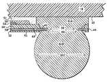
- FIG. 7depicts module 10 as lower (or level one) CSP 18 , upper (or level two) CSP 16 , 3 rd (or level three) CSP 14 , and 4 th (or level four) CSP 12 .
- some embodimentswill present HT contacts that have minimal heights that do not cause appreciable separation between the flex circuitry associated with CSP 52 and CSP 54 , for example, or between CSP 54 and CSP 58 , for example.
- the apparent height for illustrated HT joints 39particularly, that lie between respective layers of flex circuitry will be understood to be exaggerated in the depiction of FIG. 7 .
- Three sets of flex circuitry pairs 30 and 32are also shown but, as in other embodiments, the invention may be implemented with a variety of substrates including single flex circuits in place of the depicted pair and with flexible circuits that have one or plural conductive layers.
- the HT jointsprovide connections between integrated circuit devices and substrates and the overall profile of module 10 is reduced by use of the present invention that provides advantages in subsequent processing steps such as, for example, affixation of module 10 to DIMM boards, for example.
- CSP contacts 29that typically exhibit a residual layer of solder.
- a high temperature solder paste composed from a lead alloy or mixture that has a preferable melting point equal to or higher than 235° C. and preferably less than 312° C.is applied to substrate contacts 25 of a substrate such as a flexible circuit and/or the substrate contacts to which it is to be mounted.
- the CSPis positioned to place the CSP pads 29 and substrate contacts 25 in appropriate proximity. Heat is applied sufficient to melt the lead solder alloy of solder paste 27 thus forming HT joints 39 .
- the flexible circuitis positioned to place portions of the flexible circuit connector between the first CSP and a second CSP that is connected to the substrate with HT joints created using the process described for creating HT joints.
- the present inventionwill provide a stacked high module that is assembled using the HT joints that exhibit melting point ranges between X and Y degrees where X is less than Y. Attachment of the stacked module to a board is then implemented with a solder having a melting point between A and B degrees where A and B are less than X.
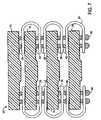
- FIG. 8is an elevation view of module 10 devised in accordance with a preferred embodiment of the present invention.
- Exemplar module 10is comprised of four CSPs: level four CSP 12 , level three CSP 14 , level two CSP 16 , and level one CSP 18 .
- Each of the depicted CSPshas an upper surface 20 and a lower surface 22 and opposite lateral sides or edges 24 and 26 and include at least one integrated circuit surrounded by a body 27 .
- Low profile contacts 28are shown in FIG. 8 .
- Low profile contacts 28provide connection to the integrated circuit or circuits within the respective packages.
- CSPsoften exhibit an array of balls along lower surface 22 .
- Such ball contactsare typically solder ball-like structures appended to contact pads arrayed along lower surface 22 .
- CSPs that exhibit balls along lower surface 22are processed to strip the balls from lower surface 22 or, alternatively, CSPs that do not have ball contacts or other contacts of appreciable height are employed. Only as a further example of the variety of contacts that may be employed in alternative preferred embodiments of the present invention, an embodiment is later disclosed in FIG. 11 and the accompanying text that is constructed using a CSP that exhibits ball contacts along lower surface 22 . The ball contacts are then reflowed to create what will be called a consolidated contact.
- Embodiments of the inventionmay also be devised that employ both standard ball contacts and low profile contacts or consolidated contacts.
- standard ball contactsmay be employed at some levels of module 10 , while low profile contacts and/or low profile inter-flex contacts or consolidated contacts are used at other levels.
- a typical eutectic ball found on a typical CSP memory deviceis approximately 15 mils in height. After solder reflow, such a ball contact will typically have a height of about 10 mils.
- low profile contacts 28 and/or low profile inter-flex contacts 42have a height of approximately 7 mils or less and, more preferably, less than 5 mils.
- the contact sites of a CSPthat are typically found under or within the ball contacts typically provided on a CSP, participate in the creation of low profile contacts 28 .
- more typical solders, in paste form for examplemay be applied either to the exposed contact sites or pads along lower surface 22 of a CSP and/or to the appropriate flex contact sites of the designated flex circuit to be employed with that CSP.
- flex circuits(“flex”, “flex circuits,” “flexible circuit structures,” “flexible circuitry”) 30 and 32 are shown connecting various constituent CSPs.
- Any flexible or conformable substrate with an internal layer connectivity capabilitymay be used as a preferable flex circuit in the invention.
- the entire flex circuitmay be flexible or, as those of skill in the art will recognize, a PCB structure made flexible in certain areas to allow conformability around CSPs and rigid in other areas for planarity along CSP surfaces may be employed as an alternative flex circuit in the present invention.
- structures known as rigid-flexmay be employed.
- Form standard 34is shown disposed adjacent to upper surface 20 of each of the CSPs below level four CSP 12 .
- Form standard 34may be fixed to upper surface 20 of the respective CSP with an adhesive 36 which preferably is thermally conductive.
- Form standard 34may also, in alternative embodiments, merely lay on upper surface 20 or be separated from upper surface 20 by an air gap or medium such as a thermal slug or non-thermal layer.
- a heat spreadermay act as a heat transference media and reside between the flex circuitry and the package body 27 or may be used in place of form standard 34 .
- a heat spreaderis shown in FIG. 14 as an example and is identified by reference numeral 37 .
- form standard 34is, in a preferred embodiment, devised from copper to create, as shown in the depicted preferred embodiment of FIG. 8 , a mandrel that mitigates thermal accumulation while providing a standard-sized form about which flex circuitry is disposed.
- Form standard 34may take other shapes and forms such as, for example, an angular “cap” that rests upon the respective CSP body.
- Form standard 34also need not be thermally enhancing although such attributes are preferable.
- the form standard 34allows modules 10 to be devised with CSPs of varying sizes, while articulating a single set of connective structures useable with the varying sizes of CSPs.
- a single set of connective structuressuch as flex circuits 30 and 32 (or a single flexible circuit in the mode where a single flex is used in place of the flex circuit pair 30 and 32 ) may be devised and used with the form standard 34 method and/or systems disclosed herein to create stacked modules from CSPs having different sized packages.
- Thiswill allow the same flexible circuitry set design to be employed to create iterations of a stacked module 10 from constituent CSPs having a first arbitrary dimension X across attribute Y (where Y may be, for example, package width), as well as modules 10 from constituent CSPs having a second arbitrary dimension X prime across that same attribute Y.
- CSPs of different sizesmay be stacked into modules 10 with the same set of connective structures (i.e. flex circuitry).
- form standard 34will present a lateral extent broader than the upper major surface of the CSP over which it is disposed.
- the CSPs from one manufacturermay be aggregated into a stacked module 10 with the same flex circuitry used to aggregate CSPs from another manufacturer into a different stacked module 10 despite the CSPs from the two different manufacturers having different dimensions.
- mixed sizes of CSPsmay be implemented into the same module 10 , such as would be useful to implement embodiments of a system-on-a-stack.
- portions of flex circuits 30 and 32are fixed to form standard 34 by adhesive 35 which is preferably a tape adhesive, but may be a liquid adhesive or may be placed in discrete locations across the package.
- adhesive 35is thermally conductive.
- flex circuits 30 and 32are multi-layer flexible circuit structures that have at least two conductive layers examples of which are described herein. Other embodiments may, however, employ flex circuitry, either as one circuit or two flex circuits to connect a pair of CSPs, that have only a single conductive layer, examples of which are also shown herein.
- the conductive layers employed in flex circuitry of module 10are metal such as alloy 110 .
- the use of plural conductive layersprovides advantages and the creation of a distributed capacitance across module 10 intended to reduce noise or bounce effects that can, particularly at higher frequencies, degrade signal integrity, as those of skill in the art will recognize.
- Module 10 of FIG. 8has plural module contacts 38 collectively identified as module array 40 .
- Connections between flex circuitsare shown as being implemented with low profile inter-flex contacts 42 which are, in preferred embodiments, low profile contacts comprised of solder-combined with pads and/or rings such as the flex contacts 44 shown in FIG. 10 or flex contacts 44 with orifices as shown in FIG. 11 being just examples.
- Form standard 34is approximately 5 mils in thickness, while flex circuits 30 and 32 are typically thinner than 5 mils. Thus, the depiction of FIG. 8 is not to scale.
- FIG. 9illustrates an exemplar two-high module 10 devised in accordance with a preferred embodiment of the present invention.
- the depiction of FIG. 9identifies two areas “A” and “B”, respectively, that are shown in greater detail in later figures.
- FIGS. 10 and 11there are shown details of two alternative embodiments for the area marked “A” in FIG. 9 .
- FIG. 12depicts details of the area marked “B” in FIG. 9 .
- FIG. 10depicts, in enlarged view, one alternative for structures that may be used in the area marked “A” in FIG. 9 .
- FIG. 10depicts an example preferred connection between an example low profile contact 28 and module contact 38 through flex contact 44 of flex 32 to illustrate a solid metal path from level one CSP 18 to module contact 38 and, therefore, to an application PWB or memory expansion board to which module 10 is connectable.
- Flex 32is shown in FIG. 10 to be comprised of multiple conductive layers. This is merely an exemplar flexible circuitry that may be employed with the present invention. A single conductive layer and other variations on the flexible circuitry may, as those of skill will recognize, be employed to advantage in alternative embodiments of the present invention.
- Flex 32has a first outer surface 50 and a second outer surface 52 .
- Preferred flex circuit 32has at least two conductive layers interior to first and second outer surfaces 50 and 52 .
- first conductive layer 54 and second conductive layer 58are interior to first and second outer surfaces 50 and 52 .
- Intermediate layer 56lies between first conductive layer 54 and second conductive layer 58 .
- the designation “F” as shown in FIG. 10notes the thickness “F” of flex circuit 32 which, in preferred embodiment, is approximately 3 mils. Thinner flex circuits may be employed, particularly where only one conductive layer is employed, and flex circuits thicker than 3 mils may also be employed, with commensurate addition to the overall height of module 10 .
- an example flex contact 44is comprised from metal at the level of second conductive layer 58 interior to second outer surface 52 .
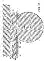
- FIG. 11depicts an alternative structure for the connection in the area marked “A” in FIG. 9 .
- a flex contact 44is penetrated by orifice 59 which has a median opening of dimension “DO” indicated by the arrow in FIG. 11 .
- Demarcation gap 63is shown in FIG. 11 . This gap may be employed to separate or demarcate flex contacts such as flex contact 44 from its respective conductive layer.
- an optional adhesive or conformed material 51 between flex circuit 32 and CSP 18is also shown in FIG. 11 .
- the consolidated contact 61 shown in FIG. 11provides connection to CSP 18 and passes through orifice 59 .
- Consolidated contact 61may be understood to have two portions 61 A that may be identified as an “inner” flex portion and, 61 B that may be identified as an “outer” flex portion, the inner and outer flex portions of consolidated contact 61 being delineated by the orifice.
- the outer flex portion 61 B of consolidated contact 61has a median lateral extent identified in FIG. 11 as “DCC” which is greater than the median opening “DO” of orifice 59 .
- the depicted consolidated contact 61is preferably created in a preferred embodiment, by providing a CSP with ball contacts.
- Those ball contactsare placed adjacent to flex contacts 44 that have orifices 59 . Heat sufficient to melt the ball contacts is applied. This causes the ball contacts to melt and reflow in part through the respective orifices 59 to create emergent from the orifices, outer flex portion 61 B, leaving inner flex portion 61 A nearer to lower surface 22 of CSP 18 .
- module 10is constructed with a level one CSP 18 that exhibits balls as contacts, but those ball contacts are re-melted during the construction of module 10 to allow the solder constituting the ball to pass through orifice 59 of the respective flex contact 44 to create a consolidated contact 61 that serves to connect CSP 18 and flex circuitry 32 , yet preserve a low profile aspect to module 10 while providing a contact for module 10 .
- this alternative connection strategymay be employed with any one or more of the CSPs of module 10 .
- a consolidated contact 61may be employed to take the place of a low profile contact 28 and module contact 38 in the alternative embodiments. Further, either alternatively, or in addition, a consolidated contact 61 may also be employed in the place of a low profile contact 28 and/or an inter-flex contact 42 in alternative embodiments where the conductive layer design of the flex circuitry will allow the penetration of the flex circuitry implicated by the strategy.
- FIG. 12depicts the area marked “B” in FIG. 9 .
- the depiction of FIG. 12includes approximations of certain dimensions of several elements in a preferred embodiment of module 10 . It must be understood that these are just examples relevant to some preferred embodiments, and those of skill will immediately recognize that the invention may be implemented with variations on these dimensions and with and without all the elements shown in FIG. 12 .
- Low profile contacts 28There are a variety of methods of creating low profile contacts 28 .
- One method that is effectiveis the screen application of solder paste to the exposed CSP contact pad areas of the CSP and/or to the contact sites of the flex circuitry.
- the reflowed joint height of contact 28will typically be between 0.002′′ and 0.006′′ (2 to 6 mils).
- the stencil design, the amount of solder remaining on ‘ball-removed’ CSPs, and flex planaritywill be factors that could have a significant effect on this value.
- Low profile contact 28has a height “C” which, in a preferred embodiment, is between 2 and 7 mils.
- Flex circuitry 32with one or two or more conductive layers, has a thickness “F” of about 4 mils or less in a preferred embodiment.
- Adhesive layer 35has a thickness “A 1 ” of between 1 and 1.5 mils in a preferred embodiment.
- Form standard 34has a thickness “FS” of between 4 and 6 mils in a preferred embodiment and, adhesive layer 36 has a thickness “A 2 ” of between 1 and 2 mils.
- a similar calculationcan be applied to identify the preferred distances between, for example, CSP 14 and CSP 16 in a four-high module 10 .
- the height of inter-flex contact 42 and thickness of another layer of flex circuit 32will be added to the sum to result in a preferred range of between 13 and 31 mils.
- not all of these elementswill be present, and in others, added elements will be found.
- some of the adhesivesmay be deleted, and form standard 34 may be replaced or added to with a heat spreader 37 and, in still other versions, neither a form standard 34 nor a heat spreader 37 will be found.
- the distance between lower surface 22 of CSP 16 and upper surface 20 of CSP 18 in a two-element module 10will be preferably between 4.5 and 12.5 mils and more preferably less than 11 mils. It is often desirable, but not required, to create low profile contacts 28 and low profile inter-flex contacts 42 using HT joints as previously described.
- FIG. 13depicts a plan view of a contact structure in flex 32 that may be employed to implement the consolidated contact 61 shown earlier in FIG. 11 .
- Shown in FIG. 13are two exemplar flex contacts 44 that each have an orifice 59 . It may be considered that flex contacts 44 extend further than the part visible in this view as represented by the dotted lines that extend into traces 45 .
- flex contact 44The part of flex contact 44 visible in this view is to be understood as being seen through windows in other layers of flex 32 as previously described, depending upon whether the flex contact is articulated at a first conductive layer or, if it is present in flex 32 , a second conductive layer and intermediate layer and whether the flex contact is for connection to the lower one of two CSPs or the upper one of two CSPs in a module 10 .
- FIG. 14depicts a flexible circuit connective set of flex circuits 30 and 32 that has a single conductive layer 64 . It should be understood with reference to FIG. 13 , that flex circuits 30 and 32 extend laterally further than shown and have portions which are, in the construction of module 10 , brought about and disposed above the present, heat spreader 37 , a form standard 34 (not shown), and/or upper surface 20 of CSP 18 . In this single conductive layer flex embodiment of module 10 , there are shown first and second outer layers 50 and 52 and intermediate layer 56 .
- Heat spreader 37is shown attached to the body 27 of first level CSP 18 through adhesive 36 .
- a heat spreader 37 or a form standard 34may also be positioned to directly contact body 27 of the respective CSP.
- Heat transference from modulecan be improved with use of a form standard 34 or a heat spreader 37 comprised of heat transference material such as a metal and preferably, copper or a copper compound or alloy, to provide a significant sink for thermal energy.
- a form standard 34 or a heat spreader 37comprised of heat transference material such as a metal and preferably, copper or a copper compound or alloy, to provide a significant sink for thermal energy.
- the flex circuitryoperates as a heat transference material, such thermal enhancement of module 10 particularly presents opportunities for improvement of thermal performance where larger numbers of CSPs are aggregated in a single stacked module 10 .
Landscapes
- Engineering & Computer Science (AREA)
- Microelectronics & Electronic Packaging (AREA)
- Power Engineering (AREA)
- Physics & Mathematics (AREA)
- Condensed Matter Physics & Semiconductors (AREA)
- General Physics & Mathematics (AREA)
- Computer Hardware Design (AREA)
- Combinations Of Printed Boards (AREA)
- Structures For Mounting Electric Components On Printed Circuit Boards (AREA)
- Production Of Multi-Layered Print Wiring Board (AREA)
- Wire Bonding (AREA)
Abstract
Description
(C+F+A1+FS+A2)−distance
Claims (6)
Priority Applications (9)
| Application Number | Priority Date | Filing Date | Title |
|---|---|---|---|
| US10/873,847US7094632B2 (en) | 2001-10-26 | 2004-06-22 | Low profile chip scale stacking system and method |
| US11/263,627US7656678B2 (en) | 2001-10-26 | 2005-10-31 | Stacked module systems |
| US11/403,081US20060255446A1 (en) | 2001-10-26 | 2006-04-12 | Stacked modules and method |
| US11/432,206US20080211077A1 (en) | 2001-10-26 | 2006-05-11 | Low profile chip scale stacking system and method |
| US11/873,355US20080120831A1 (en) | 2001-10-26 | 2007-10-16 | Stacked Modules and Method |
| US11/873,351US7719098B2 (en) | 2001-10-26 | 2007-10-16 | Stacked modules and method |
| US11/874,775US20080090329A1 (en) | 2001-10-26 | 2007-10-18 | Stacked Modules and Method |
| US11/874,795US20080088032A1 (en) | 2001-10-26 | 2007-10-18 | Stacked Modules and Method |
| US12/437,340US20090273069A1 (en) | 2001-10-26 | 2009-05-07 | Low profile chip scale stacking system and method |
Applications Claiming Priority (5)
| Application Number | Priority Date | Filing Date | Title |
|---|---|---|---|
| US10/005,581US6576992B1 (en) | 2001-10-26 | 2001-10-26 | Chip scale stacking system and method |
| US10/453,398US6914324B2 (en) | 2001-10-26 | 2003-06-03 | Memory expansion and chip scale stacking system and method |
| US10/457,608US20030234443A1 (en) | 2001-10-26 | 2003-06-09 | Low profile stacking system and method |
| US10/631,886US7026708B2 (en) | 2001-10-26 | 2003-07-14 | Low profile chip scale stacking system and method |
| US10/873,847US7094632B2 (en) | 2001-10-26 | 2004-06-22 | Low profile chip scale stacking system and method |
Related Parent Applications (2)
| Application Number | Title | Priority Date | Filing Date |
|---|---|---|---|
| US10/631,886Continuation-In-PartUS7026708B2 (en) | 2001-10-26 | 2003-07-14 | Low profile chip scale stacking system and method |
| US10/631,886ContinuationUS7026708B2 (en) | 2001-10-26 | 2003-07-14 | Low profile chip scale stacking system and method |
Related Child Applications (2)
| Application Number | Title | Priority Date | Filing Date |
|---|---|---|---|
| US11/263,627Continuation-In-PartUS7656678B2 (en) | 2001-10-26 | 2005-10-31 | Stacked module systems |
| US11/432,206ContinuationUS20080211077A1 (en) | 2001-10-26 | 2006-05-11 | Low profile chip scale stacking system and method |
Publications (2)
| Publication Number | Publication Date |
|---|---|
| US20040229402A1 US20040229402A1 (en) | 2004-11-18 |
| US7094632B2true US7094632B2 (en) | 2006-08-22 |
Family
ID=33555078
Family Applications (4)
| Application Number | Title | Priority Date | Filing Date |
|---|---|---|---|
| US10/631,886Expired - Fee RelatedUS7026708B2 (en) | 2001-10-26 | 2003-07-14 | Low profile chip scale stacking system and method |
| US10/873,847Expired - LifetimeUS7094632B2 (en) | 2001-10-26 | 2004-06-22 | Low profile chip scale stacking system and method |
| US11/432,206AbandonedUS20080211077A1 (en) | 2001-10-26 | 2006-05-11 | Low profile chip scale stacking system and method |
| US12/437,340AbandonedUS20090273069A1 (en) | 2001-10-26 | 2009-05-07 | Low profile chip scale stacking system and method |
Family Applications Before (1)
| Application Number | Title | Priority Date | Filing Date |
|---|---|---|---|
| US10/631,886Expired - Fee RelatedUS7026708B2 (en) | 2001-10-26 | 2003-07-14 | Low profile chip scale stacking system and method |
Family Applications After (2)
| Application Number | Title | Priority Date | Filing Date |
|---|---|---|---|
| US11/432,206AbandonedUS20080211077A1 (en) | 2001-10-26 | 2006-05-11 | Low profile chip scale stacking system and method |
| US12/437,340AbandonedUS20090273069A1 (en) | 2001-10-26 | 2009-05-07 | Low profile chip scale stacking system and method |
Country Status (2)
| Country | Link |
|---|---|
| US (4) | US7026708B2 (en) |
| WO (1) | WO2004112128A2 (en) |
Cited By (24)
| Publication number | Priority date | Publication date | Assignee | Title |
|---|---|---|---|---|
| US20050280134A1 (en)* | 2004-06-18 | 2005-12-22 | Tessera, Inc. | Multi-frequency noise suppression capacitor set |
| US20060049512A1 (en)* | 2004-09-03 | 2006-03-09 | Staktek Group L.P. | Thin module system and method with skew reduction |
| US20060090102A1 (en)* | 2004-09-03 | 2006-04-27 | Wehrly James D Jr | Circuit module with thermal casing systems and methods |
| US20060091529A1 (en)* | 2004-09-03 | 2006-05-04 | Staktek Group L.P. | High capacity thin module system and method |
| US20060129888A1 (en)* | 2004-09-03 | 2006-06-15 | Staktek Group L.P. | Circuit module turbulence enhacement systems and methods |
| US20060255459A1 (en)* | 2005-05-11 | 2006-11-16 | Simon Muff | Stacked semiconductor memory device |
| US7289327B2 (en) | 2006-02-27 | 2007-10-30 | Stakick Group L.P. | Active cooling methods and apparatus for modules |
| US7324352B2 (en) | 2004-09-03 | 2008-01-29 | Staktek Group L.P. | High capacity thin module system and method |
| US20080048309A1 (en)* | 2006-08-28 | 2008-02-28 | Corisis David J | Metal core foldover package structures, systems including same and methods of fabrication |
| US7423885B2 (en) | 2004-09-03 | 2008-09-09 | Entorian Technologies, Lp | Die module system |
| US7442050B1 (en) | 2005-08-29 | 2008-10-28 | Netlist, Inc. | Circuit card with flexible connection for memory module with heat spreader |
| US7468893B2 (en) | 2004-09-03 | 2008-12-23 | Entorian Technologies, Lp | Thin module system and method |
| US20080316712A1 (en)* | 2004-04-09 | 2008-12-25 | Pauley Robert S | High density module having at least two substrates and at least one thermally conductive layer therebetween |
| US7480152B2 (en) | 2004-09-03 | 2009-01-20 | Entorian Technologies, Lp | Thin module system and method |
| US7511969B2 (en) | 2006-02-02 | 2009-03-31 | Entorian Technologies, Lp | Composite core circuit module system and method |
| US7522421B2 (en) | 2004-09-03 | 2009-04-21 | Entorian Technologies, Lp | Split core circuit module |
| US7542297B2 (en) | 2004-09-03 | 2009-06-02 | Entorian Technologies, Lp | Optimized mounting area circuit module system and method |
| US7606049B2 (en) | 2004-09-03 | 2009-10-20 | Entorian Technologies, Lp | Module thermal management system and method |
| US7606040B2 (en) | 2004-09-03 | 2009-10-20 | Entorian Technologies, Lp | Memory module system and method |
| US7606050B2 (en) | 2004-09-03 | 2009-10-20 | Entorian Technologies, Lp | Compact module system and method |
| US7616452B2 (en) | 2004-09-03 | 2009-11-10 | Entorian Technologies, Lp | Flex circuit constructions for high capacity circuit module systems and methods |
| US7619893B1 (en) | 2006-02-17 | 2009-11-17 | Netlist, Inc. | Heat spreader for electronic modules |
| US7760513B2 (en) | 2004-09-03 | 2010-07-20 | Entorian Technologies Lp | Modified core for circuit module system and method |
| US8018723B1 (en) | 2008-04-30 | 2011-09-13 | Netlist, Inc. | Heat dissipation for electronic modules |
Families Citing this family (42)
| Publication number | Priority date | Publication date | Assignee | Title |
|---|---|---|---|---|
| US20050150813A1 (en)* | 2003-10-29 | 2005-07-14 | Tessera, Inc. | Foldover packages and manufacturing and test methods therefor |
| US20080203552A1 (en)* | 2005-02-15 | 2008-08-28 | Unisemicon Co., Ltd. | Stacked Package and Method of Fabricating the Same |
| US9171585B2 (en) | 2005-06-24 | 2015-10-27 | Google Inc. | Configurable memory circuit system and method |
| US8327104B2 (en) | 2006-07-31 | 2012-12-04 | Google Inc. | Adjusting the timing of signals associated with a memory system |
| US8077535B2 (en) | 2006-07-31 | 2011-12-13 | Google Inc. | Memory refresh apparatus and method |
| US8090897B2 (en) | 2006-07-31 | 2012-01-03 | Google Inc. | System and method for simulating an aspect of a memory circuit |
| US8041881B2 (en) | 2006-07-31 | 2011-10-18 | Google Inc. | Memory device with emulated characteristics |
| US8089795B2 (en) | 2006-02-09 | 2012-01-03 | Google Inc. | Memory module with memory stack and interface with enhanced capabilities |
| US20080082763A1 (en) | 2006-10-02 | 2008-04-03 | Metaram, Inc. | Apparatus and method for power management of memory circuits by a system or component thereof |
| US8060774B2 (en) | 2005-06-24 | 2011-11-15 | Google Inc. | Memory systems and memory modules |
| US20080028136A1 (en) | 2006-07-31 | 2008-01-31 | Schakel Keith R | Method and apparatus for refresh management of memory modules |
| US8796830B1 (en) | 2006-09-01 | 2014-08-05 | Google Inc. | Stackable low-profile lead frame package |
| US7386656B2 (en) | 2006-07-31 | 2008-06-10 | Metaram, Inc. | Interface circuit system and method for performing power management operations in conjunction with only a portion of a memory circuit |
| US8111566B1 (en) | 2007-11-16 | 2012-02-07 | Google, Inc. | Optimal channel design for memory devices for providing a high-speed memory interface |
| US8244971B2 (en) | 2006-07-31 | 2012-08-14 | Google Inc. | Memory circuit system and method |
| KR101377305B1 (en)* | 2005-06-24 | 2014-03-25 | 구글 인코포레이티드 | An integrated memory core and memory interface circuit |
| US8438328B2 (en) | 2008-02-21 | 2013-05-07 | Google Inc. | Emulation of abstracted DIMMs using abstracted DRAMs |
| US8335894B1 (en) | 2008-07-25 | 2012-12-18 | Google Inc. | Configurable memory system with interface circuit |
| US9542352B2 (en) | 2006-02-09 | 2017-01-10 | Google Inc. | System and method for reducing command scheduling constraints of memory circuits |
| US8130560B1 (en) | 2006-11-13 | 2012-03-06 | Google Inc. | Multi-rank partial width memory modules |
| US10013371B2 (en) | 2005-06-24 | 2018-07-03 | Google Llc | Configurable memory circuit system and method |
| US8397013B1 (en) | 2006-10-05 | 2013-03-12 | Google Inc. | Hybrid memory module |
| US8386722B1 (en) | 2008-06-23 | 2013-02-26 | Google Inc. | Stacked DIMM memory interface |
| US9507739B2 (en) | 2005-06-24 | 2016-11-29 | Google Inc. | Configurable memory circuit system and method |
| US8081474B1 (en) | 2007-12-18 | 2011-12-20 | Google Inc. | Embossed heat spreader |
| US8359187B2 (en) | 2005-06-24 | 2013-01-22 | Google Inc. | Simulating a different number of memory circuit devices |
| US8055833B2 (en) | 2006-10-05 | 2011-11-08 | Google Inc. | System and method for increasing capacity, performance, and flexibility of flash storage |
| US7609567B2 (en) | 2005-06-24 | 2009-10-27 | Metaram, Inc. | System and method for simulating an aspect of a memory circuit |
| WO2007028109A2 (en) | 2005-09-02 | 2007-03-08 | Metaram, Inc. | Methods and apparatus of stacking drams |
| US9632929B2 (en) | 2006-02-09 | 2017-04-25 | Google Inc. | Translating an address associated with a command communicated between a system and memory circuits |
| US7714453B2 (en)* | 2006-05-12 | 2010-05-11 | Broadcom Corporation | Interconnect structure and formation for package stacking of molded plastic area array package |
| US8581381B2 (en)* | 2006-06-20 | 2013-11-12 | Broadcom Corporation | Integrated circuit (IC) package stacking and IC packages formed by same |
| US7724589B2 (en) | 2006-07-31 | 2010-05-25 | Google Inc. | System and method for delaying a signal communicated from a system to at least one of a plurality of memory circuits |
| US7888185B2 (en)* | 2006-08-17 | 2011-02-15 | Micron Technology, Inc. | Semiconductor device assemblies and systems including at least one conductive pathway extending around a side of at least one semiconductor device |
| US8209479B2 (en) | 2007-07-18 | 2012-06-26 | Google Inc. | Memory circuit system and method |
| US8080874B1 (en) | 2007-09-14 | 2011-12-20 | Google Inc. | Providing additional space between an integrated circuit and a circuit board for positioning a component therebetween |
| DE202010017690U1 (en) | 2009-06-09 | 2012-05-29 | Google, Inc. | Programming dimming terminating resistor values |
| JP2011035345A (en)* | 2009-08-06 | 2011-02-17 | Fujitsu Ltd | Semiconductor device module, electronic circuit unit, electronic device, and method of manufacturing semiconductor device module |
| KR20130016682A (en)* | 2011-08-08 | 2013-02-18 | 에스케이하이닉스 주식회사 | Semiconductor chip having the structure of dual layer, packages having the same, and method of fabricating the semiconductor chip and package |
| CN111093316B (en)* | 2018-10-24 | 2021-08-24 | 鹏鼎控股(深圳)股份有限公司 | Circuit board and manufacturing method thereof |
| US11201096B2 (en)* | 2019-07-09 | 2021-12-14 | Texas Instruments Incorporated | Packaged device with die wrapped by a substrate |
| WO2022153819A1 (en)* | 2021-01-18 | 2022-07-21 | ソニーグループ株式会社 | Multilayer electronic substrate |
Citations (260)
| Publication number | Priority date | Publication date | Assignee | Title |
|---|---|---|---|---|
| US3411122A (en) | 1966-01-13 | 1968-11-12 | Ibm | Electrical resistance element and method of fabricating |
| US3436604A (en) | 1966-04-25 | 1969-04-01 | Texas Instruments Inc | Complex integrated circuit array and method for fabricating same |
| US3654394A (en) | 1969-07-08 | 1972-04-04 | Gordon Eng Co | Field effect transistor switch, particularly for multiplexing |
| US3727064A (en) | 1971-03-17 | 1973-04-10 | Monsanto Co | Opto-isolator devices and method for the fabrication thereof |
| US3746934A (en) | 1971-05-06 | 1973-07-17 | Siemens Ag | Stack arrangement of semiconductor chips |
| US3766439A (en) | 1972-01-12 | 1973-10-16 | Gen Electric | Electronic module using flexible printed circuit board with heat sink means |
| US3772776A (en) | 1969-12-03 | 1973-11-20 | Thomas & Betts Corp | Method of interconnecting memory plane boards |
| US3983547A (en) | 1974-06-27 | 1976-09-28 | International Business Machines - Ibm | Three-dimensional bubble device |
| US4079511A (en) | 1976-07-30 | 1978-03-21 | Amp Incorporated | Method for packaging hermetically sealed integrated circuit chips on lead frames |
| US4103318A (en) | 1977-05-06 | 1978-07-25 | Ford Motor Company | Electronic multichip module |
| US4288841A (en) | 1979-09-20 | 1981-09-08 | Bell Telephone Laboratories, Incorporated | Double cavity semiconductor chip carrier |
| US4398235A (en) | 1980-09-11 | 1983-08-09 | General Motors Corporation | Vertical integrated circuit package integration |
| US4406508A (en) | 1981-07-02 | 1983-09-27 | Thomas & Betts Corporation | Dual-in-line package assembly |
| US4437235A (en) | 1980-12-29 | 1984-03-20 | Honeywell Information Systems Inc. | Integrated circuit package |
| US4513368A (en) | 1981-05-22 | 1985-04-23 | Data General Corporation | Digital data processing system having object-based logical memory addressing and self-structuring modular memory |
| US4587596A (en) | 1984-04-09 | 1986-05-06 | Amp Incorporated | High density mother/daughter circuit board connector |
| US4645944A (en) | 1983-09-05 | 1987-02-24 | Matsushita Electric Industrial Co., Ltd. | MOS register for selecting among various data inputs |
| US4696525A (en) | 1985-12-13 | 1987-09-29 | Amp Incorporated | Socket for stacking integrated circuit packages |
| US4712129A (en) | 1983-12-12 | 1987-12-08 | Texas Instruments Incorporated | Integrated circuit device with textured bar cover |
| US4722691A (en) | 1986-02-03 | 1988-02-02 | General Motors Corporation | Header assembly for a printed circuit board |
| US4733461A (en) | 1984-12-28 | 1988-03-29 | Micro Co., Ltd. | Method of stacking printed circuit boards |
| US4758875A (en) | 1981-04-30 | 1988-07-19 | Hitachi, Ltd. | Resin encapsulated semiconductor device |
| US4763188A (en) | 1986-08-08 | 1988-08-09 | Thomas Johnson | Packaging system for multiple semiconductor devices |
| US4821007A (en) | 1987-02-06 | 1989-04-11 | Tektronix, Inc. | Strip line circuit component and method of manufacture |
| US4823234A (en) | 1985-08-16 | 1989-04-18 | Dai-Ichi Seiko Co., Ltd. | Semiconductor device and its manufacture |
| US4833568A (en) | 1988-01-29 | 1989-05-23 | Berhold G Mark | Three-dimensional circuit component assembly and method corresponding thereto |
| US4839717A (en) | 1986-12-19 | 1989-06-13 | Fairchild Semiconductor Corporation | Ceramic package for high frequency semiconductor devices |
| US4862249A (en) | 1987-04-17 | 1989-08-29 | Xoc Devices, Inc. | Packaging system for stacking integrated circuits |
| US4884237A (en) | 1984-03-28 | 1989-11-28 | International Business Machines Corporation | Stacked double density memory module using industry standard memory chips |
| US4891789A (en) | 1988-03-03 | 1990-01-02 | Bull Hn Information Systems, Inc. | Surface mounted multilayer memory printed circuit board |
| US4911643A (en) | 1988-10-11 | 1990-03-27 | Beta Phase, Inc. | High density and high signal integrity connector |
| US4953060A (en) | 1989-05-05 | 1990-08-28 | Ncr Corporation | Stackable integrated circuit chip package with improved heat removal |
| US4956694A (en) | 1988-11-04 | 1990-09-11 | Dense-Pac Microsystems, Inc. | Integrated circuit chip stacking |
| US4983533A (en) | 1987-10-28 | 1991-01-08 | Irvine Sensors Corporation | High-density electronic modules - process and product |
| US4985703A (en) | 1988-02-03 | 1991-01-15 | Nec Corporation | Analog multiplexer |
| US5012323A (en) | 1989-11-20 | 1991-04-30 | Micron Technology, Inc. | Double-die semiconductor package having a back-bonded die and a face-bonded die interconnected on a single leadframe |
| US5016138A (en) | 1987-10-27 | 1991-05-14 | Woodman John K | Three dimensional integrated circuit package |
| US5034350A (en) | 1987-09-23 | 1991-07-23 | Sgs Thomson Microelectronics S.R.L. | Semiconductor device package with dies mounted on both sides of the central pad of a metal frame |
| US5041902A (en) | 1989-12-14 | 1991-08-20 | Motorola, Inc. | Molded electronic package with compression structures |
| US5041015A (en) | 1990-03-30 | 1991-08-20 | Cal Flex, Inc. | Electrical jumper assembly |
| US5057903A (en) | 1989-07-17 | 1991-10-15 | Microelectronics And Computer Technology Corporation | Thermal heat sink encapsulated integrated circuit |
| US5064782A (en) | 1989-04-17 | 1991-11-12 | Sumitomo Electric Industries, Ltd. | Method of adhesively and hermetically sealing a semiconductor package lid by scrubbing |
| US5068708A (en) | 1989-10-02 | 1991-11-26 | Advanced Micro Devices, Inc. | Ground plane for plastic encapsulated integrated circuit die packages |
| US5081067A (en) | 1989-02-10 | 1992-01-14 | Fujitsu Limited | Ceramic package type semiconductor device and method of assembling the same |
| US5099393A (en) | 1991-03-25 | 1992-03-24 | International Business Machines Corporation | Electronic package for high density applications |
| US5104820A (en) | 1989-07-07 | 1992-04-14 | Irvine Sensors Corporation | Method of fabricating electronic circuitry unit containing stacked IC layers having lead rerouting |
| US5117282A (en) | 1990-10-29 | 1992-05-26 | Harris Corporation | Stacked configuration for integrated circuit devices |
| US5122862A (en) | 1989-03-15 | 1992-06-16 | Ngk Insulators, Ltd. | Ceramic lid for sealing semiconductor element and method of manufacturing the same |
| US5138434A (en) | 1991-01-22 | 1992-08-11 | Micron Technology, Inc. | Packaging for semiconductor logic devices |
| US5138430A (en) | 1991-06-06 | 1992-08-11 | International Business Machines Corporation | High performance versatile thermally enhanced IC chip mounting |
| US5159434A (en) | 1990-02-01 | 1992-10-27 | Hitachi, Ltd. | Semiconductor device having a particular chip pad structure |
| US5158912A (en) | 1991-04-09 | 1992-10-27 | Digital Equipment Corporation | Integral heatsink semiconductor package |
| US5159535A (en) | 1987-03-11 | 1992-10-27 | International Business Machines Corporation | Method and apparatus for mounting a flexible film semiconductor chip carrier on a circuitized substrate |
| US5168926A (en) | 1991-09-25 | 1992-12-08 | Intel Corporation | Heat sink design integrating interface material |
| US5198888A (en) | 1987-12-28 | 1993-03-30 | Hitachi, Ltd. | Semiconductor stacked device |
| US5198965A (en) | 1991-12-18 | 1993-03-30 | International Business Machines Corporation | Free form packaging of specific functions within a computer system |
| US5214307A (en) | 1991-07-08 | 1993-05-25 | Micron Technology, Inc. | Lead frame for semiconductor devices having improved adhesive bond line control |
| US5219794A (en) | 1991-03-14 | 1993-06-15 | Hitachi, Ltd. | Semiconductor integrated circuit device and method of fabricating same |
| US5222014A (en) | 1992-03-02 | 1993-06-22 | Motorola, Inc. | Three-dimensional multi-chip pad array carrier |
| US5224023A (en) | 1992-02-10 | 1993-06-29 | Smith Gary W | Foldable electronic assembly module |
| US5229916A (en)* | 1992-03-04 | 1993-07-20 | International Business Machines Corporation | Chip edge interconnect overlay element |
| US5239198A (en) | 1989-09-06 | 1993-08-24 | Motorola, Inc. | Overmolded semiconductor device having solder ball and edge lead connective structure |
| US5240588A (en) | 1991-08-27 | 1993-08-31 | Nec Corporation | Method for electroplating the lead pins of a semiconductor device pin grid array package |
| US5241454A (en) | 1992-01-22 | 1993-08-31 | International Business Machines Corporation | Mutlilayered flexible circuit package |
| US5243133A (en) | 1992-02-18 | 1993-09-07 | International Business Machines, Inc. | Ceramic chip carrier with lead frame or edge clip |
| US5247423A (en) | 1992-05-26 | 1993-09-21 | Motorola, Inc. | Stacking three dimensional leadless multi-chip module and method for making the same |
| US5252855A (en) | 1990-10-25 | 1993-10-12 | Mitsubishi Denki Kabushiki Kaisha | Lead frame having an anodic oxide film coating |
| US5252857A (en) | 1991-08-05 | 1993-10-12 | International Business Machines Corporation | Stacked DCA memory chips |
| US5261068A (en) | 1990-05-25 | 1993-11-09 | Dell Usa L.P. | Dual path memory retrieval system for an interleaved dynamic RAM memory unit |
| US5259770A (en) | 1992-03-19 | 1993-11-09 | Amp Incorporated | Impedance controlled elastomeric connector |
| US5262927A (en) | 1992-02-07 | 1993-11-16 | Lsi Logic Corporation | Partially-molded, PCB chip carrier package |
| US5276418A (en) | 1988-11-16 | 1994-01-04 | Motorola, Inc. | Flexible substrate electronic assembly |
| US5279029A (en) | 1990-08-01 | 1994-01-18 | Staktek Corporation | Ultra high density integrated circuit packages method |
| US5281852A (en) | 1991-12-10 | 1994-01-25 | Normington Peter J C | Semiconductor device including stacked die |
| US5289062A (en) | 1991-03-18 | 1994-02-22 | Quality Semiconductor, Inc. | Fast transmission gate switch |
| US5311401A (en) | 1991-07-09 | 1994-05-10 | Hughes Aircraft Company | Stacked chip assembly and manufacturing method therefor |
| US5313097A (en) | 1992-11-16 | 1994-05-17 | International Business Machines, Corp. | High density memory module |
| US5343075A (en) | 1991-06-29 | 1994-08-30 | Sony Corporation | Composite stacked semiconductor device with contact plates |
| US5347428A (en) | 1992-12-03 | 1994-09-13 | Irvine Sensors Corporation | Module comprising IC memory stack dedicated to and structurally combined with an IC microprocessor chip |
| US5357478A (en) | 1990-10-05 | 1994-10-18 | Mitsubishi Denki Kabushiki Kaisha | Semiconductor integrated circuit device including a plurality of cell array blocks |
| US5361228A (en) | 1992-04-30 | 1994-11-01 | Fuji Photo Film Co., Ltd. | IC memory card system having a common data and address bus |
| US5375041A (en) | 1992-12-02 | 1994-12-20 | Intel Corporation | Ra-tab array bump tab tape based I.C. package |
| US5377077A (en) | 1990-08-01 | 1994-12-27 | Staktek Corporation | Ultra high density integrated circuit packages method and apparatus |
| US5386341A (en) | 1993-11-01 | 1995-01-31 | Motorola, Inc. | Flexible substrate folded in a U-shape with a rigidizer plate located in the notch of the U-shape |
| US5394010A (en) | 1991-03-13 | 1995-02-28 | Kabushiki Kaisha Toshiba | Semiconductor assembly having laminated semiconductor devices |
| US5394303A (en) | 1992-09-11 | 1995-02-28 | Kabushiki Kaisha Toshiba | Semiconductor device |
| US5397916A (en) | 1991-12-10 | 1995-03-14 | Normington; Peter J. C. | Semiconductor device including stacked die |
| US5402006A (en) | 1992-11-10 | 1995-03-28 | Texas Instruments Incorporated | Semiconductor device with enhanced adhesion between heat spreader and leads and plastic mold compound |
| US5428190A (en) | 1993-07-02 | 1995-06-27 | Sheldahl, Inc. | Rigid-flex board with anisotropic interconnect and method of manufacture |
| US5438224A (en) | 1992-04-23 | 1995-08-01 | Motorola, Inc. | Integrated circuit package having a face-to-face IC chip arrangement |
| US5446620A (en) | 1990-08-01 | 1995-08-29 | Staktek Corporation | Ultra high density integrated circuit packages |
| US5448511A (en) | 1994-06-01 | 1995-09-05 | Storage Technology Corporation | Memory stack with an integrated interconnect and mounting structure |
| US5455740A (en) | 1994-03-07 | 1995-10-03 | Staktek Corporation | Bus communication system for stacked high density integrated circuit packages |
| US5475920A (en) | 1990-08-01 | 1995-12-19 | Burns; Carmen D. | Method of assembling ultra high density integrated circuit packages |
| US5477082A (en) | 1994-01-11 | 1995-12-19 | Exponential Technology, Inc. | Bi-planar multi-chip module |
| US5484959A (en) | 1992-12-11 | 1996-01-16 | Staktek Corporation | High density lead-on-package fabrication method and apparatus |
| US5499160A (en) | 1990-08-01 | 1996-03-12 | Staktek Corporation | High density integrated circuit module with snap-on rail assemblies |
| US5502333A (en) | 1994-03-30 | 1996-03-26 | International Business Machines Corporation | Semiconductor stack structures and fabrication/sparing methods utilizing programmable spare circuit |
| US5514907A (en) | 1995-03-21 | 1996-05-07 | Simple Technology Incorporated | Apparatus for stacking semiconductor chips |
| US5523619A (en) | 1993-11-03 | 1996-06-04 | International Business Machines Corporation | High density memory structure |
| US5523695A (en) | 1994-08-26 | 1996-06-04 | Vlsi Technology, Inc. | Universal test socket for exposing the active surface of an integrated circuit in a die-down package |
| US5541812A (en) | 1995-05-22 | 1996-07-30 | Burns; Carmen D. | Bus communication system for stacked high density integrated circuit packages having an intermediate lead frame |
| US5572065A (en) | 1992-06-26 | 1996-11-05 | Staktek Corporation | Hermetically sealed ceramic integrated circuit heat dissipating package |
| US5588205A (en) | 1995-01-24 | 1996-12-31 | Staktek Corporation | Method of manufacturing a high density integrated circuit module having complex electrical interconnect rails |
| US5592364A (en) | 1995-01-24 | 1997-01-07 | Staktek Corporation | High density integrated circuit module with complex electrical interconnect rails |
| US5594275A (en) | 1993-11-18 | 1997-01-14 | Samsung Electronics Co., Ltd. | J-leaded semiconductor package having a plurality of stacked ball grid array packages |
| US5612570A (en) | 1995-04-13 | 1997-03-18 | Dense-Pac Microsystems, Inc. | Chip stack and method of making same |
| US5642055A (en)* | 1990-02-14 | 1997-06-24 | Particle Interconnect, Inc. | Electrical interconnect using particle enhanced joining of metal surfaces |
| US5644161A (en) | 1993-03-29 | 1997-07-01 | Staktek Corporation | Ultra-high density warp-resistant memory module |
| US5646446A (en) | 1995-12-22 | 1997-07-08 | Fairchild Space And Defense Corporation | Three-dimensional flexible assembly of integrated circuits |
| US5654877A (en) | 1991-08-15 | 1997-08-05 | Staktek Corporation | Lead-on-chip integrated circuit apparatus |
| US5657537A (en) | 1995-05-30 | 1997-08-19 | General Electric Company | Method for fabricating a stack of two dimensional circuit modules |
| US5677569A (en) | 1994-10-27 | 1997-10-14 | Samsung Electronics Co., Ltd. | Semiconductor multi-package stack |
| US5729894A (en) | 1992-07-21 | 1998-03-24 | Lsi Logic Corporation | Method of assembling ball bump grid array semiconductor packages |
| US5744827A (en) | 1995-11-28 | 1998-04-28 | Samsung Electronics Co., Ltd. | Three dimensional stack package device having exposed coupling lead portions and vertical interconnection elements |
| US5751553A (en) | 1992-09-16 | 1998-05-12 | Clayton; James E. | Thin multichip module including a connector frame socket having first and second apertures |
| US5764497A (en) | 1995-11-13 | 1998-06-09 | Minolta Co, Ltd. | Circuit board connection method and connection structure |
| US5763296A (en) | 1991-11-21 | 1998-06-09 | Sgs-Thomson Microelectronics S.R.L. | Method for fabricating an electronic device structure with studs locating lead frame on backing plate |
| US5778522A (en) | 1996-05-20 | 1998-07-14 | Staktek Corporation | Method of manufacturing a high density integrated circuit module with complex electrical interconnect rails having electrical interconnect strain relief |
| US5778552A (en) | 1995-05-08 | 1998-07-14 | Renishaw Plc | Touch sensor |
| US5783464A (en) | 1992-06-26 | 1998-07-21 | Staktek Corporation | Method of forming a hermetically sealed circuit lead-on package |
| US5789815A (en) | 1996-04-23 | 1998-08-04 | Motorola, Inc. | Three dimensional semiconductor package having flexible appendages |
| US5801437A (en) | 1993-03-29 | 1998-09-01 | Staktek Corporation | Three-dimensional warp-resistant integrated circuit module method and apparatus |
| US5801439A (en) | 1994-04-20 | 1998-09-01 | Fujitsu Limited | Semiconductor device and semiconductor device unit for a stack arrangement |
| US5805422A (en) | 1994-09-21 | 1998-09-08 | Nec Corporation | Semiconductor package with flexible board and method of fabricating the same |
| US5835988A (en) | 1996-03-27 | 1998-11-10 | Mitsubishi Denki Kabushiki Kaisha | Packed semiconductor device with wrap around external leads |
| US5841721A (en) | 1994-09-03 | 1998-11-24 | Samsung Electronics Co., Ltd | Multi-block erase and verification circuit in a nonvolatile semiconductor memory device and a method thereof |
| US5869353A (en) | 1997-11-17 | 1999-02-09 | Dense-Pac Microsystems, Inc. | Modular panel stacking process |
| US5895970A (en)* | 1997-05-02 | 1999-04-20 | Nec Corporation | Semiconductor package having semiconductor element, mounting structure of semiconductor package mounted on circuit board, and method of assembling semiconductor package |
| US5899705A (en) | 1997-11-20 | 1999-05-04 | Akram; Salman | Stacked leads-over chip multi-chip module |
| US5917709A (en)* | 1997-06-16 | 1999-06-29 | Eastman Kodak Company | Multiple circuit board assembly having an interconnect mechanism that includes a flex connector |
| US5922061A (en) | 1995-10-20 | 1999-07-13 | Iq Systems | Methods and apparatus for implementing high speed data communications |
| US5925934A (en) | 1995-10-28 | 1999-07-20 | Institute Of Microelectronics | Low cost and highly reliable chip-sized package |
| US5926369A (en) | 1998-01-22 | 1999-07-20 | International Business Machines Corporation | Vertically integrated multi-chip circuit package with heat-sink support |
| US5949657A (en) | 1997-12-01 | 1999-09-07 | Karabatsos; Chris | Bottom or top jumpered foldable electronic assembly |
| US5953215A (en) | 1997-12-01 | 1999-09-14 | Karabatsos; Chris | Apparatus and method for improving computer memory speed and capacity |
| US5959839A (en) | 1997-01-02 | 1999-09-28 | At&T Corp | Apparatus for heat removal using a flexible backplane |
| US5963427A (en) | 1997-12-11 | 1999-10-05 | Sun Microsystems, Inc. | Multi-chip module with flexible circuit board |
| US5973395A (en) | 1996-04-30 | 1999-10-26 | Yamaichi Electronics Co., Ltd. | IC package having a single wiring sheet with a lead pattern disposed thereon |
| US5995370A (en) | 1997-09-01 | 1999-11-30 | Sharp Kabushiki Kaisha | Heat-sinking arrangement for circuit elements |
| US6002589A (en) | 1997-07-21 | 1999-12-14 | Rambus Inc. | Integrated circuit package for coupling to a printed circuit board |
| US6002167A (en) | 1995-09-22 | 1999-12-14 | Hitachi Cable, Ltd. | Semiconductor device having lead on chip structure |
| US6014316A (en) | 1997-06-13 | 2000-01-11 | Irvine Sensors Corporation | IC stack utilizing BGA contacts |
| US6025642A (en) | 1995-08-17 | 2000-02-15 | Staktek Corporation | Ultra high density integrated circuit packages |
| US6028365A (en) | 1998-03-30 | 2000-02-22 | Micron Technology, Inc. | Integrated circuit package and method of fabrication |
| US6028352A (en) | 1997-06-13 | 2000-02-22 | Irvine Sensors Corporation | IC stack utilizing secondary leadframes |
| US6034878A (en) | 1996-12-16 | 2000-03-07 | Hitachi, Ltd. | Source-clock-synchronized memory system and memory unit |
| US6040624A (en) | 1997-10-02 | 2000-03-21 | Motorola, Inc. | Semiconductor device package and method |
| US6072233A (en) | 1998-05-04 | 2000-06-06 | Micron Technology, Inc. | Stackable ball grid array package |
| US6084294A (en) | 1998-08-26 | 2000-07-04 | Mitsubishi Denki Kabushiki Kaisha | Semiconductor device comprising stacked semiconductor elements |
| US6084293A (en) | 1997-07-25 | 2000-07-04 | Oki Electric Industry Co., Ltd. | Stacked semiconductor device |
| US6097087A (en) | 1997-10-31 | 2000-08-01 | Micron Technology, Inc. | Semiconductor package including flex circuit, interconnects and dense array external contacts |
| US6121676A (en) | 1996-12-13 | 2000-09-19 | Tessera, Inc. | Stacked microelectronic assembly and method therefor |
| US6157541A (en) | 1997-12-30 | 2000-12-05 | Siemens Aktiengesellschaft | Stack arrangement for two semiconductor memory chips and printed board for accepting a plurality of such stack arrangements |
| US6172874B1 (en) | 1998-04-06 | 2001-01-09 | Silicon Graphics, Inc. | System for stacking of integrated circuit packages |
| US6178093B1 (en) | 1996-06-28 | 2001-01-23 | International Business Machines Corporation | Information handling system with circuit assembly having holes filled with filler material |
| US6187652B1 (en) | 1998-09-14 | 2001-02-13 | Fujitsu Limited | Method of fabrication of multiple-layer high density substrate |
| US6205654B1 (en) | 1992-12-11 | 2001-03-27 | Staktek Group L.P. | Method of manufacturing a surface mount package |
| US6208521B1 (en)* | 1997-05-19 | 2001-03-27 | Nitto Denko Corporation | Film carrier and laminate type mounting structure using same |
| US6222737B1 (en) | 1999-04-23 | 2001-04-24 | Dense-Pac Microsystems, Inc. | Universal package and method of forming the same |
| US6225688B1 (en) | 1997-12-11 | 2001-05-01 | Tessera, Inc. | Stacked microelectronic assembly and method therefor |
| US6233650B1 (en) | 1998-04-01 | 2001-05-15 | Intel Corporation | Using FET switches for large memory arrays |
| US6234820B1 (en) | 1997-07-21 | 2001-05-22 | Rambus Inc. | Method and apparatus for joining printed circuit boards |
| US6262895B1 (en) | 2000-01-13 | 2001-07-17 | John A. Forthun | Stackable chip package with flex carrier |
| US6262476B1 (en) | 1998-07-27 | 2001-07-17 | Siemens Aktiengesellschaft | Composite member composed of at least two integrated circuits and method for the manufacture of a composite member composed of at least two integrated circuits |
| US6266252B1 (en) | 1997-12-01 | 2001-07-24 | Chris Karabatsos | Apparatus and method for terminating a computer memory bus |
| US6265660B1 (en) | 1997-07-09 | 2001-07-24 | Micron Technology, Inc. | Package stack via bottom leaded plastic (BLP) packaging |
| US20010013423A1 (en) | 1996-10-31 | 2001-08-16 | Hormazdyar M. Dalal | Flip chip attach on flexible circuit carrier using chip with metallic cap on solder |
| US6281577B1 (en) | 1996-06-28 | 2001-08-28 | Pac Tech-Packaging Technologies Gmbh | Chips arranged in plurality of planes and electrically connected to one another |
| US6285560B1 (en) | 1999-09-20 | 2001-09-04 | Texas Instruments Incorporated | Method for increasing device reliability by selectively depopulating solder balls from a foot print of a ball grid array (BGA) package, and device so modified |
| US6300679B1 (en)* | 1998-06-01 | 2001-10-09 | Semiconductor Components Industries, Llc | Flexible substrate for packaging a semiconductor component |
| US6303981B1 (en) | 1999-09-01 | 2001-10-16 | Micron Technology, Inc. | Semiconductor package having stacked dice and leadframes and method of fabrication |
| US6310392B1 (en) | 1998-12-28 | 2001-10-30 | Staktek Group, L.P. | Stacked micro ball grid array packages |
| US20010035572A1 (en) | 1999-05-05 | 2001-11-01 | Isaak Harlan R. | Stackable flex circuit chip package and method of making same |
| US6313998B1 (en) | 1999-04-02 | 2001-11-06 | Legacy Electronics, Inc. | Circuit board assembly having a three dimensional array of integrated circuit packages |
| US6316825B1 (en) | 1998-05-15 | 2001-11-13 | Hyundai Electronics Industries Co., Ltd. | Chip stack package utilizing a connecting hole to improve electrical connection between leadframes |
| US20010040793A1 (en)* | 2000-02-01 | 2001-11-15 | Tetsuya Inaba | Electronic device and method of producing the same |
| US6323060B1 (en) | 1999-05-05 | 2001-11-27 | Dense-Pac Microsystems, Inc. | Stackable flex circuit IC package and method of making same |
| US6329708B1 (en) | 1999-04-26 | 2001-12-11 | Oki Electric Industry Co. Ltd. | Micro ball grid array semiconductor device and semiconductor module |
| US6336262B1 (en) | 1996-10-31 | 2002-01-08 | International Business Machines Corporation | Process of forming a capacitor with multi-level interconnection technology |
| US20020006032A1 (en) | 2000-05-23 | 2002-01-17 | Chris Karabatsos | Low-profile registered DIMM |
| US20020027441A1 (en)* | 1996-04-01 | 2002-03-07 | Salman Akram | Semiconductor test interconnect with variable flexure contacts |
| US20020030995A1 (en) | 2000-08-07 | 2002-03-14 | Masao Shoji | Headlight |
| US6376769B1 (en) | 1999-05-18 | 2002-04-23 | Amerasia International Technology, Inc. | High-density electronic package, and method for making same |
| US6392162B1 (en) | 2000-11-10 | 2002-05-21 | Chris Karabatsos | Double-sided flexible jumper assembly and method of manufacture |
| US20020076919A1 (en) | 1998-11-13 | 2002-06-20 | Peters Michael G. | Composite interposer and method for producing a composite interposer |
| US6410857B1 (en)* | 2001-03-01 | 2002-06-25 | Lockheed Martin Corporation | Signal cross-over interconnect for a double-sided circuit card assembly |
| US6426560B1 (en) | 1999-08-06 | 2002-07-30 | Hitachi, Ltd. | Semiconductor device and memory module |
| US20020101261A1 (en) | 2001-02-01 | 2002-08-01 | Chris Karabatsos | Tri-directional, high-speed bus switch |
| US6433418B1 (en) | 1998-07-24 | 2002-08-13 | Fujitsu Limited | Apparatus for a vertically accumulable semiconductor device with external leads secured by a positioning mechanism |
| US6444921B1 (en) | 2000-02-03 | 2002-09-03 | Fujitsu Limited | Reduced stress and zero stress interposers for integrated-circuit chips, multichip substrates, and the like |
| US6446158B1 (en) | 1999-05-17 | 2002-09-03 | Chris Karabatsos | Memory system using FET switches to select memory banks |
| US6444490B2 (en) | 1998-06-26 | 2002-09-03 | International Business Machines Corporation | Micro-flex technology in semiconductor packages |
| US6449159B1 (en) | 2000-05-03 | 2002-09-10 | Rambus Inc. | Semiconductor module with imbedded heat spreader |
| US6452826B1 (en) | 2000-10-26 | 2002-09-17 | Samsung Electronics Co., Ltd. | Memory module system |
| US20020139577A1 (en) | 2001-03-27 | 2002-10-03 | Miller Charles A. | In-street integrated circuit wafer via |
| US6462412B2 (en) | 2000-01-18 | 2002-10-08 | Sony Corporation | Foldable, flexible laminate type semiconductor apparatus with reinforcing and heat-radiating plates |
| US6465893B1 (en) | 1990-09-24 | 2002-10-15 | Tessera, Inc. | Stacked chip assembly |
| US20020164838A1 (en) | 2001-05-02 | 2002-11-07 | Moon Ow Chee | Flexible ball grid array chip scale packages and methods of fabrication |
| US6486544B1 (en) | 1998-09-09 | 2002-11-26 | Seiko Epson Corporation | Semiconductor device and method manufacturing the same, circuit board, and electronic instrument |
| US6489687B1 (en)* | 1999-10-01 | 2002-12-03 | Seiko Epson Corporation | Semiconductor device and method of manufacturing the same, manufacturing device, circuit board, and electronic equipment |
| US6489178B2 (en) | 2000-01-26 | 2002-12-03 | Texas Instruments Incorporated | Method of fabricating a molded package for micromechanical devices |
| US20020180022A1 (en) | 1999-10-20 | 2002-12-05 | Seiko Epson Corporation | Semiconductor device |
| US6492718B2 (en) | 1999-12-20 | 2002-12-10 | Kabushiki Kaisha Toshiba | Stacked semiconductor device and semiconductor system |
| US6509639B1 (en) | 2001-07-27 | 2003-01-21 | Charles W. C. Lin | Three-dimensional stacked semiconductor package |
| US20030016710A1 (en) | 2001-07-19 | 2003-01-23 | Satoshi Komoto | Semiconductor laser device including light receiving element for receiving monitoring laser beam |
| US6528870B2 (en) | 2000-01-28 | 2003-03-04 | Kabushiki Kaisha Toshiba | Semiconductor device having a plurality of stacked wiring boards |
| US20030049886A1 (en) | 2001-09-07 | 2003-03-13 | Salmon Peter C. | Electronic system modules and method of fabrication |
| US6552910B1 (en) | 2000-06-28 | 2003-04-22 | Micron Technology, Inc. | Stacked-die assemblies with a plurality of microelectronic devices and methods of manufacture |
| US20030082845A1 (en)* | 2000-01-14 | 2003-05-01 | Amkor Technology, Inc. | Package for multiple integrated circuits and method of making |
| WO2003037053A1 (en) | 2001-10-26 | 2003-05-01 | Staktek Group, L.P. | Chip scale stacking system and method |
| US20030081392A1 (en) | 2001-10-26 | 2003-05-01 | Staktek Group, L.P. | Integrated circuit stacking system and method |
| US6560117B2 (en) | 2000-06-28 | 2003-05-06 | Micron Technology, Inc. | Packaged microelectronic die assemblies and methods of manufacture |
| US6572387B2 (en) | 1999-09-24 | 2003-06-03 | Staktek Group, L.P. | Flexible circuit connector for stacked chip module |
| US6574113B2 (en)* | 1999-03-31 | 2003-06-03 | International Business Machines Corporation | Electronic package with stacked connections and method for making same |
| US20030109078A1 (en) | 1996-12-03 | 2003-06-12 | Yoshikazu Takahashi | Semiconductor device, method for manufacturing the same, and method for mounting the same |
| US20030107118A1 (en) | 2001-10-09 | 2003-06-12 | Tessera, Inc. | Stacked packages |
| US6588095B2 (en) | 2001-04-27 | 2003-07-08 | Hewlett-Packard Development Company, Lp. | Method of processing a device by electrophoresis coating |
| US6590282B1 (en) | 2002-04-12 | 2003-07-08 | Industrial Technology Research Institute | Stacked semiconductor package formed on a substrate and method for fabrication |
| US6600222B1 (en) | 2002-07-17 | 2003-07-29 | Intel Corporation | Stacked microelectronic packages |
| US6614664B2 (en)* | 2000-10-24 | 2003-09-02 | Samsung Electronics Co., Ltd. | Memory module having series-connected printed circuit boards |
| US20030168725A1 (en) | 1996-12-13 | 2003-09-11 | Tessera, Inc. | Methods of making microelectronic assemblies including folded substrates |
| US6620651B2 (en) | 2001-10-23 | 2003-09-16 | National Starch And Chemical Investment Holding Corporation | Adhesive wafers for die attach application |
| US6627984B2 (en) | 2001-07-24 | 2003-09-30 | Dense-Pac Microsystems, Inc. | Chip stack with differing chip package types |
| US6657134B2 (en) | 2001-11-30 | 2003-12-02 | Honeywell International Inc. | Stacked ball grid array |
| US6660561B2 (en) | 2000-06-15 | 2003-12-09 | Dpac Technologies Corp. | Method of assembling a stackable integrated circuit chip |
| US6661247B2 (en)* | 1997-09-19 | 2003-12-09 | Fujitsu Limited | Semiconductor testing device |
| US20040000708A1 (en) | 2001-10-26 | 2004-01-01 | Staktek Group, L.P. | Memory expansion and chip scale stacking system and method |
| US6677670B2 (en) | 2000-04-25 | 2004-01-13 | Seiko Epson Corporation | Semiconductor device |
| US6683377B1 (en) | 2000-05-30 | 2004-01-27 | Amkor Technology, Inc. | Multi-stacked memory package |
| US20040021211A1 (en) | 2002-08-05 | 2004-02-05 | Tessera, Inc. | Microelectronic adaptors, assemblies and methods |
| US6690584B2 (en) | 2000-08-14 | 2004-02-10 | Fujitsu Limited | Information-processing device having a crossbar-board connected to back panels on different sides |
| US20040031972A1 (en) | 2001-10-09 | 2004-02-19 | Tessera, Inc. | Stacked packages |
| US20040045159A1 (en) | 1996-12-13 | 2004-03-11 | Tessera, Inc. | Electrical connection with inwardly deformable contacts |
| US6707684B1 (en) | 2001-04-02 | 2004-03-16 | Advanced Micro Devices, Inc. | Method and apparatus for direct connection between two integrated circuits via a connector |
| US6709893B2 (en)* | 1998-05-11 | 2004-03-23 | Micron Technology, Inc. | Interconnections for a semiconductor device and method for forming same |
| US20040065963A1 (en) | 2002-09-17 | 2004-04-08 | Chippac, Inc. | Semiconductor multi-package module having wire bond interconnect between stacked packages and having electrical shield |
| US20040075991A1 (en) | 1999-08-11 | 2004-04-22 | Tessera. Inc. | Vapor phase connection techniques |
| US20040099938A1 (en) | 2002-09-11 | 2004-05-27 | Tessera, Inc. | Assemblies having stacked semiconductor chips and methods of making same |
| US20040104470A1 (en) | 2002-08-16 | 2004-06-03 | Tessera, Inc. | Microelectronic packages with self-aligning features |
| US20040115866A1 (en) | 2002-09-06 | 2004-06-17 | Tessera, Inc. | Methods of making microelectronic packages including folded substrates |
| US6768660B2 (en) | 2001-01-08 | 2004-07-27 | Samsung Electronics Co. Ltd. | Multi-chip memory devices and modules including independent control of memory chips |
| US20040150107A1 (en) | 2002-12-31 | 2004-08-05 | Cha Ki Bon | Stack package and fabricating method thereof |
| US20040157352A1 (en) | 2000-11-13 | 2004-08-12 | Kim Soo Kil | Method for forming thin film and method for fabricating liquid crystal display using the same |
| US6781240B2 (en) | 2001-06-26 | 2004-08-24 | Samsung Electronics Co., Ltd. | Semiconductor package with semiconductor chips stacked therein and method of making the package |
| US6803651B1 (en) | 2002-01-09 | 2004-10-12 | Bridge Semiconductor Corporation | Optoelectronic semiconductor package device |
| US6812567B2 (en) | 2002-11-28 | 2004-11-02 | Samsung Electronics Co., Ltd. | Semiconductor package and package stack made thereof |
| US20040217471A1 (en) | 2003-02-27 | 2004-11-04 | Tessera, Inc. | Component and assemblies with ends offset downwardly |
| US20040238931A1 (en) | 2003-05-30 | 2004-12-02 | Tessera, Inc. | Assemblies having stacked semiconductor chips and methods of making same |
| US20040245617A1 (en) | 2003-05-06 | 2004-12-09 | Tessera, Inc. | Dense multichip module |
| US6833984B1 (en) | 2000-05-03 | 2004-12-21 | Rambus, Inc. | Semiconductor module with serial bus connection to multiple dies |
| US20050018495A1 (en) | 2004-01-29 | 2005-01-27 | Netlist, Inc. | Arrangement of integrated circuits in a memory module |
| US6849949B1 (en) | 1999-09-27 | 2005-02-01 | Samsung Electronics Co., Ltd. | Thin stacked package |
| US20050035440A1 (en) | 2001-08-22 | 2005-02-17 | Tessera, Inc. | Stacked chip assembly with stiffening layer |
| US20050040508A1 (en) | 2003-08-22 | 2005-02-24 | Jong-Joo Lee | Area array type package stack and manufacturing method thereof |
| US6867496B1 (en)* | 1999-10-01 | 2005-03-15 | Seiko Epson Corporation | Interconnect substrate, semiconductor device, methods of fabricating, inspecting, and mounting the semiconductor device, circuit board, and electronic instrument |
| US6876074B2 (en) | 2001-10-10 | 2005-04-05 | Samsung Electronics Co., Ltd. | Stack package using flexible double wiring substrate |
| US6884653B2 (en) | 2001-03-21 | 2005-04-26 | Micron Technology, Inc. | Folded interposer |
| US6891729B2 (en) | 2001-09-10 | 2005-05-10 | Samsung Electronics Co., Ltd. | Memory module |
| US20050133897A1 (en) | 2003-12-17 | 2005-06-23 | Baek Joong-Hyun | Stack package with improved heat radiation and module having the stack package mounted thereon |
Family Cites Families (58)
| Publication number | Priority date | Publication date | Assignee | Title |
|---|---|---|---|---|
| US3372310A (en)* | 1965-04-30 | 1968-03-05 | Radiation Inc | Universal modular packages for integrated circuits |
| US3718842A (en)* | 1972-04-21 | 1973-02-27 | Texas Instruments Inc | Liquid crystal display mounting structure |
| US3806767A (en)* | 1973-03-15 | 1974-04-23 | Tek Wave Inc | Interboard connector |
| SU834957A1 (en) | 1979-03-12 | 1981-05-30 | Предприятие П/Я А-7438 | Device for feeding printed circuit boards |
| US4381421A (en)* | 1980-07-01 | 1983-04-26 | Tektronix, Inc. | Electromagnetic shield for electronic equipment |
| US4429349A (en)* | 1980-09-30 | 1984-01-31 | Burroughs Corporation | Coil connector |
| US4420794A (en)* | 1981-09-10 | 1983-12-13 | Research, Incorporated | Integrated circuit switch |
| US4567543A (en)* | 1983-02-15 | 1986-01-28 | Motorola, Inc. | Double-sided flexible electronic circuit module |
| US4727513A (en)* | 1983-09-02 | 1988-02-23 | Wang Laboratories, Inc. | Signal in-line memory module |
| JPS60254762A (en) | 1984-05-31 | 1985-12-16 | Fujitsu Ltd | Semiconductor device package |
| US4724611A (en)* | 1985-08-23 | 1988-02-16 | Nec Corporation | Method for producing semiconductor module |
| JPS62162891U (en)* | 1986-04-03 | 1987-10-16 | ||
| KR970003915B1 (en)* | 1987-06-24 | 1997-03-22 | 미다 가쓰시게 | Semiconductor memory device and semiconductor memory module using same |
| US4992850A (en)* | 1989-02-15 | 1991-02-12 | Micron Technology, Inc. | Directly bonded simm module |
| US4992849A (en)* | 1989-02-15 | 1991-02-12 | Micron Technology, Inc. | Directly bonded board multiple integrated circuit module |
| US4967950A (en)* | 1989-10-31 | 1990-11-06 | International Business Machines Corporation | Soldering method |
| US5229641A (en)* | 1989-11-25 | 1993-07-20 | Hitachi Maxell, Ltd. | Semiconductor card and manufacturing method therefor |
| US5191404A (en)* | 1989-12-20 | 1993-03-02 | Digital Equipment Corporation | High density memory array packaging |
| US5345205A (en)* | 1990-04-05 | 1994-09-06 | General Electric Company | Compact high density interconnected microwave system |
| US5050039A (en)* | 1990-06-26 | 1991-09-17 | Digital Equipment Corporation | Multiple circuit chip mounting and cooling arrangement |
| US5852326A (en)* | 1990-09-24 | 1998-12-22 | Tessera, Inc. | Face-up semiconductor chip assembly |
| US5289346A (en)* | 1991-02-26 | 1994-02-22 | Microelectronics And Computer Technology Corporation | Peripheral to area adapter with protective bumper for an integrated circuit chip |
| US5714802A (en)* | 1991-06-18 | 1998-02-03 | Micron Technology, Inc. | High-density electronic module |
| MY109101A (en)* | 1992-05-25 | 1996-12-31 | Hitachi Ltd | Thin type semiconductor device, module structure using the device and method of mounting the device on board |
| EP0597087B1 (en)* | 1992-06-02 | 1999-07-28 | Hewlett-Packard Company | Computer-aided design method for multilevel interconnect technologies |
| US5343366A (en)* | 1992-06-24 | 1994-08-30 | International Business Machines Corporation | Packages for stacked integrated circuit chip cubes |
| US5266912A (en)* | 1992-08-19 | 1993-11-30 | Micron Technology, Inc. | Inherently impedance matched multiple integrated circuit module |
| JPH0679990A (en)* | 1992-09-04 | 1994-03-22 | Mitsubishi Electric Corp | Ic memory card |
| US5432630A (en)* | 1992-09-11 | 1995-07-11 | Motorola, Inc. | Optical bus with optical transceiver modules and method of manufacture |
| US5384690A (en)* | 1993-07-27 | 1995-01-24 | International Business Machines Corporation | Flex laminate package for a parallel processor |
| US5396573A (en)* | 1993-08-03 | 1995-03-07 | International Business Machines Corporation | Pluggable connectors for connecting large numbers of electrical and/or optical cables to a module through a seal |
| US5337388A (en)* | 1993-08-03 | 1994-08-09 | International Business Machines Corporation | Matrix of pluggable connectors for connecting large numbers of clustered electrical and/or opticcal cables to a module |
| JPH07312469A (en)* | 1994-05-16 | 1995-11-28 | Nippon Mektron Ltd | Structure of bent part of multilayer flexible circuit board |
| US5644839A (en)* | 1994-06-10 | 1997-07-08 | Xetel Corporation | Surface mountable substrate edge terminal |
| US5509197A (en)* | 1994-06-10 | 1996-04-23 | Xetel Corporation | Method of making substrate edge connector |
| US5491612A (en)* | 1995-02-21 | 1996-02-13 | Fairchild Space And Defense Corporation | Three-dimensional modular assembly of integrated circuits |
| JP2606177B2 (en)* | 1995-04-26 | 1997-04-30 | 日本電気株式会社 | Printed wiring board |
| US5872051A (en)* | 1995-08-02 | 1999-02-16 | International Business Machines Corporation | Process for transferring material to semiconductor chip conductive pads using a transfer substrate |
| JP3718008B2 (en)* | 1996-02-26 | 2005-11-16 | 株式会社日立製作所 | Memory module and manufacturing method thereof |
| US6008538A (en)* | 1996-10-08 | 1999-12-28 | Micron Technology, Inc. | Method and apparatus providing redundancy for fabricating highly reliable memory modules |
| JPH1117099A (en)* | 1996-11-12 | 1999-01-22 | T I F:Kk | Memory module |
| JPH10173122A (en)* | 1996-12-06 | 1998-06-26 | Mitsubishi Electric Corp | Memory module |
| US5933712A (en)* | 1997-03-19 | 1999-08-03 | The Regents Of The University Of California | Attachment method for stacked integrated circuit (IC) chips |
| US6021048A (en)* | 1998-02-17 | 2000-02-01 | Smith; Gary W. | High speed memory module |
| US6180881B1 (en)* | 1998-05-05 | 2001-01-30 | Harlan Ruben Isaak | Chip stack and method of making same |
| DE19941672A1 (en)* | 1998-09-09 | 2000-03-16 | Fuji Photo Film Co Ltd | Image reader for image generation system, performs control measurement using slower transport speed, or using longer image reading interval image cannot be read correctly due to density |
| US6347394B1 (en)* | 1998-11-04 | 2002-02-12 | Micron Technology, Inc. | Buffering circuit embedded in an integrated circuit device module used for buffering clocks and other input signals |
| TW511723U (en)* | 1998-12-28 | 2002-11-21 | Foxconn Prec Components Co Ltd | Memory bus module |
| US6370668B1 (en)* | 1999-07-23 | 2002-04-09 | Rambus Inc | High speed memory system capable of selectively operating in non-chip-kill and chip-kill modes |
| US6181577B1 (en)* | 1999-07-26 | 2001-01-30 | Lucent Technologies Inc. | Auxiliary bias circuit for a power supply and a method of operation thereof |
| US6265662B1 (en)* | 1999-11-05 | 2001-07-24 | The Lamson & Sessions Co. | Floor box assembly |
| JP2001223323A (en)* | 2000-02-10 | 2001-08-17 | Mitsubishi Electric Corp | Semiconductor device |
| US6349050B1 (en)* | 2000-10-10 | 2002-02-19 | Rambus, Inc. | Methods and systems for reducing heat flux in memory systems |
| DE10131939B4 (en)* | 2001-07-02 | 2014-12-11 | Qimonda Ag | Electronic circuit board with a plurality of housing-type housing semiconductor memories |
| JP2003045179A (en)* | 2001-08-01 | 2003-02-14 | Mitsubishi Electric Corp | Semiconductor element and semiconductor memory module using the same |
| JP2003059297A (en)* | 2001-08-08 | 2003-02-28 | Mitsubishi Electric Corp | Semiconductor storage device and semiconductor module using the same |
| US20030234443A1 (en)* | 2001-10-26 | 2003-12-25 | Staktek Group, L.P. | Low profile stacking system and method |
| JP2004055009A (en)* | 2002-07-18 | 2004-02-19 | Renesas Technology Corp | Semiconductor memory module |
- 2003
- 2003-07-14USUS10/631,886patent/US7026708B2/ennot_activeExpired - Fee Related
- 2004
- 2004-05-25WOPCT/US2004/016347patent/WO2004112128A2/enactiveApplication Filing
- 2004-06-22USUS10/873,847patent/US7094632B2/ennot_activeExpired - Lifetime
- 2006
- 2006-05-11USUS11/432,206patent/US20080211077A1/ennot_activeAbandoned
- 2009
- 2009-05-07USUS12/437,340patent/US20090273069A1/ennot_activeAbandoned
Patent Citations (292)
| Publication number | Priority date | Publication date | Assignee | Title |
|---|---|---|---|---|
| US3411122A (en) | 1966-01-13 | 1968-11-12 | Ibm | Electrical resistance element and method of fabricating |
| US3436604A (en) | 1966-04-25 | 1969-04-01 | Texas Instruments Inc | Complex integrated circuit array and method for fabricating same |
| US3654394A (en) | 1969-07-08 | 1972-04-04 | Gordon Eng Co | Field effect transistor switch, particularly for multiplexing |
| US3772776A (en) | 1969-12-03 | 1973-11-20 | Thomas & Betts Corp | Method of interconnecting memory plane boards |
| US3727064A (en) | 1971-03-17 | 1973-04-10 | Monsanto Co | Opto-isolator devices and method for the fabrication thereof |
| US3746934A (en) | 1971-05-06 | 1973-07-17 | Siemens Ag | Stack arrangement of semiconductor chips |
| US3766439A (en) | 1972-01-12 | 1973-10-16 | Gen Electric | Electronic module using flexible printed circuit board with heat sink means |
| US3983547A (en) | 1974-06-27 | 1976-09-28 | International Business Machines - Ibm | Three-dimensional bubble device |
| US4079511A (en) | 1976-07-30 | 1978-03-21 | Amp Incorporated | Method for packaging hermetically sealed integrated circuit chips on lead frames |
| US4103318A (en) | 1977-05-06 | 1978-07-25 | Ford Motor Company | Electronic multichip module |
| US4288841A (en) | 1979-09-20 | 1981-09-08 | Bell Telephone Laboratories, Incorporated | Double cavity semiconductor chip carrier |
| US4398235A (en) | 1980-09-11 | 1983-08-09 | General Motors Corporation | Vertical integrated circuit package integration |
| US4437235A (en) | 1980-12-29 | 1984-03-20 | Honeywell Information Systems Inc. | Integrated circuit package |
| US4758875A (en) | 1981-04-30 | 1988-07-19 | Hitachi, Ltd. | Resin encapsulated semiconductor device |
| US4513368A (en) | 1981-05-22 | 1985-04-23 | Data General Corporation | Digital data processing system having object-based logical memory addressing and self-structuring modular memory |
| US4406508A (en) | 1981-07-02 | 1983-09-27 | Thomas & Betts Corporation | Dual-in-line package assembly |
| US4645944A (en) | 1983-09-05 | 1987-02-24 | Matsushita Electric Industrial Co., Ltd. | MOS register for selecting among various data inputs |
| US4712129A (en) | 1983-12-12 | 1987-12-08 | Texas Instruments Incorporated | Integrated circuit device with textured bar cover |
| US4884237A (en) | 1984-03-28 | 1989-11-28 | International Business Machines Corporation | Stacked double density memory module using industry standard memory chips |
| US4587596A (en) | 1984-04-09 | 1986-05-06 | Amp Incorporated | High density mother/daughter circuit board connector |
| US4733461A (en) | 1984-12-28 | 1988-03-29 | Micro Co., Ltd. | Method of stacking printed circuit boards |
| US4823234A (en) | 1985-08-16 | 1989-04-18 | Dai-Ichi Seiko Co., Ltd. | Semiconductor device and its manufacture |
| US4696525A (en) | 1985-12-13 | 1987-09-29 | Amp Incorporated | Socket for stacking integrated circuit packages |
| US4722691A (en) | 1986-02-03 | 1988-02-02 | General Motors Corporation | Header assembly for a printed circuit board |
| US4763188A (en) | 1986-08-08 | 1988-08-09 | Thomas Johnson | Packaging system for multiple semiconductor devices |
| US4839717A (en) | 1986-12-19 | 1989-06-13 | Fairchild Semiconductor Corporation | Ceramic package for high frequency semiconductor devices |
| US4821007A (en) | 1987-02-06 | 1989-04-11 | Tektronix, Inc. | Strip line circuit component and method of manufacture |
| US5159535A (en) | 1987-03-11 | 1992-10-27 | International Business Machines Corporation | Method and apparatus for mounting a flexible film semiconductor chip carrier on a circuitized substrate |
| US4862249A (en) | 1987-04-17 | 1989-08-29 | Xoc Devices, Inc. | Packaging system for stacking integrated circuits |
| US5034350A (en) | 1987-09-23 | 1991-07-23 | Sgs Thomson Microelectronics S.R.L. | Semiconductor device package with dies mounted on both sides of the central pad of a metal frame |
| US5016138A (en) | 1987-10-27 | 1991-05-14 | Woodman John K | Three dimensional integrated circuit package |
| US4983533A (en) | 1987-10-28 | 1991-01-08 | Irvine Sensors Corporation | High-density electronic modules - process and product |
| US5198888A (en) | 1987-12-28 | 1993-03-30 | Hitachi, Ltd. | Semiconductor stacked device |
| US4833568A (en) | 1988-01-29 | 1989-05-23 | Berhold G Mark | Three-dimensional circuit component assembly and method corresponding thereto |
| US4985703A (en) | 1988-02-03 | 1991-01-15 | Nec Corporation | Analog multiplexer |
| US4891789A (en) | 1988-03-03 | 1990-01-02 | Bull Hn Information Systems, Inc. | Surface mounted multilayer memory printed circuit board |
| US4911643A (en) | 1988-10-11 | 1990-03-27 | Beta Phase, Inc. | High density and high signal integrity connector |
| US4956694A (en) | 1988-11-04 | 1990-09-11 | Dense-Pac Microsystems, Inc. | Integrated circuit chip stacking |
| US5276418A (en) | 1988-11-16 | 1994-01-04 | Motorola, Inc. | Flexible substrate electronic assembly |
| US5081067A (en) | 1989-02-10 | 1992-01-14 | Fujitsu Limited | Ceramic package type semiconductor device and method of assembling the same |
| US5122862A (en) | 1989-03-15 | 1992-06-16 | Ngk Insulators, Ltd. | Ceramic lid for sealing semiconductor element and method of manufacturing the same |
| US5064782A (en) | 1989-04-17 | 1991-11-12 | Sumitomo Electric Industries, Ltd. | Method of adhesively and hermetically sealing a semiconductor package lid by scrubbing |
| US4953060A (en) | 1989-05-05 | 1990-08-28 | Ncr Corporation | Stackable integrated circuit chip package with improved heat removal |
| US5104820A (en) | 1989-07-07 | 1992-04-14 | Irvine Sensors Corporation | Method of fabricating electronic circuitry unit containing stacked IC layers having lead rerouting |
| US5057903A (en) | 1989-07-17 | 1991-10-15 | Microelectronics And Computer Technology Corporation | Thermal heat sink encapsulated integrated circuit |
| US5239198A (en) | 1989-09-06 | 1993-08-24 | Motorola, Inc. | Overmolded semiconductor device having solder ball and edge lead connective structure |
| US5068708A (en) | 1989-10-02 | 1991-11-26 | Advanced Micro Devices, Inc. | Ground plane for plastic encapsulated integrated circuit die packages |
| US5012323A (en) | 1989-11-20 | 1991-04-30 | Micron Technology, Inc. | Double-die semiconductor package having a back-bonded die and a face-bonded die interconnected on a single leadframe |
| US5041902A (en) | 1989-12-14 | 1991-08-20 | Motorola, Inc. | Molded electronic package with compression structures |
| US5159434A (en) | 1990-02-01 | 1992-10-27 | Hitachi, Ltd. | Semiconductor device having a particular chip pad structure |
| US5642055A (en)* | 1990-02-14 | 1997-06-24 | Particle Interconnect, Inc. | Electrical interconnect using particle enhanced joining of metal surfaces |
| US5041015A (en) | 1990-03-30 | 1991-08-20 | Cal Flex, Inc. | Electrical jumper assembly |
| US5261068A (en) | 1990-05-25 | 1993-11-09 | Dell Usa L.P. | Dual path memory retrieval system for an interleaved dynamic RAM memory unit |
| US5279029A (en) | 1990-08-01 | 1994-01-18 | Staktek Corporation | Ultra high density integrated circuit packages method |
| US5543664A (en) | 1990-08-01 | 1996-08-06 | Staktek Corporation | Ultra high density integrated circuit package |
| US5446620A (en) | 1990-08-01 | 1995-08-29 | Staktek Corporation | Ultra high density integrated circuit packages |
| US5420751A (en) | 1990-08-01 | 1995-05-30 | Staktek Corporation | Ultra high density modular integrated circuit package |
| US5566051A (en) | 1990-08-01 | 1996-10-15 | Staktek Corporation | Ultra high density integrated circuit packages method and apparatus |
| US5561591A (en) | 1990-08-01 | 1996-10-01 | Staktek Corporation | Multi-signal rail assembly with impedance control for a three-dimensional high density integrated circuit package |
| US5377077A (en) | 1990-08-01 | 1994-12-27 | Staktek Corporation | Ultra high density integrated circuit packages method and apparatus |
| US5475920A (en) | 1990-08-01 | 1995-12-19 | Burns; Carmen D. | Method of assembling ultra high density integrated circuit packages |
| US5499160A (en) | 1990-08-01 | 1996-03-12 | Staktek Corporation | High density integrated circuit module with snap-on rail assemblies |
| US6465893B1 (en) | 1990-09-24 | 2002-10-15 | Tessera, Inc. | Stacked chip assembly |
| US5357478A (en) | 1990-10-05 | 1994-10-18 | Mitsubishi Denki Kabushiki Kaisha | Semiconductor integrated circuit device including a plurality of cell array blocks |
| US5252855A (en) | 1990-10-25 | 1993-10-12 | Mitsubishi Denki Kabushiki Kaisha | Lead frame having an anodic oxide film coating |
| US5117282A (en) | 1990-10-29 | 1992-05-26 | Harris Corporation | Stacked configuration for integrated circuit devices |
| US5138434A (en) | 1991-01-22 | 1992-08-11 | Micron Technology, Inc. | Packaging for semiconductor logic devices |
| US5394010A (en) | 1991-03-13 | 1995-02-28 | Kabushiki Kaisha Toshiba | Semiconductor assembly having laminated semiconductor devices |
| US5219794A (en) | 1991-03-14 | 1993-06-15 | Hitachi, Ltd. | Semiconductor integrated circuit device and method of fabricating same |
| US5289062A (en) | 1991-03-18 | 1994-02-22 | Quality Semiconductor, Inc. | Fast transmission gate switch |
| US5099393A (en) | 1991-03-25 | 1992-03-24 | International Business Machines Corporation | Electronic package for high density applications |
| US5158912A (en) | 1991-04-09 | 1992-10-27 | Digital Equipment Corporation | Integral heatsink semiconductor package |
| US5138430A (en) | 1991-06-06 | 1992-08-11 | International Business Machines Corporation | High performance versatile thermally enhanced IC chip mounting |
| US5343075A (en) | 1991-06-29 | 1994-08-30 | Sony Corporation | Composite stacked semiconductor device with contact plates |
| US5214307A (en) | 1991-07-08 | 1993-05-25 | Micron Technology, Inc. | Lead frame for semiconductor devices having improved adhesive bond line control |
| US5311401A (en) | 1991-07-09 | 1994-05-10 | Hughes Aircraft Company | Stacked chip assembly and manufacturing method therefor |
| US5252857A (en) | 1991-08-05 | 1993-10-12 | International Business Machines Corporation | Stacked DCA memory chips |
| US5654877A (en) | 1991-08-15 | 1997-08-05 | Staktek Corporation | Lead-on-chip integrated circuit apparatus |
| US5240588A (en) | 1991-08-27 | 1993-08-31 | Nec Corporation | Method for electroplating the lead pins of a semiconductor device pin grid array package |
| US5168926A (en) | 1991-09-25 | 1992-12-08 | Intel Corporation | Heat sink design integrating interface material |
| US5763296A (en) | 1991-11-21 | 1998-06-09 | Sgs-Thomson Microelectronics S.R.L. | Method for fabricating an electronic device structure with studs locating lead frame on backing plate |
| US5281852A (en) | 1991-12-10 | 1994-01-25 | Normington Peter J C | Semiconductor device including stacked die |
| US5397916A (en) | 1991-12-10 | 1995-03-14 | Normington; Peter J. C. | Semiconductor device including stacked die |
| US5198965A (en) | 1991-12-18 | 1993-03-30 | International Business Machines Corporation | Free form packaging of specific functions within a computer system |
| US5241454A (en) | 1992-01-22 | 1993-08-31 | International Business Machines Corporation | Mutlilayered flexible circuit package |
| US5262927A (en) | 1992-02-07 | 1993-11-16 | Lsi Logic Corporation | Partially-molded, PCB chip carrier package |
| US5224023A (en) | 1992-02-10 | 1993-06-29 | Smith Gary W | Foldable electronic assembly module |
| US5243133A (en) | 1992-02-18 | 1993-09-07 | International Business Machines, Inc. | Ceramic chip carrier with lead frame or edge clip |
| US5222014A (en) | 1992-03-02 | 1993-06-22 | Motorola, Inc. | Three-dimensional multi-chip pad array carrier |
| US5229916A (en)* | 1992-03-04 | 1993-07-20 | International Business Machines Corporation | Chip edge interconnect overlay element |
| US5259770A (en) | 1992-03-19 | 1993-11-09 | Amp Incorporated | Impedance controlled elastomeric connector |
| US5438224A (en) | 1992-04-23 | 1995-08-01 | Motorola, Inc. | Integrated circuit package having a face-to-face IC chip arrangement |
| US5361228A (en) | 1992-04-30 | 1994-11-01 | Fuji Photo Film Co., Ltd. | IC memory card system having a common data and address bus |
| US5247423A (en) | 1992-05-26 | 1993-09-21 | Motorola, Inc. | Stacking three dimensional leadless multi-chip module and method for making the same |
| US5572065A (en) | 1992-06-26 | 1996-11-05 | Staktek Corporation | Hermetically sealed ceramic integrated circuit heat dissipating package |
| US5783464A (en) | 1992-06-26 | 1998-07-21 | Staktek Corporation | Method of forming a hermetically sealed circuit lead-on package |
| US5804870A (en) | 1992-06-26 | 1998-09-08 | Staktek Corporation | Hermetically sealed integrated circuit lead-on package configuration |
| US5729894A (en) | 1992-07-21 | 1998-03-24 | Lsi Logic Corporation | Method of assembling ball bump grid array semiconductor packages |
| US5394303A (en) | 1992-09-11 | 1995-02-28 | Kabushiki Kaisha Toshiba | Semiconductor device |
| US5751553A (en) | 1992-09-16 | 1998-05-12 | Clayton; James E. | Thin multichip module including a connector frame socket having first and second apertures |
| US5402006A (en) | 1992-11-10 | 1995-03-28 | Texas Instruments Incorporated | Semiconductor device with enhanced adhesion between heat spreader and leads and plastic mold compound |
| US5313097A (en) | 1992-11-16 | 1994-05-17 | International Business Machines, Corp. | High density memory module |
| US5375041A (en) | 1992-12-02 | 1994-12-20 | Intel Corporation | Ra-tab array bump tab tape based I.C. package |
| US5347428A (en) | 1992-12-03 | 1994-09-13 | Irvine Sensors Corporation | Module comprising IC memory stack dedicated to and structurally combined with an IC microprocessor chip |
| US5631193A (en) | 1992-12-11 | 1997-05-20 | Staktek Corporation | High density lead-on-package fabrication method |
| US6919626B2 (en) | 1992-12-11 | 2005-07-19 | Staktek Group L.P. | High density integrated circuit module |
| US5484959A (en) | 1992-12-11 | 1996-01-16 | Staktek Corporation | High density lead-on-package fabrication method and apparatus |
| US6205654B1 (en) | 1992-12-11 | 2001-03-27 | Staktek Group L.P. | Method of manufacturing a surface mount package |
| US5644161A (en) | 1993-03-29 | 1997-07-01 | Staktek Corporation | Ultra-high density warp-resistant memory module |
| US5828125A (en) | 1993-03-29 | 1998-10-27 | Staktek Corporation | Ultra-high density warp-resistant memory module |
| US5801437A (en) | 1993-03-29 | 1998-09-01 | Staktek Corporation | Three-dimensional warp-resistant integrated circuit module method and apparatus |
| US5428190A (en) | 1993-07-02 | 1995-06-27 | Sheldahl, Inc. | Rigid-flex board with anisotropic interconnect and method of manufacture |
| US5386341A (en) | 1993-11-01 | 1995-01-31 | Motorola, Inc. | Flexible substrate folded in a U-shape with a rigidizer plate located in the notch of the U-shape |
| US5523619A (en) | 1993-11-03 | 1996-06-04 | International Business Machines Corporation | High density memory structure |
| US5594275A (en) | 1993-11-18 | 1997-01-14 | Samsung Electronics Co., Ltd. | J-leaded semiconductor package having a plurality of stacked ball grid array packages |
| US5477082A (en) | 1994-01-11 | 1995-12-19 | Exponential Technology, Inc. | Bi-planar multi-chip module |
| US5455740A (en) | 1994-03-07 | 1995-10-03 | Staktek Corporation | Bus communication system for stacked high density integrated circuit packages |
| US5479318A (en) | 1994-03-07 | 1995-12-26 | Staktek Corporation | Bus communication system for stacked high density integrated circuit packages with trifurcated distal lead ends |
| US5493476A (en) | 1994-03-07 | 1996-02-20 | Staktek Corporation | Bus communication system for stacked high density integrated circuit packages with bifurcated distal lead ends |
| US5502333A (en) | 1994-03-30 | 1996-03-26 | International Business Machines Corporation | Semiconductor stack structures and fabrication/sparing methods utilizing programmable spare circuit |
| US5801439A (en) | 1994-04-20 | 1998-09-01 | Fujitsu Limited | Semiconductor device and semiconductor device unit for a stack arrangement |
| US5448511A (en) | 1994-06-01 | 1995-09-05 | Storage Technology Corporation | Memory stack with an integrated interconnect and mounting structure |
| US5523695A (en) | 1994-08-26 | 1996-06-04 | Vlsi Technology, Inc. | Universal test socket for exposing the active surface of an integrated circuit in a die-down package |
| US5841721A (en) | 1994-09-03 | 1998-11-24 | Samsung Electronics Co., Ltd | Multi-block erase and verification circuit in a nonvolatile semiconductor memory device and a method thereof |
| US5805422A (en) | 1994-09-21 | 1998-09-08 | Nec Corporation | Semiconductor package with flexible board and method of fabricating the same |
| US5677569A (en) | 1994-10-27 | 1997-10-14 | Samsung Electronics Co., Ltd. | Semiconductor multi-package stack |
| US5588205A (en) | 1995-01-24 | 1996-12-31 | Staktek Corporation | Method of manufacturing a high density integrated circuit module having complex electrical interconnect rails |
| US5592364A (en) | 1995-01-24 | 1997-01-07 | Staktek Corporation | High density integrated circuit module with complex electrical interconnect rails |
| USRE36916E (en) | 1995-03-21 | 2000-10-17 | Simple Technology Incorporated | Apparatus for stacking semiconductor chips |
| US5514907A (en) | 1995-03-21 | 1996-05-07 | Simple Technology Incorporated | Apparatus for stacking semiconductor chips |
| US5612570A (en) | 1995-04-13 | 1997-03-18 | Dense-Pac Microsystems, Inc. | Chip stack and method of making same |
| US5778552A (en) | 1995-05-08 | 1998-07-14 | Renishaw Plc | Touch sensor |
| US5541812A (en) | 1995-05-22 | 1996-07-30 | Burns; Carmen D. | Bus communication system for stacked high density integrated circuit packages having an intermediate lead frame |
| US5657537A (en) | 1995-05-30 | 1997-08-19 | General Electric Company | Method for fabricating a stack of two dimensional circuit modules |
| US6025642A (en) | 1995-08-17 | 2000-02-15 | Staktek Corporation | Ultra high density integrated circuit packages |
| US6002167A (en) | 1995-09-22 | 1999-12-14 | Hitachi Cable, Ltd. | Semiconductor device having lead on chip structure |
| US5922061A (en) | 1995-10-20 | 1999-07-13 | Iq Systems | Methods and apparatus for implementing high speed data communications |
| US5925934A (en) | 1995-10-28 | 1999-07-20 | Institute Of Microelectronics | Low cost and highly reliable chip-sized package |
| US5764497A (en) | 1995-11-13 | 1998-06-09 | Minolta Co, Ltd. | Circuit board connection method and connection structure |
| US5744827A (en) | 1995-11-28 | 1998-04-28 | Samsung Electronics Co., Ltd. | Three dimensional stack package device having exposed coupling lead portions and vertical interconnection elements |
| US5776797A (en)* | 1995-12-22 | 1998-07-07 | Fairchild Space And Defense Corporation | Three-dimensional flexible assembly of integrated circuits |
| US5646446A (en) | 1995-12-22 | 1997-07-08 | Fairchild Space And Defense Corporation | Three-dimensional flexible assembly of integrated circuits |
| US5835988A (en) | 1996-03-27 | 1998-11-10 | Mitsubishi Denki Kabushiki Kaisha | Packed semiconductor device with wrap around external leads |
| US20020027441A1 (en)* | 1996-04-01 | 2002-03-07 | Salman Akram | Semiconductor test interconnect with variable flexure contacts |
| US5789815A (en) | 1996-04-23 | 1998-08-04 | Motorola, Inc. | Three dimensional semiconductor package having flexible appendages |
| US5973395A (en) | 1996-04-30 | 1999-10-26 | Yamaichi Electronics Co., Ltd. | IC package having a single wiring sheet with a lead pattern disposed thereon |
| US6288907B1 (en) | 1996-05-20 | 2001-09-11 | Staktek Group, L.P. | High density integrated circuit module with complex electrical interconnect rails having electrical interconnect strain relief |
| US5778522A (en) | 1996-05-20 | 1998-07-14 | Staktek Corporation | Method of manufacturing a high density integrated circuit module with complex electrical interconnect rails having electrical interconnect strain relief |
| US6281577B1 (en) | 1996-06-28 | 2001-08-28 | Pac Tech-Packaging Technologies Gmbh | Chips arranged in plurality of planes and electrically connected to one another |
| US6178093B1 (en) | 1996-06-28 | 2001-01-23 | International Business Machines Corporation | Information handling system with circuit assembly having holes filled with filler material |
| US6336262B1 (en) | 1996-10-31 | 2002-01-08 | International Business Machines Corporation | Process of forming a capacitor with multi-level interconnection technology |
| US20010013423A1 (en) | 1996-10-31 | 2001-08-16 | Hormazdyar M. Dalal | Flip chip attach on flexible circuit carrier using chip with metallic cap on solder |
| US20030109078A1 (en) | 1996-12-03 | 2003-06-12 | Yoshikazu Takahashi | Semiconductor device, method for manufacturing the same, and method for mounting the same |
| US6699730B2 (en) | 1996-12-13 | 2004-03-02 | Tessers, Inc. | Stacked microelectronic assembly and method therefor |
| US6121676A (en) | 1996-12-13 | 2000-09-19 | Tessera, Inc. | Stacked microelectronic assembly and method therefor |
| US20010006252A1 (en) | 1996-12-13 | 2001-07-05 | Young Kim | Stacked microelectronic assembly and method therefor |
| US20040045159A1 (en) | 1996-12-13 | 2004-03-11 | Tessera, Inc. | Electrical connection with inwardly deformable contacts |
| US20030168725A1 (en) | 1996-12-13 | 2003-09-11 | Tessera, Inc. | Methods of making microelectronic assemblies including folded substrates |
| US6034878A (en) | 1996-12-16 | 2000-03-07 | Hitachi, Ltd. | Source-clock-synchronized memory system and memory unit |
| US5959839A (en) | 1997-01-02 | 1999-09-28 | At&T Corp | Apparatus for heat removal using a flexible backplane |
| US5895970A (en)* | 1997-05-02 | 1999-04-20 | Nec Corporation | Semiconductor package having semiconductor element, mounting structure of semiconductor package mounted on circuit board, and method of assembling semiconductor package |
| US6208521B1 (en)* | 1997-05-19 | 2001-03-27 | Nitto Denko Corporation | Film carrier and laminate type mounting structure using same |
| US6014316A (en) | 1997-06-13 | 2000-01-11 | Irvine Sensors Corporation | IC stack utilizing BGA contacts |
| US6028352A (en) | 1997-06-13 | 2000-02-22 | Irvine Sensors Corporation | IC stack utilizing secondary leadframes |
| US5917709A (en)* | 1997-06-16 | 1999-06-29 | Eastman Kodak Company | Multiple circuit board assembly having an interconnect mechanism that includes a flex connector |
| US6265660B1 (en) | 1997-07-09 | 2001-07-24 | Micron Technology, Inc. | Package stack via bottom leaded plastic (BLP) packaging |
| US6002589A (en) | 1997-07-21 | 1999-12-14 | Rambus Inc. | Integrated circuit package for coupling to a printed circuit board |
| US6234820B1 (en) | 1997-07-21 | 2001-05-22 | Rambus Inc. | Method and apparatus for joining printed circuit boards |
| US6084293A (en) | 1997-07-25 | 2000-07-04 | Oki Electric Industry Co., Ltd. | Stacked semiconductor device |
| US5995370A (en) | 1997-09-01 | 1999-11-30 | Sharp Kabushiki Kaisha | Heat-sinking arrangement for circuit elements |
| US6661247B2 (en)* | 1997-09-19 | 2003-12-09 | Fujitsu Limited | Semiconductor testing device |
| US6040624A (en) | 1997-10-02 | 2000-03-21 | Motorola, Inc. | Semiconductor device package and method |
| US6465877B1 (en) | 1997-10-31 | 2002-10-15 | Micron Technology, Inc. | Semiconductor package including flex circuit, interconnects and dense array external contacts |
| US6097087A (en) | 1997-10-31 | 2000-08-01 | Micron Technology, Inc. | Semiconductor package including flex circuit, interconnects and dense array external contacts |
| US6368896B2 (en) | 1997-10-31 | 2002-04-09 | Micron Technology, Inc. | Method of wafer level chip scale packaging |
| US5869353A (en) | 1997-11-17 | 1999-02-09 | Dense-Pac Microsystems, Inc. | Modular panel stacking process |
| US5899705A (en) | 1997-11-20 | 1999-05-04 | Akram; Salman | Stacked leads-over chip multi-chip module |
| US5949657A (en) | 1997-12-01 | 1999-09-07 | Karabatsos; Chris | Bottom or top jumpered foldable electronic assembly |
| US6266252B1 (en) | 1997-12-01 | 2001-07-24 | Chris Karabatsos | Apparatus and method for terminating a computer memory bus |
| US5953215A (en) | 1997-12-01 | 1999-09-14 | Karabatsos; Chris | Apparatus and method for improving computer memory speed and capacity |
| US5963427A (en) | 1997-12-11 | 1999-10-05 | Sun Microsystems, Inc. | Multi-chip module with flexible circuit board |
| US6225688B1 (en) | 1997-12-11 | 2001-05-01 | Tessera, Inc. | Stacked microelectronic assembly and method therefor |
| US6157541A (en) | 1997-12-30 | 2000-12-05 | Siemens Aktiengesellschaft | Stack arrangement for two semiconductor memory chips and printed board for accepting a plurality of such stack arrangements |
| US5926369A (en) | 1998-01-22 | 1999-07-20 | International Business Machines Corporation | Vertically integrated multi-chip circuit package with heat-sink support |
| US6165817A (en)* | 1998-03-30 | 2000-12-26 | Micron Technology, Inc. | Method of bonding a flexible polymer tape to a substrate to reduce stresses on the electrical connections |
| US6028365A (en) | 1998-03-30 | 2000-02-22 | Micron Technology, Inc. | Integrated circuit package and method of fabrication |
| US6233650B1 (en) | 1998-04-01 | 2001-05-15 | Intel Corporation | Using FET switches for large memory arrays |
| US6172874B1 (en) | 1998-04-06 | 2001-01-09 | Silicon Graphics, Inc. | System for stacking of integrated circuit packages |
| US6072233A (en) | 1998-05-04 | 2000-06-06 | Micron Technology, Inc. | Stackable ball grid array package |
| US6709893B2 (en)* | 1998-05-11 | 2004-03-23 | Micron Technology, Inc. | Interconnections for a semiconductor device and method for forming same |
| US6316825B1 (en) | 1998-05-15 | 2001-11-13 | Hyundai Electronics Industries Co., Ltd. | Chip stack package utilizing a connecting hole to improve electrical connection between leadframes |
| US6300679B1 (en)* | 1998-06-01 | 2001-10-09 | Semiconductor Components Industries, Llc | Flexible substrate for packaging a semiconductor component |
| US6444490B2 (en) | 1998-06-26 | 2002-09-03 | International Business Machines Corporation | Micro-flex technology in semiconductor packages |
| US6433418B1 (en) | 1998-07-24 | 2002-08-13 | Fujitsu Limited | Apparatus for a vertically accumulable semiconductor device with external leads secured by a positioning mechanism |
| US6262476B1 (en) | 1998-07-27 | 2001-07-17 | Siemens Aktiengesellschaft | Composite member composed of at least two integrated circuits and method for the manufacture of a composite member composed of at least two integrated circuits |
| US6084294A (en) | 1998-08-26 | 2000-07-04 | Mitsubishi Denki Kabushiki Kaisha | Semiconductor device comprising stacked semiconductor elements |
| US6486544B1 (en) | 1998-09-09 | 2002-11-26 | Seiko Epson Corporation | Semiconductor device and method manufacturing the same, circuit board, and electronic instrument |
| US6187652B1 (en) | 1998-09-14 | 2001-02-13 | Fujitsu Limited | Method of fabrication of multiple-layer high density substrate |
| US20020076919A1 (en) | 1998-11-13 | 2002-06-20 | Peters Michael G. | Composite interposer and method for producing a composite interposer |
| US6310392B1 (en) | 1998-12-28 | 2001-10-30 | Staktek Group, L.P. | Stacked micro ball grid array packages |
| US6574113B2 (en)* | 1999-03-31 | 2003-06-03 | International Business Machines Corporation | Electronic package with stacked connections and method for making same |
| US6313998B1 (en) | 1999-04-02 | 2001-11-06 | Legacy Electronics, Inc. | Circuit board assembly having a three dimensional array of integrated circuit packages |
| US6360433B1 (en) | 1999-04-23 | 2002-03-26 | Andrew C. Ross | Universal package and method of forming the same |
| US6222737B1 (en) | 1999-04-23 | 2001-04-24 | Dense-Pac Microsystems, Inc. | Universal package and method of forming the same |
| US6329708B1 (en) | 1999-04-26 | 2001-12-11 | Oki Electric Industry Co. Ltd. | Micro ball grid array semiconductor device and semiconductor module |
| US20020048849A1 (en) | 1999-05-05 | 2002-04-25 | Isaak Harlan R. | Stackable flex circuit IC package and method of making same |
| US6351029B1 (en) | 1999-05-05 | 2002-02-26 | Harlan R. Isaak | Stackable flex circuit chip package and method of making same |
| US6514793B2 (en) | 1999-05-05 | 2003-02-04 | Dpac Technologies Corp. | Stackable flex circuit IC package and method of making same |
| US6426549B1 (en) | 1999-05-05 | 2002-07-30 | Harlan R. Isaak | Stackable flex circuit IC package and method of making same |
| US6426240B2 (en) | 1999-05-05 | 2002-07-30 | Harlan R. Isaak | Stackable flex circuit chip package and method of making same |
| US6323060B1 (en) | 1999-05-05 | 2001-11-27 | Dense-Pac Microsystems, Inc. | Stackable flex circuit IC package and method of making same |
| US20010035572A1 (en) | 1999-05-05 | 2001-11-01 | Isaak Harlan R. | Stackable flex circuit chip package and method of making same |
| US6446158B1 (en) | 1999-05-17 | 2002-09-03 | Chris Karabatsos | Memory system using FET switches to select memory banks |
| US6376769B1 (en) | 1999-05-18 | 2002-04-23 | Amerasia International Technology, Inc. | High-density electronic package, and method for making same |
| US6426560B1 (en) | 1999-08-06 | 2002-07-30 | Hitachi, Ltd. | Semiconductor device and memory module |
| US20040075991A1 (en) | 1999-08-11 | 2004-04-22 | Tessera. Inc. | Vapor phase connection techniques |
| US6303981B1 (en) | 1999-09-01 | 2001-10-16 | Micron Technology, Inc. | Semiconductor package having stacked dice and leadframes and method of fabrication |
| US6285560B1 (en) | 1999-09-20 | 2001-09-04 | Texas Instruments Incorporated | Method for increasing device reliability by selectively depopulating solder balls from a foot print of a ball grid array (BGA) package, and device so modified |
| US6572387B2 (en) | 1999-09-24 | 2003-06-03 | Staktek Group, L.P. | Flexible circuit connector for stacked chip module |
| US6849949B1 (en) | 1999-09-27 | 2005-02-01 | Samsung Electronics Co., Ltd. | Thin stacked package |
| US6489687B1 (en)* | 1999-10-01 | 2002-12-03 | Seiko Epson Corporation | Semiconductor device and method of manufacturing the same, manufacturing device, circuit board, and electronic equipment |
| US6867496B1 (en)* | 1999-10-01 | 2005-03-15 | Seiko Epson Corporation | Interconnect substrate, semiconductor device, methods of fabricating, inspecting, and mounting the semiconductor device, circuit board, and electronic instrument |
| US20020180022A1 (en) | 1999-10-20 | 2002-12-05 | Seiko Epson Corporation | Semiconductor device |
| US6492718B2 (en) | 1999-12-20 | 2002-12-10 | Kabushiki Kaisha Toshiba | Stacked semiconductor device and semiconductor system |
| US20010015487A1 (en) | 2000-01-13 | 2001-08-23 | Forthun John A. | Stackable chip package with flex carrier |
| US6262895B1 (en) | 2000-01-13 | 2001-07-17 | John A. Forthun | Stackable chip package with flex carrier |
| US6473308B2 (en) | 2000-01-13 | 2002-10-29 | John A. Forthun | Stackable chip package with flex carrier |
| US20030082845A1 (en)* | 2000-01-14 | 2003-05-01 | Amkor Technology, Inc. | Package for multiple integrated circuits and method of making |
| US6462412B2 (en) | 2000-01-18 | 2002-10-08 | Sony Corporation | Foldable, flexible laminate type semiconductor apparatus with reinforcing and heat-radiating plates |
| US20030045025A1 (en) | 2000-01-26 | 2003-03-06 | Coyle Anthony L. | Method of fabricating a molded package for micromechanical devices |
| US6489178B2 (en) | 2000-01-26 | 2002-12-03 | Texas Instruments Incorporated | Method of fabricating a molded package for micromechanical devices |
| US6528870B2 (en) | 2000-01-28 | 2003-03-04 | Kabushiki Kaisha Toshiba | Semiconductor device having a plurality of stacked wiring boards |
| US20010040793A1 (en)* | 2000-02-01 | 2001-11-15 | Tetsuya Inaba | Electronic device and method of producing the same |
| US6444921B1 (en) | 2000-02-03 | 2002-09-03 | Fujitsu Limited | Reduced stress and zero stress interposers for integrated-circuit chips, multichip substrates, and the like |
| US6677670B2 (en) | 2000-04-25 | 2004-01-13 | Seiko Epson Corporation | Semiconductor device |
| US6449159B1 (en) | 2000-05-03 | 2002-09-10 | Rambus Inc. | Semiconductor module with imbedded heat spreader |
| US6833984B1 (en) | 2000-05-03 | 2004-12-21 | Rambus, Inc. | Semiconductor module with serial bus connection to multiple dies |
| US20020006032A1 (en) | 2000-05-23 | 2002-01-17 | Chris Karabatsos | Low-profile registered DIMM |
| US6683377B1 (en) | 2000-05-30 | 2004-01-27 | Amkor Technology, Inc. | Multi-stacked memory package |
| US6660561B2 (en) | 2000-06-15 | 2003-12-09 | Dpac Technologies Corp. | Method of assembling a stackable integrated circuit chip |
| US6552910B1 (en) | 2000-06-28 | 2003-04-22 | Micron Technology, Inc. | Stacked-die assemblies with a plurality of microelectronic devices and methods of manufacture |
| US6560117B2 (en) | 2000-06-28 | 2003-05-06 | Micron Technology, Inc. | Packaged microelectronic die assemblies and methods of manufacture |
| US20020030995A1 (en) | 2000-08-07 | 2002-03-14 | Masao Shoji | Headlight |
| US6690584B2 (en) | 2000-08-14 | 2004-02-10 | Fujitsu Limited | Information-processing device having a crossbar-board connected to back panels on different sides |
| US6614664B2 (en)* | 2000-10-24 | 2003-09-02 | Samsung Electronics Co., Ltd. | Memory module having series-connected printed circuit boards |
| US6452826B1 (en) | 2000-10-26 | 2002-09-17 | Samsung Electronics Co., Ltd. | Memory module system |
| US6392162B1 (en) | 2000-11-10 | 2002-05-21 | Chris Karabatsos | Double-sided flexible jumper assembly and method of manufacture |
| US20040157352A1 (en) | 2000-11-13 | 2004-08-12 | Kim Soo Kil | Method for forming thin film and method for fabricating liquid crystal display using the same |
| US6768660B2 (en) | 2001-01-08 | 2004-07-27 | Samsung Electronics Co. Ltd. | Multi-chip memory devices and modules including independent control of memory chips |
| US20020101261A1 (en) | 2001-02-01 | 2002-08-01 | Chris Karabatsos | Tri-directional, high-speed bus switch |
| US6410857B1 (en)* | 2001-03-01 | 2002-06-25 | Lockheed Martin Corporation | Signal cross-over interconnect for a double-sided circuit card assembly |
| US6884653B2 (en) | 2001-03-21 | 2005-04-26 | Micron Technology, Inc. | Folded interposer |
| US20020139577A1 (en) | 2001-03-27 | 2002-10-03 | Miller Charles A. | In-street integrated circuit wafer via |
| US6707684B1 (en) | 2001-04-02 | 2004-03-16 | Advanced Micro Devices, Inc. | Method and apparatus for direct connection between two integrated circuits via a connector |
| US6588095B2 (en) | 2001-04-27 | 2003-07-08 | Hewlett-Packard Development Company, Lp. | Method of processing a device by electrophoresis coating |
| US20020164838A1 (en) | 2001-05-02 | 2002-11-07 | Moon Ow Chee | Flexible ball grid array chip scale packages and methods of fabrication |
| US6781240B2 (en) | 2001-06-26 | 2004-08-24 | Samsung Electronics Co., Ltd. | Semiconductor package with semiconductor chips stacked therein and method of making the package |
| US20030016710A1 (en) | 2001-07-19 | 2003-01-23 | Satoshi Komoto | Semiconductor laser device including light receiving element for receiving monitoring laser beam |
| US6627984B2 (en) | 2001-07-24 | 2003-09-30 | Dense-Pac Microsystems, Inc. | Chip stack with differing chip package types |
| US6908792B2 (en) | 2001-07-24 | 2005-06-21 | Staktek Group L.P. | Chip stack with differing chip package types |
| US6509639B1 (en) | 2001-07-27 | 2003-01-21 | Charles W. C. Lin | Three-dimensional stacked semiconductor package |
| US20050035440A1 (en) | 2001-08-22 | 2005-02-17 | Tessera, Inc. | Stacked chip assembly with stiffening layer |
| US20030049886A1 (en) | 2001-09-07 | 2003-03-13 | Salmon Peter C. | Electronic system modules and method of fabrication |
| US6891729B2 (en) | 2001-09-10 | 2005-05-10 | Samsung Electronics Co., Ltd. | Memory module |
| US20030107118A1 (en) | 2001-10-09 | 2003-06-12 | Tessera, Inc. | Stacked packages |
| US20040203190A1 (en) | 2001-10-09 | 2004-10-14 | Tessera, Inc. | Stacked packages |
| US20040031972A1 (en) | 2001-10-09 | 2004-02-19 | Tessera, Inc. | Stacked packages |
| US6876074B2 (en) | 2001-10-10 | 2005-04-05 | Samsung Electronics Co., Ltd. | Stack package using flexible double wiring substrate |
| US6620651B2 (en) | 2001-10-23 | 2003-09-16 | National Starch And Chemical Investment Holding Corporation | Adhesive wafers for die attach application |
| US20040000708A1 (en) | 2001-10-26 | 2004-01-01 | Staktek Group, L.P. | Memory expansion and chip scale stacking system and method |
| US20030081392A1 (en) | 2001-10-26 | 2003-05-01 | Staktek Group, L.P. | Integrated circuit stacking system and method |
| WO2003037053A1 (en) | 2001-10-26 | 2003-05-01 | Staktek Group, L.P. | Chip scale stacking system and method |
| US6576992B1 (en) | 2001-10-26 | 2003-06-10 | Staktek Group L.P. | Chip scale stacking system and method |
| US6914324B2 (en) | 2001-10-26 | 2005-07-05 | Staktek Group L.P. | Memory expansion and chip scale stacking system and method |
| US6657134B2 (en) | 2001-11-30 | 2003-12-02 | Honeywell International Inc. | Stacked ball grid array |
| US6803651B1 (en) | 2002-01-09 | 2004-10-12 | Bridge Semiconductor Corporation | Optoelectronic semiconductor package device |
| US6590282B1 (en) | 2002-04-12 | 2003-07-08 | Industrial Technology Research Institute | Stacked semiconductor package formed on a substrate and method for fabrication |
| US6600222B1 (en) | 2002-07-17 | 2003-07-29 | Intel Corporation | Stacked microelectronic packages |
| US20040217461A1 (en) | 2002-08-05 | 2004-11-04 | Tessera, Inc. | Microelectronic adaptors, assemblies and methods |
| US20040021211A1 (en) | 2002-08-05 | 2004-02-05 | Tessera, Inc. | Microelectronic adaptors, assemblies and methods |
| US20040104470A1 (en) | 2002-08-16 | 2004-06-03 | Tessera, Inc. | Microelectronic packages with self-aligning features |
| US20040115866A1 (en) | 2002-09-06 | 2004-06-17 | Tessera, Inc. | Methods of making microelectronic packages including folded substrates |
| US20040099938A1 (en) | 2002-09-11 | 2004-05-27 | Tessera, Inc. | Assemblies having stacked semiconductor chips and methods of making same |
| US20040065963A1 (en) | 2002-09-17 | 2004-04-08 | Chippac, Inc. | Semiconductor multi-package module having wire bond interconnect between stacked packages and having electrical shield |
| US6812567B2 (en) | 2002-11-28 | 2004-11-02 | Samsung Electronics Co., Ltd. | Semiconductor package and package stack made thereof |
| US20040150107A1 (en) | 2002-12-31 | 2004-08-05 | Cha Ki Bon | Stack package and fabricating method thereof |
| US20040217471A1 (en) | 2003-02-27 | 2004-11-04 | Tessera, Inc. | Component and assemblies with ends offset downwardly |
| US20040245617A1 (en) | 2003-05-06 | 2004-12-09 | Tessera, Inc. | Dense multichip module |
| US20040238931A1 (en) | 2003-05-30 | 2004-12-02 | Tessera, Inc. | Assemblies having stacked semiconductor chips and methods of making same |
| US20050040508A1 (en) | 2003-08-22 | 2005-02-24 | Jong-Joo Lee | Area array type package stack and manufacturing method thereof |
| US20050133897A1 (en) | 2003-12-17 | 2005-06-23 | Baek Joong-Hyun | Stack package with improved heat radiation and module having the stack package mounted thereon |
| US20050018495A1 (en) | 2004-01-29 | 2005-01-27 | Netlist, Inc. | Arrangement of integrated circuits in a memory module |
Non-Patent Citations (25)
| Title |
|---|
| 1992 Proceedings, 42nd Electronic Components & Technology Conference, May 18-20, 1992. |
| 3D Interconnection for Ultra-Dense Multichip Modules, Christian VAL, Thomson-CSF DCS Computer Division, Thierry Lemoine, Thomson-CSF RCM Radar Countermeasures Division. |
| Chip Scale Packaging and Redistribution, Paul A. Magill, Glenn A. Rinne, J. Daniels Mis, Wayne C. Machon, Joseph W. Baggs, Unitive Electronics Inc. |
| Chip Scale Review Online-An Independent Journal Dedicated to the Advancement of Chip-Scale Electronics. (Website 9 pages) Fjelstad, Joseph, Pacific Consultants L.LC., Published Jan. 2001 on Internet. |
| Dense-Pac Microsystems, 16 Megabit High Speed CMOS SRAM DPS1MX16MKn3. |
| Dense-Pac Microsystems, 256 Megabyte CMOS DRAM DP3ED32MS72RW5. |
| Dense-Pac Microsystems, Breaking Space Barriers, 3-D Technology 1993. |
| Dense-Pac Microsystems, DPS512X16A3, Ceramic 512KX 16 CMOS SRAM Module. |
| Die Products: Ideal IC Packaging for Demanding Applications-Advanced packaging that's no bigger than the die itself brings together high performance and high reliability with small size and low cost. (Website 3 pages with 2 figures) Larry Gilg and Chris Windsor. Dec. 23, 2002. Published on Internet. |
| Flexible Printed Circuit Technology-A Versatile Interconnection Option. (Website 2 pages) Fjelstad, Joseph. Dec. 3, 2002. |
| Flexible Thinking: Examining the Flexible Circuit Tapes. (Website 2 pages) Fjelstad, Joseph., Published Apr. 20, 2000 on Internet. |
| High Density Memory Packaging Technology High Speed Imaging Applications, Dean Frew, Texas Instruments Incorporated. |
| IBM Preliminary 168 Pin SDRAM Registered DIMM Functional Description & Timing Diagrams. |
| IBM Technical Disclosure Bulletin, vol. 20, No. 11A, Apr. 1978. |
| IBM Technical Disclosure Bulletin, vol. 23, No. 12, May 1981. |
| IBM Technical Disclosure Bulletin, vol. 32, No. 3B, Aug. 1989. |
| Orthogonal Chip Mount-A 3D Hybrid Wafer Scale Integration Technology, International Electron Device Meeting, IEDM Technical Digest, Washington, D.C., Dec. 6-9, 1987. |
| Research Disclosure, Organic Card Device Carrier, 31318, May 1990, No. 313. |
| Ron Bauer, Intel. "Stacked-CSP Delivers Flexibility, Reliability, and Space-Saving Capabilities", Spring 2002, Published on the Internet. |
| Tessera Introduces uZ ä-Ball Stacked Memory Package for Computing and Portable Electronic Products, Oyce Smaragdis, Tessera Public Relations, Sandy Skees, MCA PR (www. tessera.com/news<SUB>-</SUB>events/press<SUB>-</SUB>coverage.cfm); 2 figures that purport to be directed to the uZ ä-Ball Stacked Memory Package. Published Jul. 17, 2002, San Jose, CA. |
| Tessera Introduces uZ ä—Ball Stacked Memory Package for Computing and Portable Electronic Products, Oyce Smaragdis, Tessera Public Relations, Sandy Skees, MCA PR (www. tessera.com/news—events/press—coverage.cfm); 2 figures that purport to be directed to the uZ ä—Ball Stacked Memory Package. Published Jul. 17, 2002, San Jose, CA. |
| Tessera Technologies, Inc.-Semiconductor Intellectual Property, Chip Sale Packaging-Website pages (3), Published on the Internet. |
| Tessra uZ Ball Stack Package. 4 figures that purport to be directed to the uZ-Ball Stacked Memory, Published on the Internet. |
| Vertically-Intergrated Package, Alvin Weinberg, Pacesetter, Inc. and W. Kinzy Jones, Florida International University. |
| William R. Newberry, Design Techniques for Ball Grid Arrays, Xynetix Design Systems, Inc., Portland, Maine, Published on the Internet. |
Cited By (51)
| Publication number | Priority date | Publication date | Assignee | Title |
|---|---|---|---|---|
| US20080316712A1 (en)* | 2004-04-09 | 2008-12-25 | Pauley Robert S | High density module having at least two substrates and at least one thermally conductive layer therebetween |
| US8345427B2 (en) | 2004-04-09 | 2013-01-01 | Netlist, Inc. | Module having at least two surfaces and at least one thermally conductive layer therebetween |
| US20110110047A1 (en)* | 2004-04-09 | 2011-05-12 | Netlist, Inc. | Module having at least two surfaces and at least one thermally conductive layer therebetween |
| US7839645B2 (en) | 2004-04-09 | 2010-11-23 | Netlist, Inc. | Module having at least two surfaces and at least one thermally conductive layer therebetween |
| US20100110642A1 (en)* | 2004-04-09 | 2010-05-06 | Netlist, Inc. | Module having at least two surfaces and at least one thermally conductive layer therebetween |
| US7630202B2 (en) | 2004-04-09 | 2009-12-08 | Netlist, Inc. | High density module having at least two substrates and at least one thermally conductive layer therebetween |
| US20050280134A1 (en)* | 2004-06-18 | 2005-12-22 | Tessera, Inc. | Multi-frequency noise suppression capacitor set |
| US7542297B2 (en) | 2004-09-03 | 2009-06-02 | Entorian Technologies, Lp | Optimized mounting area circuit module system and method |
| US7606042B2 (en) | 2004-09-03 | 2009-10-20 | Entorian Technologies, Lp | High capacity thin module system and method |
| US7423885B2 (en) | 2004-09-03 | 2008-09-09 | Entorian Technologies, Lp | Die module system |
| US20060049512A1 (en)* | 2004-09-03 | 2006-03-09 | Staktek Group L.P. | Thin module system and method with skew reduction |
| US20060090102A1 (en)* | 2004-09-03 | 2006-04-27 | Wehrly James D Jr | Circuit module with thermal casing systems and methods |
| US7443023B2 (en) | 2004-09-03 | 2008-10-28 | Entorian Technologies, Lp | High capacity thin module system |
| US7446410B2 (en) | 2004-09-03 | 2008-11-04 | Entorian Technologies, Lp | Circuit module with thermal casing systems |
| US7459784B2 (en) | 2004-09-03 | 2008-12-02 | Entorian Technologies, Lp | High capacity thin module system |
| US20060091529A1 (en)* | 2004-09-03 | 2006-05-04 | Staktek Group L.P. | High capacity thin module system and method |
| US7468893B2 (en) | 2004-09-03 | 2008-12-23 | Entorian Technologies, Lp | Thin module system and method |
| US7768796B2 (en) | 2004-09-03 | 2010-08-03 | Entorian Technologies L.P. | Die module system |
| US7324352B2 (en) | 2004-09-03 | 2008-01-29 | Staktek Group L.P. | High capacity thin module system and method |
| US7480152B2 (en) | 2004-09-03 | 2009-01-20 | Entorian Technologies, Lp | Thin module system and method |
| US7511968B2 (en) | 2004-09-03 | 2009-03-31 | Entorian Technologies, Lp | Buffered thin module system and method |
| US7760513B2 (en) | 2004-09-03 | 2010-07-20 | Entorian Technologies Lp | Modified core for circuit module system and method |
| US7522425B2 (en) | 2004-09-03 | 2009-04-21 | Entorian Technologies, Lp | High capacity thin module system and method |
| US7522421B2 (en) | 2004-09-03 | 2009-04-21 | Entorian Technologies, Lp | Split core circuit module |
| US7737549B2 (en) | 2004-09-03 | 2010-06-15 | Entorian Technologies Lp | Circuit module with thermal casing systems |
| US7579687B2 (en) | 2004-09-03 | 2009-08-25 | Entorian Technologies, Lp | Circuit module turbulence enhancement systems and methods |
| US7602613B2 (en) | 2004-09-03 | 2009-10-13 | Entorian Technologies, Lp | Thin module system and method |
| US7606049B2 (en) | 2004-09-03 | 2009-10-20 | Entorian Technologies, Lp | Module thermal management system and method |
| US20060129888A1 (en)* | 2004-09-03 | 2006-06-15 | Staktek Group L.P. | Circuit module turbulence enhacement systems and methods |
| US7606040B2 (en) | 2004-09-03 | 2009-10-20 | Entorian Technologies, Lp | Memory module system and method |
| US7606050B2 (en) | 2004-09-03 | 2009-10-20 | Entorian Technologies, Lp | Compact module system and method |
| US7616452B2 (en) | 2004-09-03 | 2009-11-10 | Entorian Technologies, Lp | Flex circuit constructions for high capacity circuit module systems and methods |
| US7626259B2 (en) | 2004-09-03 | 2009-12-01 | Entorian Technologies, Lp | Heat sink for a high capacity thin module system |
| US20060255459A1 (en)* | 2005-05-11 | 2006-11-16 | Simon Muff | Stacked semiconductor memory device |
| US7811097B1 (en) | 2005-08-29 | 2010-10-12 | Netlist, Inc. | Circuit with flexible portion |
| US8864500B1 (en) | 2005-08-29 | 2014-10-21 | Netlist, Inc. | Electronic module with flexible portion |
| US8033836B1 (en) | 2005-08-29 | 2011-10-11 | Netlist, Inc. | Circuit with flexible portion |
| US7442050B1 (en) | 2005-08-29 | 2008-10-28 | Netlist, Inc. | Circuit card with flexible connection for memory module with heat spreader |
| US7511969B2 (en) | 2006-02-02 | 2009-03-31 | Entorian Technologies, Lp | Composite core circuit module system and method |
| US7839643B1 (en) | 2006-02-17 | 2010-11-23 | Netlist, Inc. | Heat spreader for memory modules |
| US7619893B1 (en) | 2006-02-17 | 2009-11-17 | Netlist, Inc. | Heat spreader for electronic modules |
| US8488325B1 (en) | 2006-02-17 | 2013-07-16 | Netlist, Inc. | Memory module having thermal conduits |
| US7289327B2 (en) | 2006-02-27 | 2007-10-30 | Stakick Group L.P. | Active cooling methods and apparatus for modules |
| US20080316728A1 (en)* | 2006-08-28 | 2008-12-25 | Micron Technology, Inc. | Metal core foldover package structures |
| US20080299709A1 (en)* | 2006-08-28 | 2008-12-04 | Micron Technology, Inc. | Metal core foldover package structures |
| US7915077B2 (en) | 2006-08-28 | 2011-03-29 | Micron Technology, Inc. | Methods of making metal core foldover package structures |
| US8115112B2 (en) | 2006-08-28 | 2012-02-14 | Micron Technology, Inc. | Interposer substrates and semiconductor device assemblies and electronic systems including such interposer substrates |
| US7425758B2 (en) | 2006-08-28 | 2008-09-16 | Micron Technology, Inc. | Metal core foldover package structures |
| US20080048309A1 (en)* | 2006-08-28 | 2008-02-28 | Corisis David J | Metal core foldover package structures, systems including same and methods of fabrication |
| US8018723B1 (en) | 2008-04-30 | 2011-09-13 | Netlist, Inc. | Heat dissipation for electronic modules |
| US8705239B1 (en) | 2008-04-30 | 2014-04-22 | Netlist, Inc. | Heat dissipation for electronic modules |
Also Published As
| Publication number | Publication date |
|---|---|
| US20090273069A1 (en) | 2009-11-05 |
| WO2004112128A2 (en) | 2004-12-23 |
| US20080211077A1 (en) | 2008-09-04 |
| US7026708B2 (en) | 2006-04-11 |
| US20040052060A1 (en) | 2004-03-18 |
| WO2004112128A3 (en) | 2005-07-14 |
| US20040229402A1 (en) | 2004-11-18 |
Similar Documents
| Publication | Publication Date | Title |
|---|---|---|
| US7094632B2 (en) | Low profile chip scale stacking system and method | |
| US7626273B2 (en) | Low profile stacking system and method | |
| EP0527044B1 (en) | Memory package | |
| US7572671B2 (en) | Stacked module systems and methods | |
| US5715144A (en) | Multi-layer, multi-chip pyramid and circuit board structure | |
| JP3420076B2 (en) | Method for manufacturing flip-chip mounting board, flip-chip mounting board, and flip-chip mounting structure | |
| US5907903A (en) | Multi-layer-multi-chip pyramid and circuit board structure and method of forming same | |
| JPH098447A (en) | Chip mounting circuit card structure | |
| KR20040072050A (en) | Semiconductor device and assembling method thereof | |
| US20080067662A1 (en) | Modularized Die Stacking System and Method | |
| JP2008210993A (en) | Printed wiring board and method of manufacturing the same | |
| US7488896B2 (en) | Wiring board with semiconductor component | |
| WO2022062196A1 (en) | Interposer circuit board, stacked circuit board structure, and electronic device | |
| JP2005183836A (en) | Tape carrier for semiconductor device and semiconductor device using the same | |
| US20050056921A1 (en) | Stacked module systems and methods | |
| JP4016587B2 (en) | Electronic component and manufacturing method thereof | |
| US20090321120A1 (en) | Printed circuit board and electronic device | |
| JP2006114587A (en) | Printed circuit board | |
| JP2006049720A (en) | Electronic circuit device | |
| US20040245615A1 (en) | Point to point memory expansion system and method | |
| US20040195666A1 (en) | Stacked module systems and methods | |
| JPH03132092A (en) | printed wiring board | |
| JPH0314292A (en) | Manufacturing method of high-density mounting module | |
| JPH0414859A (en) | Lead terminal structure of electronic components | |
| JP2004134792A (en) | Wiring board of resin with pin |
Legal Events
| Date | Code | Title | Description |
|---|---|---|---|
| FEPP | Fee payment procedure | Free format text:PAYOR NUMBER ASSIGNED (ORIGINAL EVENT CODE: ASPN); ENTITY STATUS OF PATENT OWNER: LARGE ENTITY | |
| STCF | Information on status: patent grant | Free format text:PATENTED CASE | |
| FEPP | Fee payment procedure | Free format text:PAYOR NUMBER ASSIGNED (ORIGINAL EVENT CODE: ASPN); ENTITY STATUS OF PATENT OWNER: LARGE ENTITY Free format text:PAYER NUMBER DE-ASSIGNED (ORIGINAL EVENT CODE: RMPN); ENTITY STATUS OF PATENT OWNER: LARGE ENTITY | |
| AS | Assignment | Owner name:ENTORIAN TECHNOLOGIES L.P., TEXAS Free format text:CHANGE OF NAME;ASSIGNOR:STAKTEK GROUP, L.P.;REEL/FRAME:023848/0062 Effective date:20080229 | |
| AS | Assignment | Owner name:STAKTEK GROUP L.P., TEXAS Free format text:ASSIGNMENT OF ASSIGNORS INTEREST;ASSIGNORS:CADY, JAMES W.;PARTRIDGE, JULIAN;WEHRLY, JAMES DOUGLAS, JR.;AND OTHERS;REEL/FRAME:023870/0345 Effective date:20030711 Owner name:STAKTEK GROUP L.P.,TEXAS Free format text:ASSIGNMENT OF ASSIGNORS INTEREST;ASSIGNORS:CADY, JAMES W.;PARTRIDGE, JULIAN;WEHRLY, JAMES DOUGLAS, JR.;AND OTHERS;REEL/FRAME:023870/0345 Effective date:20030711 | |
| FPAY | Fee payment | Year of fee payment:4 | |
| SULP | Surcharge for late payment | ||
| AS | Assignment | Owner name:ENTORIAN TECHNOLOGIES INC., TEXAS Free format text:MERGER;ASSIGNOR:ENTORIAN GP LLC;REEL/FRAME:029195/0114 Effective date:20100714 Owner name:ENTORIAN GP LLC, TEXAS Free format text:MERGER;ASSIGNOR:ENTORIAN TECHNOLOGIES L.P.;REEL/FRAME:029195/0048 Effective date:20100714 | |
| FEPP | Fee payment procedure | Free format text:PAYER NUMBER DE-ASSIGNED (ORIGINAL EVENT CODE: RMPN); ENTITY STATUS OF PATENT OWNER: LARGE ENTITY Free format text:PAYOR NUMBER ASSIGNED (ORIGINAL EVENT CODE: ASPN); ENTITY STATUS OF PATENT OWNER: LARGE ENTITY | |
| AS | Assignment | Owner name:OVID DATA CO. LLC, DELAWARE Free format text:ASSIGNMENT OF ASSIGNORS INTEREST;ASSIGNOR:ENTORIAN TECHNOLOGIES INC.;REEL/FRAME:029389/0672 Effective date:20121031 | |
| FPAY | Fee payment | Year of fee payment:8 | |
| AS | Assignment | Owner name:TAMIRAS PER PTE. LTD., LLC, DELAWARE Free format text:MERGER;ASSIGNOR:OVID DATA CO. LLC;REEL/FRAME:037373/0481 Effective date:20150903 | |
| MAFP | Maintenance fee payment | Free format text:PAYMENT OF MAINTENANCE FEE, 12TH YEAR, LARGE ENTITY (ORIGINAL EVENT CODE: M1553) Year of fee payment:12 |