US7093986B2 - Low cost optical module - Google Patents
Low cost optical moduleDownload PDFInfo
- Publication number
- US7093986B2 US7093986B2US10/772,949US77294904AUS7093986B2US 7093986 B2US7093986 B2US 7093986B2US 77294904 AUS77294904 AUS 77294904AUS 7093986 B2US7093986 B2US 7093986B2
- Authority
- US
- United States
- Prior art keywords
- ferrule
- module
- optical component
- lower plate
- detector
- Prior art date
- Legal status (The legal status is an assumption and is not a legal conclusion. Google has not performed a legal analysis and makes no representation as to the accuracy of the status listed.)
- Expired - Lifetime, expires
Links
- 230000003287optical effectEffects0.000titleclaimsabstractdescription46
- 238000010168coupling processMethods0.000claimsabstractdescription8
- 230000008878couplingEffects0.000claimsabstractdescription7
- 238000005859coupling reactionMethods0.000claimsabstractdescription7
- 238000000034methodMethods0.000claimsdescription32
- 239000000835fiberSubstances0.000claimsdescription16
- 239000000919ceramicSubstances0.000claimsdescription5
- 238000007789sealingMethods0.000claims1
- 239000013307optical fiberSubstances0.000abstractdescription4
- 239000004593EpoxySubstances0.000description3
- 229910010293ceramic materialInorganic materials0.000description3
- 239000002184metalSubstances0.000description3
- 239000000853adhesiveSubstances0.000description2
- 230000001070adhesive effectEffects0.000description2
- 230000008901benefitEffects0.000description2
- 230000005540biological transmissionEffects0.000description2
- 238000011109contaminationMethods0.000description2
- 238000005476solderingMethods0.000description2
- XUIMIQQOPSSXEZ-UHFFFAOYSA-NSiliconChemical compound[Si]XUIMIQQOPSSXEZ-UHFFFAOYSA-N0.000description1
- 238000005253claddingMethods0.000description1
- 230000002860competitive effectEffects0.000description1
- 239000003989dielectric materialSubstances0.000description1
- 239000000463materialSubstances0.000description1
- 239000004033plasticSubstances0.000description1
- 229920003023plasticPolymers0.000description1
- 229910052710siliconInorganic materials0.000description1
- 239000010703siliconSubstances0.000description1
- 229910000679solderInorganic materials0.000description1
- 230000000007visual effectEffects0.000description1
Images


Classifications
- G—PHYSICS
- G02—OPTICS
- G02B—OPTICAL ELEMENTS, SYSTEMS OR APPARATUS
- G02B6/00—Light guides; Structural details of arrangements comprising light guides and other optical elements, e.g. couplings
- G02B6/24—Coupling light guides
- G02B6/42—Coupling light guides with opto-electronic elements
- G02B6/4201—Packages, e.g. shape, construction, internal or external details
- G02B6/4219—Mechanical fixtures for holding or positioning the elements relative to each other in the couplings; Alignment methods for the elements, e.g. measuring or observing methods especially used therefor
- G02B6/4228—Passive alignment, i.e. without a detection of the degree of coupling or the position of the elements
- G—PHYSICS
- G02—OPTICS
- G02B—OPTICAL ELEMENTS, SYSTEMS OR APPARATUS
- G02B6/00—Light guides; Structural details of arrangements comprising light guides and other optical elements, e.g. couplings
- G02B6/24—Coupling light guides
- G02B6/42—Coupling light guides with opto-electronic elements
- G02B6/4201—Packages, e.g. shape, construction, internal or external details
- G02B6/4202—Packages, e.g. shape, construction, internal or external details for coupling an active element with fibres without intermediate optical elements, e.g. fibres with plane ends, fibres with shaped ends, bundles
- G—PHYSICS
- G02—OPTICS
- G02B—OPTICAL ELEMENTS, SYSTEMS OR APPARATUS
- G02B6/00—Light guides; Structural details of arrangements comprising light guides and other optical elements, e.g. couplings
- G02B6/24—Coupling light guides
- G02B6/36—Mechanical coupling means
- G02B6/38—Mechanical coupling means having fibre to fibre mating means
- G02B6/3807—Dismountable connectors, i.e. comprising plugs
- G02B6/3833—Details of mounting fibres in ferrules; Assembly methods; Manufacture
- G02B6/3846—Details of mounting fibres in ferrules; Assembly methods; Manufacture with fibre stubs
Definitions
- the present inventionrelates to a low cost package for optical modules. More specifically, the present invention relates to a ceramic passively aligned co-axial package for an optical module used in high-speed optical communication systems.
- optical modules 1including transmitters, receivers and transceivers, are packaged in metal or ceramic boxes 5 .
- Alignment between the optical fibre 16 disposed in V groove of a silicon optical bench 18 and an active optical element 14is achieved using an active optical alignment process implemented during the assembly of the receiver module.
- the V groove fibre 16is then coupled to a further fibre 10 located in a ferrule 12 attached to an aperture 7 at one end on the module.
- the present inventionaims to provide a low cost, passively aligned optical module package suitable for very high bit rates (10–40 Gb/s), with the micrometer accuracy required for positioning of high-speed optical components.
- an optical modulecomprising an upper plate having an aperture, and a lower plate, said lower plate having at least one active optical component disposed thereon at a predetermined height above an upper surface of said lower plate, said module further comprising a ferrule disposed within said aperture, said ferrule extending through said aperture a predetermined distance, so as to facilitate passive alignment of a fibre disposed in said ferule and said at least one active optical component.
- a method of passively aligning a high-speed optical modulecomprising the steps of disposing a ferrule within an aperture of an upper plate at a predetermined distance from said upper plate, disposing at least one active optical component on a lower plate at a predetermined height above an upper surface of said lower plate, wherein said predetermined distance and said predetermined height are such that efficient optical coupling is achieved between a fibre disposed within said ferrule and said at least one active optical component.
- the optical moduledoes not require the use of a lens, as the fibre is directly butt coupled to the photodiode, thus reducing the cost of the module, while achieving the alignment accuracy needed for high speed components.
- FIG. 1shows optical modules packaged in a metal or ceramic box
- FIG. 2shows the base plate with electrical tracks
- FIG. 3shows the base plate of FIG. 2 populated with components
- FIG. 4shows the cover plate with an aperture
- FIG. 5shows the cover plate of FIG. 4 with a ferrule attached
- FIG. 6shows the underside of the ferrule/cover plate assembly of FIG. 5 .
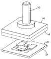
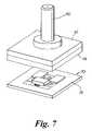
- FIG. 7shows the cover plate and base plate prior to assembly
- FIG. 8shows the module package assembly with a front optical connector and a rear electrical connector
- FIG. 9shows an alternative electrical connection arrangement.
- the base plate 20is a substantially flat tile approximately a few square mm in size and is typically made of a ceramic material with a planarity controlled to within +/ ⁇ 5 um.
- the use of a ceramic materialaids in the distribution of heat generated by any active components placed on the tile.
- Electrical tracks 22are disposed on the surface 25 of the tile according to the specific needs of the module.
- various components 24are attached to the tile at predetermined locations.
- An active optical component 26is also disposed on surface 25 of the tile at a predetermined location.
- materials other than ceramiccan be used, such as plastics or dielectric material, provided sufficient planarity is maintained.
- the components 24 and 26can be mounted using epoxy or alternatively, ultrasonic bonding. Components 24 and 26 can be than be electrically connected to tracks 22 using wire-bonding methods.
- flip chip bonding methodscan be employed in which ultrasonic power is used to attach the component or chip to the tile, thus reducing the possibility of contamination to the internal components that often occurs when epoxy or soldering methods are used. With this method it is possible to mechanically attach the components and at the same time create the electrical connections without the use adhesives or solder and thus simplify the process.
- the optical moduleis a receiver module and the active optical component 26 is a detector having an active area of 35 um for 10 Gb/s or less for higher bit rate.
- the detectormay be a PIN type detector or avalanche photodiode (APD).
- the detectorcan be mounted using the “flip chip” method.
- the optical moduleis a transmitter module and the active optical component 26 is a light source.
- the light sourcemay be a laser.
- the lasermay be a vertical cavity surface emitting (VCSEL) type laser.
- the lasercan be mounted using the “flip chip” method.
- the top plate 40is shown having a centrally located aperture 42 .
- the top platecan also be made from ceramic material or metal.
- a ferrule 50is disposed in the aperture 42 .
- Ferrulesare well known in the art as a means of holding optical fibres, which are typically disposed along a centrally located axis 52 of the ferrule.
- an antireflection coated flat ferrule or an angled ferrulecan be used.
- the ferrule 50is positioned within the aperture 42 so that it extends through the bottom surface 60 of the top plate 40 by a pre-determined distance.
- the accuracy of the axial alignment (Z direction) of the ferruleis within 5 microns. This is partly due to being able to position the ferrule without stress and at room temperature.
- the ferruleis inserted into the hole without any friction and positioned at the desired height thanks to a mechanical stop on a separate jig assembly.
- the correct Z alignmentrelies on the accurate positioning of the mechanical stop with respect to the bottom surface of the top plate.
- An adhesiveis then dispensed at the interface of the cover-ferrule and cured to fix the ferrule position in the Z direction.
- the room temperature processis able to guarantee a target alignment +/ ⁇ 5 um.
- a fibre(not shown) is located along the central axis 52 of the ferrule.
- the end of the fibreis polished so that it is substantially parallel with the end face 62 of the ferrule.
- the end of the optical fibremay also be polished so that it is substantially parallel to end face 64 of the ferrule or, alternatively, an angled ferrule can be used.
- the top plate 40is positioned over bottom plate 20 and aligned along the transversal plane (X and Y direction).
- a visual systemwhich allows images of the fibre cladding and the photodiode active area to overlap, is used to relatively align the two components with a precision of few microns (2–3 um).
- the top and bottom platesare than sealed together along the outer edges 48 and 28 of the plates.
- the precise alignment tolerances in X-Y directionis ensured by the planarity of the tile and cover base flat surfaces, thus ensuring intimate contact between the two parts without any drift, tilt or shift.
- the Z alignmentwas previously fixed.
- the sealis such that components 24 and detector 26 are protected from possible contamination by external sources. This typically means the package is hermetically sealed.
- the sealcan be achieved using epoxy or soldering techniques.
- the predetermined distance the ferrule protrudes through the aperture 42 and the accuracy to which the height of the detector 26 above the surface 25 of the base plate is knownensures that efficient butt coupling occurs between the fibre and detector. For example, a distance between the fibre and the detector of 50 um+/ ⁇ 10 um must be achieved.
- This passive alignment methodrequires no additional coupling optics, such as lenses and mirrors and uses fewer steps during the assembly process and is thus less expensive than other known active coupling techniques.
- the detector heightcan be controlled by using the flip chip mounting technique and by accurately knowing the thickness of the detector die.
- the ferrules distance from the covering platecan be controlled during assembly by referring to marks located on the cover plate and/or by using accurate micro-positioning equipment.
- the sealed module packagecan now have further optical connectors 82 disposed over the ferrule to establish optical connection to the rest of the communication system.
- electrical connectioncan be achieved using an electrical connector 85 attached to the under surface 84 of the base plate 20 .
- This electrical connectorcan be a flex connector.
- electrical leads 100can be used to establish electrical connection between the receiver package 120 and a print circuit board 125 .
- the spacing and thickness of these leadscan be chosen to reduce RF leakage from the receiver package and leave extra space for other electrical service connections.
- the use of leads instead of pinsensures furthermore a more flexible mechanical connection to the PCB.
Landscapes
- Physics & Mathematics (AREA)
- General Physics & Mathematics (AREA)
- Optics & Photonics (AREA)
- Light Receiving Elements (AREA)
- Optical Couplings Of Light Guides (AREA)
Abstract
Description
Claims (15)
Applications Claiming Priority (2)
| Application Number | Priority Date | Filing Date | Title |
|---|---|---|---|
| GB0303526AGB2398391A (en) | 2003-02-15 | 2003-02-15 | Connecting optic fibre to active component using two plates |
| GB0303526.8 | 2003-02-15 |
Publications (2)
| Publication Number | Publication Date |
|---|---|
| US20040161208A1 US20040161208A1 (en) | 2004-08-19 |
| US7093986B2true US7093986B2 (en) | 2006-08-22 |
Family
ID=9953093
Family Applications (1)
| Application Number | Title | Priority Date | Filing Date |
|---|---|---|---|
| US10/772,949Expired - LifetimeUS7093986B2 (en) | 2003-02-15 | 2004-02-05 | Low cost optical module |
Country Status (2)
| Country | Link |
|---|---|
| US (1) | US7093986B2 (en) |
| GB (1) | GB2398391A (en) |
Cited By (5)
| Publication number | Priority date | Publication date | Assignee | Title |
|---|---|---|---|---|
| US20060222302A1 (en)* | 2005-03-31 | 2006-10-05 | Frank Levinson | Power and communication interface for sensors using a single tethered fiber |
| US20060250276A1 (en)* | 2005-03-31 | 2006-11-09 | Finisar Corporation | Systems and methods for collecting data with sensors |
| US8834041B2 (en) | 2011-09-29 | 2014-09-16 | Corning Cable Systems Llc | Ferrule-based optical component assemblies |
| US9170387B2 (en) | 2011-09-29 | 2015-10-27 | Corning Cable Systems Llc | Optical component assemblies |
| US10928599B2 (en)* | 2018-05-09 | 2021-02-23 | Radiall | Optical sub-assembly for a module communicating over optical fiber, with a device for optical coupling aligned in a passive manner |
Families Citing this family (3)
| Publication number | Priority date | Publication date | Assignee | Title |
|---|---|---|---|---|
| GB2428104B (en) | 2005-07-07 | 2009-06-03 | Agilent Technologies Inc | Optoelectronic device |
| WO2007033611A1 (en)* | 2005-09-26 | 2007-03-29 | Hongkong Applied Science And Technology Research Institute Co., Ltd. | Opto-electronic device for optical fibre applications |
| CN102436042A (en)* | 2011-10-28 | 2012-05-02 | 江苏奥雷光电有限公司 | Flexible-coupling high-speed photoelectric device |
Citations (13)
| Publication number | Priority date | Publication date | Assignee | Title |
|---|---|---|---|---|
| JPS561577A (en) | 1979-06-19 | 1981-01-09 | Toshiba Corp | Light-driving semiconductor device |
| JPS5727064A (en) | 1980-07-25 | 1982-02-13 | Toshiba Corp | Optical thyristor device |
| JPS60107859A (en) | 1983-11-16 | 1985-06-13 | Fuji Electric Corp Res & Dev Ltd | Photo-driven semiconductor device |
| US4548466A (en) | 1982-09-29 | 1985-10-22 | Evans Dain S | Optical fibre coupling assemblies |
| US4741589A (en) | 1983-10-21 | 1988-05-03 | Alcatel N.V. | Coupler for optical waveguides |
| JPH02162305A (en) | 1988-12-15 | 1990-06-21 | Fujitsu Ltd | Optical fiber adjustment and fixing method |
| US5065011A (en) | 1989-07-20 | 1991-11-12 | Fujitsu Limited | Photodetector module for coupling with optical fiber |
| US6310707B1 (en)* | 1996-10-25 | 2001-10-30 | Seiko Epson Corporation | Optical wireless data communication system, and transmitter and receiver used therefor |
| US6364541B1 (en)* | 1999-12-22 | 2002-04-02 | New Focus, Inc. | Method and apparatus for optical reception |
| FR2815139A1 (en) | 2000-10-10 | 2002-04-12 | Commissariat Energie Atomique | Fibre optic connector or photon detector/emitter for telecommunications optics alignment, using component with auxiliary holes in outer component placed against fibre optic connector with alignment pegs |
| US20030077050A1 (en)* | 2000-10-25 | 2003-04-24 | Francois Marion | Method for passive alignment of supports, particularly plates bearing optical components |
| US6659659B1 (en)* | 2001-04-11 | 2003-12-09 | Optical Communication Products, Inc. | High-speed optical sub-assembly utilizing ceramic substrate, direct coupling and laser welding |
| US6786652B2 (en)* | 2001-12-19 | 2004-09-07 | Northrop Grumman Corporation | Process for fabricating a photonics package and for aligning an optical fiber with a photodetector surface during fabrication of such a package |
- 2003
- 2003-02-15GBGB0303526Apatent/GB2398391A/ennot_activeWithdrawn
- 2004
- 2004-02-05USUS10/772,949patent/US7093986B2/ennot_activeExpired - Lifetime
Patent Citations (13)
| Publication number | Priority date | Publication date | Assignee | Title |
|---|---|---|---|---|
| JPS561577A (en) | 1979-06-19 | 1981-01-09 | Toshiba Corp | Light-driving semiconductor device |
| JPS5727064A (en) | 1980-07-25 | 1982-02-13 | Toshiba Corp | Optical thyristor device |
| US4548466A (en) | 1982-09-29 | 1985-10-22 | Evans Dain S | Optical fibre coupling assemblies |
| US4741589A (en) | 1983-10-21 | 1988-05-03 | Alcatel N.V. | Coupler for optical waveguides |
| JPS60107859A (en) | 1983-11-16 | 1985-06-13 | Fuji Electric Corp Res & Dev Ltd | Photo-driven semiconductor device |
| JPH02162305A (en) | 1988-12-15 | 1990-06-21 | Fujitsu Ltd | Optical fiber adjustment and fixing method |
| US5065011A (en) | 1989-07-20 | 1991-11-12 | Fujitsu Limited | Photodetector module for coupling with optical fiber |
| US6310707B1 (en)* | 1996-10-25 | 2001-10-30 | Seiko Epson Corporation | Optical wireless data communication system, and transmitter and receiver used therefor |
| US6364541B1 (en)* | 1999-12-22 | 2002-04-02 | New Focus, Inc. | Method and apparatus for optical reception |
| FR2815139A1 (en) | 2000-10-10 | 2002-04-12 | Commissariat Energie Atomique | Fibre optic connector or photon detector/emitter for telecommunications optics alignment, using component with auxiliary holes in outer component placed against fibre optic connector with alignment pegs |
| US20030077050A1 (en)* | 2000-10-25 | 2003-04-24 | Francois Marion | Method for passive alignment of supports, particularly plates bearing optical components |
| US6659659B1 (en)* | 2001-04-11 | 2003-12-09 | Optical Communication Products, Inc. | High-speed optical sub-assembly utilizing ceramic substrate, direct coupling and laser welding |
| US6786652B2 (en)* | 2001-12-19 | 2004-09-07 | Northrop Grumman Corporation | Process for fabricating a photonics package and for aligning an optical fiber with a photodetector surface during fabrication of such a package |
Cited By (7)
| Publication number | Priority date | Publication date | Assignee | Title |
|---|---|---|---|---|
| US20060222302A1 (en)* | 2005-03-31 | 2006-10-05 | Frank Levinson | Power and communication interface for sensors using a single tethered fiber |
| US20060250276A1 (en)* | 2005-03-31 | 2006-11-09 | Finisar Corporation | Systems and methods for collecting data with sensors |
| US7859071B2 (en)* | 2005-03-31 | 2010-12-28 | Finisar Corporation | Power and communication interface for sensors using a single tethered fiber |
| US8154414B2 (en) | 2005-03-31 | 2012-04-10 | Finisar Corporation | Systems and methods for collecting data with sensors |
| US8834041B2 (en) | 2011-09-29 | 2014-09-16 | Corning Cable Systems Llc | Ferrule-based optical component assemblies |
| US9170387B2 (en) | 2011-09-29 | 2015-10-27 | Corning Cable Systems Llc | Optical component assemblies |
| US10928599B2 (en)* | 2018-05-09 | 2021-02-23 | Radiall | Optical sub-assembly for a module communicating over optical fiber, with a device for optical coupling aligned in a passive manner |
Also Published As
| Publication number | Publication date |
|---|---|
| GB0303526D0 (en) | 2003-03-19 |
| GB2398391A (en) | 2004-08-18 |
| US20040161208A1 (en) | 2004-08-19 |
Similar Documents
| Publication | Publication Date | Title |
|---|---|---|
| US5812717A (en) | Optical package with alignment means and method of assembling an optical package | |
| US6863444B2 (en) | Housing and mounting structure | |
| JP3329797B2 (en) | Method of manufacturing optoelectronic package and integrated mount | |
| US6867377B2 (en) | Apparatus and method of using flexible printed circuit board in optical transceiver device | |
| US9151916B2 (en) | Compact optical package made with planar structures | |
| US7021836B2 (en) | Attenuator and conditioner | |
| US20010017376A1 (en) | Optoelectronic assembly | |
| US6799902B2 (en) | Optoelectronic mounting structure | |
| US20020122637A1 (en) | Optical transmitter, receiver or transceiver module | |
| US7419311B2 (en) | Surface mount optical coupler, method of mounting the same, and method of producing the same | |
| US6905260B2 (en) | Method and apparatus for coupling optical elements to optoelectronic devices for manufacturing optical transceiver modules | |
| US6896422B2 (en) | Optoelectronic modules and methods of manufacturing the same | |
| US7093986B2 (en) | Low cost optical module | |
| US7437038B2 (en) | Z-axis alignment of an optoelectronic component using a spacer tool | |
| KR100347521B1 (en) | Silicon optical bench and plastic molded receptacle for reception it and optical subassembly constructed them | |
| US6948860B1 (en) | Optical subassembly for optoelectronic devices | |
| WO2002103426A2 (en) | Optical power control system | |
| US20010033720A1 (en) | System and method for aligning optical components | |
| WO2003001254A2 (en) | Apparatus for holding an optical element | |
| JP2021043469A (en) | Optical coupling method | |
| US20020131716A1 (en) | Optical subassembly and method of alignment thereof |
Legal Events
| Date | Code | Title | Description |
|---|---|---|---|
| AS | Assignment | Owner name:AGILENT TECHNOLOGIES, INC., CALIFORNIA Free format text:ASSIGNMENT OF ASSIGNORS INTEREST;ASSIGNOR:AGILENT TECHNOLOGIES ITALIA S.P.A.;REEL/FRAME:014965/0114 Effective date:20040130 | |
| AS | Assignment | Owner name:AVAGO TECHNOLOGIES GENERAL IP PTE. LTD.,SINGAPORE Free format text:ASSIGNMENT OF ASSIGNORS INTEREST;ASSIGNOR:AGILENT TECHNOLOGIES, INC.;REEL/FRAME:017206/0666 Effective date:20051201 Owner name:AVAGO TECHNOLOGIES GENERAL IP PTE. LTD., SINGAPORE Free format text:ASSIGNMENT OF ASSIGNORS INTEREST;ASSIGNOR:AGILENT TECHNOLOGIES, INC.;REEL/FRAME:017206/0666 Effective date:20051201 | |
| AS | Assignment | Owner name:AVAGO TECHNOLOGIES FIBER IP (SINGAPORE) PTE. LTD., Free format text:ASSIGNMENT OF ASSIGNORS INTEREST;ASSIGNOR:AVAGO TECHNOLOGIES GENERAL IP (SINGAPORE) PTE. LTD.;REEL/FRAME:017675/0294 Effective date:20051201 | |
| STCF | Information on status: patent grant | Free format text:PATENTED CASE | |
| FPAY | Fee payment | Year of fee payment:4 | |
| FPAY | Fee payment | Year of fee payment:8 | |
| AS | Assignment | Owner name:DEUTSCHE BANK AG NEW YORK BRANCH, AS COLLATERAL AGENT, NEW YORK Free format text:PATENT SECURITY AGREEMENT;ASSIGNOR:AVAGO TECHNOLOGIES GENERAL IP (SINGAPORE) PTE. LTD.;REEL/FRAME:032851/0001 Effective date:20140506 Owner name:DEUTSCHE BANK AG NEW YORK BRANCH, AS COLLATERAL AG Free format text:PATENT SECURITY AGREEMENT;ASSIGNOR:AVAGO TECHNOLOGIES GENERAL IP (SINGAPORE) PTE. LTD.;REEL/FRAME:032851/0001 Effective date:20140506 | |
| AS | Assignment | Owner name:AVAGO TECHNOLOGIES GENERAL IP (SINGAPORE) PTE. LTD., SINGAPORE Free format text:TERMINATION AND RELEASE OF SECURITY INTEREST IN PATENT RIGHTS (RELEASES RF 032851-0001);ASSIGNOR:DEUTSCHE BANK AG NEW YORK BRANCH, AS COLLATERAL AGENT;REEL/FRAME:037689/0001 Effective date:20160201 Owner name:AVAGO TECHNOLOGIES GENERAL IP (SINGAPORE) PTE. LTD Free format text:TERMINATION AND RELEASE OF SECURITY INTEREST IN PATENT RIGHTS (RELEASES RF 032851-0001);ASSIGNOR:DEUTSCHE BANK AG NEW YORK BRANCH, AS COLLATERAL AGENT;REEL/FRAME:037689/0001 Effective date:20160201 | |
| AS | Assignment | Owner name:BANK OF AMERICA, N.A., AS COLLATERAL AGENT, NORTH CAROLINA Free format text:PATENT SECURITY AGREEMENT;ASSIGNOR:AVAGO TECHNOLOGIES GENERAL IP (SINGAPORE) PTE. LTD.;REEL/FRAME:037808/0001 Effective date:20160201 Owner name:BANK OF AMERICA, N.A., AS COLLATERAL AGENT, NORTH Free format text:PATENT SECURITY AGREEMENT;ASSIGNOR:AVAGO TECHNOLOGIES GENERAL IP (SINGAPORE) PTE. LTD.;REEL/FRAME:037808/0001 Effective date:20160201 | |
| AS | Assignment | Owner name:AVAGO TECHNOLOGIES GENERAL IP (SINGAPORE) PTE. LTD Free format text:CORRECTIVE ASSIGNMENT TO CORRECT THE ASSIGNEE NAME PREVIOUSLY RECORDED AT REEL: 017206 FRAME: 0666. ASSIGNOR(S) HEREBY CONFIRMS THE ASSIGNMENT;ASSIGNOR:AGILENT TECHNOLOGIES, INC.;REEL/FRAME:038632/0662 Effective date:20051201 | |
| AS | Assignment | Owner name:AVAGO TECHNOLOGIES GENERAL IP (SINGAPORE) PTE. LTD., SINGAPORE Free format text:TERMINATION AND RELEASE OF SECURITY INTEREST IN PATENTS;ASSIGNOR:BANK OF AMERICA, N.A., AS COLLATERAL AGENT;REEL/FRAME:041710/0001 Effective date:20170119 Owner name:AVAGO TECHNOLOGIES GENERAL IP (SINGAPORE) PTE. LTD Free format text:TERMINATION AND RELEASE OF SECURITY INTEREST IN PATENTS;ASSIGNOR:BANK OF AMERICA, N.A., AS COLLATERAL AGENT;REEL/FRAME:041710/0001 Effective date:20170119 | |
| MAFP | Maintenance fee payment | Free format text:PAYMENT OF MAINTENANCE FEE, 12TH YEAR, LARGE ENTITY (ORIGINAL EVENT CODE: M1553) Year of fee payment:12 | |
| AS | Assignment | Owner name:AVAGO TECHNOLOGIES INTERNATIONAL SALES PTE. LIMITE Free format text:MERGER;ASSIGNOR:AVAGO TECHNOLOGIES GENERAL IP (SINGAPORE) PTE. LTD.;REEL/FRAME:047196/0097 Effective date:20180509 | |
| AS | Assignment | Owner name:AVAGO TECHNOLOGIES INTERNATIONAL SALES PTE. LIMITE Free format text:CORRECTIVE ASSIGNMENT TO CORRECT THE EXECUTION DATE PREVIOUSLY RECORDED AT REEL: 047196 FRAME: 0097. ASSIGNOR(S) HEREBY CONFIRMS THE MERGER;ASSIGNOR:AVAGO TECHNOLOGIES GENERAL IP (SINGAPORE) PTE. LTD.;REEL/FRAME:048555/0510 Effective date:20180905 | |
| AS | Assignment | Owner name:BROADCOM INTERNATIONAL PTE. LTD., SINGAPORE Free format text:ASSIGNMENT OF ASSIGNORS INTEREST;ASSIGNOR:AVAGO TECHNOLOGIES INTERNATIONAL SALES PTE. LIMITED;REEL/FRAME:053771/0901 Effective date:20200826 | |
| AS | Assignment | Owner name:AVAGO TECHNOLOGIES INTERNATIONAL SALES PTE. LIMITED, SINGAPORE Free format text:MERGER;ASSIGNORS:AVAGO TECHNOLOGIES INTERNATIONAL SALES PTE. LIMITED;BROADCOM INTERNATIONAL PTE. LTD.;REEL/FRAME:062952/0850 Effective date:20230202 |