US7091551B1 - Four-bit FinFET NVRAM memory device - Google Patents
Four-bit FinFET NVRAM memory deviceDownload PDFInfo
- Publication number
- US7091551B1 US7091551B1US10/907,712US90771205AUS7091551B1US 7091551 B1US7091551 B1US 7091551B1US 90771205 AUS90771205 AUS 90771205AUS 7091551 B1US7091551 B1US 7091551B1
- Authority
- US
- United States
- Prior art keywords
- gate
- bit memory
- source
- drain
- bit
- Prior art date
- Legal status (The legal status is an assumption and is not a legal conclusion. Google has not performed a legal analysis and makes no representation as to the accuracy of the status listed.)
- Expired - Lifetime
Links
Images


Classifications
- G—PHYSICS
- G11—INFORMATION STORAGE
- G11C—STATIC STORES
- G11C16/00—Erasable programmable read-only memories
- G11C16/02—Erasable programmable read-only memories electrically programmable
- G11C16/04—Erasable programmable read-only memories electrically programmable using variable threshold transistors, e.g. FAMOS
- G11C16/0466—Erasable programmable read-only memories electrically programmable using variable threshold transistors, e.g. FAMOS comprising cells with charge storage in an insulating layer, e.g. metal-nitride-oxide-silicon [MNOS], silicon-oxide-nitride-oxide-silicon [SONOS]
- G11C16/0475—Erasable programmable read-only memories electrically programmable using variable threshold transistors, e.g. FAMOS comprising cells with charge storage in an insulating layer, e.g. metal-nitride-oxide-silicon [MNOS], silicon-oxide-nitride-oxide-silicon [SONOS] comprising two or more independent storage sites which store independent data
- H—ELECTRICITY
- H10—SEMICONDUCTOR DEVICES; ELECTRIC SOLID-STATE DEVICES NOT OTHERWISE PROVIDED FOR
- H10B—ELECTRONIC MEMORY DEVICES
- H10B41/00—Electrically erasable-and-programmable ROM [EEPROM] devices comprising floating gates
- H10B41/30—Electrically erasable-and-programmable ROM [EEPROM] devices comprising floating gates characterised by the memory core region
- H—ELECTRICITY
- H10—SEMICONDUCTOR DEVICES; ELECTRIC SOLID-STATE DEVICES NOT OTHERWISE PROVIDED FOR
- H10B—ELECTRONIC MEMORY DEVICES
- H10B69/00—Erasable-and-programmable ROM [EPROM] devices not provided for in groups H10B41/00 - H10B63/00, e.g. ultraviolet erasable-and-programmable ROM [UVEPROM] devices
- H—ELECTRICITY
- H10—SEMICONDUCTOR DEVICES; ELECTRIC SOLID-STATE DEVICES NOT OTHERWISE PROVIDED FOR
- H10D—INORGANIC ELECTRIC SEMICONDUCTOR DEVICES
- H10D30/00—Field-effect transistors [FET]
- H10D30/60—Insulated-gate field-effect transistors [IGFET]
- H10D30/68—Floating-gate IGFETs
- H10D30/687—Floating-gate IGFETs having more than two programming levels
- H—ELECTRICITY
- H10—SEMICONDUCTOR DEVICES; ELECTRIC SOLID-STATE DEVICES NOT OTHERWISE PROVIDED FOR
- H10D—INORGANIC ELECTRIC SEMICONDUCTOR DEVICES
- H10D30/00—Field-effect transistors [FET]
- H10D30/01—Manufacture or treatment
- H10D30/021—Manufacture or treatment of FETs having insulated gates [IGFET]
- H10D30/024—Manufacture or treatment of FETs having insulated gates [IGFET] of fin field-effect transistors [FinFET]
- H—ELECTRICITY
- H10—SEMICONDUCTOR DEVICES; ELECTRIC SOLID-STATE DEVICES NOT OTHERWISE PROVIDED FOR
- H10D—INORGANIC ELECTRIC SEMICONDUCTOR DEVICES
- H10D30/00—Field-effect transistors [FET]
- H10D30/60—Insulated-gate field-effect transistors [IGFET]
- H10D30/62—Fin field-effect transistors [FinFET]
- Y—GENERAL TAGGING OF NEW TECHNOLOGICAL DEVELOPMENTS; GENERAL TAGGING OF CROSS-SECTIONAL TECHNOLOGIES SPANNING OVER SEVERAL SECTIONS OF THE IPC; TECHNICAL SUBJECTS COVERED BY FORMER USPC CROSS-REFERENCE ART COLLECTIONS [XRACs] AND DIGESTS
- Y10—TECHNICAL SUBJECTS COVERED BY FORMER USPC
- Y10S—TECHNICAL SUBJECTS COVERED BY FORMER USPC CROSS-REFERENCE ART COLLECTIONS [XRACs] AND DIGESTS
- Y10S438/00—Semiconductor device manufacturing: process
- Y10S438/954—Making oxide-nitride-oxide device
Definitions
- the present inventionrelates to the field of FinFET memory devices; more specifically, it relates to a FinFET device capable of storing four independent bit values, a method of fabricating the FinFET device and a flash memory array using the FinFET device.
- the present inventionforms two charge storage regions in a dielectric layer on a first sidewall of a fin of a FinFET and two additional charge storage regions in a dielectric layer on a second sidewall of the fin, the first and second sidewalls being opposite of another.
- a first aspect of the present inventionis a semiconductor device, comprising: a fin body having opposite first and second ends and opposite first and second sidewalls, the first and second sidewalls disposed between the first and second ends; a first gate dielectric stack disposed on the first sidewall and a second gate dielectric stack disposed on the second sidewall, the first and second stacks each comprising at least a first, a second and a third dielectric layer, the first dielectric layer of the first dielectric stack in direct physical contact with the first sidewall and the first dielectric layer of the second dielectric stack in direct physical contact with the second sidewall; a first gate electrode in direct physical contact with the third dielectric layer of the first gate dielectric stack and a second gate electrode in direct physical contact with the third dielectric layer of the second gate dielectric stack, the first and second gate electrodes not in direct physical contact with each other; a first source/drain in the first end of the fin body and a second source/drain in the second end of the fin body; and a channel region in the fin body between the
- a second aspect of the present inventionis a method of fabricating a semiconductor device, comprising: providing a silicon layer on top surface of an insulation layer of a substrate; forming a fin body from the silicon layer, the fin body having opposite first and second ends and opposite first and second sidewalls, the first and second sidewalls disposed between the first and second ends; forming a first gate dielectric stack on the first sidewall and a second gate dielectric stack on the second sidewall, the first and second stacks each comprising at least a first, a second and a third dielectric layer, the first dielectric layer of the first dielectric stack in direct physical contact with the first sidewall and the first dielectric layer of the second dielectric stack in direct physical contact with the second sidewall; forming a first gate electrode in direct physical contact with the third dielectric layer of the first gate dielectric stack and a second gate electrode in direct physical contact with the third dielectric layer of the second gate dielectric stack, the first and second gate electrodes not in direct physical contact with each other; and forming a first source/drain
- a third aspect of the present inventionis an NVRAM memory, comprising: an array of four-bit memory cells arranged in rows and columns, each 4-bit memory cell comprising: a fin body having opposite first and second ends and opposite first and second sidewalls, the first and second sidewalls disposed between the first and second ends; a first gate dielectric stack disposed on the first sidewall and a second gate dielectric stack disposed on the second sidewall, the first and second stacks each comprising at least a first, a second and a third dielectric layer, the first dielectric layer of the first dielectric stack in direct physical contact with the first sidewall and the first dielectric layer of the second dielectric stack in direct physical contact with the second sidewall; a first gate electrode in direct physical contact with the third dielectric layer of the first gate dielectric stack and a second gate electrode in direct physical contact with the third dielectric layer of the second gate dielectric stack, the first and second gate electrodes not in direct physical contact with each other; a first source/drain in the first end of the fin body and a second
- FIG. 1is flowchart of an exemplary method of fabricating a four-bit FinFET device according to the present invention
- FIGS. 2A through 2Fare partial cross-sectional drawings illustrating an exemplary method for fabricating a silicon fin portion of the four-bit FinFET device of the present invention
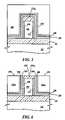
- FIGS. 3 through 6are partial cross-sectional drawings illustrating additional steps for fabricating the four-bit FinFET device of the present invention
- FIG. 7is a top view and FIGS. 8 and 9 are cross-sectional views through lines 8 — 8 and 9 — 9 respectively of FIG. 7 illustrating the additional step of forming doped regions in the fin portion of the four-bit FinFET device of the present invention
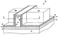
- FIG. 10is an isometric view illustrating the additional step of forming the gate electrodes of the four-bit FinFET device of the present invention.
- FIG. 11is a plan view through section line 11 of FIG. 10 , illustrating the bit storage locations of the four-bit FinFET device of the present invention
- FIG. 12Ais schematic diagram of a Non-Volatile Random Access Memory (NVRAM) according to the present invention.
- FIG. 12Bis a physical layout of a portion of the NVRAM of FIG. 12B .
- FIG. 1is flowchart of an exemplary method of fabricating a four-bit FinFET device according to the present invention.
- a silicon-on-insulator (SOI) substrateis provided and in step 105 , a silicon fin is formed from the silicon layer of the SOI substrate.
- Steps 100 and 105are illustrated in FIGS. 2A through 2F and described in more detail infra.
- a multi-layer gate dielectric stackis formed on opposite sides of the silicon fin.
- the multi-layer gate dielectric stackcomprises three distinct dielectric layers.
- the dielectric layer in contact with the silicon finmay also be referred to as a tunneling gate dielectric layer.
- the inner dielectric layer of the multi-layer gate dielectric stackmay be referred to a charge storing dielectric layer (i.e. a dielectric layer capable of storing either a negative or positive charge formed by application of a voltage across the chargeable dielectric layer and from which the charge can be removed by application of a reverse polarity voltage across the charge storing dielectric layer).
- Step 110is illustrated in FIGS. 3 and 4 and described in more detail infra.
- a gate layeris formed over the silicon fin and in step 120 , particularly on the sidewalls of the fin, and the gate layer is removed from over the silicon fin. Steps 115 and 120 are illustrated in FIGS. 5 and 6 and described in more detail infra.
- source/drain regionsare formed in opposite ends of the silicon fin, separated by a channel region. Formation of source/drain regions are illustrated in FIGS. 7 through 9 and described in more detail infra.
- step 130the gate layer is etched to form two electrically un-connected gate electrodes on opposite sidewalls of the silicon fin and aligned between the source/drain regions previously formed in the silicon fin.
- the now essentially completed four-bit FinFET deviceis illustrated in FIG. 10 and described in more detail infra.
- step 135contacts are formed to the source/drains and gates and wires connected to the contacts to interconnect the four-bit FinFET as a cell of a memory array.
- An exemplary memory array using four-bit FinFETsis illustrated in FIG. 12 .
- FIGS. 2A through 2Fare partial cross-sectional drawings illustrating an exemplary method for fabricating a silicon fin portion of the four-bit FinFET device of the present invention.
- an SOI substratecomprises a buried dielectric layer 145 separating a overlaying single-crystal silicon layer 150 from an underlying substrate 155 .
- buried dielectric layer 145comprises a buried oxide (BOX) such silicon dioxide.
- substrate 155comprises single crystal silicon.
- Silicon layer 150may be intrinsic, doped N-type or doped P type.
- FIGS. 2B through 2Fillustrate a technique of forming fins of a FinFET by a process known as sidewall transfer.
- a hard mask layer 160is formed on a top surface 165 of silicon layer 150 .
- hard mask layer 160comprises silicon dioxide formed, for example by a chemical vapor deposition (CVD) process.
- Hard mask layerhas a thickness T and acts as a chemical-mechanical-polish (CMP) stop in the process described infra in reference to FIG. 6 .
- CMPchemical-mechanical-polish
- a photolithographic processis used to pattern a photoresist layer (not shown) which is used as a mask for etching hard mask layer 160 of FIG. 2B into an island 170 , followed by removal of the photoresist layer.
- the etch processis a reactive ion etch (RIE) selective to silicon dioxide over silicon (that is, preferentially etching silicon dioxide at a faster rate than silicon)
- spacers 175are formed on sidewalls 180 of island 170 .
- Spacers 175may be formed by deposition of a conformal layer, for example by CVD, followed by a direction RIE to remove the conformal layer from a top surface 185 of island 170 and top surface 190 of silicon layer 150 .
- the width W of spacers 175can be controlled by adjustment of the thickness T of hard mask layer 160 (see FIG. 2B ) from which island 170 was formed, the thickness of the conformal layer deposited from which spacers 175 where formed, and the RIE etch time and process conditions.
- spacers 175comprise silicon nitride.
- island 170(see FIG. 2D ) is removed, for example by an RIE process selective to silicon dioxide over silicon and silicon nitride.
- a thin layer of thermal oxidemay be grown on exposed top surface 190 of silicon layer 150 prior to the etch operation to enhance the selectivity.
- fins 195are formed on top surface 200 of buried dielectric layer 145 by, for example when spacers 175 comprise silicon nitride, an RIE process selective to silicon over silicon nitride. Some etching of spacers 175 (see FIG. 2E ) to form dielectric caps 175 A on top surfaces 205 of fins 195 may occur.
- a structure similar to that depicted in FIG. 2Fmay be formed by forming a first layer on top surface of an the upper silicon layer of an SOI substrate, forming a second layer on top of the first layer, etching the second to form islands, undercutting the second layer under the islands, etching the silicon layer to form fins and removing the island, but not the remaining first layer on top of the fin.
- FIGS. 3 through 6are partial cross-sectional drawings illustrating additional steps for fabricating the four-bit FinFET device of the present invention.
- a first gate dielectric layer 210is formed on sidewalls 215 of fin 195 .
- first gate dielectric layer 210comprises thermal silicon dioxide and is between about 35 ⁇ to about 105 ⁇ thick.
- first gate dielectric layermay be formed by deposition, in which case the first dielectric layer will be formed on exposed surfaces of dielectric cap 175 A as well.
- a second gate dielectric layer 220is formed on a top surface 225 of first dielectric layer 210 and exposed surfaces (including top surface 205 ) of dielectric cap layer 175 A.
- second gate dielectric layer 220comprises CVD silicon nitride and is between about 75 ⁇ to about 225 ⁇ thick.
- a third gate dielectric layer 230is formed on a top surface 235 of second gate dielectric layer 220 .
- third gate dielectric layer 230comprises CVD silicon dioxide and is between about 25 ⁇ to about 75 ⁇ thick.
- First and third gate dielectric layers 220 and 230may independently comprise high K (where K is the dielectric constant) dielectric materials, where a high K dielectric material has a relative permittivity above 10.
- First and third gate dielectric layers 220 and 230may independently comprise high K dielectric materials in combination with silicon dioxide.
- high K dielectric materialsinclude but are not limited metal oxides such as Ta 2 O 5 , BaTiO 3 , HfO 2 , ZrO 2 , Al 2 O 3 , or metal silicates such as HfSi x O y or HfSi x O y N z or combinations thereof.
- Second gate dielectric layer 220is the “chargeable dielectric” mentioned supra in reference to step 115 of FIG. 1
- a CVD polysilicon layer 245is formed on a top surface 240 of third gate dielectric layer 230 .
- polysilicon layer 245is thicker than the thickness of fin 195 and dielectric cap 175 A combined.
- polysilicon layer 245is undoped.
- polysilicon layer 245is doped N-type if the completed FinFET is to be a N-channel FinFET (FinNFET).
- polysilicon layer 245is doped P-type if the completed FinFET is to be a P-Channel (FinPFET).
- a CMP processis performed to thin polysilicon layer 245 of FIG. 5 , such that top surface 205 of dielectric cap 175 A is coplanar with a top surface 250 of a polysilicon layer 245 A and coplanar with exposed ends 265 and 260 of second and third gate dielectric layers 220 and 230 respectively.
- FIG. 7is a top view and FIGS. 8 and 9 are cross-sectional views through lines 8 — 8 and 9 — 9 respectively of FIG. 7 illustrating the additional step of forming doped regions in the fin portion of the four-bit FinFET device of the present invention.
- a patterned photo resist layer 265is formed perpendicular to fin 195 on top of capping layer 175 A, and any exposed second and third gate dielectric layer 220 and 230 . Then an ion implantation is performed of species X. Photoresist layer 265 is of sufficient thickness to stop any species X from penetrating into polysilicon layer 245 A. However, as seen in FIG.
- species Xpenetrates into fin 195 forming first and second source/drain (S/D) regions 270 A and 270 B respectively, in fin 195 .
- species Xcomprises an N-dopant species if the completed FinFET is to be a FinNFET.
- species Xcomprise a P-dopant species if the completed FinFET is to be a FinPFET. Since photoresist layer 265 will also be used as mask to etch silicon layer 245 A to form gate electrodes, a channel region 275 is defined between S/D regions 270 A and 270 B.
- FIG. 10is an isometric view after the additional step of forming the gate electrodes of the four-bit FinFET device of the present invention.
- a polysilicon etchfor example a RIE selective silicon to silicon dioxide and silicon nitride
- photoresist layer 265see FIGS. 7 , 8 and 9
- silicon layer 245 Asee FIGS. 7 , 8 and 9
- FIG. 11is a plan view through section line 11 of FIG. 10 , illustrating the bit storage locations of the four-bit FinFET device of the present invention.
- four-bit FinFET 285includes opposing first gate electrode 280 A (GATE 1 ), second gate electrode 280 B (GATE 2 ), first S/D regions 270 A (S/D 1 ) second S/D region 270 B (S/D 2 ) and channel region 275 .
- a first charge storage region 290 A (BIT 1 )is located in second dielectric layer 220 between first gate electrode 280 A (GATE 1 ) and channel 275 and adjacent to first S/D region 270 A (S/D 1 ).
- a second charge storage region 290 B(BIT 2 ) is located in second dielectric layer 220 between first gate 280 A (GATE 1 ) and channel 275 and adjacent to second S/D 270 B (S/D 2 ).
- a third charge storage region 290 C(BIT 3 ) is located in second dielectric layer 220 between second gate electrode 280 B (GATE 2 ) and channel 275 and adjacent to first S/D region (S/D 1 ).
- a fourth charge storage region 290 D (BIT 4 )is located in second dielectric layer 220 between second gate electrode 280 B (GATE 2 ) and channel 275 and adjacent to second S/D region 270 B (S/D 2 ).
- Four-bits of datamay be independently written to or read from BIT 1 , BIT 2 , BIT 3 and BIT 4 by application of the voltages at the levels indicated to GATE 1 , GATE 2 , S/D 1 and S/D 2 as illustrated in Table I.
- To write a bitmeans to place charge on the bit. The charge written may be positive or negative. However, BIT 1 , BIT 2 , BIT 3 and BIT 4 must be erased at the same time. To erase a bit means to remove the charge that was written and return the bit to an uncharged state.
- any unwritten BITPrior to erasing BIT 1 , BIT 2 , BIT 3 and BIT 4 , any unwritten BIT may be written to so that no uncharged bits are subject to over-erasing which could result in low charge levels of the bit upon the next write cycle.
- the voltages listed in Table Iare suitable for a FinNFET storing negative charge (electrons) in the bit locations and having a first or tunneling gate dielectric layer comprising silicon dioxide about 70 ⁇ thick, a second gate dielectric layer comprising silicon nitride about 150 ⁇ thick and a third gate dielectric comprising silicon dioxide about 50 ⁇ thick.
- FinFET 285is suitable for use as a memory cell in a non-volatile random access memory (NVRAM).
- NVRAMnon-volatile random access memory
- Examples of NVRAMinclude FLASH, electrically erasable reprogrammable read only memory (EEPROM) and electrically programmable read-only memory (EPROM).
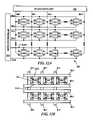
- FIG. 12Ais schematic diagram of a NVRAM according to the present invention.
- a NVRAM 300includes an N by M array of four 4-bit NVRAM memory cells C 00 –CMN of M rows and N columns. Each four-bit NVRAM memory cell C 00 –CMN includes a FINFET 285 as illustrated in FIGS. 10 and 11 supra.
- NVRAM 300includes a bitline controller 305 and a wordline controller 305 that decode I/Os during various operations that are performed on NVRAM 300 (e.g., operations such as programming, reading, verifying, erasing).
- Bitline controller 305 and wordline controller 310receive address bus information from a system controller (not shown) or the like.
- a common wordlineis attached to the gate of each cell in a row, such as wordlines WL 0 , WL 1 , WL 2 , through WLM.
- a common bitlineis attached to each bit of a cell in a column, such as bitlines BL 0 , BL 1 , BL 2 through BLN.
- FIG. 12Ait can be seen that a first set of two of the four bits of each cell are connected to a first wordline and a second set of two of the four bits (different from the two bits of the first set) are connected to a second wordline.
- bit B 0 and B 1are connected to wordline WL 0 and bits B 2 and B 3 are connected to WL 1 .
- one bit of each cellare connected to a first bitline and the other bit of each cell is connected to a second bitline.
- bit B 0 and B 21are connected to wordline BWL 0 and bits B 1 and B 3 are connected to BL 1 . Physically, it is important to distinguish between bits as illustrated in FIG. 12B and described infra.
- Table IIillustrates one particular set of voltage parameters for performing reading, programming and single sided erases of the four-bit memory cell C 00 having a first bit C 0 , a second bit B 1 , a third bit B 2 and a fourth bit B 3 .
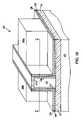
- FIG. 12Bis a physical layout of a portion of the NVRAM of FIG. 12B .
- four-bit memory cells C 00 , C 01 , C 02 , C 10 , C 11 and C 12bitlines BL 0 , BL 1 and BL 3 , and wordlines WL 0 , WL 2 , WL 3 and WL 4 are illustrated.
- 4-bit memory cell C 00as an example, it can be seen that bits B 0 and B 1 are stored in a dielectric layer 315 A on a first side of a fin body 320 and bits B 1 and B 3 are stored in a dielectric layer 315 B on a second and opposite side of the fin body.
- WL 0forms a common gate for bits B 0 and B 1 and WL 1 forms a common gate for bits B 2 and B 3 .
- Bitline BL 0forms a common source for bits B 0 and B 2 and bitline BL 1 forms a common drain for bits B 1 and B 3 .
- bitline BL 1also forms a common source for Bits B 0 and B 2 of adjacent four-bit memory cell C 01 . It is a feature of the present invention that the drain of two bits in a first four-bit cell is also the source of two bits in the adjacent four-bit cell second between each pair of wordlines acting a pair of common gates for those four-bit cells.
- the present inventionprovides a device with both increased device density and increased bit counts per memory cell device at the same time.
Landscapes
- Engineering & Computer Science (AREA)
- Microelectronics & Electronic Packaging (AREA)
- Non-Volatile Memory (AREA)
- Semiconductor Memories (AREA)
Abstract
Description
| GATE | ||||
| 1 | GATE 2 | S/D 1 | S/ | |
| OPERATION | VOLTAGE | VOLTAGE | VOLTAGE | |
| WRITE BIT | ||||
| 1 | 6 V | 2.5 V | 5 V | 0 |
| READ BIT | ||||
| 1 | 2.5 V | 0 V | 0 V | 0.5 |
| WRITE BIT | ||||
| 2 | 6 V | 2.5 V | 0 V | 5 |
| READ BIT | ||||
| 2 | 2.5 V | 0 V | 0.5 V | 0 |
| WRITE BIT | ||||
| 3 | 2.5 V | 6 V | 5 V | 0 |
| READ BIT | ||||
| 3 | 0 V | 2.5 V | 0 V | 0.5 |
| WRITE BIT | ||||
| 4 | 2.5 V | 6 V | 0 V | 5 |
| READ BIT | ||||
| 4 | 0 V | 2.5 V | 0.5 V | 0 V |
| ERASE BITS | −6 V | −6 V | 5.5 V | 5.5 V |
| TABLE II | |||||
| GATE | GATE | ||||
| VOL- | VOL- | ||||
| OPERA- | TAGE | TAGE | BITLINE 0 | ||
| TION | WL0 | WL1 | VOLTAGE | VOLTAGE | COMMENT |
| READ | 2.5 V | 0 V | 0 V | 0.5 V | |
| BIT B0 | |||||
| READ | 2.5 V | 0 V | 0.5 V | 0 V | |
| BIT B1 | |||||
| READ | 0 V | 2.5 V | 0 V | 0.5 V | |
| BIT B2 | |||||
| READ | 0 V | 2.5 V | 0.5 V | 0 V | |
| BIT B3 | |||||
| WRITE | 6 V | 2.5 V | 5 V | 0 V | Hot Electron |
| BIT B0 | |||||
| WRITE | 6 V | 2.5 V | 0 V | 5 V | Hot |
| BIT B1 | Electron | ||||
| WRITE | 2.5 V | 6 V | 5 V | 0 V | Hot |
| BIT B2 | Electron | ||||
| WRITE | 2.5 V | 6 V | 0 V | 5 V | Hot |
| BIT B3 | Electron | ||||
| ERASE | −6 V | 0 V | 5.5 V | Float | Hot Hole |
| BIT B0 | |||||
| ERASE | −6 V | 0 V | Float | 5.5 V | Hot Hole |
| BIT B1 | |||||
| ERASE | 0 V | −6 V | 5.5 V | Float | Hot Hole |
| BIT B2 | |||||
| ERASE | 0 V | −6 V | Float | 5.5 V | Hot Hole |
| BIT B3 | |||||
| ERASE | −6 V | 0 V | 5.5 V | 5.5 V | |
| BITS | |||||
| B0 & B1 | |||||
| ERASE | 0 V | −6 V | 5.5 V | 5.5 V | |
| BITS | |||||
| B2 & B3 | |||||
Claims (22)
Priority Applications (2)
| Application Number | Priority Date | Filing Date | Title |
|---|---|---|---|
| US10/907,712US7091551B1 (en) | 2005-04-13 | 2005-04-13 | Four-bit FinFET NVRAM memory device |
| US11/426,623US7416941B2 (en) | 2005-04-13 | 2006-06-27 | Four-bit finfet NVRAM memory device |
Applications Claiming Priority (1)
| Application Number | Priority Date | Filing Date | Title |
|---|---|---|---|
| US10/907,712US7091551B1 (en) | 2005-04-13 | 2005-04-13 | Four-bit FinFET NVRAM memory device |
Related Child Applications (1)
| Application Number | Title | Priority Date | Filing Date |
|---|---|---|---|
| US11/426,623DivisionUS7416941B2 (en) | 2005-04-13 | 2006-06-27 | Four-bit finfet NVRAM memory device |
Publications (1)
| Publication Number | Publication Date |
|---|---|
| US7091551B1true US7091551B1 (en) | 2006-08-15 |
Family
ID=36781732
Family Applications (2)
| Application Number | Title | Priority Date | Filing Date |
|---|---|---|---|
| US10/907,712Expired - LifetimeUS7091551B1 (en) | 2005-04-13 | 2005-04-13 | Four-bit FinFET NVRAM memory device |
| US11/426,623Expired - Fee RelatedUS7416941B2 (en) | 2005-04-13 | 2006-06-27 | Four-bit finfet NVRAM memory device |
Family Applications After (1)
| Application Number | Title | Priority Date | Filing Date |
|---|---|---|---|
| US11/426,623Expired - Fee RelatedUS7416941B2 (en) | 2005-04-13 | 2006-06-27 | Four-bit finfet NVRAM memory device |
Country Status (1)
| Country | Link |
|---|---|
| US (2) | US7091551B1 (en) |
Cited By (110)
| Publication number | Priority date | Publication date | Assignee | Title |
|---|---|---|---|---|
| US20050242391A1 (en)* | 2004-05-03 | 2005-11-03 | The Regents Of The University Of California | Two bit/four bit SONOS flash memory cell |
| US20060234456A1 (en)* | 2005-04-13 | 2006-10-19 | Anderson Brent A | Four-bit finfet nvram memory device |
| US20060292781A1 (en)* | 2005-06-23 | 2006-12-28 | Samsung Electronics Co., Ltd. | Finfets, nonvolatile memory devices including finfets, and methods of forming the same |
| US20070018237A1 (en)* | 2005-07-22 | 2007-01-25 | Samsung Electronics Co., Ltd. | Non-volatile memory device having fin-type channel region and method of fabricating the same |
| US20080080245A1 (en)* | 2005-05-19 | 2008-04-03 | Chih-Cheng Liu | P-channel memory and operating method thereof |
| US20080099830A1 (en)* | 2006-11-01 | 2008-05-01 | Macronix International Co., Ltd. | Cylindrical channel charge trapping devices with effectively high coupling ratios |
| US20080237678A1 (en)* | 2007-03-27 | 2008-10-02 | Suman Datta | On-chip memory cell and method of manufacturing same |
| US20090039420A1 (en)* | 2007-08-08 | 2009-02-12 | Trivedi Vishal P | Finfet memory cell having a floating gate and method therefor |
| US20090124097A1 (en)* | 2007-11-09 | 2009-05-14 | International Business Machines Corporation | Method of forming narrow fins in finfet devices with reduced spacing therebetween |
| US20090179250A1 (en)* | 2008-01-14 | 2009-07-16 | Van Der Zanden Koen | Memory Device |
| US20090237996A1 (en)* | 2008-03-20 | 2009-09-24 | Micron Technology, Inc. | Memory structure having volatile and non-volatile memory portions |
| US8278184B1 (en) | 2011-11-02 | 2012-10-02 | United Microelectronics Corp. | Fabrication method of a non-planar transistor |
| US8361854B2 (en) | 2011-03-21 | 2013-01-29 | United Microelectronics Corp. | Fin field-effect transistor structure and manufacturing process thereof |
| US8426277B2 (en) | 2011-09-23 | 2013-04-23 | United Microelectronics Corp. | Semiconductor process |
| US8426283B1 (en) | 2011-11-10 | 2013-04-23 | United Microelectronics Corp. | Method of fabricating a double-gate transistor and a tri-gate transistor on a common substrate |
| US8440511B1 (en) | 2011-11-16 | 2013-05-14 | United Microelectronics Corp. | Method for manufacturing multi-gate transistor device |
| US8441072B2 (en) | 2011-09-02 | 2013-05-14 | United Microelectronics Corp. | Non-planar semiconductor structure and fabrication method thereof |
| US8470714B1 (en) | 2012-05-22 | 2013-06-25 | United Microelectronics Corp. | Method of forming fin structures in integrated circuits |
| US8497198B2 (en) | 2011-09-23 | 2013-07-30 | United Microelectronics Corp. | Semiconductor process |
| US8507974B2 (en) | 2011-05-25 | 2013-08-13 | Taiwan Semiconductor Manufacturing Company, Ltd. | Fin-like field effect transistor (FinFET) non-volatile random access memory (NVRAM) device with bottom erase gate |
| US8551829B2 (en) | 2010-11-10 | 2013-10-08 | United Microelectronics Corp. | Method for manufacturing multi-gate transistor device |
| US8575708B2 (en) | 2011-10-26 | 2013-11-05 | United Microelectronics Corp. | Structure of field effect transistor with fin structure |
| US8581320B1 (en) | 2012-05-15 | 2013-11-12 | International Business Machines Corporation | MOS capacitors with a finfet process |
| US8604548B2 (en) | 2011-11-23 | 2013-12-10 | United Microelectronics Corp. | Semiconductor device having ESD device |
| US8614152B2 (en) | 2011-05-25 | 2013-12-24 | United Microelectronics Corp. | Gate structure and a method for forming the same |
| US20140048867A1 (en)* | 2012-08-20 | 2014-02-20 | Globalfoundries Singapore Pte. Ltd. | Multi-time programmable memory |
| US8664060B2 (en) | 2012-02-07 | 2014-03-04 | United Microelectronics Corp. | Semiconductor structure and method of fabricating the same |
| WO2014036676A1 (en)* | 2012-09-05 | 2014-03-13 | 中国科学院微电子研究所 | Multiple time programmable semiconductor device and manufacturing method thereof |
| US8674433B2 (en) | 2011-08-24 | 2014-03-18 | United Microelectronics Corp. | Semiconductor process |
| US8691652B2 (en) | 2012-05-03 | 2014-04-08 | United Microelectronics Corp. | Semiconductor process |
| US8691651B2 (en) | 2011-08-25 | 2014-04-08 | United Microelectronics Corp. | Method of forming non-planar FET |
| US8698199B2 (en) | 2012-01-11 | 2014-04-15 | United Microelectronics Corp. | FinFET structure |
| US8709901B1 (en) | 2013-04-17 | 2014-04-29 | United Microelectronics Corp. | Method of forming an isolation structure |
| US8709910B2 (en) | 2012-04-30 | 2014-04-29 | United Microelectronics Corp. | Semiconductor process |
| US8722501B2 (en) | 2011-10-18 | 2014-05-13 | United Microelectronics Corp. | Method for manufacturing multi-gate transistor device |
| US8766319B2 (en) | 2012-04-26 | 2014-07-01 | United Microelectronics Corp. | Semiconductor device with ultra thin silicide layer |
| US8772860B2 (en) | 2011-05-26 | 2014-07-08 | United Microelectronics Corp. | FINFET transistor structure and method for making the same |
| US8796695B2 (en) | 2012-06-22 | 2014-08-05 | United Microelectronics Corp. | Multi-gate field-effect transistor and process thereof |
| US8803247B2 (en) | 2011-12-15 | 2014-08-12 | United Microelectronics Corporation | Fin-type field effect transistor |
| US8802521B1 (en) | 2013-06-04 | 2014-08-12 | United Microelectronics Corp. | Semiconductor fin-shaped structure and manufacturing process thereof |
| US8816420B1 (en) | 2013-02-15 | 2014-08-26 | International Business Machines Corporation | MIM capacitor in finFET structure |
| US8822284B2 (en) | 2012-02-09 | 2014-09-02 | United Microelectronics Corp. | Method for fabricating FinFETs and semiconductor structure fabricated using the method |
| US8841197B1 (en) | 2013-03-06 | 2014-09-23 | United Microelectronics Corp. | Method for forming fin-shaped structures |
| US8853013B2 (en) | 2011-08-19 | 2014-10-07 | United Microelectronics Corp. | Method for fabricating field effect transistor with fin structure |
| US8853015B1 (en) | 2013-04-16 | 2014-10-07 | United Microelectronics Corp. | Method of forming a FinFET structure |
| US8871575B2 (en) | 2011-10-31 | 2014-10-28 | United Microelectronics Corp. | Method of fabricating field effect transistor with fin structure |
| US8872280B2 (en) | 2012-07-31 | 2014-10-28 | United Microelectronics Corp. | Non-planar FET and manufacturing method thereof |
| US8877623B2 (en) | 2012-05-14 | 2014-11-04 | United Microelectronics Corp. | Method of forming semiconductor device |
| US8946031B2 (en) | 2012-01-18 | 2015-02-03 | United Microelectronics Corp. | Method for fabricating MOS device |
| US8946078B2 (en) | 2012-03-22 | 2015-02-03 | United Microelectronics Corp. | Method of forming trench in semiconductor substrate |
| US8951884B1 (en) | 2013-11-14 | 2015-02-10 | United Microelectronics Corp. | Method for forming a FinFET structure |
| TWI476838B (en)* | 2009-11-30 | 2015-03-11 | United Microelectronics Corp | Semiconductor device haivng a metal gate and method of forming the same |
| US8981487B2 (en) | 2013-07-31 | 2015-03-17 | United Microelectronics Corp. | Fin-shaped field-effect transistor (FinFET) |
| US8980701B1 (en) | 2013-11-05 | 2015-03-17 | United Microelectronics Corp. | Method of forming semiconductor device |
| US8993384B2 (en) | 2013-06-09 | 2015-03-31 | United Microelectronics Corp. | Semiconductor device and fabrication method thereof |
| US9000483B2 (en) | 2013-05-16 | 2015-04-07 | United Microelectronics Corp. | Semiconductor device with fin structure and fabrication method thereof |
| US9006804B2 (en) | 2013-06-06 | 2015-04-14 | United Microelectronics Corp. | Semiconductor device and fabrication method thereof |
| US9006805B2 (en) | 2013-08-07 | 2015-04-14 | United Microelectronics Corp. | Semiconductor device |
| US9006107B2 (en) | 2012-03-11 | 2015-04-14 | United Microelectronics Corp. | Patterned structure of semiconductor device and fabricating method thereof |
| US9012975B2 (en) | 2012-06-14 | 2015-04-21 | United Microelectronics Corp. | Field effect transistor and manufacturing method thereof |
| US9018066B2 (en) | 2013-09-30 | 2015-04-28 | United Microelectronics Corp. | Method of fabricating semiconductor device structure |
| US9019672B2 (en) | 2013-07-17 | 2015-04-28 | United Microelectronics Corporation | Chip with electrostatic discharge protection function |
| TWI484595B (en)* | 2009-12-18 | 2015-05-11 | United Microelectronics Corp | Method of forming an electrical fuse and a metal gate transistor and the related electrical fuse |
| US9048254B2 (en) | 2009-12-02 | 2015-06-02 | United Microelectronics Corp. | Semiconductor structure having a metal gate with side wall spacers |
| US9048246B2 (en) | 2013-06-18 | 2015-06-02 | United Microelectronics Corp. | Die seal ring and method of forming the same |
| US9070710B2 (en) | 2013-06-07 | 2015-06-30 | United Microelectronics Corp. | Semiconductor process |
| US9076870B2 (en) | 2013-02-21 | 2015-07-07 | United Microelectronics Corp. | Method for forming fin-shaped structure |
| US9093565B2 (en) | 2013-07-15 | 2015-07-28 | United Microelectronics Corp. | Fin diode structure |
| US9105582B2 (en) | 2013-08-15 | 2015-08-11 | United Microelectronics Corporation | Spatial semiconductor structure and method of fabricating the same |
| US9105685B2 (en) | 2013-07-12 | 2015-08-11 | United Microelectronics Corp. | Method of forming shallow trench isolation structure |
| US9105660B2 (en) | 2011-08-17 | 2015-08-11 | United Microelectronics Corp. | Fin-FET and method of forming the same |
| US9112032B1 (en)* | 2014-06-16 | 2015-08-18 | Globalfoundries Inc. | Methods of forming replacement gate structures on semiconductor devices |
| US9123810B2 (en) | 2013-06-18 | 2015-09-01 | United Microelectronics Corp. | Semiconductor integrated device including FinFET device and protecting structure |
| US9142649B2 (en) | 2012-04-23 | 2015-09-22 | United Microelectronics Corp. | Semiconductor structure with metal gate and method of fabricating the same |
| US9147747B2 (en) | 2013-05-02 | 2015-09-29 | United Microelectronics Corp. | Semiconductor structure with hard mask disposed on the gate structure |
| US9159831B2 (en) | 2012-10-29 | 2015-10-13 | United Microelectronics Corp. | Multigate field effect transistor and process thereof |
| US9159626B2 (en) | 2012-03-13 | 2015-10-13 | United Microelectronics Corp. | FinFET and fabricating method thereof |
| US9159809B2 (en) | 2012-02-29 | 2015-10-13 | United Microelectronics Corp. | Multi-gate transistor device |
| US9166024B2 (en) | 2013-09-30 | 2015-10-20 | United Microelectronics Corp. | FinFET structure with cavities and semiconductor compound portions extending laterally over sidewall spacers |
| US9184100B2 (en) | 2011-08-10 | 2015-11-10 | United Microelectronics Corp. | Semiconductor device having strained fin structure and method of making the same |
| US9190291B2 (en) | 2013-07-03 | 2015-11-17 | United Microelectronics Corp. | Fin-shaped structure forming process |
| US9196500B2 (en) | 2013-04-09 | 2015-11-24 | United Microelectronics Corp. | Method for manufacturing semiconductor structures |
| US9263287B2 (en) | 2013-05-27 | 2016-02-16 | United Microelectronics Corp. | Method of forming fin-shaped structure |
| US9263282B2 (en) | 2013-06-13 | 2016-02-16 | United Microelectronics Corporation | Method of fabricating semiconductor patterns |
| US9299843B2 (en) | 2013-11-13 | 2016-03-29 | United Microelectronics Corp. | Semiconductor structure and manufacturing method thereof |
| US9306032B2 (en) | 2013-10-25 | 2016-04-05 | United Microelectronics Corp. | Method of forming self-aligned metal gate structure in a replacement gate process using tapered interlayer dielectric |
| US9318567B2 (en) | 2012-09-05 | 2016-04-19 | United Microelectronics Corp. | Fabrication method for semiconductor devices |
| US9373719B2 (en) | 2013-09-16 | 2016-06-21 | United Microelectronics Corp. | Semiconductor device |
| US9385048B2 (en) | 2013-09-05 | 2016-07-05 | United Microelectronics Corp. | Method of forming Fin-FET |
| US9401429B2 (en) | 2013-06-13 | 2016-07-26 | United Microelectronics Corp. | Semiconductor structure and process thereof |
| US20160233162A1 (en)* | 2014-12-05 | 2016-08-11 | Varian Semiconductor Equipment Associates, Inc. | Angled ion beam processing of heterogeneous structure |
| US20160358915A1 (en)* | 2015-03-06 | 2016-12-08 | Globalfoundries Inc. | Ferroelectric finfet |
| US9536792B2 (en) | 2013-01-10 | 2017-01-03 | United Microelectronics Corp. | Complementary metal oxide semiconductor field effect transistor, metal oxide semiconductor field effect transistor and manufacturing method thereof |
| US9559189B2 (en) | 2012-04-16 | 2017-01-31 | United Microelectronics Corp. | Non-planar FET |
| US9698229B2 (en) | 2012-01-17 | 2017-07-04 | United Microelectronics Corp. | Semiconductor structure and process thereof |
| US9711368B2 (en) | 2013-04-15 | 2017-07-18 | United Microelectronics Corp. | Sidewall image transfer process |
| US9911867B2 (en) | 2016-07-01 | 2018-03-06 | Globalfoundries Singapore Pte. Ltd. | Fin-based nonvolatile memory structures, integrated circuits with such structures, and methods for fabricating same |
| CN108122757A (en)* | 2016-11-29 | 2018-06-05 | 中芯国际集成电路制造(上海)有限公司 | Semiconductor structure and its manufacturing method |
| DE112016004265T5 (en) | 2015-09-21 | 2018-06-07 | Monolithic 3D Inc. | 3D SEMICONDUCTOR DEVICE AND STRUCTURE |
| CN112530974A (en)* | 2019-09-17 | 2021-03-19 | 台湾积体电路制造股份有限公司 | Semiconductor structure, integrated circuit and method for forming semiconductor structure |
| US11114464B2 (en) | 2015-10-24 | 2021-09-07 | Monolithic 3D Inc. | 3D semiconductor device and structure |
| US11296115B1 (en) | 2015-10-24 | 2022-04-05 | Monolithic 3D Inc. | 3D semiconductor device and structure |
| US20220165877A1 (en)* | 2020-11-20 | 2022-05-26 | Taiwan Semiconductor Manufacturing Company Limited | Semiconductor device |
| DE102017116343B4 (en) | 2017-07-07 | 2023-01-26 | Taiwan Semiconductor Manufacturing Co., Ltd. | A method of forming a semiconductor device including a non-volatile memory cell and a semiconductor device including a non-volatile memory cell |
| US11956952B2 (en) | 2015-08-23 | 2024-04-09 | Monolithic 3D Inc. | Semiconductor memory device and structure |
| US11991884B1 (en) | 2015-10-24 | 2024-05-21 | Monolithic 3D Inc. | 3D semiconductor device and structure with logic and memory |
| US12016181B2 (en) | 2015-10-24 | 2024-06-18 | Monolithic 3D Inc. | 3D semiconductor device and structure with logic and memory |
| US12035531B2 (en) | 2015-10-24 | 2024-07-09 | Monolithic 3D Inc. | 3D semiconductor device and structure with logic and memory |
| US12120880B1 (en) | 2015-10-24 | 2024-10-15 | Monolithic 3D Inc. | 3D semiconductor device and structure with logic and memory |
| US12219769B2 (en) | 2015-10-24 | 2025-02-04 | Monolithic 3D Inc. | 3D semiconductor device and structure with logic and memory |
Families Citing this family (14)
| Publication number | Priority date | Publication date | Assignee | Title |
|---|---|---|---|---|
| KR100598109B1 (en)* | 2004-10-08 | 2006-07-07 | 삼성전자주식회사 | Nonvolatile Memory Device and Formation Method |
| US8785268B2 (en)* | 2006-12-21 | 2014-07-22 | Spansion Llc | Memory system with Fin FET technology |
| US7612405B2 (en)* | 2007-03-06 | 2009-11-03 | Taiwan Semiconductor Manufacturing Company, Ltd. | Fabrication of FinFETs with multiple fin heights |
| US8779495B2 (en)* | 2007-04-19 | 2014-07-15 | Qimonda Ag | Stacked SONOS memory |
| US7560785B2 (en)* | 2007-04-27 | 2009-07-14 | Taiwan Semiconductor Manufacturing Company, Ltd. | Semiconductor device having multiple fin heights |
| US8680601B2 (en)* | 2007-05-25 | 2014-03-25 | Cypress Semiconductor Corporation | Nonvolatile charge trap memory device having a deuterated layer in a multi-layer charge-trapping region |
| US9716153B2 (en) | 2007-05-25 | 2017-07-25 | Cypress Semiconductor Corporation | Nonvolatile charge trap memory device having a deuterated layer in a multi-layer charge-trapping region |
| US8320191B2 (en) | 2007-08-30 | 2012-11-27 | Infineon Technologies Ag | Memory cell arrangement, method for controlling a memory cell, memory array and electronic device |
| US8354719B2 (en)* | 2010-02-18 | 2013-01-15 | GlobalFoundries, Inc. | Finned semiconductor device with oxygen diffusion barrier regions, and related fabrication methods |
| US8841188B2 (en)* | 2012-09-06 | 2014-09-23 | International Business Machines Corporation | Bulk finFET with controlled fin height and high-K liner |
| US9318606B2 (en)* | 2013-01-14 | 2016-04-19 | Taiwan Semiconductor Manufacturing Company, Ltd. | FinFET device and method of fabricating same |
| US9305930B2 (en) | 2013-12-11 | 2016-04-05 | Globalfoundries Inc. | Finfet crosspoint flash memory |
| US10002876B2 (en) | 2014-10-29 | 2018-06-19 | International Business Machines Corporation | FinFET vertical flash memory |
| US11233130B2 (en)* | 2019-10-25 | 2022-01-25 | Taiwan Semiconductor Manufacturing Company, Ltd. | Semiconductor device and method of forming the same |
Citations (10)
| Publication number | Priority date | Publication date | Assignee | Title |
|---|---|---|---|---|
| JPH05291583A (en) | 1992-04-06 | 1993-11-05 | Sharp Corp | Erasable type nonvolatile multivalued memory using ferroelectric material |
| US20030042531A1 (en) | 2001-09-04 | 2003-03-06 | Lee Jong Ho | Flash memory element and manufacturing method thereof |
| US20030123303A1 (en) | 2001-08-30 | 2003-07-03 | Seiko Epson Corporation | Non-volatile semiconductor memory device and method of driving the same |
| US20040014289A1 (en) | 2002-07-18 | 2004-01-22 | Hynix Semiconductor Inc. | Method for manufacturing semiconductor device and the device thereof |
| US20040070026A1 (en) | 1999-09-17 | 2004-04-15 | Hitachi, Ltd. | Semiconductor integrated circuit |
| US6735124B1 (en) | 2002-12-10 | 2004-05-11 | Advanced Micro Devices, Inc. | Flash memory device having four-bit cells |
| US20040164359A1 (en) | 2001-11-21 | 2004-08-26 | Hiroshi Iwata | Semiconductor storage device, its manufacturing method and operating method, and portable electronic apparatus |
| US6963104B2 (en)* | 2003-06-12 | 2005-11-08 | Advanced Micro Devices, Inc. | Non-volatile memory device |
| US20060097310A1 (en)* | 2004-11-08 | 2006-05-11 | Samsung Electronics Co., Ltd. | Non-volatile memory devices including divided charge storage structures and methods of fabricating the same |
| US20060115978A1 (en)* | 2004-11-30 | 2006-06-01 | Michael Specht | Charge-trapping memory cell and method for production |
Family Cites Families (1)
| Publication number | Priority date | Publication date | Assignee | Title |
|---|---|---|---|---|
| US7091551B1 (en)* | 2005-04-13 | 2006-08-15 | International Business Machines Corporation | Four-bit FinFET NVRAM memory device |
- 2005
- 2005-04-13USUS10/907,712patent/US7091551B1/ennot_activeExpired - Lifetime
- 2006
- 2006-06-27USUS11/426,623patent/US7416941B2/ennot_activeExpired - Fee Related
Patent Citations (10)
| Publication number | Priority date | Publication date | Assignee | Title |
|---|---|---|---|---|
| JPH05291583A (en) | 1992-04-06 | 1993-11-05 | Sharp Corp | Erasable type nonvolatile multivalued memory using ferroelectric material |
| US20040070026A1 (en) | 1999-09-17 | 2004-04-15 | Hitachi, Ltd. | Semiconductor integrated circuit |
| US20030123303A1 (en) | 2001-08-30 | 2003-07-03 | Seiko Epson Corporation | Non-volatile semiconductor memory device and method of driving the same |
| US20030042531A1 (en) | 2001-09-04 | 2003-03-06 | Lee Jong Ho | Flash memory element and manufacturing method thereof |
| US20040164359A1 (en) | 2001-11-21 | 2004-08-26 | Hiroshi Iwata | Semiconductor storage device, its manufacturing method and operating method, and portable electronic apparatus |
| US20040014289A1 (en) | 2002-07-18 | 2004-01-22 | Hynix Semiconductor Inc. | Method for manufacturing semiconductor device and the device thereof |
| US6735124B1 (en) | 2002-12-10 | 2004-05-11 | Advanced Micro Devices, Inc. | Flash memory device having four-bit cells |
| US6963104B2 (en)* | 2003-06-12 | 2005-11-08 | Advanced Micro Devices, Inc. | Non-volatile memory device |
| US20060097310A1 (en)* | 2004-11-08 | 2006-05-11 | Samsung Electronics Co., Ltd. | Non-volatile memory devices including divided charge storage structures and methods of fabricating the same |
| US20060115978A1 (en)* | 2004-11-30 | 2006-06-01 | Michael Specht | Charge-trapping memory cell and method for production |
Non-Patent Citations (1)
| Title |
|---|
| Alberts et al.; Multi-Bit Fet EAROM Cell; IBM Technical Disclosure Bulletin, vol. 24, No. 7A, Dec. 1981; pp. 3311-3314. |
Cited By (163)
| Publication number | Priority date | Publication date | Assignee | Title |
|---|---|---|---|---|
| US7629640B2 (en)* | 2004-05-03 | 2009-12-08 | The Regents Of The University Of California | Two bit/four bit SONOS flash memory cell |
| US20050242391A1 (en)* | 2004-05-03 | 2005-11-03 | The Regents Of The University Of California | Two bit/four bit SONOS flash memory cell |
| US7416941B2 (en)* | 2005-04-13 | 2008-08-26 | International Business Machines Corporation | Four-bit finfet NVRAM memory device |
| US20060234456A1 (en)* | 2005-04-13 | 2006-10-19 | Anderson Brent A | Four-bit finfet nvram memory device |
| US20080080245A1 (en)* | 2005-05-19 | 2008-04-03 | Chih-Cheng Liu | P-channel memory and operating method thereof |
| US20080265308A1 (en)* | 2005-06-23 | 2008-10-30 | Samsung Electronics Co., Ltd. | Methods of forming finfets and nonvolatile memory devices including finfets |
| US20060292781A1 (en)* | 2005-06-23 | 2006-12-28 | Samsung Electronics Co., Ltd. | Finfets, nonvolatile memory devices including finfets, and methods of forming the same |
| US7879677B2 (en) | 2005-06-23 | 2011-02-01 | Samsung Electronics Co., Ltd. | Methods of forming FinFETs and nonvolatile memory devices including FinFETs |
| US7495285B2 (en)* | 2005-06-23 | 2009-02-24 | Samsung Electronics Co., Ltd. | FinFETs and nonvolatile memory devices including FinFETs |
| US20070018237A1 (en)* | 2005-07-22 | 2007-01-25 | Samsung Electronics Co., Ltd. | Non-volatile memory device having fin-type channel region and method of fabricating the same |
| US7851848B2 (en) | 2006-11-01 | 2010-12-14 | Macronix International Co., Ltd. | Cylindrical channel charge trapping devices with effectively high coupling ratios |
| US20080099830A1 (en)* | 2006-11-01 | 2008-05-01 | Macronix International Co., Ltd. | Cylindrical channel charge trapping devices with effectively high coupling ratios |
| US20080237678A1 (en)* | 2007-03-27 | 2008-10-02 | Suman Datta | On-chip memory cell and method of manufacturing same |
| US7811889B2 (en) | 2007-08-08 | 2010-10-12 | Freescale Semiconductor, Inc. | FinFET memory cell having a floating gate and method therefor |
| US20090039420A1 (en)* | 2007-08-08 | 2009-02-12 | Trivedi Vishal P | Finfet memory cell having a floating gate and method therefor |
| US20090124097A1 (en)* | 2007-11-09 | 2009-05-14 | International Business Machines Corporation | Method of forming narrow fins in finfet devices with reduced spacing therebetween |
| DE102009003920B4 (en)* | 2008-01-14 | 2013-09-19 | Infineon Technologies Ag | Fin field effect memory cells |
| US20090179250A1 (en)* | 2008-01-14 | 2009-07-16 | Van Der Zanden Koen | Memory Device |
| US7851844B2 (en)* | 2008-01-14 | 2010-12-14 | Infineon Technologies Ag | Memory device having cross-shaped semiconductor fin structure |
| US20110127596A1 (en)* | 2008-03-20 | 2011-06-02 | Micron Technology, Inc. | Memory structure having volatile and non-volatile memory portions |
| US20090237996A1 (en)* | 2008-03-20 | 2009-09-24 | Micron Technology, Inc. | Memory structure having volatile and non-volatile memory portions |
| US8149619B2 (en)* | 2008-03-20 | 2012-04-03 | Micron Technology, Inc. | Memory structure having volatile and non-volatile memory portions |
| US7898857B2 (en)* | 2008-03-20 | 2011-03-01 | Micron Technology, Inc. | Memory structure having volatile and non-volatile memory portions |
| TWI476838B (en)* | 2009-11-30 | 2015-03-11 | United Microelectronics Corp | Semiconductor device haivng a metal gate and method of forming the same |
| US9048254B2 (en) | 2009-12-02 | 2015-06-02 | United Microelectronics Corp. | Semiconductor structure having a metal gate with side wall spacers |
| US9397189B2 (en) | 2009-12-02 | 2016-07-19 | United Microelectronics Corp. | Semiconductor structure having a metal gate with side wall spacers |
| TWI484595B (en)* | 2009-12-18 | 2015-05-11 | United Microelectronics Corp | Method of forming an electrical fuse and a metal gate transistor and the related electrical fuse |
| US8551829B2 (en) | 2010-11-10 | 2013-10-08 | United Microelectronics Corp. | Method for manufacturing multi-gate transistor device |
| US8361854B2 (en) | 2011-03-21 | 2013-01-29 | United Microelectronics Corp. | Fin field-effect transistor structure and manufacturing process thereof |
| US8664055B2 (en) | 2011-03-21 | 2014-03-04 | United Microelectronics Corp. | Fin field-effect transistor structure and manufacturing process thereof |
| US8847325B2 (en) | 2011-03-21 | 2014-09-30 | United Microelectronics Corporation | Fin field-effect transistor structure |
| US8507974B2 (en) | 2011-05-25 | 2013-08-13 | Taiwan Semiconductor Manufacturing Company, Ltd. | Fin-like field effect transistor (FinFET) non-volatile random access memory (NVRAM) device with bottom erase gate |
| US8614152B2 (en) | 2011-05-25 | 2013-12-24 | United Microelectronics Corp. | Gate structure and a method for forming the same |
| US8772860B2 (en) | 2011-05-26 | 2014-07-08 | United Microelectronics Corp. | FINFET transistor structure and method for making the same |
| US9385193B2 (en) | 2011-05-26 | 2016-07-05 | United Microelectronics Corp. | FINFET transistor structure and method for making the same |
| US9184100B2 (en) | 2011-08-10 | 2015-11-10 | United Microelectronics Corp. | Semiconductor device having strained fin structure and method of making the same |
| US10014227B2 (en) | 2011-08-10 | 2018-07-03 | United Microelectronics Corp. | Semiconductor device having strained fin structure and method of making the same |
| US9105660B2 (en) | 2011-08-17 | 2015-08-11 | United Microelectronics Corp. | Fin-FET and method of forming the same |
| US9406805B2 (en) | 2011-08-17 | 2016-08-02 | United Microelectronics Corp. | Fin-FET |
| US8853013B2 (en) | 2011-08-19 | 2014-10-07 | United Microelectronics Corp. | Method for fabricating field effect transistor with fin structure |
| US8674433B2 (en) | 2011-08-24 | 2014-03-18 | United Microelectronics Corp. | Semiconductor process |
| US8691651B2 (en) | 2011-08-25 | 2014-04-08 | United Microelectronics Corp. | Method of forming non-planar FET |
| US8779513B2 (en) | 2011-09-02 | 2014-07-15 | United Microelectronics Corp. | Non-planar semiconductor structure |
| US8441072B2 (en) | 2011-09-02 | 2013-05-14 | United Microelectronics Corp. | Non-planar semiconductor structure and fabrication method thereof |
| US8497198B2 (en) | 2011-09-23 | 2013-07-30 | United Microelectronics Corp. | Semiconductor process |
| US8426277B2 (en) | 2011-09-23 | 2013-04-23 | United Microelectronics Corp. | Semiconductor process |
| US8722501B2 (en) | 2011-10-18 | 2014-05-13 | United Microelectronics Corp. | Method for manufacturing multi-gate transistor device |
| US8575708B2 (en) | 2011-10-26 | 2013-11-05 | United Microelectronics Corp. | Structure of field effect transistor with fin structure |
| US8871575B2 (en) | 2011-10-31 | 2014-10-28 | United Microelectronics Corp. | Method of fabricating field effect transistor with fin structure |
| US8278184B1 (en) | 2011-11-02 | 2012-10-02 | United Microelectronics Corp. | Fabrication method of a non-planar transistor |
| US8426283B1 (en) | 2011-11-10 | 2013-04-23 | United Microelectronics Corp. | Method of fabricating a double-gate transistor and a tri-gate transistor on a common substrate |
| US8440511B1 (en) | 2011-11-16 | 2013-05-14 | United Microelectronics Corp. | Method for manufacturing multi-gate transistor device |
| US8604548B2 (en) | 2011-11-23 | 2013-12-10 | United Microelectronics Corp. | Semiconductor device having ESD device |
| US8748278B2 (en) | 2011-11-23 | 2014-06-10 | United Microelectronics Corp. | Method for fabricating semiconductor device |
| US8803247B2 (en) | 2011-12-15 | 2014-08-12 | United Microelectronics Corporation | Fin-type field effect transistor |
| US8698199B2 (en) | 2012-01-11 | 2014-04-15 | United Microelectronics Corp. | FinFET structure |
| US9698229B2 (en) | 2012-01-17 | 2017-07-04 | United Microelectronics Corp. | Semiconductor structure and process thereof |
| US8946031B2 (en) | 2012-01-18 | 2015-02-03 | United Microelectronics Corp. | Method for fabricating MOS device |
| US8664060B2 (en) | 2012-02-07 | 2014-03-04 | United Microelectronics Corp. | Semiconductor structure and method of fabricating the same |
| US9054187B2 (en) | 2012-02-07 | 2015-06-09 | United Microelectronics Corp. | Semiconductor structure |
| US8822284B2 (en) | 2012-02-09 | 2014-09-02 | United Microelectronics Corp. | Method for fabricating FinFETs and semiconductor structure fabricated using the method |
| US9184292B2 (en) | 2012-02-09 | 2015-11-10 | United Microelectronics Corp. | Semiconductor structure with different fins of FinFETs |
| US9159809B2 (en) | 2012-02-29 | 2015-10-13 | United Microelectronics Corp. | Multi-gate transistor device |
| US9006107B2 (en) | 2012-03-11 | 2015-04-14 | United Microelectronics Corp. | Patterned structure of semiconductor device and fabricating method thereof |
| US9379026B2 (en) | 2012-03-13 | 2016-06-28 | United Microelectronics Corp. | Fin-shaped field-effect transistor process |
| US9159626B2 (en) | 2012-03-13 | 2015-10-13 | United Microelectronics Corp. | FinFET and fabricating method thereof |
| US8946078B2 (en) | 2012-03-22 | 2015-02-03 | United Microelectronics Corp. | Method of forming trench in semiconductor substrate |
| US9214384B2 (en) | 2012-03-22 | 2015-12-15 | United Microelectronics Corp. | Method of forming trench in semiconductor substrate |
| US9559189B2 (en) | 2012-04-16 | 2017-01-31 | United Microelectronics Corp. | Non-planar FET |
| US9923095B2 (en) | 2012-04-16 | 2018-03-20 | United Microelectronics Corp. | Manufacturing method of non-planar FET |
| US9142649B2 (en) | 2012-04-23 | 2015-09-22 | United Microelectronics Corp. | Semiconductor structure with metal gate and method of fabricating the same |
| US8993390B2 (en) | 2012-04-26 | 2015-03-31 | United Microelectronics Corp. | Method for fabricating semiconductor device |
| US8766319B2 (en) | 2012-04-26 | 2014-07-01 | United Microelectronics Corp. | Semiconductor device with ultra thin silicide layer |
| US8709910B2 (en) | 2012-04-30 | 2014-04-29 | United Microelectronics Corp. | Semiconductor process |
| US8691652B2 (en) | 2012-05-03 | 2014-04-08 | United Microelectronics Corp. | Semiconductor process |
| US8877623B2 (en) | 2012-05-14 | 2014-11-04 | United Microelectronics Corp. | Method of forming semiconductor device |
| US9006091B2 (en) | 2012-05-14 | 2015-04-14 | United Microelectronics Corp. | Method of forming semiconductor device having metal gate |
| US8703553B2 (en) | 2012-05-15 | 2014-04-22 | International Business Machines Corporation | MOS capacitors with a finFET process |
| US8581320B1 (en) | 2012-05-15 | 2013-11-12 | International Business Machines Corporation | MOS capacitors with a finfet process |
| US8470714B1 (en) | 2012-05-22 | 2013-06-25 | United Microelectronics Corp. | Method of forming fin structures in integrated circuits |
| US9012975B2 (en) | 2012-06-14 | 2015-04-21 | United Microelectronics Corp. | Field effect transistor and manufacturing method thereof |
| US9871123B2 (en) | 2012-06-14 | 2018-01-16 | United Microelectronics Corp. | Field effect transistor and manufacturing method thereof |
| US8999793B2 (en) | 2012-06-22 | 2015-04-07 | United Microelectronics Corp. | Multi-gate field-effect transistor process |
| US8796695B2 (en) | 2012-06-22 | 2014-08-05 | United Microelectronics Corp. | Multi-gate field-effect transistor and process thereof |
| US9312365B2 (en) | 2012-07-31 | 2016-04-12 | United Microelectronics Corp. | Manufacturing method of non-planar FET |
| US8872280B2 (en) | 2012-07-31 | 2014-10-28 | United Microelectronics Corp. | Non-planar FET and manufacturing method thereof |
| US20140048867A1 (en)* | 2012-08-20 | 2014-02-20 | Globalfoundries Singapore Pte. Ltd. | Multi-time programmable memory |
| US9318567B2 (en) | 2012-09-05 | 2016-04-19 | United Microelectronics Corp. | Fabrication method for semiconductor devices |
| CN103681800B (en)* | 2012-09-05 | 2016-12-28 | 中国科学院微电子研究所 | Multi-time programmable semiconductor device and manufacturing method thereof |
| WO2014036676A1 (en)* | 2012-09-05 | 2014-03-13 | 中国科学院微电子研究所 | Multiple time programmable semiconductor device and manufacturing method thereof |
| CN103681800A (en)* | 2012-09-05 | 2014-03-26 | 中国科学院微电子研究所 | Multi-time programmable semiconductor device and manufacturing method thereof |
| US9159831B2 (en) | 2012-10-29 | 2015-10-13 | United Microelectronics Corp. | Multigate field effect transistor and process thereof |
| US9536792B2 (en) | 2013-01-10 | 2017-01-03 | United Microelectronics Corp. | Complementary metal oxide semiconductor field effect transistor, metal oxide semiconductor field effect transistor and manufacturing method thereof |
| US10062770B2 (en) | 2013-01-10 | 2018-08-28 | United Microelectronics Corp. | Complementary metal oxide semiconductor field effect transistor, metal oxide semiconductor field effect transistor and manufacturing method thereof |
| US8815661B1 (en) | 2013-02-15 | 2014-08-26 | International Business Machines Corporation | MIM capacitor in FinFET structure |
| US8816420B1 (en) | 2013-02-15 | 2014-08-26 | International Business Machines Corporation | MIM capacitor in finFET structure |
| US9076870B2 (en) | 2013-02-21 | 2015-07-07 | United Microelectronics Corp. | Method for forming fin-shaped structure |
| US8841197B1 (en) | 2013-03-06 | 2014-09-23 | United Microelectronics Corp. | Method for forming fin-shaped structures |
| US9196500B2 (en) | 2013-04-09 | 2015-11-24 | United Microelectronics Corp. | Method for manufacturing semiconductor structures |
| US9711368B2 (en) | 2013-04-15 | 2017-07-18 | United Microelectronics Corp. | Sidewall image transfer process |
| US9117909B2 (en) | 2013-04-16 | 2015-08-25 | United Microelectronics Corp. | Non-planar transistor |
| US8853015B1 (en) | 2013-04-16 | 2014-10-07 | United Microelectronics Corp. | Method of forming a FinFET structure |
| US8709901B1 (en) | 2013-04-17 | 2014-04-29 | United Microelectronics Corp. | Method of forming an isolation structure |
| US9331171B2 (en) | 2013-05-02 | 2016-05-03 | United Microelectronics Corp. | Manufacturing method for forming semiconductor structure |
| US9147747B2 (en) | 2013-05-02 | 2015-09-29 | United Microelectronics Corp. | Semiconductor structure with hard mask disposed on the gate structure |
| US9190497B2 (en) | 2013-05-16 | 2015-11-17 | United Microelectronics Corp. | Method for fabricating semiconductor device with loop-shaped fin |
| US9000483B2 (en) | 2013-05-16 | 2015-04-07 | United Microelectronics Corp. | Semiconductor device with fin structure and fabrication method thereof |
| US9263287B2 (en) | 2013-05-27 | 2016-02-16 | United Microelectronics Corp. | Method of forming fin-shaped structure |
| US8802521B1 (en) | 2013-06-04 | 2014-08-12 | United Microelectronics Corp. | Semiconductor fin-shaped structure and manufacturing process thereof |
| US9006804B2 (en) | 2013-06-06 | 2015-04-14 | United Microelectronics Corp. | Semiconductor device and fabrication method thereof |
| US9281199B2 (en) | 2013-06-06 | 2016-03-08 | United Microelectronics Corp. | Method for fabricating semiconductor device with paterned hard mask |
| US9070710B2 (en) | 2013-06-07 | 2015-06-30 | United Microelectronics Corp. | Semiconductor process |
| US9318609B2 (en) | 2013-06-09 | 2016-04-19 | United Microelectronics Corp. | Semiconductor device with epitaxial structure |
| US8993384B2 (en) | 2013-06-09 | 2015-03-31 | United Microelectronics Corp. | Semiconductor device and fabrication method thereof |
| US9263282B2 (en) | 2013-06-13 | 2016-02-16 | United Microelectronics Corporation | Method of fabricating semiconductor patterns |
| US9401429B2 (en) | 2013-06-13 | 2016-07-26 | United Microelectronics Corp. | Semiconductor structure and process thereof |
| US9349695B2 (en) | 2013-06-18 | 2016-05-24 | United Microelectronics Corp. | Semiconductor integrated device including FinFET device and protecting structure |
| US9048246B2 (en) | 2013-06-18 | 2015-06-02 | United Microelectronics Corp. | Die seal ring and method of forming the same |
| US9123810B2 (en) | 2013-06-18 | 2015-09-01 | United Microelectronics Corp. | Semiconductor integrated device including FinFET device and protecting structure |
| US9190291B2 (en) | 2013-07-03 | 2015-11-17 | United Microelectronics Corp. | Fin-shaped structure forming process |
| US9105685B2 (en) | 2013-07-12 | 2015-08-11 | United Microelectronics Corp. | Method of forming shallow trench isolation structure |
| US9455246B2 (en) | 2013-07-15 | 2016-09-27 | United Microelectronics Corp. | Fin diode structure |
| US9559091B2 (en) | 2013-07-15 | 2017-01-31 | United Microelectronics Corp. | Method of manufacturing fin diode structure |
| US9331064B2 (en) | 2013-07-15 | 2016-05-03 | United Microelectronics Corp. | Fin diode structure |
| US9093565B2 (en) | 2013-07-15 | 2015-07-28 | United Microelectronics Corp. | Fin diode structure |
| US9019672B2 (en) | 2013-07-17 | 2015-04-28 | United Microelectronics Corporation | Chip with electrostatic discharge protection function |
| US8981487B2 (en) | 2013-07-31 | 2015-03-17 | United Microelectronics Corp. | Fin-shaped field-effect transistor (FinFET) |
| US9337193B2 (en) | 2013-08-07 | 2016-05-10 | United Microelectronics Corp. | Semiconductor device with epitaxial structures |
| US9006805B2 (en) | 2013-08-07 | 2015-04-14 | United Microelectronics Corp. | Semiconductor device |
| US9105582B2 (en) | 2013-08-15 | 2015-08-11 | United Microelectronics Corporation | Spatial semiconductor structure and method of fabricating the same |
| US9362358B2 (en) | 2013-08-15 | 2016-06-07 | United Microelectronics Corporation | Spatial semiconductor structure |
| US9385048B2 (en) | 2013-09-05 | 2016-07-05 | United Microelectronics Corp. | Method of forming Fin-FET |
| US9373719B2 (en) | 2013-09-16 | 2016-06-21 | United Microelectronics Corp. | Semiconductor device |
| US9018066B2 (en) | 2013-09-30 | 2015-04-28 | United Microelectronics Corp. | Method of fabricating semiconductor device structure |
| US9601600B2 (en) | 2013-09-30 | 2017-03-21 | United Microelectronics Corp. | Processes for fabricating FinFET structures with semiconductor compound portions formed in cavities and extending over sidewall spacers |
| US9166024B2 (en) | 2013-09-30 | 2015-10-20 | United Microelectronics Corp. | FinFET structure with cavities and semiconductor compound portions extending laterally over sidewall spacers |
| US9306032B2 (en) | 2013-10-25 | 2016-04-05 | United Microelectronics Corp. | Method of forming self-aligned metal gate structure in a replacement gate process using tapered interlayer dielectric |
| US8980701B1 (en) | 2013-11-05 | 2015-03-17 | United Microelectronics Corp. | Method of forming semiconductor device |
| US9299843B2 (en) | 2013-11-13 | 2016-03-29 | United Microelectronics Corp. | Semiconductor structure and manufacturing method thereof |
| US8951884B1 (en) | 2013-11-14 | 2015-02-10 | United Microelectronics Corp. | Method for forming a FinFET structure |
| US9112032B1 (en)* | 2014-06-16 | 2015-08-18 | Globalfoundries Inc. | Methods of forming replacement gate structures on semiconductor devices |
| US9331202B2 (en) | 2014-06-16 | 2016-05-03 | Globalfoundries Inc. | Replacement gate structure on FinFET devices with reduced size fin in the channel region |
| US9520360B2 (en)* | 2014-12-05 | 2016-12-13 | Varian Semiconductor Equipment Associates, Inc. | Angled ion beam processing of heterogeneous structure |
| US20160233162A1 (en)* | 2014-12-05 | 2016-08-11 | Varian Semiconductor Equipment Associates, Inc. | Angled ion beam processing of heterogeneous structure |
| US20160358915A1 (en)* | 2015-03-06 | 2016-12-08 | Globalfoundries Inc. | Ferroelectric finfet |
| US10056376B2 (en)* | 2015-03-06 | 2018-08-21 | Globalfoundries Inc. | Ferroelectric FinFET |
| US11956952B2 (en) | 2015-08-23 | 2024-04-09 | Monolithic 3D Inc. | Semiconductor memory device and structure |
| DE112016004265T5 (en) | 2015-09-21 | 2018-06-07 | Monolithic 3D Inc. | 3D SEMICONDUCTOR DEVICE AND STRUCTURE |
| US11296115B1 (en) | 2015-10-24 | 2022-04-05 | Monolithic 3D Inc. | 3D semiconductor device and structure |
| US12219769B2 (en) | 2015-10-24 | 2025-02-04 | Monolithic 3D Inc. | 3D semiconductor device and structure with logic and memory |
| US11114464B2 (en) | 2015-10-24 | 2021-09-07 | Monolithic 3D Inc. | 3D semiconductor device and structure |
| US12120880B1 (en) | 2015-10-24 | 2024-10-15 | Monolithic 3D Inc. | 3D semiconductor device and structure with logic and memory |
| US12035531B2 (en) | 2015-10-24 | 2024-07-09 | Monolithic 3D Inc. | 3D semiconductor device and structure with logic and memory |
| US12016181B2 (en) | 2015-10-24 | 2024-06-18 | Monolithic 3D Inc. | 3D semiconductor device and structure with logic and memory |
| US11991884B1 (en) | 2015-10-24 | 2024-05-21 | Monolithic 3D Inc. | 3D semiconductor device and structure with logic and memory |
| US9911867B2 (en) | 2016-07-01 | 2018-03-06 | Globalfoundries Singapore Pte. Ltd. | Fin-based nonvolatile memory structures, integrated circuits with such structures, and methods for fabricating same |
| CN108122757A (en)* | 2016-11-29 | 2018-06-05 | 中芯国际集成电路制造(上海)有限公司 | Semiconductor structure and its manufacturing method |
| CN108122757B (en)* | 2016-11-29 | 2019-07-02 | 中芯国际集成电路制造(上海)有限公司 | Semiconductor structure and method of making the same |
| DE102017116343B4 (en) | 2017-07-07 | 2023-01-26 | Taiwan Semiconductor Manufacturing Co., Ltd. | A method of forming a semiconductor device including a non-volatile memory cell and a semiconductor device including a non-volatile memory cell |
| CN112530974A (en)* | 2019-09-17 | 2021-03-19 | 台湾积体电路制造股份有限公司 | Semiconductor structure, integrated circuit and method for forming semiconductor structure |
| US11769837B2 (en)* | 2020-11-20 | 2023-09-26 | Taiwan Semiconductor Manufacturing Company, Ltd. | Semiconductor device |
| US20220165877A1 (en)* | 2020-11-20 | 2022-05-26 | Taiwan Semiconductor Manufacturing Company Limited | Semiconductor device |
| US12249657B2 (en) | 2020-11-20 | 2025-03-11 | Taiwan Semiconductor Manufacturing Company, Ltd. | Semiconductor device |
Also Published As
| Publication number | Publication date |
|---|---|
| US20060234456A1 (en) | 2006-10-19 |
| US7416941B2 (en) | 2008-08-26 |
Similar Documents
| Publication | Publication Date | Title |
|---|---|---|
| US7091551B1 (en) | Four-bit FinFET NVRAM memory device | |
| JP5086851B2 (en) | Nonvolatile semiconductor memory device | |
| JP5350589B2 (en) | Transistor with individual gate structure | |
| US7729164B2 (en) | Non-volatile memory device, method of operating the same, and method of fabricating the same | |
| US6531732B2 (en) | Nonvolatile semiconductor memory device, process of manufacturing the same and method of operating the same | |
| CN100587838C (en) | memory with charge storage location | |
| JP4866652B2 (en) | Semiconductor memory device | |
| US7745287B2 (en) | Floating trap type nonvolatile memory device and method of fabricating the same | |
| US20030161192A1 (en) | Nonvolatile semiconductor memory device and methods for operating and producing the same | |
| US6818944B2 (en) | Nonvolatile memory devices and methods of fabricating the same | |
| JP2009094214A (en) | Nonvolatile semiconductor memory device and manufacturing method thereof | |
| US20130012013A1 (en) | Methods Of Forming Transistor Gates | |
| JP2002203913A (en) | Semiconductor storage device manufacturing method and semiconductor storage device | |
| JP2005005513A (en) | Nonvolatile semiconductor memory and reading method thereof | |
| US9111800B2 (en) | Floating body memory cell system and method of manufacture | |
| JP2009206451A (en) | Nonvolatile semiconductor storage device and manufacturing method thereof | |
| JP2002368141A (en) | Nonvolatile semiconductor memory device | |
| JP4547749B2 (en) | Nonvolatile semiconductor memory device | |
| JP4053232B2 (en) | Semiconductor integrated circuit device and manufacturing method thereof | |
| KR100471183B1 (en) | Semiconductor memory device having offset transistor and method of fabricating the same | |
| US7271063B2 (en) | Method of forming FLASH cell array having reduced word line pitch | |
| US6807119B2 (en) | Array containing charge storage and dummy transistors and method of operating the array | |
| JP2003168750A (en) | Semiconductor device and manufacturing method thereof | |
| JP4670187B2 (en) | Nonvolatile semiconductor memory device | |
| JP4770061B2 (en) | Nonvolatile semiconductor memory device and manufacturing method thereof |
Legal Events
| Date | Code | Title | Description |
|---|---|---|---|
| AS | Assignment | Owner name:INTERNATIONAL BUSINESS MACHINES CORPORATION, NEW Y Free format text:ASSIGNMENT OF ASSIGNORS INTEREST;ASSIGNORS:ANDERSON, BRENT A;CLARK, JR., WILLIAM F.;NOWAK, EDWARD J.;REEL/FRAME:015894/0498;SIGNING DATES FROM 20050315 TO 20050318 | |
| FEPP | Fee payment procedure | Free format text:PAYOR NUMBER ASSIGNED (ORIGINAL EVENT CODE: ASPN); ENTITY STATUS OF PATENT OWNER: LARGE ENTITY | |
| STCF | Information on status: patent grant | Free format text:PATENTED CASE | |
| CC | Certificate of correction | ||
| FPAY | Fee payment | Year of fee payment:4 | |
| REMI | Maintenance fee reminder mailed | ||
| FPAY | Fee payment | Year of fee payment:8 | |
| SULP | Surcharge for late payment | Year of fee payment:7 | |
| AS | Assignment | Owner name:GLOBALFOUNDRIES U.S. 2 LLC, NEW YORK Free format text:ASSIGNMENT OF ASSIGNORS INTEREST;ASSIGNOR:INTERNATIONAL BUSINESS MACHINES CORPORATION;REEL/FRAME:036550/0001 Effective date:20150629 | |
| AS | Assignment | Owner name:GLOBALFOUNDRIES INC., CAYMAN ISLANDS Free format text:ASSIGNMENT OF ASSIGNORS INTEREST;ASSIGNORS:GLOBALFOUNDRIES U.S. 2 LLC;GLOBALFOUNDRIES U.S. INC.;REEL/FRAME:036779/0001 Effective date:20150910 | |
| MAFP | Maintenance fee payment | Free format text:PAYMENT OF MAINTENANCE FEE, 12TH YEAR, LARGE ENTITY (ORIGINAL EVENT CODE: M1553) Year of fee payment:12 | |
| AS | Assignment | Owner name:WILMINGTON TRUST, NATIONAL ASSOCIATION, DELAWARE Free format text:SECURITY AGREEMENT;ASSIGNOR:GLOBALFOUNDRIES INC.;REEL/FRAME:049490/0001 Effective date:20181127 | |
| AS | Assignment | Owner name:GLOBALFOUNDRIES U.S. INC., CALIFORNIA Free format text:ASSIGNMENT OF ASSIGNORS INTEREST;ASSIGNOR:GLOBALFOUNDRIES INC.;REEL/FRAME:054633/0001 Effective date:20201022 | |
| AS | Assignment | Owner name:GLOBALFOUNDRIES INC., CAYMAN ISLANDS Free format text:RELEASE BY SECURED PARTY;ASSIGNOR:WILMINGTON TRUST, NATIONAL ASSOCIATION;REEL/FRAME:054636/0001 Effective date:20201117 | |
| AS | Assignment | Owner name:GLOBALFOUNDRIES U.S. INC., NEW YORK Free format text:RELEASE BY SECURED PARTY;ASSIGNOR:WILMINGTON TRUST, NATIONAL ASSOCIATION;REEL/FRAME:056987/0001 Effective date:20201117 |