US7091453B2 - Heat treatment apparatus by means of light irradiation - Google Patents
Heat treatment apparatus by means of light irradiationDownload PDFInfo
- Publication number
- US7091453B2 US7091453B2US10/780,420US78042004AUS7091453B2US 7091453 B2US7091453 B2US 7091453B2US 78042004 AUS78042004 AUS 78042004AUS 7091453 B2US7091453 B2US 7091453B2
- Authority
- US
- United States
- Prior art keywords
- chamber
- heat treatment
- treatment apparatus
- liner
- semiconductor wafer
- Prior art date
- Legal status (The legal status is an assumption and is not a legal conclusion. Google has not performed a legal analysis and makes no representation as to the accuracy of the status listed.)
- Expired - Lifetime
Links
- 238000010438heat treatmentMethods0.000titleclaimsdescription76
- 229910052751metalInorganic materials0.000claimsabstractdescription28
- 239000002184metalSubstances0.000claimsabstractdescription28
- 239000000758substrateSubstances0.000claimsdescription26
- VYPSYNLAJGMNEJ-UHFFFAOYSA-Nsilicon dioxideInorganic materialsO=[Si]=OVYPSYNLAJGMNEJ-UHFFFAOYSA-N0.000claimsdescription16
- 239000010453quartzSubstances0.000claimsdescription13
- 230000003746surface roughnessEffects0.000claimsdescription6
- 230000000903blocking effectEffects0.000claimsdescription5
- 230000001678irradiating effectEffects0.000claimsdescription5
- 239000004065semiconductorSubstances0.000abstractdescription84
- 238000009792diffusion processMethods0.000abstractdescription49
- 238000007788rougheningMethods0.000abstractdescription10
- 239000012634fragmentSubstances0.000abstractdescription9
- 150000002500ionsChemical class0.000description22
- 229910052724xenonInorganic materials0.000description16
- FHNFHKCVQCLJFQ-UHFFFAOYSA-Nxenon atomChemical compound[Xe]FHNFHKCVQCLJFQ-UHFFFAOYSA-N0.000description16
- 238000000034methodMethods0.000description14
- 238000001994activationMethods0.000description10
- 239000011521glassSubstances0.000description10
- 230000004913activationEffects0.000description9
- 239000007789gasSubstances0.000description9
- 238000004140cleaningMethods0.000description8
- 230000008569processEffects0.000description8
- 229910021420polycrystalline siliconInorganic materials0.000description6
- 239000003082abrasive agentSubstances0.000description5
- 238000011109contaminationMethods0.000description5
- 229910052736halogenInorganic materials0.000description5
- 150000002367halogensChemical class0.000description5
- 239000000463materialSubstances0.000description5
- 229910021417amorphous siliconInorganic materials0.000description4
- 239000007921spraySubstances0.000description4
- 238000005468ion implantationMethods0.000description3
- 239000007788liquidSubstances0.000description3
- 230000003647oxidationEffects0.000description3
- 238000007254oxidation reactionMethods0.000description3
- IJGRMHOSHXDMSA-UHFFFAOYSA-NAtomic nitrogenChemical compoundN#NIJGRMHOSHXDMSA-UHFFFAOYSA-N0.000description2
- XEEYBQQBJWHFJM-UHFFFAOYSA-NIronChemical compound[Fe]XEEYBQQBJWHFJM-UHFFFAOYSA-N0.000description2
- XUIMIQQOPSSXEZ-UHFFFAOYSA-NSiliconChemical compound[Si]XUIMIQQOPSSXEZ-UHFFFAOYSA-N0.000description2
- MCMNRKCIXSYSNV-UHFFFAOYSA-NZirconium dioxideChemical compoundO=[Zr]=OMCMNRKCIXSYSNV-UHFFFAOYSA-N0.000description2
- 238000000137annealingMethods0.000description2
- 239000003990capacitorSubstances0.000description2
- 238000005336crackingMethods0.000description2
- 229910001873dinitrogenInorganic materials0.000description2
- 230000005611electricityEffects0.000description2
- 230000005484gravityEffects0.000description2
- 239000012535impuritySubstances0.000description2
- 239000002245particleSubstances0.000description2
- 229920005591polysiliconPolymers0.000description2
- 229910052710siliconInorganic materials0.000description2
- 239000010703siliconSubstances0.000description2
- 229910052814silicon oxideInorganic materials0.000description2
- 229910001220stainless steelInorganic materials0.000description2
- 239000010935stainless steelSubstances0.000description2
- 239000000725suspensionSubstances0.000description2
- 239000012780transparent materialSubstances0.000description2
- ZOXJGFHDIHLPTG-UHFFFAOYSA-NBoronChemical compound[B]ZOXJGFHDIHLPTG-UHFFFAOYSA-N0.000description1
- 229910052581Si3N4Inorganic materials0.000description1
- 239000006061abrasive grainSubstances0.000description1
- PNEYBMLMFCGWSK-UHFFFAOYSA-Naluminium oxideInorganic materials[O-2].[O-2].[O-2].[Al+3].[Al+3]PNEYBMLMFCGWSK-UHFFFAOYSA-N0.000description1
- 239000011324beadSubstances0.000description1
- 229910052796boronInorganic materials0.000description1
- 230000015556catabolic processEffects0.000description1
- 239000011248coating agentSubstances0.000description1
- 238000000576coating methodMethods0.000description1
- PMHQVHHXPFUNSP-UHFFFAOYSA-Mcopper(1+);methylsulfanylmethane;bromideChemical compoundBr[Cu].CSCPMHQVHHXPFUNSP-UHFFFAOYSA-M0.000description1
- 230000008878couplingEffects0.000description1
- 238000010168coupling processMethods0.000description1
- 238000005859coupling reactionMethods0.000description1
- 238000000354decomposition reactionMethods0.000description1
- 238000006073displacement reactionMethods0.000description1
- 239000012777electrically insulating materialSubstances0.000description1
- 230000001747exhibiting effectEffects0.000description1
- BHEPBYXIRTUNPN-UHFFFAOYSA-Nhydridophosphorus(.) (triplet)Chemical compound[PH]BHEPBYXIRTUNPN-UHFFFAOYSA-N0.000description1
- 238000002513implantationMethods0.000description1
- 238000009413insulationMethods0.000description1
- 229910052742ironInorganic materials0.000description1
- 229910052743kryptonInorganic materials0.000description1
- DNNSSWSSYDEUBZ-UHFFFAOYSA-Nkrypton atomChemical compound[Kr]DNNSSWSSYDEUBZ-UHFFFAOYSA-N0.000description1
- 239000007769metal materialSubstances0.000description1
- 238000012986modificationMethods0.000description1
- 230000004048modificationEffects0.000description1
- 238000012544monitoring processMethods0.000description1
- TWNQGVIAIRXVLR-UHFFFAOYSA-Noxo(oxoalumanyloxy)alumaneChemical compoundO=[Al]O[Al]=OTWNQGVIAIRXVLR-UHFFFAOYSA-N0.000description1
- 230000000149penetrating effectEffects0.000description1
- 230000004044responseEffects0.000description1
- HBMJWWWQQXIZIP-UHFFFAOYSA-Nsilicon carbideChemical compound[Si+]#[C-]HBMJWWWQQXIZIP-UHFFFAOYSA-N0.000description1
- 229910010271silicon carbideInorganic materials0.000description1
- HQVNEWCFYHHQES-UHFFFAOYSA-Nsilicon nitrideChemical compoundN12[Si]34N5[Si]62N3[Si]51N64HQVNEWCFYHHQES-UHFFFAOYSA-N0.000description1
- XLYOFNOQVPJJNP-UHFFFAOYSA-NwaterSubstancesOXLYOFNOQVPJJNP-UHFFFAOYSA-N0.000description1
Images


Classifications
- H—ELECTRICITY
- H01—ELECTRIC ELEMENTS
- H01L—SEMICONDUCTOR DEVICES NOT COVERED BY CLASS H10
- H01L21/00—Processes or apparatus adapted for the manufacture or treatment of semiconductor or solid state devices or of parts thereof
- H01L21/02—Manufacture or treatment of semiconductor devices or of parts thereof
- H01L21/04—Manufacture or treatment of semiconductor devices or of parts thereof the devices having potential barriers, e.g. a PN junction, depletion layer or carrier concentration layer
- H01L21/18—Manufacture or treatment of semiconductor devices or of parts thereof the devices having potential barriers, e.g. a PN junction, depletion layer or carrier concentration layer the devices having semiconductor bodies comprising elements of Group IV of the Periodic Table or AIIIBV compounds with or without impurities, e.g. doping materials
- H01L21/30—Treatment of semiconductor bodies using processes or apparatus not provided for in groups H01L21/20 - H01L21/26
- H01L21/324—Thermal treatment for modifying the properties of semiconductor bodies, e.g. annealing, sintering
- H—ELECTRICITY
- H01—ELECTRIC ELEMENTS
- H01L—SEMICONDUCTOR DEVICES NOT COVERED BY CLASS H10
- H01L21/00—Processes or apparatus adapted for the manufacture or treatment of semiconductor or solid state devices or of parts thereof
- H01L21/67—Apparatus specially adapted for handling semiconductor or electric solid state devices during manufacture or treatment thereof; Apparatus specially adapted for handling wafers during manufacture or treatment of semiconductor or electric solid state devices or components ; Apparatus not specifically provided for elsewhere
- H01L21/67005—Apparatus not specifically provided for elsewhere
- H01L21/67011—Apparatus for manufacture or treatment
- H01L21/67098—Apparatus for thermal treatment
- H01L21/67115—Apparatus for thermal treatment mainly by radiation
- F—MECHANICAL ENGINEERING; LIGHTING; HEATING; WEAPONS; BLASTING
- F27—FURNACES; KILNS; OVENS; RETORTS
- F27B—FURNACES, KILNS, OVENS OR RETORTS IN GENERAL; OPEN SINTERING OR LIKE APPARATUS
- F27B17/00—Furnaces of a kind not covered by any of groups F27B1/00 - F27B15/00
- F27B17/0016—Chamber type furnaces
- F27B17/0025—Chamber type furnaces specially adapted for treating semiconductor wafers
Definitions
- the present inventionrelates to a heat treatment apparatus for heat-treating a semiconductor wafer or a glass substrate (hereinafter simply referred to as a “substrate”) by means of light irradiation thereon.
- Conventional ion activation process of a semiconductor wafer after being subjected to ion implantationemploys a heat treatment apparatus such as a lamp annealing apparatus using a halogen lamp.
- a heat treatment apparatussuch as a lamp annealing apparatus using a halogen lamp.
- a semiconductor waferis heated up (annealed) to a temperature of about 1000 to 1100° C. to realize ion activation of the semiconductor wafer.
- Light energy emitted from the halogen lampis operative to cause temperature rise of the wafer at a speed of about several hundreds of degrees centigrade per second.
- the surface of a semiconductor waferis irradiated with flashlight by a xenon flash lamp, for example, so that only the surface of the semiconductor wafer implanted with ions is allowed to rise in temperature in a very short period of time of not longer than several milliseconds.
- a xenon flash lampfor example, so that only the surface of the semiconductor wafer implanted with ions is allowed to rise in temperature in a very short period of time of not longer than several milliseconds.
- a semiconductor waferis contained in a stainless steel chamber, and the wafer surface is irradiated with flashlight. At this time, the inner wall of the chamber is also subjected to irradiation with flashlight emitted from the flash lamp.
- the light emitted from the xenon flash lamphas considerably high intensity, which may result in generation of a brown oxide film during heat treatment that covers a metal surface inside the chamber. Even a slight source of contamination may result in imperfect treatment in light of recent trends toward high precision of a semiconductor device, for example. Generation of such an oxide film is thus unfavorable.
- Necessity to minimize the source of contamination leading to particle contamination or metal contaminationis not limited to an apparatus employing heating system by means of light irradiation, but is common to a conventional heat treatment apparatus for a semiconductor device, for example.
- Japanese Patent Application Laid-Open No. 2002-60926suggests a cleaning technique responsive thereto, in which a deposited material adhered to a component in a heat treatment chamber, for example, is heated to sublimate.
- Another cleaning techniqueincludes removal of a product of the decomposition of source gas adhered to a heat treatment chamber by means of heat treatment in an atmosphere such as halogen gas, an example of which is suggested in Japanese Patent Application Laid-Open No. 2002-313727.
- a semiconductor wafer under treatmentmay crack, causing a treatment chamber to be littered with the fragments thereof.
- a semiconductor waferis instantaneously irradiated with considerably high-energy light, thereby causing rapid temperature rise of the surface of the semiconductor wafer in a moment. As a result, the semiconductor wafer may crack due to rapid thermal expansion of the surface.
- the resultant fragments of the semiconductor wafercannot be removed by heat treatment, for example.
- the treatment chambershould be opened for mechanically cleaning the inside.
- a heat treatment chamber with a complicated configurationcannot be easily cleaned, imposing difficulty in completely removing the source of pollution such as fragments of a semiconductor wafer.
- the present inventionis directed to a heat treatment apparatus for irradiating a substrate with light to heat the substrate.
- the heat treatment apparatuscomprises a light source having a plurality of flash lamps, a chamber provided below the light source, a holding member for holding a substrate in the chamber, and a light shield provided in the chamber, the light shield blocking light emitted from the light source from reaching a metal surface inside the chamber.
- the metal surface inside the chamberis prevented from being exposed to the flashlight emitted from the flash lamps. As a result, oxidation of the metal surface as a result of flashlight irradiation is suppressed, to thereby prevent the metal surface inside the chamber from being coated with an oxide film during heat treatment.
- the heat treatment apparatuscomprises a light source having a plurality of lamps, a chamber provided below the light source, a holding member for holding a substrate in a substantially horizontal position in the chamber, and a liner removably provided to the chamber along a wall surface of the chamber.
- the chambercan be easily cleaned by simply detaching the liner from the chamber.
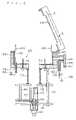
- FIGS. 1 and 2are side sectional views each showing the configuration of a heat treatment apparatus according to the present invention
- FIG. 3is a perspective view of a liner constituting the heat treatment apparatus shown in FIG. 1 ;
- FIG. 4is a partially enlarged view of the liner
- FIG. 5is a side sectional view of the heat treatment apparatus when the liner is to be detached.
- FIGS. 1 and 2are side sectional views each showing the configuration of a heat treatment apparatus according to the present invention which is intended for heat treatment of a substrate such as a semiconductor wafer by means of irradiation with flashlight emitted from a xenon flash lamp.
- the heat treatment apparatus of the present inventioncomprises a chamber 65 for heat treatment of a semiconductor wafer W stored therein.
- the chamber 65is formed by a translucent plate 61 , a base plate 62 , and a pair of side plates 63 and 64 .
- the translucent plate 61 as the upper portion of the chamber 65includes an infrared-transparent material such as quartz.
- the translucent plate 61is operative to function as a chamber window for allowing light emitted from a light source 5 to pass therethrough to be guided to the chamber 65 .
- the base plate 62 as the lower portion, and the side plates 63 and 64 as the side walls of the chamber 65include a metal material exhibiting excellence in strength and heat resistance such as stainless steel.
- Support pins 70are provided in an erect manner to the base plate 62 , penetrating a heat diffusion plate 73 and a hot plate 74 together constituting holding means of the semiconductor wafer W to be discussed later to support the semiconductor wafer W from the lower surface thereof.
- the side plate 64is provided with an opening 66 for transporting the semiconductor wafer W to and from the chamber 65 .
- a gate valve 68allows opening and closing of the opening 66 by its rotation about an axis 67 .
- the semiconductor wafer Wis transported to the chamber 65 by a transport robot not shown when the opening 66 is in an open state.
- the opening 66is brought to a closed state by the gate valve 68 when the semiconductor wafer W is to be subjected to heat treatment in the chamber 65 .
- the chamber 65is located below the light source 5 .
- the light source 5comprises more than one xenon flash lamp 69 (hereinafter also simply referred to as “flash lamp 69 ”), and a reflector 71 .
- the present preferred embodimentcomprises 25 xenon flash lamps 69 .
- the plurality of flash lamps 69are rod-shaped lamps each having an elongated cylindrical shape.
- the flash lamps 69are parallel to each other in an two-dimensional array, with the longitudinal directions each being in line with a horizontal direction.
- the reflector 71is located over the plurality of flash lamps 69 to be covered in their entirety.
- the xenon flash lamps 69each include a glass tube filled with xenon gas inside and having an anode and a cathode on both ends connected to a capacitor, and a trigger electrode wounded around the outer periphery of the glass tube.
- Xenon gasis an electrically insulating material, and thus in a normal state, does not allow electricity to flow in the glass tube.
- application of a high voltage to the trigger electrode for insulation breakdowncauses electricity stored in the capacitor to instantaneously flow into the glass tube, whereby resultant Joule heat is applied to xenon gas to cause light emission.
- each one of the xenon flash lamps 69electrostatic energy preliminarily stored therein is converted into extremely short light pulses ranging between 0.1 to 10 milliseconds. That is, the xenon flash lamps 69 characteristically emit light of considerably higher intensity as compared with a light source for continuous lightning.
- a light diffusion plate 72is interposed between the light source 5 and the translucent plate 61 .
- the light diffusion plate 72is a quartz glass member as an infrared-transparent material with a surface provided with a light diffusion property.
- Part of the light emitted from the flash lamps 69directly passes through the light diffusion plate 72 and the translucent plate 61 , then entering the chamber 65 .
- Other part of the light emitted from the flash lamps 69is reflected once by the reflector 71 , and thereafter, passes through the light diffusion plate 72 and the translucent plate 61 , then entering the chamber 65 .
- the chamber 65is provided therein with the hot plate 74 and the heat diffusion plate 73 .
- the heat diffusion plate 73is attached by adhesion on the upper surface of the hot plate 74 .
- Displacement preventing pins 75 for the semiconductor wafer Ware provided on the surface of the heat diffusion plate 73 .
- the hot plate 74serves to perform preheating (assist heating) of the semiconductor wafer W.
- the hot plate 74which is an aluminum nitride member, comprises therein a heater and a sensor for controlling the heater.
- the heat diffusion plate 73serves to diffuse heat energy from the hot plate 74 , thereby uniformly preheating and holding the semiconductor wafer W.
- the heat diffusion plate 73includes a low heat conductivity material such as sapphire (Al 2 O 3 ) or quartz.
- the wall surface of the chamber 65is fitted with a liner 20 .
- the liner 20is removably provided to the chamber 65 with no fixed relation therebetween.
- the wall surface of the chamber 65is defined as the inner wall surfaces of the side plates 63 and 64 , and the base plate 62 .
- the liner 20is a quartz member having a closed-end cylindrical shape that covers all the inner wall surfaces of the side plates 63 and 64 , and the base plate 62 . That is, the metal surface inside the chamber 65 is entirely covered with the liner 20 .
- FIG. 3is a perspective view of the liner 20 .
- the liner 20has a closed-end cylindrical shape comprising a tubular portion 20 a for covering the side plates 63 and 64 , and a base portion 20 b for covering the base plate 62 .
- the tubular portion 20 a and the base portion 20 bare separately formed and then joined. That is, the liner 20 is a divided member in which the tubular portion 20 a and the base portion 20 b are separable.
- the base portion 20 b of the liner 20is provided with a hole 22 for allowing upward and downward movement of a tubular member 41 , and through holes 21 for allowing the support pins 70 to pass therethrough. Though omitted from FIG.
- the hole 22 and the through holes 21are provided with annular portions in their perimeters slightly protruding in an upward direction.
- the tubular portion 20 ais provided with an opening 23 for allowing transportation of the semiconductor wafer W to and from the chamber 65 , and a passage (not shown) for allowing gas to pass therethrough which flows from an introduction path 78 toward a discharge path 79 .
- the liner 20is not limited to a divided member, but it may alternatively have a closed-end cylindrical shape molded in one piece.
- FIG. 4is a partially enlarged view of the liner 20 .
- An outer surface 2 a as part of the quartz surface of the liner 20 and facing the metal surface of the chamber 65 (that is, the inner wall surfaces of the side plates 63 and 64 , and of the base plate 62 )is subjected to honing for roughening.
- An inner surface 2 bis not subjected to honing, and thus, it has greater smoothness than the outer surface 2 a.
- honing as one of surface roughening techniquesincludes dry honing and wet honing.
- wet (liquid) honing for surface roughening of the outer surface 2 a of the liner 20the outer surface 2 a is sprayed at high speed with a liquid such as water that contains powdered abrasives (abrasive grains) kept in suspension therein.
- surface roughnessis adjusted by controlling conditions such as spray pressure and spray speed of a liquid, and the quantity, type, shape, size, hardness, the specific gravity, and concentration of suspension of abrasives.
- the outer surface 2 ais sprayed at high speed with abrasives by means of air.
- Surface roughnessis also adjusted in dry honing by controlling conditions such as spray pressure and spray speed of air, and the quantity, type, shape, size, hardness, and the specific gravity of abrasives.
- abrasivesmay be particles including silicon carbide, alumina, zirconia, stainless material, iron, glass beads, plastic, and the like.
- the outer surface 2 a of the liner 20is roughened by honing to have average surface roughness (Ra) of not less than 0.2 ⁇ m (preferably, not less than 1.6 ⁇ m).
- the inner surface 2 bhas greater smoothness than the outer surface 2 a (preferably, with average surface roughness (Ra) of not more than 6.3 ⁇ m).
- Both dry and wet honingprovide surface roughening to put a so-called satin finish on the outer surface 2 a of the liner 20 . Accordingly, when flashlight L emitted from the flash lamps 69 reaches the inner surface 2 b to enter the liner 20 , the outer surface 2 a after being subjected to surface roughening serves to scatter the flashlight L. As a result, the flashlight L does not outwardly exit from the outer surface 2 a . That is, the liner 20 is operative to serve as a light shield for blocking the light emitted from the flash lamps 69 from reaching the metal surface inside the chamber 65 . The metal surface inside the chamber 65 is entirely covered with the liner 20 as a light shield, and hence, the light emitted from the flash lamps 69 never reaches any part of this metal surface.
- a heat reflector 30is provided to surround the hot plate 74 , the heat diffusion plate 73 , and the tubular member 41 for supporting the plates 74 and 73 , except the upper surface of the heat diffusion plate 73 .
- the heat reflector 30is also a quartz member, and both surfaces thereof are further subjected to the foregoing honing process.
- the heat reflector 30serves to limit conduction of heat energy emitted from the hot plate 74 to the heat diffusion plate 73 .
- Actuation of a motor 40causes the heat diffusion plate 73 and the hot plate 74 to move up and down between the transportation position of the semiconductor wafer W shown in FIG. 1 and the heat treatment position of the semiconductor wafer W shown in FIG. 2 .
- the hot plate 74is coupled through the tubular member 41 to a moving plate 42 .
- the moving plate 42is guided through a guide member 43 suspended from the base plate 62 of the chamber 65 to be movable up and down.
- a fixed plate 44 fixed to the lower end of the guide member 43has a central portion where the motor 40 is provided to rotatably drive a ball screw 45 .
- the ball screw 45is threadedly engaged with a nut 48 that is coupled through coupling members 46 and 47 to the moving plate 42 .
- the heat diffusion plate 73 and the hot plate 74are thereby allowed to move up and down by means of actuation of the motor 40 between the transportation position of the semiconductor wafer W shown in FIG. 1 and the heat treatment position of the semiconductor wafer W shown in FIG. 2 . Upward and downward movement of the heat diffusion plate 73 and the hot plate 74 causes the heat reflector 30 provided above the moving plate 42 to move up and down.
- the heat diffusion plate 73 and the hot plate 74descend to the transportation position of the semiconductor wafer W shown in FIG. 1 for mounting the semiconductor wafer W on the support pins 70 that is transported through the opening 66 to the chamber 65 by means of a transport robot not shown, or for transporting the semiconductor wafer W mounted on the support pins 70 from the chamber 65 through the opening 66 .
- the upper ends of the support pins 70pass through the holes provided in the heat diffusion plate 73 and the hot plate 74 , protruding upward from the surface of the heat diffusion plate 73 .
- the heat diffusion plate 73 and the hot plate 74are elevated to the heat treatment position of the semiconductor wafer W shown in FIG. 2 which is higher than the upper ends of the support pins 70 .
- the semiconductor wafer W mounted on the support pins 70is transferred to the heat diffusion plate 73 .
- the transferred semiconductor wafer Wis elevated with the lower surface supported by the surface of the heat diffusion plate 73 , reaching a position close to the translucent plate 61 to be horizontally held thereat in the chamber 65 .
- the semiconductor wafer W supported on the heat diffusion plate 73is transferred to the support pins 70 .
- the translucent plate 61is interposed between the semiconductor wafer W supported on the heat diffusion plate 73 , the hot plate 74 , and the light source 5 .
- the heat diffusion plate 73 and the light source 5are allowed to have an arbitrary distance therebetween by controlling the amount of rotation of the motor 40 .
- Retractable bellows 77are provided between the base plate 62 of the chamber 65 and the moving plate 42 to surround the tubular member 41 , whereby the chamber 65 is hermetically sealed.
- the bellows 77are contracted when the heat diffusion plate 73 and the hot plate 74 are elevated to the heat treatment position, whereas the bellows 77 extend when the heat diffusion plate 73 and the hot plate 74 descend to the transportation position to isolate the atmosphere in the chamber 65 from an external atmosphere.
- the side plate 63 of the chamber 65 opposite to the opening 66is provided with the introduction path 78 cooperatively connected to an open/close valve 80 .
- the introduction path 78serves to introduce required process gas such as inert nitrogen gas into the chamber 65 .
- the opening 66 at the side plate 64is provided with the discharge path 79 cooperatively connected to an open/close valve 81 .
- the discharge path 79serves to discharge gas from the chamber 65 , and is connected through the open/close valve 81 to exhaust means not shown.
- the liner 20is provided with a passage for allowing gas to pass therethrough which flows from the introduction path 78 toward the discharge path 79 .
- the semiconductor wafer W to be subjected to heat treatment by this apparatusis an ion-implanted semiconductor wafer.
- the semiconductor wafer Wis transported through the opening 66 to the chamber 65 and is then mounted on the support pins 70 by means of a transport robot not shown.
- the opening 66is closed by the gate valve 68 .
- the motor 40is thereafter actuated to elevate the heat diffusion plate 73 and the hot plate 74 to the heat treatment position of the semiconductor wafer W shown in FIG. 2 , whereby the semiconductor wafer W is horizontally held thereat.
- the open/close valves 80 and 81are brought to an open state to produce a flow of nitrogen gas in the chamber 65 .
- the heat diffusion plate 73 and the hot plate 74are brought to a heated state by the heater stored in the hot plate 74 to a predetermined temperature.
- the semiconductor wafer Wis thus preheated by contacting the heat diffusion plate 73 in a heated state when the heat diffusion plate 73 and the hot plate 74 are elevated to the heat treatment position of the semiconductor wafer W, to cause gradual temperature rise of the semiconductor wafer W.
- the semiconductor wafer Wcontinues to be heated by the heat diffusion plate 73 .
- a temperature sensor not shownkeeps monitoring to determine whether the surface temperature of the semiconductor wafer W reaches a preheating temperature T 1 .
- the preheating temperature T 1is about 200 to 600° C. Temperature rise of the semiconductor wafer W to the preheating temperature T1 having such a range does not cause diffusion of ions implanted into the semiconductor wafer W.
- the flash lamps 69light up for flash heating, for a period of about 0.1 to 10 milliseconds.
- electrostatic energy preliminary storedis converted into light pulses of such an extremely short duration. That is, the flash lamps 69 emit light of considerably high intensity.
- the semiconductor wafer W subjected to such flash heatingexperiences instantaneous rise in surface temperature to a temperature T 2 of about 1000 to 1100° C. required for ion activation of the semiconductor wafer W.
- a temperature T 2of about 1000 to 1100° C. required for ion activation of the semiconductor wafer W.
- Rise of the surface temperature of the semiconductor wafer W to the processing temperature T 2 having such a rangecauses activation of ions implanted into the semiconductor wafer W.
- the semiconductor wafer Wis preheated by means of the hot plate 74 to rise its surface temperature to the preheating temperature T 1 of about 200 to 600° C. prior to lighting of the flash lamps 69 for heating the semiconductor wafer W.
- the semiconductor wafer Wis thereby allowed to rapidly rise in temperature to the processing temperature T 2 of about 1000 to 1100° C.
- the flashlight emitted from the flash lamps 69 of considerably high intensityis blocked by the outer surface 2 a of the liner 20 after being subjected to surface roughening by honing process, whereby the metal surface inside the chamber 65 is prevented from being exposed to the flashlight emitted from the flash lamps 69 .
- oxidation of metal as a result of flashlight irradiationis suppressed, to thereby prevent the metal surface in the chamber 65 from being coated with an oxide film.
- the metal surface inside the chamber 65is entirely covered with the liner 20 , and hence, the metal surface in the chamber 65 is prevented in its entirety from being coated with an oxide film as a result of flashlight irradiation.
- the motor 40is actuated to move down the heat diffusion plate 73 and the hot plate 74 to the transportation position of the semiconductor wafer W shown in FIG. 1 , and the gate valve 68 switches the opening 66 from a closed state to an open state. Further, the semiconductor wafer W mounted on the support pins 70 is transported from the chamber 65 by means of a transport robot not shown. Following the process described so far, a series of heat treatment operations is completed.
- the semiconductor wafer Wmay crack due to rapid thermal expansion of the wafer surface. Such cracking may cause the chamber 65 to be littered with fragments of the semiconductor wafer W.
- the liner 20is removably provided to the chamber 65 along the chamber wall surface. Even when the semiconductor wafer W cracks to litter the chamber 65 with its fragments, the chamber 65 can be easily cleaned by simply detaching the liner 20 from the chamber 65 . Smoothness of the inner surface 2 b of the liner 20 especially serves to promote cleaning of the liner 20 itself after detachment.
- the liner 20is detached from the chamber 65 .
- the light source 5 hingedly connected to the chamber 65is opened in an upward direction. Thereafter, the light diffusion plate 72 and the translucent plate 61 are removed.
- a screw which holds the tubular member 41 to the moving plate 42is unscrewed to remove the heat diffusion plate 73 , the hot plate 74 , and the tubular member 41 from the top opening of the chamber 65 .
- the heat reflector 30is also removed at this time from the top opening of the chamber 65 .
- the resultant stateis shown in FIG. 5 .
- the removable liner 20is thereafter detached from the chamber 65 .
- the foregoing detachment procedureis completely reversed.
- the present inventionis not limited to the preferred embodiment described so far.
- the number of the xenon flash lamps 69 provided to the light source 5is arbitrarily determined and is not limited to twenty five as in the foregoing preferred embodiment.
- the flash lamps 69are not limited to xenon flash lamps.
- the flash lamps 69may be krypton flash lamps.
- the light source 5may comprise another type of lamps (such as halogen lamps) instead of the flash lamps 69 to heat the semiconductor wafer W by means of irradiation of light emitted from these lamps.
- the technique according to the present inventionis also applicable to the heat treatment apparatus comprising such an alternative type of the light source 5 . That is, a chamber can be easily cleaned by removable provision of a quartz liner along the chamber wall surface. Further, a quartz liner after being subjected to honing process is provided along the inner wall surface of a chamber, which liner serves to block the light emitted from lamps from reaching the metal part of the wall surface inside the chamber. As a result, this metal part can be prevented from oxidation.
- the liner 20has the outer surface 2 a subjected to surface roughening by honing, and the inner surface 2 b having great smoothness.
- both surfaces of the liner 20may be subjected to surface roughening by honing.
- Such an alternativeimproves light blocking effect by the liner 20 , whereby the flashlight emitted from the flash lamps 69 can be blocked with higher reliability from reaching the metal surface inside the chamber 65 .
- the inner surface 2 b of the liner 20 having great smoothness as in the foregoing preferred embodimentserves to facilitate cleaning of the chamber 65 necessitated by cracking of the semiconductor wafer W during treatment, for example.
- a semiconductor waferis targeted for ion activation by means of light irradiation.
- a semiconductor waferis not a limited target for the processing by the heat treatment apparatus of the present invention.
- a glass substrateprovided with various types of silicon films thereon such as a silicon nitride film or a polycrystalline silicon film may be subjected to the processing by the heat treatment apparatus of the present invention.
- a polycrystalline silicon filmis provided by CVD on a glass substrate, and thereafter, this polycrystalline silicon film is subjected to ion implantation of silicon to be brought to an amorphous state.
- a silicon oxide filmis further provided as an antireflection film on the amorphous silicon film thereby formed.
- the heat treatment apparatus of the present inventionserves to emit light to the amorphous silicon film in its entirety, whereby the amorphous silicon film is switched to a polycrystalline state to form a polycrystalline silicon film.
- the heat treatment apparatus of the present inventionmay be directed to a TFT substrate comprising a glass substrate, and an underlying silicon oxide film and a polysilicon film as a crystallized film of amorphous silicon provided on the glass substrate, in which impurities such as phosphorous or boron are implanted into the polysilicon film.
- the heat treatment apparatus of the present inventionserves to emit light to the TFT substrate to activate the implanted impurities.
Landscapes
- Engineering & Computer Science (AREA)
- Physics & Mathematics (AREA)
- Condensed Matter Physics & Semiconductors (AREA)
- General Physics & Mathematics (AREA)
- Manufacturing & Machinery (AREA)
- Computer Hardware Design (AREA)
- Microelectronics & Electronic Packaging (AREA)
- Power Engineering (AREA)
- Mechanical Engineering (AREA)
- General Engineering & Computer Science (AREA)
- Health & Medical Sciences (AREA)
- Toxicology (AREA)
Abstract
Description
1. Field of the Invention
The present invention relates to a heat treatment apparatus for heat-treating a semiconductor wafer or a glass substrate (hereinafter simply referred to as a “substrate”) by means of light irradiation thereon.
2. Description of the Background Art
Conventional ion activation process of a semiconductor wafer after being subjected to ion implantation employs a heat treatment apparatus such as a lamp annealing apparatus using a halogen lamp. In such a heat treatment apparatus, a semiconductor wafer is heated up (annealed) to a temperature of about 1000 to 1100° C. to realize ion activation of the semiconductor wafer. Light energy emitted from the halogen lamp is operative to cause temperature rise of the wafer at a speed of about several hundreds of degrees centigrade per second.
An example of a lamp annealing apparatus using a halogen lamp is introduced in Japanese Patent Application Laid-Open No. 2001-127001, in which a metal surface in a processing chamber is covered with a coating material to suppress diffusion of metallic component from the metal surface during heat treatment.
Even in a heat treatment apparatus which realizes ion activation of a semiconductor wafer by means of temperature rise of the wafer at a speed of about several hundreds of degrees centigrade per second, ions implanted into the semiconductor wafer exhibit a rounded profile, which means ion diffusion by heat. Occurrence of this phenomenon necessitates implantation of ions in a greater amount than necessary, as the surface of the semiconductor wafer subjected to ion implantation with even high concentration experiences diffusion of the implanted ions therefrom.
In response, the surface of a semiconductor wafer is irradiated with flashlight by a xenon flash lamp, for example, so that only the surface of the semiconductor wafer implanted with ions is allowed to rise in temperature in a very short period of time of not longer than several milliseconds. An example of such a technique is introduced in Japanese Patent Application Laid-Open No. 59-169125 (1984) and No. 63-166219 (1988). Temperature rise in a very short period of time by use of a xenon flash lamp does not allow a period long enough for ion diffusion, thereby realizing ion activation with no rounding of a profile of ions implanted into a semiconductor wafer.
In a conventional heat treatment apparatus using a xenon flash lamp, a semiconductor wafer is contained in a stainless steel chamber, and the wafer surface is irradiated with flashlight. At this time, the inner wall of the chamber is also subjected to irradiation with flashlight emitted from the flash lamp.
The light emitted from the xenon flash lamp has considerably high intensity, which may result in generation of a brown oxide film during heat treatment that covers a metal surface inside the chamber. Even a slight source of contamination may result in imperfect treatment in light of recent trends toward high precision of a semiconductor device, for example. Generation of such an oxide film is thus unfavorable.
Necessity to minimize the source of contamination leading to particle contamination or metal contamination is not limited to an apparatus employing heating system by means of light irradiation, but is common to a conventional heat treatment apparatus for a semiconductor device, for example. Japanese Patent Application Laid-Open No. 2002-60926 suggests a cleaning technique responsive thereto, in which a deposited material adhered to a component in a heat treatment chamber, for example, is heated to sublimate. Another cleaning technique includes removal of a product of the decomposition of source gas adhered to a heat treatment chamber by means of heat treatment in an atmosphere such as halogen gas, an example of which is suggested in Japanese Patent Application Laid-Open No. 2002-313727.
In addition to the foregoing adherence of a deposited material, contamination of a heat treatment chamber results from various reasons. By way of example, a semiconductor wafer under treatment may crack, causing a treatment chamber to be littered with the fragments thereof. Especially in a heat treatment apparatus using a xenon flash lamp, a semiconductor wafer is instantaneously irradiated with considerably high-energy light, thereby causing rapid temperature rise of the surface of the semiconductor wafer in a moment. As a result, the semiconductor wafer may crack due to rapid thermal expansion of the surface.
The resultant fragments of the semiconductor wafer cannot be removed by heat treatment, for example. The treatment chamber should be opened for mechanically cleaning the inside. However, a heat treatment chamber with a complicated configuration cannot be easily cleaned, imposing difficulty in completely removing the source of pollution such as fragments of a semiconductor wafer.
The present invention is directed to a heat treatment apparatus for irradiating a substrate with light to heat the substrate.
According to the present invention, the heat treatment apparatus comprises a light source having a plurality of flash lamps, a chamber provided below the light source, a holding member for holding a substrate in the chamber, and a light shield provided in the chamber, the light shield blocking light emitted from the light source from reaching a metal surface inside the chamber.
The metal surface inside the chamber is prevented from being exposed to the flashlight emitted from the flash lamps. As a result, oxidation of the metal surface as a result of flashlight irradiation is suppressed, to thereby prevent the metal surface inside the chamber from being coated with an oxide film during heat treatment.
According to another aspect of the present invention, the heat treatment apparatus comprises a light source having a plurality of lamps, a chamber provided below the light source, a holding member for holding a substrate in a substantially horizontal position in the chamber, and a liner removably provided to the chamber along a wall surface of the chamber.
When the substrate cracks to litter the chamber with its fragments, the chamber can be easily cleaned by simply detaching the liner from the chamber.
It is therefore an object of the present invention to provide a heat treatment apparatus capable of preventing a metal surface inside a chamber from being coated with an oxide film during heat treatment.
It is another object of the present invention to provide a heat treatment apparatus capable of easily cleaning a chamber.
These and other objects, features, aspects and advantages of the present invention will become more apparent from the following detailed description of the present invention when taken in conjunction with the accompanying drawings.
The preferred embodiment of the present invention will be described in detail with reference to the drawings.
The heat treatment apparatus of the present invention comprises achamber 65 for heat treatment of a semiconductor wafer W stored therein. Thechamber 65 is formed by atranslucent plate 61, abase plate 62, and a pair ofside plates translucent plate 61 as the upper portion of thechamber 65 includes an infrared-transparent material such as quartz. Thetranslucent plate 61 is operative to function as a chamber window for allowing light emitted from alight source 5 to pass therethrough to be guided to thechamber 65. As an example, thebase plate 62 as the lower portion, and theside plates chamber 65, include a metal material exhibiting excellence in strength and heat resistance such as stainless steel.
Thechamber 65 is located below thelight source 5. Thelight source 5 comprises more than one xenon flash lamp69 (hereinafter also simply referred to as “flash lamp 69”), and areflector 71. The present preferred embodiment comprises 25xenon flash lamps 69. The plurality offlash lamps 69 are rod-shaped lamps each having an elongated cylindrical shape. Theflash lamps 69 are parallel to each other in an two-dimensional array, with the longitudinal directions each being in line with a horizontal direction. Thereflector 71 is located over the plurality offlash lamps 69 to be covered in their entirety.
Thexenon flash lamps 69 each include a glass tube filled with xenon gas inside and having an anode and a cathode on both ends connected to a capacitor, and a trigger electrode wounded around the outer periphery of the glass tube. Xenon gas is an electrically insulating material, and thus in a normal state, does not allow electricity to flow in the glass tube. However, application of a high voltage to the trigger electrode for insulation breakdown causes electricity stored in the capacitor to instantaneously flow into the glass tube, whereby resultant Joule heat is applied to xenon gas to cause light emission. In each one of thexenon flash lamps 69, electrostatic energy preliminarily stored therein is converted into extremely short light pulses ranging between 0.1 to 10 milliseconds. That is, thexenon flash lamps 69 characteristically emit light of considerably higher intensity as compared with a light source for continuous lightning.
Alight diffusion plate 72 is interposed between thelight source 5 and thetranslucent plate 61. Thelight diffusion plate 72 is a quartz glass member as an infrared-transparent material with a surface provided with a light diffusion property.
Part of the light emitted from theflash lamps 69 directly passes through thelight diffusion plate 72 and thetranslucent plate 61, then entering thechamber 65. Other part of the light emitted from theflash lamps 69 is reflected once by thereflector 71, and thereafter, passes through thelight diffusion plate 72 and thetranslucent plate 61, then entering thechamber 65.
Thechamber 65 is provided therein with thehot plate 74 and theheat diffusion plate 73. Theheat diffusion plate 73 is attached by adhesion on the upper surface of thehot plate 74. Displacement preventing pins75 for the semiconductor wafer W are provided on the surface of theheat diffusion plate 73.
Thehot plate 74 serves to perform preheating (assist heating) of the semiconductor wafer W. Thehot plate 74, which is an aluminum nitride member, comprises therein a heater and a sensor for controlling the heater. Theheat diffusion plate 73 serves to diffuse heat energy from thehot plate 74, thereby uniformly preheating and holding the semiconductor wafer W. Theheat diffusion plate 73 includes a low heat conductivity material such as sapphire (Al2O3) or quartz.
The wall surface of thechamber 65 is fitted with aliner 20. Theliner 20 is removably provided to thechamber 65 with no fixed relation therebetween. The wall surface of thechamber 65 is defined as the inner wall surfaces of theside plates base plate 62. As an example, theliner 20 is a quartz member having a closed-end cylindrical shape that covers all the inner wall surfaces of theside plates base plate 62. That is, the metal surface inside thechamber 65 is entirely covered with theliner 20.
In the present preferred embodiment, honing as one of surface roughening techniques includes dry honing and wet honing. In wet (liquid) honing for surface roughening of the outer surface2aof theliner 20, the outer surface2ais sprayed at high speed with a liquid such as water that contains powdered abrasives (abrasive grains) kept in suspension therein. In wet honing, surface roughness is adjusted by controlling conditions such as spray pressure and spray speed of a liquid, and the quantity, type, shape, size, hardness, the specific gravity, and concentration of suspension of abrasives.
In dry honing for surface roughening of the outer surface2aof theliner 20, the outer surface2ais sprayed at high speed with abrasives by means of air. Surface roughness is also adjusted in dry honing by controlling conditions such as spray pressure and spray speed of air, and the quantity, type, shape, size, hardness, and the specific gravity of abrasives.
In either honing, abrasives may be particles including silicon carbide, alumina, zirconia, stainless material, iron, glass beads, plastic, and the like. In the present preferred embodiment, the outer surface2aof theliner 20 is roughened by honing to have average surface roughness (Ra) of not less than 0.2 μm (preferably, not less than 1.6 μm). Theinner surface 2bhas greater smoothness than the outer surface2a(preferably, with average surface roughness (Ra) of not more than 6.3 μm).
Both dry and wet honing provide surface roughening to put a so-called satin finish on the outer surface2aof theliner 20. Accordingly, when flashlight L emitted from theflash lamps 69 reaches theinner surface 2bto enter theliner 20, the outer surface2aafter being subjected to surface roughening serves to scatter the flashlight L. As a result, the flashlight L does not outwardly exit from the outer surface2a. That is, theliner 20 is operative to serve as a light shield for blocking the light emitted from theflash lamps 69 from reaching the metal surface inside thechamber 65. The metal surface inside thechamber 65 is entirely covered with theliner 20 as a light shield, and hence, the light emitted from theflash lamps 69 never reaches any part of this metal surface.
Aheat reflector 30 is provided to surround thehot plate 74, theheat diffusion plate 73, and thetubular member 41 for supporting theplates heat diffusion plate 73. Theheat reflector 30 is also a quartz member, and both surfaces thereof are further subjected to the foregoing honing process. Theheat reflector 30 serves to limit conduction of heat energy emitted from thehot plate 74 to theheat diffusion plate 73.
Actuation of amotor 40 causes theheat diffusion plate 73 and thehot plate 74 to move up and down between the transportation position of the semiconductor wafer W shown inFIG. 1 and the heat treatment position of the semiconductor wafer W shown inFIG. 2 .
Thehot plate 74 is coupled through thetubular member 41 to a movingplate 42. The movingplate 42 is guided through aguide member 43 suspended from thebase plate 62 of thechamber 65 to be movable up and down. A fixedplate 44 fixed to the lower end of theguide member 43 has a central portion where themotor 40 is provided to rotatably drive aball screw 45. The ball screw45 is threadedly engaged with anut 48 that is coupled throughcoupling members plate 42. Theheat diffusion plate 73 and thehot plate 74 are thereby allowed to move up and down by means of actuation of themotor 40 between the transportation position of the semiconductor wafer W shown inFIG. 1 and the heat treatment position of the semiconductor wafer W shown inFIG. 2 . Upward and downward movement of theheat diffusion plate 73 and thehot plate 74 causes theheat reflector 30 provided above the movingplate 42 to move up and down.
Theheat diffusion plate 73 and thehot plate 74 descend to the transportation position of the semiconductor wafer W shown inFIG. 1 for mounting the semiconductor wafer W on the support pins70 that is transported through theopening 66 to thechamber 65 by means of a transport robot not shown, or for transporting the semiconductor wafer W mounted on the support pins70 from thechamber 65 through theopening 66. In the state ofFIG. 1 , the upper ends of the support pins70 pass through the holes provided in theheat diffusion plate 73 and thehot plate 74, protruding upward from the surface of theheat diffusion plate 73.
For heat treatment of the semiconductor wafer W, theheat diffusion plate 73 and thehot plate 74 are elevated to the heat treatment position of the semiconductor wafer W shown inFIG. 2 which is higher than the upper ends of the support pins70. In the process of moving up theheat diffusion plate 73 and thehot plate 74 from the transportation position ofFIG. 1 to the heat treatment position ofFIG. 2 , the semiconductor wafer W mounted on the support pins70 is transferred to theheat diffusion plate 73. The transferred semiconductor wafer W is elevated with the lower surface supported by the surface of theheat diffusion plate 73, reaching a position close to thetranslucent plate 61 to be horizontally held thereat in thechamber 65. Conversely, in the process of moving down theheat diffusion plate 73 and thehot plate 74 from the heat treatment position ofFIG. 2 to the transportation position ofFIG. 1 , the semiconductor wafer W supported on theheat diffusion plate 73 is transferred to the support pins70.
When theheat diffusion plate 73 and thehot plate 74 for supporting the semiconductor wafer W are held at the heat treatment position, thetranslucent plate 61 is interposed between the semiconductor wafer W supported on theheat diffusion plate 73, thehot plate 74, and thelight source 5. Theheat diffusion plate 73 and thelight source 5 are allowed to have an arbitrary distance therebetween by controlling the amount of rotation of themotor 40.
Retractable bellows77 are provided between thebase plate 62 of thechamber 65 and the movingplate 42 to surround thetubular member 41, whereby thechamber 65 is hermetically sealed. The bellows77 are contracted when theheat diffusion plate 73 and thehot plate 74 are elevated to the heat treatment position, whereas thebellows 77 extend when theheat diffusion plate 73 and thehot plate 74 descend to the transportation position to isolate the atmosphere in thechamber 65 from an external atmosphere.
Theside plate 63 of thechamber 65 opposite to theopening 66 is provided with theintroduction path 78 cooperatively connected to an open/close valve 80. Theintroduction path 78 serves to introduce required process gas such as inert nitrogen gas into thechamber 65. Theopening 66 at theside plate 64 is provided with thedischarge path 79 cooperatively connected to an open/close valve 81. Thedischarge path 79 serves to discharge gas from thechamber 65, and is connected through the open/close valve 81 to exhaust means not shown. Theliner 20 is provided with a passage for allowing gas to pass therethrough which flows from theintroduction path 78 toward thedischarge path 79.
Next, it will be discussed how the heat treatment apparatus having the foregoing configuration performs heat treatment of the semiconductor wafer W. The semiconductor wafer W to be subjected to heat treatment by this apparatus is an ion-implanted semiconductor wafer.
When theheat diffusion plate 73 and thehot plate 74 are at the transportation position of the semiconductor wafer W shown inFIG. 1 , the semiconductor wafer W is transported through theopening 66 to thechamber 65 and is then mounted on the support pins70 by means of a transport robot not shown. When transportation of the semiconductor wafer W to thechamber 65 is finished, theopening 66 is closed by thegate valve 68. Themotor 40 is thereafter actuated to elevate theheat diffusion plate 73 and thehot plate 74 to the heat treatment position of the semiconductor wafer W shown inFIG. 2 , whereby the semiconductor wafer W is horizontally held thereat. Further, the open/close valves chamber 65.
Theheat diffusion plate 73 and thehot plate 74 are brought to a heated state by the heater stored in thehot plate 74 to a predetermined temperature. The semiconductor wafer W is thus preheated by contacting theheat diffusion plate 73 in a heated state when theheat diffusion plate 73 and thehot plate 74 are elevated to the heat treatment position of the semiconductor wafer W, to cause gradual temperature rise of the semiconductor wafer W.
The semiconductor wafer W continues to be heated by theheat diffusion plate 73. When temperature rise of the semiconductor wafer W occurs, a temperature sensor not shown keeps monitoring to determine whether the surface temperature of the semiconductor wafer W reaches a preheating temperature T1.
As an example, the preheating temperature T1 is about 200 to 600° C. Temperature rise of the semiconductor wafer W to the preheating temperature T1 having such a range does not cause diffusion of ions implanted into the semiconductor wafer W.
At the time when the surface temperature of the semiconductor wafer W reaches the preheating temperature T1, theflash lamps 69 light up for flash heating, for a period of about 0.1 to 10 milliseconds. In each one of theflash lamps 69, electrostatic energy preliminary stored is converted into light pulses of such an extremely short duration. That is, theflash lamps 69 emit light of considerably high intensity.
The semiconductor wafer W subjected to such flash heating experiences instantaneous rise in surface temperature to a temperature T2 of about 1000 to 1100° C. required for ion activation of the semiconductor wafer W. Rise of the surface temperature of the semiconductor wafer W to the processing temperature T2 having such a range causes activation of ions implanted into the semiconductor wafer W.
Rise of the surface temperature of the semiconductor wafer W to the processing temperature T2 requires a very short period of about 0.1 to 10 milliseconds, and hence, activation of ions implanted into the semiconductor wafer W is completed in a short period. As a result, no diffusion of ions implanted into the semiconductor wafer W occurs, thereby preventing rounding of a profile of ions implanted into the semiconductor wafer W. Ion activation requires a period of time considerably shorter than a period required for ion diffusion, and hence, ion activation is completed even in a short period of about 0.1 to 10 milliseconds that causes no ion diffusion.
The semiconductor wafer W is preheated by means of thehot plate 74 to rise its surface temperature to the preheating temperature T1 of about 200 to 600° C. prior to lighting of theflash lamps 69 for heating the semiconductor wafer W. The semiconductor wafer W is thereby allowed to rapidly rise in temperature to the processing temperature T2 of about 1000 to 1100° C.
The flashlight emitted from theflash lamps 69 of considerably high intensity is blocked by the outer surface2aof theliner 20 after being subjected to surface roughening by honing process, whereby the metal surface inside thechamber 65 is prevented from being exposed to the flashlight emitted from theflash lamps 69. As a result, oxidation of metal as a result of flashlight irradiation is suppressed, to thereby prevent the metal surface in thechamber 65 from being coated with an oxide film.
Especially in the present preferred embodiment, the metal surface inside thechamber 65 is entirely covered with theliner 20, and hence, the metal surface in thechamber 65 is prevented in its entirety from being coated with an oxide film as a result of flashlight irradiation.
After flash heating, themotor 40 is actuated to move down theheat diffusion plate 73 and thehot plate 74 to the transportation position of the semiconductor wafer W shown inFIG. 1 , and thegate valve 68 switches the opening66 from a closed state to an open state. Further, the semiconductor wafer W mounted on the support pins70 is transported from thechamber 65 by means of a transport robot not shown. Following the process described so far, a series of heat treatment operations is completed.
As discussed, in the process of heating the semiconductor wafer W by lighting theflash lamps 69, the semiconductor wafer W may crack due to rapid thermal expansion of the wafer surface. Such cracking may cause thechamber 65 to be littered with fragments of the semiconductor wafer W.
In the present preferred embodiment, theliner 20 is removably provided to thechamber 65 along the chamber wall surface. Even when the semiconductor wafer W cracks to litter thechamber 65 with its fragments, thechamber 65 can be easily cleaned by simply detaching theliner 20 from thechamber 65. Smoothness of theinner surface 2bof theliner 20 especially serves to promote cleaning of theliner 20 itself after detachment.
Next, it will be discussed how theliner 20 is detached from thechamber 65. Thelight source 5 hingedly connected to thechamber 65 is opened in an upward direction. Thereafter, thelight diffusion plate 72 and thetranslucent plate 61 are removed. Next, a screw which holds thetubular member 41 to the movingplate 42 is unscrewed to remove theheat diffusion plate 73, thehot plate 74, and thetubular member 41 from the top opening of thechamber 65. Theheat reflector 30 is also removed at this time from the top opening of thechamber 65. The resultant state is shown inFIG. 5 .
As indicated by an arrow AR4 ofFIG. 5 , theremovable liner 20 is thereafter detached from thechamber 65. When cleaning is finished and theliner 20 is to return to its position, the foregoing detachment procedure is completely reversed.
The present invention is not limited to the preferred embodiment described so far. As an example, the number of thexenon flash lamps 69 provided to thelight source 5 is arbitrarily determined and is not limited to twenty five as in the foregoing preferred embodiment. Further, theflash lamps 69 are not limited to xenon flash lamps. As an example, theflash lamps 69 may be krypton flash lamps.
Thelight source 5 may comprise another type of lamps (such as halogen lamps) instead of theflash lamps 69 to heat the semiconductor wafer W by means of irradiation of light emitted from these lamps. The technique according to the present invention is also applicable to the heat treatment apparatus comprising such an alternative type of thelight source 5. That is, a chamber can be easily cleaned by removable provision of a quartz liner along the chamber wall surface. Further, a quartz liner after being subjected to honing process is provided along the inner wall surface of a chamber, which liner serves to block the light emitted from lamps from reaching the metal part of the wall surface inside the chamber. As a result, this metal part can be prevented from oxidation.
In the preferred embodiment described above, theliner 20 has the outer surface2asubjected to surface roughening by honing, and theinner surface 2bhaving great smoothness. Alternatively, both surfaces of theliner 20 may be subjected to surface roughening by honing. Such an alternative improves light blocking effect by theliner 20, whereby the flashlight emitted from theflash lamps 69 can be blocked with higher reliability from reaching the metal surface inside thechamber 65. However, theinner surface 2bof theliner 20 having great smoothness as in the foregoing preferred embodiment serves to facilitate cleaning of thechamber 65 necessitated by cracking of the semiconductor wafer W during treatment, for example.
In the preferred embodiment described above, a semiconductor wafer is targeted for ion activation by means of light irradiation. However, a semiconductor wafer is not a limited target for the processing by the heat treatment apparatus of the present invention. As an example, a glass substrate provided with various types of silicon films thereon such as a silicon nitride film or a polycrystalline silicon film may be subjected to the processing by the heat treatment apparatus of the present invention. More particularly, a polycrystalline silicon film is provided by CVD on a glass substrate, and thereafter, this polycrystalline silicon film is subjected to ion implantation of silicon to be brought to an amorphous state. A silicon oxide film is further provided as an antireflection film on the amorphous silicon film thereby formed. In this state, the heat treatment apparatus of the present invention serves to emit light to the amorphous silicon film in its entirety, whereby the amorphous silicon film is switched to a polycrystalline state to form a polycrystalline silicon film.
Further alternatively, the heat treatment apparatus of the present invention may be directed to a TFT substrate comprising a glass substrate, and an underlying silicon oxide film and a polysilicon film as a crystallized film of amorphous silicon provided on the glass substrate, in which impurities such as phosphorous or boron are implanted into the polysilicon film. In this case, the heat treatment apparatus of the present invention serves to emit light to the TFT substrate to activate the implanted impurities.
While the invention has been shown and described in detail, the foregoing description is in all aspects illustrative and not restrictive. It is therefore understood that numerous modifications and variations can be devised without departing from the scope of the invention.
Claims (18)
1. A heat treatment apparatus for irradiating a substrate with flashlight to heat said substrate, comprising:
a light source having a plurality of flash lamps;
a chamber provided below said light source;
a holding member for holding a substrate in said chamber; and
a light shield provided in said chamber, said light shield blocking light emitted from said light source from reaching a metal surface inside said chamber,
wherein said light shield is a quartz member with a quartz surface roughened by honing.
2. The heat treatment apparatus according toclaim 1 ,
wherein said chamber has a metallic side plate and a metallic bottom plate; and
wherein said light shield has a closed-end cylindrical shape for covering inner wall surfaces of said side plate and said bottom plate.
3. The heat treatment apparatus according toclaim 2 ,
wherein said light shield is a divided member in which a tubular portion and a base portion are separable.
4. The heat treatment apparatus according toclaim 3 ,
wherein said light shield covers said metal surface inside said chamber in its entirety.
5. The heat treatment apparatus according toclaim 4 ,
wherein said quartz surface has an outer surface and an inner surface, said outer surface facing said metal surface inside said chamber and being roughed by honing, said inner surface having greater smoothness than said outer surface.
6. The heat treatment apparatus according toclaim 5 ,
wherein said outer surface has average surface roughness of not less than 0.2 μm.
7. A heat treatment apparatus for irradiating a substrate with flashlight to heat said substrate, comprising:
a light source having a plurality of flash lamps;
a chamber provided below said light source;
a holding member for holding a substrate in a substantially horizontal position in said chamber; and
a liner removably provided at said chamber, along an inner wall side surface and an inner wall base surface of said chamber to cover said side and base surfaces, said liner having a roughened outer surface facing said side and base surfaces of said chamber and an inner surface having greater smoothness than said outer surface.
8. The heat treatment apparatus according toclaim 7 ,
wherein said liner has a closed-end cylindrical shape.
9. The heat treatment apparatus according toclaim 8 ,
wherein said liner is a divided member in which a tubular portion and a base portion are separable.
10. The heat treatment apparatus according toclaim 9 ,
wherein said liner is quartz member.
11. A heat treatment apparatus for irradiating a substrate with flashlight to heat said substrate, comprising:
a light source having a plurality of flash lamps;
a chamber provided below said light source:
a holding member for holding a substrate in said chamber; and
a light shield provided in said chamber, said light shield blocking light emitted from said light source from reaching a metal surface inside said chamber,
wherein said light shield has a roughened outer surface and an inner surface having greater smoothness than said outer surface.
12. The heat treatment apparatus according toclaim 11 ,
wherein said chamber has a metallic side plate and a metallic bottom plate; and
wherein said light shield has a closed-end cylindrical shape for covering inner wall surfaces of said side plate and said bottom plate.
13. The heat treatment apparatus according toclaim 12 ,
wherein said light shield is a divided member in which a tubular portion and a base portion are separable.
14. The heat treatment apparatus according toclaim 13 ,
wherein said light shield covers said metal surface inside said chamber in its entirety.
15. The heat treatment apparatus according toclaim 14 ,
wherein said outer surface has average surface roughness of not less than 0.2 μm.
16. A heat treatment apparatus for irradiating a substrate with flashlight to heat said substrate, comprising:
a light source having a plurality of flash lamps;
a chamber provided below said light source;
a holding member for holding a substrate in a substantially horizontal position in said chamber; and
a liner removably provided at said chamber, along an inner wall side surface and an inner wall base surface of said chamber to cover said side and base surfaces,
wherein said liner is a quartz member with a quartz surface roughened by honing.
17. The heat treatment apparatus according toclaim 16 ,
wherein said liner has a closed-end cylindrical shape.
18. The heat treatment apparatus according toclaim 17 ,
wherein said liner is a divided member in which a tubular portion and a base portion are separable.
Applications Claiming Priority (4)
| Application Number | Priority Date | Filing Date | Title |
|---|---|---|---|
| JP2003050896AJP4417017B2 (en) | 2003-02-27 | 2003-02-27 | Heat treatment equipment |
| JP2003-050896 | 2003-02-27 | ||
| JP2003-114036 | 2003-04-18 | ||
| JP2003114036AJP4417023B2 (en) | 2003-04-18 | 2003-04-18 | Heat treatment equipment |
Publications (2)
| Publication Number | Publication Date |
|---|---|
| US20040169032A1 US20040169032A1 (en) | 2004-09-02 |
| US7091453B2true US7091453B2 (en) | 2006-08-15 |
Family
ID=32911443
Family Applications (1)
| Application Number | Title | Priority Date | Filing Date |
|---|---|---|---|
| US10/780,420Expired - LifetimeUS7091453B2 (en) | 2003-02-27 | 2004-02-17 | Heat treatment apparatus by means of light irradiation |
Country Status (2)
| Country | Link |
|---|---|
| US (1) | US7091453B2 (en) |
| KR (1) | KR100582934B1 (en) |
Cited By (12)
| Publication number | Priority date | Publication date | Assignee | Title |
|---|---|---|---|---|
| US20060291835A1 (en)* | 2005-06-23 | 2006-12-28 | Dainippon Screen Mfg., Co., Ltd. | Susceptor for heat treatment and heat treatment apparatus |
| US20100151695A1 (en)* | 2008-12-15 | 2010-06-17 | Canon Anelva Corporation | Substrate processing apparatus, substrate annealing method, and semiconductor device manufacturing method |
| US20110117753A1 (en)* | 2009-08-04 | 2011-05-19 | C/O Canon Anelva Corporation | Heat treatment apparatus and semiconductor device manufacturing method |
| US20110143297A1 (en)* | 2011-01-28 | 2011-06-16 | Poole Ventura, Inc. | Thermal Diffusion Chamber |
| US20110249960A1 (en)* | 2011-01-28 | 2011-10-13 | Poole Ventura, Inc. | Heat Source Door For A Thermal Diffusion Chamber |
| US20120161405A1 (en)* | 2010-12-20 | 2012-06-28 | Mohn Jonathan D | System and apparatus for flowable deposition in semiconductor fabrication |
| US20140345526A1 (en)* | 2013-05-23 | 2014-11-27 | Applied Materials, Inc. | Coated liner assembly for a semiconductor processing chamber |
| US8950470B2 (en) | 2010-12-30 | 2015-02-10 | Poole Ventura, Inc. | Thermal diffusion chamber control device and method |
| US9847222B2 (en) | 2013-10-25 | 2017-12-19 | Lam Research Corporation | Treatment for flowable dielectric deposition on substrate surfaces |
| US9916977B2 (en) | 2015-11-16 | 2018-03-13 | Lam Research Corporation | Low k dielectric deposition via UV driven photopolymerization |
| US10049921B2 (en) | 2014-08-20 | 2018-08-14 | Lam Research Corporation | Method for selectively sealing ultra low-k porous dielectric layer using flowable dielectric film formed from vapor phase dielectric precursor |
| US10388546B2 (en) | 2015-11-16 | 2019-08-20 | Lam Research Corporation | Apparatus for UV flowable dielectric |
Families Citing this family (409)
| Publication number | Priority date | Publication date | Assignee | Title |
|---|---|---|---|---|
| US8986456B2 (en) | 2006-10-10 | 2015-03-24 | Asm America, Inc. | Precursor delivery system |
| DE102007058002B4 (en)* | 2007-12-03 | 2016-03-17 | Mattson Thermal Products Gmbh | Device for the thermal treatment of disc-shaped semiconductor substrates |
| US10378106B2 (en) | 2008-11-14 | 2019-08-13 | Asm Ip Holding B.V. | Method of forming insulation film by modified PEALD |
| US9394608B2 (en) | 2009-04-06 | 2016-07-19 | Asm America, Inc. | Semiconductor processing reactor and components thereof |
| US8883270B2 (en) | 2009-08-14 | 2014-11-11 | Asm America, Inc. | Systems and methods for thin-film deposition of metal oxides using excited nitrogen—oxygen species |
| US8877655B2 (en) | 2010-05-07 | 2014-11-04 | Asm America, Inc. | Systems and methods for thin-film deposition of metal oxides using excited nitrogen-oxygen species |
| US8802201B2 (en) | 2009-08-14 | 2014-08-12 | Asm America, Inc. | Systems and methods for thin-film deposition of metal oxides using excited nitrogen-oxygen species |
| JP5507274B2 (en)* | 2010-01-29 | 2014-05-28 | 大日本スクリーン製造株式会社 | Heat treatment method and heat treatment apparatus |
| US9312155B2 (en) | 2011-06-06 | 2016-04-12 | Asm Japan K.K. | High-throughput semiconductor-processing apparatus equipped with multiple dual-chamber modules |
| US9793148B2 (en) | 2011-06-22 | 2017-10-17 | Asm Japan K.K. | Method for positioning wafers in multiple wafer transport |
| US10364496B2 (en) | 2011-06-27 | 2019-07-30 | Asm Ip Holding B.V. | Dual section module having shared and unshared mass flow controllers |
| US10854498B2 (en) | 2011-07-15 | 2020-12-01 | Asm Ip Holding B.V. | Wafer-supporting device and method for producing same |
| US20130023129A1 (en) | 2011-07-20 | 2013-01-24 | Asm America, Inc. | Pressure transmitter for a semiconductor processing environment |
| WO2013023092A2 (en)* | 2011-08-10 | 2013-02-14 | Applied Materials, Inc | Robot systems, apparatus, and methods adapted to process substrates in multiple tiers |
| KR101894089B1 (en)* | 2011-10-24 | 2018-08-31 | 엘지디스플레이 주식회사 | Manufacturing Method of Flexible Display Device |
| US9341296B2 (en) | 2011-10-27 | 2016-05-17 | Asm America, Inc. | Heater jacket for a fluid line |
| US9096931B2 (en) | 2011-10-27 | 2015-08-04 | Asm America, Inc | Deposition valve assembly and method of heating the same |
| US9017481B1 (en) | 2011-10-28 | 2015-04-28 | Asm America, Inc. | Process feed management for semiconductor substrate processing |
| US9005539B2 (en) | 2011-11-23 | 2015-04-14 | Asm Ip Holding B.V. | Chamber sealing member |
| US9167625B2 (en)* | 2011-11-23 | 2015-10-20 | Asm Ip Holding B.V. | Radiation shielding for a substrate holder |
| US9202727B2 (en) | 2012-03-02 | 2015-12-01 | ASM IP Holding | Susceptor heater shim |
| US8946830B2 (en) | 2012-04-04 | 2015-02-03 | Asm Ip Holdings B.V. | Metal oxide protective layer for a semiconductor device |
| TWI622664B (en) | 2012-05-02 | 2018-05-01 | Asm智慧財產控股公司 | Phase stable film, structure and device comprising the same, and method of forming same |
| US8728832B2 (en) | 2012-05-07 | 2014-05-20 | Asm Ip Holdings B.V. | Semiconductor device dielectric interface layer |
| US8933375B2 (en) | 2012-06-27 | 2015-01-13 | Asm Ip Holding B.V. | Susceptor heater and method of heating a substrate |
| US9558931B2 (en) | 2012-07-27 | 2017-01-31 | Asm Ip Holding B.V. | System and method for gas-phase sulfur passivation of a semiconductor surface |
| US9117866B2 (en) | 2012-07-31 | 2015-08-25 | Asm Ip Holding B.V. | Apparatus and method for calculating a wafer position in a processing chamber under process conditions |
| US9169975B2 (en) | 2012-08-28 | 2015-10-27 | Asm Ip Holding B.V. | Systems and methods for mass flow controller verification |
| US9659799B2 (en) | 2012-08-28 | 2017-05-23 | Asm Ip Holding B.V. | Systems and methods for dynamic semiconductor process scheduling |
| US9021985B2 (en) | 2012-09-12 | 2015-05-05 | Asm Ip Holdings B.V. | Process gas management for an inductively-coupled plasma deposition reactor |
| US9324811B2 (en) | 2012-09-26 | 2016-04-26 | Asm Ip Holding B.V. | Structures and devices including a tensile-stressed silicon arsenic layer and methods of forming same |
| US10714315B2 (en) | 2012-10-12 | 2020-07-14 | Asm Ip Holdings B.V. | Semiconductor reaction chamber showerhead |
| US9640416B2 (en) | 2012-12-26 | 2017-05-02 | Asm Ip Holding B.V. | Single-and dual-chamber module-attachable wafer-handling chamber |
| US20160376700A1 (en) | 2013-02-01 | 2016-12-29 | Asm Ip Holding B.V. | System for treatment of deposition reactor |
| US8894870B2 (en) | 2013-02-01 | 2014-11-25 | Asm Ip Holding B.V. | Multi-step method and apparatus for etching compounds containing a metal |
| US9484191B2 (en) | 2013-03-08 | 2016-11-01 | Asm Ip Holding B.V. | Pulsed remote plasma method and system |
| US9589770B2 (en) | 2013-03-08 | 2017-03-07 | Asm Ip Holding B.V. | Method and systems for in-situ formation of intermediate reactive species |
| US8993054B2 (en) | 2013-07-12 | 2015-03-31 | Asm Ip Holding B.V. | Method and system to reduce outgassing in a reaction chamber |
| US9018111B2 (en) | 2013-07-22 | 2015-04-28 | Asm Ip Holding B.V. | Semiconductor reaction chamber with plasma capabilities |
| US9396934B2 (en) | 2013-08-14 | 2016-07-19 | Asm Ip Holding B.V. | Methods of forming films including germanium tin and structures and devices including the films |
| US9793115B2 (en) | 2013-08-14 | 2017-10-17 | Asm Ip Holding B.V. | Structures and devices including germanium-tin films and methods of forming same |
| US9240412B2 (en) | 2013-09-27 | 2016-01-19 | Asm Ip Holding B.V. | Semiconductor structure and device and methods of forming same using selective epitaxial process |
| US9556516B2 (en) | 2013-10-09 | 2017-01-31 | ASM IP Holding B.V | Method for forming Ti-containing film by PEALD using TDMAT or TDEAT |
| US9605343B2 (en) | 2013-11-13 | 2017-03-28 | Asm Ip Holding B.V. | Method for forming conformal carbon films, structures conformal carbon film, and system of forming same |
| US10179947B2 (en) | 2013-11-26 | 2019-01-15 | Asm Ip Holding B.V. | Method for forming conformal nitrided, oxidized, or carbonized dielectric film by atomic layer deposition |
| US10683571B2 (en) | 2014-02-25 | 2020-06-16 | Asm Ip Holding B.V. | Gas supply manifold and method of supplying gases to chamber using same |
| US10167557B2 (en) | 2014-03-18 | 2019-01-01 | Asm Ip Holding B.V. | Gas distribution system, reactor including the system, and methods of using the same |
| US9447498B2 (en) | 2014-03-18 | 2016-09-20 | Asm Ip Holding B.V. | Method for performing uniform processing in gas system-sharing multiple reaction chambers |
| US11015245B2 (en) | 2014-03-19 | 2021-05-25 | Asm Ip Holding B.V. | Gas-phase reactor and system having exhaust plenum and components thereof |
| US9404587B2 (en) | 2014-04-24 | 2016-08-02 | ASM IP Holding B.V | Lockout tagout for semiconductor vacuum valve |
| US10858737B2 (en) | 2014-07-28 | 2020-12-08 | Asm Ip Holding B.V. | Showerhead assembly and components thereof |
| US9543180B2 (en) | 2014-08-01 | 2017-01-10 | Asm Ip Holding B.V. | Apparatus and method for transporting wafers between wafer carrier and process tool under vacuum |
| US9890456B2 (en) | 2014-08-21 | 2018-02-13 | Asm Ip Holding B.V. | Method and system for in situ formation of gas-phase compounds |
| US10941490B2 (en) | 2014-10-07 | 2021-03-09 | Asm Ip Holding B.V. | Multiple temperature range susceptor, assembly, reactor and system including the susceptor, and methods of using the same |
| US9657845B2 (en) | 2014-10-07 | 2017-05-23 | Asm Ip Holding B.V. | Variable conductance gas distribution apparatus and method |
| KR102300403B1 (en) | 2014-11-19 | 2021-09-09 | 에이에스엠 아이피 홀딩 비.브이. | Method of depositing thin film |
| KR102263121B1 (en) | 2014-12-22 | 2021-06-09 | 에이에스엠 아이피 홀딩 비.브이. | Semiconductor device and manufacuring method thereof |
| US9478415B2 (en) | 2015-02-13 | 2016-10-25 | Asm Ip Holding B.V. | Method for forming film having low resistance and shallow junction depth |
| US11089657B2 (en) | 2015-03-06 | 2021-08-10 | SCREEN Holdings Co., Ltd. | Light-irradiation heat treatment apparatus |
| US10529542B2 (en) | 2015-03-11 | 2020-01-07 | Asm Ip Holdings B.V. | Cross-flow reactor and method |
| US10276355B2 (en) | 2015-03-12 | 2019-04-30 | Asm Ip Holding B.V. | Multi-zone reactor, system including the reactor, and method of using the same |
| US10458018B2 (en) | 2015-06-26 | 2019-10-29 | Asm Ip Holding B.V. | Structures including metal carbide material, devices including the structures, and methods of forming same |
| US10600673B2 (en) | 2015-07-07 | 2020-03-24 | Asm Ip Holding B.V. | Magnetic susceptor to baseplate seal |
| US10043661B2 (en) | 2015-07-13 | 2018-08-07 | Asm Ip Holding B.V. | Method for protecting layer by forming hydrocarbon-based extremely thin film |
| US9899291B2 (en) | 2015-07-13 | 2018-02-20 | Asm Ip Holding B.V. | Method for protecting layer by forming hydrocarbon-based extremely thin film |
| US10083836B2 (en) | 2015-07-24 | 2018-09-25 | Asm Ip Holding B.V. | Formation of boron-doped titanium metal films with high work function |
| US10087525B2 (en) | 2015-08-04 | 2018-10-02 | Asm Ip Holding B.V. | Variable gap hard stop design |
| US9647114B2 (en) | 2015-08-14 | 2017-05-09 | Asm Ip Holding B.V. | Methods of forming highly p-type doped germanium tin films and structures and devices including the films |
| US9711345B2 (en) | 2015-08-25 | 2017-07-18 | Asm Ip Holding B.V. | Method for forming aluminum nitride-based film by PEALD |
| US9960072B2 (en) | 2015-09-29 | 2018-05-01 | Asm Ip Holding B.V. | Variable adjustment for precise matching of multiple chamber cavity housings |
| US9909214B2 (en) | 2015-10-15 | 2018-03-06 | Asm Ip Holding B.V. | Method for depositing dielectric film in trenches by PEALD |
| US10211308B2 (en) | 2015-10-21 | 2019-02-19 | Asm Ip Holding B.V. | NbMC layers |
| US10322384B2 (en) | 2015-11-09 | 2019-06-18 | Asm Ip Holding B.V. | Counter flow mixer for process chamber |
| US9455138B1 (en) | 2015-11-10 | 2016-09-27 | Asm Ip Holding B.V. | Method for forming dielectric film in trenches by PEALD using H-containing gas |
| US9905420B2 (en) | 2015-12-01 | 2018-02-27 | Asm Ip Holding B.V. | Methods of forming silicon germanium tin films and structures and devices including the films |
| US9607837B1 (en) | 2015-12-21 | 2017-03-28 | Asm Ip Holding B.V. | Method for forming silicon oxide cap layer for solid state diffusion process |
| US9735024B2 (en) | 2015-12-28 | 2017-08-15 | Asm Ip Holding B.V. | Method of atomic layer etching using functional group-containing fluorocarbon |
| US9627221B1 (en) | 2015-12-28 | 2017-04-18 | Asm Ip Holding B.V. | Continuous process incorporating atomic layer etching |
| US11139308B2 (en) | 2015-12-29 | 2021-10-05 | Asm Ip Holding B.V. | Atomic layer deposition of III-V compounds to form V-NAND devices |
| US9754779B1 (en) | 2016-02-19 | 2017-09-05 | Asm Ip Holding B.V. | Method for forming silicon nitride film selectively on sidewalls or flat surfaces of trenches |
| US10529554B2 (en) | 2016-02-19 | 2020-01-07 | Asm Ip Holding B.V. | Method for forming silicon nitride film selectively on sidewalls or flat surfaces of trenches |
| US10468251B2 (en) | 2016-02-19 | 2019-11-05 | Asm Ip Holding B.V. | Method for forming spacers using silicon nitride film for spacer-defined multiple patterning |
| US10501866B2 (en) | 2016-03-09 | 2019-12-10 | Asm Ip Holding B.V. | Gas distribution apparatus for improved film uniformity in an epitaxial system |
| US10343920B2 (en) | 2016-03-18 | 2019-07-09 | Asm Ip Holding B.V. | Aligned carbon nanotubes |
| US9892913B2 (en) | 2016-03-24 | 2018-02-13 | Asm Ip Holding B.V. | Radial and thickness control via biased multi-port injection settings |
| US10087522B2 (en) | 2016-04-21 | 2018-10-02 | Asm Ip Holding B.V. | Deposition of metal borides |
| US10865475B2 (en) | 2016-04-21 | 2020-12-15 | Asm Ip Holding B.V. | Deposition of metal borides and silicides |
| US10190213B2 (en) | 2016-04-21 | 2019-01-29 | Asm Ip Holding B.V. | Deposition of metal borides |
| US10032628B2 (en) | 2016-05-02 | 2018-07-24 | Asm Ip Holding B.V. | Source/drain performance through conformal solid state doping |
| US10367080B2 (en) | 2016-05-02 | 2019-07-30 | Asm Ip Holding B.V. | Method of forming a germanium oxynitride film |
| KR102592471B1 (en) | 2016-05-17 | 2023-10-20 | 에이에스엠 아이피 홀딩 비.브이. | Method of forming metal interconnection and method of fabricating semiconductor device using the same |
| US11453943B2 (en) | 2016-05-25 | 2022-09-27 | Asm Ip Holding B.V. | Method for forming carbon-containing silicon/metal oxide or nitride film by ALD using silicon precursor and hydrocarbon precursor |
| US10388509B2 (en) | 2016-06-28 | 2019-08-20 | Asm Ip Holding B.V. | Formation of epitaxial layers via dislocation filtering |
| US9859151B1 (en) | 2016-07-08 | 2018-01-02 | Asm Ip Holding B.V. | Selective film deposition method to form air gaps |
| US10612137B2 (en) | 2016-07-08 | 2020-04-07 | Asm Ip Holdings B.V. | Organic reactants for atomic layer deposition |
| US9793135B1 (en) | 2016-07-14 | 2017-10-17 | ASM IP Holding B.V | Method of cyclic dry etching using etchant film |
| US10714385B2 (en) | 2016-07-19 | 2020-07-14 | Asm Ip Holding B.V. | Selective deposition of tungsten |
| KR102354490B1 (en) | 2016-07-27 | 2022-01-21 | 에이에스엠 아이피 홀딩 비.브이. | Method of processing a substrate |
| US10395919B2 (en) | 2016-07-28 | 2019-08-27 | Asm Ip Holding B.V. | Method and apparatus for filling a gap |
| US10177025B2 (en) | 2016-07-28 | 2019-01-08 | Asm Ip Holding B.V. | Method and apparatus for filling a gap |
| US9812320B1 (en) | 2016-07-28 | 2017-11-07 | Asm Ip Holding B.V. | Method and apparatus for filling a gap |
| KR102532607B1 (en) | 2016-07-28 | 2023-05-15 | 에이에스엠 아이피 홀딩 비.브이. | Substrate processing apparatus and method of operating the same |
| US9887082B1 (en) | 2016-07-28 | 2018-02-06 | Asm Ip Holding B.V. | Method and apparatus for filling a gap |
| US10090316B2 (en) | 2016-09-01 | 2018-10-02 | Asm Ip Holding B.V. | 3D stacked multilayer semiconductor memory using doped select transistor channel |
| US10410943B2 (en) | 2016-10-13 | 2019-09-10 | Asm Ip Holding B.V. | Method for passivating a surface of a semiconductor and related systems |
| US10643826B2 (en) | 2016-10-26 | 2020-05-05 | Asm Ip Holdings B.V. | Methods for thermally calibrating reaction chambers |
| US11532757B2 (en) | 2016-10-27 | 2022-12-20 | Asm Ip Holding B.V. | Deposition of charge trapping layers |
| US10714350B2 (en) | 2016-11-01 | 2020-07-14 | ASM IP Holdings, B.V. | Methods for forming a transition metal niobium nitride film on a substrate by atomic layer deposition and related semiconductor device structures |
| US10229833B2 (en) | 2016-11-01 | 2019-03-12 | Asm Ip Holding B.V. | Methods for forming a transition metal nitride film on a substrate by atomic layer deposition and related semiconductor device structures |
| US10643904B2 (en) | 2016-11-01 | 2020-05-05 | Asm Ip Holdings B.V. | Methods for forming a semiconductor device and related semiconductor device structures |
| US10435790B2 (en) | 2016-11-01 | 2019-10-08 | Asm Ip Holding B.V. | Method of subatmospheric plasma-enhanced ALD using capacitively coupled electrodes with narrow gap |
| US10134757B2 (en) | 2016-11-07 | 2018-11-20 | Asm Ip Holding B.V. | Method of processing a substrate and a device manufactured by using the method |
| KR102546317B1 (en) | 2016-11-15 | 2023-06-21 | 에이에스엠 아이피 홀딩 비.브이. | Gas supply unit and substrate processing apparatus including the same |
| US10340135B2 (en) | 2016-11-28 | 2019-07-02 | Asm Ip Holding B.V. | Method of topologically restricted plasma-enhanced cyclic deposition of silicon or metal nitride |
| KR102762543B1 (en) | 2016-12-14 | 2025-02-05 | 에이에스엠 아이피 홀딩 비.브이. | Substrate processing apparatus |
| US9916980B1 (en) | 2016-12-15 | 2018-03-13 | Asm Ip Holding B.V. | Method of forming a structure on a substrate |
| US11447861B2 (en) | 2016-12-15 | 2022-09-20 | Asm Ip Holding B.V. | Sequential infiltration synthesis apparatus and a method of forming a patterned structure |
| US11581186B2 (en) | 2016-12-15 | 2023-02-14 | Asm Ip Holding B.V. | Sequential infiltration synthesis apparatus |
| KR102700194B1 (en) | 2016-12-19 | 2024-08-28 | 에이에스엠 아이피 홀딩 비.브이. | Substrate processing apparatus |
| US10269558B2 (en) | 2016-12-22 | 2019-04-23 | Asm Ip Holding B.V. | Method of forming a structure on a substrate |
| US10867788B2 (en) | 2016-12-28 | 2020-12-15 | Asm Ip Holding B.V. | Method of forming a structure on a substrate |
| US11390950B2 (en) | 2017-01-10 | 2022-07-19 | Asm Ip Holding B.V. | Reactor system and method to reduce residue buildup during a film deposition process |
| US10655221B2 (en) | 2017-02-09 | 2020-05-19 | Asm Ip Holding B.V. | Method for depositing oxide film by thermal ALD and PEALD |
| US10468261B2 (en) | 2017-02-15 | 2019-11-05 | Asm Ip Holding B.V. | Methods for forming a metallic film on a substrate by cyclical deposition and related semiconductor device structures |
| US10283353B2 (en) | 2017-03-29 | 2019-05-07 | Asm Ip Holding B.V. | Method of reforming insulating film deposited on substrate with recess pattern |
| US10529563B2 (en) | 2017-03-29 | 2020-01-07 | Asm Ip Holdings B.V. | Method for forming doped metal oxide films on a substrate by cyclical deposition and related semiconductor device structures |
| US10103040B1 (en) | 2017-03-31 | 2018-10-16 | Asm Ip Holding B.V. | Apparatus and method for manufacturing a semiconductor device |
| USD830981S1 (en) | 2017-04-07 | 2018-10-16 | Asm Ip Holding B.V. | Susceptor for semiconductor substrate processing apparatus |
| KR102457289B1 (en) | 2017-04-25 | 2022-10-21 | 에이에스엠 아이피 홀딩 비.브이. | Method for depositing a thin film and manufacturing a semiconductor device |
| US10892156B2 (en) | 2017-05-08 | 2021-01-12 | Asm Ip Holding B.V. | Methods for forming a silicon nitride film on a substrate and related semiconductor device structures |
| US10446393B2 (en) | 2017-05-08 | 2019-10-15 | Asm Ip Holding B.V. | Methods for forming silicon-containing epitaxial layers and related semiconductor device structures |
| US10770286B2 (en) | 2017-05-08 | 2020-09-08 | Asm Ip Holdings B.V. | Methods for selectively forming a silicon nitride film on a substrate and related semiconductor device structures |
| US10504742B2 (en) | 2017-05-31 | 2019-12-10 | Asm Ip Holding B.V. | Method of atomic layer etching using hydrogen plasma |
| US10886123B2 (en) | 2017-06-02 | 2021-01-05 | Asm Ip Holding B.V. | Methods for forming low temperature semiconductor layers and related semiconductor device structures |
| US12040200B2 (en) | 2017-06-20 | 2024-07-16 | Asm Ip Holding B.V. | Semiconductor processing apparatus and methods for calibrating a semiconductor processing apparatus |
| US11306395B2 (en) | 2017-06-28 | 2022-04-19 | Asm Ip Holding B.V. | Methods for depositing a transition metal nitride film on a substrate by atomic layer deposition and related deposition apparatus |
| US10685834B2 (en) | 2017-07-05 | 2020-06-16 | Asm Ip Holdings B.V. | Methods for forming a silicon germanium tin layer and related semiconductor device structures |
| JP7191504B2 (en)* | 2017-07-14 | 2022-12-19 | 株式会社Screenホールディングス | Heat treatment equipment |
| KR20190009245A (en) | 2017-07-18 | 2019-01-28 | 에이에스엠 아이피 홀딩 비.브이. | Methods for forming a semiconductor device structure and related semiconductor device structures |
| US10541333B2 (en) | 2017-07-19 | 2020-01-21 | Asm Ip Holding B.V. | Method for depositing a group IV semiconductor and related semiconductor device structures |
| US11374112B2 (en) | 2017-07-19 | 2022-06-28 | Asm Ip Holding B.V. | Method for depositing a group IV semiconductor and related semiconductor device structures |
| US11018002B2 (en) | 2017-07-19 | 2021-05-25 | Asm Ip Holding B.V. | Method for selectively depositing a Group IV semiconductor and related semiconductor device structures |
| JP2019021828A (en)* | 2017-07-20 | 2019-02-07 | 株式会社Screenホールディングス | Thermal treatment apparatus |
| US10312055B2 (en) | 2017-07-26 | 2019-06-04 | Asm Ip Holding B.V. | Method of depositing film by PEALD using negative bias |
| US10590535B2 (en) | 2017-07-26 | 2020-03-17 | Asm Ip Holdings B.V. | Chemical treatment, deposition and/or infiltration apparatus and method for using the same |
| US10605530B2 (en) | 2017-07-26 | 2020-03-31 | Asm Ip Holding B.V. | Assembly of a liner and a flange for a vertical furnace as well as the liner and the vertical furnace |
| TWI815813B (en) | 2017-08-04 | 2023-09-21 | 荷蘭商Asm智慧財產控股公司 | Showerhead assembly for distributing a gas within a reaction chamber |
| US10770336B2 (en) | 2017-08-08 | 2020-09-08 | Asm Ip Holding B.V. | Substrate lift mechanism and reactor including same |
| US10692741B2 (en) | 2017-08-08 | 2020-06-23 | Asm Ip Holdings B.V. | Radiation shield |
| US10249524B2 (en) | 2017-08-09 | 2019-04-02 | Asm Ip Holding B.V. | Cassette holder assembly for a substrate cassette and holding member for use in such assembly |
| US11139191B2 (en) | 2017-08-09 | 2021-10-05 | Asm Ip Holding B.V. | Storage apparatus for storing cassettes for substrates and processing apparatus equipped therewith |
| US11769682B2 (en) | 2017-08-09 | 2023-09-26 | Asm Ip Holding B.V. | Storage apparatus for storing cassettes for substrates and processing apparatus equipped therewith |
| US10236177B1 (en) | 2017-08-22 | 2019-03-19 | ASM IP Holding B.V.. | Methods for depositing a doped germanium tin semiconductor and related semiconductor device structures |
| USD900036S1 (en) | 2017-08-24 | 2020-10-27 | Asm Ip Holding B.V. | Heater electrical connector and adapter |
| US11830730B2 (en) | 2017-08-29 | 2023-11-28 | Asm Ip Holding B.V. | Layer forming method and apparatus |
| US11056344B2 (en) | 2017-08-30 | 2021-07-06 | Asm Ip Holding B.V. | Layer forming method |
| US11295980B2 (en) | 2017-08-30 | 2022-04-05 | Asm Ip Holding B.V. | Methods for depositing a molybdenum metal film over a dielectric surface of a substrate by a cyclical deposition process and related semiconductor device structures |
| KR102491945B1 (en) | 2017-08-30 | 2023-01-26 | 에이에스엠 아이피 홀딩 비.브이. | Substrate processing apparatus |
| KR102401446B1 (en) | 2017-08-31 | 2022-05-24 | 에이에스엠 아이피 홀딩 비.브이. | Substrate processing apparatus |
| US10607895B2 (en) | 2017-09-18 | 2020-03-31 | Asm Ip Holdings B.V. | Method for forming a semiconductor device structure comprising a gate fill metal |
| KR102630301B1 (en) | 2017-09-21 | 2024-01-29 | 에이에스엠 아이피 홀딩 비.브이. | Method of sequential infiltration synthesis treatment of infiltrateable material and structures and devices formed using same |
| US10844484B2 (en) | 2017-09-22 | 2020-11-24 | Asm Ip Holding B.V. | Apparatus for dispensing a vapor phase reactant to a reaction chamber and related methods |
| US10658205B2 (en) | 2017-09-28 | 2020-05-19 | Asm Ip Holdings B.V. | Chemical dispensing apparatus and methods for dispensing a chemical to a reaction chamber |
| US10403504B2 (en) | 2017-10-05 | 2019-09-03 | Asm Ip Holding B.V. | Method for selectively depositing a metallic film on a substrate |
| US10319588B2 (en) | 2017-10-10 | 2019-06-11 | Asm Ip Holding B.V. | Method for depositing a metal chalcogenide on a substrate by cyclical deposition |
| US10923344B2 (en) | 2017-10-30 | 2021-02-16 | Asm Ip Holding B.V. | Methods for forming a semiconductor structure and related semiconductor structures |
| KR102443047B1 (en) | 2017-11-16 | 2022-09-14 | 에이에스엠 아이피 홀딩 비.브이. | Method of processing a substrate and a device manufactured by the same |
| US10910262B2 (en) | 2017-11-16 | 2021-02-02 | Asm Ip Holding B.V. | Method of selectively depositing a capping layer structure on a semiconductor device structure |
| US11022879B2 (en) | 2017-11-24 | 2021-06-01 | Asm Ip Holding B.V. | Method of forming an enhanced unexposed photoresist layer |
| CN111344522B (en) | 2017-11-27 | 2022-04-12 | 阿斯莫Ip控股公司 | Including clean mini-environment device |
| WO2019103613A1 (en) | 2017-11-27 | 2019-05-31 | Asm Ip Holding B.V. | A storage device for storing wafer cassettes for use with a batch furnace |
| US10290508B1 (en) | 2017-12-05 | 2019-05-14 | Asm Ip Holding B.V. | Method for forming vertical spacers for spacer-defined patterning |
| US10872771B2 (en) | 2018-01-16 | 2020-12-22 | Asm Ip Holding B. V. | Method for depositing a material film on a substrate within a reaction chamber by a cyclical deposition process and related device structures |
| KR102695659B1 (en) | 2018-01-19 | 2024-08-14 | 에이에스엠 아이피 홀딩 비.브이. | Method for depositing a gap filling layer by plasma assisted deposition |
| TWI799494B (en) | 2018-01-19 | 2023-04-21 | 荷蘭商Asm 智慧財產控股公司 | Deposition method |
| USD903477S1 (en) | 2018-01-24 | 2020-12-01 | Asm Ip Holdings B.V. | Metal clamp |
| US11018047B2 (en) | 2018-01-25 | 2021-05-25 | Asm Ip Holding B.V. | Hybrid lift pin |
| USD880437S1 (en) | 2018-02-01 | 2020-04-07 | Asm Ip Holding B.V. | Gas supply plate for semiconductor manufacturing apparatus |
| US10535516B2 (en) | 2018-02-01 | 2020-01-14 | Asm Ip Holdings B.V. | Method for depositing a semiconductor structure on a surface of a substrate and related semiconductor structures |
| US11081345B2 (en) | 2018-02-06 | 2021-08-03 | Asm Ip Holding B.V. | Method of post-deposition treatment for silicon oxide film |
| WO2019158960A1 (en) | 2018-02-14 | 2019-08-22 | Asm Ip Holding B.V. | A method for depositing a ruthenium-containing film on a substrate by a cyclical deposition process |
| US10896820B2 (en) | 2018-02-14 | 2021-01-19 | Asm Ip Holding B.V. | Method for depositing a ruthenium-containing film on a substrate by a cyclical deposition process |
| US10731249B2 (en) | 2018-02-15 | 2020-08-04 | Asm Ip Holding B.V. | Method of forming a transition metal containing film on a substrate by a cyclical deposition process, a method for supplying a transition metal halide compound to a reaction chamber, and related vapor deposition apparatus |
| US10658181B2 (en) | 2018-02-20 | 2020-05-19 | Asm Ip Holding B.V. | Method of spacer-defined direct patterning in semiconductor fabrication |
| KR102636427B1 (en) | 2018-02-20 | 2024-02-13 | 에이에스엠 아이피 홀딩 비.브이. | Substrate processing method and apparatus |
| US10975470B2 (en) | 2018-02-23 | 2021-04-13 | Asm Ip Holding B.V. | Apparatus for detecting or monitoring for a chemical precursor in a high temperature environment |
| US11473195B2 (en) | 2018-03-01 | 2022-10-18 | Asm Ip Holding B.V. | Semiconductor processing apparatus and a method for processing a substrate |
| US11629406B2 (en) | 2018-03-09 | 2023-04-18 | Asm Ip Holding B.V. | Semiconductor processing apparatus comprising one or more pyrometers for measuring a temperature of a substrate during transfer of the substrate |
| US11114283B2 (en) | 2018-03-16 | 2021-09-07 | Asm Ip Holding B.V. | Reactor, system including the reactor, and methods of manufacturing and using same |
| KR102646467B1 (en) | 2018-03-27 | 2024-03-11 | 에이에스엠 아이피 홀딩 비.브이. | Method of forming an electrode on a substrate and a semiconductor device structure including an electrode |
| US11230766B2 (en) | 2018-03-29 | 2022-01-25 | Asm Ip Holding B.V. | Substrate processing apparatus and method |
| US10510536B2 (en) | 2018-03-29 | 2019-12-17 | Asm Ip Holding B.V. | Method of depositing a co-doped polysilicon film on a surface of a substrate within a reaction chamber |
| US11088002B2 (en) | 2018-03-29 | 2021-08-10 | Asm Ip Holding B.V. | Substrate rack and a substrate processing system and method |
| KR102501472B1 (en) | 2018-03-30 | 2023-02-20 | 에이에스엠 아이피 홀딩 비.브이. | Substrate processing method |
| KR102600229B1 (en) | 2018-04-09 | 2023-11-10 | 에이에스엠 아이피 홀딩 비.브이. | Substrate supporting device, substrate processing apparatus including the same and substrate processing method |
| US12025484B2 (en) | 2018-05-08 | 2024-07-02 | Asm Ip Holding B.V. | Thin film forming method |
| TWI811348B (en) | 2018-05-08 | 2023-08-11 | 荷蘭商Asm 智慧財產控股公司 | Methods for depositing an oxide film on a substrate by a cyclical deposition process and related device structures |
| US12272527B2 (en) | 2018-05-09 | 2025-04-08 | Asm Ip Holding B.V. | Apparatus for use with hydrogen radicals and method of using same |
| KR20190129718A (en) | 2018-05-11 | 2019-11-20 | 에이에스엠 아이피 홀딩 비.브이. | Methods for forming a doped metal carbide film on a substrate and related semiconductor device structures |
| KR102596988B1 (en) | 2018-05-28 | 2023-10-31 | 에이에스엠 아이피 홀딩 비.브이. | Method of processing a substrate and a device manufactured by the same |
| TWI840362B (en) | 2018-06-04 | 2024-05-01 | 荷蘭商Asm Ip私人控股有限公司 | Wafer handling chamber with moisture reduction |
| US11718913B2 (en) | 2018-06-04 | 2023-08-08 | Asm Ip Holding B.V. | Gas distribution system and reactor system including same |
| US11286562B2 (en)* | 2018-06-08 | 2022-03-29 | Asm Ip Holding B.V. | Gas-phase chemical reactor and method of using same |
| KR102568797B1 (en) | 2018-06-21 | 2023-08-21 | 에이에스엠 아이피 홀딩 비.브이. | Substrate processing system |
| US10797133B2 (en) | 2018-06-21 | 2020-10-06 | Asm Ip Holding B.V. | Method for depositing a phosphorus doped silicon arsenide film and related semiconductor device structures |
| TWI873894B (en) | 2018-06-27 | 2025-02-21 | 荷蘭商Asm Ip私人控股有限公司 | Cyclic deposition methods for forming metal-containing material and films and structures including the metal-containing material |
| KR102854019B1 (en) | 2018-06-27 | 2025-09-02 | 에이에스엠 아이피 홀딩 비.브이. | Periodic deposition method for forming a metal-containing material and films and structures comprising the metal-containing material |
| KR102686758B1 (en) | 2018-06-29 | 2024-07-18 | 에이에스엠 아이피 홀딩 비.브이. | Method for depositing a thin film and manufacturing a semiconductor device |
| US10612136B2 (en) | 2018-06-29 | 2020-04-07 | ASM IP Holding, B.V. | Temperature-controlled flange and reactor system including same |
| US10388513B1 (en) | 2018-07-03 | 2019-08-20 | Asm Ip Holding B.V. | Method for depositing silicon-free carbon-containing film as gap-fill layer by pulse plasma-assisted deposition |
| US10755922B2 (en) | 2018-07-03 | 2020-08-25 | Asm Ip Holding B.V. | Method for depositing silicon-free carbon-containing film as gap-fill layer by pulse plasma-assisted deposition |
| US10767789B2 (en) | 2018-07-16 | 2020-09-08 | Asm Ip Holding B.V. | Diaphragm valves, valve components, and methods for forming valve components |
| US10483099B1 (en) | 2018-07-26 | 2019-11-19 | Asm Ip Holding B.V. | Method for forming thermally stable organosilicon polymer film |
| US11053591B2 (en) | 2018-08-06 | 2021-07-06 | Asm Ip Holding B.V. | Multi-port gas injection system and reactor system including same |
| US10883175B2 (en) | 2018-08-09 | 2021-01-05 | Asm Ip Holding B.V. | Vertical furnace for processing substrates and a liner for use therein |
| US10829852B2 (en) | 2018-08-16 | 2020-11-10 | Asm Ip Holding B.V. | Gas distribution device for a wafer processing apparatus |
| US11430674B2 (en) | 2018-08-22 | 2022-08-30 | Asm Ip Holding B.V. | Sensor array, apparatus for dispensing a vapor phase reactant to a reaction chamber and related methods |
| US11024523B2 (en) | 2018-09-11 | 2021-06-01 | Asm Ip Holding B.V. | Substrate processing apparatus and method |
| KR102707956B1 (en) | 2018-09-11 | 2024-09-19 | 에이에스엠 아이피 홀딩 비.브이. | Method for deposition of a thin film |
| US11049751B2 (en) | 2018-09-14 | 2021-06-29 | Asm Ip Holding B.V. | Cassette supply system to store and handle cassettes and processing apparatus equipped therewith |
| CN110970344B (en) | 2018-10-01 | 2024-10-25 | Asmip控股有限公司 | Substrate holding apparatus, system comprising the same and method of using the same |
| US11232963B2 (en) | 2018-10-03 | 2022-01-25 | Asm Ip Holding B.V. | Substrate processing apparatus and method |
| KR102592699B1 (en) | 2018-10-08 | 2023-10-23 | 에이에스엠 아이피 홀딩 비.브이. | Substrate support unit and apparatuses for depositing thin film and processing the substrate including the same |
| US10847365B2 (en) | 2018-10-11 | 2020-11-24 | Asm Ip Holding B.V. | Method of forming conformal silicon carbide film by cyclic CVD |
| US10811256B2 (en) | 2018-10-16 | 2020-10-20 | Asm Ip Holding B.V. | Method for etching a carbon-containing feature |
| KR102605121B1 (en) | 2018-10-19 | 2023-11-23 | 에이에스엠 아이피 홀딩 비.브이. | Substrate processing apparatus and substrate processing method |
| KR102546322B1 (en) | 2018-10-19 | 2023-06-21 | 에이에스엠 아이피 홀딩 비.브이. | Substrate processing apparatus and substrate processing method |
| USD948463S1 (en) | 2018-10-24 | 2022-04-12 | Asm Ip Holding B.V. | Susceptor for semiconductor substrate supporting apparatus |
| US10381219B1 (en) | 2018-10-25 | 2019-08-13 | Asm Ip Holding B.V. | Methods for forming a silicon nitride film |
| US12378665B2 (en) | 2018-10-26 | 2025-08-05 | Asm Ip Holding B.V. | High temperature coatings for a preclean and etch apparatus and related methods |
| US11087997B2 (en) | 2018-10-31 | 2021-08-10 | Asm Ip Holding B.V. | Substrate processing apparatus for processing substrates |
| KR102748291B1 (en) | 2018-11-02 | 2024-12-31 | 에이에스엠 아이피 홀딩 비.브이. | Substrate support unit and substrate processing apparatus including the same |
| US11572620B2 (en) | 2018-11-06 | 2023-02-07 | Asm Ip Holding B.V. | Methods for selectively depositing an amorphous silicon film on a substrate |
| US11031242B2 (en) | 2018-11-07 | 2021-06-08 | Asm Ip Holding B.V. | Methods for depositing a boron doped silicon germanium film |
| US10818758B2 (en) | 2018-11-16 | 2020-10-27 | Asm Ip Holding B.V. | Methods for forming a metal silicate film on a substrate in a reaction chamber and related semiconductor device structures |
| US10847366B2 (en) | 2018-11-16 | 2020-11-24 | Asm Ip Holding B.V. | Methods for depositing a transition metal chalcogenide film on a substrate by a cyclical deposition process |
| US10559458B1 (en) | 2018-11-26 | 2020-02-11 | Asm Ip Holding B.V. | Method of forming oxynitride film |
| US12040199B2 (en) | 2018-11-28 | 2024-07-16 | Asm Ip Holding B.V. | Substrate processing apparatus for processing substrates |
| US11217444B2 (en) | 2018-11-30 | 2022-01-04 | Asm Ip Holding B.V. | Method for forming an ultraviolet radiation responsive metal oxide-containing film |
| KR102636428B1 (en) | 2018-12-04 | 2024-02-13 | 에이에스엠 아이피 홀딩 비.브이. | A method for cleaning a substrate processing apparatus |
| US11158513B2 (en) | 2018-12-13 | 2021-10-26 | Asm Ip Holding B.V. | Methods for forming a rhenium-containing film on a substrate by a cyclical deposition process and related semiconductor device structures |
| TWI874340B (en) | 2018-12-14 | 2025-03-01 | 荷蘭商Asm Ip私人控股有限公司 | Method of forming device structure, structure formed by the method and system for performing the method |
| TWI866480B (en) | 2019-01-17 | 2024-12-11 | 荷蘭商Asm Ip 私人控股有限公司 | Methods of forming a transition metal containing film on a substrate by a cyclical deposition process |
| KR102727227B1 (en) | 2019-01-22 | 2024-11-07 | 에이에스엠 아이피 홀딩 비.브이. | Semiconductor processing device |
| CN111524788B (en) | 2019-02-01 | 2023-11-24 | Asm Ip私人控股有限公司 | Method for forming topologically selective films of silicon oxide |
| TWI873122B (en) | 2019-02-20 | 2025-02-21 | 荷蘭商Asm Ip私人控股有限公司 | Method of filling a recess formed within a surface of a substrate, semiconductor structure formed according to the method, and semiconductor processing apparatus |
| KR102626263B1 (en) | 2019-02-20 | 2024-01-16 | 에이에스엠 아이피 홀딩 비.브이. | Cyclical deposition method including treatment step and apparatus for same |
| TWI845607B (en) | 2019-02-20 | 2024-06-21 | 荷蘭商Asm Ip私人控股有限公司 | Cyclical deposition method and apparatus for filling a recess formed within a substrate surface |
| TWI838458B (en) | 2019-02-20 | 2024-04-11 | 荷蘭商Asm Ip私人控股有限公司 | Apparatus and methods for plug fill deposition in 3-d nand applications |
| TWI842826B (en) | 2019-02-22 | 2024-05-21 | 荷蘭商Asm Ip私人控股有限公司 | Substrate processing apparatus and method for processing substrate |
| KR102782593B1 (en) | 2019-03-08 | 2025-03-14 | 에이에스엠 아이피 홀딩 비.브이. | Structure Including SiOC Layer and Method of Forming Same |
| US11742198B2 (en) | 2019-03-08 | 2023-08-29 | Asm Ip Holding B.V. | Structure including SiOCN layer and method of forming same |
| KR102858005B1 (en) | 2019-03-08 | 2025-09-09 | 에이에스엠 아이피 홀딩 비.브이. | Method for Selective Deposition of Silicon Nitride Layer and Structure Including Selectively-Deposited Silicon Nitride Layer |
| JP2020167398A (en) | 2019-03-28 | 2020-10-08 | エーエスエム・アイピー・ホールディング・ベー・フェー | Door openers and substrate processing equipment provided with door openers |
| KR102809999B1 (en) | 2019-04-01 | 2025-05-19 | 에이에스엠 아이피 홀딩 비.브이. | Method of manufacturing semiconductor device |
| KR20200123380A (en) | 2019-04-19 | 2020-10-29 | 에이에스엠 아이피 홀딩 비.브이. | Layer forming method and apparatus |
| KR20200125453A (en) | 2019-04-24 | 2020-11-04 | 에이에스엠 아이피 홀딩 비.브이. | Gas-phase reactor system and method of using same |
| US11289326B2 (en) | 2019-05-07 | 2022-03-29 | Asm Ip Holding B.V. | Method for reforming amorphous carbon polymer film |
| KR20200130121A (en) | 2019-05-07 | 2020-11-18 | 에이에스엠 아이피 홀딩 비.브이. | Chemical source vessel with dip tube |
| KR20200130652A (en) | 2019-05-10 | 2020-11-19 | 에이에스엠 아이피 홀딩 비.브이. | Method of depositing material onto a surface and structure formed according to the method |
| JP7598201B2 (en) | 2019-05-16 | 2024-12-11 | エーエスエム・アイピー・ホールディング・ベー・フェー | Wafer boat handling apparatus, vertical batch furnace and method |
| JP7612342B2 (en) | 2019-05-16 | 2025-01-14 | エーエスエム・アイピー・ホールディング・ベー・フェー | Wafer boat handling apparatus, vertical batch furnace and method |
| USD947913S1 (en) | 2019-05-17 | 2022-04-05 | Asm Ip Holding B.V. | Susceptor shaft |
| USD975665S1 (en) | 2019-05-17 | 2023-01-17 | Asm Ip Holding B.V. | Susceptor shaft |
| USD935572S1 (en) | 2019-05-24 | 2021-11-09 | Asm Ip Holding B.V. | Gas channel plate |
| USD922229S1 (en) | 2019-06-05 | 2021-06-15 | Asm Ip Holding B.V. | Device for controlling a temperature of a gas supply unit |
| KR20200141002A (en) | 2019-06-06 | 2020-12-17 | 에이에스엠 아이피 홀딩 비.브이. | Method of using a gas-phase reactor system including analyzing exhausted gas |
| KR20200141931A (en) | 2019-06-10 | 2020-12-21 | 에이에스엠 아이피 홀딩 비.브이. | Method for cleaning quartz epitaxial chambers |
| KR20200143254A (en) | 2019-06-11 | 2020-12-23 | 에이에스엠 아이피 홀딩 비.브이. | Method of forming an electronic structure using an reforming gas, system for performing the method, and structure formed using the method |
| USD944946S1 (en) | 2019-06-14 | 2022-03-01 | Asm Ip Holding B.V. | Shower plate |
| USD931978S1 (en) | 2019-06-27 | 2021-09-28 | Asm Ip Holding B.V. | Showerhead vacuum transport |
| KR20210005515A (en) | 2019-07-03 | 2021-01-14 | 에이에스엠 아이피 홀딩 비.브이. | Temperature control assembly for substrate processing apparatus and method of using same |
| JP7499079B2 (en) | 2019-07-09 | 2024-06-13 | エーエスエム・アイピー・ホールディング・ベー・フェー | Plasma device using coaxial waveguide and substrate processing method |
| CN112216646A (en) | 2019-07-10 | 2021-01-12 | Asm Ip私人控股有限公司 | Substrate supporting assembly and substrate processing device comprising same |
| KR20210010307A (en) | 2019-07-16 | 2021-01-27 | 에이에스엠 아이피 홀딩 비.브이. | Substrate processing apparatus |
| KR20210010816A (en) | 2019-07-17 | 2021-01-28 | 에이에스엠 아이피 홀딩 비.브이. | Radical assist ignition plasma system and method |
| KR102860110B1 (en) | 2019-07-17 | 2025-09-16 | 에이에스엠 아이피 홀딩 비.브이. | Methods of forming silicon germanium structures |
| US11643724B2 (en) | 2019-07-18 | 2023-05-09 | Asm Ip Holding B.V. | Method of forming structures using a neutral beam |
| TWI839544B (en) | 2019-07-19 | 2024-04-21 | 荷蘭商Asm Ip私人控股有限公司 | Method of forming topology-controlled amorphous carbon polymer film |
| KR20210010817A (en) | 2019-07-19 | 2021-01-28 | 에이에스엠 아이피 홀딩 비.브이. | Method of Forming Topology-Controlled Amorphous Carbon Polymer Film |
| TWI851767B (en) | 2019-07-29 | 2024-08-11 | 荷蘭商Asm Ip私人控股有限公司 | Methods for selective deposition utilizing n-type dopants and/or alternative dopants to achieve high dopant incorporation |
| CN112309900A (en) | 2019-07-30 | 2021-02-02 | Asm Ip私人控股有限公司 | Substrate processing apparatus |
| US12169361B2 (en) | 2019-07-30 | 2024-12-17 | Asm Ip Holding B.V. | Substrate processing apparatus and method |
| CN112309899A (en) | 2019-07-30 | 2021-02-02 | Asm Ip私人控股有限公司 | Substrate processing apparatus |
| US11587814B2 (en) | 2019-07-31 | 2023-02-21 | Asm Ip Holding B.V. | Vertical batch furnace assembly |
| US11587815B2 (en) | 2019-07-31 | 2023-02-21 | Asm Ip Holding B.V. | Vertical batch furnace assembly |
| US11227782B2 (en) | 2019-07-31 | 2022-01-18 | Asm Ip Holding B.V. | Vertical batch furnace assembly |
| CN112323048B (en) | 2019-08-05 | 2024-02-09 | Asm Ip私人控股有限公司 | Liquid level sensor for chemical source container |
| CN112342526A (en) | 2019-08-09 | 2021-02-09 | Asm Ip私人控股有限公司 | Heater assembly including cooling device and method of using same |
| USD965044S1 (en) | 2019-08-19 | 2022-09-27 | Asm Ip Holding B.V. | Susceptor shaft |
| USD965524S1 (en) | 2019-08-19 | 2022-10-04 | Asm Ip Holding B.V. | Susceptor support |
| JP2021031769A (en) | 2019-08-21 | 2021-03-01 | エーエスエム アイピー ホールディング ビー.ブイ. | Production apparatus of mixed gas of film deposition raw material and film deposition apparatus |
| USD940837S1 (en) | 2019-08-22 | 2022-01-11 | Asm Ip Holding B.V. | Electrode |
| KR20210024423A (en) | 2019-08-22 | 2021-03-05 | 에이에스엠 아이피 홀딩 비.브이. | Method for forming a structure with a hole |
| USD930782S1 (en) | 2019-08-22 | 2021-09-14 | Asm Ip Holding B.V. | Gas distributor |
| USD949319S1 (en) | 2019-08-22 | 2022-04-19 | Asm Ip Holding B.V. | Exhaust duct |
| USD979506S1 (en) | 2019-08-22 | 2023-02-28 | Asm Ip Holding B.V. | Insulator |
| US11286558B2 (en) | 2019-08-23 | 2022-03-29 | Asm Ip Holding B.V. | Methods for depositing a molybdenum nitride film on a surface of a substrate by a cyclical deposition process and related semiconductor device structures including a molybdenum nitride film |
| KR20210024420A (en) | 2019-08-23 | 2021-03-05 | 에이에스엠 아이피 홀딩 비.브이. | Method for depositing silicon oxide film having improved quality by peald using bis(diethylamino)silane |
| KR102806450B1 (en) | 2019-09-04 | 2025-05-12 | 에이에스엠 아이피 홀딩 비.브이. | Methods for selective deposition using a sacrificial capping layer |
| KR102733104B1 (en) | 2019-09-05 | 2024-11-22 | 에이에스엠 아이피 홀딩 비.브이. | Substrate processing apparatus |
| US11562901B2 (en) | 2019-09-25 | 2023-01-24 | Asm Ip Holding B.V. | Substrate processing method |
| CN112593212B (en) | 2019-10-02 | 2023-12-22 | Asm Ip私人控股有限公司 | Method for forming topologically selective silicon oxide film by cyclic plasma enhanced deposition process |
| TW202128273A (en) | 2019-10-08 | 2021-08-01 | 荷蘭商Asm Ip私人控股有限公司 | Gas injection system, reactor system, and method of depositing material on surface of substratewithin reaction chamber |
| TWI846953B (en) | 2019-10-08 | 2024-07-01 | 荷蘭商Asm Ip私人控股有限公司 | Substrate processing device |
| KR20210042810A (en) | 2019-10-08 | 2021-04-20 | 에이에스엠 아이피 홀딩 비.브이. | Reactor system including a gas distribution assembly for use with activated species and method of using same |
| TWI846966B (en) | 2019-10-10 | 2024-07-01 | 荷蘭商Asm Ip私人控股有限公司 | Method of forming a photoresist underlayer and structure including same |
| US12009241B2 (en) | 2019-10-14 | 2024-06-11 | Asm Ip Holding B.V. | Vertical batch furnace assembly with detector to detect cassette |
| TWI834919B (en) | 2019-10-16 | 2024-03-11 | 荷蘭商Asm Ip私人控股有限公司 | Method of topology-selective film formation of silicon oxide |
| US11637014B2 (en) | 2019-10-17 | 2023-04-25 | Asm Ip Holding B.V. | Methods for selective deposition of doped semiconductor material |
| KR102845724B1 (en) | 2019-10-21 | 2025-08-13 | 에이에스엠 아이피 홀딩 비.브이. | Apparatus and methods for selectively etching films |
| KR20210050453A (en) | 2019-10-25 | 2021-05-07 | 에이에스엠 아이피 홀딩 비.브이. | Methods for filling a gap feature on a substrate surface and related semiconductor structures |
| US11646205B2 (en) | 2019-10-29 | 2023-05-09 | Asm Ip Holding B.V. | Methods of selectively forming n-type doped material on a surface, systems for selectively forming n-type doped material, and structures formed using same |
| KR20210054983A (en) | 2019-11-05 | 2021-05-14 | 에이에스엠 아이피 홀딩 비.브이. | Structures with doped semiconductor layers and methods and systems for forming same |
| US11501968B2 (en) | 2019-11-15 | 2022-11-15 | Asm Ip Holding B.V. | Method for providing a semiconductor device with silicon filled gaps |
| KR102861314B1 (en) | 2019-11-20 | 2025-09-17 | 에이에스엠 아이피 홀딩 비.브이. | Method of depositing carbon-containing material on a surface of a substrate, structure formed using the method, and system for forming the structure |
| CN112951697B (en) | 2019-11-26 | 2025-07-29 | Asmip私人控股有限公司 | Substrate processing apparatus |
| US11450529B2 (en) | 2019-11-26 | 2022-09-20 | Asm Ip Holding B.V. | Methods for selectively forming a target film on a substrate comprising a first dielectric surface and a second metallic surface |
| CN120432376A (en) | 2019-11-29 | 2025-08-05 | Asm Ip私人控股有限公司 | Substrate processing apparatus |
| CN112885692B (en) | 2019-11-29 | 2025-08-15 | Asmip私人控股有限公司 | Substrate processing apparatus |
| JP7527928B2 (en) | 2019-12-02 | 2024-08-05 | エーエスエム・アイピー・ホールディング・ベー・フェー | Substrate processing apparatus and substrate processing method |
| KR20210070898A (en) | 2019-12-04 | 2021-06-15 | 에이에스엠 아이피 홀딩 비.브이. | Substrate processing apparatus |
| KR20210078405A (en) | 2019-12-17 | 2021-06-28 | 에이에스엠 아이피 홀딩 비.브이. | Method of forming vanadium nitride layer and structure including the vanadium nitride layer |
| KR20210080214A (en) | 2019-12-19 | 2021-06-30 | 에이에스엠 아이피 홀딩 비.브이. | Methods for filling a gap feature on a substrate and related semiconductor structures |
| JP7730637B2 (en) | 2020-01-06 | 2025-08-28 | エーエスエム・アイピー・ホールディング・ベー・フェー | Gas delivery assembly, components thereof, and reactor system including same |
| JP7636892B2 (en) | 2020-01-06 | 2025-02-27 | エーエスエム・アイピー・ホールディング・ベー・フェー | Channeled Lift Pins |
| US11993847B2 (en) | 2020-01-08 | 2024-05-28 | Asm Ip Holding B.V. | Injector |
| KR20210093163A (en) | 2020-01-16 | 2021-07-27 | 에이에스엠 아이피 홀딩 비.브이. | Method of forming high aspect ratio features |
| KR102675856B1 (en) | 2020-01-20 | 2024-06-17 | 에이에스엠 아이피 홀딩 비.브이. | Method of forming thin film and method of modifying surface of thin film |
| TWI889744B (en) | 2020-01-29 | 2025-07-11 | 荷蘭商Asm Ip私人控股有限公司 | Contaminant trap system, and baffle plate stack |
| TW202513845A (en) | 2020-02-03 | 2025-04-01 | 荷蘭商Asm Ip私人控股有限公司 | Semiconductor structures and methods for forming the same |
| KR20210100010A (en) | 2020-02-04 | 2021-08-13 | 에이에스엠 아이피 홀딩 비.브이. | Method and apparatus for transmittance measurements of large articles |
| US11776846B2 (en) | 2020-02-07 | 2023-10-03 | Asm Ip Holding B.V. | Methods for depositing gap filling fluids and related systems and devices |
| TW202146691A (en) | 2020-02-13 | 2021-12-16 | 荷蘭商Asm Ip私人控股有限公司 | Gas distribution assembly, shower plate assembly, and method of adjusting conductance of gas to reaction chamber |
| KR20210103956A (en) | 2020-02-13 | 2021-08-24 | 에이에스엠 아이피 홀딩 비.브이. | Substrate processing apparatus including light receiving device and calibration method of light receiving device |
| TWI855223B (en) | 2020-02-17 | 2024-09-11 | 荷蘭商Asm Ip私人控股有限公司 | Method for growing phosphorous-doped silicon layer |
| CN113410160A (en) | 2020-02-28 | 2021-09-17 | Asm Ip私人控股有限公司 | System specially used for cleaning parts |
| KR20210113043A (en) | 2020-03-04 | 2021-09-15 | 에이에스엠 아이피 홀딩 비.브이. | Alignment fixture for a reactor system |
| KR20210116240A (en) | 2020-03-11 | 2021-09-27 | 에이에스엠 아이피 홀딩 비.브이. | Substrate handling device with adjustable joints |
| US11876356B2 (en) | 2020-03-11 | 2024-01-16 | Asm Ip Holding B.V. | Lockout tagout assembly and system and method of using same |
| KR102775390B1 (en) | 2020-03-12 | 2025-02-28 | 에이에스엠 아이피 홀딩 비.브이. | Method for Fabricating Layer Structure Having Target Topological Profile |
| US12173404B2 (en) | 2020-03-17 | 2024-12-24 | Asm Ip Holding B.V. | Method of depositing epitaxial material, structure formed using the method, and system for performing the method |
| KR102755229B1 (en) | 2020-04-02 | 2025-01-14 | 에이에스엠 아이피 홀딩 비.브이. | Thin film forming method |
| TWI887376B (en) | 2020-04-03 | 2025-06-21 | 荷蘭商Asm Ip私人控股有限公司 | Method for manufacturing semiconductor device |
| TWI888525B (en) | 2020-04-08 | 2025-07-01 | 荷蘭商Asm Ip私人控股有限公司 | Apparatus and methods for selectively etching silcon oxide films |
| US11821078B2 (en) | 2020-04-15 | 2023-11-21 | Asm Ip Holding B.V. | Method for forming precoat film and method for forming silicon-containing film |
| KR20210128343A (en) | 2020-04-15 | 2021-10-26 | 에이에스엠 아이피 홀딩 비.브이. | Method of forming chromium nitride layer and structure including the chromium nitride layer |
| US11996289B2 (en) | 2020-04-16 | 2024-05-28 | Asm Ip Holding B.V. | Methods of forming structures including silicon germanium and silicon layers, devices formed using the methods, and systems for performing the methods |
| KR20210130646A (en) | 2020-04-21 | 2021-11-01 | 에이에스엠 아이피 홀딩 비.브이. | Method for processing a substrate |
| KR20210132612A (en) | 2020-04-24 | 2021-11-04 | 에이에스엠 아이피 홀딩 비.브이. | Methods and apparatus for stabilizing vanadium compounds |
| KR20210132600A (en) | 2020-04-24 | 2021-11-04 | 에이에스엠 아이피 홀딩 비.브이. | Methods and systems for depositing a layer comprising vanadium, nitrogen, and a further element |
| KR102866804B1 (en) | 2020-04-24 | 2025-09-30 | 에이에스엠 아이피 홀딩 비.브이. | Vertical batch furnace assembly comprising a cooling gas supply |
| TW202208671A (en) | 2020-04-24 | 2022-03-01 | 荷蘭商Asm Ip私人控股有限公司 | Methods of forming structures including vanadium boride and vanadium phosphide layers |
| CN113555279A (en) | 2020-04-24 | 2021-10-26 | Asm Ip私人控股有限公司 | Methods of forming vanadium nitride-containing layers and structures comprising the same |
| KR102783898B1 (en) | 2020-04-29 | 2025-03-18 | 에이에스엠 아이피 홀딩 비.브이. | Solid source precursor vessel |
| KR20210134869A (en) | 2020-05-01 | 2021-11-11 | 에이에스엠 아이피 홀딩 비.브이. | Fast FOUP swapping with a FOUP handler |
| JP7726664B2 (en) | 2020-05-04 | 2025-08-20 | エーエスエム・アイピー・ホールディング・ベー・フェー | Substrate processing system for processing a substrate |
| KR102788543B1 (en) | 2020-05-13 | 2025-03-27 | 에이에스엠 아이피 홀딩 비.브이. | Laser alignment fixture for a reactor system |
| TW202146699A (en) | 2020-05-15 | 2021-12-16 | 荷蘭商Asm Ip私人控股有限公司 | Method of forming a silicon germanium layer, semiconductor structure, semiconductor device, method of forming a deposition layer, and deposition system |
| KR20210143653A (en) | 2020-05-19 | 2021-11-29 | 에이에스엠 아이피 홀딩 비.브이. | Substrate processing apparatus |
| KR102795476B1 (en) | 2020-05-21 | 2025-04-11 | 에이에스엠 아이피 홀딩 비.브이. | Structures including multiple carbon layers and methods of forming and using same |
| KR20210145079A (en) | 2020-05-21 | 2021-12-01 | 에이에스엠 아이피 홀딩 비.브이. | Flange and apparatus for processing substrates |
| TWI873343B (en) | 2020-05-22 | 2025-02-21 | 荷蘭商Asm Ip私人控股有限公司 | Reaction system for forming thin film on substrate |
| KR20210146802A (en) | 2020-05-26 | 2021-12-06 | 에이에스엠 아이피 홀딩 비.브이. | Method for depositing boron and gallium containing silicon germanium layers |
| TWI876048B (en) | 2020-05-29 | 2025-03-11 | 荷蘭商Asm Ip私人控股有限公司 | Substrate processing device |
| TW202212620A (en) | 2020-06-02 | 2022-04-01 | 荷蘭商Asm Ip私人控股有限公司 | Apparatus for processing substrate, method of forming film, and method of controlling apparatus for processing substrate |
| TW202208659A (en) | 2020-06-16 | 2022-03-01 | 荷蘭商Asm Ip私人控股有限公司 | Method for depositing boron containing silicon germanium layers |
| TW202218133A (en) | 2020-06-24 | 2022-05-01 | 荷蘭商Asm Ip私人控股有限公司 | Method for forming a layer provided with silicon |
| TWI873359B (en) | 2020-06-30 | 2025-02-21 | 荷蘭商Asm Ip私人控股有限公司 | Substrate processing method |
| US12431354B2 (en) | 2020-07-01 | 2025-09-30 | Asm Ip Holding B.V. | Silicon nitride and silicon oxide deposition methods using fluorine inhibitor |
| TW202202649A (en) | 2020-07-08 | 2022-01-16 | 荷蘭商Asm Ip私人控股有限公司 | Substrate processing method |
| KR20220010438A (en) | 2020-07-17 | 2022-01-25 | 에이에스엠 아이피 홀딩 비.브이. | Structures and methods for use in photolithography |
| TWI878570B (en) | 2020-07-20 | 2025-04-01 | 荷蘭商Asm Ip私人控股有限公司 | Method and system for depositing molybdenum layers |
| KR20220011092A (en) | 2020-07-20 | 2022-01-27 | 에이에스엠 아이피 홀딩 비.브이. | Method and system for forming structures including transition metal layers |
| US12322591B2 (en) | 2020-07-27 | 2025-06-03 | Asm Ip Holding B.V. | Thin film deposition process |
| KR20220021863A (en) | 2020-08-14 | 2022-02-22 | 에이에스엠 아이피 홀딩 비.브이. | Method for processing a substrate |
| US12040177B2 (en) | 2020-08-18 | 2024-07-16 | Asm Ip Holding B.V. | Methods for forming a laminate film by cyclical plasma-enhanced deposition processes |
| TW202228863A (en) | 2020-08-25 | 2022-08-01 | 荷蘭商Asm Ip私人控股有限公司 | Method for cleaning a substrate, method for selectively depositing, and reaction system |
| US11725280B2 (en) | 2020-08-26 | 2023-08-15 | Asm Ip Holding B.V. | Method for forming metal silicon oxide and metal silicon oxynitride layers |
| TW202229601A (en) | 2020-08-27 | 2022-08-01 | 荷蘭商Asm Ip私人控股有限公司 | Method of forming patterned structures, method of manipulating mechanical property, device structure, and substrate processing system |
| TW202217045A (en) | 2020-09-10 | 2022-05-01 | 荷蘭商Asm Ip私人控股有限公司 | Methods for depositing gap filing fluids and related systems and devices |
| USD990534S1 (en) | 2020-09-11 | 2023-06-27 | Asm Ip Holding B.V. | Weighted lift pin |
| KR20220036866A (en) | 2020-09-16 | 2022-03-23 | 에이에스엠 아이피 홀딩 비.브이. | Silicon oxide deposition method |
| USD1012873S1 (en) | 2020-09-24 | 2024-01-30 | Asm Ip Holding B.V. | Electrode for semiconductor processing apparatus |
| TWI889903B (en) | 2020-09-25 | 2025-07-11 | 荷蘭商Asm Ip私人控股有限公司 | Semiconductor processing method |
| US12009224B2 (en) | 2020-09-29 | 2024-06-11 | Asm Ip Holding B.V. | Apparatus and method for etching metal nitrides |
| KR20220045900A (en) | 2020-10-06 | 2022-04-13 | 에이에스엠 아이피 홀딩 비.브이. | Deposition method and an apparatus for depositing a silicon-containing material |
| CN114293174A (en) | 2020-10-07 | 2022-04-08 | Asm Ip私人控股有限公司 | Gas supply unit and substrate processing apparatus including the same |
| TW202229613A (en) | 2020-10-14 | 2022-08-01 | 荷蘭商Asm Ip私人控股有限公司 | Method of depositing material on stepped structure |
| TW202232565A (en) | 2020-10-15 | 2022-08-16 | 荷蘭商Asm Ip私人控股有限公司 | Method of manufacturing semiconductor device, and substrate treatment apparatus using ether-cat |
| TW202217037A (en) | 2020-10-22 | 2022-05-01 | 荷蘭商Asm Ip私人控股有限公司 | Method of depositing vanadium metal, structure, device and a deposition assembly |
| TW202223136A (en) | 2020-10-28 | 2022-06-16 | 荷蘭商Asm Ip私人控股有限公司 | Method for forming layer on substrate, and semiconductor processing system |
| TW202229620A (en) | 2020-11-12 | 2022-08-01 | 特文特大學 | Deposition system, method for controlling reaction condition, method for depositing |
| TW202229795A (en) | 2020-11-23 | 2022-08-01 | 荷蘭商Asm Ip私人控股有限公司 | A substrate processing apparatus with an injector |
| TW202235649A (en) | 2020-11-24 | 2022-09-16 | 荷蘭商Asm Ip私人控股有限公司 | Methods for filling a gap and related systems and devices |
| TW202235675A (en) | 2020-11-30 | 2022-09-16 | 荷蘭商Asm Ip私人控股有限公司 | Injector, and substrate processing apparatus |
| US12255053B2 (en) | 2020-12-10 | 2025-03-18 | Asm Ip Holding B.V. | Methods and systems for depositing a layer |
| TW202233884A (en) | 2020-12-14 | 2022-09-01 | 荷蘭商Asm Ip私人控股有限公司 | Method of forming structures for threshold voltage control |
| US11946137B2 (en) | 2020-12-16 | 2024-04-02 | Asm Ip Holding B.V. | Runout and wobble measurement fixtures |
| TW202232639A (en) | 2020-12-18 | 2022-08-16 | 荷蘭商Asm Ip私人控股有限公司 | Wafer processing apparatus with a rotatable table |
| TW202242184A (en) | 2020-12-22 | 2022-11-01 | 荷蘭商Asm Ip私人控股有限公司 | Precursor capsule, precursor vessel, vapor deposition assembly, and method of loading solid precursor into precursor vessel |
| TW202226899A (en) | 2020-12-22 | 2022-07-01 | 荷蘭商Asm Ip私人控股有限公司 | Plasma treatment device having matching box |
| TW202231903A (en) | 2020-12-22 | 2022-08-16 | 荷蘭商Asm Ip私人控股有限公司 | Transition metal deposition method, transition metal layer, and deposition assembly for depositing transition metal on substrate |
| USD980813S1 (en) | 2021-05-11 | 2023-03-14 | Asm Ip Holding B.V. | Gas flow control plate for substrate processing apparatus |
| USD1023959S1 (en) | 2021-05-11 | 2024-04-23 | Asm Ip Holding B.V. | Electrode for substrate processing apparatus |
| USD980814S1 (en) | 2021-05-11 | 2023-03-14 | Asm Ip Holding B.V. | Gas distributor for substrate processing apparatus |
| USD981973S1 (en) | 2021-05-11 | 2023-03-28 | Asm Ip Holding B.V. | Reactor wall for substrate processing apparatus |
| USD990441S1 (en) | 2021-09-07 | 2023-06-27 | Asm Ip Holding B.V. | Gas flow control plate |
| USD1060598S1 (en) | 2021-12-03 | 2025-02-04 | Asm Ip Holding B.V. | Split showerhead cover |
Citations (16)
| Publication number | Priority date | Publication date | Assignee | Title |
|---|---|---|---|---|
| JPS57162340A (en) | 1981-03-31 | 1982-10-06 | Ushio Inc | Annealing method for silicon semiconductor |
| JPS59169125A (en) | 1983-03-16 | 1984-09-25 | Ushio Inc | Method of heating semiconductor wafers |
| JPS60258928A (en) | 1984-02-28 | 1985-12-20 | タマラツク・サイエンテイフイツク・カンパニ−・インコ−ポレ−テツド | Device and method for heating semiconductor wafer |
| US4567352A (en)* | 1983-03-29 | 1986-01-28 | Ushio Denki Kabushiki Kaisha | Flashlight-radiant apparatus |
| US4649261A (en) | 1984-02-28 | 1987-03-10 | Tamarack Scientific Co., Inc. | Apparatus for heating semiconductor wafers in order to achieve annealing, silicide formation, reflow of glass passivation layers, etc. |
| JPS63166219A (en)* | 1986-12-26 | 1988-07-09 | Toshiba Corp | Manufacturing method of semiconductor device |
| US5405444A (en)* | 1990-12-27 | 1995-04-11 | Texas Instruments Incorporated | Process chamber purge module for semiconductor processing equipment |
| US6035101A (en)* | 1997-02-12 | 2000-03-07 | Applied Materials, Inc. | High temperature multi-layered alloy heater assembly and related methods |
| JP2000306856A (en) | 1999-04-26 | 2000-11-02 | Hitachi Ltd | Semiconductor manufacturing equipment |
| JP2001127001A (en) | 1999-10-28 | 2001-05-11 | Applied Materials Inc | Semiconductor manufacturing equipment |
| JP2001237195A (en) | 2000-02-25 | 2001-08-31 | Ushio Inc | Flash irradiation heating device |
| US6301434B1 (en)* | 1998-03-23 | 2001-10-09 | Mattson Technology, Inc. | Apparatus and method for CVD and thermal processing of semiconductor substrates |
| US6331212B1 (en)* | 2000-04-17 | 2001-12-18 | Avansys, Llc | Methods and apparatus for thermally processing wafers |
| US20020011205A1 (en) | 2000-05-02 | 2002-01-31 | Shunpei Yamazaki | Film-forming apparatus, method of cleaning the same, and method of manufacturing a light-emitting device |
| JP2002060926A (en) | 2000-05-02 | 2002-02-28 | Semiconductor Energy Lab Co Ltd | Film deposition apparatus, and cleaning method thereof |
| JP2002313727A (en) | 2000-11-20 | 2002-10-25 | Tokyo Electron Ltd | Semiconductor manufacturing apparatus cleaning method |
- 2004
- 2004-02-17USUS10/780,420patent/US7091453B2/ennot_activeExpired - Lifetime
- 2004-02-27KRKR1020040013351Apatent/KR100582934B1/ennot_activeExpired - Lifetime
Patent Citations (16)
| Publication number | Priority date | Publication date | Assignee | Title |
|---|---|---|---|---|
| JPS57162340A (en) | 1981-03-31 | 1982-10-06 | Ushio Inc | Annealing method for silicon semiconductor |
| JPS59169125A (en) | 1983-03-16 | 1984-09-25 | Ushio Inc | Method of heating semiconductor wafers |
| US4567352A (en)* | 1983-03-29 | 1986-01-28 | Ushio Denki Kabushiki Kaisha | Flashlight-radiant apparatus |
| JPS60258928A (en) | 1984-02-28 | 1985-12-20 | タマラツク・サイエンテイフイツク・カンパニ−・インコ−ポレ−テツド | Device and method for heating semiconductor wafer |
| US4649261A (en) | 1984-02-28 | 1987-03-10 | Tamarack Scientific Co., Inc. | Apparatus for heating semiconductor wafers in order to achieve annealing, silicide formation, reflow of glass passivation layers, etc. |
| JPS63166219A (en)* | 1986-12-26 | 1988-07-09 | Toshiba Corp | Manufacturing method of semiconductor device |
| US5405444A (en)* | 1990-12-27 | 1995-04-11 | Texas Instruments Incorporated | Process chamber purge module for semiconductor processing equipment |
| US6035101A (en)* | 1997-02-12 | 2000-03-07 | Applied Materials, Inc. | High temperature multi-layered alloy heater assembly and related methods |
| US6301434B1 (en)* | 1998-03-23 | 2001-10-09 | Mattson Technology, Inc. | Apparatus and method for CVD and thermal processing of semiconductor substrates |
| JP2000306856A (en) | 1999-04-26 | 2000-11-02 | Hitachi Ltd | Semiconductor manufacturing equipment |
| JP2001127001A (en) | 1999-10-28 | 2001-05-11 | Applied Materials Inc | Semiconductor manufacturing equipment |
| JP2001237195A (en) | 2000-02-25 | 2001-08-31 | Ushio Inc | Flash irradiation heating device |
| US6331212B1 (en)* | 2000-04-17 | 2001-12-18 | Avansys, Llc | Methods and apparatus for thermally processing wafers |
| US20020011205A1 (en) | 2000-05-02 | 2002-01-31 | Shunpei Yamazaki | Film-forming apparatus, method of cleaning the same, and method of manufacturing a light-emitting device |
| JP2002060926A (en) | 2000-05-02 | 2002-02-28 | Semiconductor Energy Lab Co Ltd | Film deposition apparatus, and cleaning method thereof |
| JP2002313727A (en) | 2000-11-20 | 2002-10-25 | Tokyo Electron Ltd | Semiconductor manufacturing apparatus cleaning method |
Cited By (17)
| Publication number | Priority date | Publication date | Assignee | Title |
|---|---|---|---|---|
| US20060291835A1 (en)* | 2005-06-23 | 2006-12-28 | Dainippon Screen Mfg., Co., Ltd. | Susceptor for heat treatment and heat treatment apparatus |
| US20100151695A1 (en)* | 2008-12-15 | 2010-06-17 | Canon Anelva Corporation | Substrate processing apparatus, substrate annealing method, and semiconductor device manufacturing method |
| US8426323B2 (en)* | 2008-12-15 | 2013-04-23 | Canon Anelva Corporation | Substrate processing apparatus, substrate annealing method, and semiconductor device manufacturing method |
| US20110117753A1 (en)* | 2009-08-04 | 2011-05-19 | C/O Canon Anelva Corporation | Heat treatment apparatus and semiconductor device manufacturing method |
| US9147742B2 (en)* | 2009-08-04 | 2015-09-29 | Canon Anelva Corporation | Heat treatment apparatus and semiconductor device manufacturing method |
| US9719169B2 (en)* | 2010-12-20 | 2017-08-01 | Novellus Systems, Inc. | System and apparatus for flowable deposition in semiconductor fabrication |
| US20120161405A1 (en)* | 2010-12-20 | 2012-06-28 | Mohn Jonathan D | System and apparatus for flowable deposition in semiconductor fabrication |
| US8950470B2 (en) | 2010-12-30 | 2015-02-10 | Poole Ventura, Inc. | Thermal diffusion chamber control device and method |
| US20110143297A1 (en)* | 2011-01-28 | 2011-06-16 | Poole Ventura, Inc. | Thermal Diffusion Chamber |
| US20110249960A1 (en)* | 2011-01-28 | 2011-10-13 | Poole Ventura, Inc. | Heat Source Door For A Thermal Diffusion Chamber |
| US8097085B2 (en) | 2011-01-28 | 2012-01-17 | Poole Ventura, Inc. | Thermal diffusion chamber |
| US20140345526A1 (en)* | 2013-05-23 | 2014-11-27 | Applied Materials, Inc. | Coated liner assembly for a semiconductor processing chamber |
| US9847222B2 (en) | 2013-10-25 | 2017-12-19 | Lam Research Corporation | Treatment for flowable dielectric deposition on substrate surfaces |
| US10049921B2 (en) | 2014-08-20 | 2018-08-14 | Lam Research Corporation | Method for selectively sealing ultra low-k porous dielectric layer using flowable dielectric film formed from vapor phase dielectric precursor |
| US9916977B2 (en) | 2015-11-16 | 2018-03-13 | Lam Research Corporation | Low k dielectric deposition via UV driven photopolymerization |
| US10388546B2 (en) | 2015-11-16 | 2019-08-20 | Lam Research Corporation | Apparatus for UV flowable dielectric |
| US11270896B2 (en) | 2015-11-16 | 2022-03-08 | Lam Research Corporation | Apparatus for UV flowable dielectric |
Also Published As
| Publication number | Publication date |
|---|---|
| KR20040078058A (en) | 2004-09-08 |
| KR100582934B1 (en) | 2006-05-23 |
| US20040169032A1 (en) | 2004-09-02 |
Similar Documents
| Publication | Publication Date | Title |
|---|---|---|
| US7091453B2 (en) | Heat treatment apparatus by means of light irradiation | |
| US20080017114A1 (en) | Heat treatment apparatus of light emission type | |
| US8963050B2 (en) | Apparatus for and method of heat-treating thin film on surface of substrate | |
| US8129284B2 (en) | Heat treatment method and heat treatment apparatus for heating substrate by light irradiation | |
| JP6894256B2 (en) | Heat treatment method and heat treatment equipment | |
| JPH025294B2 (en) | ||
| US20040018751A1 (en) | Thermal processing apparatus for substrate employing photoirradiation | |
| US20030081945A1 (en) | Heat treating apparatus and method | |
| US6936797B2 (en) | Thermal processing method and thermal processing apparatus for substrate employing photoirradiation | |
| US8355624B2 (en) | Susceptor for heat treatment and heat treatment apparatus | |
| JP2003173983A (en) | Heat treating apparatus | |
| KR102126119B1 (en) | Heat treatment method | |
| US6856762B2 (en) | Light irradiation type thermal processing apparatus | |
| US7981780B2 (en) | Method and apparatus for processing semiconductor wafer after impurity implantation | |
| JP2011119562A (en) | Heat treatment method and apparatus | |
| KR102052276B1 (en) | Particle removal method and heat treatment apparatus | |
| WO2006137439A1 (en) | Heat treating device | |
| JP4371260B2 (en) | Heat treatment equipment | |
| JP4401753B2 (en) | Heat treatment equipment | |
| JP4417017B2 (en) | Heat treatment equipment | |
| JP5525174B2 (en) | Heat treatment equipment | |
| JP4417023B2 (en) | Heat treatment equipment | |
| JP5543123B2 (en) | Heat treatment susceptor and heat treatment apparatus | |
| JP5456257B2 (en) | Heat treatment equipment | |
| JP2005050904A (en) | Apparatus and method for heat treatment, and substrate installing mechanism |
Legal Events
| Date | Code | Title | Description |
|---|---|---|---|
| AS | Assignment | Owner name:DAINIPPON SCREEN MFG. CO., LTD., JAPAN Free format text:ASSIGNMENT OF ASSIGNORS INTEREST;ASSIGNORS:MURAYAMA, HIROMI;KUSUDA, TATSUFUMI;REEL/FRAME:015006/0061 Effective date:20040204 | |
| STCF | Information on status: patent grant | Free format text:PATENTED CASE | |
| FEPP | Fee payment procedure | Free format text:PAYOR NUMBER ASSIGNED (ORIGINAL EVENT CODE: ASPN); ENTITY STATUS OF PATENT OWNER: LARGE ENTITY | |
| FPAY | Fee payment | Year of fee payment:4 | |
| FPAY | Fee payment | Year of fee payment:8 | |
| AS | Assignment | Owner name:SCREEN HOLDINGS CO., LTD., JAPAN Free format text:CHANGE OF NAME;ASSIGNOR:DAINIPPON SCREEN MFG. CO., LTD.;REEL/FRAME:035248/0483 Effective date:20141001 | |
| MAFP | Maintenance fee payment | Free format text:PAYMENT OF MAINTENANCE FEE, 12TH YEAR, LARGE ENTITY (ORIGINAL EVENT CODE: M1553) Year of fee payment:12 |